crystals - mdpi
TRANSCRIPT

crystals
Article
III-V-Based Optoelectronics with Low-Cost DynamicHydride Vapor Phase Epitaxy
John Simon *, Kevin L. Schulte, Kelsey A. W. Horowitz, Timothy Remo, David L. Young andAaron J. Ptak
National Renewable Energy Laboratory, Golden, CO 80401, USA; [email protected] (K.L.S.);[email protected] (K.A.W.H.); [email protected] (T.R.); [email protected] (D.L.Y.);[email protected] (A.J.P.)* Correspondence: [email protected]
Received: 27 September 2018; Accepted: 14 December 2018; Published: 20 December 2018 �����������������
Abstract: Silicon is the dominant semiconductor in many semiconductor device applications fora variety of reasons, including both performance and cost. III-V materials exhibit improvedperformance compared to silicon, but currently, they are relegated to applications in high-value orniche markets, due to the absence of a low-cost, high-quality production technique. Here we presentan advance in III-V materials synthesis, using a hydride vapor phase epitaxy process that has thepotential to lower III-V semiconductor deposition costs, while maintaining the requisite optoelectronicmaterial quality that enables III-V-based technologies to outperform Si. We demonstrate theimpacts of this advance by addressing the use of III-Vs in terrestrial photovoltaics, a highlycost-constrained market.
Keywords: HVPE; III-V semiconductors
1. Introduction
Silicon as a semiconductor technology is beginning to run into significant technical limits.The death of Moore’s Law has been predicted for decades, but there is now a clear evidence thattransistor size limits have been reached, and improvements are only being realized through increasesin complexity and cost. Si photovoltaics are also rapidly approaching the practical limit for solarconversion efficiency, with current best performance sitting at 26.6% [1]. In contrast to Si, III-V materials,such as GaAs and GaInP have some of the best electronic and optical properties of any semiconductormaterials. III-Vs have higher electron mobilities than Si, enabling the transistors operating at highfrequencies for wireless communication applications, and direct bandgaps, which permit extremelyefficient absorption and emission of light. These materials appear, among other places, in poweramplifiers (which enable the transmitting and receiving capabilities of cell phones), in high-valuespace-based photovoltaic (PV) panels, and in light emitting diodes (LEDs) for general illuminationapplications, with nitride-based III-Vs. III-V PV devices hold record conversion efficiencies for bothsingle [2] and multijunction [1] solar cell devices, as well as one-sun modules [1]. Unlike Si, theycan be quite thin, light, and flexible while maintaining a high conversion efficiency; they can rejectheat, permitting them to operate at lower temperatures, in real-world outdoor conditions [3]; and theyhave lower temperature coefficients [4], resulting in a minimal performance degradation when theirtemperature does rise, which can reduce the requirements of heat sinking [3], and allow solar cellsto be in intimate contact with rooftops. III-V materials are readily integrated in multijunction solarcell structures that increase efficiency, far beyond single junction limits. These qualities allow III-V PVmodules to produce more energy than a similar power-rated silicon PV module, over the course oftheir lifetime [3].
Crystals 2019, 9, 3; doi:10.3390/cryst9010003 www.mdpi.com/journal/crystals
Crystals 2019, 9, 3 2 of 14
The development of III-V materials and devices historically focused on quality, efficiency, andperformance, with less regard to the cost of the epitaxial growth, and III-Vs lacked a driving force,like Si CMOS, to methodically push manufacturing costs to be significantly lower. So, while theperformance of III-V devices is undeniably excellent, their cost has limited their use to applicationsthat demand their high performance, or where the high cost of the manufacturing is amortizedover the many devices grown in a single-batch deposition run. For example, thousands of LEDs,laser diodes, monolithic microwave integrated circuits, and heterojunction bipolar transistors areproduced during one growth-run, in a production III-V reactor. In large-area applications like PV,where costs cannot be spread over numerous devices per batch, III-Vs are currently only used in niche,high-value (and low volume) markets, such as space power, concentrating PV in areas with high directnormal irradiance, and more recently, in area- and weight-constrained applications, like unmannedaerial vehicles (UAVs). If III-V materials were produced more cheaply than is possible, using today’smanufacturing techniques, more widespread adoption of III-V’s in PV and other opto-electronicapplications could be achieved, and this increased market presence can further reduce manufacturingcosts, similar to what was seen in Si cost reductions, as it expanded into various applications.
Thus, an innovative III-V manufacturing process is required. Hydride vapor phase epitaxy (HVPE)is a semiconductor growth technique that combines high epitaxial growth quality, high throughput,and high precursor material utilization. Several key features make HVPE more cost-effective thanthe current III-V epitaxial growth processes, including deposition rates as high as 300 µm/h forGaAs [5], the use of low-cost, elemental metal sources in the reaction, and a high utilization ofthe source materials, particularly hydride gases. HVPE was developed in the 1960s and was usedcommercially for the production of GaAsP LEDs, as well as photo-emitters and photo-detectors, forthe telecommunications industry. HVPE largely fell out of favor, however, due to technical challengesnot experienced by today’s incumbent technologies, such as metal organic vapor phase epitaxy(MOVPE) and molecular beam epitaxy (MBE). Despite the obvious potential cost benefits deliveredby HVPE, the high speed of the growth process and the residence times of the process gases, madeit difficult to achieve the low-defect and chemically-abrupt heterointerfaces that are critical in manydevice structures.
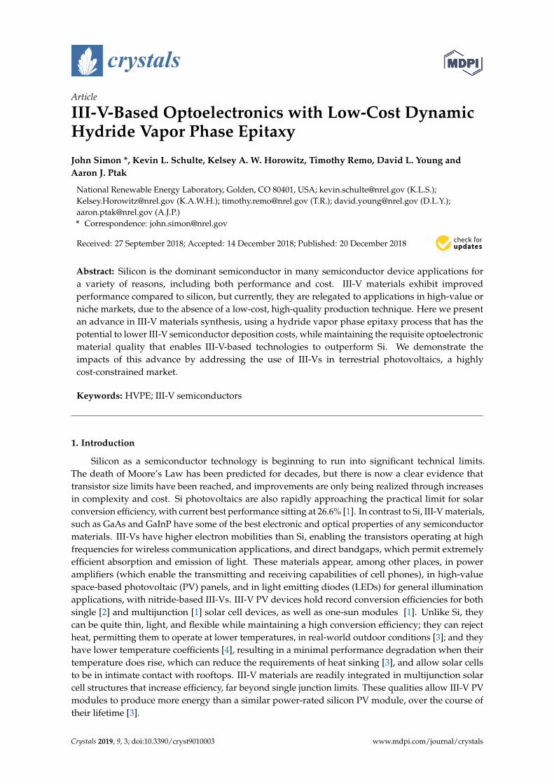
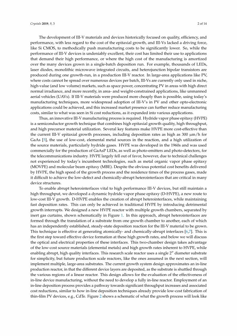
To enable abrupt heterointerfaces vital to high performance III-V devices, but still maintain ahigh throughput, we developed a dynamic hydride vapor phase epitaxy (D-HVPE), a new route tolow-cost III-V growth. D-HVPE enables the creation of abrupt heterointerfaces, while maintainingfast deposition rates. This can only be achieved in traditional HVPE by introducing detrimentalgrowth interrupts. We designed a new HVPE reactor with multiple growth chambers, separated byinert gas curtains, shown schematically in Figure 1. In this approach, abrupt heterointerfaces areformed through the translation of a substrate from one growth chamber to another, each of whichhas an independently established, steady-state deposition reaction for the III-V material to be grown.This technique is effective at generating atomically- and chemically-abrupt interfaces [6,7]. This isthe first step toward effective device formation at these high growth rates, and below we will discussthe optical and electrical properties of these interfaces. This two-chamber design takes advantageof the low-cost source materials (elemental metals) and high growth rates inherent to HVPE, whileenabling abrupt, high quality interfaces. This research scale reactor uses a single 2′′ diameter substratefor simplicity, but future production scale reactors, like the ones assumed in the next section, willimplement multiple, large-area substrates. The current growth system design approximates an in-lineproduction reactor, in that the different device layers are deposited, as the substrate is shuttled throughthe various regions of a linear reactor. This design allows for the evaluation of the effectiveness ofin-line device manufacturing, without the need to develop a fully in-line reactor. Employment of anin-line deposition process provides a pathway towards significant throughput increases and associatedcost reductions, similar to how in-line deposition techniques already provide low-cost fabrication ofthin-film PV devices, e.g., CdTe. Figure 2 shows a schematic of what the growth process will look like
Crystals 2019, 9, 3 3 of 14
in a multi-chamber HVPE reactor that is capable of growing a high-efficiency single-junction GaAssolar cell in minutes, instead of the hours that it takes with the current manufacturing technology.
Crystals 2018, 8, x 2 of 13
The development of III-V materials and devices historically focused on quality, efficiency, and performance, with less regard to the cost of the epitaxial growth, and III-Vs lacked a driving force, like Si CMOS, to methodically push manufacturing costs to be significantly lower. So, while the performance of III-V devices is undeniably excellent, their cost has limited their use to applications that demand their high performance, or where the high cost of the manufacturing is amortized over the many devices grown in a single-batch deposition run. For example, thousands of LEDs, laser diodes, monolithic microwave integrated circuits, and heterojunction bipolar transistors are produced during one growth-run, in a production III-V reactor. In large-area applications like PV, where costs cannot be spread over numerous devices per batch, III-Vs are currently only used in niche, high-value (and low volume) markets, such as space power, concentrating PV in areas with high direct normal irradiance, and more recently, in area- and weight-constrained applications, like unmanned aerial vehicles (UAVs). If III-V materials were produced more cheaply than is possible, using today’s manufacturing techniques, more widespread adoption of III-V’s in PV and other opto-electronic applications could be achieved, and this increased market presence can further reduce manufacturing costs, similar to what was seen in Si cost reductions, as it expanded into various applications.
Thus, an innovative III-V manufacturing process is required. Hydride vapor phase epitaxy (HVPE) is a semiconductor growth technique that combines high epitaxial growth quality, high throughput, and high precursor material utilization. Several key features make HVPE more cost-effective than the current III-V epitaxial growth processes, including deposition rates as high as 300 µm/h for GaAs [5], the use of low-cost, elemental metal sources in the reaction, and a high utilization of the source materials, particularly hydride gases. HVPE was developed in the 1960s and was used commercially for the production of GaAsP LEDs, as well as photo-emitters and photo-detectors, for the telecommunications industry. HVPE largely fell out of favor, however, due to technical challenges not experienced by today’s incumbent technologies, such as metal organic vapor phase epitaxy (MOVPE) and molecular beam epitaxy (MBE). Despite the obvious potential cost benefits delivered by HVPE, the high speed of the growth process and the residence times of the process gases, made it difficult to achieve the low-defect and chemically-abrupt heterointerfaces that are critical in many device structures.
Figure 1. Schematic of the two-chamber dynamic hydride vapor phase epitaxy (D-HVPE) reactor at NREL, showing the side-by-side steady-state reactions for GaAs and GaInP. The substrate is rapidly shuttled between the growth chambers to create high-quality, chemically-abrupt interfaces.
To enable abrupt heterointerfaces vital to high performance III-V devices, but still maintain a high throughput, we developed a dynamic hydride vapor phase epitaxy (D-HVPE), a new route to low-cost III-V growth. D-HVPE enables the creation of abrupt heterointerfaces, while maintaining fast deposition rates. This can only be achieved in traditional HVPE by introducing detrimental
Figure 1. Schematic of the two-chamber dynamic hydride vapor phase epitaxy (D-HVPE) reactor atNREL, showing the side-by-side steady-state reactions for GaAs and GaInP. The substrate is rapidlyshuttled between the growth chambers to create high-quality, chemically-abrupt interfaces.
Crystals 2018, 8, x 3 of 13
growth interrupts. We designed a new HVPE reactor with multiple growth chambers, separated by inert gas curtains, shown schematically in Figure 1. In this approach, abrupt heterointerfaces are formed through the translation of a substrate from one growth chamber to another, each of which has an independently established, steady-state deposition reaction for the III-V material to be grown. This technique is effective at generating atomically- and chemically-abrupt interfaces [6,7]. This is the first step toward effective device formation at these high growth rates, and below we will discuss the optical and electrical properties of these interfaces. This two-chamber design takes advantage of the low-cost source materials (elemental metals) and high growth rates inherent to HVPE, while enabling abrupt, high quality interfaces. This research scale reactor uses a single 2” diameter substrate for simplicity, but future production scale reactors, like the ones assumed in the next section, will implement multiple, large-area substrates. The current growth system design approximates an in-line production reactor, in that the different device layers are deposited, as the substrate is shuttled through the various regions of a linear reactor. This design allows for the evaluation of the effectiveness of in-line device manufacturing, without the need to develop a fully in-line reactor. Employment of an in-line deposition process provides a pathway towards significant throughput increases and associated cost reductions, similar to how in-line deposition techniques already provide low-cost fabrication of thin-film PV devices, e.g., CdTe. Figure 2 shows a schematic of what the growth process will look like in a multi-chamber HVPE reactor that is capable of growing a high-efficiency single-junction GaAs solar cell in minutes, instead of the hours that it takes with the current manufacturing technology.
Figure 2. Schematic of the in-line HVPE reactor used to grow low-cost single junction GaAs solar cells, together with a substrate reuse technology.
In the next sections, we will examine the economic viability of D-HVPE and then demonstrated that this technique can be used to produce devices with a comparable performance to MOVPE grown devices. We developed a cost model for the HVPE growth of III-V devices, using a linear, in-line deposition system, conceptually similar to that shown in Figure 2. The cost analysis showed that it is possible for III-Vs to be dramatically less expensive than they are today. We focused on the specific case of using D-HVPE for the production of III-V-based solar cells, which could enable competitiveness in various cost-sensitive terrestrial PV applications, with market sizes that increase as substrate costs (which are concurrently the subject of intense research) are reduced. In the final section, we described the current efforts to produce defect-free interfaces and high-efficiency single-junction GaAs solar cells, using our custom D-HVPE growth system as an example of devices possible, using this technique. We demonstrated solar conversion efficiencies >25.3% in the initial single-junction GaAs device grown at ~ 60 µm/h, similar to the efficiency of devices grown using the traditional growth technology. We also showed the initial results for the monolithic, HVPE-grown, two-junction GaInP/GaAs solar cell devices that incorporate three separate electrical junctions in a single device. The combination of low-cost growth, with the demonstration of high-efficiency
Figure 2. Schematic of the in-line HVPE reactor used to grow low-cost single junction GaAs solar cells,together with a substrate reuse technology.
In the next sections, we will examine the economic viability of D-HVPE and then demonstratedthat this technique can be used to produce devices with a comparable performance to MOVPE growndevices. We developed a cost model for the HVPE growth of III-V devices, using a linear, in-linedeposition system, conceptually similar to that shown in Figure 2. The cost analysis showed that it ispossible for III-Vs to be dramatically less expensive than they are today. We focused on the specificcase of using D-HVPE for the production of III-V-based solar cells, which could enable competitivenessin various cost-sensitive terrestrial PV applications, with market sizes that increase as substrate costs(which are concurrently the subject of intense research) are reduced. In the final section, we describedthe current efforts to produce defect-free interfaces and high-efficiency single-junction GaAs solar cells,using our custom D-HVPE growth system as an example of devices possible, using this technique.We demonstrated solar conversion efficiencies >25.3% in the initial single-junction GaAs device grownat ~60 µm/h, similar to the efficiency of devices grown using the traditional growth technology.We also showed the initial results for the monolithic, HVPE-grown, two-junction GaInP/GaAs solar
Crystals 2019, 9, 3 4 of 14
cell devices that incorporate three separate electrical junctions in a single device. The combinationof low-cost growth, with the demonstration of high-efficiency devices, illustrates the promise of theD-HVPE technique, not only for solar cells, but for all III-V device applications.
2. HVPE Deposition Costs
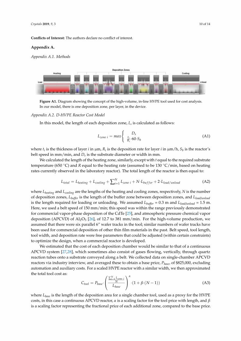
We performed an analysis of the potential impact of the HVPE process on III-V deposition costs,using NREL’s established bottom-up methodology [8–11]. For this analysis, we assumed that theNREL two-chamber HVPE reactor was scaled up to a high-volume, continuous reactor, with one zonefor heating the substrate and one deposition zone per layer, as illustrated schematically in MethodsFigure A1 in Appendix A. The deposition zones were isolated, using buffer sections incorporatinginert gas curtains. As no such high volume HVPE reactor exists today, we created a basic model of thesystem to estimate throughput and cost per tool; this model was reviewed by members of the industryand their feedback was incorporated for accuracy. Details of the model appear in Appendix A and inReference [12].
Cost of the HVPE-Grown III-V Photovoltaic Devices
We focused more specifically on the use of HVPE to produce low-cost, high-efficiency, III-V solarcells, and their potential competitiveness in different markets. If commercialized, D-HVPE couldimmediately provide value to PV markets that require high efficiency, high specific power, or flexibleform factors (including consumer electronics, UAVs, the military, space markets, and automotiveroofs [13]), by reducing the cost of epitaxy, while providing a performance similar to what is availabletoday. The overall benefit depends on the cell type, production volume, and processes used for otheraspects of the cell fabrication (e.g., metallization and choice of substrate), for a given manufacturer.
As discussed above, III-V solar cells at one-sun have not previously penetrated the mainstreamPV power markets, due to their prohibitively high cost. In this section, we assess the potential forD-HVPE and substrate reuse to enable III-V technology, to compete in some of these markets, bymodeling high volume costs for the III-V solar cells fabricated using these processes. We explore theirpotential balance-of-system (BOS) (e.g., racking materials and installation costs) and levelized thecost of energy (LCOE) (e.g., cost to produce a kWh of electricity) advantages over the incumbent Siflat-plate technology.
Our cell-cost models indicate that, at scale and with significant reductions in substrate cost, dualjunction InGaP/GaAs cells deposited via HVPE could potentially reach costs below $0.50/W, evenwith US manufacturing. This could allow these solar cells to be competitive in some broader PVmarkets that would benefit from the high-power density, low operating temperature and temperaturecoefficient, and the lightweight, flexible form factor, provided by III-V materials. Applications couldinclude, for example, PV tile roofs, PV on electric vehicles (EVs), and certain residential and commercialrooftop installations that are weight- or area-constrained. In fact, at <$0.50/W, III-V solar cells mayeven be competitive when dropped into the traditional PV module and system designs due to theability of efficiency to reduce BOS costs in certain markets. In the remainder of this section, we explorethe case of residential rooftop systems, which have higher BOS costs and areal constraints than thetypical ground-mount, utility-scale installations, and thus, stand to benefit more significantly from theincreased efficiency associated with III-V devices. We compared the total installed system cost andLCOE for the incumbent monocrystalline Si PERC [14] technology, to that of the HVPE-deposited III-Vcells with a substrate reuse. PERC cells were chosen for comparison because they are rapidly gainingtraction and are anticipated to become market-dominant over the next few years [15]. We used themodeled cell and module prices for both technologies that include the overhead costs and a sustainableproduct margin, rather than using current Si PERC cell prices, for the Si case, in order to obtain atechnology-based comparison. The details and assumptions of this model appear in the methodssection and Table A1 of Appendix A. The results are shown in Figure 3. While the III-V single junctioncell costs are higher than that for the PERC cells, the increased efficiency of the III-V single junction
Crystals 2019, 9, 3 5 of 14
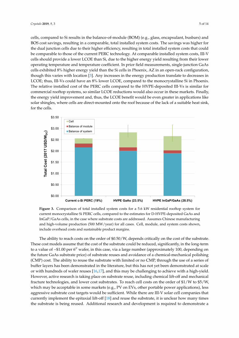
cells, compared to Si results in the balance-of-module (BOM) (e.g., glass, encapsulant, busbars) andBOS cost savings, resulting in a comparable, total installed system costs. The savings was higher forthe dual junction cells due to their higher efficiency, resulting in total installed system costs that couldbe comparable to those of the current PERC technology. At comparable installed system costs, III-Vcells should provide a lower LCOE than Si, due to the higher energy yield resulting from their loweroperating temperature and temperature coefficient. In prior field measurements, single-junction GaAscells exhibited 8% higher energy yield than the Si cells in Phoenix, AZ in an open-rack configuration,though this varies with location [3]. Any increases in the energy production translate to decreases inLCOE; thus, III-Vs could have an 8% lower LCOE, compared to the monocrystalline Si in Phoenix.The relative installed cost of the PERC cells compared to the HVPE-deposited III-Vs is similar forcommercial rooftop systems, so similar LCOE reductions would also occur in these markets. Finally,the energy yield improvement and, thus, the LCOE benefit would be even greater in applications likesolar shingles, where cells are direct-mounted onto the roof because of the lack of a suitable heat sink,for the cells.
Crystals 2018, 8, x 5 of 13
their higher efficiency, resulting in total installed system costs that could be comparable to those of the current PERC technology. At comparable installed system costs, III-V cells should provide a lower LCOE than Si, due to the higher energy yield resulting from their lower operating temperature and temperature coefficient. In prior field measurements, single-junction GaAs cells exhibited 8% higher energy yield than the Si cells in Phoenix, AZ in an open-rack configuration, though this varies with location [3]. Any increases in the energy production translate to decreases in LCOE; thus, III-Vs could have an 8% lower LCOE, compared to the monocrystalline Si in Phoenix. The relative installed cost of the PERC cells compared to the HVPE-deposited III-Vs is similar for commercial rooftop systems, so similar LCOE reductions would also occur in these markets. Finally, the energy yield improvement and, thus, the LCOE benefit would be even greater in applications like solar shingles, where cells are direct-mounted onto the roof because of the lack of a suitable heat sink, for the cells.
Figure 3. Comparison of total installed system costs for a 5.6kW residential rooftop system for current monocrystalline Si PERC cells, compared to the estimates for D-HVPE-deposited GaAs and InGaP/GaAs cells, in the case where substrate costs are addressed. Assumes Chinese manufacturing and high-volume production (500 MW/year) for all cases. Cell, module, and system costs shown, include overhead costs and sustainable product margins.
The ability to reach costs on the order of $ 0.50/W, depends critically on the cost of the substrate. These cost models assume that the cost of the substrate could be reduced, significantly, in the long-term to a value of ~ $1.00 per 6” wafer, in this case, via a large number (approximately 100, depending on the future GaAs substrate price) of substrate reuses and avoidance of a chemical-mechanical polishing (CMP) cost. The ability to reuse the substrate with limited or no CMP, through the use of a series of buffer layers has been demonstrated in the literature, but this has not yet been demonstrated at scale or with hundreds of wafer reuses [16,17], and this may be challenging to achieve with a high-yield. However, active research is taking place on substrate reuse, including chemical lift-off and mechanical fracture technologies, and lower cost substrates. To reach cell costs on the order of $ 1/W to $ 5/W, which may be acceptable in some markets (e.g., PV on EVs, other portable power applications), less aggressive substrate cost targets would be sufficient. While there are III-V solar cell companies that currently implement the epitaxial lift-off [18] and reuse the substrate, it is unclear how many times the substrate is being reused. Additional research and development is required to demonstrate a hundred reuses, at scale with a high-yield and significantly reduced polishing and reclaim costs. The lift-off process itself must also be scaled-up; current production volumes for III-V cells are low. Alternatively, cost reductions could be achieved via the use of a low-cost substrate (e.g., a virtual substrate or template, direct-growth on a low-cost substrate), as long as similar efficiencies
$0.00
$0.50
$1.00
$1.50
$2.00
$2.50
$3.00
$3.50
Current c-Si PERC (19%) HVPE GaAs (23.5%) HVPE InGaP/GaAs (28.5%)
Tota
l Cos
t (20
17 U
SD/W
DC)
Cell
Balance of module
Balance of system
Figure 3. Comparison of total installed system costs for a 5.6 kW residential rooftop system forcurrent monocrystalline Si PERC cells, compared to the estimates for D-HVPE-deposited GaAs andInGaP/GaAs cells, in the case where substrate costs are addressed. Assumes Chinese manufacturingand high-volume production (500 MW/year) for all cases. Cell, module, and system costs shown,include overhead costs and sustainable product margins.
The ability to reach costs on the order of $0.50/W, depends critically on the cost of the substrate.These cost models assume that the cost of the substrate could be reduced, significantly, in the long-termto a value of ~$1.00 per 6′′ wafer, in this case, via a large number (approximately 100, depending onthe future GaAs substrate price) of substrate reuses and avoidance of a chemical-mechanical polishing(CMP) cost. The ability to reuse the substrate with limited or no CMP, through the use of a series ofbuffer layers has been demonstrated in the literature, but this has not yet been demonstrated at scaleor with hundreds of wafer reuses [16,17], and this may be challenging to achieve with a high-yield.However, active research is taking place on substrate reuse, including chemical lift-off and mechanicalfracture technologies, and lower cost substrates. To reach cell costs on the order of $1/W to $5/W,which may be acceptable in some markets (e.g., PV on EVs, other portable power applications), lessaggressive substrate cost targets would be sufficient. While there are III-V solar cell companies thatcurrently implement the epitaxial lift-off [18] and reuse the substrate, it is unclear how many timesthe substrate is being reused. Additional research and development is required to demonstrate a
Crystals 2019, 9, 3 6 of 14
hundred reuses, at scale with a high-yield and significantly reduced polishing and reclaim costs.The lift-off process itself must also be scaled-up; current production volumes for III-V cells are low.Alternatively, cost reductions could be achieved via the use of a low-cost substrate (e.g., a virtualsubstrate or template, direct-growth on a low-cost substrate), as long as similar efficiencies can beobtained, or a combination of the two (lower cost substrate that is reused a lower number of times).
The cost model presented here does assume the immediate implementation of the technologypresented in this paper. In addition to the time to commercialize and scale-up the D-HVPE process, thesubstrate advances will require time and investments in research and development. However, becausethe results in Figure 3 are based on the 2017 module and system cost structures, and include modeled2017 Si PERC cell costs, these comparisons essentially assume these III-V cell costs were achievedovernight. While this serves to illustrate the benefits of a higher III-V cell efficiency at the module andsystem level and provides a useful benchmark for understanding whether or not III-V cells might beapplicable to general power markets, some additional discussion of the future is warranted. FurtherBOM and BOS cost reductions are anticipated in the future [19]. These reductions would benefit bothSi and III-Vs, but the marginal value of higher efficiencies, and thus, the advantage of the III-V cellsover Si, would be somewhat reduced. Additionally, the efficiencies of Si systems are also anticipatedto rise, although they are beginning to hit the practical limits [20], and Si module costs are expected todecrease, but will similarly asymptote, eventually, as the technology is already quite mature. We werenot able to make quantitative comparisons of the installed system costs in these future scenarios dueto the lack of PV cost-projections and general uncertainty around the future system cost structures.Finally, Figure 3 includes only the costs associated with single and dual junction III-V cells; HVPEcould potentially allow for the addition of even more junctions at a low cost when scaled, increasingefficiencies further and enabling additional BOM and BOS cost savings that are out of reach for Si.
3. Development of D-HVPE for High Efficiency Devices
HVPE was successfully employed in the past to produce commercial devices, such as LEDs anddetectors, but the production of HVPE-grown III-V devices paled in comparison to the MOVPE growndevices [21,22], primarily due to the difficulty of making abrupt, highly-passivated heterointerfaces,as noted earlier. This is important because unpassivated interfaces have dangling atomic bonds orimpurities that would otherwise act as non-radiative recombination sites and decrease the deviceperformance. It is important that the potential low costs of the HVPE growth, detailed in the previoussection, be viewed in the context of the achievable performance. The key test for D-HVPE is toeffectively passivate III-V layers to decrease the carrier recombination at interface states, while stillmaintaining the high throughput that helps to make HVPE a low-cost technology.
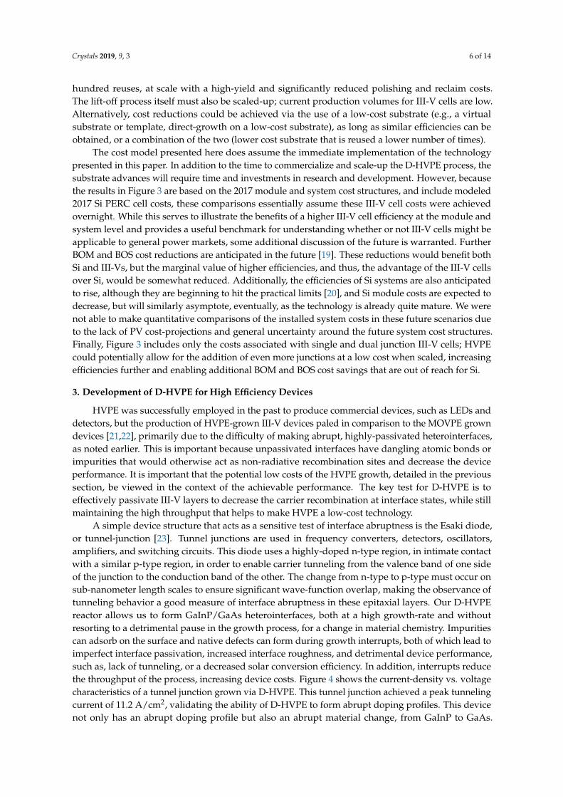
A simple device structure that acts as a sensitive test of interface abruptness is the Esaki diode,or tunnel-junction [23]. Tunnel junctions are used in frequency converters, detectors, oscillators,amplifiers, and switching circuits. This diode uses a highly-doped n-type region, in intimate contactwith a similar p-type region, in order to enable carrier tunneling from the valence band of one sideof the junction to the conduction band of the other. The change from n-type to p-type must occur onsub-nanometer length scales to ensure significant wave-function overlap, making the observance oftunneling behavior a good measure of interface abruptness in these epitaxial layers. Our D-HVPEreactor allows us to form GaInP/GaAs heterointerfaces, both at a high growth-rate and withoutresorting to a detrimental pause in the growth process, for a change in material chemistry. Impuritiescan adsorb on the surface and native defects can form during growth interrupts, both of which lead toimperfect interface passivation, increased interface roughness, and detrimental device performance,such as, lack of tunneling, or a decreased solar conversion efficiency. In addition, interrupts reducethe throughput of the process, increasing device costs. Figure 4 shows the current-density vs. voltagecharacteristics of a tunnel junction grown via D-HVPE. This tunnel junction achieved a peak tunnelingcurrent of 11.2 A/cm2, validating the ability of D-HVPE to form abrupt doping profiles. This devicenot only has an abrupt doping profile but also an abrupt material change, from GaInP to GaAs.
Crystals 2019, 9, 3 7 of 14
The extremely low resistance across this tunnel diode (Figure 4 inset), allows us to use it in multijunctionsolar-cell structures to connect two subcells in series such that the voltages of the individual subcellsadd together to create a structure with a high solar conversion efficiency [24]. This indicates thatD-HVPE is capable of creating heterojunctions that are thin, chemically abrupt, and free of detrimentaldefects that would lower the achievable performance necessary for a high-peak-current tunneling.
Crystals 2018, 8, x 7 of 13
abrupt, and free of detrimental defects that would lower the achievable performance necessary for a high-peak-current tunneling.
Figure 4. Current-density-voltage characteristics for a tunnel junction grown using D-HVPE. Inset shows an amplified look around 0 V showing the low resistance of the tunnel junction.
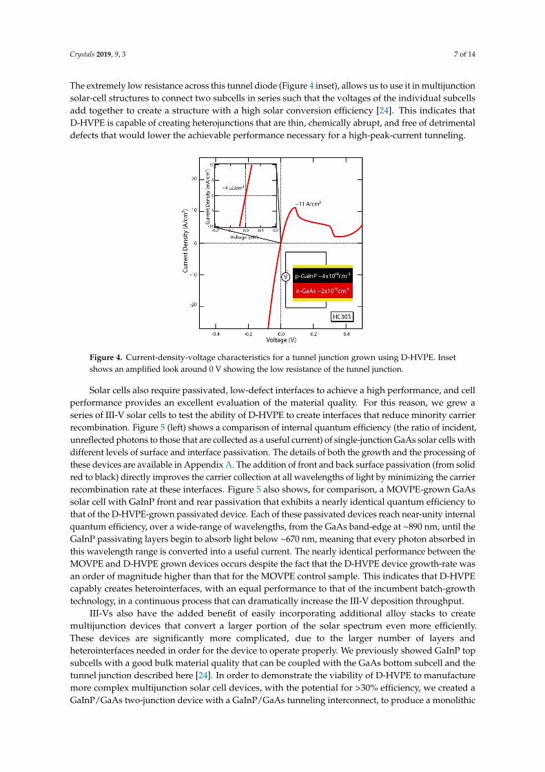
Solar cells also require passivated, low-defect interfaces to achieve a high performance, and cell performance provides an excellent evaluation of the material quality. For this reason, we grew a series of III-V solar cells to test the ability of D-HVPE to create interfaces that reduce minority carrier recombination. Figure 5 (left) shows a comparison of internal quantum efficiency (the ratio of incident, unreflected photons to those that are collected as a useful current) of single-junction GaAs solar cells with different levels of surface and interface passivation. The details of both the growth and the processing of these devices are available in Appendix A. The addition of front and back surface passivation (from solid red to black) directly improves the carrier collection at all wavelengths of light by minimizing the carrier recombination rate at these interfaces. Figure 5 also shows, for comparison, a MOVPE-grown GaAs solar cell with GaInP front and rear passivation that exhibits a nearly identical quantum efficiency to that of the D-HVPE-grown passivated device. Each of these passivated devices reach near-unity internal quantum efficiency, over a wide-range of wavelengths, from the GaAs band-edge at ~ 890 nm, until the GaInP passivating layers begin to absorb light below ~ 670 nm, meaning that every photon absorbed in this wavelength range is converted into a useful current. The nearly identical performance between the MOVPE and D-HVPE grown devices occurs despite the fact that the D-HVPE device growth-rate was an order of magnitude higher than that for the MOVPE control sample. This indicates that D-HVPE capably creates heterointerfaces, with an equal performance to that of the incumbent batch-growth technology, in a continuous process that can dramatically increase the III-V deposition throughput.
Figure 5. (Left) Internal quantum efficiency measurements of an unpassivated (red), and a fully
Figure 4. Current-density-voltage characteristics for a tunnel junction grown using D-HVPE. Insetshows an amplified look around 0 V showing the low resistance of the tunnel junction.
Solar cells also require passivated, low-defect interfaces to achieve a high performance, and cellperformance provides an excellent evaluation of the material quality. For this reason, we grew aseries of III-V solar cells to test the ability of D-HVPE to create interfaces that reduce minority carrierrecombination. Figure 5 (left) shows a comparison of internal quantum efficiency (the ratio of incident,unreflected photons to those that are collected as a useful current) of single-junction GaAs solar cells withdifferent levels of surface and interface passivation. The details of both the growth and the processing ofthese devices are available in Appendix A. The addition of front and back surface passivation (from solidred to black) directly improves the carrier collection at all wavelengths of light by minimizing the carrierrecombination rate at these interfaces. Figure 5 also shows, for comparison, a MOVPE-grown GaAssolar cell with GaInP front and rear passivation that exhibits a nearly identical quantum efficiency tothat of the D-HVPE-grown passivated device. Each of these passivated devices reach near-unity internalquantum efficiency, over a wide-range of wavelengths, from the GaAs band-edge at ~890 nm, until theGaInP passivating layers begin to absorb light below ~670 nm, meaning that every photon absorbed inthis wavelength range is converted into a useful current. The nearly identical performance between theMOVPE and D-HVPE grown devices occurs despite the fact that the D-HVPE device growth-rate wasan order of magnitude higher than that for the MOVPE control sample. This indicates that D-HVPEcapably creates heterointerfaces, with an equal performance to that of the incumbent batch-growthtechnology, in a continuous process that can dramatically increase the III-V deposition throughput.
III-Vs also have the added benefit of easily incorporating additional alloy stacks to createmultijunction devices that convert a larger portion of the solar spectrum even more efficiently.These devices are significantly more complicated, due to the larger number of layers andheterointerfaces needed in order for the device to operate properly. We previously showed GaInP topsubcells with a good bulk material quality that can be coupled with the GaAs bottom subcell and thetunnel junction described here [24]. In order to demonstrate the viability of D-HVPE to manufacturemore complex multijunction solar cell devices, with the potential for >30% efficiency, we created aGaInP/GaAs two-junction device with a GaInP/GaAs tunneling interconnect, to produce a monolithic
Crystals 2019, 9, 3 8 of 14
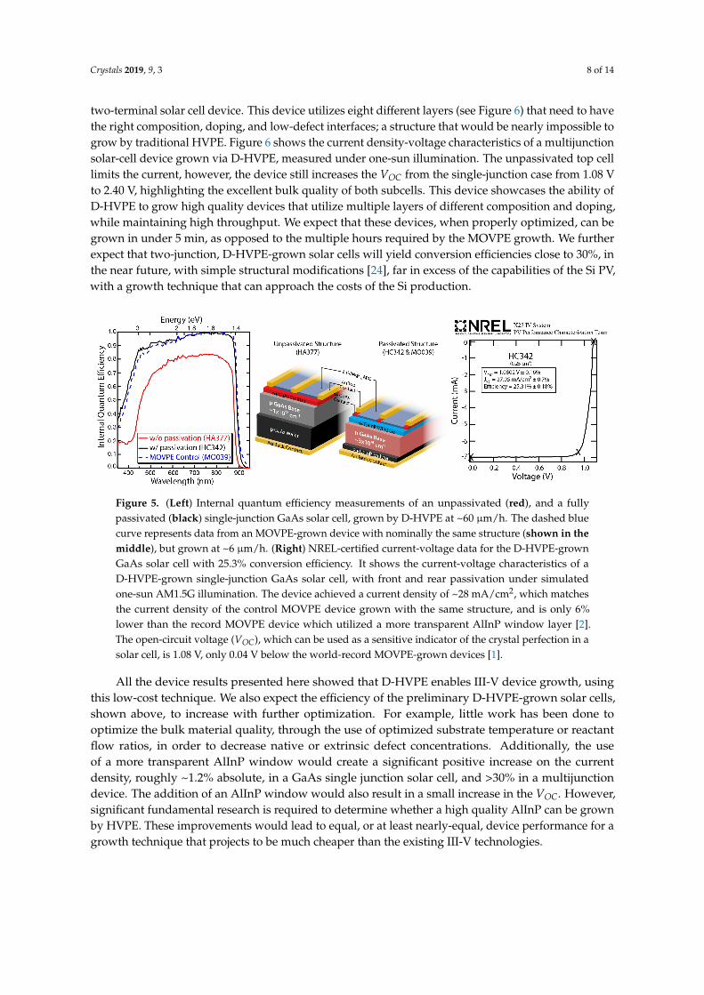
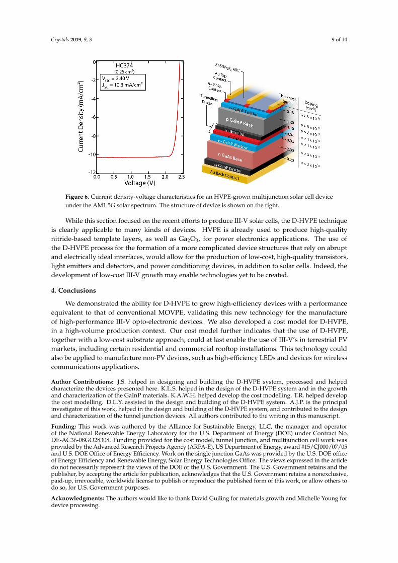
two-terminal solar cell device. This device utilizes eight different layers (see Figure 6) that need to havethe right composition, doping, and low-defect interfaces; a structure that would be nearly impossible togrow by traditional HVPE. Figure 6 shows the current density-voltage characteristics of a multijunctionsolar-cell device grown via D-HVPE, measured under one-sun illumination. The unpassivated top celllimits the current, however, the device still increases the VOC from the single-junction case from 1.08 Vto 2.40 V, highlighting the excellent bulk quality of both subcells. This device showcases the ability ofD-HVPE to grow high quality devices that utilize multiple layers of different composition and doping,while maintaining high throughput. We expect that these devices, when properly optimized, can begrown in under 5 min, as opposed to the multiple hours required by the MOVPE growth. We furtherexpect that two-junction, D-HVPE-grown solar cells will yield conversion efficiencies close to 30%, inthe near future, with simple structural modifications [24], far in excess of the capabilities of the Si PV,with a growth technique that can approach the costs of the Si production.
Crystals 2018, 8, x 7 of 13
abrupt, and free of detrimental defects that would lower the achievable performance necessary for a high-peak-current tunneling.
Figure 4. Current-density-voltage characteristics for a tunnel junction grown using D-HVPE. Inset shows an amplified look around 0 V showing the low resistance of the tunnel junction.
Solar cells also require passivated, low-defect interfaces to achieve a high performance, and cell performance provides an excellent evaluation of the material quality. For this reason, we grew a series of III-V solar cells to test the ability of D-HVPE to create interfaces that reduce minority carrier recombination. Figure 5 (left) shows a comparison of internal quantum efficiency (the ratio of incident, unreflected photons to those that are collected as a useful current) of single-junction GaAs solar cells with different levels of surface and interface passivation. The details of both the growth and the processing of these devices are available in Appendix A. The addition of front and back surface passivation (from solid red to black) directly improves the carrier collection at all wavelengths of light by minimizing the carrier recombination rate at these interfaces. Figure 5 also shows, for comparison, a MOVPE-grown GaAs solar cell with GaInP front and rear passivation that exhibits a nearly identical quantum efficiency to that of the D-HVPE-grown passivated device. Each of these passivated devices reach near-unity internal quantum efficiency, over a wide-range of wavelengths, from the GaAs band-edge at ~ 890 nm, until the GaInP passivating layers begin to absorb light below ~ 670 nm, meaning that every photon absorbed in this wavelength range is converted into a useful current. The nearly identical performance between the MOVPE and D-HVPE grown devices occurs despite the fact that the D-HVPE device growth-rate was an order of magnitude higher than that for the MOVPE control sample. This indicates that D-HVPE capably creates heterointerfaces, with an equal performance to that of the incumbent batch-growth technology, in a continuous process that can dramatically increase the III-V deposition throughput.
Figure 5. (Left) Internal quantum efficiency measurements of an unpassivated (red), and a fully
Figure 5. (Left) Internal quantum efficiency measurements of an unpassivated (red), and a fullypassivated (black) single-junction GaAs solar cell, grown by D-HVPE at ~60 µm/h. The dashed bluecurve represents data from an MOVPE-grown device with nominally the same structure (shown in themiddle), but grown at ~6 µm/h. (Right) NREL-certified current-voltage data for the D-HVPE-grownGaAs solar cell with 25.3% conversion efficiency. It shows the current-voltage characteristics of aD-HVPE-grown single-junction GaAs solar cell, with front and rear passivation under simulatedone-sun AM1.5G illumination. The device achieved a current density of ~28 mA/cm2, which matchesthe current density of the control MOVPE device grown with the same structure, and is only 6%lower than the record MOVPE device which utilized a more transparent AlInP window layer [2].The open-circuit voltage (VOC), which can be used as a sensitive indicator of the crystal perfection in asolar cell, is 1.08 V, only 0.04 V below the world-record MOVPE-grown devices [1].
All the device results presented here showed that D-HVPE enables III-V device growth, usingthis low-cost technique. We also expect the efficiency of the preliminary D-HVPE-grown solar cells,shown above, to increase with further optimization. For example, little work has been done tooptimize the bulk material quality, through the use of optimized substrate temperature or reactantflow ratios, in order to decrease native or extrinsic defect concentrations. Additionally, the useof a more transparent AlInP window would create a significant positive increase on the currentdensity, roughly ~1.2% absolute, in a GaAs single junction solar cell, and >30% in a multijunctiondevice. The addition of an AlInP window would also result in a small increase in the VOC. However,significant fundamental research is required to determine whether a high quality AlInP can be grownby HVPE. These improvements would lead to equal, or at least nearly-equal, device performance for agrowth technique that projects to be much cheaper than the existing III-V technologies.
Crystals 2019, 9, 3 9 of 14
Crystals 2018, 8, x 8 of 13
passivated (black) single-junction GaAs solar cell, grown by D-HVPE at ~ 60 μm/h. The dashed blue curve represents data from an MOVPE-grown device with nominally the same structure (shown in the middle), but grown at ~ 6 µm/h. (Right) NREL-certified current-voltage data for the D-HVPE-grown GaAs solar cell with 25.3% conversion efficiency. It shows the current-voltage characteristics of a D-HVPE-grown single-junction GaAs solar cell, with front and rear passivation under simulated one-sun AM1.5G illumination. The device achieved a current density of ~28 mA/cm2, which matches the current density of the control MOVPE device grown with the same structure, and is only 6% lower than the record MOVPE device which utilized a more transparent AlInP window layer [2]. The open-circuit voltage (VOC), which can be used as a sensitive indicator of the crystal perfection in a solar cell, is 1.08 V, only 0.04 V below the world-record MOVPE-grown devices [1].
III-Vs also have the added benefit of easily incorporating additional alloy stacks to create multijunction devices that convert a larger portion of the solar spectrum even more efficiently. These devices are significantly more complicated, due to the larger number of layers and heterointerfaces needed in order for the device to operate properly. We previously showed GaInP top subcells with a good bulk material quality that can be coupled with the GaAs bottom subcell and the tunnel junction described here [24]. In order to demonstrate the viability of D-HVPE to manufacture more complex multijunction solar cell devices, with the potential for >30% efficiency, we created a GaInP/GaAs two-junction device with a GaInP/GaAs tunneling interconnect, to produce a monolithic two-terminal solar cell device. This device utilizes eight different layers (see Figure 6) that need to have the right composition, doping, and low-defect interfaces; a structure that would be nearly impossible to grow by traditional HVPE. Figure 6 shows the current density-voltage characteristics of a multijunction solar-cell device grown via D-HVPE, measured under one-sun illumination. The unpassivated top cell limits the current, however, the device still increases the VOC from the single-junction case from 1.08 V to 2.40 V, highlighting the excellent bulk quality of both subcells. This device showcases the ability of D-HVPE to grow high quality devices that utilize multiple layers of different composition and doping, while maintaining high throughput. We expect that these devices, when properly optimized, can be grown in under 5 min, as opposed to the multiple hours required by the MOVPE growth. We further expect that two-junction, D-HVPE-grown solar cells will yield conversion efficiencies close to 30%, in the near future, with simple structural modifications,24 far in excess of the capabilities of the Si PV, with a growth technique that can approach the costs of the Si production.
Figure 6. Current density-voltage characteristics for an HVPE-grown multijunction solar cell device under the AM1.5G solar spectrum. The structure of device is shown on the right.
All the device results presented here showed that D-HVPE enables III-V device growth, using this low-cost technique. We also expect the efficiency of the preliminary D-HVPE-grown solar cells, shown above, to increase with further optimization. For example, little work has been done to optimize the bulk material quality, through the use of optimized substrate temperature or reactant
Figure 6. Current density-voltage characteristics for an HVPE-grown multijunction solar cell deviceunder the AM1.5G solar spectrum. The structure of device is shown on the right.
While this section focused on the recent efforts to produce III-V solar cells, the D-HVPE techniqueis clearly applicable to many kinds of devices. HVPE is already used to produce high-qualitynitride-based template layers, as well as Ga2O3, for power electronics applications. The use ofthe D-HVPE process for the formation of a more complicated device structures that rely on abruptand electrically ideal interfaces, would allow for the production of low-cost, high-quality transistors,light emitters and detectors, and power conditioning devices, in addition to solar cells. Indeed, thedevelopment of low-cost III-V growth may enable technologies yet to be created.
4. Conclusions
We demonstrated the ability for D-HVPE to grow high-efficiency devices with a performanceequivalent to that of conventional MOVPE, validating this new technology for the manufactureof high-performance III-V opto-electronic devices. We also developed a cost model for D-HVPE,in a high-volume production context. Our cost model further indicates that the use of D-HVPE,together with a low-cost substrate approach, could at last enable the use of III-V’s in terrestrial PVmarkets, including certain residential and commercial rooftop installations. This technology couldalso be applied to manufacture non-PV devices, such as high-efficiency LEDs and devices for wirelesscommunications applications.
Author Contributions: J.S. helped in designing and building the D-HVPE system, processed and helpedcharacterize the devices presented here. K.L.S. helped in the design of the D-HVPE system and in the growthand characterization of the GaInP materials. K.A.W.H. helped develop the cost modelling. T.R. helped developthe cost modelling. D.L.Y. assisted in the design and building of the D-HVPE system. A.J.P. is the principalinvestigator of this work, helped in the design and building of the D-HVPE system, and contributed to the designand characterization of the tunnel junction devices. All authors contributed to the writing in this manuscript.
Funding: This work was authored by the Alliance for Sustainable Energy, LLC, the manager and operatorof the National Renewable Energy Laboratory for the U.S. Department of Energy (DOE) under Contract No.DE-AC36-08GO28308. Funding provided for the cost model, tunnel junction, and multijunction cell work wasprovided by the Advanced Research Projects Agency (ARPA-E), US Department of Energy, award #15/CJ000/07/05and U.S. DOE Office of Energy Efficiency. Work on the single junction GaAs was provided by the U.S. DOE officeof Energy Efficiency and Renewable Energy, Solar Energy Technologies Office. The views expressed in the articledo not necessarily represent the views of the DOE or the U.S. Government. The U.S. Government retains and thepublisher, by accepting the article for publication, acknowledges that the U.S. Government retains a nonexclusive,paid-up, irrevocable, worldwide license to publish or reproduce the published form of this work, or allow others todo so, for U.S. Government purposes.
Acknowledgments: The authors would like to thank David Guiling for materials growth and Michelle Young fordevice processing.
Crystals 2019, 9, 3 10 of 14
Conflicts of Interest: The authors declare no conflict of interest.
Appendix A.
Appendix A.1. MethodsCrystals 2018, 8, x 10 of 13
Methods Figure 1. Diagram showing the concept of the high-volume, in-line HVPE tool used for cost analysis. In our model, there is one deposition zone, per layer, in the device.
A2. D-HVPE Reactor Cost Model
In this model, the length of each deposition zone, L, is calculated as follows:
𝐿 = 𝑚𝑎𝑥 𝐷𝑡𝑅 ∙ 60 ∙ 𝑆 (1)
where ti is the thickness of layer i in µm, Ri is the deposition rate for layer i in µm/h, Sb is the reactor’s belt speed in mm/min, and Ds is the substrate diameter or width in mm.
We calculated the length of the heating zone, similarly, except with t equal to the required substrate temperature (650 °C) and R equal to the heating rate (assumed to be 130 °C/min, based on heating rates currently observed in the laboratory reactor). The total length of the reactor is then equal to: 𝐿 = 𝐿 + 𝐿 + 𝐿 + 𝑁 ∙ 𝐿 + 2 ∙ 𝐿 / (2)
where Lheating and Lcooling are the lengths of the heating and cooling zones, respectively, N is the number of deposition zones, Lbuffer is the length of the buffer zone between deposition zones, and Lload/unload is the length required for loading or unloading. We assumed Lbuffer = 0.3 m and Lload/unload = 1.5 m. Here, we used a belt speed of 150 mm/min; this speed was within the range previously demonstrated for commercial vapor-phase deposition of the CdTe [25], and atmospheric pressure chemical vapor deposition (APCVD) of Al2O3 [26], of 12.7 to 381 mm/min. For the high-volume production, we assumed that there were six parallel 6” wafer tracks in the tool; similar numbers of wafer tracks have been used for commercial deposition of other thin film materials in the past. Belt speed, tool length, tool width, and deposition rate were free parameters that could be adjusted (within certain constraints) to optimize the design, when a commercial reactor is developed.
We estimated that the cost of each deposition chamber would be similar to that of a continuous APCVD system [27,28], which sometimes also consist of gases flowing, vertically, through quartz reaction tubes onto a substrate conveyed along a belt. We collected data on single-chamber APCVD reactors via industry interview, and averaged these to obtain a base price, Pbase, of $ 825,000, excluding automation and auxiliary costs. For a scaled HVPE reactor with a similar width, we then approximated the total tool cost as:
𝐶 = 𝑃 ∙ ∑ 𝐿 𝑁𝐿 ∙ (1 + 𝛽 ∙ (𝑁 − 1)) (3)
where Lbase is the length of the deposition area for a single chamber tool, used as a proxy for the HVPE costs, in this case a continuous APCVD reactor, α is a scaling factor for the tool price with length, and β is a scaling factor representing the fractional price of each additional zone, compared to the base price. Both α and β contain significant uncertainty at this point; however, based on interviews with several major suppliers of high-volume deposition equipment, we approximated the tool costs using α = 0.75 and β = 0.6. Sensitivity analysis showed that the cost advantages of the HVPE deposition were robust to a range of α and β values.
Key assumptions made in the deposition cost analysis are summarized in Table 1. Material price values were based on quotes received from material suppliers, interviews with members of industries
Figure A1. Diagram showing the concept of the high-volume, in-line HVPE tool used for cost analysis.In our model, there is one deposition zone, per layer, in the device.
Appendix A.2. D-HVPE Reactor Cost Model
In this model, the length of each deposition zone, L, is calculated as follows:
Lzone i = max
{Ds
tiRi·60·Sb
(A1)
where ti is the thickness of layer i in µm, Ri is the deposition rate for layer i in µm/h, Sb is the reactor’sbelt speed in mm/min, and Ds is the substrate diameter or width in mm.
We calculated the length of the heating zone, similarly, except with t equal to the required substratetemperature (650 ◦C) and R equal to the heating rate (assumed to be 130 ◦C/min, based on heatingrates currently observed in the laboratory reactor). The total length of the reactor is then equal to:
Ltotal = Lheating + Lcooling + ∑Ni=1 Lzone i + N·Lbu f f er + 2·Lload/unload (A2)
where Lheating and Lcooling are the lengths of the heating and cooling zones, respectively, N is the numberof deposition zones, Lbuffer is the length of the buffer zone between deposition zones, and Lload/unloadis the length required for loading or unloading. We assumed Lbuffer = 0.3 m and Lload/unload = 1.5 m.Here, we used a belt speed of 150 mm/min; this speed was within the range previously demonstratedfor commercial vapor-phase deposition of the CdTe [25], and atmospheric pressure chemical vapordeposition (APCVD) of Al2O3 [26], of 12.7 to 381 mm/min. For the high-volume production, weassumed that there were six parallel 6” wafer tracks in the tool; similar numbers of wafer tracks havebeen used for commercial deposition of other thin film materials in the past. Belt speed, tool length,tool width, and deposition rate were free parameters that could be adjusted (within certain constraints)to optimize the design, when a commercial reactor is developed.
We estimated that the cost of each deposition chamber would be similar to that of a continuousAPCVD system [27,28], which sometimes also consist of gases flowing, vertically, through quartzreaction tubes onto a substrate conveyed along a belt. We collected data on single-chamber APCVDreactors via industry interview, and averaged these to obtain a base price, Pbase, of $825,000, excludingautomation and auxiliary costs. For a scaled HVPE reactor with a similar width, we then approximatedthe total tool cost as:
Ctool = Pbase·
∑Ni=1 Lzone i
NLbase
α
·(1 + β·(N − 1)) (A3)
where Lbase is the length of the deposition area for a single chamber tool, used as a proxy for the HVPEcosts, in this case a continuous APCVD reactor, α is a scaling factor for the tool price with length, and β
is a scaling factor representing the fractional price of each additional zone, compared to the base price.
Crystals 2019, 9, 3 11 of 14
Both α and β contain significant uncertainty at this point; however, based on interviews with severalmajor suppliers of high-volume deposition equipment, we approximated the tool costs using α = 0.75and β = 0.6. Sensitivity analysis showed that the cost advantages of the HVPE deposition were robustto a range of α and β values.
Key assumptions made in the deposition cost analysis are summarized in Table A1. Materialprice values were based on quotes received from material suppliers, interviews with members ofindustries that purchased the materials, and (where relevant) aggregation of data from online metalpricing sources and the US Geological Survey. All material pricing was based on the assumption ofa high-volume production and large orders. For HVPE deposition, we assumed additional costs forautomation and auxiliary equipment and installation equal to 22% and 20% of the total tool price,respectively. The material utilization rates for the MOVPE were based on prior work [10], and havebeen validated again by some industry members, as recently as 2018. Material utilization rates for theHVPE are currently uncertain. A Ga and In utilization of 70% was calculated from our research scaleHVPE reactor. For all analysis, we assumed U.S. manufacturing and a 100% plant capacity utilization.
Appendix A.3. D-HVPE III-V Solar-Cell Cost Model
We modeled the cell costs using the NREL cost model for single and dual junction III-V solar cells,under one sun illumination, first published in Reference [10]. The cost model was refined and updatedin 2018, in order to reflect the current pricing for equipment and materials, as well as changes in processor capability. Figure 5 shows the device stacks modelled here. Low-cost metallization compatiblewith processing and epitaxial lift-off (ELO) of the III-Vs is still under development. Our cost modelassumes the cell contacts are fabricated, using a low-cost plating, without the use of gold. We alsoassumed a high-volume ELO of the GaAs substrate and ≥100 substrate reuses, without requiringchemical-mechanical polishing (CMP). The ability to reuse the substrate with limited or no CMP,through the use of a series of buffer layers has been demonstrated in the literature, but this has not yetbeen demonstrated at scale or with hundreds of wafer reuses [16,17], and this may be challenging toachieve with a high yield. However, active research is taking place on the substrate reuse, includingchemical lift-off and mechanical fracture technologies, and a low-cost process with a high number ofreuses may be feasible in the long-term.
Table A1. Key Input Assumptions for the HVPE Deposition Cost Model.
Input Value
Ga price (6N) $0.21/gIn price (6N) $0.82/g
High purity AsH3 price $0.48/gHigh purity PH3 price $0.55/gGa material utilization 70%In material utilization 70%
AsH3 material utilization 30%PH3 material utilization 30%
H2 curtain flow rate 10,000 sccmHCl carrier gas flow rate 14.5 sccm
Tool length 7.3 m (1 J cell), 9.6 m (2 J cell)Tool price (including automation and auxiliary equipment) $4.7 million (1 J), $11.6 million (2 J cell)
Equipment maintenance cost 4% of total equipment cost/year
We further assumed that III-V cells can be dropped into the standard modules employed forthe c-Si cells. We used the NREL’s module cost model to calculate the module cost and minimumsustainable price (MSP) (see References [8–11] for a description of MSP). The module MSP was inputinto the NREL’s system cost models for residential, commercial, and utility scale systems [29] toevaluate the total system cost.
Crystals 2019, 9, 3 12 of 14
Appendix A.4. D-HVPE III-V Material Growth Methods
All materials and devices shown in this work were grown in our dual chamber, Dynamic-HVPE(D-HVPE) reactor [30], using pure Ga and In metal, HCl, AsH3, PH3, and H2 carrier gas. Dilute H2Sewas the n-type dopant, while dimethylzinc was the p-type dopant. Heterointerfaces were formedby rapid mechanical transfer of the substrate between the two growth chambers, with each chamberstabilized at a new growth condition (either a change in material, doping, or both) for at least oneminute before transfer. Substrates were (100) n+ GaAs doped with Si and offcut 4◦ towards the (111)Bplane. The growth rates of the GaAs absorber layers were 60 µm/h, while the tunnel junction GaAsand GaInP layers were grown at 6 µm/h. The GaInP absorber in the tandem device was grown at54 µm/h. An n+ GaAs buffer was grown to bury contamination at the initial growth interface, beforedevice growth.
Solar cell devices were processed using the method detailed in Reference [31]. Unpassivateddevices were processed on wafer, while passivated devices were grown inverted and removed fromthe wafer. First, a broad area Au contact was electroplated onto the back-contact layer. The Au surfacewas bonded to a Si handle, using an epoxy and the substrate was selectively etched away, usinga NH4OH/H2O2/H2O 1:2:2 solution, exposing a GaInP etch stop layer. This layer was removed,selectively, with hydrochloric acid. A grid pattern was defined by the standard lithography techniques,and Ni/Au front contact grids were electroplated for the front grid contacts of all devices. Finally, 5 mm× 5 mm area devices were defined by lithography and isolated using selective wet chemical etching.
We measured solar cell external quantum efficiency (EQE) on a custom instrument, in whichchopped, monochromatic light was split and then sent to the device of interest and a calibrated,broadband reference diode. We measured the output current of the device and reference on a lock-inamplifier, and used it to calculate the EQE, which is the ratio of electron current out to incident photons.Specular reflectance from the device surface was measured with a separate, calibrated reference diode.
We compared the measured EQEs to those of the calibrated GaInP and GaAs reference cells, tocalculate the spectral correction factors for the AM1.5G spectrum. We set the height of a Xe-lampsolar simulator to obtain an illumination of 1000 W/cm2, determined by measuring the current fromthe reference GaAs cell held under the lamp and adjusting by the spectral correction factor for thesubcell of interest. We set dual junction top cell illumination by placing the GaInP reference cell,under the lamp at the GaAs one-sun height, and added current using a 470 nm LED to obtain one-sunequivalent illumination. The tandem cell one-sun current density-voltage curves were measured underthe adjusted spectrum.
References
1. Green, M.A.; Hishikawa, Y.; Warta, W.; Dunlop, E.D.; Levi, D.H.; Hohl-Ebinger, J.; Ho-Baillie, A.W.H. SolarCell Efficiency Tables (Version 50). Prog. Photovolt. Res. Appl. 2017, 25, 668–676. [CrossRef]
2. Kayes, B.M.; Nie, H.; Twist, R.; Spruytte, S.G.; Reinhardt, F.; Kizilyalli, I.C.; Higashi, G.S. 27.6% Conversionefficiency, a new record for single-junction solar cells under 1 sun illumination. In Proceedings of the 37thIEEE Photovoltaic Specialists Conference, Seattle, WA, USA, 19–24 June 2011.
3. Silverman, T.J.; Deceglie, M.G.; Marion, B.; Cowley, S.; Kayes, B.; Kurtz, S. Outdoor Performance of aThin-Film Gallium-Arsenide Photovoltaic Module. In Proceedings of the IEEE 39th Photovoltaic SpecialistsConference (PVSC), Tampa, FL, USA, 16–21 June 2013.
4. Osterwald, C.R.; Glatfelter, T.; Burdick, J. Comparison of the Temperature Coefficients of the Basic I-VParameters for Various Types of Solar Cells. In Proceedings of the Nineteenth IEEE Photovoltaic SpecialistsConference, New Orleans, LA, USA, 4–8 May 1987.
5. Deschler, M.; Grüter, K.; Schlegel, A.; Beccard, R.; Jürgensen, H.; Balk, P. Very Rapid Growth of High QualityGaAs, InP and Related III-V Compounds. J. Phys. Colloq. 1988, 49, 689–692. [CrossRef]
6. Jain, N.; Simon, J.; Schulte, K.L.; Friedman, D.J.; Diercks, D.R.; Packard, C.E.; Young, D.L.; Ptak, A.J.Tunable Bandgap GaInAsP Solar Cells With 18.7% Photoconversion Efficiency Synthesized by Low-Cost andHigh-Growth Rate Hydride Vapor Phase Epitaxy. IEEE J. Photovolt. 2018, 99, 1–7. [CrossRef]
Crystals 2019, 9, 3 13 of 14
7. Schulte, K.L.; Simon, J.; Mangum, J.; Packard, C.E.; Gorman, B.P.; Jain, N.; Ptak, A.J. Development of GaInPSolar Cells Grown by Hydride Vapor Phase Epitaxy. IEEE J. Photovolt. 2017, 7, 1153–1158. [CrossRef]
8. Goodrich, A.; Hacke, P.; Wang, Q.; Sopori, B.; Margolis, R.; James, T.L.; Woodhouse, M. A wafer-basedmonocrystalline silicon photovoltaics road map: Utilizing k nown technology improvement opportunitiesfor further reductions in manufacturing costs. Sol. Energy Mater. Sol. Cells 2013, 114, 110–135. [CrossRef]
9. Horowitz, K.A.; Woodhouse, M.; Lee, H.; Smestad, G.P. A Bottom-Up Cost Analysis of a High ConcentrationPV Module. In AIP Conference Proceedings; AIP Publishing: College Park, MD, USA, 2016.
10. Woodhouse, M.; Goodrich, A. A Manufacturing Cost Analysis Relevant to Single- and Dual-JunctionPhotovoltaic Cells Fabricated with III-Vs and III-Vs Grown on Czochralski Silicon. Available online: http://www.nrel.gov/docs/fy14osti/60126.pdf (accessed on 14 December 2018).
11. Woodhouse, M.; Jones-Albertus, R.; Feldman, D.; Fu, R.; Horowitz, K.; Chung, D.; Jordan, D.; Kurtz, S. Onthe Path to SunShot: The Role of Advancements in Solar Photovoltaic Efficiency, Reliability, and Costs.Available online: http://www.nrel.gov/docs/fy16osti/65872.pdf (accessed on 14 December 2018).
12. Horowitz, K.A.W.; Remo, T.; Smith, B.; Ptak, A. Techno-Economic Analysis and Cost Reduction Roadmap for III-VSolar Cells; National Renewable Energy Lab. (NREL): Golden, CO, USA, 2018.
13. Audi Cooperates with Alta Devices on Automobiles with Solar Roofs. Available online: https://www.altadevices.com/audi-cooperates-alta-devices-automobiles-solar-roofs/ (accessed on 14 December 2018).
14. Green, M.A. The Passivated Emitter and Rear Cell (PERC): From conception to mass production. Sol. EnergyMater. Sol. Cells 2015, 143, 190–197. [CrossRef]
15. VDMA. International Technology Roadmap for Photovoltaic. 2017. Available online: http://www.etip-pv.eu/fileadmin/Documents/ETIP_PV_Conference_2017_Presentations/Session_II._1._Axel_Metz.pdf(accessed on 14 December 2018).
16. Ward, J.S.; Remo, T.; Horowitz, K.; Woodhouse, M.; Sopori, B.; VanSant, K.; Basore, P. Techno-economicanalysis of three different substrate removal and reuse strategies for III-V solar cells. Prog. Photovolt. Res. Appl.2016, 24, 1284–1292. [CrossRef]
17. Lee, K.; Zimmerman, J.D.; Xiao, X.; Sun, K.; Forrest, S.R. Forrest. Reuse of GaAs substrates for epitaxiallift-off by employing protection layers. J. Appl. Phys. 2012, 111, 033527. [CrossRef]
18. Yablonovitch, E.; Gmitter, T.; Harbison, J.P.; Bhat, R. Extreme selectivity in the lift-off of epitaxial GaAs films.Appl. Phys. Lett. 1987, 51, 2222. [CrossRef]
19. Cole, W.; Mai, T.; Richards, J.; Das, P. 2017 Standard Scenarios Report: A U.S. Electricity Sector Outlook.Available online: https://www.nrel.gov/docs/fy18osti/68548.pdf (accessed on 14 December 2018).
20. Shockley, W.; Queisser, H.J. Detailed Balance Limit of Efficiency of p-n Junction Solar Cells. J. Appl. Phys.1961, 32, 510–519. [CrossRef]
21. Gale, R.P.; McClelland, R.W.; King, B.D.; Fan, J.C.C. Thin-film solar cells with over 21% conversion efficiency.Sol. Cell 1989, 27, 99–106. [CrossRef]
22. Usui, A.; Matsumoto, T.; Inai, M.; Mito, I.; Kobayashi, K.; Watanabe, H. Room Temperature cw Operation ofVisible InGaAsP Double Heterostructure Laser at 671 nm Grown by Hydride VPE. Jpn. J. Appl. Phys. 1985,24, L163. [CrossRef]
23. Esaki, L. New Phenomenon in Narrow Germanium p−n Junctions. Phys. Rev. 1958, 109, 603–604. [CrossRef]24. Schulte, K.L.; Simon, J.; Ptak, A. Multijunction GaInP/GaAs Solar Cells Grown by Hydride Vapor Phase
Epitaxy. Prog. Photovolt. 2018, 26, 887–893. [CrossRef]25. Kaydanov, V.I.; Ohno, T.R. Process Development and Basic Studies of Electrochemically Deposited
CdTe-Based Solar Cells. Available online: http://www.nrel.gov/docs/fy01osti/29956.pdf (accessed on 14December 2018).
26. Black, L.E. New Perspectives on Surface Passivation: Understanding the Si-Al2O3 Interface; Springer: Basel,Switzerland, 2016.
27. Chemical Vapor Deposition. Available online: http://users.wfu.edu/ucerkb/Nan242/L10-CVD_b.pdf(accessed on 14 December 2018).
28. Williams, J.D. Microfabrication and Semiconductor Processes. Available online: http://www.slideshare.net/maheeniqbal1420/part-6-thin-film-depositoin (accessed on 14 December 2018).
29. Fu, R.; Feldman, D.; Margolis, R.; Woodhouse, M.; Ardani, K.U.S. Solar Photovoltaic System Cost Benchmark:Q1 2017. Available online: https://www.nrel.gov/docs/fy17osti/68925.pdf (accessed on 14 December 2018).

Crystals 2019, 9, 3 14 of 14
30. Young, D.L.; Ptak, A.J.; Kuech, T.F.; Schulte, K.; Simon, J.D. High Throughput Semiconductor Deposition System(No. 9,824,890); National Renewable Energy Lab. (NREL): Golden, CO, USA, 2017.
31. Duda, A.; Ward, J.S.; Young, M. Inverted Metamorphic Multijunction (IMM) Cell Processing Instructions (No.NREL/TP-5200-54049); National Renewable Energy Lab. (NREL): Golden, CO, USA, 2012.
© 2018 by the authors. Licensee MDPI, Basel, Switzerland. This article is an open accessarticle distributed under the terms and conditions of the Creative Commons Attribution(CC BY) license (http://creativecommons.org/licenses/by/4.0/).