cs 61c: great ideas in computer architecture functional units
TRANSCRIPT

Instructor: Justin Hsia
7/25/2013 Summer 2013 ‐‐ Lecture #19 1
CS 61C: Great Ideas in Computer Architecture
Functional Units,Finite State Machines

Review of Last Lecture
• Synchronous Digital Systems– Pulse of a Clock controls flow of information– All signals are seen as either 0 or 1
• Hardware systems are constructed from StatelessCombinational Logic and Stateful “Memory” Logic (registers)
• Combinational Logic: equivalent circuit diagrams, truth tables, and Boolean expressions– Boolean Algebra allows minimization of gates
• State registers implemented from Flip‐flops7/25/2013 Summer 2013 ‐‐ Lecture #19 2

Dealing with Waveform Diagrams
• Easiest to start with CLK on top– Solve signal by signal, from inputs to outputs– Can only draw the waveform for a signal if all of its input waveforms are drawn
• When does a signal update?– A state element updates based on CLK triggers– A combinational element updates ANY time ANY of its inputs changes
7/25/2013 Summer 2013 ‐‐ Lecture #19 3

4
Example: T = 10 ns. tsetup = thold = 0. tclk‐to‐q = 1 ns. tprop = 1 ns for all gates. Each “tick” below is 1 ns.Solve for the waveform of the output Y.

system
datapath control
stateregisters
combinationallogicmultiplexer comparatorcode
registers
register logic
switchingnetworks
Hardware Design Hierarchy
7/25/2013 Summer 2013 ‐‐ Lecture #19 5
Today

Agenda
• State Elements Continued• Administrivia• Logisim Introduction• Finite State Machines• Multiplexers• ALU Design
– Adder/Subtracter
7/25/2013 Summer 2013 ‐‐ Lecture #19 6

Model for Synchronous Systems
7/25/2013 Summer 2013 ‐‐ Lecture #19 7
• Collection of Combinational Logic blocks separated by registers– Feedback is optional depending on application
• Clock (CLK): square wave that synchronizes the system– Clock signal connects only to clock input of registers
• Register: several bits of state that samples input on rising edge of CLK

Accumulator Revisited...Again
7/25/2013 Summer 2013 ‐‐ Lecture #19 8
• reset signal shown
• In practice X might not arrive to the adder at the same time as Si‐1
• Si temporarily is wrong, but register always captures correct value
• In good circuits, instability never happens around rising edge of clk

Register Timing Terms (Review)
• Setup Time: how long the input must be stable before the CLK trigger for proper input read
• Hold Time: how long the input must be stable after the CLK trigger for proper input read
• “CLK‐to‐Q” Delay: how long it takes the output to change, measured from the CLK trigger
7/25/2013 Summer 2013 ‐‐ Lecture #19 9
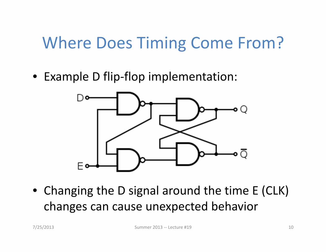
Where Does Timing Come From?
• Example D flip‐flop implementation:
• Changing the D signal around the time E (CLK) changes can cause unexpected behavior
7/25/2013 Summer 2013 ‐‐ Lecture #19 10

Maximum Clock Frequency
• What is the max frequency of this circuit?– Limited by how much time needed to get correct Next State to Register
7/25/2013 Summer 2013 ‐‐ Lecture #19 11
Max Delay =
Max Freq = 1/Max Delay
Setup Time + CLK‐to‐Q Delay+ CL Delay

+Reg
Reg
The Critical Path
• The critical path is the longest delay between any two registers in a circuit
• The clock period must be longer than this critical path, or the signal will not propagate properly to that next register
7/25/2013 Summer 2013 ‐‐ Lecture #19 12
12
3
4
Critical Path =CL Delay 1+ CL Delay 2+ CL Delay 3+ Adder Delay

Pipelining and Clock Frequency (1/2)• Clock period limited by propagation delay of adder and shifter– Add an extra register to reduce the critical path!
7/25/2013 Summer 2013 ‐‐ Lecture #19 13
Timing:

7/25/2013 Summer 2013 ‐‐ Lecture #19 14
Pipelining and Clock Frequency (2/2)• Extra register allows higher clock freq (more outputs per sec)• However, takes two (shorter) clock cycles to produce first
output (higher latency for initial output)
+ setup time + CLK‐to‐Q delay
+ CLK‐to‐Q delay
+ Adder delay
+ Shifter delay
+ setup time + CLK‐to‐Q delay

Pipelining Basics
• By adding more registers, break path into shorter “stages”– Aim is to reduce critical path– Signals take an additional clock cycle to propagate through each stage
• New critical path must be calculated– Affected by placement of new pipelining registers– Faster clock rate higher throughput (outputs)– More stages higher startup latency
• Pipelining tends to improve performance– More on this (application to CPUs) next week
7/25/2013 Summer 2013 ‐‐ Lecture #19 15

16
Question: Want to run on 1 GHz processor.tadd = 100 ps. tmult = 200 ps. tsetup = thold = 50 ps. What is the maximum tclk‐to‐q we can use?
550 ps(A)
750 ps(B)
500 ps(C)(D)

Agenda
• State Elements Continued• Administrivia• Logisim Introduction• Finite State Machines• Multiplexers• ALU Design
– Adder/Subtracter
7/25/2013 Summer 2013 ‐‐ Lecture #19 17

• Midterm re‐grade requests due today– We will re‐grade the entire test
• Project 2 Part 2 will be posted today• HW5 posted today, due Thu Aug. 1
7/25/2013 Summer 2013 ‐‐ Lecture #19 18
Administrivia

Agenda
• State Elements Continued• Administrivia• Logisim Introduction• Finite State Machines• Multiplexers• ALU Design
– Adder/Subtracter
7/25/2013 Summer 2013 ‐‐ Lecture #19 19
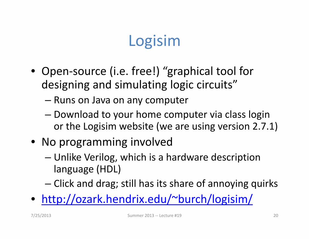
Logisim
• Open‐source (i.e. free!) “graphical tool for designing and simulating logic circuits”– Runs on Java on any computer– Download to your home computer via class login or the Logisim website (we are using version 2.7.1)
• No programming involved– Unlike Verilog, which is a hardware description language (HDL)
– Click and drag; still has its share of annoying quirks• http://ozark.hendrix.edu/~burch/logisim/7/25/2013 Summer 2013 ‐‐ Lecture #19 20

Gates in Logisim
• Click gate type, click to place– Can set options before placing or select gate later to change
7/25/2013 Summer 2013 ‐‐ Lecture #19 21
Options
Types of Gates
bus width n
# inputs
labeling not necessary,but can help

Registers in Logisim
• Flip‐flops and Registers in “Memory” folder• 8‐bit accumulator:
7/25/2013 Summer 2013 ‐‐ Lecture #19 22

Wires in Logisim
• Click and drag on existing port or wire• Color schemes:
– Gray: unconnected– Dark Green: low signal (0)– Light Green: high signal (1)– Red: error– Blue: undetermined signal– Orange: incompatible widths
• Tunnels: all tunnels with same label are connected
7/25/2013 Summer 2013 ‐‐ Lecture #19 23
“Splitter” used to adjust bus widths

• Connecting wires together– Crossing wires vs. connected wires
• Losing track of which input is which– Mis‐wiring a block (e.g. CLK to Enable)– Grabbing wrong wires off of splitter
• Errors:
7/25/2013 Summer 2013 ‐‐ Lecture #19 24
Common Mistakes in Logisim

Agenda
• State Elements Continued• Administrivia• Logisim Introduction• Finite State Machines• Multiplexers• ALU Design
– Adder/Subtracter
7/25/2013 Summer 2013 ‐‐ Lecture #19 25

Finite State Machines (FSMs)
• You may have seen FSMs in other classes• Function can be represented with a state transition diagram
• With combinational logic and registers, any FSM can be implemented in hardware!
7/25/2013 Summer 2013 ‐‐ Lecture #19 26
. . .

• An FSM (in this class) is defined by:– A set of states S (circles)– An initial state s0 (only arrow not between states)– A transition function that maps from the current input and current state to the output and the next state (arrows between states)
• State transitions are controlled by the clock: – On each clock cycle the machine checks the inputs and generates a new state (could be same) and new output
7/25/2013 Summer 2013 ‐‐ Lecture #19 27
FSM Overview

7/25/2013 Summer 2013 ‐‐ Lecture #19 28
• FSM to detect 3 consecutive 1’s in the Input
Example: 3 Ones FSM
States: S0, S1, S2Initial State: S0Transitions of form:
input/output

Hardware Implementation of FSM
• Register holds a representation of the FSM’s state– Must assign a unique bit pattern for each state– Output is present/current state (PS/CS)– Input is next state (NS)
• Combinational Logic implements transition function (state transitions + output)
7/25/2013 Summer 2013 ‐‐ Lecture #19 29
+ =

FSM: Combinational Logic
• Read off transitions into Truth Table!– Inputs: Current State (CS) and Input (In)– Outputs: Next State (NS) and Output (Out)
• Implement logic for EACH output (2 for NS, 1 for Out)7/25/2013 Summer 2013 ‐‐ Lecture #19 30
CS In NS Out00 0 00 000 1 01 001 0 00 001 1 10 010 0 00 010 1 00 1

Unspecified Output Values (1/2)
• Our FSM has only 3 states– 2 entries in truth table are undefined/unspecified
• Use symbol ‘X’ to mean it canbe either a 0 or 1– Make choice to simplify finalexpression
7/25/2013 Summer 2013 ‐‐ Lecture #19 31
CS In NS Out00 0 00 000 1 01 001 0 00 001 1 10 010 0 00 010 1 00 111 0 XX X11 1 XX X

Unspecified Output Values (2/2)
• Let’s find expression for NS1– Recall: 2‐bit output is just a2‐bit bus, which is just 2 wires
• Boolean algebra:– NS1 = CS1’CS0In + CS1CS0In’
+ CS1CS0In– NS1 = CS0In
• Karnaugh Map:– NS1 = CS0In
7/25/2013 Summer 2013 ‐‐ Lecture #19 32
CS In NS Out00 0 00 000 1 01 001 0 00 001 1 10 010 0 00 010 1 00 111 0 XX X11 1 XX X
Differs by 2
Is neighbor
00 01 11 10
0 0 0 X 0
1 0 1 X 0
CSIn

3 Ones FSM in Hardware
• 2‐bit Register needed for state• CL: NS1 = CS0In, NS0 = CS1’CS0’In, Out = CS1In
7/25/2013 Summer 2013 ‐‐ Lecture #19 33

Agenda
• State Elements Continued• Administrivia• Logisim Introduction• Finite State Machines• Multiplexers• ALU Design
– Adder/Subtracter
7/25/2013 Summer 2013 ‐‐ Lecture #19 34

Data Multiplexor
• Multiplexor (“MUX”) is a selector– Place one of multiple inputs onto output (N‐to‐1)
• Shown below is an n‐bit 2‐to‐1 MUX– Input S selects between two inputs of n bits each
7/25/2013 Summer 2013 ‐‐ Lecture #19 35
This input is passed to output if selector bits match shown value

Implementing a 1‐bit 2‐to‐1 MUX
• Schematic:
• Truth Table:
• Boolean Algebra:
• Circuit Diagram:
7/25/2013 Summer 2013 ‐‐ Lecture #19 36
s a b c0 0 0 00 0 1 00 1 0 10 1 1 11 0 0 01 0 1 11 1 0 01 1 1 1

1‐bit 4‐to‐1 MUX (1/2)
• Schematic:
• Truth Table: How many rows?• Boolean Expression:
e = s1’s0’a + s1’s0b + s1s0’c + s1s0d7/25/2013 Summer 2013 ‐‐ Lecture #19 37
26

1‐bit 4‐to‐1 MUX (2/2)
• Can we leverage what we’ve previously built?– Alternative hierarchical approach:
7/25/2013 Summer 2013 ‐‐ Lecture #19 38

Subcircuits Example• Logisim equivalent of procedure or method
– Every project is a hierarchy of subcircuits
7/25/2013 Summer 2013 ‐‐ Lecture #19 39
Incomplete wiring shown here

Get To Know Your Instructor
7/25/2013 Summer 2013 ‐‐ Lecture #19 40

Agenda
• State Elements Continued• Administrivia• Logisim Introduction• Finite State Machines• Multiplexers• ALU Design
– Adder/Subtracter
7/25/2013 Summer 2013 ‐‐ Lecture #19 41

• Most processors contain a special logic block called the “Arithmetic and Logic Unit” (ALU)– We’ll show you an easy one that does ADD, SUB, bitwise AND, and bitwise OR
• Schematic:
7/25/2013 Summer 2013 ‐‐ Lecture #19 42
Arithmetic and Logic Unit (ALU)
when S=00, R = A + Bwhen S=01, R = A – Bwhen S=10, R = A AND Bwhen S=11, R = A OR B

Simple ALU Schematic
7/25/2013 Summer 2013 ‐‐ Lecture #19 43
Notice that 3 values are ALWAYS calculated in parallel, but only 1 makes it to the Result

Adder/Subtractor: 1‐bit LSB Adder
7/25/2013 Summer 2013 ‐‐ Lecture #19 44
Carry‐out bit

Adder/Subtractor: 1‐bit Adder
7/25/2013 Summer 2013 ‐‐ Lecture #19 45
Here defining XOR of many inputs to be 1 when an odd number of inputs are 1
Possible carry‐in c1

Adder/Subtractor: 1‐bit Adder
7/25/2013 Summer 2013 ‐‐ Lecture #19 46
• Circuit Diagrams:

N x 1‐bit Adders N‐bit Adder
7/25/2013 Summer 2013 ‐‐ Lecture #19 47
+ + +b0
• Connect CarryOuti‐1 to CarryIni to chain adders:

Two’s Complement Adder/Subtractor
7/25/2013 Summer 2013 ‐‐ Lecture #19 48
+ + +
• Subtraction accomplished by adding negated number:
x ^ 1 = x’(flips the bits)
This signal is onlyhigh when youperform subtraction
Add 1
Where did this come from?
Detecting Overflow
7/25/2013 Summer 2013 ‐‐ Lecture #19 49
• Unsigned overflow – On addition, if carry‐out from MSB is 1– On subtraction, if carry‐out from MSB is 0
• This case is a lot harder to see than you might think
• Signed overflow1) Overflow from adding “large” positive numbers2) Overflow from adding “large” negative numbers
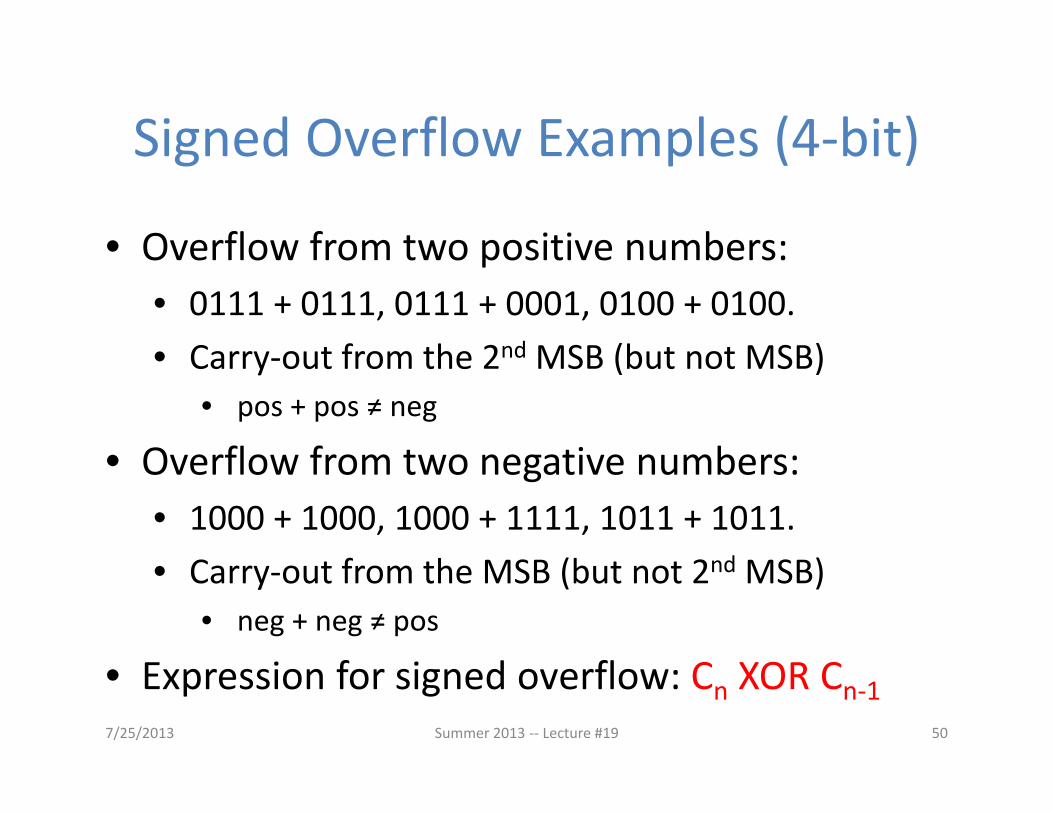
Signed Overflow Examples (4‐bit)
7/25/2013 Summer 2013 ‐‐ Lecture #19 50
• Overflow from two positive numbers:• 0111 + 0111, 0111 + 0001, 0100 + 0100.• Carry‐out from the 2nd MSB (but not MSB)
• pos + pos ≠ neg
• Overflow from two negative numbers:• 1000 + 1000, 1000 + 1111, 1011 + 1011.• Carry‐out from the MSB (but not 2nd MSB)
• neg + neg ≠ pos
• Expression for signed overflow: Cn XOR Cn‐1

• Critical path constrains clock rate– Timing constants: setup, hold, and clk‐to‐q times– Can adjust with extra registers (pipelining)
• Finite State Machines extremely useful– Can implement systems with Register + CL
• Use MUXes to select among input– S input bits selects one of 2S inputs– Each input is a bus n‐bits wide
• Build n‐bit adder out of chained 1‐bit adders– Can also do subtraction with additional SUB signal
7/25/2013 Summer 2013 ‐‐ Lecture #19 51
Summary

You are responsible for the material contained on the following slides, though we may not have enough time to get to them in lecture.They have been prepared in a way that should be easily readable and the material will be touched upon in the following lecture.
7/25/2013 Summer 2013 ‐‐ Lecture #19 52

Direct‐Mapped Cache Internals• Four words/block, cache size = 1 Ki words
7/25/2013 Summer 2013 ‐‐ Lecture #19 53
8Index
Data (words)Index TagValid012...
253254255
31 30 . . . 13 12 11 . . . 4 3 2 1 0Byte offset
20
20Tag
Hit Data
32
Block offset
and

4‐Way Set Associative Cache• 28 = 256 sets each with four slots for blocks
7/25/2013 Summer 2013 ‐‐ Lecture #19 54
31 30 . . . 13 12 11 . . . 2 1 0 Byte offset
DataTagV012...
253254255
DataTagV012...
253254255
DataTagV012...
253254255
Index DataTagV012...
253254255
8Index
22Tag
Hit Data
32
4x1 select