cs152 computer architecture and engineering lecture 8 ...pattrsn/152f97/... · computer...
TRANSCRIPT

cs 152 datapath.1 ©UCB, DAP’ 97
CS152Computer Architecture and Engineering
Lecture 8: Designing a Single Cycle Datapath
September 24, 1997
Dave Patterson (http.cs.berkeley.edu/~patterson)
lecture slides: http://www-inst.eecs.berkeley.edu/~cs152/

cs 152 datapath.2 ©UCB, DAP’ 97
Outline of Today’s Lecture
° Recap (5 minutes)
° Design a processor: step-by-step
° Requirements of the Instruction Set
° Questions and Administrative Matters (5 minutes)
° Components and Clocking
° Assembling an Adequate Datapath
° Break (5 minutes)
° Controling the datapath

cs 152 datapath.3 ©UCB, DAP’ 97
Review: Floating Point
° Define a number system representation that behaves very much like real numbers
• large dynamic range (-1038 to + 1038)• fine precision (10-38)
° Use “scientific notation”• normal form for the mantissa (±1.xxxxxxxx)• exponent specifies position of the binary point)
° Arithmetic algorithms just as in high school• Addition:
- shift number with smaller exponent right till have same scale
- add mantissas- renormalize
• Subtraction? Multiplication? Division?
°

cs 152 datapath.4 ©UCB, DAP’ 97
More Review° IEEE 754: rounding as if computed to full prec. and rounded
• requires carry, guard, and sticky bit
° IEEE 754: denorms, infinities, and NANs
° Divide can use same hardware as multiply: Hi & Lo registers in MIPS
° Bits have no inherent meaning: operations determine whether they are really ASCII characters, integers, floating point numbers
° Pentium: Difference between bugs that board designers must know about and bugs that potentially affect all users
• Why not make public complete description of bugs in later category?
• $200,000 cost in June to repair design
• $500,000,000 loss in December in profits to replace bad parts
• How much to repair Intel’s reputation?
° What is technologists responsibility in disclosing bugs?

cs 152 datapath.5 ©UCB, DAP’ 97
The Big Picture: Where are We Now?
° The Five Classic Components of a Computer
° Today’s Topic: Design a Single Cycle Processor
Control
Datapath
Memory
ProcessorInput
Output
inst. set design (L1-2) technology (L3)
machinedesign Arithmetic (L5-7)

cs 152 datapath.6 ©UCB, DAP’ 97
The Big Picture: The Performance Perspective° Performance of a machine is determined by:
• Instruction count
• Clock cycle time
• Clock cycles per instruction
° Processor design (datapath and control) will determine:
• Clock cycle time
• Clock cycles per instruction
° Today:
• Single cycle processor:
- Advantage: One clock cycle per instruction
- Disadvantage: long cycle time
CPI
Inst. Count Cycle Time
cs 152 datapath.7 ©UCB, DAP’ 97
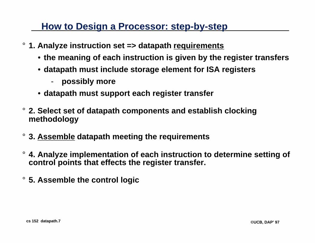
How to Design a Processor: step-by-step
° 1. Analyze instruction set => datapath requirements
• the meaning of each instruction is given by the register transfers
• datapath must include storage element for ISA registers
- possibly more
• datapath must support each register transfer
° 2. Select set of datapath components and establish clocking methodology
° 3. Assemble datapath meeting the requirements
° 4. Analyze implementation of each instruction to determine setting of control points that effects the register transfer.
° 5. Assemble the control logic
cs 152 datapath.8 ©UCB, DAP’ 97
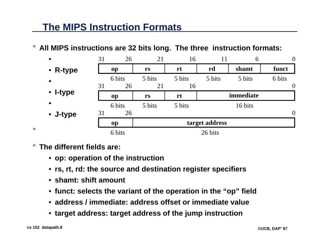
The MIPS Instruction Formats
° All MIPS instructions are 32 bits long. The three instruction formats:
•
• R-type
•
• I-type
•
• J-type
°
° The different fields are:
• op: operation of the instruction
• rs, rt, rd: the source and destination register specifiers
• shamt: shift amount
• funct: selects the variant of the operation in the “op” field
• address / immediate: address offset or immediate value
• target address: target address of the jump instruction
op target address
02631
6 bits 26 bits
op rs rt rd shamt funct
061116212631
6 bits 6 bits5 bits5 bits5 bits5 bits
op rs rt immediate016212631
6 bits 16 bits5 bits5 bits

cs 152 datapath.9 ©UCB, DAP’ 97
Step 1a: The MIPS-lite Subset for today
° ADD and SUB
• addU rd, rs, rt
• subU rd, rs, rt
° OR Immediate:
• ori rt, rs, imm16
° LOAD and STORE Word
• lw rt, rs, imm16
• sw rt, rs, imm16
° BRANCH:
• beq rs, rt, imm16
op rs rt rd shamt funct
061116212631
6 bits 6 bits5 bits5 bits5 bits5 bits
op rs rt immediate
016212631
6 bits 16 bits5 bits5 bits
op rs rt immediate
016212631
6 bits 16 bits5 bits5 bits
op rs rt immediate
016212631
6 bits 16 bits5 bits5 bits

cs 152 datapath.10 ©UCB, DAP’ 97
Logical Register Transfers
° RTL gives the meaning of the instructions
° All start by fetching the instructionop | rs | rt | rd | shamt | funct = MEM[ PC ]
op | rs | rt | Imm16 = MEM[ PC ]
inst Register Transfers
ADDU R[rd] <– R[rs] + R[rt]; PC <– PC + 4
SUBU R[rd] <– R[rs] – R[rt]; PC <– PC + 4
ORi R[rt] <– R[rs] + zero_ext(Imm16); PC <– PC + 4
LOAD R[rt] <– MEM[ R[rs] + sign_ext(Imm16)]; PC <– PC + 4
STORE MEM[ R[rs] + sign_ext(Imm16) ] <– R[rs];PC <– PC + 4
BEQ if ( R[rs] == R[rt] ) then PC <– PC + sign_ext(Imm16)] || 00
else PC <– PC + 4

cs 152 datapath.11 ©UCB, DAP’ 97
Step 1: Requirements of the Instruction Set
° Memory
• instruction & data
° Registers (32 x 32)
• read RS
• read RT
• Write RT or RD
° PC
° Extender
° Add and Sub register or extended immediate
° Add 4 or extended immediate to PC
cs 152 datapath.12 ©UCB, DAP’ 97
Step 2: Components of the Datapath
° Combinational Elements
° Storage Elements• Clocking methodology

cs 152 datapath.13 ©UCB, DAP’ 97
Combinational Logic Elements (Basic Building Blocks)
° Adder
° MUX
° ALU
32
32
A
B32
Sum
Carry
32
32
A
B32
Result
OP
32A
B32
Y32
Select
Adder
MU
XA
LU
CarryIn

cs 152 datapath.14 ©UCB, DAP’ 97
Storage Element: Register (Basic Building Block)
° Register
• Similar to the D Flip Flop except
- N-bit input and output
- Write Enable input
• Write Enable:
- negated (0): Data Out will not change
- asserted (1): Data Out will become Data In
Clk
Data In
Write Enable
N N
Data Out

cs 152 datapath.15 ©UCB, DAP’ 97
Storage Element: Register File
° Register File consists of 32 registers:
• Two 32-bit output busses:
busA and busB
• One 32-bit input bus: busW
° Register is selected by:
• RA (number) selects the register to put on busA (data)
• RB (number) selects the register to put on busB (data)
• RW (number) selects the register to be writtenvia busW (data) when Write Enable is 1
° Clock input (CLK)
• The CLK input is a factor ONLY during write operation
• During read operation, behaves as a combinational logic block:
- RA or RB valid => busA or busB valid after “access time.”
Clk
busW
Write Enable
3232
busA
32busB
5 5 5RWRARB
32 32-bitRegisters

cs 152 datapath.16 ©UCB, DAP’ 97
Storage Element: Idealized Memory
° Memory (idealized)
• One input bus: Data In
• One output bus: Data Out
° Memory word is selected by:
• Address selects the word to put on Data Out
• Write Enable = 1: address selects the memoryword to be written via the Data In bus
° Clock input (CLK)
• The CLK input is a factor ONLY during write operation
• During read operation, behaves as a combinational logic block:
- Address valid => Data Out valid after “access time.”
Clk
Data In
Write Enable
32 32DataOut
Address

cs 152 datapath.17 ©UCB, DAP’ 97
Clocking Methodology
° All storage elements are clocked by the same clock edge
° Cycle Time = CLK-to-Q + Longest Delay Path + Setup + Clock Skew
° (CLK-to-Q + Shortest Delay Path - Clock Skew) > Hold Time
Clk
Don’t Care
Setup Hold
.
.
.
.
.
.
.
.
.
.
.
.
Setup Hold

cs 152 datapath.18 ©UCB, DAP’ 97
Questions and Administrative Matters (5 Minutes)
° Reading Assignment 5.1-5.4
° Project team and computer access:
• Form four or five people project team.
• We want you to learn to work in a big team.
• Each student must pick a permanent discussion section.
° Midterm Wedensday 10/8 in 306 Soda 5:30PM-8:30PM
• you may bring one double-sided page of notes
• we’ll give you the opcode table from the book
• review session Sunday September 28 1PM 306 Soda
• previous midterms and solutions on-line for review

cs 152 datapath.19 ©UCB, DAP’ 97
Step 3
° Register Transfer Requirements –> Datapath Assembly
° Instruction Fetch
° Read Operands and Execute Operation

cs 152 datapath.20 ©UCB, DAP’ 97
3a: Overview of the Instruction Fetch Unit
° The common RTL operations
• Fetch the Instruction: mem[PC]
• Update the program counter:
- Sequential Code: PC <- PC + 4
- Branch and Jump: PC <- “something else”
32
Instruction WordAddress
InstructionMemory
PCClk
Next AddressLogic

cs 152 datapath.21 ©UCB, DAP’ 97
3b: Add & Subtract
° R[rd] <- R[rs] op R[rt] Example: addU rd, rs, rt
• Ra, Rb, and Rw come from instruction’s rs, rt, and rd fields
• ALUctr and RegWr: control logic after decoding the instruction
32
Result
ALUctr
Clk
busW
RegWr
32
32
busA
32
busB
5 5 5
Rw Ra Rb
32 32-bitRegisters
Rs RtRd
AL
U
op rs rt rd shamt funct
061116212631
6 bits 6 bits5 bits5 bits5 bits5 bits

cs 152 datapath.22 ©UCB, DAP’ 97
Register-Register Timing
32Result
ALUctr
Clk
busW
RegWr
3232
busA
32busB
5 5 5
Rw Ra Rb32 32-bitRegisters
Rs RtRd
AL
U
Clk
PC
Rs, Rt, Rd,Op, Func
Clk-to-Q
ALUctr
Instruction Memory Access Time
Old Value New Value
RegWr Old Value New Value
Delay through Control Logic
busA, BRegister File Access Time
Old Value New Value
busWALU Delay
Old Value New Value
Old Value New Value
New ValueOld Value
Register WriteOccurs Here

cs 152 datapath.23 ©UCB, DAP’ 97
3c: Logical Operations with Immediate° R[rt] <- R[rs] op ZeroExt[imm16] ]
32
Result
ALUctr
Clk
busW
RegWr
32
32
busA
32
busB
5 5 5
Rw Ra Rb
32 32-bitRegisters
Rs
RtRdRegDst
ZeroE
xt
Mux
Mux
3216imm16
ALUSrc
AL
U
11
op rs rt immediate
016212631
6 bits 16 bits5 bits5 bits rd?
immediate
016 1531
16 bits16 bits
0 0 0 0 0 0 0 0 0 0 0 0 0 0 0 0

cs 152 datapath.24 ©UCB, DAP’ 97
3d: Load Operations
° R[rt] <- Mem[R[rs] + SignExt[imm16]] Example: lw rt, rs, imm16
11
op rs rt immediate
016212631
6 bits 16 bits5 bits5 bits rd
32
ALUctr
Clk
busW
RegWr
3232
busA
32
busB
5 5 5
Rw Ra Rb32 32-bitRegisters
Rs
RtRd
RegDst
Extender
Mux
Mux
3216
imm16
ALUSrc
ExtOp
Clk
Data InWrEn
32
Adr
DataMemory
32
AL
U
MemWr Mux
W_Src

cs 152 datapath.25 ©UCB, DAP’ 97
3e: Store Operations
° Mem[ R[rs] + SignExt[imm16] <- R[rt] ] Example: sw rt, rs, imm16
32
ALUctr
Clk
busW
RegWr
32
32
busA
32busB
55 5
Rw Ra Rb32 32-bitRegisters
Rs
Rt
Rt
RdRegDst
Extender
Mux
Mux
3216imm16
ALUSrcExtOp
Clk
Data InWrEn
32Adr
DataMemory
MemWr
AL
U
op rs rt immediate
016212631
6 bits 16 bits5 bits5 bits
32
Mux
W_Src

cs 152 datapath.26 ©UCB, DAP’ 97
3f: The Branch Instruction
° beq rs, rt, imm16
• mem[PC] Fetch the instruction from memory
• Equal <- R[rs] == R[rt] Calculate the branch condition
• if (COND eq 0) Calculate the next instruction’s address
- PC <- PC + 4 + ( SignExt(imm16) x 4 )
• else
- PC <- PC + 4
op rs rt immediate
016212631
6 bits 16 bits5 bits5 bits

cs 152 datapath.27 ©UCB, DAP’ 97
Datapath for Branch Operations
° beq rs, rt, imm16 Datapath generates condition (equal)
op rs rt immediate
016212631
6 bits 16 bits5 bits5 bits
32
imm16
PC
Clk
00
Adder
Mux
Adder
4nPC_sel
Clk
busW
RegWr
32
busA
32
busB
5 5 5
Rw Ra Rb32 32-bitRegisters
Rs Rt
Equ
al?
Cond
PC
Ext
Inst Address
cs 152 datapath.28 ©UCB, DAP’ 97
Putting it All Together: A Single Cycle Datapathim
m16
32
ALUctr
Clk
busW
RegWr
32
32
busA
32busB
55 5
Rw Ra Rb32 32-bitRegisters
Rs
Rt
Rt
RdRegDst
Extender
Mux
3216imm16
ALUSrcExtOp
Mux
MemtoReg
Clk
Data InWrEn32 Adr
DataMemory
MemWrA
LU
Equal
Instruction<31:0>
0
1
0
1
01
<21:25>
<16:20>
<11:15>
<0:15>
Imm16RdRtRs
=
Adder
Adder
PC
Clk
00
Mux
4
nPC_sel
PC
Ext
Adr
InstMemory

cs 152 datapath.29 ©UCB, DAP’ 97
An Abstract View of the Critical Path° Register file and ideal memory:
• The CLK input is a factor ONLY during write operation
• During read operation, behave as combinational logic:
- Address valid => Output valid after “access time.”
Critical Path (Load Operation) = PC’s Clk-to-Q + Instruction Memory’s Access Time + Register File’s Access Time + ALU to Perform a 32-bit Add + Data Memory Access Time + Setup Time for Register File Write + Clock Skew
Clk
5
Rw Ra Rb
32 32-bitRegisters
RdA
LU
Clk
Data In
DataAddress
IdealData
Memory
Instruction
InstructionAddress
IdealInstruction
Memory
Clk
PC
5Rs
5Rt
16Imm
32
323232
A
B
Nex
t A
ddre
ss

cs 152 datapath.30 ©UCB, DAP’ 97
Step 4: Given Datapath: RTL -> Control
ALUctrRegDst ALUSrcExtOp MemtoRegMemWr Equal
Instruction<31:0>
<21:25>
<16:20>
<11:15>
<0:15>
Imm16RdRsRt
nPC_sel
Adr
InstMemory
DATA PATH
Control
Op
<21:25>
Fun
RegWr
cs 152 datapath.31 ©UCB, DAP’ 97
Adr
InstMemory
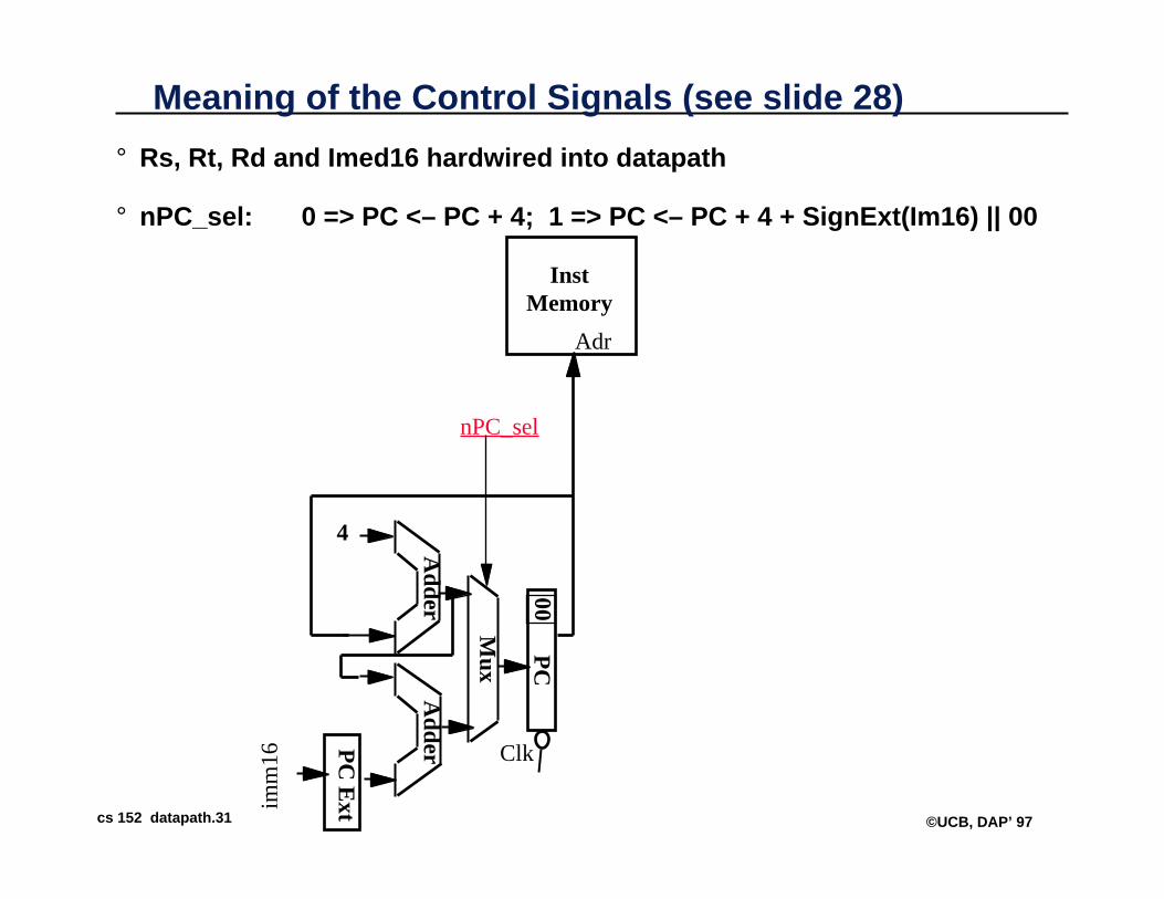
Meaning of the Control Signals (see slide 28)
° Rs, Rt, Rd and Imed16 hardwired into datapath
° nPC_sel: 0 => PC <– PC + 4; 1 => PC <– PC + 4 + SignExt(Im16) || 00
Adder
Adder
PC
Clk
00
Mux
4
nPC_sel
PC
Extim
m16

cs 152 datapath.32 ©UCB, DAP’ 97
Meaning of the Control Signals (see slide 28)
° ExtOp: “zero”, “sign”
° ALUsrc: 0 => regB; 1 => immed
° ALUctr: “add”, “sub”, “or”
32
ALUctr
Clk
busW
RegWr
32
32
busA
32busB
55 5
Rw Ra Rb32 32-bitRegisters
Rs
Rt
Rt
RdRegDst
Extender
Mux
3216imm16
ALUSrcExtOp
Mux
MemtoReg
Clk
Data InWrEn32 Adr
DataMemory
MemWr
AL
U
Equal
0
1
0
1
01
° MemWr: write memory
° MemtoReg: 1 => Mem
° RegDst: 0 => “rt”; 1 => “rd”
° RegWr: write dest register
=

cs 152 datapath.33 ©UCB, DAP’ 97
Control Signalsinst Register Transfer
ADD R[rd] <– R[rs] + R[rt]; PC <– PC + 4
ALUsrc = RegB, ALUctr = “add”, RegDst = rd, RegWr, nPC_sel = “+4”
SUB R[rd] <– R[rs] – R[rt]; PC <– PC + 4
ALUsrc = ___, Extop = __, ALUctr = ___, RegDst = ___, RegWr(?), MemtoReg(?), MemWr(?), nPC_sel =__
ORi R[rt] <– R[rs] + zero_ext(Imm16); PC <– PC + 4
ALUsrc = ___, Extop = __, ALUctr = ___, RegDst = ___, RegWr(?), MemtoReg(?), MemWr(?), nPC_sel =__
LOAD R[rt] <– MEM[ R[rs] + sign_ext(Imm16)]; PC <– PC + 4
ALUsrc = ___, Extop = __, ALUctr = ___, RegDst = ___, RegWr(?), MemtoReg(?), MemWr(?), nPC_sel =__
STORE MEM[ R[rs] + sign_ext(Imm16)] <– R[rs]; PC <– PC + 4
ALUsrc = ___, Extop = __, ALUctr = ___, RegDst = ___, RegWr(?), MemtoReg(?), MemWr(?), nPC_sel =__
BEQ if ( R[rs] == R[rt] ) then PC <– PC + sign_ext(Imm16)] || 00 else PC <– PC + 4
ALUsrc = ___, Extop = __, ALUctr = ___, RegDst = ___, RegWr(?), MemtoReg(?), MemWr(?), nPC_sel =__

cs 152 datapath.34 ©UCB, DAP’ 97
Control Signals
inst Register Transfer
ADD R[rd] <– R[rs] + R[rt]; PC <– PC + 4
ALUsrc = RegB, ALUctr = “add”, RegDst = rd, RegWr, nPC_sel = “+4”
SUB R[rd] <– R[rs] – R[rt]; PC <– PC + 4
ALUsrc = RegB, ALUctr = “sub”, RegDst = rd, RegWr, nPC_sel = “+4”
ORi R[rt] <– R[rs] + zero_ext(Imm16); PC <– PC + 4
ALUsrc = Im, Extop = “Z”, ALUctr = “or”, RegDst = rt, RegWr, nPC_sel = “+4”
LOAD R[rt] <– MEM[ R[rs] + sign_ext(Imm16)]; PC <– PC + 4
ALUsrc = Im, Extop = “Sn”, ALUctr = “add”, MemtoReg, RegDst = rt, RegWr, nPC_sel = “+4”
STORE MEM[ R[rs] + sign_ext(Imm16)] <– R[rs]; PC <– PC + 4
ALUsrc = Im, Extop = “Sn”, ALUctr = “add”, MemWr, nPC_sel = “+4”
BEQ if ( R[rs] == R[rt] ) then PC <– PC + sign_ext(Imm16)] || 00 else PC <– PC + 4
nPC_sel = EQUAL, ALUctr = “sub”

cs 152 datapath.35 ©UCB, DAP’ 97
Step 5: Logic for each control signal
° nPC_sel <= if (OP == BEQ) then EQUAL else 0
° ALUsrc <= if (OP == “000000”) then “regB” else “immed”
° ALUctr <= if (OP == “000000”) then functelseif (OP == ORi) then “OR”elseif (OP == BEQ) then “sub” else “add”
° ExtOp <= _____________
° MemWr <= _____________
° MemtoReg <= _____________
° RegWr: <=_____________
° RegDst: <= _____________

cs 152 datapath.36 ©UCB, DAP’ 97
Step 5: Logic for each control signal
° nPC_sel <= if (OP == BEQ) then EQUAL else 0
° ALUsrc <= if (OP == “000000”) then “regB” else “immed”
° ALUctr <= if (OP == “000000”) then functelseif (OP == ORi) then “OR” elseif (OP == BEQ) then “sub” else “add”
° ExtOp <= if (OP == ORi) then “zero” else “sign”
° MemWr <= (OP == Store)
° MemtoReg <= (OP == Load)
° RegWr: <= if ((OP == Store) || (OP == BEQ)) then 0 else 1
° RegDst: <= if ((OP == Load) || (OP == ORi)) then 0 else 1

cs 152 datapath.37 ©UCB, DAP’ 97
Example: Load Instruction
32
ALUctr
Clk
busW
RegWr
32
32
busA
32busB
55 5
Rw Ra Rb32 32-bitRegisters
Rs
Rt
Rt
RdRegDst
Extender
Mux
3216imm16
ALUSrcExtOp
Mux
MemtoReg
Clk
Data InWrEn32 Adr
DataMemory
MemWrA
LU
Equal
Instruction<31:0>
0
1
0
1
01
<21:25>
<16:20>
<11:15>
<0:15>
Imm16RdRtRs
=
imm
16
Adder
Adder
PC
Clk
00
Mux
4
nPC_sel
PC
Ext
Adr
InstMemory
sign ext
addrt+4

cs 152 datapath.38 ©UCB, DAP’ 97
An Abstract View of the Implementation
° Logical vs. Physical Structure
DataOut
Clk
5
Rw Ra Rb
32 32-bitRegisters
Rd
AL
U
Clk
Data In
DataAddress
IdealData
Memory
Instruction
InstructionAddress
IdealInstruction
Memory
Clk
PC
5Rs
5Rt
32
323232
A
B
Nex
t A
ddre
ss
Control
Datapath
Control Signals Conditions

cs 152 datapath.39 ©UCB, DAP’ 97
A Real MIPS Datapath (CNS T0)

cs 152 datapath.40 ©UCB, DAP’ 97
Summary
° 5 steps to design a processor• 1. Analyze instruction set => datapath requirements
• 2. Select set of datapath components & establish clock methodology
• 3. Assemble datapath meeting the requirements
• 4. Analyze implementation of each instruction to determine setting of control points that effects the register transfer.
• 5. Assemble the control logic
° MIPS makes it easier• Instructions same size
• Source registers always in same place
• Immediates same size, location
• Operations always on registers/immediates
° Single cycle datapath => CPI=1, CCT => long
° Next time: implementing control