cs221: vhdl models synthesis · cs221: vhdl models & synthesis dr. ... how to write fsm is vhdl...
TRANSCRIPT

CS221: VHDL Models & Synthesis
Dr. A. Sahu
Dept of Comp. Sc. & Engg.Dept of Comp. Sc. & Engg.
Indian Institute of Technology Guwahati
1

Outline
• Examples : N Bit Ripple Adder Mux Register FSM– N Bit Ripple Adder, Mux , Register, FSM
• VHDL Model
–Data Flow–Data Flow– Component
– Behavioral ModelBehavioral Model
• VHDL Synthesis
2

N Bit Ripple Carry Adder: FAN Bit Ripple Carry Adder: FAENTITY full_adder IS
PORT (a, b, c_in: IN std_logic; Sum, Carry: OUT std_logic );
END full_adder;
ARCHITECTURE full_adder_arch_1 OF full_adder IS
SIGNAL S1, S2, S3: std_logic;BEGINBEGIN
s3 <= ( a AND b ) after 5 ns;s2 <= ( c_in AND s1 ) after 5 ns;s1 <= ( a XOR b ) after 15 ns; Carry <= ( s2 OR s3 ) after 5 ns;Sum <= ( s1 XOR c in ) after 15 ns;
3
( _ ) ;
END full_adder_arch_1;

N Bit Ripple Carry AdderN Bit Ripple Carry AdderENTITY adder_bits_n IS
GENERIC(n: INTEGER := 2);
PORT (
Cin: IN std_logic;
a, b: IN std_logic_vector(n‐1 downto 0);S: OUT std_logic_vector(n‐1 downto 0);Cout: OUT std logicCout: OUT std_logic);
4
END;

N Bit Ripple Carry AdderN Bit Ripple Carry AdderARCHITECTURE ripple_n_arch OF adder_bits_n IS
COMPONENT full_adderPORT (x, y, z: IN std_logic; Sum, Carry: OUT std_logic);
END COMPONENT;END COMPONENT;
SIGNAL t: std_logic_vector(n downto 0);
BEGIN
t(0) <= Cin; Cout <= t(n);( ) ; ( );
FA: FOR i in 0 to n‐1 GENERATEFA_i: full_adder PORT MAP (t(i), a(i), b(i), S(i), t(i+1));
end generate;
5
end generate;END;

Test benches for 4 bit adder: Stimulus only ARCHITECTURE tb OF tb_adder_4 IS
COMPONENT adder bits n GENERIC(n: INTEGER := 2);COMPONENT adder_bits_n GENERIC(n: INTEGER := 2);PORT ( Cin: IN std_logic; a, b: IN std_logic_vector(n‐1 downto 0);
S: OUT std_logic_vector(n‐1 downto 0); Cout: OUT std_logic); END COMPONENT;END COMPONENT;
SIGNAL x, y, Sum: std_logic_vector(n downto 0);
SIGNAL c Cout: std logic;SIGNAL c, Cout: std_logic;BEGIN
x <= “0000”, “0001” after 200 ns, “0101”, after 400 ns;< “0010” “0011” ft 200 “1010” ft 400y <= “0010”, “0011” after 200 ns, “1010”, after 400 ns;
c <= ‘1’, ‘0’ after 200 ns;UUT_ADDER_4: adder_bits_n GENERIC MAP(4)
PORT MAP ( S C )
6
PORT MAP (c, x, y, Sum, Cout);END

4 bit multiplexor 4x1
4x1
I0
I1
I2Y
4 Bit : 3 downto 04x1 Mux
I2
I3
S1 S0
entityMux is
port( I3: in std_logic_vector(3 downto 0);I2: in std logic vector(3 downto 0);_ g _ ( );
I1: in std_logic_vector(3 downto 0);I0: in std_logic_vector(3 downto 0);S: in std logic vector(1 downto 0);S: in std_logic_vector(1 downto 0);O: out std_logic_vector(3 downto 0)
);
7
endMux;
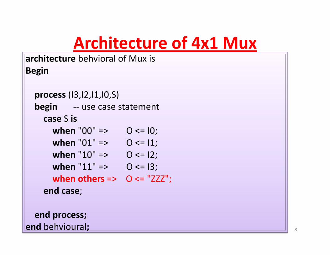
Architecture of 4x1 MuxArchitecture of 4x1 Muxarchitecture behvioral of Mux is
Begin
process (I3,I2,I1,I0,S)begin ‐‐ use case statementg
case S iswhen "00" => O <= I0;when "01" => O <= I1;when 01 => O <= I1;when "10" => O <= I2;when "11" => O <= I3;h h O "ZZZ"when others => O <= "ZZZ";
end case;
8
end process;end behvioural;

Resister i i ientity regis is
port( rst, clk, load: in std_logic;input: in std_logic_vector( 3 downto 0 );output: out std_logic_vector( 3 downto 0 )
);
end regis;end regis;
architecture regis_arc of regis isbegin
( lk l d i )process( rst, clk, load, input )begin
if( rst = '1' ) then output <= "0000";elsif( clk'event and clk = '1') thenif( load = '1' ) then output <= input; end if; end if;
9
end if; end if; end process;
end regis_arc;

How to Write FSM is VHDLHow to Write FSM is VHDL
S301010
S0 S1 S2InitC= 10
C
00000 00011 xxx00
01010
S4
C=
01 C=
11
entity fsm is
S511111
00101
entity fsm is
port( rst, clk,proceed : in std_logic;comparison: in std_logic_vector( 1 downto 0 );
bl l l ld ld t td l i
10
;
enable, xsel, ysel, xld, yld: out std_logic);
end fsm;
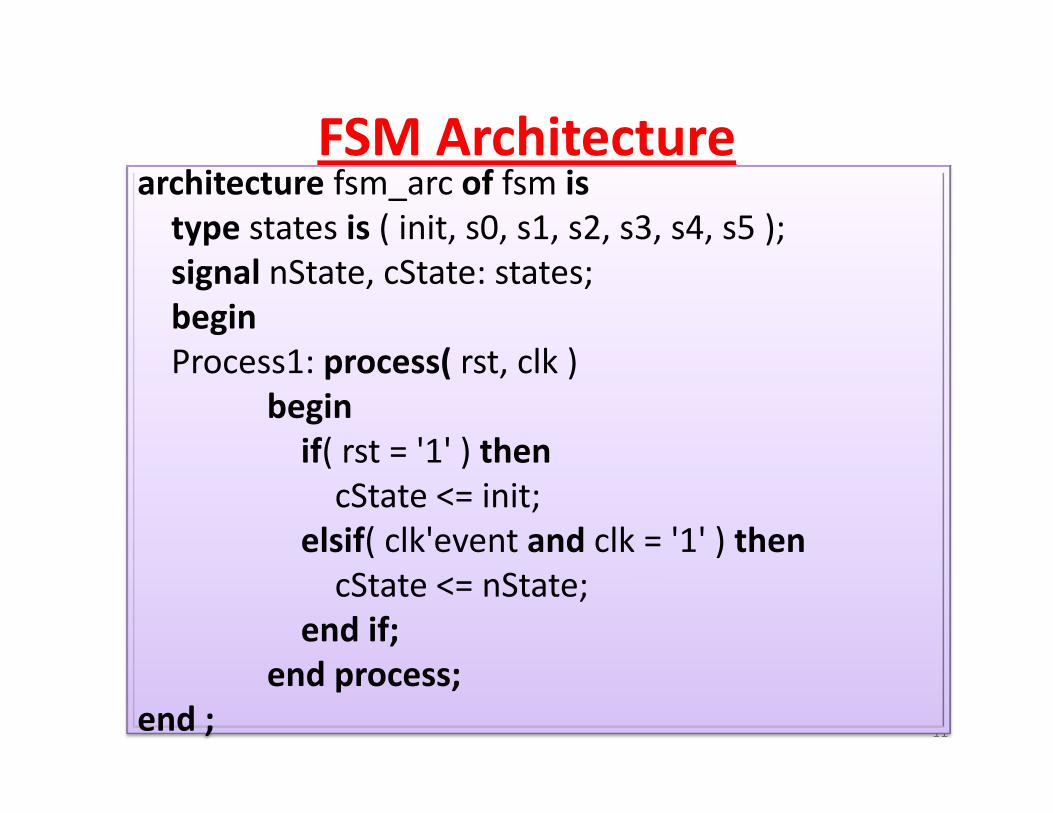
FSM ArchitectureFSM Architecturearchitecture fsm_arc of fsm is
type states is ( init, s0, s1, s2, s3, s4, s5 );signal nState, cState: states;begin
P 1 ( t lk )Process1: process( rst, clk )begin
if( rst = '1' ) thenif( rst 1 ) thencState <= init;
elsif( clk'event and clk = '1' ) thencState <= nState;
end if;d
11
end process;end ;

FSM Architectureprocess( proceed, comparison, cState )begin
variable : OP : std_loic_vector (4 downto 0);case cState iswhen init => if( proceed = '0' ) then nState <= init;
else nState <= s0; end if;when s0 => OP <= “ 00000 “ ; nState <= s1;h 1 > OP < “ 00001” St t < 2when s1 => OP <= “ 00001”; nState <= s2;
when s2 => OP<= “ XXX01” ; if( comparison = "10" ) then nState <= s3;
elsif( comparison = "01" ) then nState <= s4;elsif( comparison = 01 ) then nState <= s4;elsif( comparison = "11" ) then nState <= s5; end if;
when s3 => OP <= “ 01010” nState <= s2;when s4 => OP <= “ 00101” ; nState <= s2;; ;
when s5 => OP <= “11111” ; nState <= s0;when others => nState <= s0;end case;
12
enable <= OP(4); xsel <= OP(3);ysel <= OP(2);xld <= OP(1);yld <= OP(0);end process;
end fsm_arc;

Data Flow: Full AdderData Flow: Full AdderENTITY full_adder IS
PORT (a, b, c_in: IN std_logic; Sum, Carry: OUT std_logic );
END full_adder;
ARCHITECTURE Data_Flow OF full_adder IS
SIGNAL S1, S2, S3: std_logic;BEGINBEGIN
s3 <= ( a AND b ) after 5 ns;s2 <= ( c_in AND s1 ) after 5 ns;s1 <= ( a XOR b ) after 15 ns; Carry <= ( s2 OR s3 ) after 5 ns;Sum <= ( s1 XOR c in ) after 15 ns;
13
( _ ) ;
END full_adder_arch_1;

Components : FAArchitecture structural of Full adder isArchitecture structural of Full_adder iscomponent XOR_GATE is
port( X, Y : in std_logic; F2: out std_logic );
end component;
component AND_GATE is port( X, Y : in std logic; F2: out std logic );p ( , _ g ; _ g );
end component;
component OR_GATE is ……..signal s1 s2 s3: std logic; signal just like wiresignal s1, s2.s3: std_logic; ‐‐ signal just like wire
Begin
XOR1: XOR_GATE port map (a, b, s1);AND1: AND_GATE port map (a, b , s3);AND2 : AND_GATE port map(c_in, s1, s2);OR1 : OR GATE port map (s2,s3, Carry);
14
_ p p ( , , y);
XOR2: XOR_GATE port map (s1,c_in, Sum);
end structural;

Behavioral Model architecture BEHAV FA of FULL ADDER isarchitecture BEHAV_FA of FULL_ADDER issignal int1, int2, int3: std_logic;Begin ‐‐ Process P1 that defines the first half adderP1 (A B)P1: process (A, B)
begin
int1<= A xor B;int2<= A and B;
end process;‐‐ Process P2 that defines the second half adder and the OR ‐‐ gateProcess P2 that defines the second half adder and the OR gate
P2: process (int1, int2, Cin)begin
S < i t1 or CiSum <= int1 xor Cin;int3 <= int1 and Cin;Cout <= int2 or int3;
15
end process;end BEHAV_FA;

Hardware SpecificationHardware Specification
• Layout editor – directly enter layout– Up to ~102 of unique transistors– Complex circuitsComplex circuits– Memory, aided by generators
• Schematic Capturea
b– Enter gates and interconnections– Up to ~104 transistors
• Hardware Description Languages
bF
Hardware Description Languages– Enter text description– 107 transistors
Entity ..If (x < y) then Y=x and z;
16
Y=x and z;….

Hardware SpecificationComplexity Maintainability
and Modifiability
Optimal Efficiency
a
bF
E titEntity ..If (x < y) then Y=x and z;….

IC Design ProcessIC Design Process
Id
D i F b i ti T ti P k i
IdeaLayout
Die Tested Die
Design Fabrication Testing Packaging
SpecificationSpecification
Implementation
Model
Synthesis
Verification & Simulation
18

Hardware/Software Design FlowHardware/Software Design Flow
HW SW
Specification
Synthesis
Specification
Compilation
Layout
Fabrication
Binary Code
IC
Fabrication
19

ModelModel
• Representation of abstract view of the SystemRepresentation of abstract view of the System
• Varying abstractionsf ti l l– functional only
– timing only
– functional + timing
20

Modelling: level of detailModelling: level of detail• Behavioral Level for (i=0;i <4;i++)
S S A[i]– no clock cycle level commitment
• Register‐Transfer Level (RTL)
S = S+ A[i]
– Operations committed to clock cycles
Cycle 1: T1 = A[0] + A[1]Cycle 1: T1 = A[0] + A[1]T2 = A[2] + A[3]
Cycle 2: S = T1 + T2
• Gate level– structural netlist
21

SynthesisSynthesis
• HDL → Layout
Entity ..If (x < y) then Y dHDL → Layout
– HDL → Gates
Gates → Layout
Y=x and z;….
– Gates → Layouta
bHW
Specification
bF
Layout
Synthesis
22

SynthesisSynthesis
• Behavioral Synthesis (Process & Sequential )Behavioral Synthesis (Process & Sequential )– Behavioral HDL → RTL HDL
No notion of clock to Clocked– No notion of clock to Clocked
• RTL Synthesis – RTL HDL → Gates
• Layout Synthesis– Gates → Layout
23
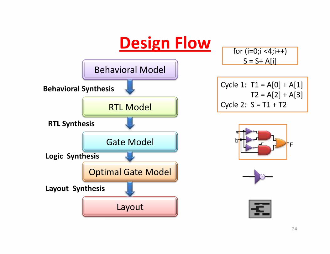
Design FlowDesign FlowBehavioral Model
for (i=0;i <4;i++)S = S+ A[i]
RTL Model
Cycle 1: T1 = A[0] + A[1]T2 = A[2] + A[3]
Cycle 2: S = T1 + T2
Behavioral Synthesis
Gate Model
ab
F
RTL Synthesis
Gate Model
Optimal Gate Model
F
Logic Synthesis
Optimal Gate Model
Layout
Layout Synthesis
24
Layout

25