cs4350 - farnell element14 · 2 ds691pp1 cs4350 description the cs4350 is a complete stereo...
TRANSCRIPT

CS4350
192 kHz Stereo DAC with Integrated PLLFeaturesAdvanced Multi-bit Delta-Sigma Architecture109 dB Dynamic Range-91 dB THD+N24-Bit ConversionSupports Audio Sample Rates Up to 192 kHz Low-Latency Digital FilteringSingle-Ended or Differential Analog Output ArchitectureIntegrated PLL Locks to Incoming Left-Right Clock – Eliminates the Need for External Master-
clock Routing– Reduces Interference and Jitter Sensitivity– No External Loop Filter Components
RequiredAutomatic Sample-Rate Range Detection
Popguard® Technology for Control of Clicks and Pops– Hardware Popguard Disable for Fast
Startups
Supports All Standard Serial Audio Formats Including Time-Division Multiplexed (TDM)+1.5 V to 5.0 V Logic Supplies for Serial Port+3.3 V to 5.0 V Control Port Interface
Control Port Mode FeaturesSPI™ and I²C® ModesATAPI MixingMute Control for Individual ChannelsDigital Volume Control with Soft Ramp– 127.5 dB Attenuation– 1/2 dB Step Size– Zero Crossing Click-Free Transitions
PCMSerial
Interface
Serial Audio Input
Right Channel Output
Left Channel Output
Reset
3.3 V to 5.0 VRegister/Hardware
ConfigurationHardware or I2C/SPI Control Data
3.3 V to 5.0 V
LRCK RM
CK
RMCKRecovered MCLK
1.5 V to 5.0 V
Internal VoltageReference
and RegulationPhase Locked Loop
InterpolationFilter withVolume Control
InterpolationFilter withVolume Control
Multibit ΔΣModulator
Multibit ΔΣModulator
Leve
l Tra
nsla
tor
Leve
l Tra
nsla
tor
Amp+
Filter
Amp+
Filter
Left and Right Mute Controls
ExternalMute
Control
DAC
DAC
Copyright © Cirrus Logic, Inc. 2007(All Rights Reserved)http://www.cirrus.com
Preliminary Product Information This document contains information for a new product. Cirrus Logic reserves the right to modify this product without notice.
MARCH '07DS691PP1

CS4350
DescriptionThe CS4350 is a complete stereo digital-to-analog system including PLL-based master clock derivation, digital in-terpolation, 5th-order multi-bit delta-sigma digital-to-analog conversion, digital de-emphasis, volume control,channel mixing, and analog filtering. The advantages of this architecture include ideal differential linearity, no dis-tortion mechanisms due to resistor matching errors, no linearity drift over time and temperature, high tolerance toclock jitter, and a minimal set of external components.
The CS4350 supports all standard digital audio interface formats, including TDM.
The CS4350 is available in a 24-pin TSSOP package in both Commercial (-40° to +85°C) and Automotive grades(-40° to +105°C). The CDB4350 Customer Demonstration board is also available for device evaluation and imple-mentation suggestions. Please refer to “Ordering Information” on page 40 for complete ordering information.
These features are ideal for cost-sensitive, 2-channel audio systems, including DVD players and recorders, set-topboxes, digital TVs, mini-component systems, mixing consoles and automotive audio systems.
2 DS691PP1

CS4350
TABLE OF CONTENTS1. PIN DESCRIPTION.................................................................................................................................. 62. CHARACTERISTICS AND SPECIFICATIONS....................................................................................... 8RECOMMENDED OPERATING CONDITIONS .......................................................................................... 8ABSOLUTE MAXIMUM RATINGS............................................................................................................... 8DAC ANALOG CHARACTERISTICS - COMMERCIAL (-CZZ) ................................................................... 9DAC ANALOG CHARACTERISTICS - AUTOMOTIVE (-DZZ) .................................................................. 10COMBINED INTERPOLATION & ON-CHIP ANALOG FILTER RESPONSE............................................ 12SWITCHING SPECIFICATIONS - SERIAL AUDIO INTERFACE.............................................................. 13SWITCHING CHARACTERISTICS - CONTROL PORT - I²C FORMAT.................................................... 14SWITCHING CHARACTERISTICS - CONTROL PORT - SPI FORMAT................................................... 15DIGITAL CHARACTERISTICS .................................................................................................................. 16POWER AND THERMAL CHARACTERISTICS........................................................................................ 163. TYPICAL CONNECTION DIAGRAM .................................................................................................. 174. APPLICATIONS .................................................................................................................................... 18
4.1 Sample Rate Range and Oversampling Mode Detect................................................................... 184.1.1 Sample Rate Auto-Detect .................................................................................................... 18
4.2 System Clocking............................................................................................................................ 184.2.1 Recovered Master Clock (RMCK)........................................................................................ 18
4.3 Digital Interface Format ................................................................................................................. 194.3.1 Time-Division Multiplex (TDM) Mode ................................................................................... 20
4.4 De-Emphasis ................................................................................................................................. 214.5 Mute Control .................................................................................................................................. 214.6 Recommended Power-Up Sequence ............................................................................................ 21
4.6.1 Stand-Alone Mode ............................................................................................................... 214.6.2 Control Port Mode ................................................................................................................ 22
4.7 Popguard Transient Control .......................................................................................................... 224.7.1 Power-Up ............................................................................................................................. 224.7.2 Power-Down......................................................................................................................... 224.7.3 Discharge Time .................................................................................................................... 22
4.8 Analog Output and Filtering........................................................................................................... 234.9 Grounding and Power Supply Arrangements ................................................................................ 23
4.9.1 Capacitor Placement............................................................................................................ 235. STAND-ALONE OPERATION............................................................................................................... 24
5.1 Serial Port Format Selection.......................................................................................................... 245.2 De-Emphasis Control .................................................................................................................... 245.3 Popguard Transient Control .......................................................................................................... 24
6. CONTROL PORT OPERATION ............................................................................................................ 256.1 MAP Auto Increment ..................................................................................................................... 256.2 I²C Mode........................................................................................................................................ 25
6.2.1 I²C Write ............................................................................................................................... 256.2.2 I²C Read............................................................................................................................... 25
6.3 SPI Mode....................................................................................................................................... 266.3.1 SPI Write .............................................................................................................................. 266.3.2 SPI Read.............................................................................................................................. 27
6.4 Memory Address Pointer (MAP) ................................................................................................... 276.4.1 INCR (Auto Map Increment Enable) .................................................................................... 276.4.2 MAP (Memory Address Pointer) .......................................................................................... 27
7. REGISTER QUICK REFERENCE ......................................................................................................... 288. REGISTER DESCRIPTION ................................................................................................................... 29
8.1 Device and Revision ID - Register 01h.......................................................................................... 298.2 Mode Control - Register 02h ......................................................................................................... 29
8.2.1 Digital Interface Format (DIF[2:0]) Bits 6-4 .......................................................................... 29
DS691PP1 3

CS4350
8.2.2 De-Emphasis Control (DEM[1:0]) Bits 3-2 ........................................................................... 308.2.3 Functional Mode (FM[1:0]) Bits 1-0...................................................................................... 308.3 Volume Mixing and Inversion Control - Register 03h .................................................................... 308.3.1 Channel A Volume = Channel B Volume (VOLB=A) Bit 7 ................................................... 308.3.2 Invert Signal Polarity (INVERT_A) Bit 6 ............................................................................... 308.3.3 Invert Signal Polarity (INVERT_B) Bit 5 ............................................................................... 318.3.4 ATAPI Channel Mixing and Muting (ATAPI[3:0]) Bits 3-0 .................................................... 31
8.4 Mute Control - Register 04h ......................................................................................................... 328.4.1 Auto-Mute (AMUTE) Bit 7 .................................................................................................... 328.4.2 AMUTEC = BMUTEC (MUTEC A=B) Bit 5 .......................................................................... 328.4.3 Channel A Mute (MUTE_A) Bit 4 & Channel B Mute (MUTE_B) Bit 3................................. 32
8.5 Channel A & B Volume Control - Register 05h & 06h ................................................................... 338.6 Ramp and Filter Control - Register 07h......................................................................................... 33
8.6.1 Soft Ramp and Zero Cross Control (SZC[1:0]) Bits 7-6 ....................................................... 338.6.2 Soft Volume Ramp-Up after Error (RMP_UP) Bit 5 ............................................................. 348.6.3 Soft Ramp-Down before Filter Mode Change (RMP_DN) Bit 4 ........................................... 348.6.4 Interpolation Filter Select (FILT_SEL) Bit 2.......................................................................... 34
8.7 Misc. Control - Register 08h .......................................................................................................... 348.7.1 Power Down (PDN) Bit 7...................................................................................................... 348.7.2 Freeze Controls (FREEZE) Bit 5.......................................................................................... 358.7.3 Popguard Enable (POPG_EN) Bit 4 .................................................................................... 358.7.4 RMCK control (RMCK_CTR[1:0]) Bits 3:2 ........................................................................... 358.7.5 RMCK Ratio Select (R_SELECT[1:0]) Bits 2:1 .................................................................... 35
9. FILTER PLOTS .................................................................................................................................. 3610. PARAMETER DEFINITIONS............................................................................................................... 3811. PACKAGE DIMENSIONS ................................................................................................................... 39THERMAL CHARACTERISTICS............................................................................................................... 3912. ORDERING INFORMATION ............................................................................................................... 4013. REVISION HISTORY .......................................................................................................................... 40
4 DS691PP1

CS4350
LIST OF FIGURESFigure 1. Equivalent Output Load .............................................................................................................. 11Figure 2. Maximum Loading....................................................................................................................... 11Figure 3. Serial Port Timing, Non-TDM Mode............................................................................................ 13Figure 4. Serial Port Timing, TDM Mode.................................................................................................... 13Figure 5. Control Port Timing - I²C Format................................................................................................. 14Figure 6. Control Port Timing - SPI Mode .................................................................................................. 15Figure 7. Typical Connection Diagram....................................................................................................... 17Figure 8. Left-Justified up to 24-Bit Data.................................................................................................... 19Figure 9. I²S, up to 24-Bit Data .................................................................................................................. 19Figure 10. Right-Justified Data................................................................................................................... 19Figure 11. TDM Mode Connection Diagram .............................................................................................. 20Figure 12. TDM Mode Timing .................................................................................................................... 20Figure 13. De-Emphasis Curve.................................................................................................................. 21Figure 14. Differential to Single-ended Output Filter.................................................................................. 23Figure 15. Passive Single-Ended Output Filter .......................................................................................... 23Figure 16. Control Port Timing, I²C Mode .................................................................................................. 26Figure 17. Control Port Timing, SPI Mode ................................................................................................. 27Figure 18. De-Emphasis Curve.................................................................................................................. 30Figure 19. ATAPI Block Diagram ............................................................................................................... 31Figure 20. Stopband Rejection (fast), all Modes ........................................................................................ 36Figure 21. Stopband Rejection (slow), all Modes....................................................................................... 36Figure 22. Single-Speed (fast) Passband Detail ........................................................................................ 36Figure 23. Single-Speed (slow) Passband Detail....................................................................................... 36Figure 24. Double-Speed (fast) Passband Detail....................................................................................... 36Figure 25. Double-Speed (slow) Passband Detail ..................................................................................... 36Figure 26. Quad-Speed (fast) Passband Detail ......................................................................................... 37Figure 27. Quad-Speed (slow) Passband Detail........................................................................................ 37
LIST OF TABLESTable 1. Pin Descriptions ............................................................................................................................. 7Table 2. CS4350 Auto-Detect .................................................................................................................... 18Table 3. Digital Interface Format - Stand-Alone Mode............................................................................... 24Table 4. Digital Interface Formats .............................................................................................................. 29Table 5. ATAPI Decode ............................................................................................................................. 31Table 6. Example Digital Volume Settings ................................................................................................. 33
DS691PP1 5

CS4350
1. PIN DESCRIPTIONDIF2(AD1/CDOUT) RST
DEM(AD0/CS) AOUTB-
DIF0(SDA/CDIN) AOUTB+
DIF1(SCL/CCLK) BMUTEC
VLC VQ
VD_FILT GND
GND VA
RMCK VBIAS+
VLS AMUTEC
SCLK AOUTA+
SDIN AOUTA-
LRCK TSTO
2345678 17
181920212223
910
1112 13
141516
241
6 DS691PP1

CS4350
Pin Name # Pin DescriptionVLC 5 Control Interface Power (Input) - Positive power for the hardware/software control interface
VD_FILT 6 Regulator Voltage (Output) - Filter connection for internal voltage regulator
GND 7, 19 Ground (Input) - Ground reference
RMCK 8 Recovered Master Clock (Output) - Outputs a master clock derived from LRCK
VLS 9 Serial Audio Interface Power (Input) - Positive power for the serial audio interface
SCLK 10 Serial Clock (Input) - Serial bit-clock for the serial audio interface
SDIN 11 Serial Audio Data Input (Input) - Input for two’s complement serial audio data
LRCK 12Left/Right Clock (Input) - Determines which channel, Left or Right, is currently active on the serial audio data line
TSTO 13 Test Output - These pins need to be floating and not connected to any trace or plane.
AOUTA+,- AOUTB+,-
14, 15, 22, 23
Differential Analog Outputs (Output) - The full scale differential output level is specified in “DAC Ana-log Characteristics - Commercial (-CZZ)” on page 9.
AMUTECBMUTEC 16, 21 Mute Control (Output) - Control signals for optional mute circuit.
VBIAS 17 Positive Voltage Reference (Output) - Positive reference voltage for the internal DAC
VA 18 Analog Power (Input) - Positive power supply for the analog section
VQ 20 Quiescent Voltage (Output) - Filter connection for internal quiescent voltage
RST 24Reset (Input) - When pulled low, device will power down and reset all internal registers to their default settings.
Control Port Definitions
AD1/CDOUT 1 Address Bit 1 / Serial Control Data Out (I/O) - Chip address bit 1 in I²C Mode or data output in SPI Mode
AD0/CS 2 Address Bit 0 / Chip Select (Input) - Chip address bit 0 in I²C Mode or Chip Select in SPI Mode
SDA/CDIN 3 Serial Control Data In (I/O) - Input/Output for I²C data. Input for SPI data
SCL/CCLK 4 Serial Control Port Clock (Input) - Serial clock for the control port interface
Stand-Alone DefinitionsDIF0DIF1DIF2
1, 3, 4Digital Interface Format (Input) - Defines the required relationship between the Left Right Clock, Serial Clock, and Serial Audio Data
DEM 2De-emphasis (Input) - Selects the standard 15 μs/50 μs digital de-emphasis filter response for 44.1 kHz sample rates
Table 1. Pin Descriptions
DS691PP1 7

CS4350
2. CHARACTERISTICS AND SPECIFICATIONSRECOMMENDED OPERATING CONDITIONSGND = 0 V; all voltages with respect to ground.
ABSOLUTE MAXIMUM RATINGSGND = 0 V; all voltages with respect to ground.(Note 1)
Notes: 1. Operation beyond these limits may result in permanent damage to the device. Normal operation is not guaranteed at these extremes.
2. Any pin except supplies.
Parameters Symbol Min Typ Max UnitsDC Power Supply Analog power VA 4.75 5.0 5.25 V
3.14 3.3 3.46 V
Serial Audio Interface power VLS 1.35 3.3 5.25 V
Control Interface power VLC 3.14 3.3 5.25 VAmbient Operating Temperature (Power Applied)
Commercial (-CZZ) TA -40 - +85 °CAutomotive (-DZZ) TA -40 - +105 °C
Parameters Symbol Min Max UnitsDC Power Supply Analog power VA -0.3 6.0 V
Serial Audio Interface power VLS -0.3 6.0 V
Control Interface power VLC -0.3 6.0 VInput Current (Note 2) Iin - ±10 mADigital Input Voltage Serial Audio Interface VIN-LS -0.3 VLS+ 0.4 VControl Interface VIN-LC -0.3 VLC+ 0.4 VAmbient Operating Temperature (power applied) TA -55 125 °CStorage Temperature Tstg -65 150 °C
8 DS691PP1

CS4350
DAC ANALOG CHARACTERISTICS - COMMERCIAL (-CZZ)Test conditions (unless otherwise specified): VLS = VLC = 3.3 V; TA = 25° C; input test signal is a 997 Hz sine wave; Valid with the recommended capacitor values on VFILT, VQ, and VBIAS and output circuit as shown in the typical con-nection diagram in Figure 7; Fs = 48 kHz, 96 kHz, and 192 kHz; measurement bandwidth 10 Hz to 20 kHz.Note: 1. One-half LSB of triangular PDF dither is added to data2. RL and CL represent the minimum resistance and maximum capacitance required for the CS4350’s internal op-amp
to remain stable. See Figure 1 and Figure 2 for more details.
Parameter Symbol Min Typ Max UnitVA=+5 V Single-ended/Differential
Dynamic Range (Note 1) 24-bit A-Weightedunweighted
16-bit A-Weighted unweighted
95/10392/100
--
101/10998/10695/9692/93
----
dBdBdBdB
Total Harmonic Distortion + Noise (Note 1) 24-bit 0 dB
-20 dB-60 dB
16-bit 0 dB -20 dB
-60 dB
THD+N
-------
-91-78/-86-38/-46
-90-72/-73-32/-33
-85-
-32/-40---
dBdBdBdBdBdB
VA=+3.3 V Single-ended/DifferentialDynamic Range (Note 1) 24-bit A-Weighted
unweighted16-bit A-Weighted
unweighted
95/10392/100
--
101/10998/10695/9692/93
----
dBdBdBdB
Total Harmonic Distortion + Noise (Note 1) 24-bit 0 dB
-2 dB-20 dB-60 dB
16-bit 0 dB -20 dB
-60 dB
THD+N
-------
-84-91/-93-78/-86-38/-46
-83-72/-73-32/-33
-76--
-32/-40---
dBdBdBdBdBdBdB
VA=+5 to+3.3 V Interchannel Isolation (1 kHz) - 100 - dBDC AccuracyInterchannel Gain Mismatch - 0.1 0.25 dBGain Drift - -400 - ppm/°CAnalog OutputFull Scale Output Voltage - Single Ended 2.55 2.78 3.02 VppFull Scale Output Voltage - Differential 5.10 5.56 6.04 VppQuiescent Voltage VQ - 0.5•VA - VDCMax DC Current draw from an AOUT pin IOUTmax - 10 - μAMax Current draw from VQ IQmax - 100 - μAMax AC-Load Resistance (Note 2) RL - 3 - kΩMax Load Capacitance (Note 2) CL - 100 - pFOutput Impedance ZOUT - 100 - Ω
DS691PP1 9

CS4350
DAC ANALOG CHARACTERISTICS - AUTOMOTIVE (-DZZ)Test conditions (unless otherwise specified): VLS = 1.35 V to 5.25 V, VLC = 3.14 V to 5.25 V, TA = -40° C to 85° C, input test signal is a 997 Hz sine wave; Valid with the recommended capacitor values on VFILT, VQ, and VBIAS and output circuit as shown in the typical connection diagram in Figure 7; Fs = 48 kHz, 96 kHz, and 192 kHz; measurement band-width 10 Hz to 20 kHz.Parameter Symbol Min Typ Max UnitVA=+4.75 V to +5.25 V Single-ended/Differential
Dynamic Range (Note 1) 24-bit A-Weightedunweighted
16-bit A-Weighted unweighted
95/10392/100
--
101/10998/10695/9692/93
----
dBdBdBdB
Total Harmonic Distortion + Noise (Note 1) 24-bit 0 dB
-20 dB-60 dB
16-bit 0 dB -20 dB
-60 dB
THD+N
-------
-91-78/-86-38/-46
-90-72/-73-32/-33
-85-
-32/-40---
dBdBdBdBdBdB
VA=+3.14 V to +3.46 V Single-ended/DifferentialDynamic Range (Note 1) 24-bit A-Weighted
unweighted16-bit A-Weighted
unweighted
95/10391/100
--
101/10998/10695/9692/93
----
dBdBdBdB
Total Harmonic Distortion + Noise (Note 1) 24-bit 0 dB
-2 dB-20 dB-60 dB
16-bit 0 dB -20 dB
-60 dB
THD+N
-------
-84-91/-93-78/-86-38/-46
-83-72/-73-32/-33
-74--
-31/-40---
dBdBdBdBdBdBdB
VA=+3.14 to+5.25 V Interchannel Isolation (1 kHz) - 100 - dBDC AccuracyInterchannel Gain Mismatch - 0.1 0.25 dBGain Drift - -400 - ppm/°CAnalog OutputFull Scale Output Voltage - Single Ended 2.48 2.78 3.08 VppFull Scale Output Voltage - Differential 4.96 5.56 6.16 VppQuiescent Voltage VQ - 0.5•VA - VDCMax DC Current draw from an AOUT pin IOUTmax - 10 - μAMax Current draw from VQ IQmax - 100 - μAMax AC-Load Resistance (Note 2) RL - 3 - kΩMax Load Capacitance (Note 2) CL - 100 - pFOutput Impedance ZOUT - 100 - Ω
10 DS691PP1

CS4350
AOUTx +3.3 µF
Analog Output
+
CS4350
AGND
RL CL
100
50
75
25
2.5 5 10 15
Safe OperatingRegion
Cap
aciti
ve L
oad
-- C
(p
F)L
Resistive Load -- R (kΩ )L
125
320
Figure 1. Equivalent Output Load Figure 2. Maximum Loading
DS691PP1 11

CS4350
COMBINED INTERPOLATION & ON-CHIP ANALOG FILTER RESPONSEThe filter characteristics have been normalized to the sample rate (Fs) and can be referenced to the desired sam-ple rate by multiplying the given characteristic by Fs. Amplitude vs. Frequency plots of this data are available in the “Filter Plots” on page 36Notes: 3. Response is clock dependent.4. The Measurement Bandwidth is from stopband to 3 Fs.5. De-emphasis is available only in Single-Speed Mode; Only 44.1 kHz De-emphasis is available in Stand-Alone
Mode.6. Slow Roll-off interpolation filter is only available in Control Port Mode.
Parameter Min Typ Max UnitFast Roll-Off
Passband (Note 3) -0.01 dB corner (Single Speed) 0 - .454 Fs-0.1 dB corner (Double Speed) 0 - .42 Fs
-0.2 dB corner (Quad Speed) 0 - .27 Fs-3 dB corner (All Speed Modes) 0 - .499 Fs
Frequency Response 10 Hz to 20 kHz Single Speed -0.01 - +0.01 dBDouble Speed, Quad Speed -0.02 - +0.02 dB
StopBand 0.547 - - FsStop-Band Attenuation (Note 4) 102 - - dBTotal Group Delay (Fs = Output Sample Rate) - 9.4/Fs - sIntra-channel Phase Deviation - - ±0.56/Fs sInter-channel Phase Deviation - - 0 sDe-emphasis Error (Note 5) Fs = 32 kHz - - ±0.23 dB(Relative to 1 kHz) Fs = 44.1 kHz - - ±0.14 dB
Fs = 48 kHz - - ±0.09 dB
Slow Roll-Off (Note 6)Passband (Note 3) -0.01 dB corner (Single Speed) 0 - 0.417 Fs
-0.1 dB corner (Double Speed) 0 - .37 Fs-0.2 dB corner (Quad Speed) 0 - .27 Fs
-3 dB corner (All Speed Modes) 0 - .499 FsFrequency Response 10 Hz to 20 kHz Single Speed -0.01 - +0.01 dB
Double Speed, Quad Speed -0.02 - +0.02 dBStopBand .583 - - FsStop-Band Attenuation (Note 4) 64 - - dBTotal Group Delay (Fs = Output Sample Rate) - 6.5/Fs - sIntra-channel Phase Deviation - - ±0.14/Fs sInter-channel Phase Deviation - - 0 sDe-emphasis Error (Note 5) Fs = 32 kHz - - ±0.23 dB(Relative to 1 kHz) Fs = 44.1 kHz - - ±0.14 dB
Fs = 48 kHz - - ±0.09 dB
12 DS691PP1

CS4350
SWITCHING SPECIFICATIONS - SERIAL AUDIO INTERFACEInputs: Logic 0 = GND; Logic 1 = VLS; CL = 20 pFNotes: 7. RMCK output frequency depends on the input LRCK frequency. See Section 4.1 and Section 4.2 for more details.
Parameters Symbol Min Max UnitsRMCK Output Frequency (Note 7) 7.680 55.3 MHz
RMCK Output Duty Cycle 45 55 %
Input Sample Rate Single-Speed Mode Fs 30 54 kHz
Double-Speed Mode Fs 60 108 kHz
Quad-Speed Mode Fs 120 216 kHz
LRCK Duty Cycle (Non-TDM Mode) 40 60 %
SCLK Frequency - 55.3 MHz
SCLK High Time tsckh 11 - ns
SCLK Low Time tsckl 11 - ns
SDIN Setup Time Before SCLK Rising Edge tds 3 - ns
SDIN Hold Time After SCLK Rising Edge tdh 5 - ns
Non-TDM Mode (refer to Figure 3)
LRCK Edge to SCLK Rising Edge tlcks 16 - ns
SCLK Rising Edge to LRCK Edge tlckd 5 - ns
TDM Mode (refer to Figure 4)
LRCK High Time tlrckh 163 ns
SCLK Rising to LRCK Falling Edge tfsh 8 - ns
LRCK Rising Edge to SCLK Rising Edge tfss 5 - ns
tds
LRCK(Input)
tdh
tsclkh tsclkltfshtfss
SCLK(Input)
SDIN(Input)
MSB MSB-1
tlrckh
tds
MSB
tdh
MSB-1
LRCK(input)
SCLK(input)
SDIN(input)
tsckh tsckltlckstlckd
Figure 3. Serial Port Timing, Non-TDM Mode Figure 4. Serial Port Timing, TDM Mode
DS691PP1 13

CS4350
SWITCHING CHARACTERISTICS - CONTROL PORT - I²C FORMATInputs: Logic 0 = GND; Logic 1 = VLC; CL = 20 pF.Notes: 8. Data must be held for sufficient time to bridge the transition time, tfc, of SCL.
Parameter Symbol Min Max UnitSCL Clock Frequency fscl - 100 kHzRST Rising Edge to Start tirs 500 - nsBus Free Time Between Transmissions tbuf 4.7 - µsStart Condition Hold Time (prior to first clock pulse) thdst 4.0 - µsClock Low time tlow 4.7 - µsClock High Time thigh 4.0 - µsSetup Time for Repeated Start Condition tsust 4.7 - µsSDA Hold Time from SCL Falling (Note 8) thdd 0 - µsSDA Setup time to SCL Rising tsud 250 - nsRise Time of SCL and SDA trc, trc - 1 µsFall Time SCL and SDA tfc, tfc - 300 nsSetup Time for Stop Condition tsusp 4.7 - µsAcknowledge Delay from SCL Falling tack 300 1000 ns
t buf t hdst
tlow
thdd
t high
t sud
Stop Start
SDA
SC L
t irs
RST
t hdst
t rc
t fc
t sust
t susp
Start StopRepeated
t rd t fd
t ack
Figure 5. Control Port Timing - I²C Format
14 DS691PP1

CS4350
SWITCHING CHARACTERISTICS - CONTROL PORT - SPI FORMAT Inputs: Logic 0 = GND; Logic 1 = VLC; CL = 20 pFNotes: 9. tspi only needed before first falling edge of CS after RST rising edge. tspi = 0 at all other times.10. Data must be held for sufficient time to bridge the transition time of CCLK.11. For FSCK < 1 MHz.12. CDOUT should not be sampled during this time.
Figure 6. Control Port Timing - SPI Mode
Parameter Symbol Min Max UnitCCLK Clock Frequency fsclk - 6 MHz
RST Rising Edge to CS Falling tsrs 500 - ns
CCLK Edge to CS Falling (Note 9) tspi 500 - ns
CS High Time Between Transmissions tcsh 1.0 - µs
CS Falling to CCLK Edge tcss 20 - ns
CCLK Low Time tscl 66 - ns
CCLK High Time tsch 66 - ns
CDIN to CCLK Rising Setup Time tdsu 40 - ns
CCLK Rising to DATA Hold Time (Note 10) tdh 15 - ns
Rise Time of CCLK and CDIN (Note 11) tr2 - 100 ns
Fall Time of CCLK and CDIN (Note 11) tf2 - 100 ns
Transition Time from CCLK to CDOUT Valid (Note 12) tscdov - 100 ns
Time from CS rising to CDOUT High-Z tcscdo - 100 ns
t r2 t f2
t dsu t dh
t scht scl
CS
CCLK
CDIN
t css t csht spi
t srsRST
CDOUT
t scdov t scdov t cscdo
Hi-Impedance
DS691PP1 15

CS4350
DIGITAL CHARACTERISTICSPOWER AND THERMAL CHARACTERISTICS
Notes: 13. Current consumption increases with increasing Fs within the range of a speed mode. Typ and Max values arebased on highest Fs within a speed mode. Variance between speed modes is small.
14. ILS measured with no external loading on pin 7 (RMCK).15. ILC measured with no external loading on pin 2 (SDA).16. Power-down mode is defined as RST pin = Low with all clock and data lines held static. 17. Valid with the recommended capacitor values on VFILT, VQ, and VBIAS+ as shown in the typical connection dia-
gram in Figure 7.
Parameters Symbol Min Typ Max UnitsHigh-Level Input Voltage VLC or VLS = 5.0 V VIH 0.7•VL - - V
VLC or VLS = 3.3 V VIH 2.0 - - V
VLS = 2.5 V VIH 1.7 - - V
VLS = 1.5 V VIH 0.7•VL - - VHigh-Level Input Voltage VLC or VLS = 5.0 V VIL - - 0.35•VL V
VLC or VLS = 3.3 V VIL - - 0.8 V
VLS = 2.5 V VIL - - 0.7 V
VLS = 1.5 V VIL - - 0.25•VL VInput Leakage Current Iin - - ±10 μAInput Capacitance - 8 - pF
High Level Output Voltage (RMCK) IO = 2 mA (VLS ≥ 3.0V) VOH VLS-1.0 - - V
Low Level Output Voltage (RMCK) IO = -2 mA (VLS ≥ 3.0V) VOL - - 0.4 V
RMCK Output Load Drive - - 10 pFMaximum MUTEC Drive Current - 2 - mAMUTEC High-Level Output Voltage VOH - VA - VMUTEC Low-Level Output Voltage VOL - 0 - V
Parameters Symbol Min Typ Max UnitsPower Supply Current - Normal Operation (Note 13) VA= 5.0 V IA - 28 34 mA
VA= 3.3 V IA - 24 29 mAVLS = VLC =5.0 V (Note 14) ILS - 4 6 mAVLS = VLC =3.3 V (Note 14) ILS - 2 5 mA
VLS = VLC = 5.0 V (Note 15) ILC - 14 18 mAVLS = VLC = 3.3 V (Note 15) ILC - 14 18 mA
Power Supply Current - Power-Down State (Note 16)VA, VLS, VLC Ipd - 100 - μA
Power Dissipation - Normal Operation (Note 13)VA = VLC= VLS = 5.0 V - 230 290 mWVA = VLC= VLS = 3.3 V - 132 171 mW
Power Dissipation - Power-Down State (Note 16)VA = VLC= VLS = 5.0 V - 0.5 - mWVA = VLC= VLS = 3.3 V - 0.33 - mW
Power Supply Rejection Ratio (Note 17) (1 kHz) PSRR 60 - dB(60 Hz) PSRR 50 - dB
16 DS691PP1
CS4350
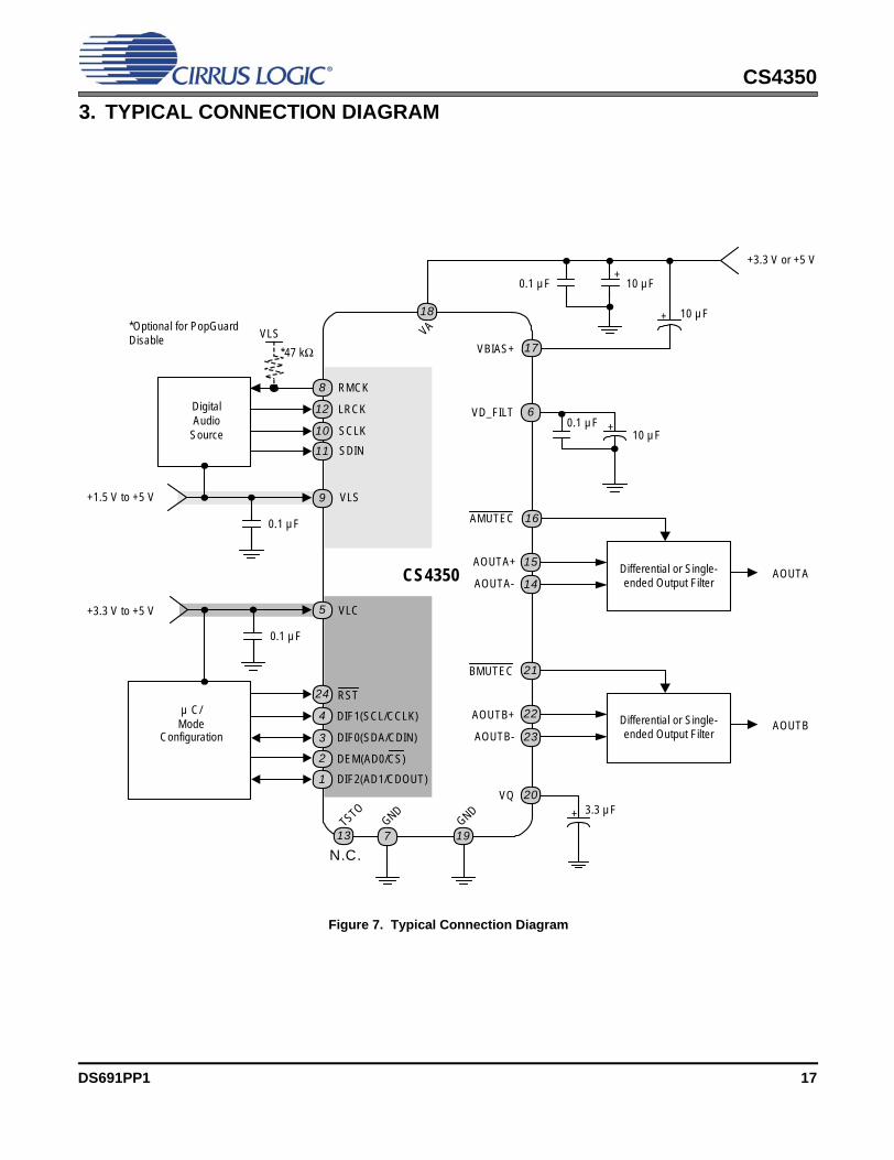
3. TYPICAL CONNECTION DIAGRAMDigitalAudio
Source
VLS
GND
CS4350
RMCK
AOUTA+
0.1 µF+
10 µF
µ C/Mode
Configuration
SDIN
DIF1(SCL/CCLK)
DIF0(SDA/CDIN)
3.3 µF
AOUTA
+
VBIAS+
VQ
LRCK
SCLK
AOUTB+
10 µF
VD_FILT
GND
0.1 µF
+1.5 V to +5 V
VA
0.1 µF10 µF
+3.3 V or +5 V
VLC
0.1 µF
+3.3 V to +5 V
VLS*Optional for PopGuard Disable
*47 kΩ
AOUTA-
AOUTB-
DIF2(AD1/CDOUT)
Differential or Single-ended Output Filter
AOUTB
TSTO
Differential or Single-ended Output Filter
+
+
8
12
10
11
9
5
24 RST4
3
2 DEM(AD0/CS)1
13 7 19
20
23
22
21BMUTEC
14
15
16AMUTEC
6
17
18
N.C.
Figure 7. Typical Connection Diagram
DS691PP1 17
CS4350
4. APPLICATIONS4.1 Sample Rate Range and Oversampling Mode DetectThe device operates in one of three oversampling modes based on the input sample rate. In Control PortMode, the allowed sample rate range in each mode will depend on how the FM[1:0] bits are configured. InStand-Alone Mode, the sample rate range will be according to Table 2.
4.1.1 Sample Rate Auto-Detect
The Auto-Detect feature is enabled by default. In this state, the CS4350 will auto-detect the correct modewhen the input sample rate (Fs), defined by the LRCK frequency, falls within one of the ranges shown inTable 2. Sample rates outside the specified range for each mode are not supported when Auto-Detect isenabled.
In Control Port Mode, the Auto-Detect feature can be disabled by the format bits in the control portregister 02h. In this state, the CS4350 will not auto-detect the correct mode based on the input samplerate (Fs). The operational mode must then be set manually according to one of the ranges referred to inSection 8.2.3. Sample rates outside the specified range for each mode are not supported. In Stand-AloneMode it is not possible to disable auto-detect of sample rates.
4.2 System ClockingThe device requires external generation of the left/right (LRCK) and serial (SCLK) clocks. The left/right clockfrequency is equal to the input sample rate (Fs).
Refer to Section 4.3 for the required SCLK-to-LRCK timing associated with the selected digital interface for-mat, and “Switching Specifications - Serial Audio Interface” on page 13 for the maximum allowed clock fre-quencies.
4.2.1 Recovered Master Clock (RMCK)
The CS4350 generates a high-frequency master clock (RMCK) which it derives from the LRCK input,available on the RMCK pin. In Stand-Alone Mode, the frequency of RMCK is equal to 256 x LRCK in Sin-gle-Speed and Double-Speed Mode; and 128 x LRCK in Quad-Speed Mode. In Control-Port Mode, thefrequency of the RMCK signal can be selected through register 08h (see Section 8.7 on page 34 for moredetails).
Input Sample Rate (Fs) Mode30 kHz - 54 kHz Single-Speed Mode60 kHz - 108 kHz Double-Speed Mode120 kHz - 216 kHz Quad-Speed Mode
Table 2. CS4350 Auto-Detect
18 DS691PP1

CS4350
4.3 Digital Interface FormatThe device will accept audio samples in 1 of 8 digital interface formats, as shown in Table 3 on page 24 forStand-Alone Mode and Table 4 on page 29 for Control Port Mode.
The desired serial audio interface format is selected via the DIF[2:0] bits in Control Port Mode (seeSection 8.2.1), or the DIF[2:0] pins in Stand-Alone Mode (see Section 5.1). For illustrations of the requiredrelationship between LRCK, SCLK and SDIN, see Figures 8-10. For all formats, SDIN is valid on the risingedge of SCLK.
For more information about serial audio formats, refer to the Cirrus Logic Application Note AN282, The 2-Channel Serial Audio Interface: A Tutorial, available at www.cirrus.com.
+3 +2 +1+5 +4MSB -1 -2 -3 -4 -5 +3 +2 +1+5 +4-1 -2 -3 -4LSB MSB LSB
Left Channel Right ChannelLRCK
SCLK
SDIN
Figure 8. Left-Justified up to 24-Bit Data
+3 +2 +1+5 +4MSB -1 -2 -3 -4 -5 +3 +2 +1+5 +4-1 -2 -3 -4MSBLSB LSB
Left Channel Right ChannelLRCK
SCLK
SDIN
Figure 9. I²S, up to 24-Bit Data
SDIN +6 +5 +4 +3 +2 +1+7-1 -2 -3 -4 -5LSB LSBMSB -1 -2 -3 -4 -5 LSB+6 +5 +4 +3 +2 +1+7MSB
Left Channel Right ChannelLRCK
SCLK
Figure 10. Right-Justified Data
DS691PP1 19

CS4350
4.3.1 Time-Division Multiplex (TDM) ModeFour TDM interface modes are available that allow the CS4350 to input stereo PCM data in one of 4 time“slots”. Figure 11 shows the serial port connections necessary to input 8-channel TDM data into fourCS4350 devices, and the corresponding DIF[2:0] pin or register-bit settings required for each CS4350.Figure 12 shows the TDM data format for each of the four CS4350 devices shown in Figure 11.
.
LRCK
SCLK
SDIN
ILRCK
ISCLK
SDIN
LRCK
SCLK
SDIN
LRCK SCLK TDM_OUT
TDM Source
CS43501 CS43502
LRCK
SCLK
SDIN
CS43503DIF[2:0] = 100 DIF[2:0] = 101 DIF[2:0] = 110 DIF[2:0] = 111
CS43504
Figure 11. TDM Mode Connection Diagram
Slot 2, ch B
LRCK
SCLK
MSB MSB MSB MSB MSBSDIN1
Slot 4, ch A Slot 4, ch BSlot 2, ch ASlot 1, ch A
256 clks
32 clks 32 clks 32 clks 32 clks 32 clks
MSB
Slot 3, ch A
32 clks
MSB
Slot 1, ch B
32 clks
MSB
Slot 3, ch B
32 clks
LSBMSB zeroData
Figure 12. TDM Mode Timing
20 DS691PP1

CS4350
4.4 De-EmphasisThe device includes on-chip digital de-emphasis. Figure 13 shows the de-emphasis curve for Fs equal to44.1 kHz. The frequency response of the de-emphasis curve will scale proportionally with changes in sam-ple rate, Fs.
Note: De-emphasis is only available in Single-Speed Mode.
4.5 Mute ControlThe mute control pins (AMUTEC and BMUTEC) go active during power-up initialization, reset, muting (seeSection 8.4.3), and loss of LRCK. These pins are intended to be used as control for external mute circuitsto prevent the clicks and pops that can occur in any single-ended single-supply system.
Use of the mute control function is not mandatory but recommended for designs requiring the absolute min-imum in extraneous clicks and pops. Also, use of the Mute Control function can enable the system designerto achieve idle-channel noise and signal-to-noise ratios which are only limited by the external mute circuit.
4.6 Recommended Power-Up Sequence
4.6.1 Stand-Alone Mode
1. Hold RST low until the power supplies and configuration pins are stable, and the master and left/right clocks are fixed to the appropriate frequencies, as discussed in Section 4.2. In this state, the control port registers are reset to their default settings, VQ will remain low, and VBIAS will be connected to VA.
2. Bring RST high. The device will remain in a low power state with VQ low for approximately 512 LRCK cycles in Single-Speed Mode (1024 LRCK cycles in Double-Speed Mode, and 2048 LRCK cycles in Quad-Speed Mode).
3. The device will then initiate the power up sequence which lasts approximately 50 µs when the Popguard is disabled. If the Popguard is enabled, see Section 4.7 for a complete description of power-up timing.
GaindB
-10dB
0dB
Frequency
T2 = 15 µs
T1=50 µs
F1 F23.183 kHz 10.61 kHz
Figure 13. De-Emphasis Curve
DS691PP1 21
CS4350
4.6.2 Control Port Mode1. Hold RST low until the power supply is stable and the left/right clock is fixed to the appropriate frequency, as discussed in Section 4.2. In this state, the control port is reset to its default settings, VQ will remain low, and VBIAS will be connected to VA.
2. Bring RST high. The device will remain in a low-power state with VQ low.
3. Perform a control port write to a valid register prior to the completion of approximately 512 LRCK cycles in Single-Speed Mode (1024 LRCK cycles in Double-Speed Mode, and 2048 LRCK cycles in Quad-Speed Mode). The desired register settings can be loaded while keeping the PDN bit set to 1.
4. Set the PDN bit to 0. This will initiate the power-up sequence, which lasts approximately 50 µs when the Popguard is disabled. If the Popguard is enabled, see Section 4.7 for a complete description of power-up timing.
4.7 Popguard Transient ControlThe CS4350 uses a novel technique to minimize the effects of output transients during power-up and power-down. This technology, when used with external DC-blocking capacitors in series with the audio outputs,minimizes the audio transients commonly produced by single-ended single-supply converters. It is activatedinside the DAC when the RST pin is toggled and requires no other external control, aside from choosing theappropriate DC-blocking capacitors.
4.7.1 Power-UpWhen the device is initially powered-up, the audio outputs, AOUTA and AOUTB, are clamped to GND.Following a delay of approximately 1000 sample periods, each output begins to ramp toward the quies-cent voltage. Approximately 10,000 LRCK cycles later, the outputs reach VQ and audio output begins.This gradual voltage ramping allows time for the external DC-blocking capacitors to charge to the quies-cent voltage, minimizing audible power-up transients.
4.7.2 Power-DownTo prevent audible transients at power-down, the device must first enter its power-down state. When thisoccurs, audio output ceases and the internal output buffers are disconnected from AOUTA and AOUTB.In their place, a soft-start current sink is substituted which allows the DC-blocking capacitors to slowly dis-charge. Once this charge is dissipated, the power to the device may be turned off, and the system is readyfor the next power-on.
4.7.3 Discharge Time
To prevent an audio transient at the next power-on, the DC-blocking capacitors must fully discharge be-fore turning on the power or exiting the power-down state. If full discharge does not occur, a transient willoccur when the audio outputs are initially clamped to GND. The time that the device must remain in thepower-down state is related to the value of the DC-blocking capacitance and the output load. For example,with a 3.3 µF capacitor, the minimum power-down time will be approximately 0.4 seconds.
22 DS691PP1

CS4350
4.8 Analog Output and FilteringThe Cirrus Application Note titled Design Notes for a 2-Pole Filter with Differential Input, available as AN48at www.cirrus.com, discusses the second-order Butterworth filter and differential-to-single-ended converterthat was implemented on the CS4350 evaluation board, CDB4350. Figure 14 illustrates thisimplementation. If only single-ended outputs from the CS4350 are required, the passive output filter shownin Figure 15 can be used.
4.9 Grounding and Power Supply ArrangementsAs with any high-resolution converter, the CS4350 requires careful attention to power supply and groundingarrangements if its potential performance is to be realized. Figure 7 shows the recommended power ar-rangements, with VA, VLC, and VLS connected to clean supplies. The use of split analog and digital groundplanes is not recommended. However, if planes are split between digital ground and analog ground theGND pins of the CS4350 should be connected to the analog ground plane.
All signals, especially clocks, should be kept away from the VBIAS, VFILT, and VQ pins in order to avoidunwanted coupling into the DAC.
4.9.1 Capacitor Placement
Decoupling capacitors should be placed as close to the DAC as possible, with the low value ceramic ca-pacitor being the closest. To further minimize impedance, these capacitors should be located on the samelayer as the DAC. If desired, all supply pins may be connected to the same supply, but a decoupling ca-pacitor should still be placed on each supply pin.
Note: All decoupling capacitors should be referenced to analog ground.
The CDB4350 evaluation board demonstrates the optimum layout and power supply arrangements.
AOUTx +
AOUTx - -
+
1000 pF
C0G562 Ω22 μF
4.02 kΩ5600 pF
C0G
221 Ω
392 Ω4.64 kΩ
1.62 kΩ
1.37 kΩ 22 μF
2700 pF
C0G.015 μF
C0G
47 kΩ
CS4350
AGND
Analog Output
Figure 14. Differential to Single-Ended Output Filter
AOUTx +3.3 µF
Analog Output
2200 pF
+
10 kΩ
CS4350
AGND
560 Ω
Figure 15. Passive Single-Ended Output Filter
DS691PP1 23

CS4350
5. STAND-ALONE OPERATION5.1 Serial Port Format SelectionThe desired serial audio format is selected with the DIF2, DIF1 and DIF0 pins. For an explanation of therequired relationship between the LRCK, SCLK and SDIN, see Figures 8-10. For all formats, SDIN is validon the rising edge of SCLK. TDM Mode requires the selection of which stereo pair time “slot” is used to out-put data as shown in Table 3 and Figure 12.
5.2 De-Emphasis ControlWhen pulled to VLC, the DEM pin activates the 44.1 kHz de-emphasis filter. When pulled to GND, the DEMpin turns off the de-emphasis filter.
5.3 Popguard Transient ControlIn Stand-Alone Mode, Popguard is enabled by default. Popguard can be defeated in Stand-Alone Mode byplacing a 47 kΩ resistor between RMCK and VLS.
DIF2 DIF1 DIF0 DESCRIPTION FORMAT FIGURE0 0 0 Left-Justified, up to 24-bit data 0 90 0 1 I²S, up to 24-bit data 1 80 1 0 Right-Justified, 16-bit data 2 100 1 1 Right-Justified, 24-bit data 3 101 0 0 TDM slot 0 4 121 0 1 TDM slot 1 5 121 1 0 TDM slot 2 6 121 1 1 TDM slot 3 7 12
Table 3. Digital Interface Format - Stand-Alone Mode
24 DS691PP1

CS4350
6. CONTROL PORT OPERATIONThe control port is used to load all the internal register settings (see ”Register Description” on page 29). The oper-ation of the control port may be completely asynchronous with the audio sample rate. However, to avoid potentialinterference problems, the control port pins should remain static if no operation is required.The control port can operate in I²C or SPI mode.
6.1 MAP Auto IncrementThe device has a MAP (memory address pointer) auto-increment capability enabled by the INCR bit (alsothe MSB) of the MAP. If INCR is set to 0, MAP will stay constant for consecutive writes or reads. If INCR isset to 1, MAP will auto increment after each byte is read or written, allowing block reads or writes of con-secutive registers.
6.2 I²C ModeIn the I²C Mode, data is clocked into and out of the bi-directional serial control data line, SDA, by the serialcontrol port clock, SCL (see Figure 16 for the clock to data relationship). There is no CS pin. AD1 and AD0enable the user to alter the chip address (10010[AD1][AD0][R/W]) and should be tied to VLC or GND asrequired before powering up the device. SPI Mode will be selected if the device ever detects a high to lowtransition on the AD0/CS pin after power-up.
6.2.1 I²C Write
To write to the device, follow the procedure below while adhering to the control port Switching Specifica-tions in ”Switching Characteristics - Control Port - I²C Format” on page 14.
1. Initiate a START condition to the I²C bus followed by the address byte. The upper 5 bits must be 10010. The sixth and seventh bit must match the settings of the AD1 and AD0 pins respectively, and the eighth must be 0 (the eighth bit of the address byte is the R/W bit).
2. Wait for an acknowledge (ACK) from the part, then write to the memory address pointer, MAP. This byte points to the register to be written.
3. Wait for an acknowledge (ACK) from the part, then write the desired data to the register pointed to by the MAP.
4. If the INCR bit (see Section 6.1) is set to 1, repeat the previous step until all the desired registers are written, then initiate a STOP condition to the bus.
5. If the INCR bit is set to 0 and further I²C writes to other registers are desired, it is necessary to initiate a repeated START condition and follow the procedure detailed from step 1. If no further writes to other registers are desired, initiate a STOP condition to the bus.
6.2.2 I²C Read
To read from the device, follow the procedure below while adhering to the control port switching specifi-cations in ”Switching Characteristics - Control Port - I²C Format” on page 14.
1. Initiate a START condition to the I²C bus followed by the address byte. The upper 5 bits must be 10010. The sixth and seventh bits must match the setting of the AD1 and AD0 pins, respectively, and the eighth must be 1. The eighth bit of the address byte is the R/W bit.
2. After transmitting an acknowledge (ACK), the device will then transmit the contents of the register pointed to by the MAP. The MAP register will contain the address of the last register written to the
DS691PP1 25

CS4350
MAP or the default address (see Section 6.4.2) if an I²C read is the first operation performed on the device.3. Once the device has transmitted the contents of the register pointed to by the MAP, issue an ACK.
4. If the INCR bit is set to 1, the device will continue to transmit the contents of successive registers. Continue providing a clock and issue an ACK after each byte until all the desired registers are read; then initiate a STOP condition to the bus.
5. If the INCR bit is set to 0 and further I²C reads from other registers are desired, it is necessary to initiate a repeated START condition and follow the procedure detailed from steps 1 and 2 from the I²C Write instructions, followed by step 1 of the I²C Read section. If no further reads from other registers are desired, initiate a STOP condition to the bus.
6.3 SPI ModeIn SPI Mode, data is clocked into the serial control data line, CDIN, by the serial control port clock, CCLK(see Figure 17 for the clock to data relationship). There are no AD0 or AD1 pins. Pin CS is the chip selectsignal and is used to control SPI writes to the control port. When the device detects a high-to-low transitionon the AD0/CS pin after power-up, SPI Mode will be selected. All signals are inputs and data is clocked inon the rising edge of CCLK.
6.3.1 SPI WriteTo write to the device, follow the procedure below while adhering to the control port switching specifica-tions in ”Switching Characteristics - Control Port - SPI Format” on page 15.
1. Bring CS low.
2. The address byte on the CDIN pin must then be 10011110 (R/W = 0).
3. Write to the memory address pointer, MAP. This byte points to the register to be written.
4. Write the desired data to the register pointed to by the MAP.
5. If the INCR bit (see Section 6.1) is set to 1, repeat the previous step until all the desired registers are written, then bring CS high.
6. If the INCR bit is set to 0 and further SPI writes to other registers are desired, it is necessary to bring CS high, and follow the procedure detailed from step 1. If no further writes to other registers are desired, bring CS high
4 5 6 7 24 25
SCL
CHIP ADDRESS MAP BYTE DATA DATA +1
START
ACK
STOP
ACKACKACK
1 0 0 1 0 AD1 AD0 R/WSDA 6 5 4 3 2 1 0 7 6 1 0 7 6 1 0 7 6 1 0
0 1 2 3 8 9 12 16 17 18 19 10 11 13 14 15 27 2826
DATA +n
INC
Figure 16. Control Port Timing, I²C Mode
26 DS691PP1

CS4350
6.3.2 SPI ReadTo read from the device, follow the procedure below while adhering to the values specified in ”SwitchingCharacteristics - Control Port - SPI Format” on page 15.
1. Bring CS low.
2. The address byte on the CDIN pin must then be 10011111 (R/W = 1).
3. CDOUT pin will then output the data from the register pointed to by the MAP, which is set during the SPI write operation.
4. If the INCR bit (see Section 6.1) is set to 1, keep CS low and continue providing clocks on CCLK to read from multiple consecutive registers. Bring CS high when reading is complete.
5. If the INCR bit is set to 0 and further SPI reads from other registers are desired, it is necessary to bring CS high, and follow the procedure detailed from step 1. If no further reads from other registers are desired, bring CS high.
6.4 Memory Address Pointer (MAP)
6.4.1 INCR (Auto Map Increment Enable)
Default = ‘0’0 - Disabled1 - Enabled
6.4.2 MAP (Memory Address Pointer)
Default = ‘0000’
7 6 5 4 3 2 1 0INCR Reserved Reserved Reserved MAP3 MAP2 MAP1 MAP0
0 0 0 0 0 0 0 0
M A P
MSB LSB
DATA
b y te 1 b y te n
R/W R/W
A D D R E S SC H IP
ADDRESSC H IP
MSB LSB MSB LSB
MAP = Memory Address Pointer, 8 bits, MSB first
High Impedance
1001111 1001111
CCLK
CDIN
CDOUT
CS
Figure 17. Control Port Timing, SPI Mode
DS691PP1 27

CS4350
7. REGISTER QUICK REFERENCEAddr Function 7 6 5 4 3 2 1 01h Device and RevID DeviceID4 DeviceID3 DeviceID2 DeviceID1 DeviceID0 RevID2 RevID1 RevID0default 1 1 1 1 - - - -
2h Mode Control Reserved DIF2 DIF1 DIF0 DEM1 DEM0 FM1 FM0default 0 0 0 0 0 0 0 0
3h Volume, Mixing, and Inversion Control
VOLB=A INVERTA INVERTB Reserved ATAPI3 ATAPI2 ATAPI1 ATAPI0
default 0 0 0 0 1 0 0 14h Mute Control AMUTE Reserved MUTEC
A=BMUTE_A MUTE_B Reserved Reserved Reserved
default 1 0 0 0 0 0 0 15h Channel A Volume
ControlVOL7 VOL6 VOL5 VOL4 VOL3 VOL2 VOL1 VOL0
default 0 0 0 0 0 0 0 06h Channel B Volume
ControlVOL7 VOL6 VOL5 VOL4 VOL3 VOL2 VOL1 VOL0
default 0 0 0 0 0 0 0 07h Ramp and Filter
ControlSZC1 SZC0 RMP_UP RMP_DN Reserved FILT_SEL Reserved Reserved
default 1 0 1 1 0 0 0 18h Misc. Control PDN Reserved FREEZE POPG_EN RMCK_
CTRL1RMCK_CTRL0
R_SELECT1
R_SELECT0
default 0 0 0 1 0 0 0 0
28 DS691PP1

CS4350
8. REGISTER DESCRIPTION** All register access is R/W unless specified otherwise**8.1 Device and Revision ID - Register 01h
Function:
This register is Read-Only. It is decoded as follows:
8.2 Mode Control - Register 02h
8.2.1 Digital Interface Format (DIF[2:0]) Bits 6-4Function:
These bits select the interface format for the serial audio input.
The required relationship between the Left/Right clock, serial clock and serial data is defined by the DigitalInterface Format and the options are detailed in Figures 8-10.
7 6 5 4 3 2 1 0Device4 Device3 Device2 Device1 Device0 Rev2 Rev1 Rev0
1 1 1 1 - - - -
Rev Register 01h contentsA 1111,0000B 1111,0001
C2 1111,1111
7 6 5 4 3 2 1 0Reserved DIF2 DIF1 DIF0 DEM1 DEM0 FM1 FM0
0 0 0 0 0 0 0 0
DIF2 DIF1 DIF0 Description Format Figure0 0 0 Left-Justified, up to 24-bit data 0 (Default) 80 0 1 I²S, up to 24-bit data 1 90 1 0 Right-Justified, 16-bit data 2 100 1 1 Right-Justified, 24-bit data 3 101 0 0 TDM slot 0 4 121 0 1 TDM slot 1 5 121 1 0 TDM slot 2 6 121 1 1 TDM slot 3 7 12
Table 4. Digital Interface Formats
DS691PP1 29

CS4350
8.2.2 De-Emphasis Control (DEM[1:0]) Bits 3-2Default = 000 - No De-emphasis01 - 44.1 kHz De-emphasis10 - 48 kHz De-emphasis11 - 32 kHz De-emphasis
Function:
Selects the appropriate digital filter to maintain the standard15 μs/50 μs digital de-emphasis filter response at 32, 44.1or 48 kHz sample rates. (See Figure 18) Note: De-emphasis is only available in Single-SpeedMode
8.2.3 Functional Mode (FM[1:0]) Bits 1-0
Default = 0000 - Auto speed mode detect01 - Single-Speed Mode (30 to 54 kHz sample rates)10 - Double-Speed Mode (50 to 108 kHz sample rates)11 - Quad-Speed Mode (100 to 216 kHz sample rates)
Function:
Selects the required range of input sample rates or auto speed mode.
8.3 Volume Mixing and Inversion Control - Register 03h
8.3.1 Channel A Volume = Channel B Volume (VOLB=A) Bit 7
Function:
When set to 0 (default), the AOUTA and AOUTB volume levels are independently controlled by the A andthe B Channel Volume Control Bytes.
When set to 1, the volume on both AOUTA and AOUTB are determined by the A Channel Attenuation andVolume Control Bytes, and the B Channel Bytes are ignored.
8.3.2 Invert Signal Polarity (INVERT_A) Bit 6
Function:
When set to 1, this bit inverts the signal polarity of channel A.
When set to 0 (default), this function is disabled.
This function is only available for Left Justified, Right Justified 16, and Right Justified 24 data formats.
7 6 5 4 3 2 1 0VOLB=A INVERT_A INVERT_B Reserved ATAPI3 ATAPI2 ATAPI1 ATAPI0
0 0 0 0 1 0 0 1
GaindB
-10dB
0dB
Frequency
T2 = 15 µs
T1=50 µs
F1 F23.183 kHz 10.61 kHz
Figure 18. De-Emphasis Curve
30 DS691PP1

CS4350
8.3.3 Invert Signal Polarity (INVERT_B) Bit 5Function:
When set to 1, this bit inverts the signal polarity of channel B.
When set to 0 (default), this function is disabled.
This function is only available for Left Justified, Right Justified 16, and Right Justified 24 data formats.
8.3.4 ATAPI Channel Mixing and Muting (ATAPI[3:0]) Bits 3-0
Default = 1001 - AOUTA=aL, AOUTB=bR (Stereo)
Function:
The CS4350 implements the channel mixing functions of the ATAPI CD-ROM specification. Refer toTable 5 and Figure 19 for additional information.
ATAPI_A1 ATAPI_A0 ATAPI_B1 ATAPI_B0 AOUTA AOUTB0 0 0 0 MUTE MUTE0 0 0 1 MUTE bR0 0 1 0 MUTE bL0 0 1 1 MUTE b[(L+R)/2]0 1 0 0 aR MUTE0 1 0 1 aR bR0 1 1 0 aR bL0 1 1 1 aR b[(L+R)/2]
Table 5. ATAPI Decode
Σ Σ
A ChannelVolume Control
AoutA
AoutB
Left ChannelAudio Data
Right ChannelAudio Data
B ChannelVolume Control
MUTE
MUTE
Figure 19. ATAPI Block Diagram
DS691PP1 31

CS4350
8.4 Mute Control - Register 04h
8.4.1 Auto-Mute (AMUTE) Bit 7
Function:
When set to 1 (default), the Digital-to-Analog converter output will mute following the reception of 8192consecutive audio samples of static 0 or -1. A single sample of non-static data will release the mute. De-tection and muting is done independently for each channel. The quiescent voltage on the output will beretained and the Mute Control pin will go active during the mute period.
When set to 0, this function is disabled
8.4.2 AMUTEC = BMUTEC (MUTEC A=B) Bit 5Function:
When set to 0 (default) the AMUTEC and BMUTEC pins operate independently.
When set to 1, the individual controls for AMUTEC and BMUTEC are internally connected through anAND gate prior to the output pins. Therefore, the external AMUTEC and BMUTEC pins will go active onlywhen the requirements for both AMUTEC and BMUTEC are valid.
8.4.3 Channel A Mute (MUTE_A) Bit 4 & Channel B Mute (MUTE_B) Bit 3
Function:
When set to 1, the Digital-to-Analog converter output will mute. The quiescent voltage on the output willbe retained. The muting function is effected, similar to attenuation changes, by the Soft and Zero Crossbits in the Volume and Mixing Control register. The corresponding MUTEC pin will go active following anyramping due to the soft and zero cross function.
When set to 0 (default), this function is disabled.
1 0 0 0 aL MUTE1 0 0 1 aL bR1 0 1 0 aL bL1 0 1 1 aL b[(L+R)/2]1 1 0 0 a[(L+R)/2] MUTE1 1 0 1 a[(L+R)/2] bR1 1 1 0 a[(L+R)/2] bL1 1 1 1 a[(L+R)/2] b[(L+R)/2]
7 6 5 4 3 2 1 0AMUTE Reserved MUTEC A=B MUTE_A MUTE_B Reserved Reserved Reserved
1 0 0 0 0 0 0 0
ATAPI_A1 ATAPI_A0 ATAPI_B1 ATAPI_B0 AOUTA AOUTB
Table 5. ATAPI Decode
32 DS691PP1

CS4350
8.5 Channel A & B Volume Control - Register 05h & 06hDigital Volume Control (VOL[7:0]) Bits 7-0
Default = 00h (0 dB)
Function:
The Digital Volume Control registers allow independent control of the signal levels in 1/2 dB incrementsfrom 0 to -127.5 dB. Volume settings are decoded as shown in Table 6. The volume changes are imple-mented as dictated by the Soft and Zero Cross bits in the Power and Muting Control register. The actualattenuation is determined by taking the decimal value of the volume register and multiplying by 6.02/12.
8.6 Ramp and Filter Control - Register 07h
8.6.1 Soft Ramp and Zero Cross Control (SZC[1:0]) Bits 7-6Default = 10
Function:
Immediate Change
When Immediate Change is selected all level changes will take effect immediately in one step.
Zero Cross
Zero Cross Enable dictates that signal level changes, either by attenuation changes or muting, will occuron a signal zero crossing to minimize audible artifacts. The requested level change will occur after a time-out period between 512 and 1024 sample periods (10.7 ms to 21.3 ms at 48 kHz sample rate) if the signaldoes not encounter a zero crossing. The zero cross function is independently monitored and implementedfor each channel.
Soft Ramp PCM
Soft Ramp allows level changes, both muting and attenuation, to be implemented by incrementally ramp-ing, in 1/8 dB steps, from the current level to the new level at a rate of 1 dB per 8 left/right clock periods.
7 6 5 4 3 2 1 0VOL7 VOL6 VOL5 VOL4 VOL3 VOL2 VOL1 VOL0
0 0 0 0 0 0 0 0
Binary Code Decimal Value Volume Setting00000000 0 0 dB00000001 1 -0.5 dB00000110 6 -3.0 dB11111111 255 -127.5 dB
Table 6. Example Digital Volume Settings
7 6 5 4 3 2 1 0SZC1 SZC0 RMP_UP RMP_DN Reserved FILT_SEL Reserved Reserved
1 0 1 1 0 0 0 1
SZC1 SZC0 Description0 0 Immediate Change0 1 Zero Cross1 0 Soft Ramp1 1 Soft Ramp on Zero Crossings
DS691PP1 33

CS4350
Soft Ramp and Zero CrossSoft Ramp and Zero Cross Enable dictate that signal level changes, either by attenuation changes or mut-ing, will occur in 1/8 dB steps and be implemented on a signal zero crossing. The 1/8 dB level change willoccur after a time-out period between 512 and 1024 sample periods (10.7 ms to 21.3 ms at 48 kHz samplerate) if the signal does not encounter a zero crossing. The zero cross function is independently monitoredand implemented for each channel.
8.6.2 Soft Volume Ramp-Up after Error (RMP_UP) Bit 5
Function:
When set to 1 (default), an un-mute will be performed after executing a filter mode change, after LRCK islost, and after changing the Functional Mode. This un-mute is affected, similar to attenuation changes, bythe Soft and Zero Cross bits in the Volume and Mixing Control register.
When set to 0, an immediate un-mute is performed in these instances.
Note: For best results, it is recommended that this feature be used in conjunction with the RMP_DN bit.
8.6.3 Soft Ramp-Down before Filter Mode Change (RMP_DN) Bit 4
Function:
When set to 1 (default), a mute will be performed prior to executing a filter mode change. This mute isaffected, similar to attenuation changes, by the Soft and Zero Cross bits in the Volume and Mixing Controlregister.
When set to 0, an immediate mute is performed prior to executing a filter mode change.
Note: For best results, it is recommended that this feature be used in conjunction with the RMP_UP bit.
8.6.4 Interpolation Filter Select (FILT_SEL) Bit 2
Function:
When set to 0 (default), the Interpolation Filter has a fast roll off.
When set to 1, the Interpolation Filter has a slow roll off.
The specifications for each filter can be found in the ”Combined Interpolation & On-Chip Analog Filter Re-sponse” on page 12, and response plots can be found in Figures 22 through 27.
8.7 Misc. Control - Register 08h
8.7.1 Power Down (PDN) Bit 7Function:
When set to 1 the entire device will enter a low-power state and the contents of the control registers willbe retained. The power-down bit defaults to ‘0’ on power-up.
7 6 5 4 3 2 1 0PDN Reserved FREEZE POPG_EN RMCK_CTRL1 RMCK_CTRL0 R_SELECT1 R_SELECT0
0 0 0 1 0 0 0 0
34 DS691PP1

CS4350
8.7.2 Freeze Controls (FREEZE) Bit 5Function:
When set to 1, this function allows modifications to be made to the registers without the changes takingeffect until FREEZE is set back to 0. To make multiple changes in the Control Port registers take effectsimultaneously, enable the FREEZE bit, make all register changes, then disable the FREEZE bit.
When set to 0 (default), register changes take effect immediately.
8.7.3 Popguard Enable (POPG_EN) Bit 4
Function:
When set to 1, (default) the Device will initiate a ramping function as outlined in Section 4.7 on page 22.When set to 0, the outputs will step to VQ upon release of PDN.
8.7.4 RMCK control (RMCK_CTR[1:0]) Bits 3:2
Default = 00
Function: These bits set the function of the RMCK pin with respect to the LRCK.
8.7.5 RMCK Ratio Select (R_SELECT[1:0]) Bits 2:1
Default = 00
Function: To select the RMCK-to-LRCK ratio.
Note: RMCK_CTR must be set to 10 to enable this function. Please note the maximum RMCK outputfrequency as specified in the ”Switching Specifications - Serial Audio Interface” on page 13.
RMCK_CTR1 RMCK_CTR0 Mode0 0 256x LRCK for 48 kHz and 96 kHz, 128x @ 192kHz 0 1 512x @ 48kHz, 256x @ 96 kHz, 128x @ 192kHz 1 0 Manual control (see RMCK_RATIO)1 1 RMCK off
R_SELECT1 R_SELECT0 RMCK/LRCK Ratio0 0 5120 1 2561 0 1281 1 64
DS691PP1 35

CS4350
9. FILTER PLOTS0.4 0.5 0.6 0.7 0.8 0.9 1120
100
80
60
40
20
0
Frequency(normalized to Fs)
Am
plit
ud
e (d
B)
Figure 20. Stopband Rejection (fast), all Modes Figure 21. Stopband Rejection (slow), all Modes
0.4 0.5 0.6 0.7 0.8 0.9 1120
100
80
60
40
20
0
Frequency(normalized to Fs)
Am
plit
ud
e (d
B)
Figure 22. Single-Speed (fast) Passband Detail Figure 23. Single-Speed (slow) Passband Detail
0 0.05 0.1 0.15 0.2 0.25 0.3 0.35 0.4 0.45 0.50.02
0.015
0.01
0.005
0
0.005
0.01
0.015
0.02
Frequency(normalized to Fs)
Am
plit
ud
e (d
B)
0 0.05 0.1 0.15 0.2 0.25 0.3 0.35 0.4 0.45 0.50.02
0.015
0.01
0.005
0
0.005
0.01
0.015
0.02
Frequency(normalized to Fs)
Am
plit
ud
e (d
B)
0 0.05 0.1 0.15 0.2 0.25 0.3 0.35 0.4 0.45 0.5−0.5
−0.4
−0.3
−0.2
−0.1
0
0.1
0.2
0.3
0.4
0.5
Frequency (normalized to Fs)
Am
plitu
de (
dB)
0 0.05 0.1 0.15 0.2 0.25 0.3 0.35 0.4 0.45 0.5−0.5
−0.4
−0.3
−0.2
−0.1
0
0.1
0.2
0.3
0.4
0.5
Frequency (normalized to Fs)
Am
plitu
de (
dB)
Figure 24. Double-Speed (fast) Passband Detail Figure 25. Double-Speed (slow) Passband Detail
36 DS691PP1

CS4350
0 0.05 0.1 0.15 0.2 0.25 0.3−0.5
−0.4
−0.3
−0.2
−0.1
0
0.1
0.2
0.3
0.4
0.5
Frequency (normalized to Fs)
Am
plitu
de (
dB)
0 0.05 0.1 0.15 0.2 0.25 0.3−0.5
−0.4
−0.3
−0.2
−0.1
0
0.1
0.2
0.3
0.4
0.5
Frequency (normalized to Fs)
Am
plitu
de (
dB)
Figure 26. Quad-Speed (fast) Passband Detail Figure 27. Quad-Speed (slow) Passband Detail
DS691PP1 37

CS4350
10.PARAMETER DEFINITIONSTotal Harmonic Distortion + Noise (THD+N)The ratio of the rms value of the signal to the rms sum of all other spectral components over the specifiedbandwidth (typically 10 Hz to 20 kHz), including distortion components. Expressed in decibels.
Dynamic Range
The ratio of the full-scale rms value of the signal to the rms sum of all other spectral components over thespecified bandwidth. Dynamic range is a signal-to-noise measurement over the specified bandwidth madewith a -60 dBFS signal. Then, 60 dB is added to the resulting measurement to refer the measurement to fullscale. This technique ensures that the distortion components are below the noise level and do not effect themeasurement. This measurement technique has been accepted by the Audio Engineering Society, AES17-1991, and the Electronic Industries Association of Japan, EIAJ CP-307.
Interchannel Isolation
A measure of crosstalk between the left and right channels. Measured for each channel at the converter'soutput with all zeros to the input under test and a full-scale signal applied to the other channel. Units in deci-bels.
Interchannel Gain Mismatch
The gain difference between left and right channels. Units in decibels.
Gain Error
The deviation from the nominal full-scale analog output for a full-scale digital input.
Gain Drift
The change in gain value with temperature. Units in ppm/°C.
Intra-Channel Phase Deviation
The deviation from linear phase within a given channel.
Inter-Channel Phase Deviation
The difference in phase between channels.
38 DS691PP1

CS4350
11.PACKAGE DIMENSIONS1. D” and “E1” are reference datums and do not included mold flash or protrusions, but do include moldmismatch and are measured at the parting line, mold flash or protrusions shall not exceed 0.20 mm perside.
2. Dimension “b” does not include dambar protrusion/intrusion. Allowable dambar protrusion shall be 0.13 mm total inexcess of “b” dimension at maximum material condition. Dambar intrusion shall not reduce dimension “b” by morethan 0.07 mm at least material condition.
3. These dimensions apply to the flat section of the lead between 0.10 and 0.25 mm from lead tips.
THERMAL CHARACTERISTICS
INCHES MILLIMETERS NOTEDIM MIN NOM MAX MIN NOM MAX
A -- -- 0.043 -- -- 1.10A1 0.002 0.004 0.006 0.05 -- 0.15A2 0.03346 0.0354 0.037 0.85 0.90 0.95b 0.00748 0.0096 0.012 0.19 0.245 0.30 2,3D 0.303 0.307 0.311 7.70 7.80 7.90 1E 0.248 0.2519 0.256 6.30 6.40 6.50E1 0.169 0.1732 0.177 4.30 4.40 4.50 1e -- 0.026 BSC -- -- 0.65 BSC --L 0.020 0.024 0.028 0.50 0.60 0.70µ 0° 4° 8° 0° 4° 8°
JEDEC #: MO-153Controlling Dimension is Millimeters.
Parameters Symbol Min Typ Max UnitsPackage Thermal Resistance Single-Layer PCB
Multi-Layer PCB θJA - 70105 - °C/Watt
24L TSSOP (4.4 mm BODY) PACKAGE DRAWING
E
N
1 2 3
e b2 A1
A2 A
D
SEATINGPLANE
E11
L
SIDE VIEW
END VIEW
TOP VIEW
∝
DS691PP1 39

CS4350
12.ORDERING INFORMATION13.REVISION HISTORY
Product Description Package Pb-Free Grade Temp Range Container Order#
CS4350 192 kHz Stereo DAC with Integrated PLL 24-TSSOP YES
Commercial -40° to +85°CRail CS4350-CZZ
Tape and Reel CS4350-CZZR
Automotive -40° to +105°CRail CS4350-DZZ
Tape and Reel CS4350-DZZRCDB4350 Evaluation Board for CS4350 - - - - CDB4350
Release Changes
A2
-Changed description of TSTO pin in “Pin Description” on page 7 and “Typical Connection Dia-gram” on page 17.-Corrected Full-Scale Voltage in “RL and CL represent the minimum resistance and maximum capacitance required for the CS4350’s internal op-amp to remain stable. See Figure 1 and Figure 2 for more details.” on page 9-Changed base address in “I²C Mode” on page 25 and “SPI Mode” on page 26.
A3 Corrected typographical error in chip address shown in Section 6.2 on page 25.Corrected typographical error in value stated for the upper five bits in Section 6.2.1 on page 25.
PP1
-Updated “DAC Analog Characteristics - Commercial (-CZZ)” on page 9-Added “DAC Analog Characteristics - Automotive (-DZZ)” on page 10-Updated “Switching Specifications - Serial Audio Interface” on page 13-Updated “Power and Thermal Characteristics” on page 16
Contacting Cirrus Logic SupportFor all product questions and inquiries, contact a Cirrus Logic Sales Representative. To find the one nearest you, go to www.cirrus.com.
IMPORTANT NOTICE"Preliminary" product information describes products that are in production, but for which full characterization data is not yet available. Cirrus Logic, Inc. and its sub-sidiaries ("Cirrus") believe that the information contained in this document is accurate and reliable. However, the information is subject to change without notice andis provided "AS IS" without warranty of any kind (express or implied). Customers are advised to obtain the latest version of relevant information to verify, beforeplacing orders, that information being relied on is current and complete. All products are sold subject to the terms and conditions of sale supplied at the time of orderacknowledgment, including those pertaining to warranty, indemnification, and limitation of liability. No responsibility is assumed by Cirrus for the use of this informa-tion, including use of this information as the basis for manufacture or sale of any items, or for infringement of patents or other rights of third parties. This documentis the property of Cirrus and by furnishing this information, Cirrus grants no license, express or implied under any patents, mask work rights, copyrights, trademarks,trade secrets or other intellectual property rights. Cirrus owns the copyrights associated with the information contained herein and gives consent for copies to bemade of the information only for use within your organization with respect to Cirrus integrated circuits or other products of Cirrus. This consent does not extend toother copying such as copying for general distribution, advertising or promotional purposes, or for creating any work for resale. CERTAIN APPLICATIONS USING SEMICONDUCTOR PRODUCTS MAY INVOLVE POTENTIAL RISKS OF DEATH, PERSONAL INJURY, OR SEVERE PROP-ERTY OR ENVIRONMENTAL DAMAGE (“CRITICAL APPLICATIONS”). CIRRUS PRODUCTS ARE NOT DESIGNED, AUTHORIZED OR WARRANTED FOR USEIN AIRCRAFT SYSTEMS, MILITARY APPLICATIONS, PRODUCTS SURGICALLY IMPLANTED INTO THE BODY, AUTOMOTIVE SAFETY OR SECURITY DE-VICES, LIFE SUPPORT PRODUCTS OR OTHER CRITICAL APPLICATIONS. INCLUSION OF CIRRUS PRODUCTS IN SUCH APPLICATIONS IS UNDERSTOODTO BE FULLY AT THE CUSTOMER’S RISK AND CIRRUS DISCLAIMS AND MAKES NO WARRANTY, EXPRESS, STATUTORY OR IMPLIED, INCLUDING THEIMPLIED WARRANTIES OF MERCHANTABILITY AND FITNESS FOR PARTICULAR PURPOSE, WITH REGARD TO ANY CIRRUS PRODUCT THAT IS USEDIN SUCH A MANNER. IF THE CUSTOMER OR CUSTOMER’S CUSTOMER USES OR PERMITS THE USE OF CIRRUS PRODUCTS IN CRITICAL APPLICA-TIONS, CUSTOMER AGREES, BY SUCH USE, TO FULLY INDEMNIFY CIRRUS, ITS OFFICERS, DIRECTORS, EMPLOYEES, DISTRIBUTORS AND OTHERAGENTS FROM ANY AND ALL LIABILITY, INCLUDING ATTORNEYS’ FEES AND COSTS, THAT MAY RESULT FROM OR ARISE IN CONNECTION WITHTHESE USES.Cirrus Logic, Cirrus, the Cirrus Logic logo designs, and Popguard are trademarks of Cirrus Logic, Inc. All other brand and product names in this document may betrademarks or service marks of their respective owners.
I²C is a registered trademark of Philips SemiconductorSPI is a trademark of Motorola, Inc.
40 DS691PP1