cse-45432 introduction to computer architecture chapter …bai/cse45432/comp_arch_chp5_3rd.pdf ·...
TRANSCRIPT

1
CSE-45432 Introduction to Computer
Architecture
Chapter 5 The Processor:
Datapath & Control
Dr. Izadi
ECE 45432 SUNY New Paltz2
RegistersRegister #
Data
Register #
Data�memory
Address
Data
Register #
PC Instruction ALU
Instruction�memory
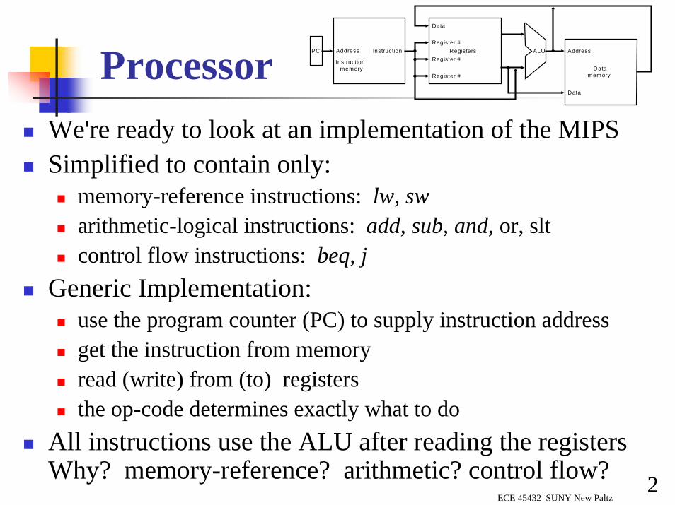
AddressProcessorWe're ready to look at an implementation of the MIPSSimplified to contain only:
memory-reference instructions: lw, swarithmetic-logical instructions: add, sub, and, or, sltcontrol flow instructions: beq, j
Generic Implementation:use the program counter (PC) to supply instruction addressget the instruction from memoryread (write) from (to) registersthe op-code determines exactly what to do
All instructions use the ALU after reading the registersWhy? memory-reference? arithmetic? control flow?
ECE 45432 SUNY New Paltz3
More Implementation Details
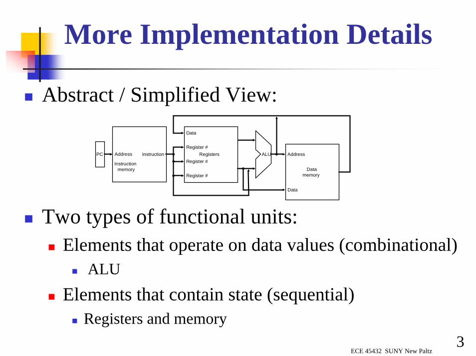
Abstract / Simplified View:
Two types of functional units:Elements that operate on data values (combinational)
ALU
Elements that contain state (sequential)Registers and memory
RegistersRegister #
Data
Register #
Data�memory
Address
Data
Register #
PC Instruction ALU
Instruction�memory
Address
ECE 45432 SUNY New Paltz4
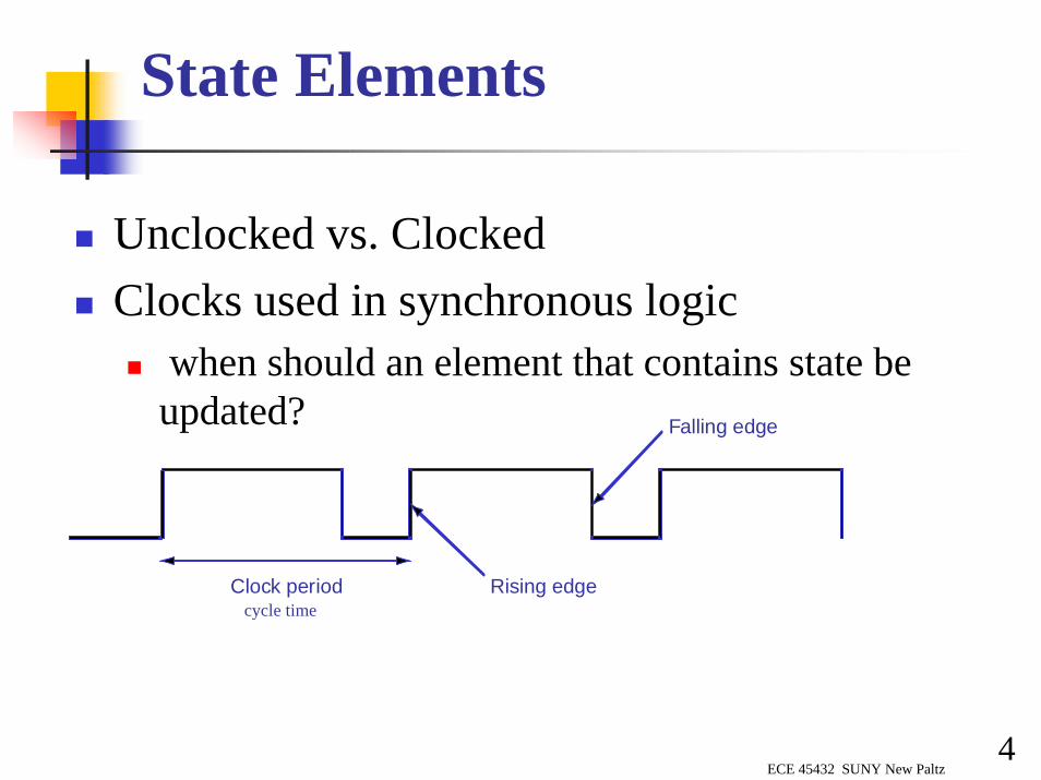
Unclocked vs. ClockedClocks used in synchronous logic
when should an element that contains state be updated?
State Elements
Clock period Rising edge
Falling edge
cycle time
ECE 45432 SUNY New Paltz5
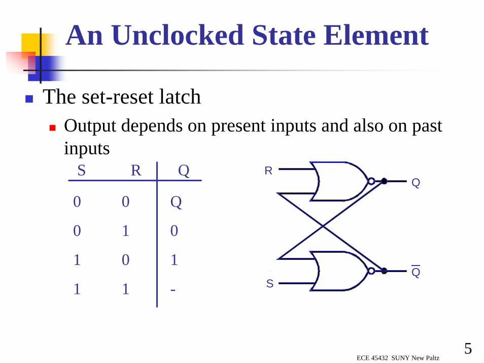
An Unclocked State Element
The set-reset latchOutput depends on present inputs and also on past inputs
S R Q R
S
Q
Q
0 0 Q
0 1 0
1 0 1
1 1 -
ECE 45432 SUNY New Paltz6
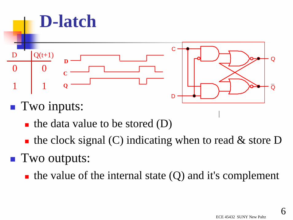
Two inputs:the data value to be stored (D)the clock signal (C) indicating when to read & store D
Two outputs:the value of the internal state (Q) and it's complement
D-latch
Q
C
D
_Q
D Q(t+1)
0 0
1 1
D
C
Q

ECE 45432 SUNY New Paltz7
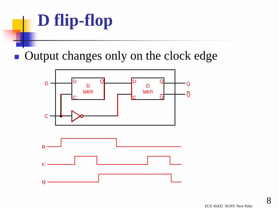
Latches and Flip-flops
Output is equal to the stored value inside the element(don't need to ask for permission to look at the value)Change of state (value) is based on the clock
Latches: whenever the clock is asserted (high or low) and the input changesFlip-flop: whenever the clock is asserted (low to high or high to low transition) and the input changes (edge-triggered methodology)
Note:"logically true“ could mean electrically low
ECE 45432 SUNY New Paltz8
D flip-flop
Output changes only on the clock edge
D
C
Dlatch
D
C
QD
latch
D
C
Q Q
Q Q
D
C
Q
ECE 45432 SUNY New Paltz9
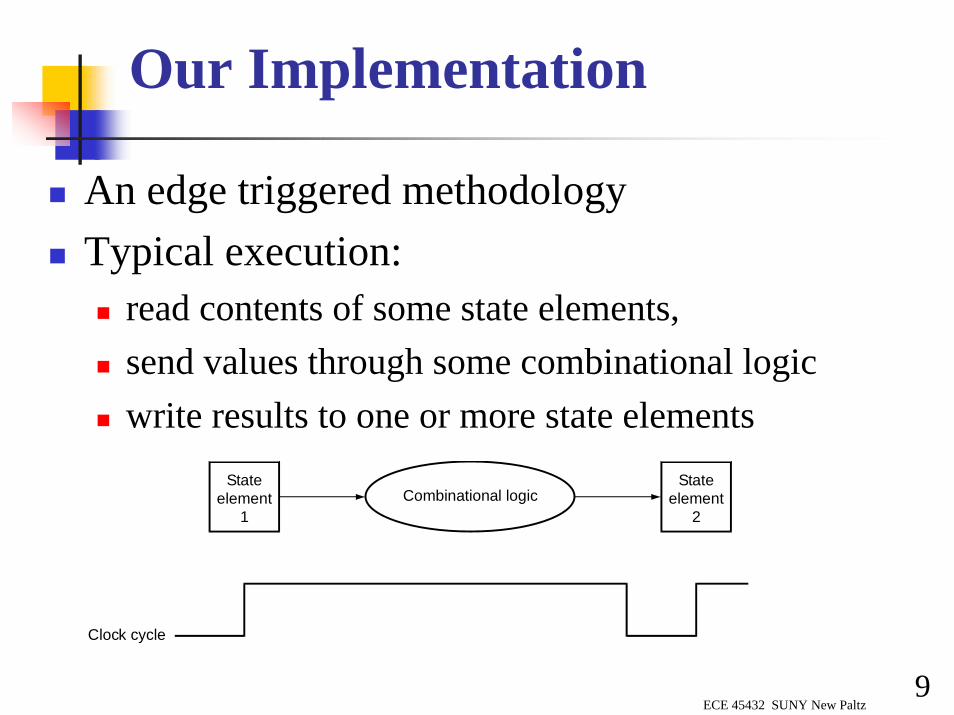
Our Implementation
An edge triggered methodologyTypical execution:
read contents of some state elements, send values through some combinational logicwrite results to one or more state elements
Stateelement
1
Stateelement
2Combinational logic
Clock cycle

ECE 45432 SUNY New Paltz10
Clocking Methodology A clocking methodology defines when signals can be read and written
wouldn't want to read a signal at the same time it was being written
All storage elements are clocked by the same clock edgeCycle Time
CLK-to-Q + Longest Delay Path + Setup + Clock Skew(CLK-to-Q + Shortest Delay Path - Clock Skew) > Hold Time
Clk
Don’t Care
Setup Hold
.
.
.
.
.
.
.
.
.
.
.
.
Setup Hold

ECE 45432 SUNY New Paltz11
Abstraction
Make sure you understand the abstractions!Sometimes it is easy to think you do, when you don’t
Mux
Select
B31
A31
C31
Mux
B30
A30
C30
Mux
B0
A0
C0
......
Mux
C
Select
32
32
32
B
A

ECE 45432 SUNY New Paltz12
Register File
Read operation using D flip-flops and MUX’s
Read registernumber 1 Read
data 1Read registernumber 2
Readdata 2
Writeregister
WriteWritedata
Register file
Read registernumber 1
Register 0
Register 1
. . .
Register n – 2
Register n – 1
Mux
Read registernumber 2
Mux
Read data 1
Read data 2
What is the function of “Mux” above?

ECE 45432 SUNY New Paltz13
Register File – Read and Write
M�u�x
Register 0Register 1
Register n – 1Register n
M�u�x
Read data 1
Read data 2
Read register�number 1
Read register�number 2
Read registernumber 1 Read
data 1Read registernumber 2
Readdata 2
Writeregister
WriteWritedata
Register file
n-to-1decoder
Register0
Register1
Registern– 1C
C
D
DRegistern
C
C
D
D
01
n– 1n
Write
Write Register
Write Data
How many registers can we read and write at the same time?
Does this support MIPS instructions requirements?

ECE 45432 SUNY New Paltz14
Building the Datapath
Include the functional units we need for each instruction
Use multiplexors to stitch them together
ALU Control:000 AND001 OR010 add110 subtract111 set-on-less-than
A LU control
R egW rite
R eg is te rsW riteregister
R eaddata 1
R eaddata 2
R eadregister 1
R eadregister 2
W rited ata
A LUresu lt
ALU
D ata
D ata
R eg is te rnum bers
a . R egisters b. A LU
Zero5
5
5 3
PC
Instructionmemory
Instructionaddress
Instruction
a. Instruction memory b. Program counter
Add Sum
c. Adder
16 32Sign�
extend
b. Sign-extension unit
MemRead
MemWrite
Data�memory
Write�data
Read�data
a. Data memory unit
Address

ECE 45432 SUNY New Paltz15
Datapath for Fetch and R-Instructions
Portion of datapath for fetching instructions and updating PC
R-format instructions: read two registers and write one register
PC
Instructionmemory
Readaddress
Instruction
4
Add
ALU control
RegWrite
RegistersWriteregister
Readdata 1
Readdata 2
Readregister 1
Readregister 2
Writedata
ALUresult
ALUZero
3
Instruction
ALU Control:000 AND001 OR010 add110 subtract111 set-on-less-than
ECE 45432 SUNY New Paltz16
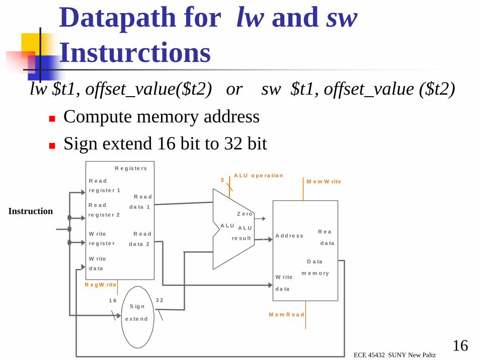
Datapath for lw and swInsturctions
lw $t1, offset_value($t2) or sw $t1, offset_value ($t2)Compute memory addressSign extend 16 bit to 32 bit
1 6 3 2
R e g is te rs
W rite
re g is te r
W rite
d a ta
R e a d
d a ta 1
R e a d
d a ta 2
R e a d
re g is te r 1
R e a d
re g is te r 2
A L U o p e ra tio n3
R e g W rite
M e m R e a d
M e m W rite
A L U
re su lt
Z e ro
A L U
D a ta
m e m o ry
A d d re s s
W rite
d a ta
R e a
d a ta
S ig n
e x te n d
Instruction

ECE 45432 SUNY New Paltz17
Building beq Instruction
beq $t1, $t2, offsetCompare registers, use ALU to affect Z flagIf not equal, next PC <= PC +4If equal, sign extend the offset and shift by two
Instruction
16 32
Add ALUresult
Registers
W riteregister
W ritedata
R eaddata 1
Readdata 2
Readregister 1R eadregister 2
Shiftleft 2
ALU operation3
RegW rite
Z eroALU
PC + 4
Branch control
Next instruction address
Signextend

ECE 45432 SUNY New Paltz18
A Simple Implementation of aDatapath
Covers: lw, sw, beq, add, sub, and, or, set-on-less-thanUse multiplexors to stitch them together
Instruction
16 32
Registers
Writeregister
Writedata
Readdata 1
Readdata 2
Readregister 1
Readregister 2
Mux
ALU operation3
RegWrite
MemRead
MemWriteALUSrc
MemtoReg
ALUresult
ZeroALU
Datamemory
Address
Writedata
Readdata M
ux
Signextend

ECE 45432 SUNY New Paltz19
Implementation of the Datapath
PC
Instructionmemory
Readaddress
Instruction
16 32
Add ALUresult
Mux
Registers
WriteregisterWritedata
Readdata1
Readdata2
Readregister1Readregister2
Shiftleft2
4
Mux
ALUoperation3
RegWrite
MemRead
MemWrite
PCSrc
ALUSrcMemtoReg
ALUresult
ZeroALU
Datamemory
Address
Writedata
Readdata M
ux
Signextend
Add

ECE 45432 SUNY New Paltz20
Three Instruction Classes• R-Type Instruction
op rs rt rd shamt funct
rd: destination
•Load and Store Instructions
op rs rt 16 bit offset
rt: destination
•Branch Instruction
op rs rt 16 bit offset
rt: destination
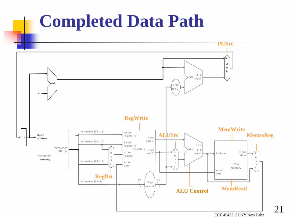
ECE 45432 SUNY New Paltz21
Completed Data Path
MemtoRegP C
Instructionmemory
Readadd ress
Ins truc tion[31– 0 ]
Instruction [20– 16 ]
Instruction [25– 21 ]
A dd
4
16 32Instruction [15– 0]
0
0Mux
0
1
Add ALUresu lt
Mux
0
1
Regis tersW riteregister
W riteda ta
Readda ta 1
Readda ta 2
R eadregister 1
R eadregister 2
Signextend
S hiftle ft 2
Mux
1
ALUresult
Zero
Datam em ory
W ritedata
Readda ta
Mux
1
Instruction [15– 11 ]
A LUAddress
RegWrite
ALUSrc
MemRead
RegDst
MemWrite
PCSrc
ALU Control
ECE 45432 SUNY New Paltz22
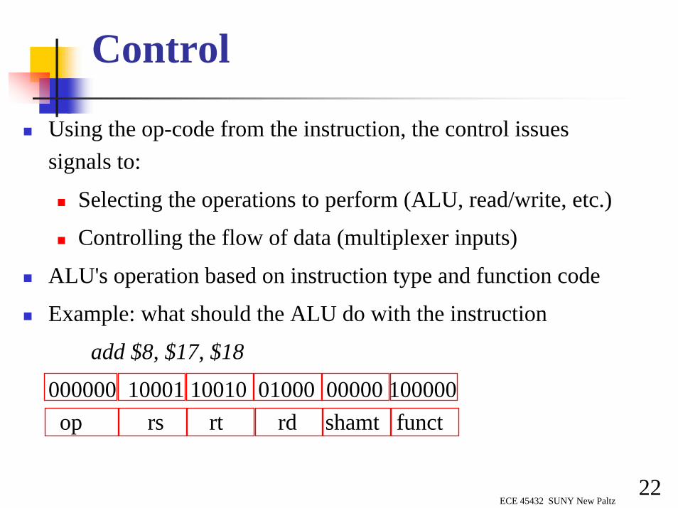
Control
Using the op-code from the instruction, the control issues signals to:
Selecting the operations to perform (ALU, read/write, etc.)
Controlling the flow of data (multiplexer inputs)
ALU's operation based on instruction type and function code
Example: what should the ALU do with the instruction
add $8, $17, $18
000000 10001 10010 01000 00000 100000op rs rt rd shamt funct
ECE 45432 SUNY New Paltz23
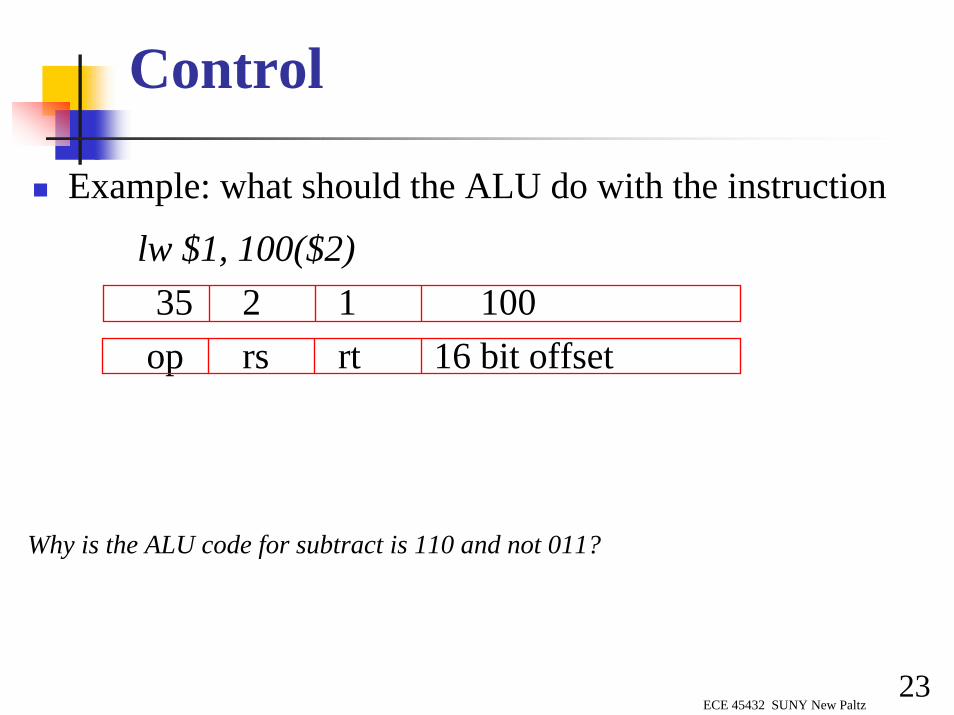
Control
Example: what should the ALU do with the instruction
lw $1, 100($2)35 2 1 100op rs rt 16 bit offset
Why is the ALU code for subtract is 110 and not 011?
ECE 45432 SUNY New Paltz24
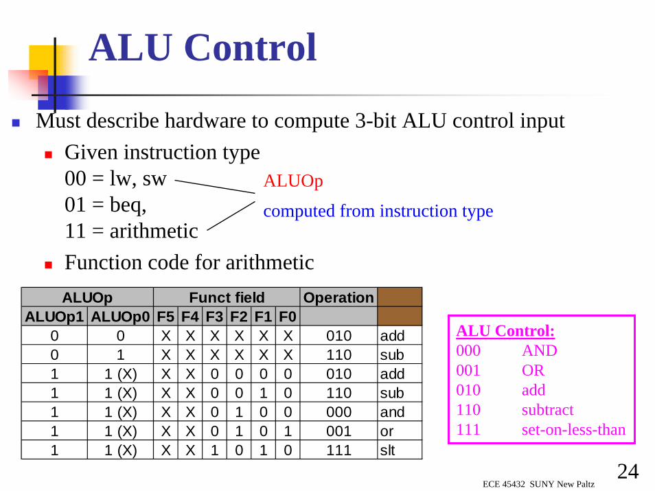
ALU Control
Must describe hardware to compute 3-bit ALU control inputGiven instruction type 00 = lw, sw01 = beq, 11 = arithmeticFunction code for arithmeticALUOp Funct field Operation
ALUOp1 ALUOp0 F5 F4 F3 F2 F1 F00 0 X X X X X X 010 add0 1 X X X X X X 110 sub1 1 (X) X X 0 0 0 0 010 add1 1 (X) X X 0 0 1 0 110 sub1 1 (X) X X 0 1 0 0 000 and1 1 (X) X X 0 1 0 1 001 or1 1 (X) X X 1 0 1 0 111 slt
ALU Control:000 AND001 OR010 add110 subtract111 set-on-less-than
ALUOp
computed from instruction type

ECE 45432 SUNY New Paltz25
ALU Control
Operation2
Operation1
Operation0
Operation
ALUOp1
F3
F2
F1
F0
F (5–0)
ALUOp0
ALUOp
ALUcontrol blockMuli-level decoding can reduce size of control unit and increase its speed.
ALUOp Funct field OperationALUOp1 ALUOp0 F5 F4 F3 F2 F1 F0 2 1 0
0 0 X X X X X X 010 add0 1 X X X X X X 110 sub1 0 X X 0 0 0 0 010 add1 0 X X 0 0 1 0 110 sub1 0 X X 0 1 0 0 000 and1 0 X X 0 1 0 1 001 or1 0 X X 1 0 1 0 111 slt
Inputs Outputs

ECE 45432 SUNY New Paltz26
A Simple Control
P C
Instructionmemory
Readadd ress
Ins truc tion[31– 0 ]
Instruction [20– 16 ]
Instruction [25– 21 ]
A dd
Instruction [5– 0]
4
16 32Instruction [15– 0]
0
0Mux
0
1
Add ALUresu lt
Mux
0
1
Regis tersW riteregister
W riteda ta
Readda ta 1
Readda ta 2
R eadregister 1
R eadregister 2
Signextend
S hiftle ft 2
Mux
1
ALUresult
Zero
Datam em ory
W ritedata
Readda ta
Mux
1
Instruction [15– 11 ]
A LUcontrol
A LUAddress
RegWrite
ALUSrc
ALUop
MemRead
MemtoReg
RegDst
MemWrite
PCSrc

ECE 45432 SUNY New Paltz27
Control
Instruction Opcode RegDst ALUSrcMemto-
RegReg
WriteMem Read
Mem Write Branch ALUOp1ALUOp0
R-format 00 0000 1 0 0 1 0 0 0 1 0lw 10 0011 0 1 1 1 1 0 0 0 0sw 10 1011 X 1 X 0 0 1 0 0 0beq 00 0100 X 0 X 0 0 0 1 0 1
PC
Instruction�memory
Read�address
Instruction�[31– 0]
Instruction [20– 16]
Instruction [25– 21]
Add
Instruction [5– 0]
MemtoRegALUOpMemWrite
RegWrite
MemReadBranchRegDst
ALUSrc
Instruction [31– 26]
4
16 32Instruction [15– 0]
0
0M�u�x
0
1
Control
Add ALU�result
M�u�x
0
1
RegistersWrite�register
Write�data
Read�data 1
Read�data 2
Read�register 1
Read�register 2
Sign�extend
Shift�left 2
M�u�x
1
ALU�result
Zero
Data�memory
Write�data
Read�data
M�u�x
1
Instruction [15– 11]
ALU�control
ALUAddress

ECE 45432 SUNY New Paltz28
Single Cycle Control
Simple combinational logic
R-format Iw sw beq
Op0Op1Op2Op3Op4Op5
Inputs
Outputs
RegDst
ALUSrcMemtoReg
RegWrite
MemReadMemWrite
BranchALUOp1
ALUOpO
Operation2
Operation1
Operation0
Operation
ALUOp1
F3
F2
F1
F0
F (5–0)
ALUOp0
ALUOp
ALUcontrol block

ECE 45432 SUNY New Paltz29
Our Simple Control Structure
All of the logic is combinational
We wait for everything to settle down, and the right thing to be done
ALU might not produce “right answer” right away
we use write signals along with clock to determine when to write
Cycle time determined by length of the longest path
Combinational logicContent of PC Content
of PC
Clock

ECE 45432 SUNY New Paltz30
Single Cycle Implementation
Calculate cycle time assuming negligible delays except:memory (2ns), ALU and adders (2ns), register file access (1ns)
MemtoReg
MemRead
MemWriteALUSrc
RegDst
PC
Instructionmemory
Readaddress
Instruction[31–0]
Instruction[20–16]
Instruction[25–21]
Add
Instruction[5–0]
RegWrite
4
16 32Instruction[15–0]
0Registers
WriteregisterWritedata
Writedata
Readdata 1
Readdata 2
Readregister 1Readregister 2
Signextend
ALUresult
Zero
Datamemory
Address Readdata M
ux
1
0
Mux
1
Mux
1
0
Mux
1
Instruction[15–11]
Shiftleft 2
PCSrc
ALU
Add ALUresult
ALUOp
0
ALUcontrol

ECE 45432 SUNY New Paltz31
Single Cycle ImplementationCalculate cycle time assuming negligible delays except:
memory (2ns), ALU and adders (2ns), register file access (1ns)
M e m t o R e g
M e m R e a d
M e m W r i te
A L U O p
A L U S rc
R e g D s t
P C
I n s t ru c t io n �m e m o ry
R e a d �a d d re s s
In s tru c t io n �[3 1 – 0 ]
In s tr u c t io n [2 0 – 1 6 ]
In s tr u c t io n [2 5 – 2 1 ]
A d d
I n s tru c t io n [5 – 0 ]
R e g W r i te
4
1 6 3 2In s tr u c t io n [1 5 – 0 ]
0R e g is t e rs
W r ite �re g is te rW r ite �d a ta
W r i te �d a ta
R e a d �d a ta 1
R e a d �d a ta 2
R e a d �re g is te r 1R e a d �re g is te r 2
S ig n �e x te n d
A L U �re s u l t
Z e r o
D a ta �m e m o ry
A d d re s s R e a d �d a ta M �
u �x
1
0
M �u �x
1
0
M �u �x
1
0
M �u �x
1
In s tr u c t io n [1 5 – 1 1 ]
A L U �c o n t ro l
S h i f t�le f t 2
P C S rc
A L U
A d d A L U �re s u lt
InstructionInstr.
MemoryRegister
ReadALU Op.
Data Memory
Reg. Write Total
R-format 2 1 2 0 1 6 nslw 2 1 2 2 1 8 nssw 2 1 2 2 7 nsbeq 2 1 2 5 ns

ECE 45432 SUNY New Paltz32
Single Cycle Problems:
Cycle time should accommodate the longest instruction.
What if we had more complicated instructions like floating point?
Can use a unit only once during a cycleMay need multiple copies of some functional units (wasteful of area)
One Solution:use a “smaller” cycle timehave different instructions take different numbers of cyclesa “multi-cycle” datapath:
ECE 45432 SUNY New Paltz33
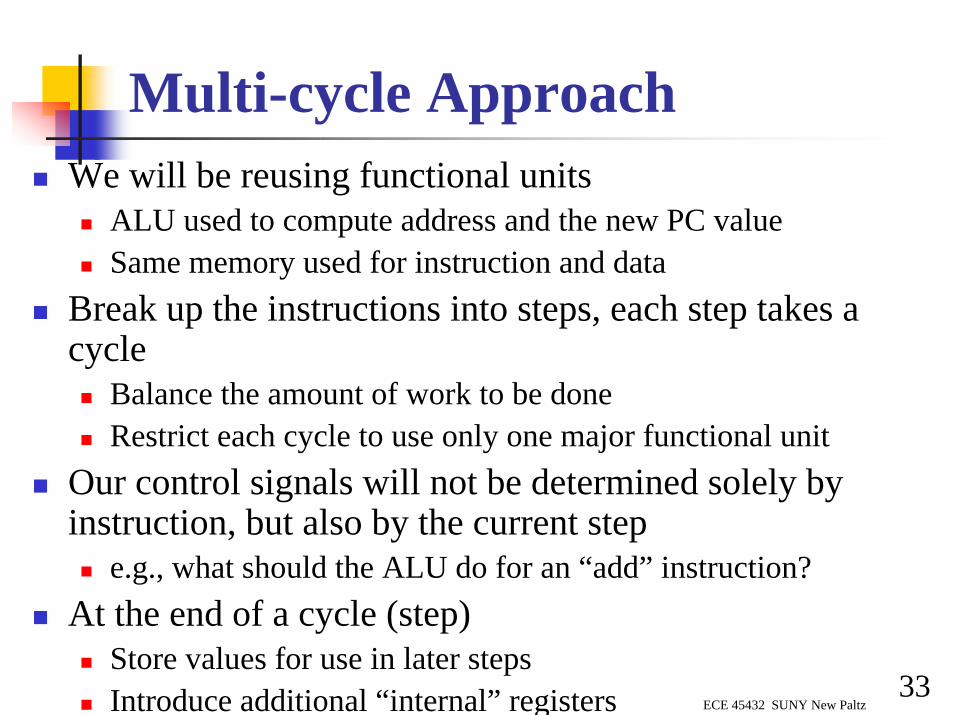
Multi-cycle ApproachWe will be reusing functional units
ALU used to compute address and the new PC valueSame memory used for instruction and data
Break up the instructions into steps, each step takes a cycle
Balance the amount of work to be doneRestrict each cycle to use only one major functional unit
Our control signals will not be determined solely by instruction, but also by the current step
e.g., what should the ALU do for an “add” instruction?At the end of a cycle (step)
Store values for use in later steps Introduce additional “internal” registers
ECE 45432 SUNY New Paltz34
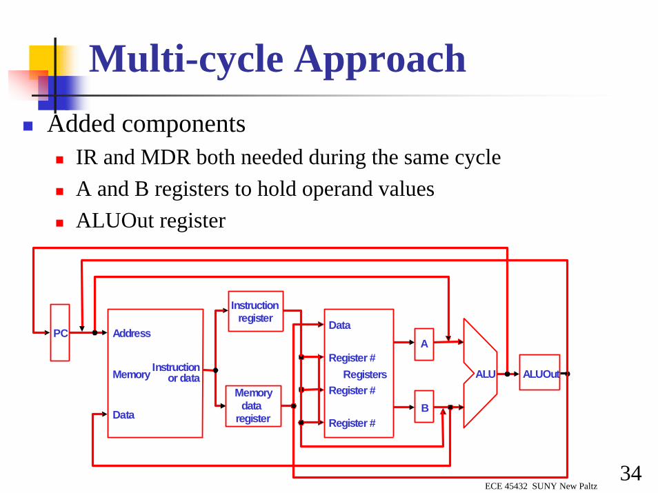
Multi-cycle ApproachAdded components
IR and MDR both needed during the same cycleA and B registers to hold operand valuesALUOut register
PC
Memory
Address
Instructionor data
Data
Instructionregister
RegistersRegister #
Data
Register #
Register #
ALUMemory
dataregister
A
B
ALUOut
ECE 45432 SUNY New Paltz35
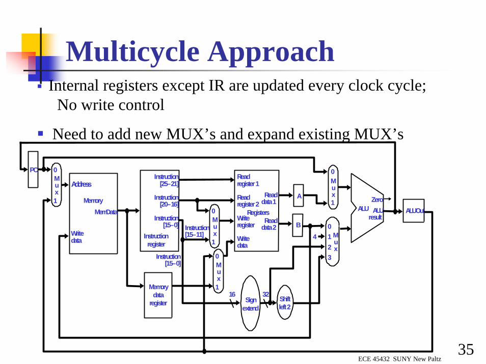
Multicycle Approach
Shiftleft2
PC
MemoryMemData
Writedata
Mux
0
1
RegistersWriteregister
Writedata
Readdata1
Readdata2
Readregister1
Readregister2
Mux
0
1
Mux
0
1
4
Instruction[15–0]
Signextend
3216
Instruction[25–21]
Instruction[20–16]
Instruction[15–0]
Instructionregister
1 Mux
0
32
Mux
ALUresult
ALUZero
Memorydata
register
Instruction[15–11]
A
B
ALUOut
0
1
Address
Internal registers except IR are updated every clock cycle; No write control
Need to add new MUX’s and expand existing MUX’s
ECE 45432 SUNY New Paltz36
Shiftleft2
PC
MemoryMemData
Writedata
Mux
0
1
RegistersWriteregister
Writedata
Readdata1
Readdata2
Readregister1
Readregister2
Mux
0
1
Mux
0
1
4
Instruction[15–0]
Signextend
3216
Instruction[25–21]
Instruction[20–16]
Instruction[15–0]
Instructionregister
1 Mux
0
32
Mux
ALUresult
ALUZero
Memorydata
register
Instruction[15–11]
A
B
ALUOut
0
1
Address
Shiftleft2
01
2
3226
ALUcontrol
ALUOp
ALUSrcB
ALUSrcA
PCSource
MemtoReg
REGWriteIRWriteMemWriteMemRead
IorD
PCWrite
REGDst
PCWriteCondZero (ALU)
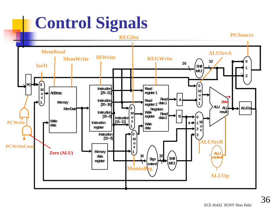
Control Signals

ECE 45432 SUNY New Paltz37
Instructions from ISA PerspectiveConsider each instruction from perspective of ISA.Example:
The add instruction changes a register. Register specified by bits 15:11 of instruction. Instruction specified by the PC. New value is the sum (“op”) of two registers. Registers specified by bits 25:21 and 20:16 of the instruction
Reg[Memory[PC][15:11]] <= Reg[Memory[PC][25:21]] op Reg[Memory[PC][20:16]]
In order to accomplish this we must break up the instruction.(kind of like introducing variables when programming)
ECE 45432 SUNY New Paltz38
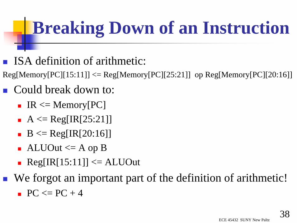
Breaking Down of an Instruction
ISA definition of arithmetic:Reg[Memory[PC][15:11]] <= Reg[Memory[PC][25:21]] op Reg[Memory[PC][20:16]]
Could break down to:IR <= Memory[PC]A <= Reg[IR[25:21]]B <= Reg[IR[20:16]]ALUOut <= A op BReg[IR[15:11]] <= ALUOut
We forgot an important part of the definition of arithmetic!PC <= PC + 4
ECE 45432 SUNY New Paltz39
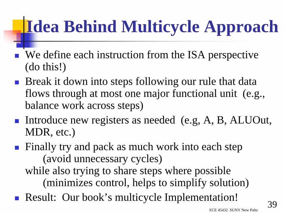
Idea Behind Multicycle ApproachWe define each instruction from the ISA perspective (do this!)Break it down into steps following our rule that data flows through at most one major functional unit (e.g., balance work across steps)Introduce new registers as needed (e.g, A, B, ALUOut, MDR, etc.)Finally try and pack as much work into each step
(avoid unnecessary cycles)while also trying to share steps where possible
(minimizes control, helps to simplify solution)Result: Our book’s multicycle Implementation!
ECE 45432 SUNY New Paltz40
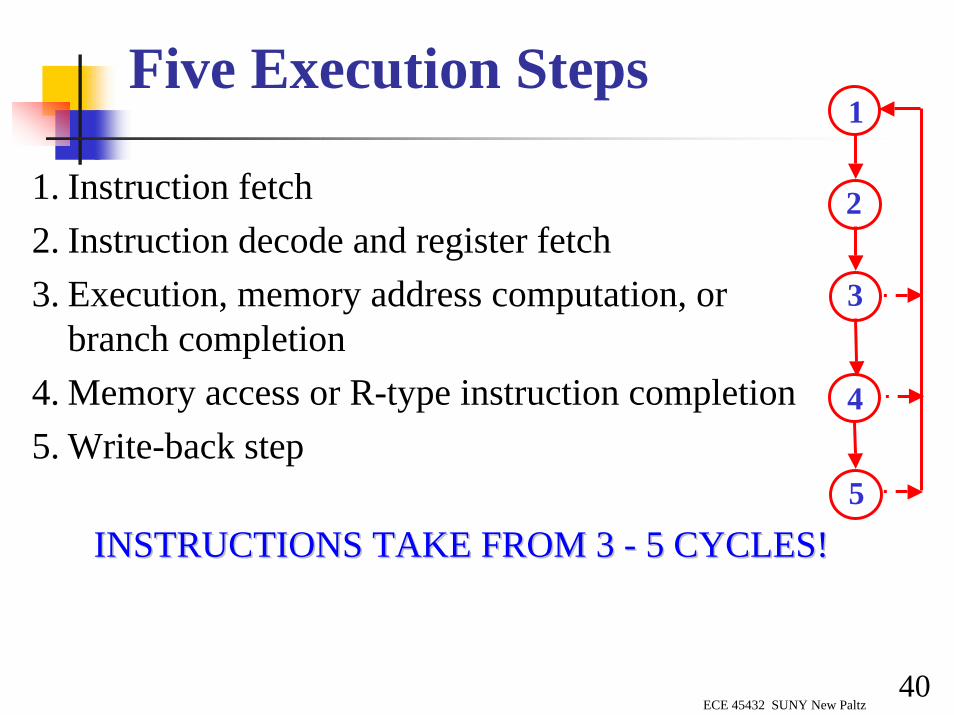
1. Instruction fetch2. Instruction decode and register fetch3. Execution, memory address computation, or
branch completion4. Memory access or R-type instruction completion5. Write-back step
INSTRUCTIONS TAKE FROM 3 INSTRUCTIONS TAKE FROM 3 -- 5 CYCLES!5 CYCLES!
Five Execution Steps1
2
3
4
5

ECE 45432 SUNY New Paltz41
Step 1: Instruction Fetch 1
Use PC to get instruction and put it in the Instruction Register.Increment the PC by 4 and put the result back in the PC
using RTL "Register-Transfer Language"IR <= Memory[PC];PC <= PC + 4;
MemReadALUSrcA =0IorD = 0IRWriteALUSrcB = 01ALUOp = 00PCWritePCSource = 00
Shiftleft2
PC
MemoryMemData
Writedata
Mux
0
1RegistersWriteregister
Writedata
Readdata1Readdata2
Readregister1Readregister2
Mux
0
1
Mux
0
1
4Instruction[15–0]
Signextend
3216
Instruction[25–21]Instruction[20–16]Instruction[15–0]
Instructionregister 1Mux
0
32
MuxALUresult
ALUZero
Memorydataregister
Instruction[15–11]
A
BALUOut
0
1Address
Shiftleft2012
3226
ALUcontrol
ALUOpALUSrcB
ALUSrcA
PCSource
MemtoReg
REGWriteIRWriteMemWriteMemRead
IorD
PCWrite
REGDst
PCWriteCondZero (ALU)
ECE 45432 SUNY New Paltz42
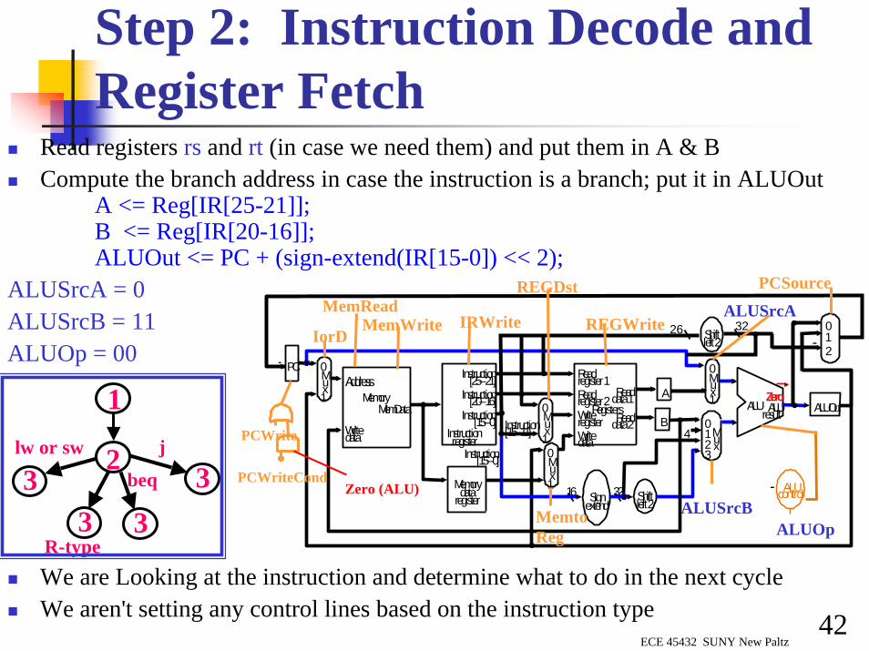
Step 2: Instruction Decode and Register Fetch
Read registers rs and rt (in case we need them) and put them in A & BCompute the branch address in case the instruction is a branch; put it in ALUOut
A <= Reg[IR[25-21]];B <= Reg[IR[20-16]];ALUOut <= PC + (sign-extend(IR[15-0]) << 2);
ALUSrcA = 0ALUSrcB = 11ALUOp = 00
We are Looking at the instruction and determine what to do in the next cycleWe aren't setting any control lines based on the instruction type
Shiftleft2
PC
MemoryMemData
Writedata
Mux
0
1RegistersWriteregister
Writedata
Readdata1Readdata2
Readregister1Readregister2
Mux
0
1
Mux
0
1
4Instruction[15–0]
Signextend
3216
Instruction[25–21]Instruction[20–16]Instruction[15–0]
Instructionregister 1Mux
0
32
MuxALUresult
ALUZero
Memorydataregister
Instruction[15–11]
A
BALUOut
0
1Address
Shiftleft2012
3226
ALUcontrol
ALUOpALUSrcB
ALUSrcA
PCSource
MemtoReg
REGWriteIRWriteMemWriteMemRead
IorD
PCWrite
REGDst
PCWriteCondZero (ALU)
1
23
3 33
jlw or sw
beq
R-type

ECE 45432 SUNY New Paltz43
Step 3: Instruction DependentALU is performing one of three functions, based on instruction type(ignore j instruction for now)
Memory Reference: (lw or sw) R-type: Branch: beqALUOut <= A + sign-extend(IR[15-0]); ALUOut <= A op B; if (A==B) PC <= ALUOut
(compute address) (execute) (complete branch)
ALUSrcA = 1 ALUSrcA = 1 ALUSrcA = 1ALUSrcB = 10 ALUSrcB = 00 ALUSrcB = 00ALUOp = 00 ALUOp = 10 ALUOp = 01
go to step 4 PCWriteCondPCSource = 01
lw swend of execution fetch next instruction
ECE 45432 SUNY New Paltz44
Shiftleft2
PC
Memory
MemData
Writedata
Mux
0
1
RegistersWriteregister
Writedata
Readdata1
Readdata2
Readregister 1
Readregister 2
Mux
0
1
Mux
0
1
4
Instruction[15–0]
Signextend
3216
Instruction[25–21]
Instruction[20–16]
Instruction[15–0]
Instructionregister
1 Mux
0
32
Mux
ALUresult
ALUZero
Memorydata
register
Instruction[15–11]
A
B
ALUOut
0
1
Address
Shiftleft2
01
2
3226
ALUcontrol
ALUOp
ALUSrcB
ALUSrcA
PCSource
MemtoReg
REGWriteIRWriteMemWriteMemRead
IorD
PCWrite
REGDst
PCWriteCondZero (ALU)
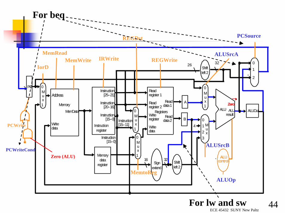
For lw and sw
For beq

ECE 45432 SUNY New Paltz45
Step 4: R-type or Memory Access
Lw sw R-type
MDR = Memory[ALUOut]; Memory[ALUOut] = B; Reg[IR[15-11]] = ALUOut;
(read from memory) (write to memory) (store result)MemRead MemWrite RegDst = 1IorD = 1 IorD = 1 REGWrite
MemtoReg = 0
end of execution end of execution fetch next instruction fetch next instruction

ECE 45432 SUNY New Paltz46
PCSource
Shiftleft2
PC
Memory
MemData
Writedata
Mux
0
1
RegistersWriteregister
Writedata
Readdata1
Readdata2
Readregister 1
Readregister 2
Mux
0
1
Mux
0
1
4
Instruction[15–0]
Signextend
3216
Instruction[25–21]
Instruction[20–16]
Instruction[15–0]
Instructionregister
1 Mux
0
32
Mux
ALUresult
ALUZero
Memorydata
register
Instruction[15–11]
A
B
ALUOut
0
1
Address
Shiftleft2
01
2
2826
ALUcontrol
ALUOp
ALUSrcB
ALUSrcA
MemtoReg
REGWriteIRWriteMemWriteMemRead
IorD
PCWrite
REGDst
PCWriteCondZero (ALU)
lw sw
R-type
32
ECE 45432 SUNY New Paltz47
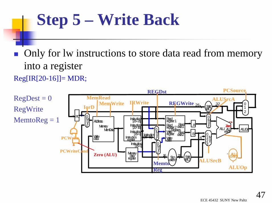
Step 5 – Write Back
Only for lw instructions to store data read from memory into a register
Reg[IR[20-16]]= MDR;
RegDest = 0RegWriteMemtoReg = 1
Shiftleft2
PC
MemoryMemData
Writedata
Mux
0
1RegistersWriteregister
Writedata
Readdata1Readdata2
Readregister1Readregister2
Mux
0
1
Mux
0
1
4Instruction[15–0]
Signextend
3216
Instruction[25–21]Instruction[20–16]Instruction[15–0]
Instructionregister 1Mux
0
32
MuxALUresult
ALUZero
Memorydataregister
Instruction[15–11]
A
BALUOut
0
1Address
Shiftleft2012
3226
ALUcontrol
ALUOpALUSrcB
ALUSrcA
PCSource
MemtoReg
REGWriteIRWriteMemWriteMemRead
IorD
PCWrite
REGDst
PCWriteCondZero (ALU)

ECE 45432 SUNY New Paltz48
Control Summary
Step nameAction for R-type
instructionsAction for memory-reference
instructionsAction for branches
Action for jumps
Instruction fetch IR = Memory[PC]PC = PC + 4
Instruction A = Reg [IR[25-21]]decode/register fetch B = Reg [IR[20-16]]
ALUOut = PC + (sign-extend (IR[15-0]) << 2)Execution, address ALUOut = A op B ALUOut = A + sign-extend if (A ==B) then PC = PC [31-28] IIcomputation, branch/ (IR[15-0]) PC = ALUOut (IR[25-0]<<2)jump completionMemory access or R-type Reg [IR[15-11]] = Load: MDR = Memory[ALUOut]completion ALUOut or
Store: Memory [ALUOut] = B
Memory read completion Load: Reg[IR[20-16]] = MDR

ECE 45432 SUNY New Paltz49
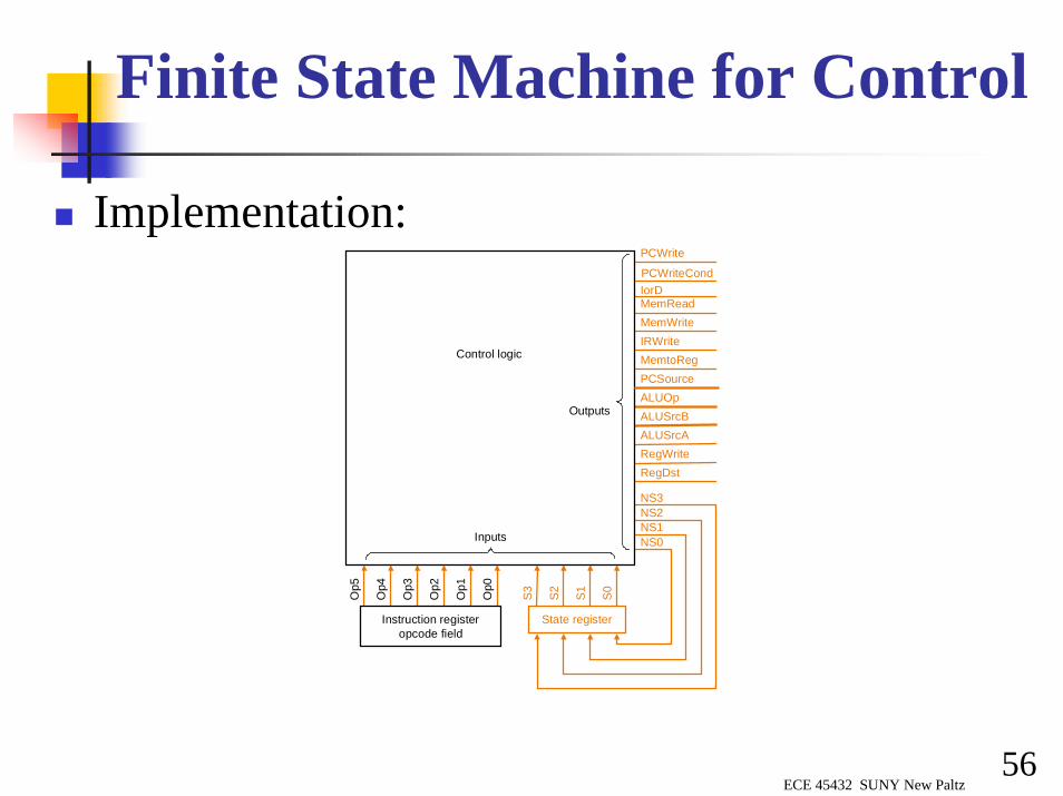
Implementing the Control
Value of control signals is dependent upon:what instruction is being executedwhich step is being performed
Use the information we’ve accumulated to specify a finite state machine
specify the finite state machine graphically, oruse microprogramming
Implementation can be derived from specification

ECE 45432 SUNY New Paltz50
Review: Finite State Machines
Finite state machines:A set of states and Next state function (determined by current state and the input)Output function (determined by current state and possibly input)
We’ll use a Moore machine (output based only on current state)How does Moore machine various from Mealy machine?
Inputs
Current state
Outputs
Clock
Next-statefunction
Outputfunction
Nextstate
ECE 45432 SUNY New Paltz51
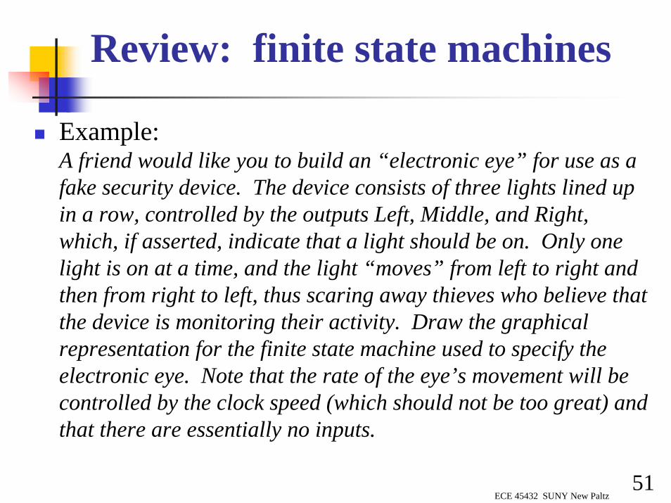
Review: finite state machines
Example: A friend would like you to build an “electronic eye” for use as a fake security device. The device consists of three lights lined up in a row, controlled by the outputs Left, Middle, and Right, which, if asserted, indicate that a light should be on. Only one light is on at a time, and the light “moves” from left to right and then from right to left, thus scaring away thieves who believe that the device is monitoring their activity. Draw the graphical representation for the finite state machine used to specify the electronic eye. Note that the rate of the eye’s movement will be controlled by the clock speed (which should not be too great) and that there are essentially no inputs.

Graphical Specification of FSM
PCWritePCSource = 10
ALUSrcA = 1ALUSrcB = 00ALUOp = 01PC WriteCond
PCSource = 01
ALUSrcA = 1ALUSrcB = 00
ALUOp = 10
RegDst = 1RegWrite
MemtoReg = 0MemWriteIorD = 1
MemReadIorD = 1
ALUSrcA = 1ALUSrcB = 10ALUOp = 00
R egDst = 0RegWrite
MemtoReg = 1
ALUSrcA = 0ALUSrcB = 11ALUOp = 00
MemReadALUSrcA = 0
IorD = 0IRWrite
ALUSrcB = 01ALUOp = 00
PCWritePCSource = 00
Instruction fe tchInstruction decode/
register fetch
Jumpcompletion
BranchcompletionExecution
M emory addresscomputation
Memoryaccess
Memoryaccess R-type completion
W rite-back step
(Op = 'LW ') or (Op = 'SW ') (Op = R-type)
(Op =
'BEQ')
(Op
='J
' )
(Op= 'SW
')
(Op
='L
W' )
4
01
9862
753
Start
don’t care if not mentioned
asserted if name only
otherwise exact value
How many state bits will we need?
ECE 45432 SUNY New Paltz53
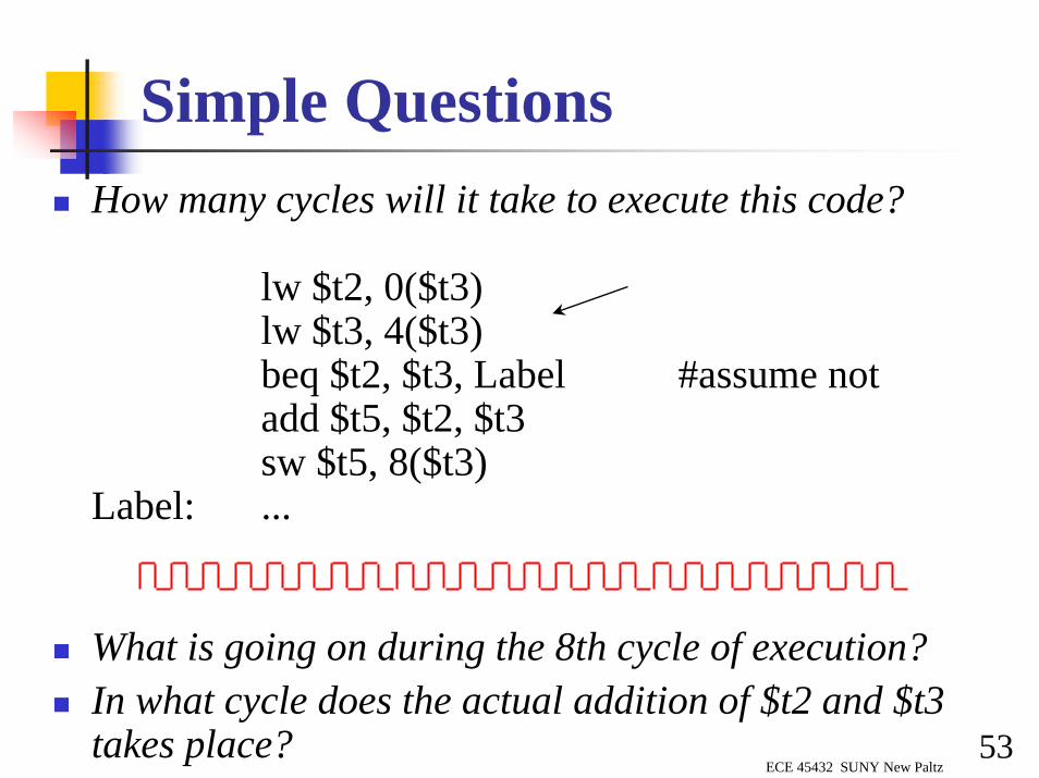
Simple QuestionsHow many cycles will it take to execute this code?
lw $t2, 0($t3)lw $t3, 4($t3)beq $t2, $t3, Label #assume notadd $t5, $t2, $t3sw $t5, 8($t3)
Label: ...
What is going on during the 8th cycle of execution?In what cycle does the actual addition of $t2 and $t3 takes place?
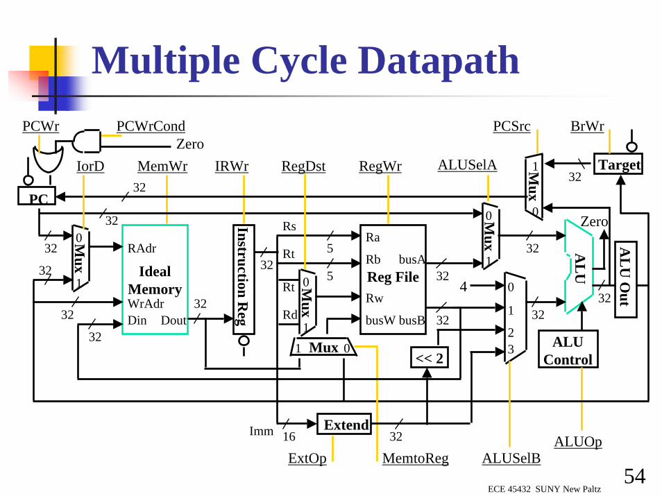
ECE 45432 SUNY New Paltz54
Multiple Cycle Datapath
IdealMemoryWrAdrDin
RAdr
32
32
32Dout
MemWr32
AL
U
3232
ALUOp
ALUControl
InstructionR
eg
32
IRWr
32
Reg File
Ra
Rw
busW
Rb5
5
32busA
32busB
RegWr
Rs
Rt
Mux
0
1
Rt
Rd
PCWr
ALUSelA
Mux 01
RegDst
Mux
0
1
32
PC
MemtoReg
Extend
ExtOp
Mux
0
132
0
1
23
4
16Imm 32
<< 2
ALUSelB
Mux
1
0
Target32
Zero
ZeroPCWrCond PCSrc BrWr
32
IorD
AL
U O
ut

Readregister 1
Readregister 2
Writeregister
Writedata
Registers ALUZero
Readdata 1
Readdata 2
Signextend
16 32
Instruction[31–26]
Instruction[25–21]
Instruction[20–16]
Instruction[15–0]
ALUresult
Mux
Mux
Shiftleft 2
Shiftleft 2
Instructionregister
PC 0
1
Mux
0
1
Mux
0
1
Mux
0
1A
B 0123
Mux
0
1
2
ALUOut
Instruction[15–0]
Memorydata
register
Address
Writedata
MemoryMemData
4
Instruction[15–11]
PCWriteCond
PCWrite
IorD
MemRead
MemWrite
MemtoReg
IRWrite
PCSource
ALUOp
ALUSrcB
ALUSrcA
RegWrite
RegDst
26 28
Outputs
Control
Op[5–0]
ALUcontrol
PC [31–28]
Instruction [25-0]
Instruction [5–0]
Jumpaddress[31–0]
ECE 45432 SUNY New Paltz56
Finite State Machine for Control
Implementation:PCWrite
PCWriteCondIorD
MemtoRegPCSourceALUOpALUSrcBALUSrcARegWriteRegDst
NS3NS2NS1NS0
Op5
Op4
Op3
Op2
Op1
Op0
S3
S2
S1
S0
State register
IRWrite
MemReadMemWrite
Instruction register�opcode field
Outputs
Control logic
Inputs

ECE 45432 SUNY New Paltz57
PLA ImplementationOp5
Op4
Op3
Op2
Op1
Op0
S3
S2
S1
S0
IorD
IRWrite
MemReadMemWrite
PCWritePCWriteCond
MemtoRegPCSource1
ALUOp1
ALUSrcB0ALUSrcARegWriteRegDstNS3NS2NS1NS0
ALUSrcB1ALUOp0
PCSource0
D Q
D Q
Op
codeIf I picked a horizontal or vertical line could you explain it?

ECE 45432 SUNY New Paltz58
ROM = "Read Only Memory"values of memory locations are fixed ahead of time
A ROM can be used to implement a truth tableif the address is m-bits, we can address 2m entries in the ROM.our outputs are the bits of data that the address points to.
m n
m is the "height", and n is the "width"
ROM Implementation
m n0 0 0 0 0 1 10 0 1 1 1 0 00 1 0 1 1 0 00 1 1 1 0 0 0 1 0 0 0 0 0 0 1 0 1 0 0 0 11 1 0 0 1 1 01 1 1 0 1 1 1

ECE 45432 SUNY New Paltz59
ROM Implementation
How many inputs are there?6 bits for opcode, 4 bits for state = 10 address lines(i.e., 210 = 1024 different addresses)
How many outputs are there?16 datapath-control outputs, 4 state bits = 20 outputs
ROM is 210 x 20 = 20K bits (and a rather unusual size)
Rather wasteful, since for lots of the entries, the outputs are the same
i.e., opcode is often ignored

ECE 45432 SUNY New Paltz60
ROM vs PLA
Break up the table into two parts4 state bits tell you the 16 outputs, 24 x 16 bits of ROM
10 bits tell you the 4 next state bits, 210 x 4 bits of ROM
Total: 4.3K bits of ROM
PLA is much smallerCan share product terms
Only need entries that produce an active output
Can take into account don't cares
Size: (#inputs´ #product-terms) + (#outputs´ #product-terms)For this example = (10x17)+(20x17) = 510 PLA cells
PLA cells usually about the size of a ROM cell (slightly bigger)

ECE 45432 SUNY New Paltz61
Another Implementation StyleComplex instructions
The "next state" is often current state + 1
AddrCtl
Outputs
PLA or ROM
State
Address select logic
Op[
5 –0 ]
Adder
Instruction registeropcode field
1
Control unit
Input
PCWritePCWriteCondIorD
MemtoRegPCSourceALUOpALUSrcBALUSrcARegWriteRegDst
IRWrite
MemReadMemWrite
BWrite

ECE 45432 SUNY New Paltz62
MicroprogrammingControl is the hard part of processor design
Datapath is fairly regular and well-organizedMemory is highly regularControl is irregular and global
Microprogramming:A Particular Strategy for Implementing the Control Unit of a processor by "programming" at the level of register transfer operations
Microarchitecture:Logical structure and functional capabilities of the hardware asseen by the microprogrammer
Historical Note:IBM 360 Series first to distinguish between architecture & organization Same instruction set across wide range of implementations, each with different cost/performance
ECE 45432 SUNY New Paltz63
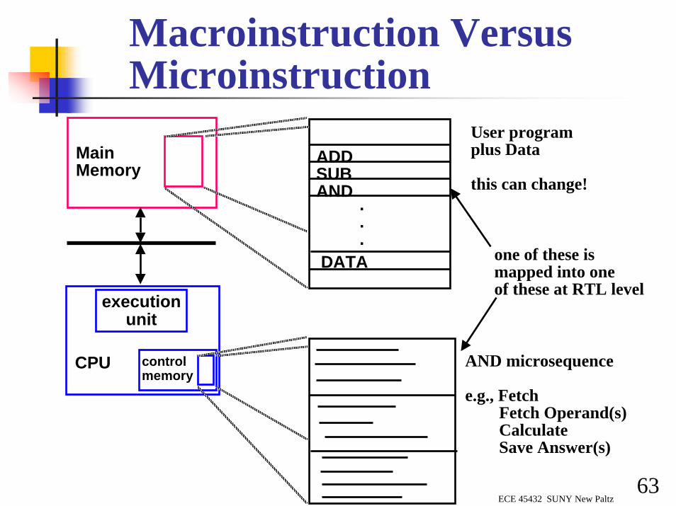
Macroinstruction Versus Microinstruction
MainMemory
executionunit
controlmemory
CPU
ADDSUBAND
DATA
.
.
.
User program plus Data
this can change!
AND microsequence
e.g., FetchFetch Operand(s)CalculateSave Answer(s)
one of these ismapped into oneof these at RTL level

ECE 45432 SUNY New Paltz64
Controller Designsequencercontrol
datapath control
micro-PCsequencer
microinstruction
The state diagrams that arise define the controller for an instruction set processor are highly structuredUse this structure to construct a simple “microsequencer” Control reduces to programming this very simple device
microprogramming
ECE 45432 SUNY New Paltz65
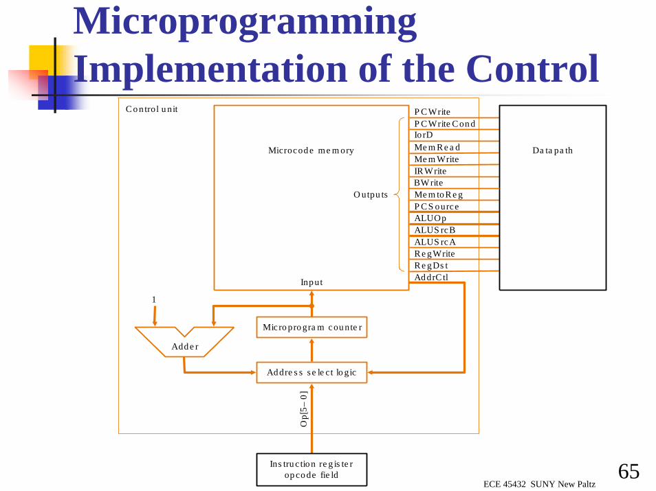
Microprogramming Implementation of the Control
P C WriteP C Write C on dIo rD
Me m toR e gP C S ourceALUOpALUS rcBALUS rcAR e gWrite
Ad drC tl
O utpu ts
Microcod e me m ory
IR Write
Me m R e a dMe m Write
R e gDs t
C o n trol u nit
Input
Mic ro pro gra m c ou nte r
Addre s s s e le ct lo gic
Op[
5–0]
Add e r
1
Da ta pa th
Ins tru c tion re g is te rop code fie ld
BWrite

ECE 45432 SUNY New Paltz66
Microprogrammingmicroinstruction: low level control instruction which defines a set of datapath control signal.A specification methodology
appropriate if hundreds of opcodes, modes, cycles, etc.signals specified symbolically using microinstructions
LabelALU
control SRC1 SRC2Register control Memory
PCWrite control Sequencing
Fetch Add PC 4 Read PC ALU SeqAdd PC Extshft Read Dispatch 1
Mem1 Add A Extend Dispatch 2LW2 Read ALU Seq
Write MDR FetchSW2 Write ALU FetchRformat1 Func code A B Seq
Write ALU FetchBEQ1 Subt A B ALUOut-cond FetchJUMP1 Jump address Fetch
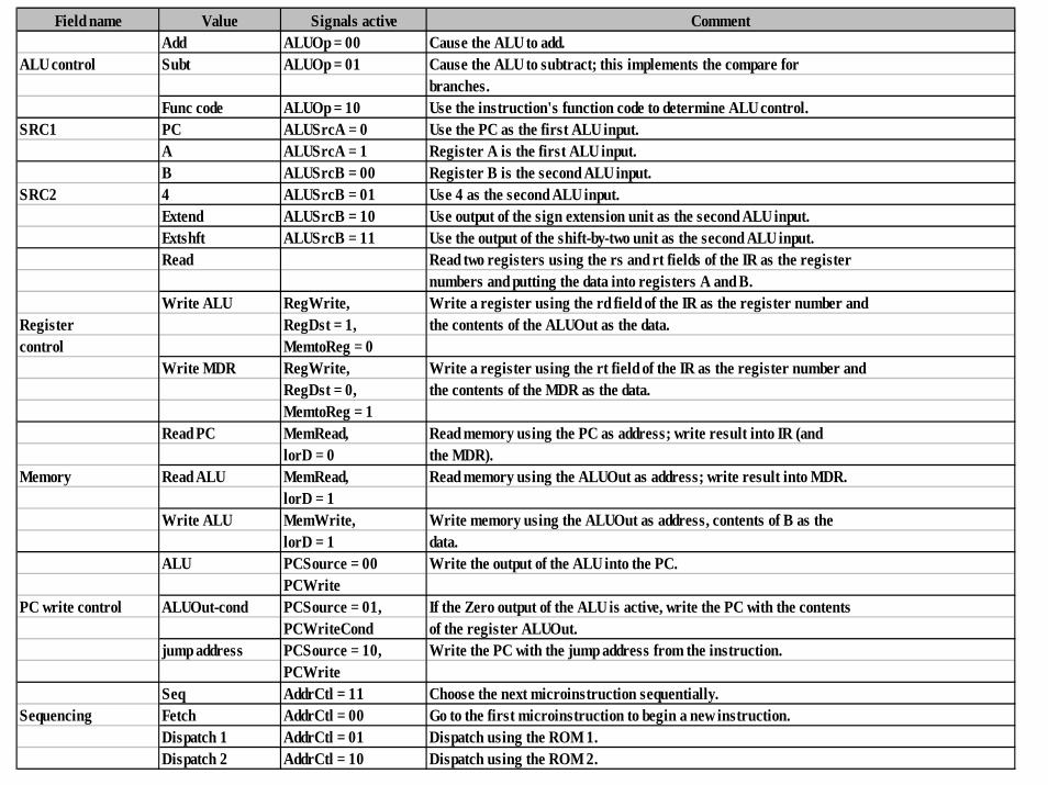
Field name Value Signals active CommentAdd ALUOp = 00 Cause the ALU to add.
ALU control Subt ALUOp = 01 Cause the ALU to subtract; this implements the compare forbranches.
Func code ALUOp = 10 Use the instruction's function code to determine ALU control.SRC1 PC ALUSrcA = 0 Use the PC as the first ALU input.
A ALUSrcA = 1 Register A is the first ALU input.B ALUSrcB = 00 Register B is the second ALU input.
SRC2 4 ALUSrcB = 01 Use 4 as the second ALU input.Extend ALUSrcB = 10 Use output of the sign extension unit as the second ALU input.Extshft ALUSrcB = 11 Use the output of the shift-by-two unit as the second ALU input.Read Read two registers using the rs and rt fields of the IR as the register
numbers and putting the data into registers A and B.Write ALU RegWrite, Write a register using the rd field of the IR as the register number and
Register RegDst = 1, the contents of the ALUOut as the data.control MemtoReg = 0
Write MDR RegWrite, Write a register using the rt field of the IR as the register number andRegDst = 0, the contents of the MDR as the data.MemtoReg = 1
Read PC MemRead, Read memory using the PC as address; write result into IR (and lorD = 0 the MDR).
Memory Read ALU MemRead, Read memory using the ALUOut as address; write result into MDR.lorD = 1
Write ALU MemWrite, Write memory using the ALUOut as address, contents of B as thelorD = 1 data.
ALU PCSource = 00 Write the output of the ALU into the PC.PCWrite
PC write control ALUOut-cond PCSource = 01, If the Zero output of the ALU is active, write the PC with the contentsPCWriteCond of the register ALUOut.
jump address PCSource = 10, Write the PC with the jump address from the instruction.PCWrite
Seq AddrCtl = 11 Choose the next microinstruction sequentially.Sequencing Fetch AddrCtl = 00 Go to the first microinstruction to begin a new instruction.
Dispatch 1 AddrCtl = 01 Dispatch using the ROM 1.Dispatch 2 AddrCtl = 10 Dispatch using the ROM 2.
ECE 45432 SUNY New Paltz68
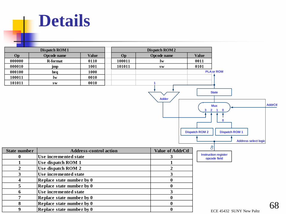
DetailsDispatch ROM 1 Dispatch ROM 2
Op Opcode name Value Op Opcode name Value000000 R-format 0110 100011 lw 0011000010 jmp 1001 101011 sw 0101000100 beq 1000100011 lw 0010101011 sw 0010
State number Address-control action Value of AddrCtl0 Use incremented state 31 Use dispatch ROM 1 12 Use dispatch ROM 2 23 Use incremented state 34 Replace state number by 0 05 Replace state number by 0 06 Use incremented state 37 Replace state number by 0 08 Replace state number by 0 09 Replace state number by 0 0
State
Adder
1
PLA or ROM
Mux3 2 1 0
Dispatch ROM 1Dispatch ROM 2
0
AddrCtl
Address select logic
Instruction registeropcode field

ECE 45432 SUNY New Paltz69
No encoding:1 bit for each datapath operationfaster, requires more memory (logic)used for Vax 780 — an astonishing 400K of memory!
Lots of encoding:send the microinstructions through logic to get control signalsuses less memory, slower
Historical context of CISC:Too much logic to put on a single chip with everything elseUse a ROM (or even RAM) to hold the microcodeIt’s easy to add new instructions
Maximally vs. Minimally Encoded
ECE 45432 SUNY New Paltz70
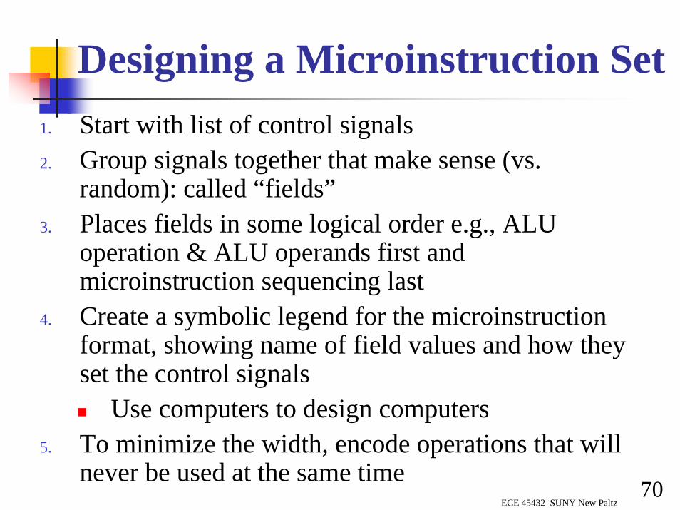
Designing a Microinstruction Set1. Start with list of control signals2. Group signals together that make sense (vs.
random): called “fields”3. Places fields in some logical order e.g., ALU
operation & ALU operands first and microinstruction sequencing last
4. Create a symbolic legend for the microinstruction format, showing name of field values and how they set the control signals
Use computers to design computers5. To minimize the width, encode operations that will
never be used at the same time
ECE 45432 SUNY New Paltz71
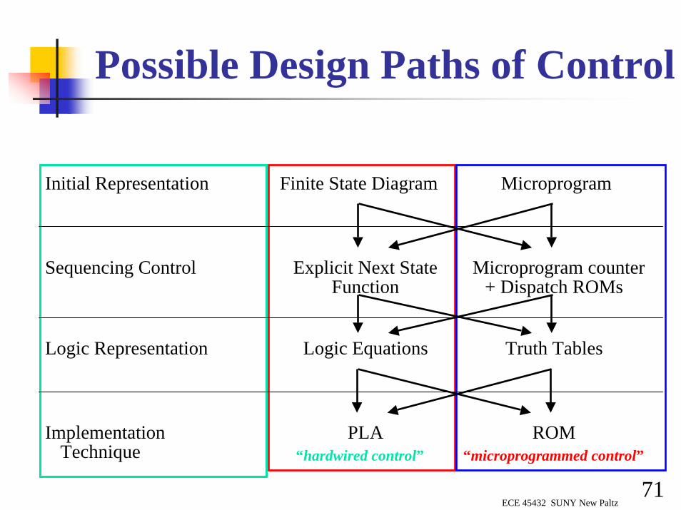
Possible Design Paths of Control
Initial Representation Finite State Diagram Microprogram
Sequencing Control Explicit Next State Microprogram counterFunction + Dispatch ROMs
Logic Representation Logic Equations Truth Tables
Implementation PLA ROM Technique “hardwired control” “microprogrammed control”

ECE 45432 SUNY New Paltz72
Microprogramming Pros and Cons
Ease of designFlexibility
Easy to adapt to changes in organization, timing, technologyCan make changes late in design cycle, or even in the field
Can implement very powerful instruction sets (just more control memory)Generality
Can implement multiple instruction sets on same machine.Can tailor instruction set to application.
CompatibilityMany organizations, same instruction set
Costly to implementSlow
ECE 45432 SUNY New Paltz73
Microcode: Trade-offsDistinction between specification and implementation is blurredSpecification Advantages:
Easy to design and write
Design architecture and microcode in parallel
Implementation (off-chip ROM) AdvantagesEasy to change since values are in memory
Can emulate other architectures
Can make use of internal registers
Implementation Disadvantages, SLOWER now that:Control is implemented on same chip as processor
ROM is no longer faster than RAM
No need to go back and make changes

ECE 45432 SUNY New Paltz74
Historical PerspectiveIn the ‘60s and ‘70s microprogramming was very important for implementing machinesThis led to more sophisticated ISAs and the VAXIn the ‘80s RISC processors based on pipelining became popularPipelining the microinstructions is also possible!Implementations of IA-32 architecture since 486
“hardwired control” for simpler instructions (few cycles, FSM control implemented using PLA or random logic)
“microcoded control” for more complex instructions(large numbers of cycles, central control store)
The IA-64 architecture uses a RISC-style ISA and can be implemented without a large central control store

ECE 45432 SUNY New Paltz75
Pentium 4
Pipelining is important (last IA-32 without it was 80386 in 1985)
Control
Control
Control
Enhancedfloating pointand multimedia
Control
I/Ointerface
Instruction cache
Integerdatapath
Datacache
Secondarycacheandmemoryinterface
Advanced pipelininghyperthreading support
Chapter 6
Chapter 7

ECE 45432 SUNY New Paltz76
Pentium 4
Somewhere in all that “control we must handle complex instructionsProcessor executes simple microinstructions, 70 bits wide (hardwired)120 control lines for integer datapath (400 for floating point)If an instruction requires more than 4 microinstructions to implement, control from microcode ROM (8000 microinstructions)Its complicated!
Control
Control
I/Ointerface
InstructioncacheData
Control
Control
Enhancedfloatingpointandmultimedia Integer
datapath
cache
Secondarycacheandmemoryinterface
Advancedpipelininghyperthreadingsupport
ECE 45432 SUNY New Paltz77
SummaryIf we understand the instructions, we can build a simple processor!
If instructions take different amounts of time, multi-cycle is better
Datapath implemented using:
Combinational logic for arithmetic logic unit
State holding elements for registers and memory
Control implemented using:
Combinational logic for single-cycle implementation
Finite state machine for multi-cycle implementation