cse140l – lab4 overall picture of lab4 tutorial on bus & memory tutorial on truth table
Post on 21-Dec-2015
224 views
TRANSCRIPT

CSE140L – Lab4
Overall picture of Lab4 Tutorial on Bus & Memory Tutorial on Truth table

CSE140L – Lab4
A simple computer system with a minimal instruction set. Load/store data Addition Shift Compare Mask

CSE140L – Lab4
System architecture
Task List You
Calculator
Marker
Pencil & Paper
Memory
(instructions)
Program
Counter
Register
Profile
DatapathControl
Logic
CLK
RST

CSE140L – Lab4
Function of each module Program counter: mark the current i
nstruction Memory: hold instructions Datapath: compute results Registers: hold data Control logic: compile instructions t
o actions.

CSE140L – Lab4
Overall picture of Lab4 A system design including register p
rofile, datapath, memory, program counter and control logic.
http://www.cse.ucsd.edu/classes/sp05/cse140L/lab/lab4/lab4.htm

CSE140L – Lab4
Tutorial on Bus & Memory Build a 16x4bit memory block Memory Elements:
(http://www.cse.ucsd.edu/classes/sp05/cse140L/lab/lab2/lib.pdf)
RAM (Writable) ROM (Read-only)
ROM16x1

CSE140L – Lab4
ROM16x1
A0A1A2A3
O
0110101100001111
INIT The data output (O) reflects the bit selected by the 4-bit address (A3 – A0). The ROM is initialized to a known value during configuration with the INIT=value parameter.

CSE140L – Lab4
16x4 memory block
addr(3:0)
data(3:0)

CSE140L – Lab4
16x4 memory block initialize
addr 1111
1110
1101
1100
1011
1010
1001
1000
0111
0110
0101
0100
0011
0010
0001
0000
INIT
data0
0 1 1 0 0 0 0 1 0 1 0 1 1 1 1 1 615F
data1
1 1 1 0 0 1 0 0 1 1 1 1 1 1 1 1 E4FF
data2
0 0 1 1 1 1 0 1 1 1 0 0 0 0 0 0 3DC0
data3
0 1 1 1 1 0 1 1 0 1 0 1 0 0 0 0 7B50

CSE140L – Lab4
Tutorial Create a project memblk Add a schematic diagram memblk to the proj
ect Create I/O markers
Menu Tools Create I/O Markers

CSE140L – Lab4
You will see two I/O buses on the canvas
Place 4 ROM16x1 modules Extend two I/O buses before
and after the ROM modulesby using “add wire” button (You will see thicker wires)

CSE140L – Lab4 Add bus taps by using “Add Bus Tap” button.
You can change the direction of by selecting the orientation in the options window.

CSE140L – Lab4 Connect the taps to module pins by wire

CSE140L – Lab4 Click on “Add Net
Name”Then type the net name in the options window.Now you will see the name appear after the cursor.
Click on the wire you want to name.

CSE140L – Lab4 Name all the nets Double click on a ROM module, the property
window will pop up. Change the INIT value and make it visible.

CSE140L – Lab4 Click OK. You will see the initial value
appears.
Change the initial values for other ROM modules and save the diagram.

CSE140L – Lab4 Create a symbol for the memory block.

CSE140L – Lab4
Tutorial on VHDL Truth Table
A2 A1 A0 D1 D0
0 0 0 0 1
0 0 1 1 1
0 1 0 1 0
0 1 1 1 0
1 0 0 1 0
1 0 1 0 1
1 1 0 1 1
1 1 1 0 0
CSE140L – Lab4
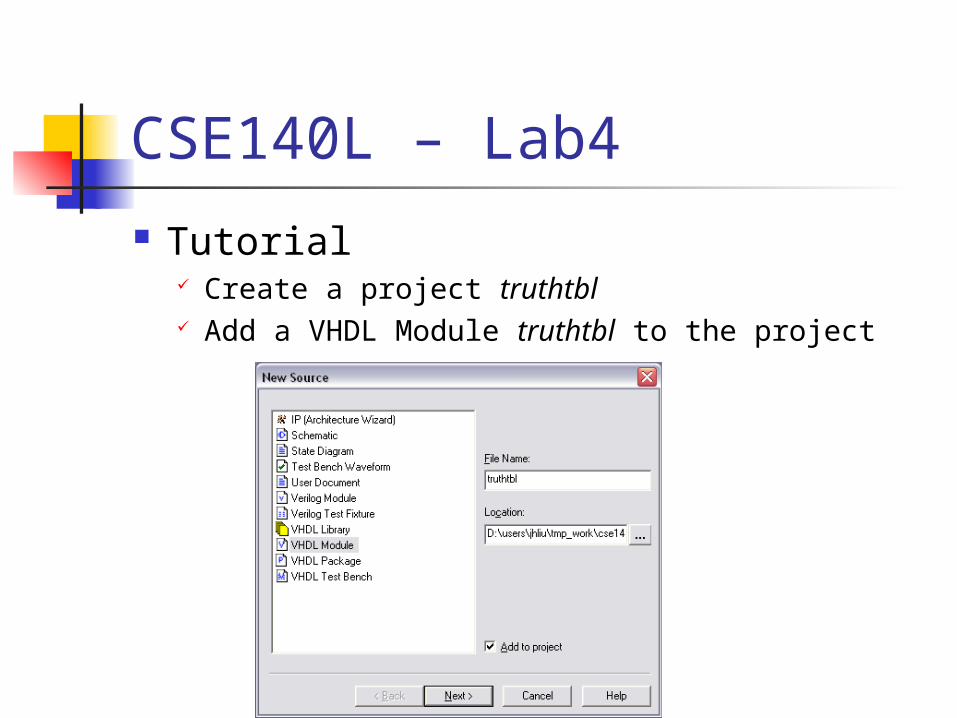
Tutorial Create a project truthtbl Add a VHDL Module truthtbl to the project

CSE140L – Lab4
You will see a template
library IEEE;use IEEE.STD_LOGIC_1164.ALL;use IEEE.STD_LOGIC_ARITH.ALL;use IEEE.STD_LOGIC_UNSIGNED.ALL;
---- Uncomment the following library declaration if instantiating---- any Xilinx primitives in this code.--library UNISIM;--use UNISIM.VComponents.all;
entity truthtbl isend truthtbl;
architecture Behavioral of truthtbl is
begin
end Behavioral;
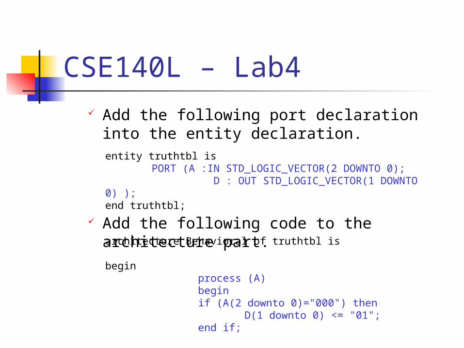
CSE140L – Lab4 Add the following port declaration into
the entity declaration.
Add the following code to the architecture part.
entity truthtbl isPORT (A :IN STD_LOGIC_VECTOR(2 DOWNTO 0); D : OUT STD_LOGIC_VECTOR(1 DOWNTO 0) );
end truthtbl;
architecture Behavioral of truthtbl is begin
process (A)beginif (A(2 downto 0)="000") then
D(1 downto 0) <= "01"; end if;

CSE140L – Lab4if (A(2 downto 0)="001") then
D(1 downto 0) <= "11"; end if;if (A(2 downto 0)="010") then
D(1 downto 0) <= "10"; end if;if (A(2 downto 0)="011") then
D(1 downto 0) <= "10"; end if;if (A(2 downto 0)="100") then
D(1 downto 0) <= "10"; end if;if (A(2 downto 0)="101") then
D(1 downto 0) <= "01"; end if;if (A(2 downto 0)="110") then
D(1 downto 0) <= "11"; end if;

CSE140L – Lab4if (A(2 downto 0)="111") then
D(1 downto 0) <= "00"; end if;
end process;
end Behavioral;
Save the VHDL file. Click on the VHDL file in the Sources
window

CSE140L – Lab4 Under the Design Utilities category in
Process View, double click on Create Schematic Symbol
Now the truth table has been implemented and can be used in top level schematic diagram.