ctemedia.s3.amazonaws.com · web viewdigital logic circuits are often referred to as logic gates....
TRANSCRIPT

CHAPTERNUMBER SYSTEMS AND
CODES

This chapter is about number systems and codes. Digital machines most frequently operate on binary, binary coded or binary related numbers. People most frequently work with decimal numbers or alphabetic characters. This alphanumeric data can be represented as binary or binary coded quantities. You will learn how to translate from one number system or code to another. This translation can be performed electronically by encoders and decoders. Of course the translation can also be done manually and several methods of accomplishing this will be outlined and demonstrated.
The material in this chapter may seem pretty abstract at first. Keep after it. It is important to learn how binary used by machines can be coded to represent a wide variety of characters. One important idea that you will see is that all true number systems presented in this chapter are constructed the same way, only the base or radix, and the character set changes.


2.1 OBJECTIVESUpon completion of this chapter you should be able to:
• Use and explain the binary number system.
• Convert from binary numbers to decimal numbers.
• Convert from decimal numbers to binary numbers.
• Use and explain the hexadecimal number system.
• Use and explain the octal number system.
• Use and explain the BCD code.
• Use and explain the ASCII code.

2.2 DISCUSSION Though you may not realize it, you are already familiar with positional number systems. The decimal system with which you have worked since grade school is a positional number system of radix or base 10. A positional number system can be constructed using any radix. Digits left of the radix point represent increasing positive powers of the radix and digits right of the radix point represent increasing negative powers of the radix. The general form of a positional number system with n digits left and right of the radix point is shown in Figure 2-1.
Notice that the constants (As) preceding the integral powers of the radix have values (weights) falling between 0 and R-l inclusive. These values or weights form the character set for the
number system. Also note that when R, the radix, is set equal to ten that the familiar decimal number system results and the radix point is called a decimal point. A positional number system like the one described here can represent R n
different integers and has a maximum integer count of R(n-1)

While any radix could be used in construction of a positional number system, digital or computer systems commonly operate on number systems of radix 2, 8, or 16. The number systems based on these three radices plus our own base 10, decimal system will be the only ones studied here. Principles learned about these number systems would apply equally well to other true positional number systems.
In addition to these true number systems, we will review special coding formats that allow us to represent decimal numbers using groups of binary bits. These are not number systems, they are codes.
Numbers will not be the only quantities represented in digital machines. Any practical system will require some method of representing alphabetic data in addition to numeric data. Several codes for representing alphanumeric data in a binary form have evolved. Examples are: the Baudot code, a five bit code named for Emile Baudot, the American Standard Code for Information Interchange (abbreviated ASCII and pronounced "as-key"), a seven bit code, and the Extended Binary-Coded-Decimal Interchange Code (abbreviated EBCDIC and pronounced "eb-see-dik"), an eight bit code. Baudot code was used in older data communication equipment such as teletypewriters. EBCDIC, developed by IBM, will normally be used in systems connected to mainframe computers. The ASCII code is the most common code used in the United States and is the only alphanumeric code covered in this text.
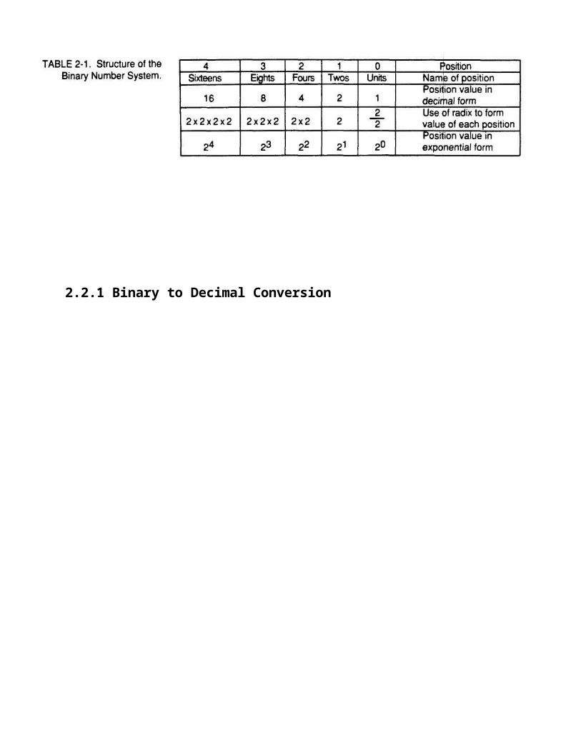
The binary number system is a positional number system with a radix of two. The binary system is the simplest useful positional number system. Each binary digit or bit can have a value of either 0 or 1. No other possibilities exist, this is the complete character set.
These two values can be represented by any device capable of distinct off and on states. The binary number system can be related to the general positional number system outlined above. Table 2-1 shows the structure of the binary number system. Notice that n bits can have 2n states and a maximum count of 2(n-1).
2.2.0 The Binary Number System

2.2.1 Binary to Decimal Conversion
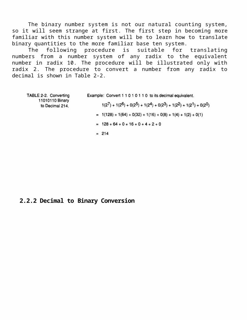
The binary number system is not our natural counting system, so it will seem strange at first. The first step in becoming more familiar with this number system will be to learn how to translate binary quantities to the more familiar base ten system.
The following procedure is suitable for translating numbers from a number system of any radix to the equivalent number in radix 10. The procedure will be illustrated only with radix 2. The procedure to convert a number from any radix to decimal is shown in Table 2-2.
2.2.2 Decimal to Binary Conversion
The procedure outline here will convert any decimal integer into it's numeric equivalent in any other radix. The procedure is:
1. Divide the given decimal integer by the radix of thenumber system to which you wish to convert.
1. Record the remainder.
2. Divide the quotient from the preceding step by the radixnumber and record any remainder.
2. Continue the process until the quotient becomes 0.

5. The remainders will form the digits of the number in the converted base. The first remainder recorded is the LSD and the last remainder recorded is the MSD. If the process of converting has been performed from left to right the number will read out in reverse order.

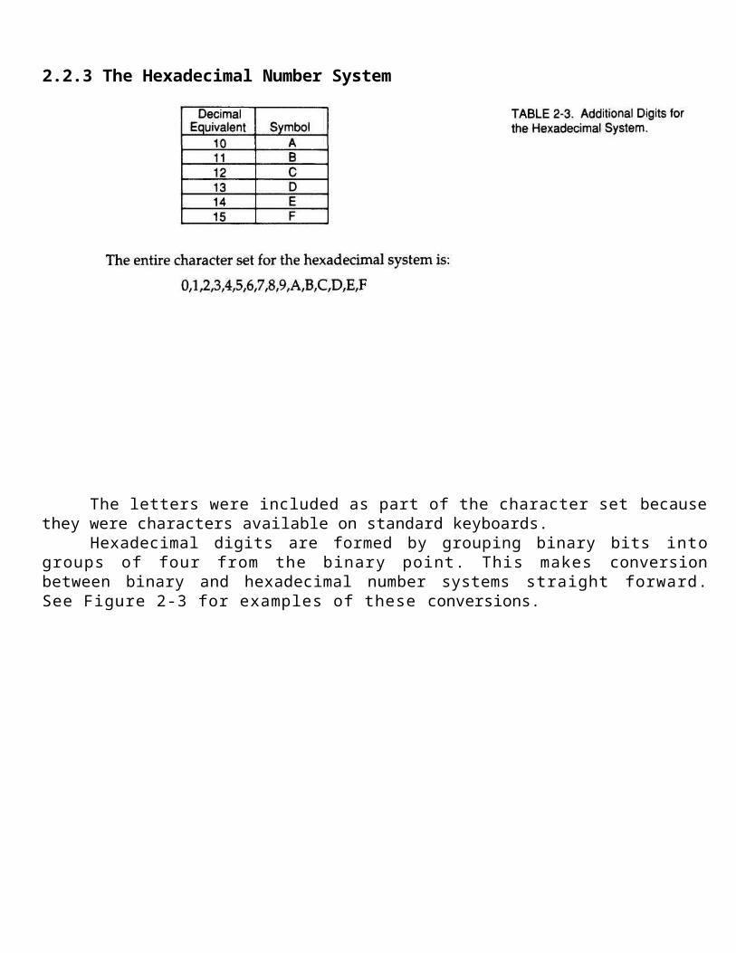
Use of binary numbers, while convenient for machines, is cumbersome to people. Any sizeable quantity expressed as a binary number has a large number of digits all of which are either 1 or 0. People are far more comfortable with shorter strings of digits with more values since that is what most of us learned in school. Also conversion from binary to decimal is cumbersome. For this reason, the hexadecimal number system (radix 16) has become widely used. The hexadecimal number system uses the same characters as the decimal system for the numbers 0-9. Table 2-3 shows the values from decimal 10 through decimal 15.

2.2.3 The Hexadecimal Number System
The letters were included as part of the character set because they were characters available on standard keyboards.
Hexadecimal digits are formed by grouping binary bits into groups of four from the binary point. This makes conversion between binary and hexadecimal number systems straight forward. See Figure 2-3 for examples of these conversions.

2.2.4 The Octal Number System

The Octal (radix 8) number system is another binary related number system. The octal number system uses the same digits for the numbers 0-7 as the decimal number system. There are no other digits in the octal character set. Octal digits are formed by evaluating binary bits in groups of three bits. The octal system is easier for humans to use than binary since the octal system uses digit characters familiar to most people. Conversion between octal and binary numbers is straight forward. See Figure 2-4 for examples of octal/binary conversions.
2.2.5 Binary Coded Decimal System

The Binary Coded Decimal (BCD) system is the first coded system studied here. A BCD number is formed by leaving a decimal number in it's normal positional notation and expressing each decimal digit using a group of four binary bits. This gives humans a means of working with a system that easily converts between decimal and binary. This also means that 6 states of the four bits are not used for coding the decimal number. Some BCD codes will use these states for error detection. Natural BCD numbers will simply code each digit of the decimal number with the four bits. Figure 2-5 illustrates this concept.

The excess-3 code is a second form of BCD code. This code avoids the all zeros and all ones states by taking the 10 values for the decimal system from the decimal equivalents of 3 to 12. A table showing binary values of the excess-3 code is shown in Table 2-4.

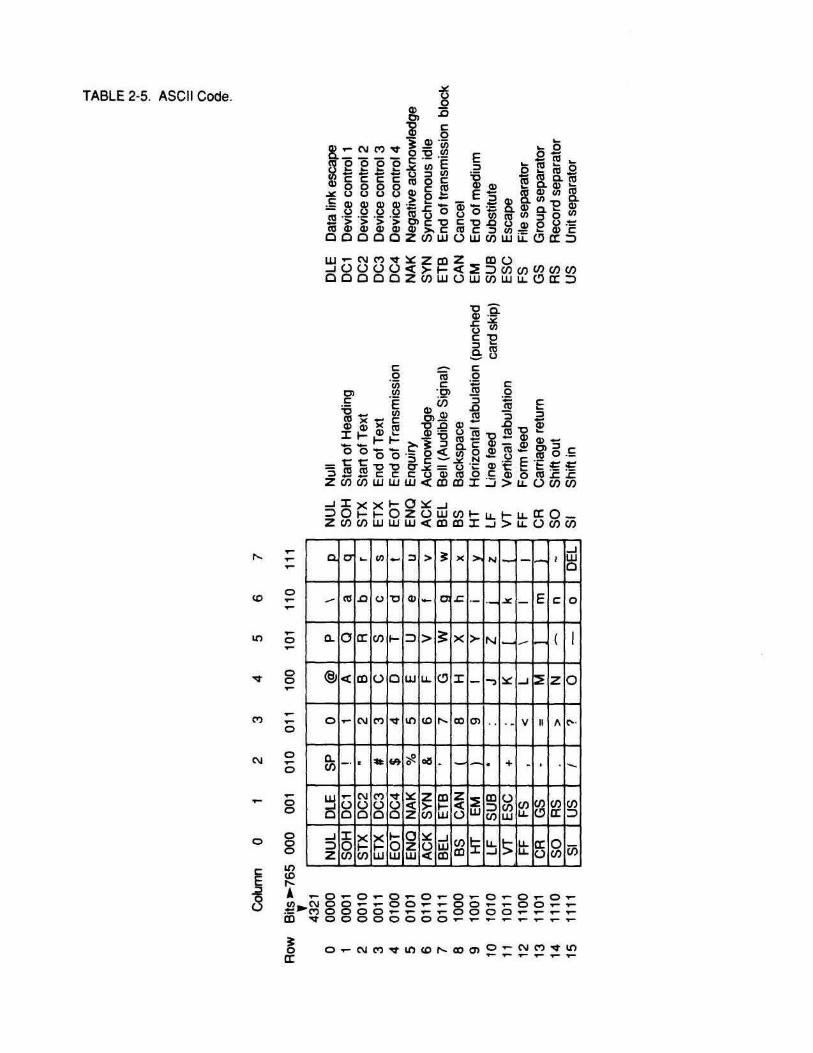
The ASCII code is the most widely used code for transfer of information in the USA. ASCII is a seven bit code which can have up to 128 values. These values are divided into three word sets. Sixty-four words are for the upper case alphabet, numbers, often used punctuation and a blank. Thirty-two words are used as machine commands. Examples of machine commands are the carriage return, line feed, and bell. The remaining thirty-two words are used for the lower case alphabet and infrequently used punctuation marks. A table of the ASCII code is shown in Table 2-5.
Some interesting consistency occurs in the ASCII code. Any upper case letter of the alphabet can be changed to lower case by changing bit 6 from 0 to 1. Also the characters which print as 0 through 9 are coded so that the lower four bits of their ASCII code is the number to be printed expressed in BCD (30 HEX to 39 HEX).

2.2.6 ASCII Code


This chapter reviewed the characteristics of number systems and codes. The number systems included were: binary, decimal, octal and hexadecimal. The codes studied were: BCD and ASCII. You were also given instructions for converting from one radix to another. When appropriate, the uses of the codes were included.
Chapters 1 and 2 have been the foundational chapters that support your future work in digital circuits. The idea that digital circuits respond to input conditions will be further developed in Chapters 3 and 4. The material covered in this chapter will gain increased importance as the study of counters, digital arithmetic circuits, are developed in Chapters 6 and 7. Take a few minutes to look over these chapters.
2.3 SUMMARY
1. What is the radix of the binary number system?
2. What is the common name for the radix ten numbersystem?
3. Which number system includes a character B ?
4. How many bits are required to represent an Octal digit?
5. What is the common name for the radix 16 numbersystem.
2.4 REVIEW QUESTIONS


6. Convert decimal 122 to binary. (Show all the steps)
7. Convert hexadecimal EF to binary.
8. Convert hexadecimal EF to decimal.
9. Air Force Work unit codes are a radix 34 system. Howmany parts can be in a system which has a three digitwork unit code?
10. Convert decimal 125 to octal.
11. Convert octal 33 to hexadecimal.
12. Convert A0 hexadecimal to decimal.
13. What binary code will be required to force an ASCIIdevice to ring the bell?
14. What is the hexadecimal value of ASCII A?
15. Convert 9 decimal to ASCII.


CHAPTERLOGIC GATES AND
BOOLEAN ALGEBRA
This chapter explores Boolean Algebra and the logic gates used to implement Boolean equations. Boolean Algebra is an area of mathematics involving operations on two-state (true-false) variables. This type of algebra was first formulated by the English Mathematician George Boole in 1854.
Boolean Algebra is based on the assumption that any proposition can be proven with correct answers to a specific number of true-false questions. Further, Boolean algebra provides a means whereby true-false logic can be handled in the form of Algebraic equations with the questions as independent variables and the conclusion expressed as a dependent variable (recall that in the equation y = A+B that A and B are independent variables and y is a dependent variable). This chapter will introduce you to the use of Boolean algebra and the use of electronic logic gates (circuits) to implement Boolean equations.
3.0 INTRODUCTION

3.1 OBJECTIVESUpon completion of this chapter you should be able to:
• Explain the basic operations of Boolean Algebra.
• Write Boolean equations.
• Use logic circuits to implement Boolean equations.

3.2 DISCUSSION
3.2.0 Boolean Variables
Boolean algebra is the branch of mathematics which studies operations on two-state variables. For the purposes of this book, an algebra is a system of mathematics where the operations of addition and multiplication can be performed with the results of the operation remaining within the system.
In Boolean algebra, addition and multiplication are the only binary (two-variable) operations which are defined. These two operations also may be performed on more than two independent variables. The only other operation in Boolean algebra is the unary (one-variable) complement function. These three operations are the only operations allowed in Boolean algebra. Mastery of these operations will be critical for understanding modern digital electronic circuitry.
Boolean variables are also known as logic state variables. Variables of this type can be in one of two possible states. The states are known as true and false. These true-false variables can be implemented with electronic devices as was illustrated in Chapter one.
Such logic devices are often described as having a 1 or 0, HI or LO, On or Off, True or False input or output. These expressions are convenient ways of noting the state of a particular Boolean variable. Keep in mind that the numbers, 1 and 0, refer to logic states and not binary integers.
Throughout the rest of this text, the terms HI, 1, and On will be used to indicate that a logical variable is True. Likewise the terms LO, 0, and Off, will indicate that the state of a logical variable is False. All exceptions to this convention will be noted.

Again, note that Boolean variables are two-state variables. Having two states allows these variables to be easily represented by electronic two-state switching circuits. Boolean variables are the basis of all modern digital electronic systems.
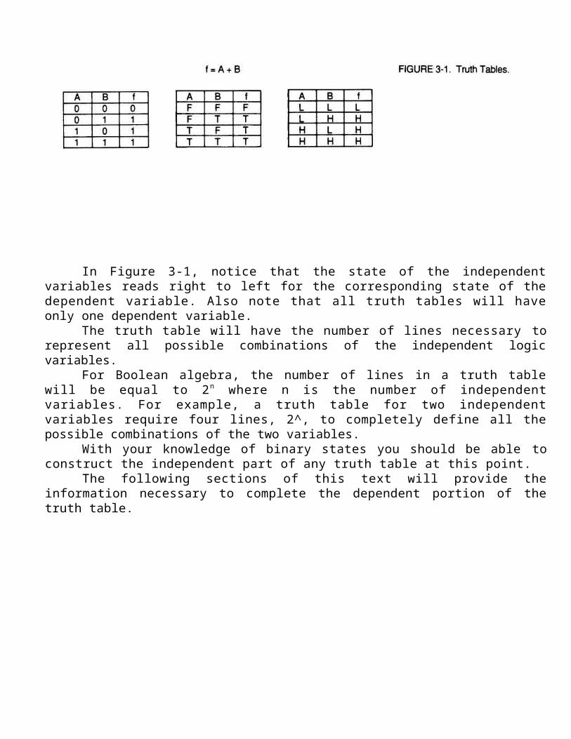
Truth tables are useful in describing relationships of Boolean variables. A truth table lists all dependent and independent variables and all possible combinations of their states. The states are listed in mnemonic form.
The independent variables are listed at the top of the truth table to the left. At the top right of the truth table is the dependent variable. Columns of the truth table show all possible states of the associated Boolean variable. Figure 3-1 shows several examples of implementing the truth table for the logical OR function.
3.2.1 Truth Tables

In Figure 3-1, notice that the state of the independent variables reads right to left for the corresponding state of the dependent variable. Also note that all truth tables will have only one dependent variable.
The truth table will have the number of lines necessary to represent all possible combinations of the independent logic variables.
For Boolean algebra, the number of lines in a truth table will be equal to 2n where n is the number of independent variables. For example, a truth table for two independent variables require four lines, 2^, to completely define all the possible combinations of the two variables.
With your knowledge of binary states you should be able to construct the independent part of any truth table at this point.
The following sections of this text will provide the information necessary to complete the dependent portion of the truth table.


3.2.2 The OR Operation
The first Boolean operation to be discussed is the logical OR operation. The OR operator operates on two or more Boolean variables. The result or dependent variable of the OR operation will be true if either one or both of the independent variables is true . The result will be false only if both of the independent variables are false. The truth table for the OR operation is shown in Figure 3-2.

3.2.3 The AND Operation
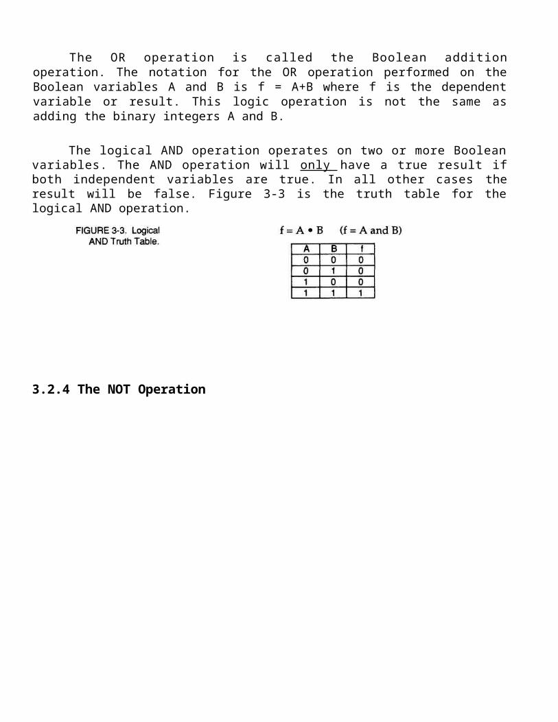
The OR operation is called the Boolean addition operation. The notation for the OR operation performed on the Boolean variables A and B is f = A+B where f is the dependent variable or result. This logic operation is not the same as adding the binary integers A and B.
The logical AND operation operates on two or more Boolean variables. The AND operation will only have a true result if both independent variables are true. In all other cases the result will be false. Figure 3-3 is the truth table for the logical AND operation.
3.2.4 The NOT Operation

The logical AND operation is called the Boolean multiplication operation. The AND operation performed on the independent variables A and B is written as f = A«B. This is not the same as multiplying binary integers.
The NOT operation is the simplest Boolean operation. It is the only unary operation allowed in Boolean algebra. This means that the operation is performed on only one Boolean independent variable or on one Boolean logic expression. The NOT function returns the complement of the state of the
Boolean variable. A truth table for the NOT operation is shown in Figure 3-4.
The NOT operation will result in the opposite logic state of the Boolean variable on which it operates. This means that TRUE Boolean variables will return a value of FALSE when operated on by the NOT operator. The NOT operator is written into Boolean equations by placing a line over the complemented variable. A~is read as "NOT A."
The AND, OR, and NOT operators are all of the basic operations in Boolean algebra. All other operations are made from these three basic operations.
Boolean equations involve combinations of these three basic functions according to the rules of Boolean algebra. Boolean algebra has its own set of rules and laws. Boolean equations are written in the same form as other mathematical equations and may involve variables and constants (1 or 0).
Many of the rules of algebra that you already are familiar with will not change in Boolean algebra. Operations in Boolean equations are performed from left to right with logic multiplication first then logic addition after products are completed. Logic equations are frequently written in the form f= A op B op C... where op signifies a logical operation (AND or OR).
Some books will use the symbol Y instead of f for the result. This is not really new to most of you as you have seen the expressions Y and f(x) used interchangeably in other algebra courses. Some common laws of Boolean algebra are listed in Table 3-1.
The Laws of Absorption can be derived from the distributive laws and the laws of tautology. As mentioned previously, the Boolean operations can be combined to solve complex problems. Logic equations are a way of describing and analyzing logical functions.

3.2.5 Logic Equations


3.2.6 Logic Circuits

When George Boole formulated Boolean algebra, electronic switching had not been invented. For lack of a suitable method of implementing logic equations, Boolean algebra was unused in technology for nearly 100 years. The invention of reliable electronic switches stimulated the use of Boolean algebra for solving logic equations.
Early switches implemented with electron tube technology could solve Boolean equations more quickly than humans but large arrays of such switches were bulky and consumed enormous amounts of electrical power. The invention of semiconductor switches was eventually responsible for the widespread use of logic circuits evident today.

Semiconductor switches have been widely used because they provide a compact, efficient, economical, and reliable method of solving logic equations. A large number of logic equations have been implemented as digital integrated circuits. These devices use several transistor switches to solve logic equations. The electrical output of these circuits represents the state of the dependent variable in the logic equation. The electrical inputs to these circuits are the states of the independent variables.
Digital logic circuits are often referred to as logic gates. The schematic symbols for the gates used to implement the basic Boolean logic equations are shown in Figure 3-5.
A logic equation can be solved by arranging logic circuits to perform the logical operations indicated by the logic equation. The electrical inputs to the circuit can be varied between the allowed states while the circuit output can be observed. This technique is used to create a truth table for the entire logic equation.
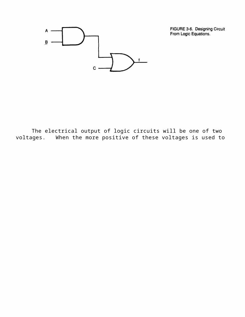
An example of converting logic equations to logic circuits is shown in Figure 3-6.
LOGIC EQUATION: Y = A • B+C
LOGIC CIRCUIT: The variables A and B must be ANDed then the result ORed with the variable C.

The electrical output of logic circuits will be one of two voltages. When the more positive of these voltages is used to


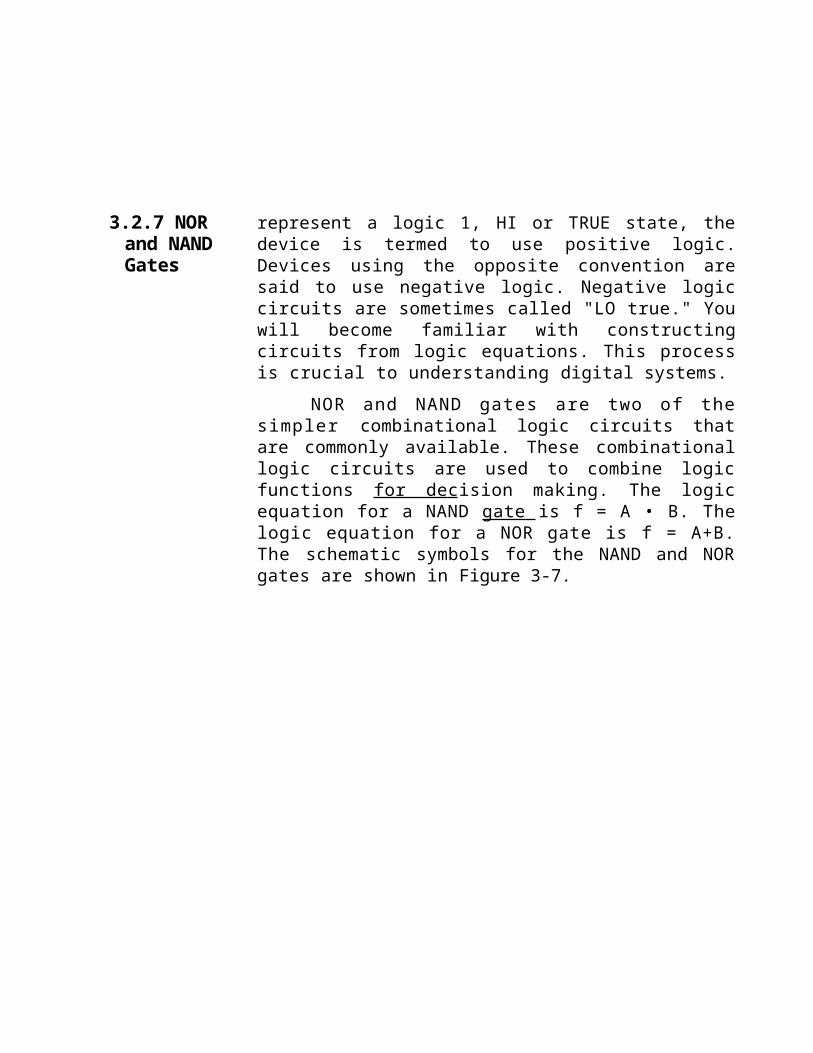
3.2.7 NOR and NAND Gates
represent a logic 1, HI or TRUE state, the device is termed to use positive logic. Devices using the opposite convention are said to use negative logic. Negative logic circuits are sometimes called "LO true." You will become familiar with constructing circuits from logic equations. This process is crucial to understanding digital systems.
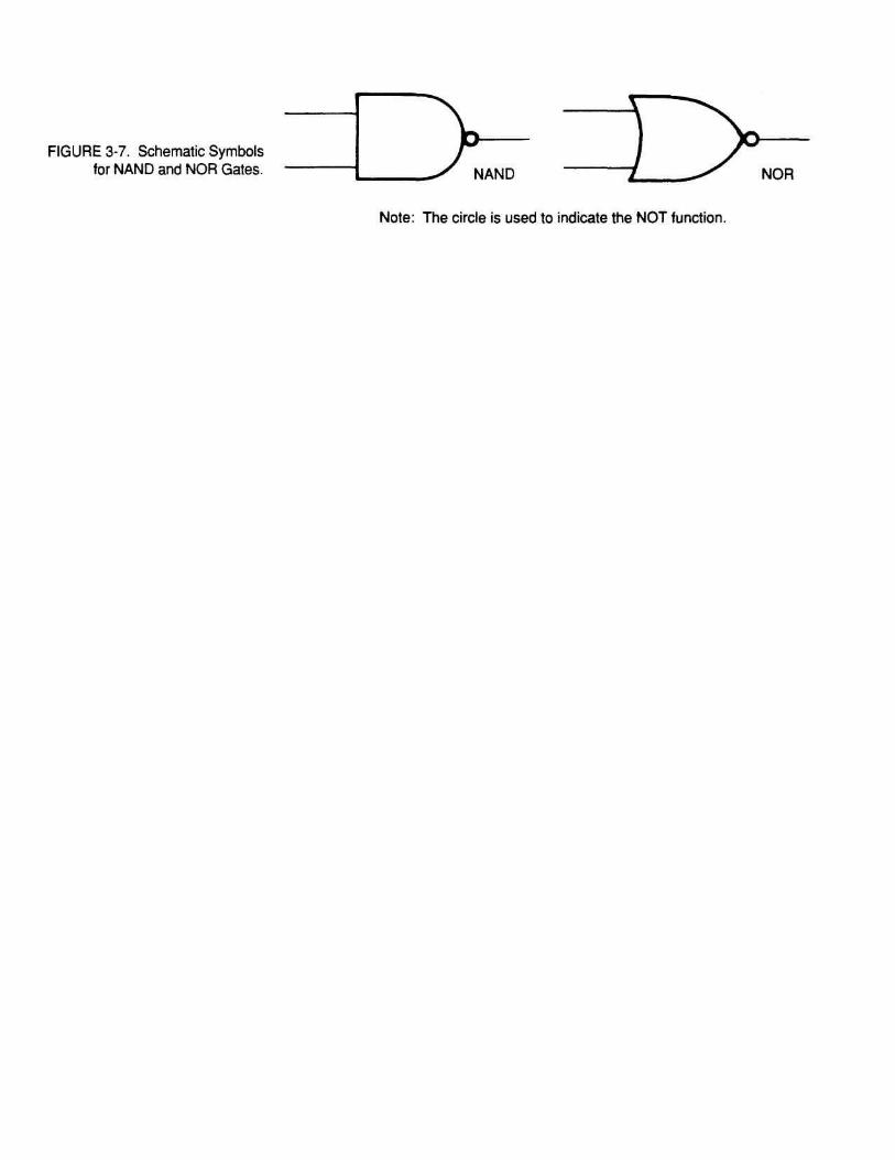
NOR and NAND gates are two of the simpler combinational logic circuits that are commonly available. These combinational logic circuits are used to combine logic functions for de cision making. The logic equation for a NAND gate is f = A • B. The logic equation for a NOR gate is f = A+B. The schematic symbols for the NAND and NOR gates are shown in Figure 3-7.

The NAND and NOR gates are the same as the AND and OR gates previously studied except that an inverter is built into the output of each circuit. Any digital circuit no matter how complex can be constructed entirely from only NAND or NOR gates. This can be readily demonstrated by implementing all the logic functions using only these gates. This fact is largely responsible for the popularity of these gates.
3.3 SUMMARY In this chapter the concepts for the use and understanding of Boolean algebra were introduced. The three basic operations used in Boolean algebra were defined and explained. The use of logic equations and some basic rules of Boolean algebra were presented.
Implementing logical equations with electronic digital circuits was explained and the schematic symbols for some common logic circuits were identified. The NOR and NAND combinational logic circuits were introduced and the flexibility of these circuits explained. The concepts learned in this chapter will be used throughout the remainder of this book and your association with digital electronics.

1. Who first formulated Boolean algebra ?
2. What is the practical use of Boolean algebra ?
3. What are the three basic operations allowed in Booleanalgebra ?
1
__________________________________________________
2
__________________________________________________
3_________________________________________________
4. How many variables does the AND function operate on?
5. How many variables does the NOT function operate on?
6. What is a truth table ?
7. Draw the truth table for the NAND function.
8. Draw the schematic symbols for the three basic logicoperations.

3.4 REVIEW QUESTIONS


9. Draw the schematic of a circuit that will perform theoperations in the following logical equation: f = C+DF.
10. Draw and complete a truth table for the equation fromquestion nine.
11. Name two of the simpler combinational logic circuits.
12. What are combinational logic circuits used for ?
13. Why have digital integrated circuits become so popular ?

LAB EXERCISE 3.1The NOT Circuit
(Inverter)
Objectives
Materials
Procedure
After completion of this experiment you will understand the operation of logic inverters (NOT gates). You will be able to use the 74LS04IC and explain its operation.
C.A.D.E.T.
74LS04 Hex Inverter
Jumper Wires
TTL Data Book
This section will begin your experiments with logic gates. You will learn some general characteristics of logic circuits then study the 74LS04 TTL hex inverter.
All logic circuits will have connections for power and ground. Logic circuits are usually seen as Dual Inline Package


Integrated Circuits known as DIP ICs. The term dual inline package describes the pin arrangement for the integrated circuit inputs and outputs.
All DIP ICs have one end or corner marked in a special way. This marking is used to show integrated circuit pin orientation. With the marked end of the IC facing away from you the pins are numbered counterclockwise from the upper left corner. Figure 3-8 shows how ICs are marked and how the pins are numbered.

The ICs used in this experiment are TTL ICs. This means the voltage of the two logic states are 0 and 5 volts. A large number of compatible integrated circuits have been manufactured as the 7400 series of TTL ICs. Correct connection of power and ground pins is crucial to circuit operation. Many 14 pin DIP ICs use pin 7 for ground and pin 14 for Vcc. Some 14 pin DIPs use pin 11 for ground and pin 4 for Vcc. Most 16 pin DIP ICs use pin 8 for ground and pin 16 for Vcc. If you connect the power and ground connections incorrectly the IC will be destroyed. For this reason, a basing diagram of all ICs used in experiments is provided. The basing diagram explains all connections to an IC and uses schematic symbols to indicate logic functions performed by the circuit. A basing diagram for the 74LS04 hex inverter is shown in Figure 3-9.


If you have trouble during the experiment, remove power from the IC and check circuit wiring. Consult with your instructor if after repeated attempts to correct the problem fail.


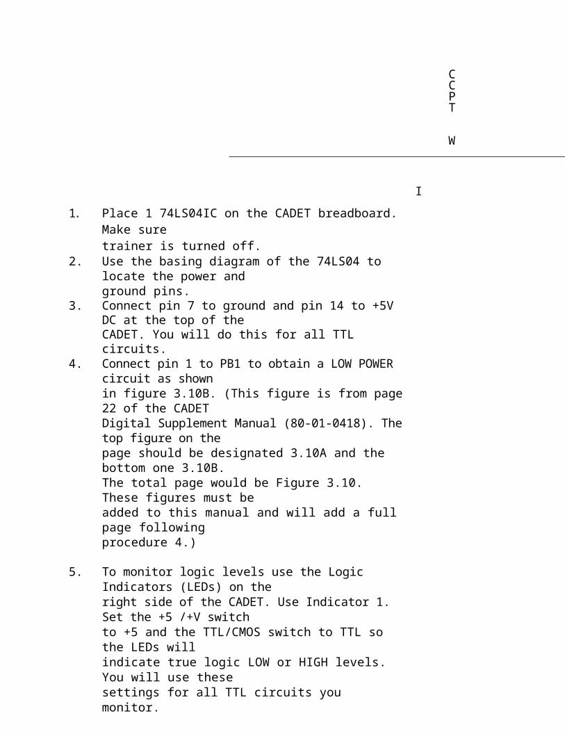
1. Place 1 74LS04IC on the CADET breadboard. Make suretrainer is turned off.
2. Use the basing diagram of the 74LS04 to locate the power andground pins.
3. Connect pin 7 to ground and pin 14 to +5V DC at the top of theCADET. You will do this for all TTL circuits.
4. Connect pin 1 to PB1 to obtain a LOW POWER circuit as shownin figure 3.10B. (This figure is from page 22 of the CADETDigital Supplement Manual (80-01-0418). The top figure on thepage should be designated 3.10A and the bottom one 3.10B.The total page would be Figure 3.10. These figures must beadded to this manual and will add a full page followingprocedure 4.)
5. To monitor logic levels use the Logic Indicators (LEDs) on theright side of the CADET. Use Indicator 1. Set the +5 /+V switchto +5 and the TTL/CMOS switch to TTL so the LEDs willindicate true logic LOW or HIGH levels. You will use thesesettings for all TTL circuits you monitor.
6. Connect pin 2 to logic indicator #2 beside your pin 1 connection. This allows monitoring the invertor output.
7. Check circuit wiring. When you are certain that the circuit iscorrectly wired, turn on the CADET power switch. Note theLEDs and record the states of Logic Indicator 1 and 2.
8. Push PB1 and record the states of Indicators 1 and 2. Note: Ahigh indicates a logic 1; low indicates logic 0.
9. Turn off power. Leave the 74LS04 IC connected until after youhave finished the following questions:
1. Construct a truth table for the 74LS04 hex invertor.2. Why is the 7404 called a hex invertor? (hint: lock at the basing
diagram).

Procedure
Questions
LAB EXERCISE 3.2 The AND GateObjectives
Materials
Book

Procedure

1. Insert the 74LS08IC into the breadboard. Make sure the traineris off.
2. Wire pin 7 to ground and pin 14 to the +5V line at the top of theCADET.
3. Wire Logic Switch 1 on the lower left of the CADET to pin 1 ofthe 74LS08 and Logic Indicator 1. This allows setting the stateof pin 1 with Logic Switch 1 and observing it's state on Indicator1.
4. Wire Logic Switch 2 to pin 2 on the 74LS08 and to Indicator 2.This allows setting and observing the state of pin 2.
5. Wire pin 3 on the 74LS08 to Logic Indicator 3. This allows observation of the AND Gate output.
6. Place Logic Switches 1 and 2 in their off state (towards thebottom of the CADET). Set the +5/+V switch above the logicswitches to +5. Set the +5/ +V switch above the logic indicatorsto +5. Turn on the CADET power switch.
7. Move Logic Switch 1 to on (up). Indicator 1 should show high.If it doesn't, check wiring to pins 1 and 2.
8. Turn switch 1 off and switch 2 on. Indicator 2 should showhigh.
9. Now use SI and S2 to determine the truth table for the 74LS08.Record your results. Observe the circuit output on indicator 3.Power down.

In this laboratory you will learn about the 74LS32 two-input OR gate.
C.A.D.E.T.
74LS32 Quad Two-input OR Gate
Jumper Wires
TTL Data Book
LAB EXERCISE 3.3 The OR GateObjectives
Materials

1. Insert the 74LS32IC into the breadboard. Make sure yourCADET is turned off and the TTL/CMOS switch is in TTLposition and the +5+V switch is in the +5 position.
2. Wire pin 7 to ground and pin 14 to +5V.3. Wire Logic Switch 1 to pin 1 on the 74LS32 and logic indicator
1. This allows setting the state of pin 1 with switch 1 andobserving its state on indicator 1.
4. Wire Logic Switch 2 to pin 2 on the 74LS32 and to indicator 2;this allows observation of the state of pin 2
5. Wire pin 3 on the 74LS32 to Indicator 3. This allows observationof the OR gate output.
6. Place Switches 1 and 2 in their off state (down)7. Make sure your +5V switch is at +5 and the TTL / CMOS switch
is set to TTL. Turn on power.8. Place Logic Switch 1 to ON. Indicators 1 and 3 should go high.9. Place Switch 1 OFF and 2 ON. Indicators 2 and 3 should show
high.10. Place Switch 2 OFF. Use the switches and indicators to deter
mine the truth table for the 74LS32. Record your observationsand then power down and remove your circuits.
Procedure


LAB EXERCISE 3.4 The NAND Gate
Objectives
Materials
In this laboratory you will learn the operation of the 74LS00 two-input NAND gate.
C.A.D.E.T.
74LSO0 Quad Two-input NAND Gate
Jumper Wires
TTL Data Book

Procedure

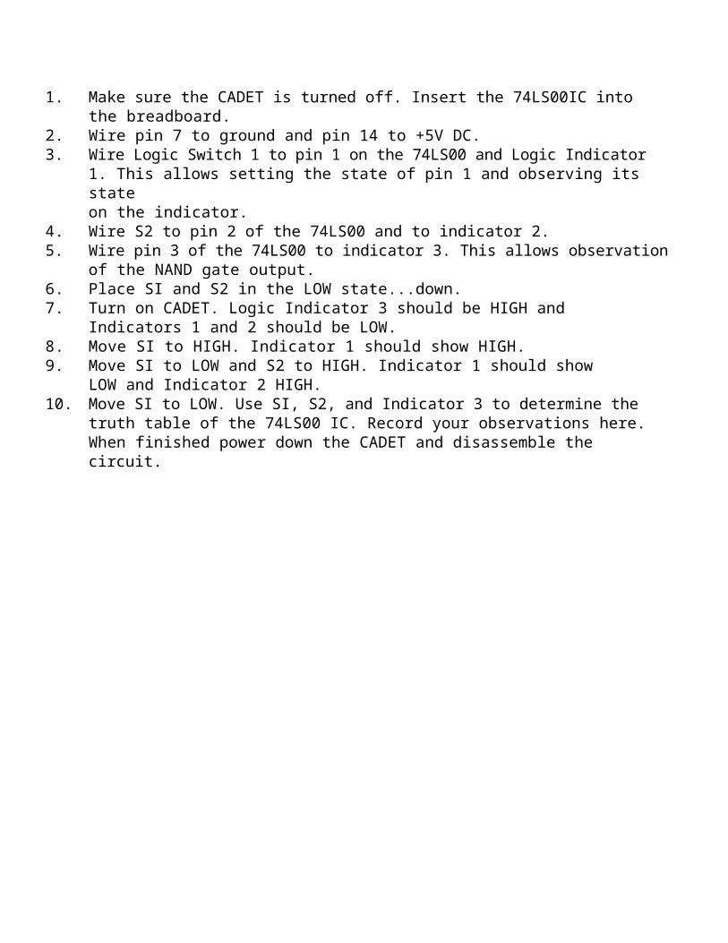
1. Make sure the CADET is turned off. Insert the 74LS00IC intothe breadboard.
2. Wire pin 7 to ground and pin 14 to +5V DC.3. Wire Logic Switch 1 to pin 1 on the 74LS00 and Logic Indicator
1. This allows setting the state of pin 1 and observing its stateon the indicator.
4. Wire S2 to pin 2 of the 74LS00 and to indicator 2.5. Wire pin 3 of the 74LS00 to indicator 3. This allows observation
of the NAND gate output.6. Place SI and S2 in the LOW state...down.7. Turn on CADET. Logic Indicator 3 should be HIGH and
Indicators 1 and 2 should be LOW.8. Move SI to HIGH. Indicator 1 should show HIGH.9. Move SI to LOW and S2 to HIGH. Indicator 1 should show
LOW and Indicator 2 HIGH.10. Move SI to LOW. Use SI, S2, and Indicator 3 to determine the
truth table of the 74LS00 IC. Record your observations here.When finished power down the CADET and disassemble thecircuit.

In this experiment you will learn the use of the 74LS02 two-input NOR gate.
C.A.D.E.T.
74LS02 Quad Two-input NOR Gate
Jumper Wires
TTL Data Book
1. Insert the 74LS02IC into the breadboard with CADET turnedoff.
1. Wire pin 7 to ground and pin 14 to +5V DC.2. Wire Indicator 1 to pin 1 of the 74LS02 to observe the state of pin
1 (NOR gate output) with Indicator 1.3. Wire S2 to pin 2 of the 74LS02 and to Indicator 2 to set and
observe the state of pin 2.4. Wire pin 3 of the 74LS02 to Indicator 3 and S3 to set and observe
the state of pin 3.2. Switch S3 and S2 in their LOW state...down.5. Turn on your CADET. Indicator 1 should be HIGH and
Indicators 2 and 3 should show LOW.6. Switch S2 to HIGH. Logic Indicator 2 should show HIGH and
Indicator 1 should go LOW.7. Switch S2 to LOW and S3 to HIGH. Indicators 1 and 2 should
show LOW, and Indicator 3 HIGH.8. Switch S3 to LOW. Use S2, S3, and Indicator 1 to determine the
truth table of the 74LS02 IC. Record your findings and thenpower down your CADET and disassemble your circuit.
LAB EXERCISE 3.5 The NOR GateObjectives Materials
Procedure
In this experiment you will confirm that NOR and NAND gates can be used to perform any logic function.
LAB EXERCISE 3.6 Using NAND and NOR GatesObjectives


Materials Procedure
C.A.D.E.T.
74LS02 Quad Two-input NOR IC
74LS00 Quad Two-input NAND IC
Jumper Wires
TTL Data Book
1. Turn off CADET and install the 74LS02 IC on the breadboard.Then wire pin 7 to ground and pin 14 to +5V.
2. Wire S2 to pin 2 and S3 to pin 3.3. Wire pin 2 to Indicator 2 and pin 3 to Indicator 3.4. Wire pin 1 to pins 5 and 6. (Shorting pins 5 and 6
causes gate2 of the quad IC to act as an invertor). Try it to convince yourselfof this.
5. Wire pin 6 to Logic Indicator 6. This is the invertor output.6. Wire pin 4 to Indicator 4. The is the invertor and
overall circuitoutput.
7. Switch S2 and S3 to LOW.8. The schematic for the circuit you have just
constructed isshown below in Figure 3-11.SEE PAGE 39 FOR FIGURE 3.11 (IT IS 3.10 IN REGULAR VERSION).
9. Turn on power to CADET. Indicator 6 should be HIGH.10. Indicators 1 and 2 monitor the state of S2 and S3.
Indicator 6monitors the NOR gate output. Indicator 4 monitors the circuitoutput. Use S2, S3, and Indicator 4 to create a truth table for thiscircuit. Record this truth table. What logic operation is this?

11. Turn your CADET off. You will now wire invertors into theinputs of the existing circuit.
12. Remove the wire at S2 and connect it to pin 10.13. Remove the wire at S3 and connect it to pin 13.14. Connect S3 to pins 11 and 12, and S2 to pins 8 and 9. The
schematic for this circuit is shown in FIGURE 3.12. FIGURE3.12 IS SHOWN ON PAGE 40 AS FIGURE 3.11.
15. Switch SI and S2 to LO. Turn on power. Use S2, S3, and LogicIndicator 4 to make a truth table for the circuit. Record your ob-servations. What logic function is performed by this circuit?
16. Use S2, S3, and Indicator 6 to make a truth table for the circuitconsisting of gates 4,3, and 1. Record your observations.Which logic function is implemented by this circuit?

17. Flip S2 and S3 HI and LO together while watching Logic Indicators 6 and 4 (output). Record your observations in the form of a truth table.


Questions 1. Which logic function is performed by the circuit observedin step 19?_________________________________________
2. All of the basic Boolean functions have beendemonstrated using the 74LS02 quad two-input NORgate. Design a circuit to implement the basic Booleanfunctions. Use the 74LS00 quad two-input NAND asyour IC. Describe which gate combinations performwhich Boolean functions. Breadboard your circuit andcheck it's operation.
