current and future capabilities of mcp detectors for uv ... · current and future capabilities of...
TRANSCRIPT
Current and future capabilities of MCP detectors for UV-Vis
instruments
John Vallerga, Oswald Siegmund, Anton Tremsin Jason McPhate
Experimental Astrophysics Group Space Sciences Laboratory
University of California, Berkeley

Microchannel Plate Detector !
Photocathode converts photon to electron
MCP(s) amplify electron by 104 to 107
Patterned anode measures charge centroid

MCP Detector Examples COS FUV for Hubble (200 x 10 mm windowless)
18 mm Optical Tube
P-Alice on New Horizons (1.1Watt, 660 gms) 200+ detector years in space
including mission to Pluto (estimated existence > 109 yrs)
The image cannot be displayed. Your computer may not have enough memory to open the image, or the image may have been corrupted. Restart your computer, and then open the file again. If the red x still appears, you may have to delete the image and then insert it again.

Advantages: •! Photon counting zero read noise •! Time tagged events < 100 ps •! Large, flexible format > 100 mm
(0.1Gpxl)
•! High dynamic range 108
•! Spatial resolution < 15 mm FWHM •! Low out of band response •! Ability to smoothly curve focal plane •! Room temperature operation •! Robust and reliable •! Radiation hard

Disadvantages: •! QE dependent on photocathode •! Fixed pattern noise •! Spatial non-linearity •! Low throughput •! Lifetime (~ 3 Coulombs cm-2) •! High Voltage operation •! Vacuum operation (pumps, doors, vacuum
tubes)
MCP fabrication
Better anode Faster electronics
Lower gain (x10-100) Lower gain – Lower HV
Solutions
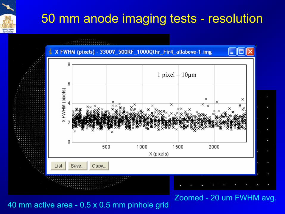
Zoomed - 20 um FWHM avg.
50 mm anode imaging tests - resolution
40 mm active area - 0.5 x 0.5 mm pinhole grid
1 pixel = 10!m
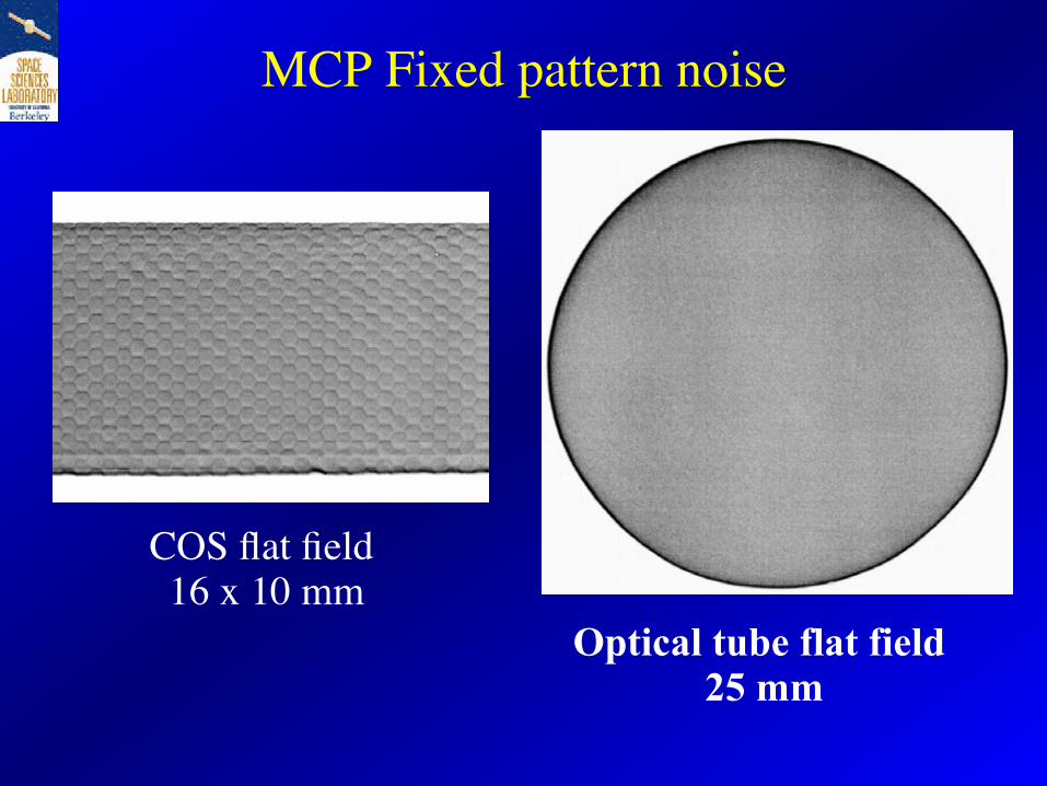
MCP Fixed pattern noise!
COS flat field !16 x 10 mm!
Optical tube flat field 25 mm

Photocathodes, 10nm - 900nm!
General comparison of conventional and GaN photocathodes.
GaN is a robust material with good handling properties. Samples have been re-cleaned and reprocessed many times achieving same QE GaN sample in a sealed tube has not changed in QE measurably in over 5.5 years.
1
10
100
100 1000
SuperGen2GaAsGaN-b12GaAsPCsTeCsIKBrQ
uant
um D
etec
tion
Effic
ienc
y (%
)
Wavelength (nm)
Recent improvements in bialkali cathodes, fills the gap between GaN and GaAsP. PHOTONIS – Clermont-Ferrand workshop 2010

Borosilicate glass MCPs!
Fabricated using hollow tube draw and stack technique
Glass is inexpensive, low Z (no lead), and has a higher softening temperature
- Lower gamma background
- Deposition of high T opaque photocathodes like GaN
Functionalized using Atomic Layer Deposition (ALD) - Semiconductor Resistive layer, tunable over wide range
- Amplifying layer (Al2O3) with high secondary electron coeff.
- Better lattice match to GaN
Separates surface optimization from substrate optimization!

Micro-capillary arrays (Incom) with 20 !m or 40!m pores (8° bias) made with borosilicate glass. L/d typically 60:1 but can be much larger. Open area ratios from 60% to 83%. These are made with hollow tubes, no etching is needed.
Borosilicate Microchannel Plate Substrates
20 !m pore borosilicate micro-capillary substrate. Pore distortions at multifiber boundaries, otherwise very uniform.
40 !m pore borosilicate micro-capillary substrate with 83% open area
Coming soon, 10 !m pore borosilicate micro-capillary substrate with 50% open area
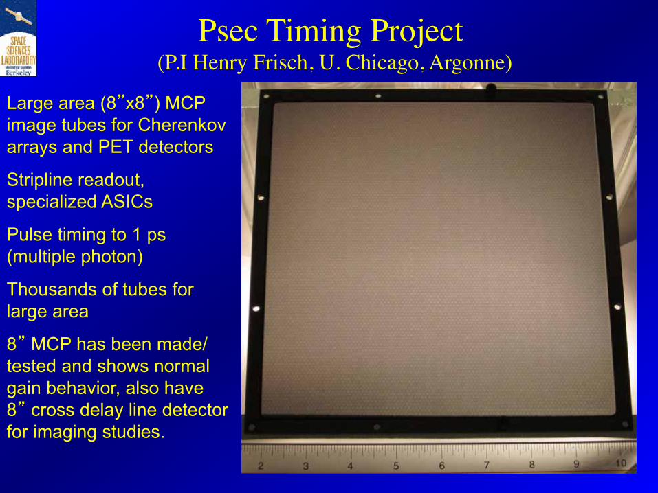
Psec Timing Project "(P.I Henry Frisch, U. Chicago, Argonne)!
Large area (8 x8 ) MCP image tubes for Cherenkov arrays and PET detectors
Stripline readout, specialized ASICs
Pulse timing to 1 ps (multiple photon)
Thousands of tubes for large area
8 MCP has been made/tested and shows normal gain behavior, also have 8 cross delay line detector for imaging studies.
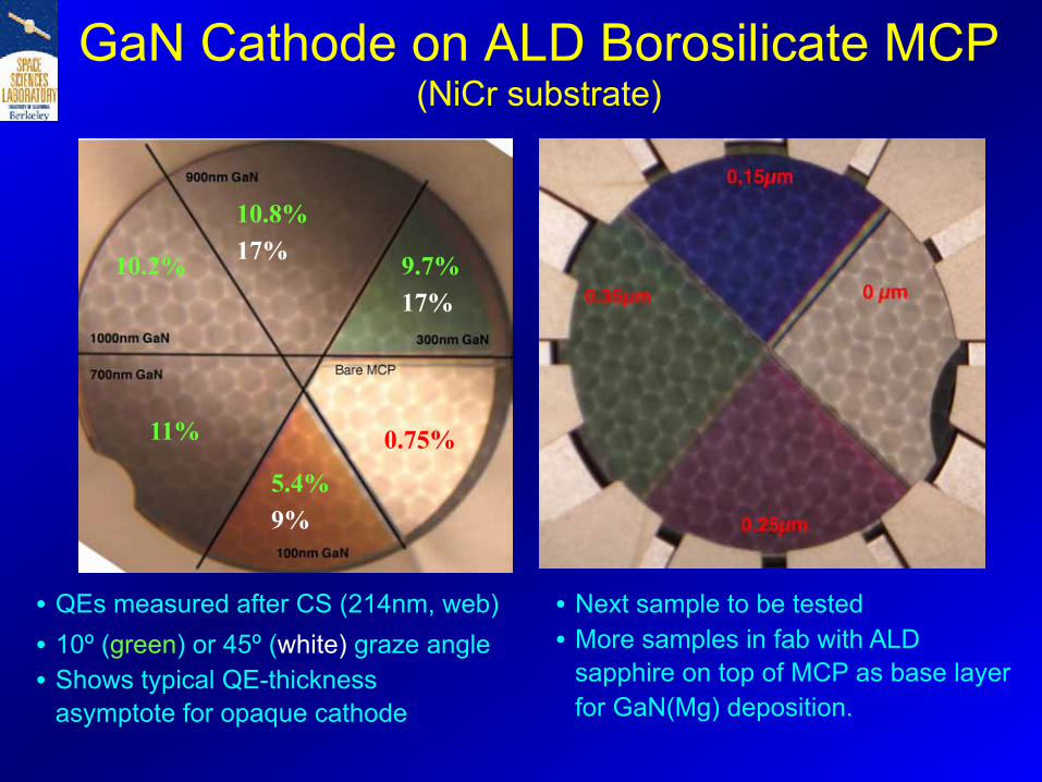
•! QEs measured after CS (214nm, web) •! 10º (green) or 45º (white) graze angle •! Shows typical QE-thickness
asymptote for opaque cathode
GaN Cathode on ALD Borosilicate MCP (NiCr substrate)!
0.75%
9.7% 17%
5.4% 9%
11%
10.8% 17% 10.2%
•! Next sample to be tested •! More samples in fab with ALD
sapphire on top of MCP as base layer for GaN(Mg) deposition.

MCP detector performance 1985 2011 2020
Pixel Size (µm) 50 5 5
Format (mm) 100 100 200
Global Ct. rate (kHz) 5 4,000 40,000
Local Ct. rate (kHz) 1 40 40
Dark rate (cts cm-2 s-1) 0.5 .085 .085
Pixels (Mpixel) 0.7 64 1600
MCP Detectors have been the workhorse in UV imaging for decades Most of the order-of-magnitude improvements (e.g. throughput, resolution) have been due to advances in microelectronics which are now being implemented for flight programs New ALD coating technologies have resulted in a very rapid development of Borosilicate MCPs that can be larger, quieter, and survive higher temperatures that facilitate new photocathode deposition techniques (e.g. opaque GaN) Clearly there is still work to do:
Improve QE in all bands Demonstrate stability and low background with each improvement Scaling readouts to the largest formats Raise TRL level of each new technology
MCP Sensor Progress & Prospects
Acknowledgements:- Mr. J. Hull,, and Mr. R. Raffanti. This work was supported by NASA under Grants NNX09AF73G and NNX08AE04G.