current fed multipulse rectifier approach for …eprints.nottingham.ac.uk/52950/1/current fed...
TRANSCRIPT

0885-8993 (c) 2018 IEEE. Personal use is permitted, but republication/redistribution requires IEEE permission. See http://www.ieee.org/publications_standards/publications/rights/index.html for more information.
This article has been accepted for publication in a future issue of this journal, but has not been fully edited. Content may change prior to final publication. Citation information: DOI 10.1109/TPEL.2018.2849927, IEEETransactions on Power Electronics
Current Fed Multipulse Rectifier Approach forUnidirectional HVDC and MVDC Applications
Gustavo Lambert, Student Member, IEEE, Marcus V. Soares, Student Member, IEEE,Pat Wheeler, Senior Member, IEEE, Marcelo L. Heldwein, Senior Member, IEEE,
and Yales R. de Novaes, Member, IEEE
Abstract—Even though multipulse rectifiers are a long es-tablished and well-known technology, still their behavior isnot fully described in the literature when they are fed bythree-phase balanced sinusoidal currents sources. To addressthe aforementioned gap, this work presents the operation andproperties of current-fed multipulse rectifiers. The undertakenaim is achieved by analyzing the examined topology throughcircuit analysis and then, the theoretical results are validatedthrough comparisons with the simulated waveforms and experi-mental results. Furthermore, the expected harmonic content andthe duality with traditional voltage-fed multipulse rectifiers arepresented. In the proposed structure, the transformer voltagespresent a multipulse waveform, instead of its primary currentsas in voltage-fed multipulse rectifiers. This implies on limitingthe voltage steps and its derivative which might be beneficial toreduce cost and volume of insulation, particularly for MVDCand HVDC applications. Besides that, by actively controlling theprimary currents, a possible copper loss reduction is shown inthe transformer windings, differentiating the proposed structurefrom its voltage controlled counterpart.
Index Terms—Multipulse Rectifier, DC-DC, Medium Fre-quency, Current Source.
I. INTRODUCTION
H IGH-POWER dc-dc converters play an important roleenabling the emergent dc grid proposition to have many
applications such as electric railways [1], [2], HVDC systems[3], [4], renewable generation [5], [6], all-electric ships [7],dc multi-terminal interconnection [8] and others all of whichrequire a medium or high voltage dc interface. The use ofdc offers some advantages over traditional ac links suchas the lower conduction losses, the asynchronous operation,the higher active power transfer capability and the absenceof low-frequency reactive energy circulation. However, theseadvantages lead to economically viable solutions typically forlong distance scenarios or non-standard applications.
Among the cited applications, this paper particularly aimsto address the ones with unidirectional power flow through thedevelopment of an isolated dc-dc converter for medium or highvoltage dc interfaces. In particular, the proposed solution mightbe advantageously deployed in future subsea transmission anddistribution system applied to oil and gas extraction [9], [10]which requires the converter to be: compatible with medium orhigh voltage, limited in volume and weight, and galvanicallyisolated.
For the first requirement, compatibility with medium/highvoltage, the main options that have been presented in theliterature are based on the Dual Active Bridge (DAB) [11],
[12] or based on the Modular Multilevel Converter (MMC)[13], [14]. However, the high dv/dt and the high voltage stepsapplied in medium/high frequency transformers [15] are stillan issue because of their interaction with transformer parasiticelements that may cause two principal effects. The first iscurrent spikes due to capacitive coupling discharges and thesecond is overvoltages that are caused by leakage inductances[16]. Both interactions are problematic for the converter andmay cause malfunction or even its failure.
Subsea engineering applications typically have restrictionswith volume and weight, the second requirement. Thus, oneknown approach is to increase the frequency in the ac stages toreduce the dimensions of the converter. This frequency maybe increased from hundreds of hertz up to tens of kilohertzbefore the losses became problematic. The choice offers anoptimization design challenge due to commercially availablemagnetic material and thermal restrictions [17].
The galvanic isolation between input(s) and output(s) termi-nals is the last requirement. It is important from the operationpoint of view because it allows the connection of differentsource or load references (series or parallel). In addition, itenables the fault isolation capability which, for example, isextremely important to avoid the shutdown of large gas andoil production plant [18].
Although a wide variety of isolated converters are pro-posed, which make use of single-phase transformers (mostlyexpandable to a three-phase configuration), few are proposedusing the Multipulse Rectifier (MR) concept [19]. This type ofrectifier has long been presented and can be found typicallyfrom 12 to 36 pulses in multiples of 6 [20]–[22]. Its maincharacteristics are the reduction of reactive energy circulationthrough harmonic cancellation and the higher frequency rippleat the output.
As a solution for the aforementioned requirements, acurrent-fed MR is proposed. This converter was previouslypresented as part of the two-stage step-down dc-dc converter(hundreds of kV to tens of kV) shown in Fig. 1 [10]. Inthis paper, the focus is to further analyze the properties andparticularities of the MR fed by three-phase balanced currentsources. This is achieved through theoretical analysis of thecircuit and verification of simulated waveforms to illustratethe converter behavior. Further than its operation, the paperalso addresses the harmonics cancellation and distribution, theduality with traditional voltage-fed MR and the current stresson its diodes. Since the MR is a wide class of ac-dc converters,this paper chooses to focus on the 12-pulse series-type diode
0885-8993 (c) 2018 IEEE. Personal use is permitted, but republication/redistribution requires IEEE permission. See http://www.ieee.org/publications_standards/publications/rights/index.html for more information.
This article has been accepted for publication in a future issue of this journal, but has not been fully edited. Content may change prior to final publication. Citation information: DOI 10.1109/TPEL.2018.2849927, IEEETransactions on Power Electronics
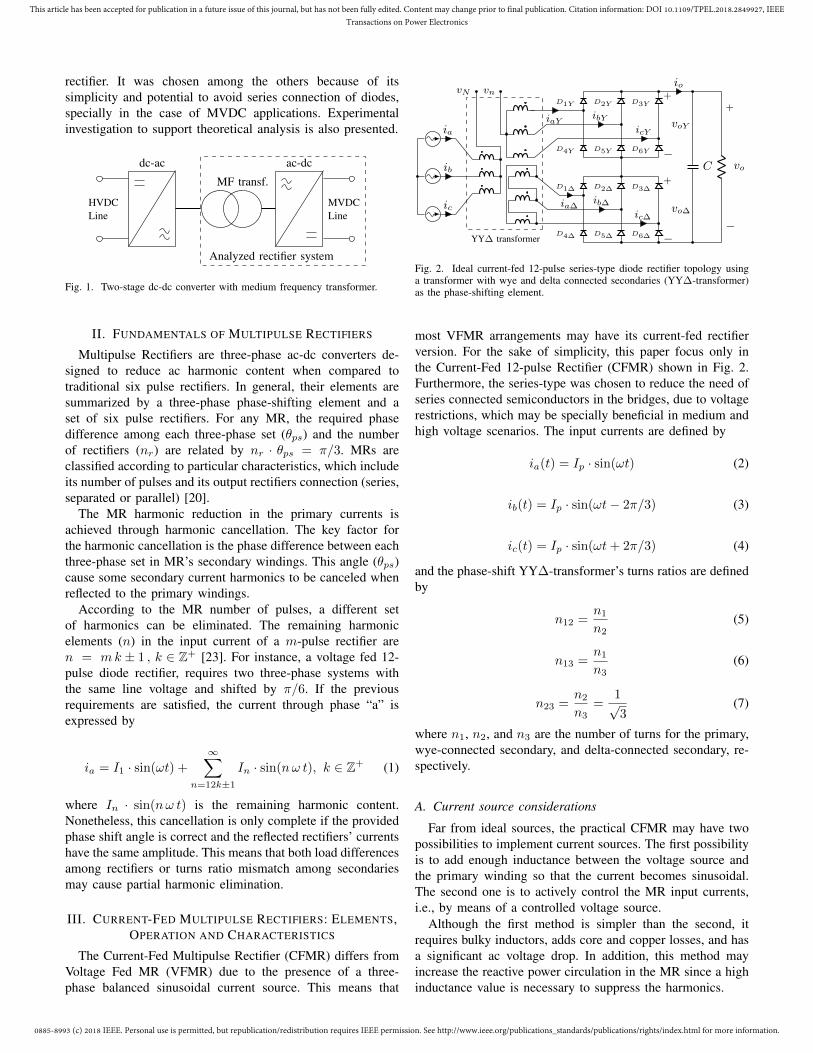
rectifier. It was chosen among the others because of itssimplicity and potential to avoid series connection of diodes,specially in the case of MVDC applications. Experimentalinvestigation to support theoretical analysis is also presented.
dc-ac
MF transf.
ac-dc
HVDCLine
MVDCLine
Analyzed rectifier system
Fig. 1. Two-stage dc-dc converter with medium frequency transformer.
II. FUNDAMENTALS OF MULTIPULSE RECTIFIERS
Multipulse Rectifiers are three-phase ac-dc converters de-signed to reduce ac harmonic content when compared totraditional six pulse rectifiers. In general, their elements aresummarized by a three-phase phase-shifting element and aset of six pulse rectifiers. For any MR, the required phasedifference among each three-phase set (θps) and the numberof rectifiers (nr) are related by nr · θps = π/3. MRs areclassified according to particular characteristics, which includeits number of pulses and its output rectifiers connection (series,separated or parallel) [20].
The MR harmonic reduction in the primary currents isachieved through harmonic cancellation. The key factor forthe harmonic cancellation is the phase difference between eachthree-phase set in MR’s secondary windings. This angle (θps)cause some secondary current harmonics to be canceled whenreflected to the primary windings.
According to the MR number of pulses, a different setof harmonics can be eliminated. The remaining harmonicelements (n) in the input current of a m-pulse rectifier aren = mk ± 1 , k ∈ Z+ [23]. For instance, a voltage fed 12-pulse diode rectifier, requires two three-phase systems withthe same line voltage and shifted by π/6. If the previousrequirements are satisfied, the current through phase “a” isexpressed by
ia = I1 · sin(ωt) +∞∑
n=12k±1
In · sin(nω t), k ∈ Z+ (1)
where In · sin(nω t) is the remaining harmonic content.Nonetheless, this cancellation is only complete if the providedphase shift angle is correct and the reflected rectifiers’ currentshave the same amplitude. This means that both load differencesamong rectifiers or turns ratio mismatch among secondariesmay cause partial harmonic elimination.
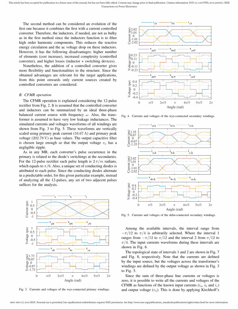
III. CURRENT-FED MULTIPULSE RECTIFIERS: ELEMENTS,OPERATION AND CHARACTERISTICS
The Current-Fed Multipulse Rectifier (CFMR) differs fromVoltage Fed MR (VFMR) due to the presence of a three-phase balanced sinusoidal current source. This means that
ic
ib
ia
D4∆
D1∆
D4Y
D1Y
D5∆
D2∆
D5Y
D2Y
D6∆
D3∆
D6Y
D3Y+
−
voY
+
−
vo∆
io
C
iaY ibYicY
ia∆ib∆
ic∆
+
−
vo
vN vn
YY∆ transformer
Fig. 2. Ideal current-fed 12-pulse series-type diode rectifier topology usinga transformer with wye and delta connected secondaries (YY∆-transformer)as the phase-shifting element.
most VFMR arrangements may have its current-fed rectifierversion. For the sake of simplicity, this paper focus only inthe Current-Fed 12-pulse Rectifier (CFMR) shown in Fig. 2.Furthermore, the series-type was chosen to reduce the need ofseries connected semiconductors in the bridges, due to voltagerestrictions, which may be specially beneficial in medium andhigh voltage scenarios. The input currents are defined by
ia(t) = Ip · sin(ωt) (2)
ib(t) = Ip · sin(ωt− 2π/3) (3)
ic(t) = Ip · sin(ωt+ 2π/3) (4)
and the phase-shift YY∆-transformer’s turns ratios are definedby
n12 =n1
n2(5)
n13 =n1
n3(6)
n23 =n2
n3=
1√3
(7)
where n1, n2, and n3 are the number of turns for the primary,wye-connected secondary, and delta-connected secondary, re-spectively.
A. Current source considerations
Far from ideal sources, the practical CFMR may have twopossibilities to implement current sources. The first possibilityis to add enough inductance between the voltage source andthe primary winding so that the current becomes sinusoidal.The second one is to actively control the MR input currents,i.e., by means of a controlled voltage source.
Although the first method is simpler than the second, itrequires bulky inductors, adds core and copper losses, and hasa significant ac voltage drop. In addition, this method mayincrease the reactive power circulation in the MR since a highinductance value is necessary to suppress the harmonics.
0885-8993 (c) 2018 IEEE. Personal use is permitted, but republication/redistribution requires IEEE permission. See http://www.ieee.org/publications_standards/publications/rights/index.html for more information.
This article has been accepted for publication in a future issue of this journal, but has not been fully edited. Content may change prior to final publication. Citation information: DOI 10.1109/TPEL.2018.2849927, IEEETransactions on Power Electronics
The second method can be considered an evolution of thefirst one because it combines the first with a current controlledconverter. Therefore, the inductors, if needed, are not as bulkyas in the first method since the inductors function is to filterhigh order harmonic components. This reduces the reactiveenergy circulation and the ac voltage drop on these inductors.However, it has the following disadvantages: higher numberof elements (cost increase), increased complexity (controlledconverter), and higher losses (inductor + switching devices).
Nonetheless, the addition of a controlled converter givesmore flexibility and functionalities to the structure. Since theobtained advantages are relevant for the target applications,from this point onwards only current sources created bycontrolled converters are considered.
B. CFMR operation
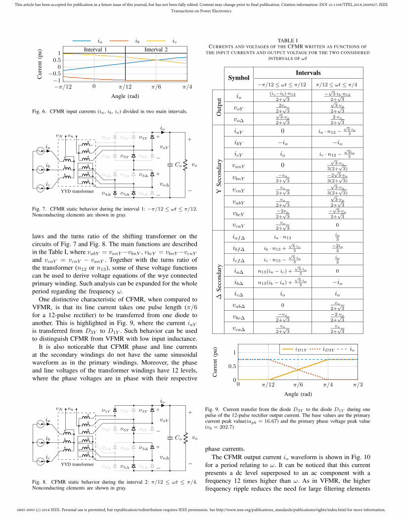
The CFMR operation is explained considering the 12-pulserectifier from Fig. 2. It is assumed that the controlled converterand inductors can be summarized by an ideal three-phasebalanced current source with frequency ω. Also, the trans-former is assumed to have very low leakage inductances. Thesimulated currents and voltages waveforms of all windings areshown from Fig. 3 to Fig. 5. These waveforms are verticallyscaled using primary peak current (16.67 A) and primary peakvoltage (202.78 V) as base values. The output capacitive filteris chosen large enough so that the output voltage vo has anegligible ripple.
As in any MR, each converter’s pulse occurrence in theprimary is related to the diode’s switchings at the secondaries.For the 12-pulse rectifier each pulse length is 2π/m radians,which equals to π/6. Also, a unique set of conducting diodes isattributed to each pulse. Since the conducting diodes alternatein a predictable order, for this given particular example, insteadof analyzing all the 12-pulses, any set of two adjacent pulsessuffices for the analysis.
-1 -0.50
0.5 1
Cu
rren
t (p
u)
ia
ib
ic
-1
-0.5
0
0.5
1
Vo
ltag
e (p
u)
vaN
vbN
vcN
0 /3 2 /3 4 /3 5 /3 2
Angle (rad)
-1.73-0.87
0 0.87 1.73
Vo
ltag
e (p
u)
vab
vbc
vca
Fig. 3. Currents and voltages of the wye-connected primary windings.
-2.02-1.01
0 1.01 2.02
Cu
rren
t (p
u)
iaY
ibY
icY
-0.23-0.11
0 0.11 0.23
Vo
ltag
e (p
u)
vanY
vbnY
vcnY
0 /3 2 /3 4 /3 5 /3 2
Angle (rad)
-0.4
-0.2
0
0.2
0.4
Vo
ltag
e (p
u)
vabY
vbcY
vcaY
Fig. 4. Currents and voltages of the wye-connected secondary windings.
-1.35-0.67
0 0.67 1.35
Cu
rren
t (p
u)
iaf
ibf
icf
-2.02-1.01
0 1.01 2.02
Cu
rren
t (p
u)
ia
ib
ic
0 /3 2 /3 4 /3 5 /3 2
Angle (rad)
-0.4-0.20
0.2 0.4
Vo
ltag
e (p
u)
vab
vbc
vca
Fig. 5. Currents and voltages of the delta-connected secondary windings.
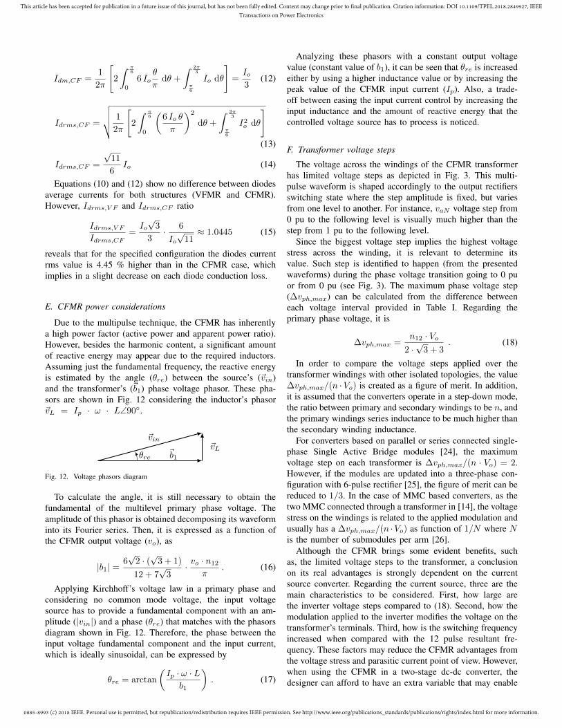
Among the available intervals, the interval range from−π/12 to π/4 is arbitrarily selected. Where the interval 1ranges from −π/12 to π/12 and the interval 2 from π/12 toπ/4. The input currents waveforms during these intervals areshown in Fig. 6.
The topological state of intervals 1 and 2 are shown in Fig. 7and Fig. 8, respectively. Note that the currents are definedby the input source, but the voltages across the transformer’swindings are defined by the output voltage as shown in Fig. 3to Fig. 5.
Since the sum of three-phase line currents or voltages iszero, it is possible to write all the currents and voltages of theCFMR as functions of the known input currents (ia, ib and ic)and output voltage (vo). This is done by applying Kirchhoff’s
0885-8993 (c) 2018 IEEE. Personal use is permitted, but republication/redistribution requires IEEE permission. See http://www.ieee.org/publications_standards/publications/rights/index.html for more information.
This article has been accepted for publication in a future issue of this journal, but has not been fully edited. Content may change prior to final publication. Citation information: DOI 10.1109/TPEL.2018.2849927, IEEETransactions on Power Electronics
−π/12 0 π/12 π/6 π/4−1
−0.50
0.51
Angle (rad)
Cur
rent
(pu) Interval 1 Interval 2
ia ib ic
Fig. 6. CFMR input currents (ia, ib, ic) divided in two main intervals.
ic
ib
ia
D4∆
D1∆
D4Y
D1Y
D5∆
D2∆
D5Y
D2Y
D6∆
D3∆
D6Y
D3Y+
−
voY
+
−
vo∆
io
Co
+
−
vo
vN vn
YYD transformer
Fig. 7. CFMR static behavior during the interval 1: −π/12 ≤ ωt ≤ π/12.Nonconducting elements are shown in gray.
laws and the turns ratio of the shifting transformer on thecircuits of Fig. 7 and Fig. 8. The main functions are describedin the Table I, where vabY = vanY −vbnY , vbcY = vbnY −vcnYand vcaY = vcnY − vanY . Together with the turns ratio ofthe transformer (n12 or n13), some of these voltage functionscan be used to derive voltage equations of the wye connectedprimary winding. Such analysis can be expanded for the wholeperiod regarding the frequency ω.
One distinctive characteristic of CFMR, when compared toVFMR, is that its line current takes one pulse length (π/6for a 12-pulse rectifier) to be transferred from one diode toanother. This is highlighted in Fig. 9, where the current iaYis transferred from D3Y to D1Y . Such behavior can be usedto distinguish CFMR from VFMR with low input inductance.
It is also noticeable that CFMR phase and line currentsat the secondary windings do not have the same sinusoidalwaveform as in the primary windings. Moreover, the phaseand line voltages of the transformer windings have 12 levels,where the phase voltages are in phase with their respective
ic
ib
ia
D4∆
D1∆
D4Y
D1Y
D5∆
D2∆
D5Y
D2Y
D6∆
D3∆
D6Y
D3Y+
−
voY
+
−
vo∆
io
Co
+
−
vo
vN vn
YYD transformer
Fig. 8. CFMR static behavior during the interval 2: π/12 ≤ ωt ≤ π/4.Nonconducting elements are shown in gray.
TABLE ICURRENTS AND VOLTAGES OF THE CFMR WRITTEN AS FUNCTIONS OF
THE INPUT CURRENTS AND OUTPUT VOLTAGE FOR THE TWO CONSIDEREDINTERVALS OF ωt
SymbolIntervals
−π/12 ≤ ωt ≤ π/12 π/12 ≤ ωt ≤ π/4
Out
put io
(ic−ib)·n12
2+√
3−√
3·ib·n12
2+√
3
voY2vo
2+√
3
√3·vo
2+√
3
vo∆√
3·vo2+√
32·vo
2+√
3
YSe
cond
ary
iaY 0 ia · n12 −√
3·io3
ibY −io −ioicY io ic · n12 −
√3io3
vanY 0√
3·vo3(2+
√3)
vbnY−vo
2+√
3−2√
3·vo3(2+
√3)
vcnYvo
2+√
3
√3·vo
3(2+√
3)
vabYvo
2+√
3
√3·vo
2+√
3
vbcY−2vo2+√
3−√
3·vo2+√
3
vcaYvo
2+√
30
∆Se
cond
ary
iaf∆ ia · n13io3
ibf∆ ib · n13 +√
3·io3
−2io3
icf∆ ic · n13 −√
3·io3
io3
ia∆ n13(ia − ic) +√
3·io3
0
ib∆ n13(ib − ia) +√
3·io3
−ioic∆ io io
vab∆ 0vo
2+√
3
vbc∆−vo
2+√
3−2·vo2+√
3
vca∆vo
2+√
3vo
2+√
3
0 π/12 π/6 π/4 π/30
0.5
1
Angle (rad)
Cur
rent
(pu) iD1Y iD3Y io
Fig. 9. Current transfer from the diode D3Y to the diode D1Y during onepulse of the 12-pulse rectifier output current. The base values are the primarycurrent peak value(iapk = 16.67) and the primary phase voltage peak value(vb = 202.7)
phase currents.The CFMR output current io waveform is shown in Fig. 10
for a period relating to ω. It can be noticed that this currentpresents a dc level superposed to an ac component with afrequency 12 times higher than ω. As in VFMR, the higherfrequency ripple reduces the need for large filtering elements

0885-8993 (c) 2018 IEEE. Personal use is permitted, but republication/redistribution requires IEEE permission. See http://www.ieee.org/publications_standards/publications/rights/index.html for more information.
This article has been accepted for publication in a future issue of this journal, but has not been fully edited. Content may change prior to final publication. Citation information: DOI 10.1109/TPEL.2018.2849927, IEEETransactions on Power Electronics
at the output to obtain a desired voltage ripple target.
0 π/3 2π/3 π 4π/3 5π/3 2π
0.6
0.7
0.8
Angle (rad)
Cur
rent
(pu)
Fig. 10. CFMR output current io waveform.
Although the output can be seen as a voltage source, theoutput voltage is a consequence of the controlled currentat the primary. Thus, the mean value of the output current(Io) is an important figure, and can be obtained from one ofthe previously analyzed intervals, since this current repeat itsbehavior at every π/6 regarding ω. The mean value of theoutput current (Io) as a function of input peak current andtransformer turns ratio is presented in (9).
Io =12 · 2
2π
∫ π12
0
(ic − ib) · n12
2 +√
3dθ (8)
Io =3√
6 · (√
3− 1) · n12 · Ipπ(2 +
√3)
(9)
C. Harmonics cancellation and distribution
The CFMR main variables harmonic content is shown inFig. 11. The harmonic composition has two main charac-teristics to be noted. First, the phase voltage (vaN ) has theharmonics that would appear in a VFMR primary current. Sec-ond, although primary currents are sinusoidal, some harmonicsappear on the secondary currents. These harmonics are verifiedby the theoretical composition presented in Table II.
These harmonics on the secondary-side currents, althoughnot obvious, are mathematically explained since they arecanceled by the phase-shift element on the primary windings.So, in the 12-pulse case, the harmonics that appear on thesecondary currents are defined by 6·(2k−1)±1 where k ∈ Z+.
As a consequence of the harmonic content, the CFMR hasa potential reduction in the copper losses in comparison withthe VFMR. Because only pure sinusoidal currents flow into thetransformer’s primary windings, and the n = 12k±1, k ∈ Z+,harmonics are suppressed on the secondary windings.
However, the n = 12k ± 1, k ∈ Z+ order harmonicsthat appear in the transformer voltages generate an increased
3 5 7 9 11 13 15 17 19 21 23 25 27 29 310%3%6%9%
12%15%
Harmonics
Har
m./F
und. vaN iaY ia∆f
Fig. 11. Single-sided FFT spectrum of primary phase voltage (vaN in yellow)and secondary windings currents (iaY in blue and ia∆f in red).
TABLE IIDUALITY BETWEEN CFMR AND VFMR CURRENTS AND VOLTAGES
Symbol Harmonic composition
VFM
R
iaY∞∑
n=1,5,7,11,13,17,19,...In · sin(nω t)
ia∆
∞∑n=1,5,7,11,13,17,19,...
In · sin(nω t− 30)
ia I1 · sin(ωt) +∞∑
n=12k±1In · sin(nω t)
vaN V1 · sin(ωt)
CFM
R
iaY∞∑
n=1,5,7,17,19,...In · sin(nω t)
ia∆
∞∑n=1,5,7,17,19,...
In · sin(nω t− 30)
ia I1 · sin(ωt)
vaN V1 · sin(ωt) +∞∑
n=12k±1Vn · sin(nω t)
amount of alternated magnetic flux in the transformer magne-tizing inductance. This can cause some elevation in the CFMRtransformer core losses when compared to VFMR, due to themultilevel waveform voltage, but reduces the transformer’svoltage steps.
Finally, the high-frequency switching harmonics, from thecontrolled voltage source, usually do not appear on the MRtransformer’s core. Because inductors are added to ease thecurrent control, the critical core losses due to the large voltagehigh-frequency variations appear mostly on them, which areless expensive magnetic elements than the MF transformer.
D. VFMR and CFMR diode current evaluation
To evaluate the average (Idm) and rms (Idrms) values of adiode’s current, it is assumed a VFMR series-type with veryhigh output filter capacitance and low primary side inductancesas presented in [20]. For such VFMR, each secondary side linecurrents has a trapezoidal waveform with four humps for thepositive cycle and another four for the negative cycle. Eachhump has a length of π/6 radians and the converter is assumedto operate in continuous conducting mode. These humps areassumed to provide a negligible current variation. Thus, thecurrent can be approximated by the mean value of the rectifieroutput current (Io). For a conducting interval of 2π/3 radians,the mean and the rms values of each diode current are
Idm,V F =1
2π
∫ 2π/3
0
Io dθ =Io3
(10)
Idrms,V F =
√1
2π
∫ 2π/3
0
I2o dθ =
√3
3Io . (11)
The CFMR series-type secondary line current has also atrapezoidal waveform but with three humps instead of four andtwo ramp intervals. These details can be noticed in Fig. 4 andFig. 5. Therefore, if the current ripple is negligible regardingto its mean value, the mean and the rms values of each diodecurrent are
0885-8993 (c) 2018 IEEE. Personal use is permitted, but republication/redistribution requires IEEE permission. See http://www.ieee.org/publications_standards/publications/rights/index.html for more information.
This article has been accepted for publication in a future issue of this journal, but has not been fully edited. Content may change prior to final publication. Citation information: DOI 10.1109/TPEL.2018.2849927, IEEETransactions on Power Electronics
Idm,CF =1
2π
[2
∫ π6
0
6 Ioθ
πdθ +
∫ 2π3
π6
Io dθ
]=Io3
(12)
Idrms,CF =
√√√√ 1
2π
[2
∫ π6
0
(6 Io θ
π
)2
dθ +
∫ 2π3
π6
I2o dθ
](13)
Idrms,CF =
√11
6Io (14)
Equations (10) and (12) show no difference between diodesaverage currents for both structures (VFMR and CFMR).However, Idrms,V F and Idrms,CF ratio
Idrms,V FIdrms,CF
=Io√
3
3· 6
Io√
11≈ 1.0445 (15)
reveals that for the specified configuration the diodes currentrms value is 4.45 % higher than in the CFMR case, whichimplies in a slight decrease on each diode conduction loss.
E. CFMR power considerations
Due to the multipulse technique, the CFMR has inherentlya high power factor (active power and apparent power ratio).However, besides the harmonic content, a significant amountof reactive energy may appear due to the required inductors.Assuming just the fundamental frequency, the reactive energyis estimated by the angle (θre) between the source’s (~vin)and the transformer’s (~b1) phase voltage phasor. These pha-sors are shown in Fig. 12 considering the inductor’s phasor~vL = Ip · ω · L∠90.
~vL~b1
~vin
θre
Fig. 12. Voltage phasors diagram
To calculate the angle, it is still necessary to obtain thefundamental of the multilevel primary phase voltage. Theamplitude of this phasor is obtained decomposing its waveforminto its Fourier series. Then, it is expressed as a function ofthe CFMR output voltage (vo), as
|b1| =6√
2 · (√
3 + 1)
12 + 7√
3· vo · n12
π. (16)
Applying Kirchhoff’s voltage law in a primary phase andconsidering no common mode voltage, the input voltagesource has to provide a fundamental component with an am-plitude (|vin|) and a phase (θre) that matches with the phasorsdiagram shown in Fig. 12. Therefore, the phase between theinput voltage fundamental component and the input current,which is ideally sinusoidal, can be expressed by
θre = arctan
(Ip · ω · L
b1
). (17)
Analyzing these phasors with a constant output voltagevalue (constant value of b1), it can be seen that θre is increasedeither by using a higher inductance value or by increasing thepeak value of the CFMR input current (Ip). Also, a trade-off between easing the input current control by increasing theinput inductance and the amount of reactive energy that thecontrolled voltage source has to process is noticed.
F. Transformer voltage steps
The voltage across the windings of the CFMR transformerhas limited voltage steps as depicted in Fig. 3. This multi-pulse waveform is shaped accordingly to the output rectifiersswitching state where the step amplitude is fixed, but variesfrom one level to another. For instance, vaN voltage step from0 pu to the following level is visually much higher than thestep from 1 pu to the following level.
Since the biggest voltage step implies the highest voltagestress across the winding, it is relevant to determine itsvalue. Such step is identified to happen (from the presentedwaveforms) during the phase voltage transition going to 0 puor from 0 pu (see Fig. 3). The maximum phase voltage step(∆vph,max) can be calculated from the difference betweeneach voltage interval provided in Table I. Regarding theprimary phase voltage, it is
∆vph,max =n12 · Vo
2 ·√
3 + 3. (18)
In order to compare the voltage steps applied over thetransformer windings with other isolated topologies, the value∆vph,max/(n ·Vo) is created as a figure of merit. In addition,it is assumed that the converters operate in a step-down mode,the ratio between primary and secondary windings to be n, andthe primary windings series inductance to be much higher thanthe secondary winding inductance.
For converters based on parallel or series connected single-phase Single Active Bridge modules [24], the maximumvoltage step on each transformer is ∆vph,max/(n · Vo) = 2.However, if the modules are updated into a three-phase con-figuration with 6-pulse rectifier [25], the figure of merit can bereduced to 1/3. In the case of MMC based converters, as thetwo MMC connected through a transformer in [14], the voltagestress on the windings is related to the applied modulation andusually has a ∆vph,max/(n ·Vo) as function of 1/N where Nis the number of submodules per arm [26].
Although the CFMR brings some evident benefits, suchas, the limited voltage steps to the transformer, a conclusionon its real advantages is strongly dependent on the currentsource converter. Regarding the current source, three are themain characteristics to be considered. First, how large arethe inverter voltage steps compared to (18). Second, how themodulation applied to the inverter modifies the voltage on thetransformer’s terminals. Third, how is the switching frequencyincreased when compared with the 12 pulse resultant fre-quency. These factors may reduce the CFMR advantages fromthe voltage stress and parasitic current point of view. However,when using the CFMR in a two-stage dc-dc converter, thedesigner can afford to have an extra variable that may enable
0885-8993 (c) 2018 IEEE. Personal use is permitted, but republication/redistribution requires IEEE permission. See http://www.ieee.org/publications_standards/publications/rights/index.html for more information.
This article has been accepted for publication in a future issue of this journal, but has not been fully edited. Content may change prior to final publication. Citation information: DOI 10.1109/TPEL.2018.2849927, IEEETransactions on Power Electronics
+
−
Viia
aib
bic
c
aLp
bLp
cLp
D4∆
D1∆
D4Y
D1Y
D5∆
D2∆
D5Y
D2Y
D6∆
D3∆
D6Y
D3Y+
−
VoY
+
−
Vo∆
io
Co
iaY ibYicY
ia∆ib∆
ic∆
+
−
Vo
VN Vn
YY∆ transformer
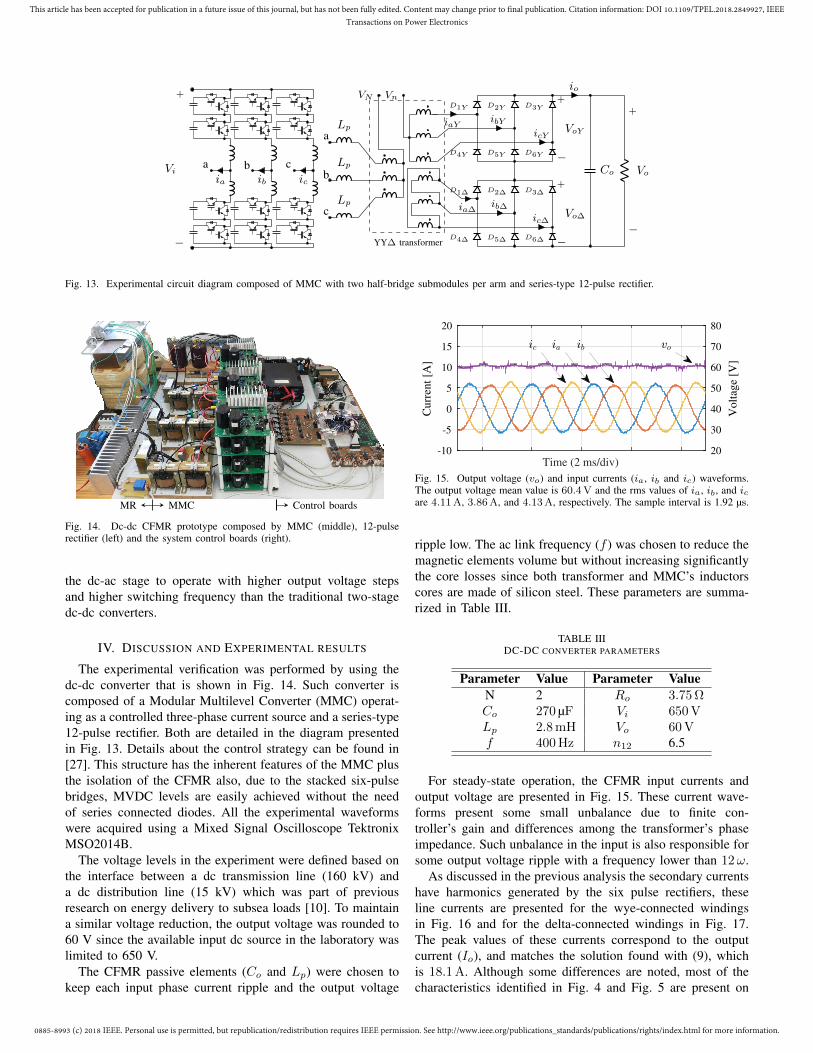
Fig. 13. Experimental circuit diagram composed of MMC with two half-bridge submodules per arm and series-type 12-pulse rectifier.
MMCMR Control boards
Fig. 14. Dc-dc CFMR prototype composed by MMC (middle), 12-pulserectifier (left) and the system control boards (right).
the dc-ac stage to operate with higher output voltage stepsand higher switching frequency than the traditional two-stagedc-dc converters.
IV. DISCUSSION AND EXPERIMENTAL RESULTS
The experimental verification was performed by using thedc-dc converter that is shown in Fig. 14. Such converter iscomposed of a Modular Multilevel Converter (MMC) operat-ing as a controlled three-phase current source and a series-type12-pulse rectifier. Both are detailed in the diagram presentedin Fig. 13. Details about the control strategy can be found in[27]. This structure has the inherent features of the MMC plusthe isolation of the CFMR also, due to the stacked six-pulsebridges, MVDC levels are easily achieved without the needof series connected diodes. All the experimental waveformswere acquired using a Mixed Signal Oscilloscope TektronixMSO2014B.
The voltage levels in the experiment were defined based onthe interface between a dc transmission line (160 kV) anda dc distribution line (15 kV) which was part of previousresearch on energy delivery to subsea loads [10]. To maintaina similar voltage reduction, the output voltage was rounded to60 V since the available input dc source in the laboratory waslimited to 650 V.
The CFMR passive elements (Co and Lp) were chosen tokeep each input phase current ripple and the output voltage
Time (2 ms/div)-10
-5
0
5
10
15
20
Cu
rren
t [A
]
20
30
40
50
60
70
80
Vo
ltag
e [V
]
Fig. 15. Output voltage (vo) and input currents (ia, ib and ic) waveforms.The output voltage mean value is 60.4 V and the rms values of ia, ib, and icare 4.11 A, 3.86 A, and 4.13 A, respectively. The sample interval is 1.92 µs.
ripple low. The ac link frequency (f ) was chosen to reduce themagnetic elements volume but without increasing significantlythe core losses since both transformer and MMC’s inductorscores are made of silicon steel. These parameters are summa-rized in Table III.
TABLE IIIDC-DC CONVERTER PARAMETERS
Parameter Value Parameter ValueN 2 Ro 3.75 ΩCo 270 µF Vi 650 VLp 2.8 mH Vo 60 Vf 400 Hz n12 6.5
For steady-state operation, the CFMR input currents andoutput voltage are presented in Fig. 15. These current wave-forms present some small unbalance due to finite con-troller’s gain and differences among the transformer’s phaseimpedance. Such unbalance in the input is also responsible forsome output voltage ripple with a frequency lower than 12ω.
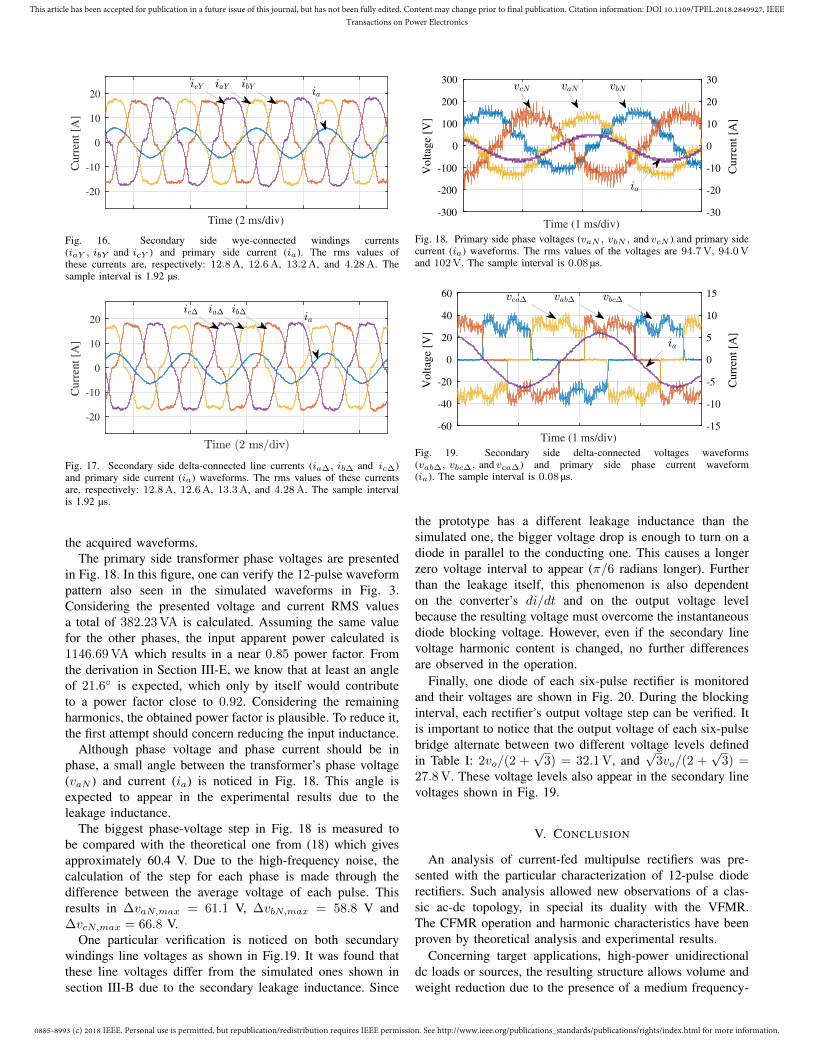
As discussed in the previous analysis the secondary currentshave harmonics generated by the six pulse rectifiers, theseline currents are presented for the wye-connected windingsin Fig. 16 and for the delta-connected windings in Fig. 17.The peak values of these currents correspond to the outputcurrent (Io), and matches the solution found with (9), whichis 18.1 A. Although some differences are noted, most of thecharacteristics identified in Fig. 4 and Fig. 5 are present on
0885-8993 (c) 2018 IEEE. Personal use is permitted, but republication/redistribution requires IEEE permission. See http://www.ieee.org/publications_standards/publications/rights/index.html for more information.
This article has been accepted for publication in a future issue of this journal, but has not been fully edited. Content may change prior to final publication. Citation information: DOI 10.1109/TPEL.2018.2849927, IEEETransactions on Power Electronics
Time (2 ms/div)
-20
-10
0
10
20
Cu
rren
t [A
]
Fig. 16. Secondary side wye-connected windings currents(iaY , ibY and icY ) and primary side current (ia). The rms values ofthese currents are, respectively: 12.8 A, 12.6 A, 13.2 A, and 4.28 A. Thesample interval is 1.92 µs.
-20
-10
0
10
20
Cu
rren
t [A
]
Fig. 17. Secondary side delta-connected line currents (ia∆, ib∆ and ic∆)and primary side current (ia) waveforms. The rms values of these currentsare, respectively: 12.8 A, 12.6 A, 13.3 A, and 4.28 A. The sample intervalis 1.92 µs.
the acquired waveforms.The primary side transformer phase voltages are presented
in Fig. 18. In this figure, one can verify the 12-pulse waveformpattern also seen in the simulated waveforms in Fig. 3.Considering the presented voltage and current RMS valuesa total of 382.23 VA is calculated. Assuming the same valuefor the other phases, the input apparent power calculated is1146.69 VA which results in a near 0.85 power factor. Fromthe derivation in Section III-E, we know that at least an angleof 21.6 is expected, which only by itself would contributeto a power factor close to 0.92. Considering the remainingharmonics, the obtained power factor is plausible. To reduce it,the first attempt should concern reducing the input inductance.
Although phase voltage and phase current should be inphase, a small angle between the transformer’s phase voltage(vaN ) and current (ia) is noticed in Fig. 18. This angle isexpected to appear in the experimental results due to theleakage inductance.
The biggest phase-voltage step in Fig. 18 is measured tobe compared with the theoretical one from (18) which givesapproximately 60.4 V. Due to the high-frequency noise, thecalculation of the step for each phase is made through thedifference between the average voltage of each pulse. Thisresults in ∆vaN,max = 61.1 V, ∆vbN,max = 58.8 V and∆vcN,max = 66.8 V.
One particular verification is noticed on both secundarywindings line voltages as shown in Fig.19. It was found thatthese line voltages differ from the simulated ones shown insection III-B due to the secondary leakage inductance. Since
Time (1 ms/div)-300
-200
-100
0
100
200
300
Vo
ltag
e [V
]
-30
-20
-10
0
10
20
30
Curr
ent
[A]
Fig. 18. Primary side phase voltages (vaN , vbN , and vcN ) and primary sidecurrent (ia) waveforms. The rms values of the voltages are 94.7 V, 94.0 Vand 102 V. The sample interval is 0.08 µs.
Time (1 ms/div)-60
-40
-20
0
20
40
60
Volt
age
[V]
-15
-10
-5
0
5
10
15
Curr
ent
[A]
Fig. 19. Secondary side delta-connected voltages waveforms(vab∆, vbc∆, and vca∆) and primary side phase current waveform(ia). The sample interval is 0.08 µs.
the prototype has a different leakage inductance than thesimulated one, the bigger voltage drop is enough to turn on adiode in parallel to the conducting one. This causes a longerzero voltage interval to appear (π/6 radians longer). Furtherthan the leakage itself, this phenomenon is also dependenton the converter’s di/dt and on the output voltage levelbecause the resulting voltage must overcome the instantaneousdiode blocking voltage. However, even if the secondary linevoltage harmonic content is changed, no further differencesare observed in the operation.
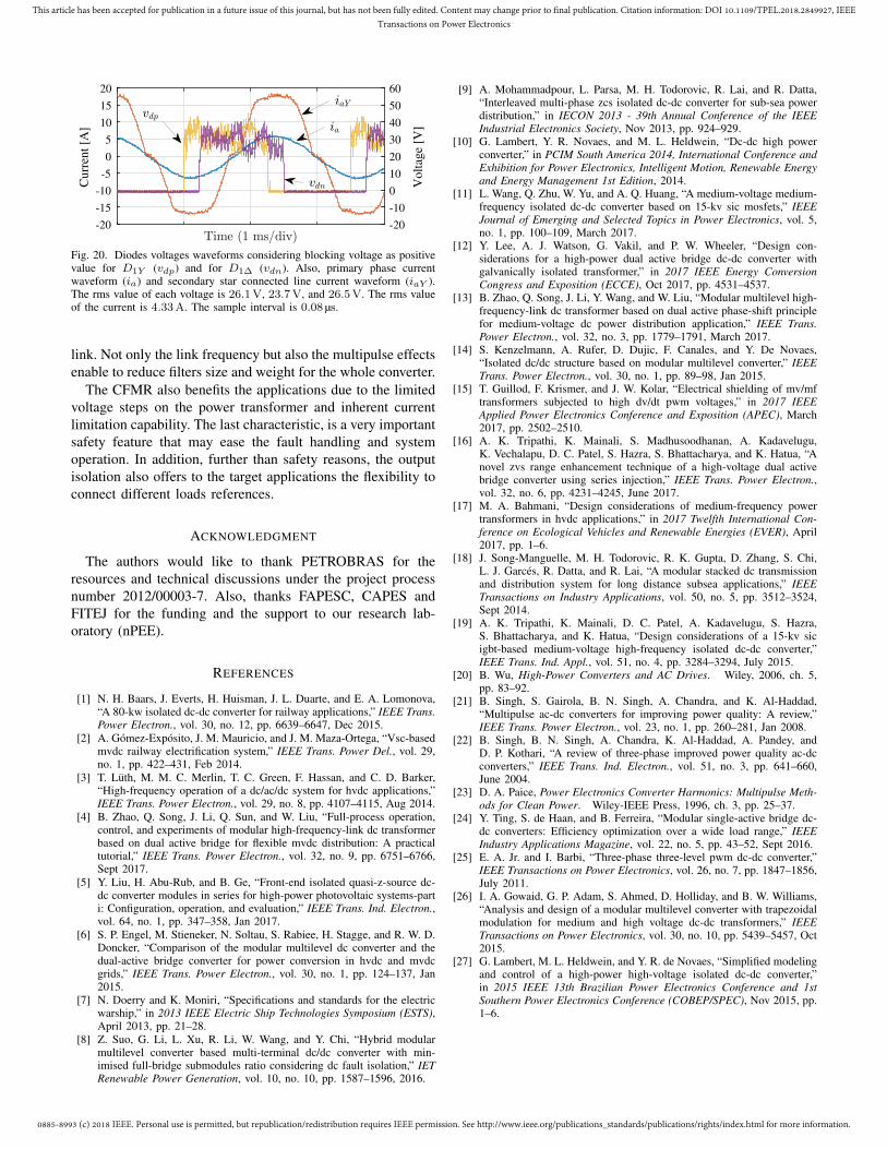
Finally, one diode of each six-pulse rectifier is monitoredand their voltages are shown in Fig. 20. During the blockinginterval, each rectifier’s output voltage step can be verified. Itis important to notice that the output voltage of each six-pulsebridge alternate between two different voltage levels definedin Table I: 2vo/(2 +
√3) = 32.1 V, and
√3vo/(2 +
√3) =
27.8 V. These voltage levels also appear in the secondary linevoltages shown in Fig. 19.
V. CONCLUSION
An analysis of current-fed multipulse rectifiers was pre-sented with the particular characterization of 12-pulse dioderectifiers. Such analysis allowed new observations of a clas-sic ac-dc topology, in special its duality with the VFMR.The CFMR operation and harmonic characteristics have beenproven by theoretical analysis and experimental results.
Concerning target applications, high-power unidirectionaldc loads or sources, the resulting structure allows volume andweight reduction due to the presence of a medium frequency-
0885-8993 (c) 2018 IEEE. Personal use is permitted, but republication/redistribution requires IEEE permission. See http://www.ieee.org/publications_standards/publications/rights/index.html for more information.
This article has been accepted for publication in a future issue of this journal, but has not been fully edited. Content may change prior to final publication. Citation information: DOI 10.1109/TPEL.2018.2849927, IEEETransactions on Power Electronics
-20
-15
-10
-5
0
5
10
15
20C
urr
ent
[A]
-20
-10
0
10
20
30
40
50
60
Vo
ltag
e [V
]
Fig. 20. Diodes voltages waveforms considering blocking voltage as positivevalue for D1Y (vdp) and for D1∆ (vdn). Also, primary phase currentwaveform (ia) and secondary star connected line current waveform (iaY ).The rms value of each voltage is 26.1 V, 23.7 V, and 26.5 V. The rms valueof the current is 4.33 A. The sample interval is 0.08 µs.
link. Not only the link frequency but also the multipulse effectsenable to reduce filters size and weight for the whole converter.
The CFMR also benefits the applications due to the limitedvoltage steps on the power transformer and inherent currentlimitation capability. The last characteristic, is a very importantsafety feature that may ease the fault handling and systemoperation. In addition, further than safety reasons, the outputisolation also offers to the target applications the flexibility toconnect different loads references.
ACKNOWLEDGMENT
The authors would like to thank PETROBRAS for theresources and technical discussions under the project processnumber 2012/00003-7. Also, thanks FAPESC, CAPES andFITEJ for the funding and the support to our research lab-oratory (nPEE).
REFERENCES
[1] N. H. Baars, J. Everts, H. Huisman, J. L. Duarte, and E. A. Lomonova,“A 80-kw isolated dc-dc converter for railway applications,” IEEE Trans.Power Electron., vol. 30, no. 12, pp. 6639–6647, Dec 2015.
[2] A. Gomez-Exposito, J. M. Mauricio, and J. M. Maza-Ortega, “Vsc-basedmvdc railway electrification system,” IEEE Trans. Power Del., vol. 29,no. 1, pp. 422–431, Feb 2014.
[3] T. Luth, M. M. C. Merlin, T. C. Green, F. Hassan, and C. D. Barker,“High-frequency operation of a dc/ac/dc system for hvdc applications,”IEEE Trans. Power Electron., vol. 29, no. 8, pp. 4107–4115, Aug 2014.
[4] B. Zhao, Q. Song, J. Li, Q. Sun, and W. Liu, “Full-process operation,control, and experiments of modular high-frequency-link dc transformerbased on dual active bridge for flexible mvdc distribution: A practicaltutorial,” IEEE Trans. Power Electron., vol. 32, no. 9, pp. 6751–6766,Sept 2017.
[5] Y. Liu, H. Abu-Rub, and B. Ge, “Front-end isolated quasi-z-source dc-dc converter modules in series for high-power photovoltaic systems-parti: Configuration, operation, and evaluation,” IEEE Trans. Ind. Electron.,vol. 64, no. 1, pp. 347–358, Jan 2017.
[6] S. P. Engel, M. Stieneker, N. Soltau, S. Rabiee, H. Stagge, and R. W. D.Doncker, “Comparison of the modular multilevel dc converter and thedual-active bridge converter for power conversion in hvdc and mvdcgrids,” IEEE Trans. Power Electron., vol. 30, no. 1, pp. 124–137, Jan2015.
[7] N. Doerry and K. Moniri, “Specifications and standards for the electricwarship,” in 2013 IEEE Electric Ship Technologies Symposium (ESTS),April 2013, pp. 21–28.
[8] Z. Suo, G. Li, L. Xu, R. Li, W. Wang, and Y. Chi, “Hybrid modularmultilevel converter based multi-terminal dc/dc converter with min-imised full-bridge submodules ratio considering dc fault isolation,” IETRenewable Power Generation, vol. 10, no. 10, pp. 1587–1596, 2016.
[9] A. Mohammadpour, L. Parsa, M. H. Todorovic, R. Lai, and R. Datta,“Interleaved multi-phase zcs isolated dc-dc converter for sub-sea powerdistribution,” in IECON 2013 - 39th Annual Conference of the IEEEIndustrial Electronics Society, Nov 2013, pp. 924–929.
[10] G. Lambert, Y. R. Novaes, and M. L. Heldwein, “Dc-dc high powerconverter,” in PCIM South America 2014, International Conference andExhibition for Power Electronics, Intelligent Motion, Renewable Energyand Energy Management 1st Edition, 2014.
[11] L. Wang, Q. Zhu, W. Yu, and A. Q. Huang, “A medium-voltage medium-frequency isolated dc-dc converter based on 15-kv sic mosfets,” IEEEJournal of Emerging and Selected Topics in Power Electronics, vol. 5,no. 1, pp. 100–109, March 2017.
[12] Y. Lee, A. J. Watson, G. Vakil, and P. W. Wheeler, “Design con-siderations for a high-power dual active bridge dc-dc converter withgalvanically isolated transformer,” in 2017 IEEE Energy ConversionCongress and Exposition (ECCE), Oct 2017, pp. 4531–4537.
[13] B. Zhao, Q. Song, J. Li, Y. Wang, and W. Liu, “Modular multilevel high-frequency-link dc transformer based on dual active phase-shift principlefor medium-voltage dc power distribution application,” IEEE Trans.Power Electron., vol. 32, no. 3, pp. 1779–1791, March 2017.
[14] S. Kenzelmann, A. Rufer, D. Dujic, F. Canales, and Y. De Novaes,“Isolated dc/dc structure based on modular multilevel converter,” IEEETrans. Power Electron., vol. 30, no. 1, pp. 89–98, Jan 2015.
[15] T. Guillod, F. Krismer, and J. W. Kolar, “Electrical shielding of mv/mftransformers subjected to high dv/dt pwm voltages,” in 2017 IEEEApplied Power Electronics Conference and Exposition (APEC), March2017, pp. 2502–2510.
[16] A. K. Tripathi, K. Mainali, S. Madhusoodhanan, A. Kadavelugu,K. Vechalapu, D. C. Patel, S. Hazra, S. Bhattacharya, and K. Hatua, “Anovel zvs range enhancement technique of a high-voltage dual activebridge converter using series injection,” IEEE Trans. Power Electron.,vol. 32, no. 6, pp. 4231–4245, June 2017.
[17] M. A. Bahmani, “Design considerations of medium-frequency powertransformers in hvdc applications,” in 2017 Twelfth International Con-ference on Ecological Vehicles and Renewable Energies (EVER), April2017, pp. 1–6.
[18] J. Song-Manguelle, M. H. Todorovic, R. K. Gupta, D. Zhang, S. Chi,L. J. Garces, R. Datta, and R. Lai, “A modular stacked dc transmissionand distribution system for long distance subsea applications,” IEEETransactions on Industry Applications, vol. 50, no. 5, pp. 3512–3524,Sept 2014.
[19] A. K. Tripathi, K. Mainali, D. C. Patel, A. Kadavelugu, S. Hazra,S. Bhattacharya, and K. Hatua, “Design considerations of a 15-kv sicigbt-based medium-voltage high-frequency isolated dc-dc converter,”IEEE Trans. Ind. Appl., vol. 51, no. 4, pp. 3284–3294, July 2015.
[20] B. Wu, High-Power Converters and AC Drives. Wiley, 2006, ch. 5,pp. 83–92.
[21] B. Singh, S. Gairola, B. N. Singh, A. Chandra, and K. Al-Haddad,“Multipulse ac-dc converters for improving power quality: A review,”IEEE Trans. Power Electron., vol. 23, no. 1, pp. 260–281, Jan 2008.
[22] B. Singh, B. N. Singh, A. Chandra, K. Al-Haddad, A. Pandey, andD. P. Kothari, “A review of three-phase improved power quality ac-dcconverters,” IEEE Trans. Ind. Electron., vol. 51, no. 3, pp. 641–660,June 2004.
[23] D. A. Paice, Power Electronics Converter Harmonics: Multipulse Meth-ods for Clean Power. Wiley-IEEE Press, 1996, ch. 3, pp. 25–37.
[24] Y. Ting, S. de Haan, and B. Ferreira, “Modular single-active bridge dc-dc converters: Efficiency optimization over a wide load range,” IEEEIndustry Applications Magazine, vol. 22, no. 5, pp. 43–52, Sept 2016.
[25] E. A. Jr. and I. Barbi, “Three-phase three-level pwm dc-dc converter,”IEEE Transactions on Power Electronics, vol. 26, no. 7, pp. 1847–1856,July 2011.
[26] I. A. Gowaid, G. P. Adam, S. Ahmed, D. Holliday, and B. W. Williams,“Analysis and design of a modular multilevel converter with trapezoidalmodulation for medium and high voltage dc-dc transformers,” IEEETransactions on Power Electronics, vol. 30, no. 10, pp. 5439–5457, Oct2015.
[27] G. Lambert, M. L. Heldwein, and Y. R. de Novaes, “Simplified modelingand control of a high-power high-voltage isolated dc-dc converter,”in 2015 IEEE 13th Brazilian Power Electronics Conference and 1stSouthern Power Electronics Conference (COBEP/SPEC), Nov 2015, pp.1–6.

0885-8993 (c) 2018 IEEE. Personal use is permitted, but republication/redistribution requires IEEE permission. See http://www.ieee.org/publications_standards/publications/rights/index.html for more information.
This article has been accepted for publication in a future issue of this journal, but has not been fully edited. Content may change prior to final publication. Citation information: DOI 10.1109/TPEL.2018.2849927, IEEETransactions on Power Electronics
Gustavo Lambert (S”14) received the B.S. andM.S. degrees in electrical engineering from theSanta Catarina State University (UDESC), Joinville,Brazil, in 2012 and 2015, respectively. He is cur-rently pursuing the Dr. degree at Santa CatarinaState University. His research interests include thedesign and control of modular multilevel convertertopologies for HVDC and MVDC applications.
Marcus V. Soares received the B. E. degree inelectrical engineering from the Santa Catarina StateUniversity, Joinville, SC, Brazil, in 2015. He iscurrently working toward the Ph.D degree at theSanta Catarina State University. His research in-terests include dc-dc converter structures for HVdctransmission and MVdc distribution networks.
Patrick Wheeler (M’00–SM’12) received his BEng[Hons] degree in 1990 from the University of Bristol,UK. He received his PhD degree in Electrical Engi-neering for his work on Matrix Converters from theUniversity of Bristol, UK in 1994. In 1993 he movedto the University of Nottingham and worked as aresearch assistant in the Department of Electricaland Electronic Engineering. In 1996 he became aLecturer in the Power Electronics, Machines andControl Group at the University of Nottingham, UK.Since January 2008 he has been a Full Professor in
the same research group. He is currently Head of the Department of Electricaland Electronic Engineering at the University of Nottingham. He is an IEEEPELs ‘Member at Large’ and an IEEE PELs Distinguished Lecturer. He haspublished 400 academic publications in leading international conferences andjournals.
Marcelo Lobo Heldwein (S”99-M”08-SM’13) re-ceived the B.S. and M.S. degrees in electricalengineering from the Federal University of SantaCatarina (UFSC), Florianopolis, Brazil, in 1997 and1999, respectively, and his Ph.D. degree from theSwiss Federal Institute of Technology (ETH Zurich),Zurich, Switzerland, in 2007.
He is currently an Associate Professor with theDepartment of Electronics and Electrical Engineer-ing at the UFSC.
From 1999 to 2003, he worked with industry,including R&D activities at the Power Electronics Institute, Brazil andEmerson Network Power, Brazil and Sweden. He was a Postdoctoral Fellowat the ETH Zurich and at the UFSC from 2007 to 2009. Dr. Heldwein is amember of the Brazilian Power Electronic Society (SOBRAEP).
His research interests include Power Electronics, Advanced Power Distri-bution Technologies and Electromagnetic Compatibility.
Yales Romulo de Novaes Yales Romulo De Novaes(IEEE member) was born in Indaial, Santa Catarina,Brazil, in 1974. In 1999 he received the B.S. degreein electrical engineering from FURB – RegionalUniversity of Blumenau, Santa Catarina, Brazil. TheM. Eng. and Dr. degrees were obtained from thePower Electronics Institute (INEP) of the FederalUniversity of Santa Catarina (UFSC) in 2000 and2006, respectively. During 2001, he worked as aresearcher engineer at the same institute. From 2006to 2008 was a post-doctoral fellow at the Industrial
Electronics Laboratory (LEI) at Ecole Polytechnique Federal de Lausanne(EPFL), Lausanne, Switzerland. From 2008 to 2010 worked as scientist withthe Power Electronics Systems group at ABB Corporate Research Center,Daetwill, Switzerland. Currently he is an associate professor at Santa CatarinaState University (UDESC), Joinville, Brazil, and coordinator of CMEAR(Research Cell on Microgrids of Alternative and Renewable Energies).