current rating for semiconductors
TRANSCRIPT

8/6/2019 Current Rating for Semiconductors
http://slidepdf.com/reader/full/current-rating-for-semiconductors 1/8
www.irf.com AN-949 1
Application Note AN-949
Current Rating of Power Semiconductors
Table of Contents
Page
What Is Current Rating?.......................................................................2
Current Ratings for Power Semiconductors.........................................2
Continuous Current Rating...................................................................3
Switching “Duty Cycle” Ratings............................................................3
Junction Temperature under Pulsed Conditions ..................................4
Peak Current Ratings...........................................................................6
Appendix ..............................................................................................6
Effect of Waveform Shape on RMS Value ...........................................7
The current rating of an electrical device, whether a circuit breaker or a motor or a transformer, isthe current at which the temperature within the electrical device reaches a value that may impairthe reliability or functionality of the device itself. The manufacturer knows the temperature limitsof the materials used in the device, but he does not know the temperature of the ambient in whichthe device will be used. So he makes an assumption on this temperature.

8/6/2019 Current Rating for Semiconductors
http://slidepdf.com/reader/full/current-rating-for-semiconductors 2/8
www.irf.com AN-949 2
AN-949
Current Rating of Power Semiconductors
1. What Is Current Rating?The current rating of an electrical device, whether a circuit breaker or a motor or a transformer, is the current at which the
temperature within the electrical device reaches a value that may impair the reliability or functionality of the device itself.
The manufacturer knows the temperature limits of the materials used in the device, but he does not know the temperature
of the ambient in which the device will be used. So he makes an assumption on this temperature. This has two important
consequences:
1) A current rating is meaningless without the rated temperature.2) The temperature at which the rating applies may, or may not be related to actual operating
conditions.
If it is, the current rating can be used as an indication of the current capability of that device in a real
application. If the device is rated at a temperature that is not encountered in a typical operating
environment, e.g. 25ºC, it cannot be trusted to provide an indication of actual device capability in an
application. It can only be used to compare the ratings of similar devices rated at the same temperature.
The rating of electrical devices like motors and circuit breakers are dictated by various agreements and regulations. The
ratings of many other devices, like transformers, resistors and semiconductors are specified in their data sheets. As a result,
the user must, minimally verify that the device is capable of operating:
a. at the maximum current
b. at the maximum ambient temperaturec. without exceeding its maximum temperature
2. Current Ratings for Power SemiconductorsLike any other electrical device, power semiconductors must be operated within their maximum temperature. Since the
vast majority of power semiconductors operate at large power densities, they require a heatsink. It is the task of the
designer to identify the heatsink, or other cooling method that fulfills the requirements of a, b and c noted in the previous
section. This task is normally referred to as “thermal design.”
Power semiconductors have, however, some additional limitations normally associated with their capability of handling
high voltages and high currents at the same time under static or dynamic conditions. These limitations are peculiar to the
specific type of semiconductor, e.g. SOA for transistors, dv/dt, di/dt and tq for thyristors, trr for diodes. Information on
these limitations is normally contained in publications that are specific to the particular device.
Bipolar transistors have one additional limitation that is not common to other power semiconductors: gain. To operate a
bipolar transistor at its headlined “rated” continuous current would require an inconveniently large amount of drive
current, and the saturation voltage and switching times would be hard to live with in a practical design.
Other power semiconductors are not limited by gain. IGBTs for motor drive applications are, by design, limited in gain to
current levels much beyond normal operating conditions to reduce the current under short-circuit conditions.

8/6/2019 Current Rating for Semiconductors
http://slidepdf.com/reader/full/current-rating-for-semiconductors 3/8
www.irf.com AN-949 3
3 . CONT INUOUS CURR ENT RA T INGS
The continuous rating of a power semiconductor is based on heat removal when conducting a fixed amount of current.
This is determined by the fundamental equation for temperature rise (see AN-936), with no switching losses present.
Rated ID, for a MOSFET is therefore:
)()(
max
JC thon DS
C J D
R R
T T I
−=
where RDS(on) is the limiting value of the on-resistance at rated T J max , at the appropriate value of I D. RthJC is the maximum
value of internal junction-to-case thermal resistance, and Tc is the case temperature.
Similarly, the continuous current rating of a diode, or a thyristor, or an IGBT is calculated from the basic equation of
temperature rise. The power dissipation is calculated from voltage drop and continuous current.
Except for water-cooled sinks, it is very difficult to keep the case temperature of a power semiconductor at less than 90ºC.
Thus, the usable continuous direct current of a power device for most practical is whatever is applicable to a case
temperature of 90 to 110° C. This allows a sufficient differential between case and ambient temperature for the heat
dissipater to handle the heat transfer.
The “headlined” continuous current rating shown on the datasheets of most power transistors is usually larger than the
practically usable level of continuous drain current. This is because the case temperature adopted by the industry, to
which the “headlined” continuous ID rating applies, is 25°C.
Figure 1 shows typical heatsinks for TO-3 and TO-220 packaged HEXFET®
Power MOSFETs that allow them to operate
in a 40°C ambient at a continuous direct drain current that is 60 to 70% of the rated continuous drain current at Tc = 25°C;
the corresponding steady case temperature is about 100°C.
The continuous current rating of power transistors is, however, of little direct use to the designer, other than as a
benchmark, for the following three reasons:
1) Power transistors are normally operated in switch mode, with duty cycles considerably less than l00%, and
what is really of interest is the current-carrying capability of the device under the actual “switched”
operating conditions.2) When operated in switch mode, power transistors have switching losses, which have to be calculated and
added to the conduction losses, as indicated in AN-936.
3) The selection of the power device may be dictated by surge requirements that make the continuous current
rating irrelevant.
If this were not enough, advances in the low-voltage MOSFET technology have reduced conduction losses to the point
that the package has become the limiting factor in their continuous current rating. This is explained in DT93-4
4 . S W ITCHING “DUT Y CYCLE” RA T INGS
The basic thermal equation of AN-936 determines the basic rating of a “thermal system” in a practical application. This
equation can be used to determine how much power can be dissipated by a (known) thermal system or the junction
temperature for a given set of electrical operating conditions (power dissipation). Since the power entered in that equationis the “average” power, it remains valid as long as the frequency of operation is high with respect to the thermal inertia of
the system. When the frequency is very low (tens of Hz), the transient thermal response curve is used, as described below
in Section 5.
The power dissipation is normally divided in conduction and switching. Conduction losses in a power MOSFET, being
resistive in nature, can be calculated as (IRMS)2
x R. The RMS content of waveforms of different shape can be found in the
Appendix. Switching losses can be calculated from the switching waveforms, from the gate charge or from analytical
methods. Conduction and switching losses for IGBTs are more complex, as explained in AN-990.

8/6/2019 Current Rating for Semiconductors
http://slidepdf.com/reader/full/current-rating-for-semiconductors 4/8
www.irf.com AN-949 4
5 . J UNCTION TEMPER AT URE UNDER PULS ED CONDITIONS
Under surge conditions the junction temperature rises
exponentially, according to its thermal inertia. Rather than using
the thermal resistance, that is appropriate for steady state
operation, we use the Transient Thermal Impedance (or, more
correctly, Thermal Response Curve), as the one shown in Figure
2. For a surge of given duration (x axis), this curve gives a
thermal response factor (y axis). The peak junction temperaturedue to the surge condition can be calculated as indicated in the
figure itself. The power dissipation is normally calculated from
the voltage and current across the device during the surge.
This curve is also useful for determining the peak junction
temperature for power or pulses with a very low repetition rate,
when the method described in the previous section is not
applicable. The reason for this is illustrated by the waveforms in
Figures 3(a) and 3(b). Both sets of waveforms are for the same
power dissipation and duty cycle, but for different operating
frequencies. The cycle-by-cycle fluctuations of junction
temperature at 20Hz (Figure 3a) are clearly greater than at
200Hz (Figure 3b). As frequency increases, thermal inertia of the junction “irons out” instantaneous temperature fluctuations
and the junction responds more to average, rather than peak
power dissipation. At frequencies above a few kHz and duty
cycles above 20% or so, cycle-by-cycle temperature fluctuations
become small, and peak junction temperature rise becomes equal
to the average power dissipation multiplied by the DC
junction-to-case thermal resistance, within one or two percent.
For pulses with low repetition rate the remaining curves in
Figure 2 show effective thermal impedance at different duty
cycles. These curves are approximately related to the single
pulse curve, by the following relationship:
Effective normalized thermal impedance = D + (l - D) x
(transient thermal impedance for single pulse of duration t).
The thermal impedance, when multiplied by the power
dissipation during the conduction period t (i.e., the power within
the conduction pulse itself, not the power averaged over the
whole cycle), gives the value of the repetitive peak
junction-to-case temperature rise.
To determine the absolute value of the peak junction temperature,
it is, of course, necessary to know the case temperature TC under
steady-state operating conditions. Because of thermal inertia, the
heatsink responds only to average power dissipation (except at
extremely low frequencies which generally will not be of
practical interest). TC is therefore given by:
TC = TA + (RthC-S + RthS-A) PAV where:
TA = ambient temperature
RthC-S = case-to-sink thermal resistance
RthS-A = sink-to-ambient thermal resistance
PAV = average power dissipation
also,
PAV = peak power x duty cycle for rectangular pulses of power
Figure 1. Typical Heatsinks for HEXFETs (Heatsink by
Wakefield)

8/6/2019 Current Rating for Semiconductors
http://slidepdf.com/reader/full/current-rating-for-semiconductors 5/8
www.irf.com AN-949 5
The transient thermal response curve assumes constant case temperature . This is generally valid for pulses shorter than
10ms. For longer surges the case temperature starts to rise and the results are of questionable accuracy. For operation in free
air, case temperature starts to rise within few milliseconds and this curve does not provide any useful information. More
sophisticated analytical methods that take the entire thermal system into account are normally used to calculate temperature
rise under these conditions.
Figure 2. Transient Thermal Impedance Curves for IRF530 HEXFET
Figure 3. Waveforms of Power and Junction Temperature for Repetitive Operation, showing
that Peak Junction Temperature is function of Operating Frequency. IRF330
8/6/2019 Current Rating for Semiconductors
http://slidepdf.com/reader/full/current-rating-for-semiconductors 6/8
www.irf.com AN-949 6
6 . PEAK CURR ENT R AT INGS
IGBTs and MOSFETs are able to carry
peak current well in excess of their
continuous current rating, provided that
the rated junction temperature is not
exceeded. There is, however, an upper
limit on the permissible current, defined
by the rated peak current. Most devices
have a peak rating, that is several times
their continuous rating at Tc = 25°C.
Power transistors are fundamentally
“linear” devices, as opposed to
“latching” devices. As current increases,
the point eventually is reached at which
they go into “linear” operation and start
to act, in effect, as a current limiter.
This point depends upon the drive
voltage applied to the gate, the safe
limit of which is determined by the
thickness of the oxide that insulates the
gate from the body of the device. Peak
ratings of power devices are normallyachievable with an applied gate voltage
that is equal to the maximum permissible gate voltage of 20V. They are repetitive ratings, as long as the junction
temperature is kept within the rated TJmax. Peak junction temperature can be calculated from the thermal impedance data
for the device, as indicated above.
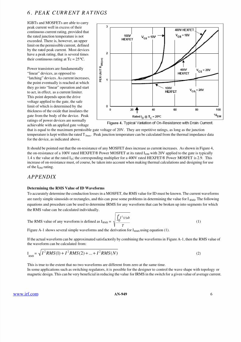
It should be pointed out that the on-resistance of any MOSFET does increase as current increases. As shown in Figure 4,
the on-resistance of a 100V rated HEXFET Power MOSFET at its rated IDM with 20V applied to the gate is typically
1.4 x the value at the rated ID; the corresponding multiplier for a 400V rated HEXFET Power MOSFET is 2.9. This
increase of on-resistance must, of course, be taken into account when making thermal calculations and designing for use
of the IDM rating.
APPENDIX
Determining the RMS Value of ID Waveforms
To accurately determine the conduction losses in a MOSFET, the RMS value for ID must be known. The current waveforms
are rarely simple sinusoids or rectangles, and this can pose some problems in determining the value for IRMS. The following
equations and procedure can be used to determine IRMS for any waveform that can be broken up into segments for which
the RMS value can be calculated individually.
The RMS value of any waveform is defined as IRMS =T
dt t I t
)(0
2
∫ (1)
Figure A-1 shows several simple waveforms and the derivation for IRMS using equation (1).
If the actual waveform can be approximated satisfactorily by combining the waveforms in Figure A-1, then the RMS value of the waveform can be calculated from:
IRMS
= )(...)2()1( 222 N RMS I RMS I RMS I +++ (2)
This is true to the extent that no two waveforms are different from zero at the same time.
In some applications such as switching regulators, it is possible for the designer to control the wave shape with topology or
magnetic design. This can be very beneficial in reducing the value for IRMS in the switch for a given value of average current.

8/6/2019 Current Rating for Semiconductors
http://slidepdf.com/reader/full/current-rating-for-semiconductors 7/8
www.irf.com AN-949 7
EFFECT OF W AVEFORM S HAPE ON RMS VALUE
In a switch mode converter, the current waveforms through the inductors, transformer windings rectifiers and switches will
appear as shown in Figure A-1, ranging from a triangle to a rectangle depending on the value of the averaging inductor and
load.
The RMS content of the current waveform changes accordingly and this has a bearing on the MOSFET conduction losses
that are proportional to I
2
RMS.
A measure of the squareness of the waveform can be obtained from the ratio: K =
b
a
I
I
It can be shown that: K = =
b
a
I
I f (L/Lc) where:
L = inductance of the averaging choke.
Lc = 1 is the critical inductance for a
Particular input voltage and load power.
As L is increased, K goes from 0 (triangle) to 1
(rectangle).
From the above expression and Iavg
=2
ba I I +
We have: Ia =1
2
+K
K Iavg
Ib =1
2
+K Iavg
Substituting into the RMS expression for atrapezoidal waveform, shown in Figure A-1, we
have:
IRMS =2
2
)1(3
12
+
++
K
K K I D avg
For constant I(avg) and D, the normalized (IRMS = 1
for K = 1) IRMS is as shown in Figure A-3. This
curve shows that, for triangular current waveforms,
the I2R losses are 32% higher than for rectangular
waveforms. It is also apparent that for Ia / Ib > 0.6,
the improvement incurred by increasing L is only2%, so from a practical point-of-view, L needs to
only be about twice LC.
Increasing the value of Ia / Ib increases the switch
turn-on losses but decreases the turn-off losses.
Since the turn-off losses tend to be larger than the
turn-on losses, increasing Ia / Ib reduces the total switching loss also. For the case of discontinuous inductor current (L < LC),
Ia / Ib = 0 and is no longer relevant, since the waveforms are now triangles. For a given Iavg the RMS current is:
32
D I I avg RMS =

8/6/2019 Current Rating for Semiconductors
http://slidepdf.com/reader/full/current-rating-for-semiconductors 8/8
www.irf.com AN-949 8