curriculum vitae december 16, 2009 - purdue engineering · mark webster received the 2002 ......
TRANSCRIPT
1
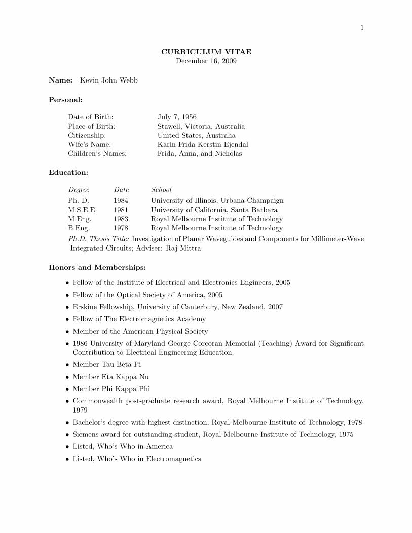
CURRICULUM VITAEDecember 16, 2009
Name: Kevin John Webb
Personal:
Date of Birth: July 7, 1956Place of Birth: Stawell, Victoria, AustraliaCitizenship: United States, AustraliaWife’s Name: Karin Frida Kerstin EjendalChildren’s Names: Frida, Anna, and Nicholas
Education:
Degree Date School
Ph. D. 1984 University of Illinois, Urbana-ChampaignM.S.E.E. 1981 University of California, Santa BarbaraM.Eng. 1983 Royal Melbourne Institute of TechnologyB.Eng. 1978 Royal Melbourne Institute of Technology
Ph.D. Thesis Title: Investigation of Planar Waveguides and Components for Millimeter-WaveIntegrated Circuits; Adviser: Raj Mittra
Honors and Memberships:
• Fellow of the Institute of Electrical and Electronics Engineers, 2005
• Fellow of the Optical Society of America, 2005
• Erskine Fellowship, University of Canterbury, New Zealand, 2007
• Fellow of The Electromagnetics Academy
• Member of the American Physical Society
• 1986 University of Maryland George Corcoran Memorial (Teaching) Award for SignificantContribution to Electrical Engineering Education.
• Member Tau Beta Pi
• Member Eta Kappa Nu
• Member Phi Kappa Phi
• Commonwealth post-graduate research award, Royal Melbourne Institute of Technology,1979
• Bachelor’s degree with highest distinction, Royal Melbourne Institute of Technology, 1978
• Siemens award for outstanding student, Royal Melbourne Institute of Technology, 1975
• Listed, Who’s Who in America
• Listed, Who’s Who in Electromagnetics

2
Professional Experience:
[July 1999 - ] Professor, School of Electrical and Computer Engineering,Purdue University, West Lafayette, IN
[June 2006 - Aug. 2007] Visiting ProfessorRoyal Institute of Technology (KTH), Stockholm
[Jan. 2003 - Dec. 2003] Visiting Professor, Dept. of Chemistry,Massachusetts Institute of Technology, Cambridge, MA
[Jan. 1990 - Jun. 1999] Associate Professor, School of Electrical and Computer Engineering,Purdue University, West Lafayette, IN
[Aug. 1984 - Dec. 1989] Assistant Professor, Electrical Engineering Department,University of Maryland, College Park, MD
Ph. D. Thesis Supervision Completed:
[1] W. A. Huting, June 1989, “Characterization of Continuous Waveguide Transitions Using aCombined Finite Element Method and Coupled Differential Equation Technique.”
[2] L. Carin, August 1989, “Characterization of Monolithic Millimeter-wave Components andVLSI Interconnects.”
[3] G. W. Slade, July 1993, “Finite Element Modeling of Electromagnetic Transmission Lines inTwo and Three Dimensions.”
[4] B. Lichtenberg, December 1994, “Finite Element Modeling of Wavelength-scale DiffractiveElements.”
[5] Y. Liu, May 1995, “Boundary Conditions and Formulations for Finite Element Electromag-netic Modeling.”
[6] T. Haq, August 1995, “Design and Fabrication of Compact Waveguide Mode Control De-vices.”
[7] K. C. Huang, August 1995, “Characterization of Resonant Tunneling Diodes.”
[8] J. S. Reynolds, February 1996, “Optical Sensing in Diffuse Media.”
[9] C. A. Thompson, August 1996, “Optical Diffusive Imaging Using Raman Spectroscopy andLaser Speckle.”
[10] E. B. Cohen, January 1998, “The Velocity Modulation Transistor - Operation, Developmentand Application.”
[11] J. C. Ye, February 1999, “Estimation and Reconstruction for the Optical Diffusion NonlinearInverse Problem.”
[12] H. J. Ueng, December 1999, “Characterization of Nonalloyed Ohmic Contacts.”
[13] M. A. Webster, December 2002, “Random Media Characterization From Laser Speckle Fre-quency Correlations.” Mark Webster received the 2002 Motorola outstanding graduate stu-dent award from the School of Electrical and Computer Engineering.

3
[14] J.-W. Lee, May 2003 (Dec. 2002 defense), “Characterization of AlGaN/GaN High ElectronMobility Transistors and Their Application in Microwave Push-Pull Amplifiers.”
[15] S. Lee, June 2004, “Intrinsic Noise Characteristics of Gallium Nitride High Electron MobilityTransistors.” Sungjae Lee received the 2004 Motorola outstanding graduate student awardfrom the School of Electrical and Computer Engineering.
[16] A. B. Milstein, August 2004, “ Imaging of Near-Infrared Fluorescence, Absorption, and Scat-ter in Turbid Media.”
[17] S. Oh, May 2005, “Nonlinear Multigrid Inversion Algorithms with Applications to StatisticalImage Reconstruction.” Seungseok Oh received a Silver 2003 Humantech Thesis Prize, at theevent hosted by Samsung Electronics, Korea, for a paper entitled ”A general framework fornonlinear multigrid inversion.”
[18] M. Yang, August 2005, “Field Transformation in Irregular Waveguide Structures and Analysisof Left-Handed Material.”
[19] J. Li , December 2005, “Nanophotonic Signal Processing Structures.”
[20] Z. Wang, December 2008.”Characterization of Random Media and Related Information Re-trieval.”
M.S. Thesis Supervision Completed:
[1] C. J. Clark, August 1986, “Investigation of new optoelectronic CW microwave source.”
[2] L. Carin, December 1986, “Computational analysis of cascaded coaxial and circular waveguidediscontinuities.”
[3] Q. Xu, May 1987, “Modal analysis of microstrip discontinuities.”
[4] P. W. Grounds, November 1987, “Numerical analysis of the finite Frequency Selective sur-face.”
[5] G. W. Slade, June 1989, “Finite Element Analysis of Integrated Waveguides.”
[6] A. Caroglanian, August 1989, “Numerical and Experimental Study of Curved and PlanarFrequency Selective Surfaces with Arbitrary Illumination.”
[7] S. S. Patrick, April 1990, “Finite Difference Analysis of Dielectric Waveguides: A VariationalApproach in Terms of the Magnetic Field Vector.”
[8] M. S. Carroll, May 1992, “Resonant Tunneling Diode Fabrication and DC Characterization.”
[9] G. E. Starnes, August 1992, “Resonant Tunneling Diode Impedance Characterization forOscillator Applications.”
[10] R. P. Lyle, May 1994, “AlGaAs/GaAs Compound Semiconductor Multiple Quantum WellOptical Reflection Modulators.”
[11] S. Lee, August 2000, “Microwave Distributed Power Amplifiers Using Gallium Nitride andSilicon Carbide Transistors.”
[12] T. Gerke, August, 2004, “Frequency-resolved interferometer measurements of polarized wavepropagation in scattering media.”

4
Research Book Contributions and Books Published:
Book Chapters:
[1] S. Lee and K. J. Webb, Low Noise Amplifiers,” Wiley Encyclopedia of RF and MicrowaveEngineering, 2004.
Research Book Contributions:
[1] Picosecond Electronics and Optoelectronics II, F. J. Leonburger, C. Lee, F. Capasso, and H.Morkoc (Ed), Springer-Verlag, 1987, C. J. Clark, E. A. Chauchard, K. J. Webb, K. Zaki, C.H. Lee, P. Polak-Dingels, H. A. Hung, and H. C. Huang, “A new optoelectronic microwavesource,” pp. 269-271.
[2] H. A. Hung, T. T. Lee, P. Polak-Dingels, E. Chauchard, K. J. Webb, C. H. Lee and H. C.Huang, “Characterization of GaAs monolithic circuits by optical techniques,” Proc. SPIE,Vol. 1102, pp. 98-106, 1987.
[3] Picosecond Electronics and Optoelectronics, Vol. 4, T.C.L.G. Sollner and D. Bloom (Ed),Optical Society of America, March 8-10, 1989; E. Chauchard, G. Treacy, K. J. Webb, C.H. Lee, H. A. Hung, H. C. Huang, and P. Polak-Dingels, “Comparison of electro-optic andphoto-conductive sampling using a 28 GHz monolithic amplifier,” pp. 52-56.
[4] T. Haq, K. J. Webb, and N. C. Gallagher, “Aperiodic grating structure for TE11 to TM11
mode conversion,” SPIE Proc., Vol. 2622, pp. 207-214, 1995.
[5] B. Lichtenberg, K. J. Webb, and N. C. Gallagher, “Finite element simulation of wavelengthscale optical elements,” SPIE Proc., Vol. 2622, 196-206, 1995.
[6] J. S. Reynolds, M. G. Erickson, and K. J. Webb, “Inexpensive instrumentation for frequencydomain detection and localization of heterogeneities utilizing diffusing optical waves,” SPIEProc., Vol. 2633, pp. 230-237, 1995.
[7] C. A. Thompson, J. S. Reynolds, F. LaPlant, D. Ben-Amotz, and K. J. Webb, “Detectionof heterogeneities within a scattering medium using Raman spectroscopy,” SPIE Proc., Vol.2622, pp. 400-404, 1995.
[8] J. S. Reynolds, F. P. LaPlant, C. A. Thompson, K. J. Webb, and D. Ben-Amotz, “Quanti-tative Raman spectroscopic study of acetonitrile in a scattering medium,” Trends in Opticsand Photonics on Biomedical Optical Spectroscopy and Diagnostics, Optical Society ofAmerica, May 1996, pp. 147-150.
[9] T. Haq, K. J. Webb, and N. C. Gallagher, “Computer generated microwave holograms asphase shifters,” SPIE Proc., Vol 3010-51, Diffractive and Holographic Device Technologiesand Applications IV, 1997.
[10] J. C. Ye, K. J. Webb, R. Millane and T. J. Downar, “Weighted cost function reconstructionin optical diffusion imaging,” SPIE Proc., Vol. 3171, Signal and Image Processing andMathematical Imaging, pp. 118-127, 1997.
[11] R. P. Millane, J. C. Ye, C. A. Bouman, and K. J. Webb, “Efficient algorithms for Bayesianoptical diffusion imaging,” Proc. Image and Vision Computing New Zealand 1999, D.Pairman and H. North (eds.), Landcare Research, Lincoln, NZ, pp. 223-228, 1999.

5
[12] K. J. Webb, J. C. Ye, C. A. Bouman, and R. P. Millane, “Nonlinear multigrid optimiza-tion for soft tissue imaging using a Bayesian optical diffusion approach,” Proc. OSA/NIHWorkshop on In Vivo Optical Imaging, Optical Society of America, 2000.
[13] A. B. Milstein, S. Oh, K. J. Webb, C. A. Bouman, and R. P. Millane, “Three-dimensional op-tical diffusion tomography using iterative coordinate descent optimization,” Photon Migra-tion, Optical Coherence Tomography, and Microscopy, S. Andersson-Engels and M. KaschkeEds., Proc. SPIE vol 4431, 2001.
[14] M. A. Webster, K. J. Webb, and A. M. Weiner, “Optical diffusion imaging data fromspeckle pattern frequency correlations,” Diagnostic Optical Spectroscopy in Biomedicine,T. Papazoglou and G. Wagnieres Eds., SPIE Vol. 4432, 2001.
[15] S. Oh, A. B. Milstein, K. J. Webb, C. A. Bouman, and R. P. Millane, “Three-dimensionalBayesian optical diffusion tomography: source-detector calibration,” Biomedical Optics:Optical Biopsy, Proc. SPIE Vol. 4613, 2002.
[16] J.-W. Lee and K. J. Webb, “Broadband push-pull microwave power amplifier using Al-GaN/GaN HEMTs on SiC,” Silicon Carbide and Related Materials 2001, pp. 1515-1518,Trans Tech Publications, Zurich, Switzerland, 2002.
[17] L. Yuan, J. A. Cooper, K. J. Webb, and M. R. Melloch, “Demonstration of IMPATTdiode oscillators in 4H-SiC,” Silicon Carbide and Related Materials 2001, pp. Trans TechPublications, Zurich, Switzerland, 2002.
[18] R. P. Millane, A. M. Milstein, Q. Zhang, S. Oh, K. J. Webb, C. A. Bouman, and D.A. Boas, “Imaging fluorescence parameters by Bayesian optical diffusion tomography,” in”Image reconstruction from incomplete data II,” P. J. Bones, M. A. Fiddy and R. P. Millane(Eds), Proc. SPIE Vol. 4792, 2002.
[19] S. Oh, A. B. Milstein, C. A. Bouman, and K. J. Webb, “Multigrid algorithms for optimiza-tions and inverse problems,” Proceedings of SPIE/IS&T Conference on ComputationalImaging, 2003.
[20] A. B. Milstein, S. Oh, K. J. Webb, and C. A. Bouman, “Estimation of kinetic modelparameters in optical diffusion tomography,” Proceedings of SPIE/IS&T Conference onComputational Imaging, 2004.
[21] S. Oh, A. B. Milstein, C. A. Bouman, and K. J. Webb, “Multigrid inversion with vari-able resolutions of data and parameter spaces,” Proceedings of SPIE/IS&T Conference onComputational Imaging, 2004.
[22] K. J. Webb, “Information in multiply scattered light,” P. J. Bones, M. A. Fiddy and R. P.Millane (Eds), Proc. SPIE Vol. 5562, 2004.
[23] S. Oh, C. A. Bouman, and K. J. Webb, ”Multigrid inversion algorithms for Poisson noisemodel-based tomographic reconstruction,” Computational Imaging, Proc. of SPIE, 2005.
Magazine Articles:
[1] A. Milstein, S. Oh, C. Bouman, K. Webb, J. Stott, D. Boas, and R. Millane, “Hiddenpictures: nonlinear Bayesian inversion methods reveal detail in fluorescence optical diffusiontomography images,” Optical Engineering Magazine, Vol. 4, No. 2, pp. 26-28, Feb. 2004.
6
[2] H. Liu and K. J. Webb, “Nanoimaging; bilayer metamaterial lens breaks the diffractionlimit,” Laser Focus World, vol. 45, no. 9, pp. 35-38, 2009.
Serial Journal Regular Articles:
[1] K. J. Webb and R. Mittra, “Dielectric waveguide grating filter,” Arch. Elek. Ubertragung.,,Vol. 38, pp. 51-54, Jan./Feb. 1984.
[2] E. G. Farr, K. J. Webb, and R. Mittra, “Studies in fin-line antenna design for imaging arrayapplications,” Arch. Elek. Ubertragung., Vol. 39, No. 2, pp. 87-89, 1985.
[3] K. J. Webb and R. Mittra, “Solution of the fin-line step discontinuity problem using thegeneralized variational technique,” IEEE Trans. Microwave Theory Tech., Vol. 33, pp.1004-1010, Oct. 1985.
[4] C. Clark, E. Chauhard, K. Webb, K. Zaki, C. Lee, H. Hung and H. Huang, “Studies of anew optoelectronic microwave source,” IEEE/OSA J. Lightwave Technol., Vol. 5, No. 3,pp. 388-397, March 1987.
[5] D. Butler, E. A. Chauchard, K. J. Webb, K. A. Zaki, C. H. Lee, P. Polak-Dingels, H.A. Hung, and H. C. Huang, “A CW 20 GHz optoelectronic source with phased arrayapplications,” Microwave and Optical Tech. Lett., Vol. 1, pp. 119-123, Jun. 1988.
[6] L. Carin, K. J. Webb, and S. Weinreb, “Matched windows in circular waveguide,” IEEETrans. Microwave Theory Tech., Vol. 36, pp. 1359-1362, Sept. 1988.
[7] K. J. Webb, A. Caroglanian, P. W. Grounds, and R. Mittra, “Numerical convergence indichroic problems,” Microwave and Optical Tech. Lett., Vol. 1, pp. 317-320, Nov. 1988.
[8] Q. Xu, K. J. Webb, and R. Mittra, “Study of modal solution procedures for microstripstep-discontinuities,” IEEE Trans. Microwave Theory Tech., Vol. 37, pp. 381-387, Feb.1989.
[9] H. A. Hung, P. Polak-Dingels, K. J. Webb, T. Smith, H. C. Huang, and C. H. Lee,“Millimeter-wave monolithic integrated circuit characterization by a picosecond optoelec-tronic technique,” IEEE Trans. Microwave Theory Tech., Vol. 37, pp. 1223-1231 Aug.1989.
[10] L. Carin and K. J. Webb, “Characteristic impedance of multilevel, multiconductor hybridmode microstrip,” IEEE Trans. Magnetics, Vol. 25, pp. 2947-2949, Jul. 1989.
[11] G. W. Slade and K. J. Webb, “A vectorial finite element analysis for integrated waveguide,”IEEE Trans. Magnetics, Vol. 25, pp. 3052-3054, Jul. 1989.
[12] W. A. Huting and K. J. Webb, “Numerical analysis of rectangular and circular waveguidetapers,” IEEE Trans. Magnetics, Vol. 25, pp. 3095-3097, Jul. 1989.
[13] L. Carin and K. J. Webb, “An equivalent circuit model for terminated hybrid-mode multi-conductor transmission lines,” IEEE Trans. Microwave Theory Tech., Vol. 37, pp. 1784-1793, Nov. 1989.
[14] W. A. Huting and K. J. Webb, “Numerical solution of the continuous waveguide transitionproblem,” IEEE Trans. Microwave Theory Tech., Vol. 37, pp. 1802-1808, Nov. 1989.

7
[15] A. Caroglanian, P. W. Grounds, and K. J. Webb, “Finite and infinite frequency selectivesurfaces: experiments and models,” J. Electromagnetic Waves and Applic., Vol. 3, No. 5,pp. 409-419, 1989.
[16] G. W. Slade, L. Carin, Q. Xu, S. E. Borchardt, and K. J. Webb, “A study of slotlineleaky-wave antennas,” IEEE Trans. Antennas Propagat, Vol. 38, pp. 411-414, 1990.
[17] L. Carin and K. J. Webb, “Isolation effects in single and dual plane VLSI interconnects,”IEEE Trans. Microwave Theory Tech., Vol. 38, pp. 396-404, Apr. 1990.
[18] K. J. Webb, P. W. Grounds, and R. Mittra, “Convergence in the spectral domain formu-lation of waveguide and scattering problems,” IEEE Trans. Antennas Propagat., Vol. 38,pp. 869-877, June 1990.
[19] L. Carin and K. J. Webb, “Pulse propagation on multi-layered circuit level interconnects,”J. Electromagnetic Waves and Applications, Vol. 4, No. 3, pp. 229-245, 1990.
[20] A Caroglanian and K. J. Webb, “Study of curved and planar frequency selective surfaceswith non-planar illumination,” IEEE Trans. Antennas Propagat., Vol. 39, pp. 211-217,Feb. 1991.
[21] W. A. Huting and K. J. Webb, “Comparison of mode matching and differential equationtechniques in the analysis of waveguide transitions,” IEEE Trans. Microwave Theory Tech.,Vol. 39, pp. 280-286, Feb. 1991.
[22] P. W. Grounds and K. J. Webb, “Numerical analysis of finite frequency selective surfaceswith rectangular patches of various aspect ratios,” IEEE Trans. Antennas Propagat., Vol.39, pp. 569-575, May 1991.
[23] G. W. Slade and K. J. Webb, “Convergence in microwave circuit parameters obtained froma vector finite element analysis,” IEEE Trans. Magnetics, Vol. 27, pp. 4048-4051, Sept.1991.
[24] S. S. Patrick and K. J. Webb, “Behavior of a magnetic field vector-based finite differenceanalysis for optical waveguides,” IEEE Trans. Magnetics, Vol. 27, pp. 3883-3885, Sept.1991.
[25] G. W. Slade and K. J. Webb, “Computation of characteristic impedance for multiple mi-crostrip transmission lines using a vector finite element method,” IEEE Trans. MicrowaveTheory Tech., Vol. 40, pp. 34-40, Jan. 1992.
[26] S. S. Patrick and K. J. Webb, “A variational vector finite difference solution for dielectricwaveguides,” IEEE Trans. Microwave Theory Tech., Vol. 40, pp. 692-698, Apr. 1992.
[27] D. L. Goeckel, K. J. Webb, and N. C. Gallagher, “Massively parallel iterative determinationof stratified dielectric parameters from scattered-field measurements,” J. Opt. Soc. Am.A, Vol. 10, No. 5, pp. 1093-1100, May 1993.
[28] K. Huang, M. S. Carroll, G. Starnes, R. Lake, D. B. Janes, K. J. Webb, and M. Melloch,“Numerically-generated resonant tunneling diode equivalent circuit parameters,” J. AppliedPhysics, Vol. 16, pp. 3850-3857, Sept. 15, 1994.
8
[29] D. B. Meade, G. W. Slade, A. F. Peterson, and K. J. Webb, “Comparison of local radiationboundary conditions for the scalar Helmholtz equation with general boundary shapes,”IEEE Trans. on Antennas Propagat., Vol. 43, pp. 6-10, Jan. 1995.
[30] T. Haq, K. J. Webb, and N. C. Gallagher, “Scattering optimization method for the design ofcompact mode converters for waveguides,” IEEE Trans. Microwave Theory and Techniques,Vol. 43, pp. 559-565, Mar. 1995.
[31] C. A. Thompson, J. S. Reynolds, F. P. LaPlant, D. Ben-Amotz, and K. J. Webb, “Ramanspectroscopic studies of diamond in Intralipid,” Optics Lett., Vol. 20, pp. 1195-1198, May1995.
[32] Y. Liu and K. J. Webb, “Variational propagation constant expressions for lossy inhomo-geneous anisotropic waveguides,” IEEE Trans. Microwave Theory Tech., Vol. 43, pp.1765-1772, Aug. 1995.
[33] D. B. Janes, K. J. Webb, M. S. Carroll, G. E. Starnes, K-C. Huang, J. Shenoy, and M. R.Melloch, “DC and microwave characterization of integrated resonant tunneling diodes,” J.Appl. Phys., Vol. 78, pp. 6616-6625, Dec. 1995.
[34] E. B. Cohen, D. B. Janes, K. J. Webb, J. N. Shenoy, J. M. Woodall, and M. R. Melloch, “A 2DEG/low-temperature-grown GaAs dual channel heterostructure transistor,” Superlatticesand Microstructures, Vol. 17, No. 4, pp. 345-349, 1995.
[35] V. R. Kolagunta, D. B. Janes, G. L. Chen, K. J. Webb, and M. R. Melloch, “Vertical three-terminal structures in semiconductor heterostructure quantum wells using a novel sidewallgating technique,” Superlattices and Microstructures, Vol. 17, No. 4, pp. 339-343, 1995.
[36] K-C. Huang, D. B. Janes, K. J. Webb, and M. R. Melloch, “An improved two-layered TLMcontact resistance characterization method,” IEEE Trans. Electron Dev., Vol. 43, No. 5,pp. 676-684, May 1996.
[37] J. S. Reynolds, A. Przadka, S. Yeung, and K. J. Webb, “Optical diffusion imaging: acomparative numerical and experimental study,” Appl. Optics, Vol. 35, No. 19, pp. 3671-3679, July 1996.
[38] B. Lichtenberg, K. J. Webb, D. B. Meade, and A. F. Peterson (Invited Paper), “Comparisonof two-dimensional conformal radiation boundary conditions,” Electromagnetics, Vol. 16,No. 4, pp. 359-384, July-Aug., 1996.
[39] T. Haq, K. J. Webb, and N. C. Gallagher, (Invited Paper), “Synthesis of waveguide modecontrol devices based on aperiodic grating,” J. Opt. Soc. of Am. A, Vol. 13, pp. 1501-1505,July 1996.
[40] V. R. Kolagunta, G. L. Chen, D. B. Janes, K. J. Webb, and M. R. Melloch, “Self-alignedsidewall gated resonant tunneling transistors,” Appl. Phys. Lett., Vol. 69, No. 3, pp.374-376, July 1996.
[41] J. S. Reynolds, C. A. Thompson, K. J. Webb, F. P. LaPlant, and D. Ben-Amotz, “Frequencydomain modeling of reradiation in highly scattering media,” Applied Optics, Vol. 36, pp.2252-2259, April 1997.
9
[42] T. Haq, K. J. Webb, and N. C. Gallagher, “Compact circular waveguide mode converters,”Microwave and Optical Tech. Lett., Vol. 13, pp. 251-255, Dec. 1996.
[43] C. A. Thompson, K. J. Webb, and A. M. Weiner, “Diffusive media characterization usinglaser speckle,” Applied Optics, Vol. 36, pp. 3726-3734, June 1, 1997.
[44] Y. Liu and K. J. Webb, “A hybrid numerical boundary condition and its approximations forelectromagnetic scattering problems,” J. Electromag. Waves & Applic., Vol. 11, 1433-1451,1997.
[45] E. B. Cohen, K. J. Webb, D. B. Janes, and M. R. Melloch, “Real space transfer in a velocitymodulated transistor,” Appl. Phys. Lett., Vol. 70, pp. 2864-2866, May 1997.
[46] M. G. Erickson, J. S. Reynolds, and K. J. Webb, “Comparison of single and dual interferingsource configurations in optical diffusion imaging,” J. Opt. Soc. Am A., Vol. 14, No. 11,pp. 3083-3092, Nov. 1997.
[47] A. Przadka, K. J. Webb, D. B. Janes, and H. C. Liu, “Microwave measurement of shot noisein resonant tunneling diodes,” Appl. Phys. Lett., Vol. 71, No. 4, pp. 530-532, July 1997.
[48] C.A. Thompson, K. J. Webb, and A.M. Weiner, “Imaging of inhomogeneities embeddedwithin scattering media using laser speckle,” J. Opt. Soc. Am. A, Vol. 14, No. 9, pp.2269-2277, September 1997.
[49] H. J. Ueng, V. R. Kolagunta, D. B. Janes, K. J. Webb, D. T. McInturff, and M. R. Mel-loch, “Annealing stability and device application of nonalloyed ohmic contacts using a lowtemperature grown GaAs cap on thin n+ GaAs layers,” Appl. Phys. Lett., Vol. 71, No. 17,pp. 2496-2498, Oct. 1997.
[50] L. Carin, G. W. Slade, and K. J. Webb, “Mode Coupling and Leakage effects in finite sizeprinted interconnects,” IEEE Trans. Microwave Theory Tech., Vol. 46, No. 5, pp. 450-457,May 1998.
[51] A. Przadka, K. J. Webb, and D. B. Janes, “Two-port noise and impedance measurementsfor two-terminal devices with a resonant tunneling diode example,” IEEE Trans. MicrowaveTheory Tech., Vol. 46, No. 9, pp. 1215-1220, Sept. 1998.
[52] M. Maheswaran, K. J. Webb, and H. J. Siegel, “A modified conjugate gradient squaredalgorithm for the solution of electromagnetic scattering problems on MIMD machines,”The Journal of Supercomputing, 14, pp. 257-280, 1999.
[53] J. C. Ye, R. P. Millane, K. J. Webb, and T. J. Downar, “Importance of the ▽D term infrequency-resolved optical diffusion imaging,” Opt. Lett., Vol. 23, pp. 1423-1425, Sept.1998.
[54] T. Haq, K. J. Webb, and N. C. Gallagher, “Optimized irregular structures for spatial andtemporal field transformation,” IEEE Trans. Microwave Theory Tech., Vol. 46, pp. 1856-1867, Nov. 1998. Invited paper.
[55] J. C. Ye, K. J. Webb, T. J Downar, and R. P. Millane, “Frechet derivative and imagereconstruction in optical diffusion tomography,” J. Opt. Soc. Am. A, vol. 16, no. 7, pp.1814-1826, July 1999.
10
[56] J. C. Ye, K. J. Webb, C. A. Bouman, and R. P. Millane, “Optical diffusion tomographyusing iterative coordinate descent optimization in a Bayesian framework,” J. Opt. Soc. Am.A, vol. 16, no. 10, pp. 2400-2412, Oct. 1999.
[57] J. D. McKinney, M. A. Webster, K. J. Webb, and A. M. Weiner, “Characterization andimaging in optically scattering media using laser speckle and a variable coherence source,”Optics Lett., vol. 25, no. 1, pp. 4-6, Jan. 2000.
[58] J. C. Ye, C. A. Bouman, K. J. Webb, and R. P. Millane, “Nonlinear multigrid algorithmsfor Bayesian optical diffusion tomography,” IEEE Trans. Image Processing, vol. 10, no. 6,pp. 909-922, June 2001.
[59] B. M. Green, S. Lee, K. Chu, K. J. Webb, and L. F. Eastman, “High efficiency monolithicGallium Nitride distributed amplifier,” IEEE Microwave Guided Wave Lett., vol. 10, No.7, pp. 270-272, July 2000.
[60] Y. Liu and K. J. Webb, “On detection of the interior resonance errors of surface inte-gral equation boundary conditions for electromagnetic scattering problems,” IEEE Trans.Antennas Propagat., vol. 49, pp. 939-943, June 2001.
[61] H. J. Ueng, D. B. Janes and K. J. Webb, “Error analysis leading to design criteria fortransmission line model characterization of ohmic contacts,” IEEE Trans. Electron Dev.,vol. 48, no. 4, pp. 758-766, April 2001.
[62] L. Yuan, J. A. Cooper, M. R. Melloch, and K. J. Webb, “Experimental demonstration of asilicon carbide IMPATT oscillator,” IEEE Electron Dev. Lett., vol. 22, no. 6, pp. 266-268,June 2001.
[63] K. J. Webb, E. B. Cohen, and M. R. Melloch, “Fabrication and operation of a velocitymodulation transistor,” IEEE Trans. Electron Dev., Vol. 48, No. 12, pp. 2701-2709, Dec.2001.
[64] H. J. Ueng, N.-P. Chen, D. B. Janes, K. J. Webb, D. T. McInturff and M. R. Melloch,“Temperature-dependent behavior of low-temperature-grown GaAs nonalloyed ohmic con-tacts,” J. Applied Phys., Vol. 90, No. 11, pp. 5637-5641, Dec. 2001.
[65] J.-W. Lee and K. J. Webb, “Broadband GaN HEMT push-pull microwave power amplifier,”IEEE Microwave Wireless Comp. Lett., Vol. 11, No. 9, pp. 367-369, Sept. 2001.
[66] B. M. Green, V. Tilak, H. Lim, J. A. Smart, K. J. Webb, J. R. Shealy, and L. F. East-man, “High-power broadband AlGaN/GaN HEMT MMIC’s on SiC substrates, IEEE Trans.Microwave Theory Tech., Vol. 49, No. 12, pp. 2486-2493, Dec. 2001.
[67] M. A. Webster, K. J. Webb, and A. M. Weiner, “Temporal response of a random mediumfrom laser speckle frequency correlations,” Phys. Rev. Lett., Vol. 88, No. 3, pp. 033901(-1-4), Jan. 2002.
[68] A. B. Milstein, S. Oh, J. S. Reynolds, K. J. Webb, C. A. Bouman, and R. P. Millane,“Three-dimensional Bayesian optical diffusion imaging using experimental data,” OpticsLett., Vol. 27, No. 2, pp. 95-97, Jan. 2002.
11
[69] S. Oh, A. B. Milstein, R. P. Millane, C. A. Bouman, and K. J. Webb, “Source-detectorcalibration in three-dimensional Bayesian optical diffusion tomography,” J. Opt. Soc. Am.A, Vol. 19, No. 10, pp. 1983-1993, Oct. 2002.
[70] S. Lee, K. J. Webb, V. Tilak, and L. F. Eastman, “Intrinsic noise equivalent circuit param-eters for AlGaN/GaN HEMTs,” IEEE Trans. Microwave Theory Tech., Vol. 51, No. 5, pp.1567-1577, May 2003.
[71] A. B. Milstein, S. Oh, K. J. Webb, C. A. Bouman, Q. Zhang, D. A. Boas, and R. P. Millane,“Fluorescence optical diffusion tomography,” Applied Optics, Vol. 42, pp. 3081-3094, June2003.
[72] M. A. Webster, K. J. Webb, A. M. Weiner, J. Y. Xu, and H. Cao, “Temporal response of arandom medium from speckle intensity frequency correlations,” J. Opt. Soc. Am. A, Vol.20, No. 11, pp. 2057-2070, Nov. 2003.
[73] J. Lee, L. F. Eastman, and K. J. Webb, “Gallium nitride push-pull microwave power am-plifiers,” IEEE Trans. Microwave Theory Tech., Vol. 51, No. 11, pp. 2243-2249, Nov.2003.
[74] M. Yang, J. Li, and K. J. Webb, “Irregular functional electromagnetic field transformationwaveguide elements,” Appl. Phys. Lett., Vol. 83, No. 14, pp. 2736-2738, Oct. 2003.
[75] J. Lee and K. J. Webb, “A temperature-dependent nonlinear analytic model for AlGaN-GaN HEMTs on SiC,” IEEE Trans. Microwave Theory Tech., Vol. 52, No. 1, pp. 2-9, Jan.2004.
[76] M. Yang, J. Li, and K. J. Webb, “Functional waveguide mode transformers,” IEEE Trans.Microwave Theory Tech., Vol. 52, No. 1, pp. 161-169, Jan. 2004.
[77] A. B. Milstein, J. J. Stott, S. Oh, D. A. Boas, R. P. Millane, C. A. Bouman, and K. J.Webb, “Fluorescence optical diffusion tomography using multiple frequency data,” J. Opt.Soc. Am. A, Vol. 21, No. 6, pp. 1035-1049, June 2004.
[78] M. A. Webster, T. D. Gerke, A. M. Weiner, and K. J. Webb, “Spectral and temporal specklefield measurements from a random medium,” Opt. Lett., Vol. 29, No. 13, pp. 1491-1493,July 2004.
[79] S. Oh, A. B. Milstein, C. A. Bouman, and K. J. Webb, “A general framework for nonlinearmultigrid inversion,” IEEE Trans. Image Processing, Vol. 14, No. 1, pp. 125-140, Jan.2005.
[80] K. J. Webb, M. Yang, D. W. Ward, and K. A. Nelson, “Metrics for negative refractive indexmaterials,” Phys. Rev. E, Vol. 70, pp. 035602(R), 2004.
[81] S. Lee and K. J. Webb, “The influence of transistor nonlinearities on noise properties,”IEEE Trans. Microwave Theory Tech., Vol. 53, No. 4, pp. 1314-1321, April, 2005.
[82] A. B. Milstein, M. D. Kennedy, P. S. Low, C. A. Bouman, and K. J. Webb, “Detection andlocalization of a fluorescent mouse tumor in a turbid medium,” Applied Optics, Vol. 44,No. 12, pp. 2300-2310, Apr. 2005.

12
[83] A. B. Milstein, K. J. Webb, and C. A. Bouman, “Estimation of kinetic model parametersin fluorescence optical diffusion tomography,” J. Opt. Soc. Am. A, Vol. 22, No. 7, pp.1357-1368, July, 2005.
[84] T. D. Gerke, M. A. Webster, A. M. Weiner, and K. J. Webb, “Frequency-resolved interfer-ometer measurements of polarized wave propagation in random media,” J. Opt. Soc. Am.A, Vol. 22, No. 12, pp. 2691-2699, Dec. 2005.
[85] M. Yang and K. J. Webb, “Poynting Vector Analysis of a Superlens,” Opt. Lett., Vol. 30,No. 18, pp. 2382-2384, Sept. 2005.
[86] S. Oh, C. A. Bouman, and K. J. Webb, “Multigrid tomographic inversion with variableresolution data and image spaces,” IEEE Trans. Im. Proc., Vol. 15, Issue 9, pp. 2805-2819, Sept. 2006.
[87] D. W. Ward, K. A. Nelson, and K. J. Webb, “On the physical origins of the negative indexof refraction,” New J. Phys., Vol. 7, pp. 213-, Oct. 2005.
[88] M. Yang, H. Chen, K. J. Webb, S. Minin, S. L. Chuang, and G. R. Cueva, “Demonstrationof Mode Conversion in an Irregular Waveguide,” Opt. Lett., Vol. 31, No. 3, pp. 383-385,Feb. 2006.
[89] K. J. Webb and J. Li, “Analysis of transmission through small apertures in conductingfilms,” Phys. Rev. B, Vol. 73, pp. 33401, 2006.
[90] K. J. Webb and J. Li, “Resonant slot optical guiding in metallic nanoparticle chains,” Phys.Rev. B Vol. 72, 201402R, 2005; also in the Virtual J. of Nanoscale Science and Technology,Dec. 5, 2005: http://www.vjnano.org.
[91] K. J. Webb and J. Li, “Waveguide cavity surface-enhanced Raman scattering,” Phys. Rev.B, Vol. 73, pp. 073404, 2006; also in the Virtual J. of Nanoscale Science and Technology,Feb. 27, 2006: http://www.vjnano.org.
[92] J. Li, G. J. Burke, D. A. White, C. A. Thompson, and K. J. Webb, “Design of near-fieldirregular diffractive optical elements using a multi-resolution direct binary search method,”Opt. Lett., Vol. 31, Issue 9, pp. 1181-1183, May 2006.
[93] K. J. Webb and M. Yang, “Sub-wavelength imaging with a multi-layer silver film structure,”Opt. Lett., Vol. 31, Issue 14, pp. 2130-2132, July 2006.
[94] K. J. Webb and M. Yang, “Generation and control of optical vortices using left-handedmaterials,” Phys. Rev. E, Vol. 74, 016601, 2006.
[95] H. Chen and K. J. Webb, “Silicon-on-insulator irregular waveguide mode converters,” Opt.Lett., Vol. 31, Issue 14, pp. 2145-2147, July 2006.
[96] Z. Wang, M. A. Webster, A. M. Weiner, and K. J. Webb, “Polarized temporal impulseresponse for scattering media from third-order frequency correlations of speckle intensitypatterns,” J. Opt. Soc. Am. A, Vol. 23, Issue 12, pp. 3045-3053, Dec. 2006.
[97] K. J. Webb and J. Li, “Resonant waveguide field enhancement in dimers,” Opt. Lett., Vol.31, Issue 22, pp. 3348-3350, Nov. 2006.
13
[98] S. Lee and K. J. Webb, “A correlated diffusion noise model for the field-effect transistor,”IEEE Trans. Computer Aided Design of Integrated Circuits, Vol. 26, No. 10, pp. 1782-1789,Oct. 2007.
[99] Z. Wang, A. M. Weiner, and K. J. Webb, “Interferometry from a scattering medium,” Opt.Lett., Vol. 32, Issue 14, pp. 2013-2015, July, 2007.
[100] G. Cao, V. Gaind, C. A. Bouman, and K. J. Webb, “Localization of an absorbing inhomo-geneity in a scattering medium in a statistical framework,” Opt. Lett., Vol. 32 No. 20, pp.3026-3028, Oct. 2007.
[101] K. J. Webb and L. Thylen, “A perfect lens material condition with a material havingadjacent absorptive and gain resonances,” Opt. Lett., Vol. 33, No. 7, pp. 747-749, Apr.2008.
[102] J. Li and K. J. Webb, “The influence of granularity in a negative refractive index lens,”Phys. Rev. A, Vol. 78, pp. 015803 (1-4), 2008.
[103] K. J. Webb and A. Ludwig, “A semiconductor quantum dot mixture as a lossless negativedielectric constant optical material,” Phys. Rev. B, Vol. 78, pp. 153303 (1-4), 2008.
[104] Shivanand, H. Liu, and K. J. Webb, “Imaging performance of an isotropic negative dielectricconstant slab,” Opt. Lett., Vol. 33, No. 21, pp. 2562-2564, Nov. 2008.
[105] H. Liu, Shivanand, and K. J. Webb, “Imaging properties of a planar uniaxial slab,” Opt.Lett., Vol. 33, No. 21, pp. 2568-2570, Nov. 2008.
[106] H. Liu, Shivanand, and K. J. Webb, “Optical circuits from anisotropic films,” Phys. Rev.B, Vol. 79, No. 9, pp. 094203, Mar. 2009.
[107] H. Liu, Shivanand, and K. J. Webb, “Subwavelength imaging with non-magnetic anisotropicbilayers,” ‘Opt. Lett., Vol. 34, No. 14, pp. 2243-2245, July 2009.
[108] V. Gaind, K. J. Webb, S. Kularatne, and C. A. Bouman, “Towards in vivo imaging ofintramolecular fluorescence resonance energy transfer parameters,” J. Opt. Soc. Am. A,Vol. 26, No. 8, pp. 1805-1813, Aug. 2009. Highlighted in OSA Spotlight on Optics.
[109] G. Cao, C. A. Bouman, and K. J. Webb, “Non-iterative MAP reconstruction using sparsematrix representations,” IEEE Trans. Image Proc. , Vol. 18, No. 9, pp. 2085-2099, Sept.2009.
[110] J. Li and K. J. Webb, “Terahertz field enhancement in doped semiconductor slot cavities,”J. Appl. Phys. (to appear).
Pending Journal Publications (Under Review, Revision, Preparation):
[111] Z. Wang, A. M. Weiner, and K. J. Webb, “Coherent incident field information from specklecorrelations over source position with thick random scattering media.”
[112] K. J. Webb and Shivanand, “Negative electromagnetic field energy in dispersive materials.”
[113] E. R. Statz, K-H. Lin, K. A. Nelson, M. Yang, and K. J. Webb, “Direct measurement ofTHz electric fields within a frequency dependent TM mode converter,” Opt. Lett.
14
[114] V. Gaind, S. Kularatne, P. S. Low, and K. J. Webb, ”Deep tissue imaging of intramolecularfluorescence resonance energy transfer parameters,” Opt. Lett.
[115] A. Ludwig and K. J. Webb, “On the accuracy of effective medium parameter extractionprocedures for optical metamaterials,” Phys. Rev. B.
[116] H. Liu and K. J. Webb, “An anisotropic metamaterial leaky waveguide,” Phys. Rev. B.
[117] H. Liu and K. J. Webb, “Approximate Green’s function for a uniaxially anisotropic slab,”Opt. Lett.
Conference Proceedings and Presentations:
[1] K. J. Webb, E. G. Farr and R. Mittra, “Dielectric waveguide filters for millimeter waves,“ Di-gest of the fifth annual Electromagnetics, Propagation and Communication Affiliates Work-shop, p. 9, University of Illinois, April 7,8 1983.
[2] E. G. Farr, K. J. Webb and R. Mittra, “Studies in fin-line antenna design for phased arrayapplications,” Digest of the sixth annual Electromagnetics, Propagation and CommunicationAffiliates Workshop, p. 8, University of Illinois, April 5,6 1984.
[3] K. J. Webb and R. Mittra, “An overview of the spectral domain analysis of fin-line discon-tinuities using the method of moments,” pp. 64-66, Proc. IEEE Antennas and Propagationand Microwave Theory and Techniques Benjamin Franklin Symposium on Advances in An-tenna and Microwave Technology, Philadelphia, PA, May 8, 1985.
[4] K. J. Webb and R. Mittra, “Conjugate gradient iterative solution of an integral equationwith a small number of Green’s function terms: the fin-line discontinuity problem,” Digestof 1985 North American Radio Science (URSI) Meeting, p. 161, June 17-21, Vancouver,Canada.
[5] K. J. Webb and R. Mittra, “A variational solution of the fin-line discontinuity problem,”pp. 311-316, Proc. European Microwave Conf., Paris, France, September 1985.
[6] K. J. Webb and R. Mittra, “Numerical solution of planar integrated circuit discontinuitieswith unknowns in the plane of the metalization,” Digest of 1986 North American RadioScience (URSI) Meeting, p. 172, June 9-13, Philadelphia, PA.
[7] C. Clark, E. Chauchard, K. Webb, K. Zaki, C. Lee, H. Hung and H. Huang, “Generation ofCW microwaves by an optoelectronic technique,” pp. 605-608, Proc. 11th Int. Conferenceon Infrared and Millimeter Waves, October 20-24, 1986, Tirrenia-Pisa, Italy.
[8] K. J. Webb, L. Carin, and Q. Xu, “Numerical analysis of planar high frequency integratedcircuit geometries,” pp. C26-C30, Digest of the IEEE workshop on Electromagnetic FieldComputation, October 20-21, 1986, Schenectady, NY.
[9] C. J. Clark, E. A. Chauchard, K. J. Webb, K. Zaki, C. H. Lee, P. Polak-Dingels, H. A.Hung, H. C. Huang, “A new optoelectronic microwave source,” Digest of the Topical Meetingon Picosecond Electronics and Optoelectronics, pp. 176-178, January 14-16, 1987, InclineVillage, Nevada.

15
[10] C. J. Clark, E. A. Chauchard, K. J. Webb, K. Zaki, C. H. Lee, P. Polak-Dingels, H. Hung,H. Huang, “Monolithic microwave and millimeter-wave phased array applications of a newoptoelectronic source,” pp. 74-76, Proc. Antennas and Propagation and Microwave Theoryand Techniques Benjamin Franklin Symposium on Advances in Antenna and MicrowaveTechnology, Cherry Hill, NJ, March 21, 1987.
[11] L. Carin, K. J. Webb, and Q. Xu, “A theoretical study of cross-talk associated with highspeed digital integrated circuits,” pp. 81-84, Proc. Antennas and Propagation and Mi-crowave Theory and Techniques Benjamin Franklin Symposium on Advances in Antennaand Microwave Technology, Cherry Hill, NJ, March 21, 1987.
[12] L. Carin, Q. Xu, K. J. Webb, and J. McClintock, “Analysis of VLSI interconnect structures,”pp. 625-628, Proc. 1987 IEEE Microwave Theory and Techniques Society InternationalMicrowave Symposium, Las Vegas, NV, June 9-11, 1987.
[13] Q. Xu, K. J. Webb, and R. Mittra, “Modal analysis of shielded microstrip discontinuities,”Digest of North American Radio Science (URSI) Meeting, p. 29, Blacksburg, VA, June15-19, 1987.
[14] G. W. Slade, L. Carin. Q. Xu, and K. J. Webb, “Experimental results for a W-band leaky-wave finline antenna,” Digest of North American Radio Science (URSI) Meeting, p. 154,Blacksburg, VA, June 15-19, 1987.
[15] P. Grounds and K. J. Webb, “Analysis of a finite frequency selective surface,” Digest ofNorth American Radio Science (URSI) Meeting, p. 254, Blacksburg, VA, June 15-19, 1987.
[16] H.A. Hung, T. Smith, H.C. Huang, P. Polak-Dingels, K. J. Webb, and C.H. Lee, “Opticalelectronic characterization of monolithic millimeter-wave integrated circuits,” Proc. 12thInt. Conference on Infrared and Millimeter Waves, pp. 87-88, December 14-18, 1987,Orlando, FL.
[17] D. Butler, E.A. Chauchard, K. J. Webb, K.A. Zaki, C.H. Lee, P. Polak-Dingels, H.A.Hung, and H.C. Huang, “A new optoelectronic continuous wave millimeter-wave source,”Proc. 12th Int. Conference on Infrared and Millimeter Waves, pp. 140-141, December14-18, 1987, Orlando, FL.
[18] P. Polak-Dingels, H.A. Hung, T. Smith, H.C. Huang, K. J. Webb, and C.H. Lee, “On-wafer characterization of monolithic millimeter-wave integrated circuits by a picosecondoptical electronic technique,” Proc. of IEEE Microwave Theory and Techniques SocietyInternational Microwave Symposium, pp. 237-240, New York, NY, May 25-27, 1988.
[19] P. W. Grounds and K. J. Webb, “Numerical analysis of finite frequency selective surfaces,”Digest of the IEEE Antennas and Propagation Society (AP-S) Symposium, pp. 746-749,Syracuse, NY, June 1988.
[20] K. J. Webb, P. W. Grounds, and R. Mittra, “Aspects of convergence in the spectral domainformulation of EM problems,” Digest of the URSI Symposium, p. 284, Syracuse, NY, June1988.
[21] W. A. Huting, J. A. Krill, and K. J. Webb, “New developments in circular overmodedwaveguide,” Digest of the North American Radio Science (URSI) Meeting, p. 202, Syracuse,NY June 1988.
16
[22] P. Polak-Dingels, H. A. Hung, K. J. Webb, T. Smith, H. C. Huang, and C. H. Lee, “Anoptoelectronic technique for S-parameter measurements of millimeter-wave monolithic in-tegrated circuits,” Digest of the 13th Conference on Infrared and Millimeter Waves, pp.69-70, Dec. 1988, Honolulu, Hawaii.
[23] L. Carin and K. J. Webb, “Hybrid mode analysis of multi-layered microstrip,” Digest ofIEEE Computational Electromagnetics Conference, p. 75, Washington, DC, Dec. 12-14,1988.
[24] G. W. Slade and K. J. Webb, “A vectorial finite element analysis for integrated structures,”Digest of IEEE Computational Electromagnetics Conference, p. 136, Washington, DC, Dec.12-14 1988.
[25] W. A. Huting and K. J. Webb, “Numerical solution of the waveguide transition problem,”Digest of IEEE Computational Electromagnetics Conference, p. 155, Washington, DC, Dec.12-14, 1988.
[26] E. Chauchard, G. Treacy, K. Webb, C. Lee, H. Hung, H. Huang, and P. Polak-Dingels,“Comparison of electro-optic and photoconductive sampling using a 28 GHz monolithicamplifier,” Digest of the IEEE Picosecond Electronics and Optoelectronics Conference, pp.75-77, March 8-10, 1989, Salt Lake City, Utah.
[27] H. A. Hung, T. T. Lee, P. Polak-Dingels, E. Chauchard, K. J. Webb, C. H. Lee, and H.C. Huang, “Characterization of GaAs monolithic circuits by optical techniques,” Digest ofSociety of Photo-Instrumentation Engineers Meeting on Optical Technology for MicrowaveApplications 4, vol. 1102, pp. 98-106, Mar. 28-29, 1989, Orlando, FL.
[28] K. J. Webb, (Invited Speaker), “On-wafer optoelectronic characterization of MMIC’s,” pagepublished handout at IEEE Electro Conference, New York, Apr. 11-13, 1989.
[29] K. J. Webb, (Invited Speaker), E. A. Chauchard, P. Polak-Dingels, C. H. Lee, H. Hung, andH. Huang, “A time-domain network analyzer which uses optoelectronic techniques,” Digestof IEEE Microwave Theory and Techniques Society International Microwave Symposium,pp. 217-220, Long Beach, CA, Jun. 13-15, 1989.
[30] A. Caroglanian and K. J. Webb, “Curved and planar frequency selective surfaces witharbitrary illumination,” Digest of IEEE Antennas and Propagation Society Meeting, pp.1060-1063, San Jose, CA Jun. 26-30, 1989.
[31] G. W. Slade, L. Carin and K. J. Webb, “Effects of conductor thickness on the characteristicsof multiconductor microstrip,” Digest of Progress of Electromagnetics Research Symposium(PIERS), p. 247,248 Boston, MA, Jul. 25-26, 1989.
[32] L. Carin, G. W. Slade, and K. J. Webb, “Modal transition phenomena in shielded microstripwith anisotropic substrates,” Digest of 1990 IEEE Microwave Theory and Techniques So-ciety Symposium, pp. 677-680, Dallas TX, May 8-10.
[33] A. Caroglanian and K. J. Webb, “Application of the infinite FSS spectral domain methodin solving finite planar FSS problems with arbitrary illumination,” Digest of 1990 IEEEAntennas and Propagation Society Symposium, p. 112, Dallas TX, May 7-11.
17
[34] G. W. Slade, L. Carin, and K. J. Webb, “Mode transitions in dual microstrip on sapphireand Epsilam-10 substrates,” Digest of 1990 North American Radio Science (URSI) Meeting,p. 228, Dallas TX, May 7-11.
[35] G. W. Slade and K. J. Webb, “Computation of microwave circuit parameters using a vectorfinite element analysis,” IEEE Computational Electromagnetics Conference, Toronto, Oct.22-24, 1990, p. DB-9.
[36] S. S. Patrick and K. J. Webb, “A vectorial finite difference method for dielectric waveguidesbased upon a variational approach,” IEEE Computational Electromagnetics Conference,Toronto, Oct. 22-24, 1990, p. PA-10.
[37] K. J. Webb, “Interconnect modeling,” presented at the Semiconductor Research Corporation(SRC) TRC on IC Package Design, Analysis and Simulation, Stanford University, May 17,1991.
[38] G. W. Slade and K. J. Webb, “Numerical aspects of computing circuit parameters of mul-ticonductor transmission lines on substrates with tensor permittivities using a vector finiteelement method,” Proceedings of Progress in Electromagnetic Research Symposium, p. 307,Boston, MA, July 1-5, 1991.
[39] G. W. Slade and K. J. Webb, “Calculation of attenuation in waveguides with general cross-sections using the finite element method,” Digest of the North American Radio ScienceMeeting, p. 397, London, Ontario, Canada, June 24-28, 1991.
[40] G. W. Slade, L. Carin and K. J. Webb, “Dispersion and circuit properties of striplines onanisotropic substrates: numerical and experimental results,” Digest of the North AmericanRadio Science Meeting, p. 398, London, Ontario, Canada, June 24-28, 1991.
[41] K. J. Webb, “Modeling interconnects for the twenty-first century,” Semiconductor ResearchCorporation TRC on Package Design, Analysis and Simulation Systems, University of Ari-zona, Tucson, May 13, 1992 (2 pages).
[42] D. B. Meade, G. W. Slade, A. F. Peterson, and K. J. Webb, “Analytic evaluation of theaccuracy of several conformable local absorbing boundary conditions,” Digest of 1992 IEEEAntennas and Propagation Symposium Digest, pp. 540-543, July 18-25, Chicago, IL.
[43] G. W. Slade and K. J. Webb, “Waveguide radiation boundary condition for three dimen-sional finite element models,” Digest of the 1992 IEEE Conference on Electromagnetic FieldComputation, p. MOD2, Aug. 3-5, Claremont, CA.
[44] D. L. Goeckel, K. J. Webb, N. C. Gallagher, T. A. Gosink, and J. J. Kelley, “Microwaveand optical measurements and parallel computation for the determination of sea ice char-acteristics,” Proceedings of the 8th International Symposium on Okhotsk Sea and Sea Ice,Mombetsu, Hokkaido, Japan, Jan. 31 - Feb. 5, 1993, P-29, pp. 533-537.
[45] D. L. Goeckel, K. J. Webb, and N. C. Gallagher, “Inverse scattering computations for strat-ified media problems using massively parallel computers,” Digest of 1993 IEEE Antennasand Propagation Symposium, pp. 524-427, Ann Arbor, June 27 - July 2, 1993.
[46] D. B. Meade, A. F. Peterson, and K. J. Webb, “Radiation boundary conditions for thevector Helmholtz equation,” Digest of North American Radio Science (URSI) Meeting, p.255, Ann Arbor, June 27-July 2, 1993.

18
[47] G. W. Slade and K. J. Webb, “Computing port parameters and eigenmodes for structuresloaded with general lossy materials,” Digest of North American Radio Science (URSI)Meeting, p. 183, Ann Arbor, June 27-July 2, 1993.
[48] L. Carin, G. W. Slade, K. J. Webb, and A. A. Oliner, “Packaged printed transmissionlines: modal phenomena and relation to leakage,” Digest of IEEE Microwave Theory andTechniques Symposium, pp. 1195-1198, Atlanta, June 14-18, 1993.
[49] K. J. Webb Invited Speaker, 1993 IEEE Microwave Theory and Techniques Symp. Workshopon Combined Self-Consistent Particle Transport Simulation and Full Wave Dynamic FieldSimulation for Monolithic Solid State Device and Circuit Calculations, “Electromagneticinterconnect and packaging modeling,” and “Integrated resonant tunneling diodes,” Atlanta,June 18, 1993.
[50] K. J. Webb, G. W. Slade, Y. Liu, and M. Gerhold, “Field modeling of interconnects,”Digest of Semiconductor Research Corporation TECHCON, pp. 170-172, Sept. 28-30,1993, Atlanta.
[51] G. W. Slade, M. Gerhold, Y. Liu, and K. J. Webb, “Field modeling of interconnects -poster,” Semiconductor Research Corporation TECHCON, Sept. 28-30, 1993, Atlanta.
[52] R. Lyle, M. Aquilina, A. Kuver, M. Austin, K. Webb, M. Melloch, and D. Nolte, “Fabrica-tion and testing of novel hybrid Fabry-Perot surface-normal optical modulators,” AustralianCompound Optoelectronic Materials and Devices Conference, 6-8 Dec. 1993, Australian Na-tional University, Canberra.
[53] R. Lyle, R. Egan, A. Clark, A. Kuver, M. Austin, and K. Webb, “Design and fabrication ofMOCVD-grown III-V blue light modulators,” IREE 18th Australian Conference on OpticalFibre Technology, Nov. 28 - Dec. 1, 1993, Wollongong, NSW.
[54] T. Haq, K. J. Webb, and N. C. Gallagher, “Aperiodic gratings in waveguides,” OpticalSociety of America Annual Meeting, June 6-8, 1994, Rochester, NY.
[55] T. Haq, K. J. Webb, and N. C. Gallagher, “Scattering optimization synthesis of compactmode converters for waveguides,” Digest of IEEE Antennas and Propagation Symposium,pp. 1668-1671, Seattle, WA, June 19-24, 1994.
[56] B. Lichtenberg, Y. Liu, J. Reynolds, K. Webb, and D. Meade, “Applications and perfor-mance of a local conformal radiation boundary condition,” Digest of IEEE Antennas andPropagation Symposium, pp. 406-409, Seattle, WA, June 19-24, 1994.
[57] D. B. Meade, Y. Liu, B. Lichtenberg, and K. J. Webb, “A comparison of radiation boundarycondition strategies for Helmholtz equations,” Proceedings of IMACS Conference (4 pages),Atlanta, GA, July 1994.
[58] B. Lichtenberg, N. Gallagher, and K. Webb, (Invited Speaker) “Finite element simulationof wavelength scale optical devices,” Presented at the Optical Society of America AnnualMeeting, Dallas, TX, Oct. 2-7, 1994.
[59] J. Reynolds, S. Yeung, A. Przadka, J. Walters, K. Webb, and N. Gallagher, “Frequencydomain detection and localization of heterogeneities in tissue-like media,” Presented atOptical Society of America Annual Meeting, Dallas, TX, Oct. 2-7, 1994.
19
[60] J. S. Reynolds and K. J. Webb, “Optical diffusion imaging,” First Purdue Workshop onMedical Imaging, Aug. 30, 1994.
[61] T. Haq, K. J. Webb (Invited Speaker), and N. C. Gallagher, “Aperiodic grating for TE02 toTE01 conversion in a highly overmoded circular waveguide,” Digest of the Optical Societyof America Topical Meeting on Signal Recovery and Synthesis, pp. 31-33, Mar. 12-17, 1995,Salt Lake City, Utah.
[62] D. B. Janes, V. R. Kolagunta, G. Chen, and K. J. Webb, “Fabrication of vertical three-terminal structures in semiconductor heterostructure quantum wells using a novel sidewallgating technique,” Presented at the American Physical Society Meeting, March 1995, SanJose, CA.
[63] T. Haq, K. J. Webb, and N. C. Gallagher, “Aperiodic grating structure for TE11 toTM11 mode conversion,” Presented at Society of Photo-Instrumentation Engineers Meeting,Chicago, IL, May 18-19, 1995.
[64] J. S. Reynolds, M. Erickson, K. J. Webb, and N. C. Gallagher, “Inexpensive instrumentationfor frequency domain detection and localization of heterogeneities utilizing diffusing opticalwaves,” Presented at Society of Photo-Instrumentation Engineers Meeting, Chicago, IL,May 18-19, 1995.
[65] C. A. Thompson, J. S. Reynolds, F. P. LaPlant, D. Ben-Amotz, and K. J. Webb, “Ra-man measurements in Intralipid,” Presented at Society of Photo-Instrumentation EngineersMeeting, Chicago, IL, May 18-19, 1995.
[66] B. Lichtenberg, K. J. Webb, and N. C. Gallagher, “Finite element simulation of wavelengthscale optical elements,” Presented at Society of Photo-Instrumentation Engineers Meeting,Chicago, IL, May 18-19, 1995.
[67] T. Haq, K. J. Webb, and N. C. Gallagher, “TE11 to TM11 compact mode converter for cir-cular waveguide,” Digest of IEEE Microwave Theory and Techniques Society InternationalMicrowave Symposium, pp. 1613-1615, May 15-19, 1995, Orlando, FL.
[68] J. S. Reynolds, M. G. Erickson, K. J. Webb, and N. C. Gallagher, “Optical diffusion imagingwith single and multiple sources,” Digest of OSA/IEEE/APS Conf. on Lasers and Electro-Optics, p. 298, May 22-26, 1995, Baltimore, MD.
[69] C. A. Thompson, J. S. Reynolds, F. P. LaPlant, D. Ben-Amotz, and K. J. Webb, “Ramanspectroscopic detection of inhomogeneities embedded within a scattering medium,” Digestof OSA/IEEE/APS Conf. on Lasers and Electro-Optics, p. 96, May 22-26, 1995, Baltimore,MD.
[70] T. Haq, K. J. Webb, and N. C. Gallagher, “Application of the scattering optimizationmethod for the design of circular waveguide mode converters,” Digest of IEEE Antennasand Propagation Symposium and International Radio Science Meeting, pp. 718-721, June18-23, 1995, Newport Beach, CA.
[71] N. Kapadia, B. Lichtenberg, J. A. B. Fortes, J. L. Gray, H. J. Siegel, and K. J. Webb(Invited Speaker), “Parallel solution of unstructured sparse finite element equations,” Digestof IEEE Antennas and Propagation Symposium and International Radio Science Meeting,pp. 1330-1333, June 18-23, 1995, Newport Beach, CA.
20
[72] Y. Liu and K. J. Webb, “Detection of the interior resonance errors of surface integralboundary conditions for scattering problems,” Digest of IEEE Antennas and PropagationSymposium and International Radio Science Meeting, pp. 1029-1032, June 18-23, 1995,Newport Beach, CA.
[73] Y. Liu and K. J. Webb, “An exact hybrid numerical boundary condition for electromagneticscattering problems,” Digest of IEEE Antennas and Propagation Symposium and Interna-tional Radio Science Meeting, pp. 1480-1483, June 18-23, 1995, Newport Beach, CA.
[74] J. S. Reynolds, M. G. Erickson, and K. J. Webb, “Imaging in highly scattering media withRF-modulated optics,” Presented at Workshop on Applications of Radio Science, Canberra,Australia, June 25-27, 1995.
[75] T. Haq, K. J. Webb, and N. C. Gallagher, “Optimization-based waveguide mode conver-sion,” Presented at Workshop on Applications of Radio Science, Canberra, Australia, June25-27, 1995.
[76] K-C. Huang, V. Kolagunta, A. Przadka, H. Ueng, N-P. Chen, D. B. Janes, K. J. Webb,M. R. Melloch, and J. Woodall, “High-speed applications of quantum electronic devices,”Presented at Workshop on Applications of Radio Science, Canberra, Australia, June 25-27,1995.
[77] V. Kolagunta, G. Chen, D. B. Janes, K. J. Webb, and M. R. Melloch, “Vertical three-terminal structures in semiconductor heterostructure quantum wells using a novel sidewallgating technique,” Proc. 8th Int. Conf. on Superlattices, Microstructures and Microdevices,p. I-1 (3 pages), Cincinnati, Aug. 20-25, 1995.
[78] K-C. Huang, D. B. Janes, K. J. Webb, and M. R. Melloch, “A study of physically-basedequivalent circuit model of resonant tunneling diodes,” Proc. 8th Int. Conf. on Super-lattices, Microstructures and Microdevices, p. XVII-2 (2 pages), Cincinnati, Aug. 20-25,1995.
[79] E. B. Cohen, J. N. Shenoy, D. B. Janes, K. J. Webb, J. M. Woodall, and M. R. Melloch, “A2 DEG/low-temperature-grown GaAs dual channel heterostructure transistor,” Proc. 8thInt. Conf. on Superlattices, Microstructures and Microdevices, p. I-6 (3 pages), Cincinnati,Aug. 20-25, 1995.
[80] J. S. Reynolds, M. G. Erickson, and K. J. Webb, “Optical diffusion: scanning, source con-figuration, boundary conditions, and resolution,” Presented at Optical Society of AmericaAnnual Meeting, Portland, OR, Sept. 10-15, 1995.
[81] K. J. Webb, Y. Liu, B. Lichtenberg, T. Haq, and N. C. Gallagher, “Optical applicationsof the finite element method,” Presented at Optical Society of America Annual Meeting,Portland, OR, Sept. 10-15, 1995.
[82] C. A. Thompson, K. J. Webb, and A. M. Weiner, “Speckle characterization of diffusemedia,” Presented at Optical Society of America Annual Meeting, Portland, OR, Sept.10-15, 1995.
[83] D. B. Janes, V. R. Kolagunta, G. Chen, K. J. Webb, and M. R. Melloch, “Resonant tun-neling devices with direct sidewall gates,” Digest of The Electrochemical Society 3rd. Int.Symp. on Quantum Confinement, Chicago, IL, Oct. 8-13, 1995 (2 pages).

21
[84] V. Kolugunta, D. B. Janes, G. Chen, K. J. Webb, and M. R. Melloch, “Side-gated res-onant tunneling transistors,” International Semiconductor Device Research Symposium,Charlottesville, VA, Dec. 6-8, 1995.
[85] J. S. Reynolds, F. P. LaPlant, C. A. Thompson, K. J. Webb, and D. Ben-Amotz, “Ramanmeasurements of concentrations in scattering media,” Optical Society of America TopicalMeeting on Biomedical Optical Spectroscopy and Diagnostics, March 18-22, 1996, Orlando.
[86] A. Przadka, H. Ueng, N. Chen, K. Webb, D. Janes, and M. Melloch, “Broadband microwavenoise characterization of resonant tunneling diodes,” American Physical Society Meeting,March 1996, St. Louis, MO.
[87] V. Kolagunta, G. Chen, D. Janes, K. Webb, and M. Melloch, “Sidewall gated resonanttunneling diodes for low-dimensional device studies,” American Physical Society Meeting,March 1996, St. Louis, MO.
[88] E. Cohen, D. Janes, K. Webb, M. Melloch, D. McInturff, and J. Woodall, “Dual-channeldouble-gated real space transfer device,” American Physical Society Meeting, March 1996,St. Louis, MO.
[89] V. R. Kolagunta, G. L. Chen, D. B. Janes, K. J. Webb, and M. R. Melloch, “Three terminalresonant tunneling devices with direct sidewall gates,” Third International Symposium onNanostructures and Mesoscopic Systems, Santa Fe, NM, May 19-24, 1996.
[90] A. Przadka, H. Ueng, K. J. Webb, D. B. Janes, and M. R. Melloch, “Microwave mea-surements of the intrinsic shot noise in a double barrier resonant tunneling diode,” ThirdInternational Symposium on Nanostructures and Mesoscopic Systems, Santa Fe, NM, May19-24, 1996.
[91] T. Haq and K. J. Webb, “Smooth surface discretization for the design of waveguide modeconverters,” Presented at IEEE Antennas and Propagation and Radio Science Symposium,July 21-26, 1996, Baltimore, MD.
[92] C. A. Thompson, K. J. Webb, and A. M. Weiner, “Imaging of inhomogeneities withinscattering media using laser speckle,” Optical Society of America Annual Meeting, Oct.20-24, 1996, Rochester, NY.
[93] T. Haq, K. J. Webb (Invited Speaker), and N. C. Gallagher, “Computer generated microwaveholograms as phase shifters,” SPIE Photonics West, San Jose, CA, Feb. 8-14, 1997. Oralpaper withdrawn, but paper published in SPIE Vol. 3010-51, Diffractive and HolographicDevice Technologies and Applications IV, 1997.
[94] A. Przadka, K. J. Webb, D. B. Janes, and H. C. Liu, “Suppressed noise in resonant tunnelingdiodes at microwave frequencies,” American Physical Society March Meeting, Kansas City,MO, Mar. 17-21, 1997.
[95] K. J. Webb, E. B. Cohen, D. B. Janes, M. Melloch, and C. Wilshere, “Real space transferbetween two semiconductor channels connected in parallel,” American Physical SocietyMarch Meeting, Kansas City, MO, Mar. 17-21, 1997.
[96] J. C. Ye, K. J. Webb, T. J. Downar, and R. P. Millane, “Weighted cost-function recon-struction in optical diffusion imaging,” Proc. Society of Photo-Instrumentation Engineers
22
Symp. on Signal and Image Processing and Mathematical Imaging, Vol. 3171, pp. 118-127,San Diego, CA July 27 - Aug. 1, 1997.
[97] E. B. Cohen, K. J. Webb, D. B. Janes, and M. R. Melloch, “Demonstration of a velocitymodulated transistor,” Device Research Conference, Fort Collins, CO, June 23-25, 1997.
[98] V. Kolagunta, H. J. Ueng, D. B. Janes, K. J. Webb, D. I. McInturff, M. R. Melloch, andJ. M. Woodall, “Study of low-temperature grown GaAs cap layers in device applications,”39th Materials Research Conference, Fort Collins, CO, June 25-27, 1997.
[99] A. M. Weiner and K. J. Webb (Invited Presentation), “Optical Speckle Imaging,” OpticalSociety of America Annual Meeting, Oct. 12-17, 1997, Long Beach, CA.
[100] J. C. Ye, K. J. Webb, R. Millane, and T. J. Downar, “A weighted distorted born iterativemethod for optical diffusion imaging,” Optical Soc. Am. Annual Meeting, Oct. 12-17, 1997,Long Beach, CA.
[101] M. G. Erickson, J. S. Reynolds, and K. J. Webb, “Numerical evaluation of interfering photondensity waves for imaging in highly scattering media,” Optical Society of America AnnualMeeting, Oct. 12-17, 1997, Long Beach, CA.
[102] J. C. Ye, K. J. Webb, R. P. Millane, and T. J. Downar, “Optimal parameter updatingfor optical imaging,” IEEE Int. Conf. on Image Processing, Chicago, Oct. 4-7, 1998, pp.390-393.
[103] J. C. Ye, R. P. Millane, K. J. Webb, and T. J. Downar, “The effect of the ▽D term inoptical diffusion imaging,” Optical Society of America Signal Recovery and Synthesis TopicalMeeting, Kona, Hawaii, June 1998.
[104] K. J. Webb (Invited Speaker), “Optimized mesoscopic optical diffractive elements,” OpticalSociety of America Annual Meeting, Baltimore, MD, Oct. 1998.
[105] J. C. Ye, K. J. Webb, R. P. Millane, and T. J. Downar, “Unified parameter estimation al-gorithm for diffusion imaging using the optimal search,” Optical Society of America AnnualMeeting, Baltimore, MD, Oct. 1998.
[106] J. C. Ye, C. A. Bouman, and K. J. Webb, “A localized relaxation algorithm for Bayesiandiffusion tomography using the generalized Gaussian Markov random field prior model,”Optical Society of America Annual Meeting, Baltimore, MD, Oct. 1998.
[107] E. B. Cohen, D. B. Janes, K. J. Webb, and M. R. Melloch, “A technique for determination offree carrier concentration profiles in backgated heterostructures,” 40th. Electronic MaterialsConference, Charlottesville, VA, June 24-26, 1998.
[108] H-J. Ueng, V. R. Kolagunta, D. B. Janes, K. J. Webb, D. T. McInturff, M. R. Melloch,and J. M. Woodall, “Low temperature GaAs-based nonalloyed ohmic contacts as planarinjectors for devices,” em 40th Electronic Materials Conference, Charlottesville, VA, June24-26, 1998.
[109] M. Maheswaran, K. J. Webb, and H. J. Siegel “Reducing the synchronization overhead inparallel nonsymmetric Krylov algorithms on MIMD machines,” 1998 International Confer-ence on Parallel Processing (ICPP ’98), co-sponsors: International Association for Com-puters and Communications and The Ohio State University, pp. 405-413, Minneapolis, MN,Aug. 1998.

23
[110] J. McKinney, M. Webster, K. J. Webb, and A. M. Weiner, “Characterization of thickscattering media via speckle measurements using a tunable coherence source,” IEEE Conf.on Lasers and Electro-Optics, Baltimore, MD, May 23-28, 1999.
[111] N. P. Chen, H-J. Ueng, D. B. Janes, K. J. Webb, and M. R. Melloch, “A model for contactresistance of a non-alloyed ohmic contact utilizing low-temperature-grown GaAs,” AmericanPhysical Society Meeting, March 20-29, 1999, Atlanta, GA.
[112] N. P. Chen, D. B. Janes, K. J. Webb, and M. R. Melloch, “Experimentally verified conduc-tion model for a low-resistance non-alloyed ohmic contact utilizing low-temperature-grownGaAs,” Electronic Materials Conference, June 30-July 2, 1999, University of California,Santa Barbara.
[113] J. C. Ye and K. J. Webb, “Comparative analysis of the variational PDE and Born-typeintegral equation approaches for optical diffusion tomography,” IEEE Antennas and Prop-agation Symposium and National Radio Science Meeting, July 11-16, 1999, Orlando, FL.
[114] J. C. Ye, C. A. Bouman, K. J. Webb and R. P. Millane, “Optical diffusion tomography usingiterative coordinate descent optimization in a Bayesian framework,” SPIE Conference onMathematical Modeling, Bayesian Estimation, and Inverse Problems, Denver, CO, July1999.
[115] C. A. Bouman, J. C. Ye, K. J. Webb, and R. P. Millane, “Fast Inverse Algorithms for OpticalDiffusion Tomography,” (invited paper) NSF conference on DSP for Sampled CoherentAperture Systems: Challenges, Synergies and Extensions, Charlottesville, Virginia, July7-9, 1999.
[116] J. C. Ye, C. A. Bouman, R. P. Millane, and K. J. Webb, “Nonlinear multigrid optimizationfor Bayesian diffusion tomography,” IEEE International Conference on Image Processing,October 25-28, 1999, Kobe, Japan.
[117] K. J. Webb (Invited Speaker), J. C. Ye, C. A. Bouman, and R. P. Millane, “Optimization-based optical diffusion tomography,” Optical Society of America Annual Meeting, Sept. 26- Oct. 1, 1999, Santa Clara, CA.
[118] M. A. Webster, J. D. McKinney, A. M. Weiner and K. J. Webb, “Coherence requirementsfor laser speckle imaging in diffuse media,” Optical Society of America Annual Meeting,Sept. 26 - Oct. 1, 1999, Santa Clara, CA.
[119] K. J. Webb, S. Lee, and J. Lee, “Gallium nitride broadband distributed power amplifier,”1st Gallium Nitride Electronic Device Workshop, Cornell Univ., Ithaca, NY, August 16-17,1999.
[120] K. J. Webb, J. C. Ye, C. A. Bouman, and R. P. Millane, “Nonlinear multigrid optimizationfor soft tissue imaging using a Bayesian optical diffusion approach,” NIH Workshop on InVivo Optical Imaging, Bethesda, MD, September 16-17, 1999.
[121] R. P. Millane, J. C. Ye, C. A. Bouman, and K. J. Webb, “Efficient algorithms for Bayesianoptical diffusion imaging,” Imaging and Vision Computing ’99, Aug. 30-31, 1999, TheUniversity of Canterbury, Christchurch, New Zealand.
24
[122] J. C. Ye, C. A. Bouman, R. P. Millane, and K. J. Webb (Invited Speaker), “Nonlinearmultigrid optical diffusion tomography,” OSA Biomedical Topical Meetings: Workshop onDiffuse Optical Tomography, April 2-5, 2000, Miami, FL.
[123] M. A. Webster, J. D. McKinney, A. M. Weiner, and K. J. Webb, “Using laser specklestatistics and a variable coherence source for imaging in diffuse media,” OSA BiomedicalTopical Meetings, April 2-5, 2000, Miami, FL.
[124] M. A. Webster, J. D. McKinney, A. M. Weiner, and K. J. Webb, “Obtaining photon transittime distribution of diffuse media using laser speckle statistics for imaging applications,”IEEE Conference on Lasers and Electro-Optics, May 5 - 12, 2000, San Francisco, CA.
[125] S. Lee, B. Green, K. Chu, K. J. Webb, and L. F. Eastman, “Demonstration of a highefficiency nonuniform monolithic gallium nitride distributed amplifier,” IEEE InternationalMicrowave Symposium, June 11-16, 2000, Boston, MA.
[126] R. P. Millane, C. A. Bouman, K. J. Webb, and J. C. Ye, “Multigrid Bayesian methodsfor optical diffusion tomography,” SPIE International Symposium on Optical Science andTechnology (Image Reconstruction and Incomplete Data), July 30 - August 4, 2000, SanDiego, CA.
[127] K. J. Webb, J. C. Ye, C. A. Bouman, and R. P. Millane, “Optical diffusion imaging us-ing nonlinear multigrid optimization,” European Conference on Lasers and Electro-Optics,September 10-15, 2000, Nice, France.
[128] K. J. Webb, M. A. Webster, J. D. McKinney, and A. M. Weiner, “Variable coherence indetermining the scattering parameters of diffuse media using laser speckle,“ InternationalQuantum Electronics Conference, September 10-15, 2000, Nice, France.
[129] L. Yuan, J. A. Cooper, M. R. Melloch, and K. J. Webb, ”Design, fabrication, and character-ization of the first SiC IMPATT diodes,” ONR Microwave Workshop, South Padre Island,TX, October 23 - 25, 2000.
[130] C. A. Bouman, J. C. Ye, K. J. Webb, and R. Millane (Invited Paper ), “Nonlinear multigridoptimization with applications to optical diffusion tomography,” 34th Annual Conferenceon Information Sciences and Systems, March 15-17, 2000, Princeton, NJ.
[131] S. Lee, B. M. Green, J. Lee, K. J. Webb, and L. F. Eastman, “High efficiency GaN cascode-connected HEMT nonuniform distributed amplifier,” Proc. Cornell/IEEE Conference onAdvanced Concepts in High Performance Devices, pp. 79-81, Aug. 2000.
[132] R. P. Millane, C. A. Bouman, K. J. Webb, and J. C. Ye, “Multigrid optimization andapplication to optical diffusion imaging,” Proc. Image and Vision Computing New Zealand2000, M.J. Cree and A. Steyn-Ross (Eds), Waikato University, Hamilton, NZ, 62-67, 2000.
[133] R. P. Millane, C. A. Bouman, K. J. Webb, and J. C. Ye, “Nonlinear multigrid optimizationfor image reconstruction,” New Zealand Mathematics Colloquium 2000, Hamilton, NZ, 27-29 Nov. 2000.
[134] B. M. Green, V. Tilak, S. Lee, H. Kim, J. A. Smart, K. J. Webb, J. R. Shealy, and L. F.Eastman, “High power broadband AlGaN/GaN HEMT MMICs on SiC substrates,” IEEEInternational Microwave Symposium, Phoenix, AZ, May 20-25, 2001.
25
[135] J.-W. Lee and K. J. Webb, “A low-loss planar microwave balun with an integrated biasscheme for push-pull amplifiers,” IEEE International Microwave Symposium, Phoenix, AZ,May 20-25, 2001.
[136] J.-W. Lee, S. Lee and K. J. Webb, “Scalable large-signal device model for high power-densityAlGaN/GaN HEMTs on SiC,” IEEE International Microwave Symposium, Phoenix, AZ,May 20-25, 2001.
[137] K. J. Webb, M.-C. Yang, and J.-H. Li, “Synthesis and performance of irregular fieldtransformation Elements,” IEEE Antennas and Propagation International Symposium andUSNC/URSI National Radio Science Meeting, Boston, MA, July 8-13, 2001.
[138] A. B. Milstein, S. Oh, K. J. Webb, and C. A. Bouman, “Three-dimensional optical dif-fusion imaging in a Bayesian framework,” IEEE Conference on Lasers and Electo-Optics,Baltimore, MD, May 6-11, 2001 (CLEO Technical Digest pp. 400-401).
[139] M. A. Webster, K. J. Webb, and A. M. Weiner, “Time-domain response of a diffusivemedium from speckle pattern frequency correlations,” Quantum Electronics and Laser Sci-ence (QELS) Symp., Baltimore, MD, May 6-11, 2001 (Digest pp. 142-143).
[140] K. J. Webb, A. Milstein, S. Oh, C. A. Bouman, and R. P. Millane, “Three-dimensional opti-cal diffusion imaging with detector noise,” CLEO/Europe European Conference on Biomed-ical Optics, Munich, Germany, June 18-21, 2001.
[141] K. J. Webb, M. A. Webster, and A. M. Weiner, “Optical diffusion imaging data from specklepattern frequency correlations,” CLEO/Europe European Conference on Biomedical Optics,Munich, Germany, June 18-21, 2001.
[142] L. Yuan, M. R. Melloch, J. A. Cooper, and K. J. Webb, “An X-band silicon carbide IMPATTdiode,” 59th Device Research Conference, University of Notre Dame, IN, June 25-27, 2001(Digest pp. 207-208).
[143] J.-W. Lee, S. Lee and K. J. Webb, “Demonstration of push-pull operation of AlGaN/GaNHEMTs on SiC,” 59th Device Research Conference, University of Notre Dame, IN, June25-27, 2001 (Digest pp. 203-204).
[144] K. J. Webb, M.-C. Yang, and J.-H. Li, “Synthesis of irregular field transformation struc-tures,” Optical Society of America Annual Meeting, Long Beach, CA, Oct. 14-18, 2001.
[145] S. Oh, A. Milstein, J. S. Reynolds, K. J. Webb, C. A. Bouman and R. P. Millane, “Re-constructing optical diffusion images from multiple modulation frequency measurements,”Optical Society of America Annual Meeting, Long Beach, CA, Oct. 14-18, 2001.
[146] M. A. Webster, K. J. Webb, and A. M. Weiner, “Frequency dependent correlations ofspeckle patterns from a scattering medium,” Optical Society of America Annual Meeting,Long Beach, CA, Oct. 14-18, 2001.
[147] J.-W. Lee and K. J. Webb, “Broadband push-pull microwave power amplifier using Al-GaN/GaN HEMTs on SiC,” International Conference on Silicon Carbide and Related Ma-terials, Tsukuba, Japan, Oct. 28 - Nov. 2, 2001 (Digest pp. 683-684).
26
[148] L. Yuan, J. A. Cooper, K. J. Webb, and M. R. Melloch, “Demonstration of IMPATT diodeoscillators in 4H-SiC,” International Conference on Silicon Carbide and Related Materials,Tsukuba, Japan, Oct. 28 - Nov. 2, 2001 (Digest pp. 723-724).
[149] S. Oh, A. B. Milstein, R. P. Millane, C. A. Bouman, and K. J. Webb, “Three-dimensionalBayesian optical diffusion tomography with source-detector calibration,” IEEE and OpticalSociety of America Symposium on Signal Recovery and Synthesis, Albuquerque, NM, Nov.5-8, 2001.
[150] M. A. Webster, K. J. Webb, and A. M. Weiner, “Third order speckle intensity correlationsfor obtaining the temporal response of a diffusely scattering medium,” IEEE and OpticalSociety of America Symposium on Signal Recovery and Synthesis, Albuquerque, NM, Nov.5-8, 2001.
[151] J.-W. Lee, B. M. Green, S. Lee, J. R. Shealy, L. F. Eastman, and K. J. Webb, “BroadbandGaN push-pull microwave power amplifiers,” International Semiconductor Device ResearchSymposium, Washington, DC, Dec. 5-7, 2001
[152] A. B. Milstein, S. Oh, K. J. Webb, C. A. Bouman, R. P. Millane, “Three-dimensionalBayesian optical diffusion tomography,” SPIE Conference on Optical Biopsy IV, San JoseCalifornia, January 21-23, 2002.
[153] M. Yang and K. J. Webb, “Functionality of optical field transformation in irregular waveg-uide structures,” IEEE/OSA Conf. Lasers and Electro-Optics, May 20-24, 2002, LongBeach, CA.
[154] A. B. Milstein, S. Oh, K. J. Webb, C. A. Bouman, and R. P. Millane, “Imaging of fluo-rescence, absorption, and scattering properties in diffuse media using pump and emissionwavelength measurements,” Digest of the IEEE/OSA Conf. Lasers and Electro-Optics, pp.558-559, May 20-24, 2002, Long Beach, CA.
[155] M. A. Webster, K. J. Webb, and A. M. Weiner, “Third order speckle intensity frequencycorrelations for random media characterization,” IEEE/OSA Conf. Lasers and Electro-Optics, May 20-24, 2002, Long Beach, CA.
[156] A. B. Milstein, S. Oh, K. J. Webb, C. A. Bouman, and R. P. Millane, “Three-dimensionalBayesian optical diffusion tomography with fluorescence,” OSA Biomedical Topical Meetings(Advances in Optical Imaging and Photon Migration), April 7-10, Miami Beach, FL.
[157] A. B. Milstein, Q. Zhang, S. Oh, K. J. Webb, C. A. Bouman, R. P. Millane, and D. A.Boas, “Fluorescence imaging in optical diffusion tomography,” Digest of IEEE Int. Symp.on Biomedical Imaging: Macro to Nano, pp. 58-61, July 7-10, 2002, Washington, DC.
[158] M. Yang and K. J. Webb, “High functionality mode transformers with bandwidth controland mode selectivity,” IEEE Int. Microwave Symp., June 2-7, 2002, Seattle WA.
[159] S. Lee, V. Tilak, K. J. Webb and L. F. Eastman, “Intrinsic noise characteristics of Al-GaN/GaN HEMTs,” IEEE Int. Microwave Symp., June 2-7, 2002, Seattle WA.
[160] J.-W. Lee and K. J. Webb, “Analysis and design of low-loss planar microwave baluns havingthree symmetric coupled lines,” IEEE Int. Microwave Symp., June 2-7, 2002, Seattle WA.
27
[161] M. Yang and K. J. Webb, “Synthesis of irregular waveguide field transformation elementsusing a multi-resolution algorithm,” IEEE Int. Antennas and Propagation and Radio Sci-ence (URSI) Symp., San Antonio, TX, June 16-21, 2002.
[162] J. Li and K. J. Webb, “Synthesis of multilayer aperiodic scattering structures,” IEEE Int.Antennas and Propagation and Radio Science (URSI) Symp., San Antonio, TX, June 16-21,2002.
[163] S. Lee, K. J. Webb, V. Tilak, and L. F. Eastman, “Intrinsic AlGaN/GaN HEMT noisefrom a measurement-based equivalent circuit model,” 2002 International Device ResearchConference, Santa Barbara, CA, June 24-26, 2002 (Late News Paper).
[164] K. J. Webb, A. B. Milstein, M. D. Kennedy, K. N. Jallad, C. A. Bouman, and P. S. Low,“Folate conjugate fluorescence labeling for tumor localization,” National Institutes of HealthWorkshop on Optical Imaging, Bethesda, MD, Sept. 26-27, 2002.
[165] M. Yang, H. Chen, J. Li, and K. J. Webb, “Wavelength-scale rectangular waveguide fieldtransformer realization,” OSA Annual Meeting, Orlando, FL, Sept. 29 - Oct. 3, 2002.
[166] S. Oh, A. B. Milstein, C. A. Bouman, and K. J. Webb, “Multigrid algorithms for optimiza-tion and inverse problems,” SPIE Conference on Computational Imaging, San Jose, CA,Jan. 22-24, 2003.
[167] M. Yang, J. Li, H. Chen and K. J. Webb, “Near-field functional field transformation struc-tures,” IEEE/OSA Conf. Lasers and Electro-Optics, Baltimore, MD, June 1-6, 2003.
[168] A. B. Milstein, S. Oh, C. A. Bouman, and K. J. Webb, “Imaging from time-resolved flu-orescence in turbid media,” IEEE/OSA Conf. Lasers and Electro-Optics, Baltimore, MD,June 1-6, 2003.
[169] M. Yang, J. Li, H. Tsai, and K. J. Webb, “Field transformation in irregular waveguides,”American Physical Society Meeting, March 3-7, 2003, Austin, TX.
[170] M. Yang, J. Li, H. Tsai, and K. J. Webb, “Wavelength-scale functional waveguide modeconversion,” a Conference on Lasers and Electro-Optics, Pacific Rim, Taiwan, Dec. 2003.
[171] S. Oh, A. B. Milstein, C. A. Bouman, and K. J. Webb, ”Nonlinear multigrid inversion,”2003 IEEE Conference on Image Processing, Sept. 2003, Barcelona, Spain.
[172] S. Oh, A. B. Milstein, C. A. Bouman, and K. J. Webb, “Adaptive nonlinear multigrid in-version with applications to Bayesian optical diffusion tomography,” Proc. IEEE Workshopon Statistical Signal Processing, St. Louis, MO, Sept. 2003.
[173] D. W. Ward, E. Statz, M. Yang, K. A. Nelson, and K. J. Webb (Invited Speaker), “Imagingand waveguide elements with periodic or negative refractive index materials,” Progressin Electromagnetics Research Symp. and DARPA Workshop on Left-Handed Materials,Honolulu, Oct. 13-16, 2003.
[174] T. D. Gerke, M. A.Webster, A. M. Weiner, and K. J. Webb, “Random and ensembleoptical fields from scattering media using frequency-resolved interferometer measurements,”CLEO/IQEC Conference, San Francisco, California, May 16-21, 2004.
28
[175] Z. Wang, M. A. Webster, K. J. Webb, and A. M. Weiner, “Study of scattering media withpolarized coherent light,” CLEO/IQEC Conference, San Francisco, California, May 16-21,2004.
[176] A. B. Milstein, S. Oh, C. A. Bouman, and K. J. Webb, “Mutual information as a perfor-mance measure for fluorescence optical diffusion tomography,” CLEO/IQEC Conference,San Francisco, California, May 16-21, 2004.
[177] D. W. Ward, E. Statz, K. J. Webb, and K. A. Nelson, “The role of multiferroics in thenegative index of refraction,” Fundamental Physics of Ferroelectrics, 2004 conference.
[178] Z. Wang, T. D. Gerke, M. A. Webster, A. M. Weiner, and K. J. Webb, “Polarizationproperties of speckle from scattering media,” American Physical Society Meeting, Montreal,Quebec, Canada, March 22-26, 2004.
[179] M. Yang, J. Li, H. Chen, K. J. Webb, P. Kondratko, S. L. Chuang, and G. Cueva,“Nanometer-scale optical signal processing using irregular conducting-wall waveguides,”American Physical Society Meeting, Montreal, Quebec, Canada, March 22-26, 2004.
[180] S. Lee, K. J. Webb, and L. F. Eastman, “The Influence of transistor nonlinearities onintrinsic noise,” IEEE International Microwave Symposium, Fort Worth, Texas, June 6-11,2004.
[181] S. Lee and K. J. Webb, “Numerical noise model for the AlGaN/GaN HEMT,” IEEE Inter-national Microwave Symposium, Fort Worth, Texas, June 6-11, 2004.
[182] A. B. Milstein, S. Oh, C. A. Bouman, and K. J. Webb, “Estimation of kinetic modelparameters in optical diffusion tomography,” Proc. of the SPIE/IS&T Conference on Com-putational Imaging, San Jose, CA, Jan. 2004.
[183] S. Oh, A. B. Milstein, C. A. Bouman, and K. J. Webb, “Multigrid inversion with variableresolution data and parameter spaces,” Proc. of the SPIE/IS&T Conference on Computa-tional Imaging, San Jose, CA, Jan. 2004.
[184] A. Milstein, S. Oh, K. J. Webb, C. A. Bouman, “Direct reconstruction of kinetic parameterimages in fluorescence optical diffusion tomography,” IEEE ISBI, Washington, DC, April15-18, 2004.
[185] K. J. Webb (Invited Speaker), “Information in multiply scattered light,”Image Reconstruc-tion from Incomplete Data, SPIE, Aug. 2-6, 2004, Denver CO.
[186] M. Yang, J. Li, H. Chen, K. J. Webb, and G. Cueva, “Field transformation and phase controlin µm-scale metallic waveguides,” OSA Frontiers in Optics, Oct. 10-14, 2004, Rochester,NY.
[187] Z. Wang, M. A. Webster, A. M. Weiner, and K. J. Webb, “Polarization-dependent charac-terization of scattering media using intensity correlations,” OSA Frontiers in Optics, Oct.10-14, 2004, Rochester, NY.
[188] A. B. Milstein, S. Oh, C. A. Bouman, and K. J. Webb, “Kinetic fluorescence optical diffusiontomography,” OSA Frontiers in Optics, Oct. 10-14, 2004, Rochester, NY.
29
[189] S. Oh, C. A. Bouman, and K. J. Webb, ”Multigrid inversion algorithms for Poisson noisemodel-based tomographic reconstruction”, SPIE Conf. on Computational Imaging III, SanJose, California, Jan. 2005.
[190] K. J. Webb and J. Li, “The physical basis of enhanced transmission through small aperturesin metallic films,” American Physical Society Meeting, March 21-25, 2005, Los Angeles, CA.
[191] K. J. Webb and J. Li, “Nanoparticle material and geometry requirements for surface-enhanced Raman scattering,” American Physical Society Meeting, March 21-25, 2005, LosAngeles, CA.
[192] K. J. Webb, M. Yang, D. W. Ward, and K. A. Nelson, “Imaging potential of a negativerefractive index lens,” American Physical Society Meeting, March 21-25, 2005, Los Angeles,CA.
[193] D. W. Ward, K. A. Nelson, and K. J. Webb, “Negative refraction in the polariton regime:an illustration of a nonlinear process in negative refractive materials,” American PhysicalSociety Meeting, March 21-25, 2005, Los Angeles, CA.
[194] D. W. Ward, E. R. Statz, K. A. Nelson, and K. J. Webb, “Polaritonic bandgap materials fab-ricated and tested with femtosecond laser machining and polariton imaging,” CLEO/IQECConference, May 23-26, 2005, Baltimore, MD.
[195] K. J. Webb, M. Yang, D. W. Ward, and K. A. Nelson, “Resolution limits of a negativerefractive index lens,” CLEO/IQEC Conference, May 23-26, 2005, Baltimore, MD.
[196] S. Oh, A. B. Milstein, C. A. Bouman, and K. J. Webb, “Nonlinear multigrid inversion foroptical diffusion tomography,” CLEO/IQEC Conference, May 23-26, 2005, Baltimore, MD.
[197] A. B. Milstein, C. A. Bouman, K. J. Webb, M. D. Kennedy, and P. S. Low, “A statis-tical approach for detection and localization of a fluorescing mouse tumor in Intralipid,”CLEO/IQEC Conference, May 23-26, 2005, Baltimore, MD.
[198] K. J. Webb, M. Yang, D. W. Ward, and K. A. Nelson, “Impact of loss on the performance ofa negative refractive index lens,” Progress in Electromagnetics Research Symp., Aug. 22-26,2005, Hangzhou, China.
[199] K. J. Webb and J. Li, “A Model for Surface-enhanced Raman scattering,” Progress inElectromagnetics Research Symp., Aug. 22-26, 2005, Hangzhou, China.
[200] K. J. Webb (Invited Speaker), “Loss in negative index materials and vortex generation,”Workshop on Metamaterials and Negative Refraction, Zhejiang University, China, Aug.27-29, 2005.
[201] K. J. Webb (Invited Speaker), M. Yang, J. Li, H. Chen, S. Minin, S. L. Chuang, and G. R.Cueva, “Irregular field transformation structures,” OSA Frontiers in Optics, Oct. 16-20,2005, Tucson, AZ.
[202] K. J. Webb and J. Li, “A model for the influence of granularity in a negative refractive indexmetamaterial lens,” American Physical Society March Meeting, Baltimore, MD, March 13-17, 2006.

30
[203] Z. Wang, M. A. Webster, A. M. Weiner, and K. J. Webb, “Polarized temporal impulseresponse for scattering media using speckle frequency intensity correlations,” CLEO/IQECConference, Long Beach, CA, May 21-26, 2006.
[204] K. J. Webb and J. Li, “Surface-enhanced Raman scattering from a resonant waveguidemode,” CLEO/IQEC Conference, Long Beach, CA, May 21-26, 2006.
[205] M. Yang, H. Chen, K. J. Webb, S. Minin, S. L. Chuang, and G. R. Cueva, “Demonstra-tion of near-field waveguide mode conversion with an irregular waveguide,” CLEO/IQECConference, Long Beach, CA, May 21-26, 2006.
[206] G. Cao, C. A. Bouman, and K. J. Webb, “A Novel Reconstruction Algorithm for OpticalTomography Using Stored Matrix Techniques,” ASILOMAR Conf., 2006.
[207] Z. Wang, A. M. Weiner and K. J. Webb, “Interferometry in a random medium with twocoincident input beams,” OSA Frontiers in Optics, Oct. 2006, Rochester, NY.
[208] K. J. Webb and J. Li, “A model for the influence of granularity in a negative refractiveindex lens,” Nanometa Conf., Seefeld, Austria, Jan. 8-11, 2007.
[209] K. J. Webb, “Causal and dispersive properties of negative refractive index media,” NanometaConf., Seefeld, Austria, Jan. 8-11, 2007.
[210] G. Cao, C. A. Bouman, and K. J. Webb, “Fast reconstruction for optical tomography usingsparse matrix representations,”, Proceedings of 2007 IEEE International Symposium onBiomedical Imaging, April 12-15, 2007.
[211] Z. Wang, A. M. Weiner and K. J. Webb, “Multiple input and random medium informationretrieval from second order intensity correlations,” CLEO/IQEC Conference, Baltimore,MD, May 8-10, 2007.
[212] K. J. Webb and J. Li, “The influence of granularity on the subwavelength performance of anegative refractive index lens,” CLEO/IQEC Conference, Baltimore, MD, May 8-10, 2007.
[213] G. Cao, C. A. Bouman and K. J. Webb, “Inhomogeneity localization in scattering mediabased on an optical diffusion model,” CLEO/IQEC Conference, Baltimore, MD, May 8-10,2007.
[214] Z. Wang, A. M. Weiner, and K. J. Webb, “ Information with light in random media fromspatial speckle correlations over excitation position,” CLEO/IQEC Conference, San Jose,CA, May 4-9, 2008.
[215] H. Liu, Shivanand, and K. J. Webb, “Subwavelength imaging opportunities with a non-magnetic slab lens,” CLEO/IQEC Conference, San Jose, CA, May 4-9, 2008.
[216] G. Cao, V. Gaind, C. A. Bouman, and K. J. Webb, “A model-based non-iterative recon-struction approach for optical,” Tomography,” OSA Frontiers in Optics, Rochester, NY,Oct. 19-23, 2008.
[217] V. Gaind, G. Cao, K. J. Webb, and C. A. Bouman, “Fluorescence resonance energy transferimaging in scattering media using optical diffusion tomography,” OSA Frontiers in Optics,Rochester, NY, Oct. 19-23, 2008.
31
[218] Z. Wang, A. M. Weiner, and K. J. Webb, “Spatial intensity correlations of light scatteredby a thick random medium,” OSA Frontiers in Optics, Rochester, NY, Oct. 19-23, 2008.
[219] H. Liu, Shivanand, and K. J. Webb, “Anisotropic route to optical circuits,” OSA Frontiersin Optics, Rochester, NY, Oct. 19-23, 2008.
[220] K. J. Webb, A. Ludwig, H. Liu, and Shivanand, “Ultrasmall imaging and spectroscopicelements,” DOE UITI, Park City, UT, Dec. 2-4, 2008.
[221] V. Gaind, K. J. Webb, S. Kularatne, and C. A. Bouman, “Imaging fluorescence resonanceenergy transfer in scattering media using optical diffusion tomography,” CLEO/IQEC, Bal-timore, MD, May 31 - June 5, 2009.
[222] H. Liu, Shivanand, and K. J. Webb, “Subwavelength imaging with non-magnetic anisotropicbilayers,” CLEO/IQEC, Baltimore, MD, May 31 - June 5, 2009.
[223] Z. Wang, J. A. Newman, A. M. Weiner, and K. J. Webb, “Imaging through thick ran-dom media with a speckle intensity correlation over excitation position,” CLEO/IQEC,Baltimore, MD, May 31 - June 5, 2009.
[224] H. Liu, Shivanand, and K. J. Webb, “Spectrometers based on anisotropic metamaterials,”CLEO/IQEC, Baltimore, MD, May 31 - June 5, 2009.
[225] V. Gaind, K. J. Webb, S. A. Kularatne, and P. S. Low, “In vivo imaging of targeted drugdelivery to tumors based on fluorescence resonance energy transfer and optical diffusiontomography,” OSA Frontiers in Optics, Oct. 11-15, 2009, San Jose, CA.
[226] H. Liu and K. J. Webb, ”Approximate Green’s function for a uniaxially anisotropic slab,”OSA Frontiers in Optics, Oct. 11-15, 2009, San Jose, CA.
[227] K. J. Webb, A. Ludwig, H. Liu, and Shivanand, “Ultrasmall imaging and spectroscopicelements,” DOE UITI, Clearwater Beach, FL, Dec. 2-3, 2009.
Patents:
[1] T. Haq, K. J. Webb, and N. C. Gallagher, “Design Method for Compact Waveguide ModeControl and Converter Devices,” United States Patent 5,942,956, issued August 24, 1999(based upon Provisional Application No. 60/010,160, filed Jan. 18, 1996).
Invited Lectures:
• University of Illinois, “Aspects of convergence in the spectral domain formulation,” March1987.
• Royal Melbourne Institute of Technology, Australia, “EM research at the Univ. of Maryland,”July 1987.
• Stanford University, “Interconnect modeling,” presented at the Semicond. Res. Corp. TRCon IC Package Design, Analysis and Simulation, May 17, 1991.
• University of Illinois, “Interconnect modeling,” June 1991.
32
• University of Arizona, “Modeling interconnects for the twenty-first century,” Semic. Res.Corp. TRC on Package Design, Analysis and Simulation Systems, University of Arizona,Tucson, May 13, 1992.
• Varian, Palo Alto, CA, “Compact waveguide mode converters, June 1, 1994.
• University of Illinois, “Photon diffusion,” February 21, 1995.
• Defence Science and Technology Organization, Adelaide, Australia, “Diffusive optics,” June28, 1995.
• Los Alamos National Laboratory, Los Alamos, NM, “Diffusive media characterization andimaging using laser speckle,” Aug. 1, 1996.
• University of Delaware, “Optimized irregular electromagnetic mode transformation,“ Septem-ber 26, 1996.
• University of Delaware, “Optical and microwave characterization of polymers,” September26, 1996.
• University of Illinois, “Material characterization and imaging using laser speckle,” May 6,1997.
• Royal Melbourne Institute of Technology, “The velocity modulated transistor (VMT) - theworld’s fastest FET,“ April 8, 1998.
• University of Melbourne, “Optical speckle imaging and material characterization on highlyscattering media,“ April 30, 1998.
• Pennsylvania State University, “Microwave power amplifiers,” April 28, 2000.
• University College, London, “Two measures for optical imaging in scattering media: modu-lated light and coherence exhibited in speckle,” May 18, 2000.
• Institut National Polytechnique de Grenoble, “High power density microwave devices andcircuits,” September 18, 2000.
• University of Illinois, “Optimized, irregular optical diffractive elements,” May 1, 2001.
• Harvard University (Massachusetts General Hospital), “Three-dimensional optical diffusionimaging,” July 13, 2001.
• Royal Melbourne Institute of Technology, “Electromagnetic field transformers,” and “A SiCIMPATT,” Feb. 27, 2002.
• University of Canterbury (Dept. of Physics and Astronomy), “Speckle intensity frequencycorrelations for random media characterization,” March 15, 2002.
• University of Canterbury (Dept. Electrical and Computer Engineering), “Imaging of absorp-tion, scatter and fluorescence in scattering media,” March 15, 2002.
• Massachusetts Institute of Technology (Dept. of Chemistry), “Functional EM field transform-ers, light in scattering media, and microwave semiconductor devices,” September 9, 2002.
33
• Massachusetts Institute of Technology (Spectroscopy Laboratory), “Characterization of scat-tering media: optical diffusion tomography and speckle correlations in frequency,” October21, 2002.
• Courant Inst. Mathematical Sciences, New York University, ”Nonlinear multigrid inversionfor Bayesian optical diffusion tomography,” March 13, 2003.
• Royal Melbourne Institute of Technology, Sept. 28, 2004: “Can we build a perfect lens usingmaterial with a negative refractive index?”
• Illinois State University, Dept. Physics, March 30, 2005: “Optical diffusion tomography.”
• University of Illinois, Urbana, May 3, 2005: “Imaging potential of a negative refractive indexlens.”
• University of California, Berkeley, Nov. 1, 2006: “Light in scattering media: from findingcancer to building a better lens”
• Royal Institute of Technology, Stockholm (Kista), Nov. 14, 2006: “Subwavelength control oflight”
• Royal Institute of Technology, Stockholm, Dept. of Theoretical Chemistry, Nov 23, 2006:“Characterizing and imaging scattering media”
• Royal Institute of Technology, Stockholm, Dept. of Theoretical Chemistry, Dec. 13, 2006:“Subwavelength control of light”
• IEEE lecture, Royal Melbourne Institute of Technology, Australia, Feb. 21, 2007: “Subwave-length control of light”
• University of Canterbury, New Zealand, Mar. 22, 2007: “Medical imaging with light”
• University of Canterbury, New Zealand, Mar. 23, 2007: “Subwavelength control of light”
• Royal Institute of Technology, Stockholm, AlbaNova Center (Physics), June 7, 2007: “Medicalimaging with light”
• Pennsylvania State University, University Park, PA, January 29, 2008: “Subwavelength Con-trol of Light”
• Stanford University, Stanford, CA, January 26, 2009: “Thoughts on Biophotonics and Nanopho-tonics”
• University of Michigan, Ann Arbor, MI, March 13, 2009: “Thoughts on Biophotonics andNanophotonics”
• University of California, Berkeley, CA, October 16, 2009: “Perspectives on Nanophotonics”
• University of Melbourne, Australia, November 4, 2009: “Perspectives on Biophotonics andNanophotonics”
34
Professional Society Activities:
Program Committee and Secretary for the IEEE Computational Electromagnetics Confer-ence held in Bethesda, MD, Dec. 12-14, 1988 (arranged for reviews of all submitted papersfor journal publication).
Session Chairman, IEEE Computational Electromagnetics Fields Conference, Bethesda,MD, Dec. 12-14, 1988.
Session Chairman, IEEE Antennas and Propagation and Radio Science Meeting, San Jose,CA, June 26-30, 1989.
Session Chairman, IEEE Computational Electromagnetic Fields Conference, Toronto, Oct.22-24, 1990.
Program Committee and Session Chairman, Workshop on Packaging, Interconnects, Opto-electronics for the Design of Parallel Computers, Schaumburg, IL, March 18-19, 1992.
Session Chairman, Time Domain Methods II, IEEE Antennas and Propagation and RadioScience Meeting, Ann Arbor, MI, June 28 - July 2, 1993.
Session Chairman, Waveguide Structures, IEEE Antennas and Propagation and Radio Sci-ence Meeting, Seattle, WA, June 19-24, 1994.
Session Chairman, Diffractive Optics, Optical Society of America Annual Meeting, Dallas,TX, Oct. 2-7, 1994.
Session Chairman, MM Waves and Dielectric Resonator Antennas, IEEE Antennas andPropagation Society International Symposium, Newport Beach, CA, June 19-22, 1995.
Session Chairman, Hybrid Methods, IEEE Antennas and Propagation Society InternationalSymposium, Newport Beach, CA, June 19-22, 1995.
Symposium Organizer and Chairman: Optical Diffusion Imaging, Optical Society of Amer-ica Annual Meeting, Long Beach, CA, Oct. 12-17, 1997.
Session Chairman, OSA Biomedical Topical Meetings: Workshop on Diffuse Optical To-mography, April 2-5, 2000, Miami, FL.
Presider, Diffuse Optical Tomography, OSA Annual Meeting, Long Beach, CA, Oct. 15-19,2001.
Presider, Analog Optical Computing, OSA Annual Meeting, Long Beach, CA, Oct. 15-19,2001.
Session Chairman: Waveguide Media, IEEE Antennas and Propagation Society Interna-tional Symposium, Boston, MA, July 12, 2001.
Session Charmian: Session 105, ”Spiral, Helical, Horn and Other Antennas,” 2002 IEEEAP-S International Symposium and URSI National Radio Science Meeting, San Antonio,Texas, on 16-21 June 2002.
Proposer of and chairman for special session on “Wide bandgap devices and their applicationin high power circuits,” 2002 IEEE Int. Microwave Symposium, Seattle, WA, June 2-7, 2002.
IEEE Society Memberships: Microwave Theory & Techniques, Antennas and Propagation,Lasers and Electro-Optics, Electron Devices.
35
Activities as a Referee:
Journals:
IEEE Proceedings
IEEE Microwave and Guided Wave Letters
IEEE Transactions on Antennas and Propagation
IEEE Transactions on Circuits and Systems
IEEE Transactions on Electromagnetic Compatibility
IEEE Transactions on Electron Devices
IEEE Electron Device Letters
IEEE Transactions of the Industry Applications Society
IEEE Transactions on Magnetics
IEEE Transactions on Microwave Theory and Techniques
IEEE Transactions on Education
IEEE Journal of Quantum Electronics
IEEE Microwave and Wireless Letters
IEEE Trans. Medical Imaging
Applied Optics
Optics Letters
Optics Express
Journal of the Optical Society of America
Journal of Biomedical Optics
Optics Communications
Journal of Optics A
Journal of Electromagnetic Waves and Applications
International Journal of Modeling and Simulation
Applied Physics Letters
New Journal of Physics
Superlattices and Microstructures
Inverse Problems
Physical Review
Publishers:
Holt Rinehart and Winston; 1987
Prentice Hall; 1990, 1993
MacMillan Publishing Co.; 1993
Van Nostrand Reinhold; 1992

36
Funding Agencies:
National Science Foundation
National Institutes of Health
Army Research Office
American Association for the Advancement of Science; review of NSF EPSCoR proposal
Editorial Positions:
Editorial Board, IEEE Transactions on Microwave Theory and Techniques, 1987 - present
Guest editor for special issue of the Journal of Electronic Imaging on Imaging through scat-tering media, 2003.
Associate Editor of Applied Optics, 2003 - 2006.
Special Projects, Short Courses, Etc. –Contribution:
• Chairman of Purdue Electrical Engineering Industrial Institute Workshop emphasizing “Fieldsand Optics,” Oct. 21, 22, 1991.
• Faculty adviser for the Purdue Solar Car Club, 1992-1993.
• Presented 5 year Fields and Optics Area Review to the EE Graduate Committee, 2/16/94.
• K. J. Webb Invited Speaker, 1993 IEEE Microwave Theory and Techniques Symp. Workshopon Combined Self-Consistent Particle Transport Simulation and Full Wave Dynamic FieldSimulation for Monolithic Solid State Device and Circuit Calculations, “Electromagnetic in-terconnect and packaging modeling,” and “Integrated resonant tunneling diodes,” Atlanta,June 18, 1993.
• Short course “Biomedical Optical Imaging,” International Symposium on Biomedical Imag-ing, Arlington, VA, 15 April, 2004 (C. A. Bouman and K. J. Webb). Course handout con-sisting of slides.
School Committee Activities:
Maryland (1985-89):
Electrical Engineering Computer Committee (1 year)
Electrical Engineering Graduate Studies and Research Committee (1 year)
Electrical Engineering Academic Affairs Committee (3 years)
Electrical Engineering Undergraduate Affairs Committee (1 year)
Electrical Engineering Department Council (1 year)
Purdue:
Member of Fields and Optics and Solid State Devices & Materials Area Committees
Electrical Engineering Graduate Committee, 1991-94
Chairman of the Fields and Optics Area, 1992-96
37
Electrical and Computer Engineering Curriculum Committee, Spring 1996 - Spring 1997
Electrical and Computer Engineering Qualifying Exam Committee, Fall 1998 -
Electrical and Computer Engineering Computer Resources Committee (Chairman) Fall 1999-
Engineering-Wide Committee Activities:
Maryland:
Electrical Engineering representative on Engineering Computing Facilities Review Commit-tee, 1988.
Purdue:
Secretary and member of the Engineering Academic Personnel Grievance Committee, 1993-94.
Member of Engineering Committee on Faculty Relations, 1995-97.
Member of the Engineering Academic Personnel Grievance Committee, 2001-2002
University-Wide Committee Activities:
Purdue:
Member of Campus Grievance Committee, 1990-91
Other Activities:
• Coordinator for University of Maryland Electrical Engineering Co-op Student Program; 1986-89.
• Conception and Organization of Fields and Optics Seminar, Spring 1990.
• Office of Naval Research Workshop on the “Electromagnetic Properties of Sea Ice,” 5-6 Dec.1991, Univ. of WA Pack Forest Lodge, Seattle, WA.
• Instructor for, and founder of, the Purdue (Goju Ryu) Karate Club; 1990 - present.
• Organization of Solid State Seminar Series, Fall 1994, Spring 1995, Fall 1995.
• Hosted undergraduate intern Kathy Lee during Summer 1995 under the auspices of theNSF/MRSEC Center for Technology Enabling Heterostructures.
• Supervised NSF undergraduate research interns, Summer 1996: Jon Kruger (noise in quantumdevices); Cathleen Wilshere (models for real space transfer transistors).
• Faculty adviser for the Phi Kappa Theta Fraternity, Fall 1998 - present.