damaged tunnel oxides a thesis the requirements for the
TRANSCRIPT

SINGLE BIT ELECTRICALLY ERASABLE PROGRAMMABLE
READ ONLY MEMORY FAILS:
INLINE CHARGi; MONITORS FOR SCREENING PLASMA
DAMAGED TUNNEL OXIDES
by
AMIT KUMBASI GOPALAKRISHNA, B.E.
A THESIS
IN
ELECTRICAL ENGINEERING
Submitted to the Graduate Faculty of Texas Tech University in
Partial Fulfillment of the Requirements for
the Degree of
MASTER OF SCIENCE
IN
ELECTRICAL ENGINEERING
Approvi^
Chairperson of the Committee
Accepted
Dean of the Graduate School
December, 2004

ACKNOWLEDGEMENTS
I am greatly indebted to my thesis advisor Dr. Richard Gale for his guidance and
support during the entire year when I was working on my thesis.
This project could not have been completed had it not been for the able guidance
that I received from Johnny Lee. Thanks to Johnny for making me appreciate challenges
faced in the practical world of semiconductor processing industry.
Also, sincere thanks to my corporate sponsors Marcus Borhani, Doug Baker,
Brent Short, Terry Favor, Nobby Chailland and Todd Williams.
I would like to extend special recognition to Dr. Ron Cox and Dr. Sergey Nikishin
for reviewing my thesis and for their valuable suggestions.
I am grateful to my parents and my sister for their endless support and
encouragement over my graduate career.
11

11
vi
vii
viii
TABLE OF CONTENTS
ACKNOWLEDGEMENTS
ABSTRACT
LIST OF TABLES
LIST OF FIGURES
LIST OF ABBREVIATIONS xi
CHAPTER
I. SEMICONDUCTOR MEMORIES 1
1.1 Introduction to semiconductor memories 3
1.2 Semiconductor memory types 3
1.3 Operating principles 4
1.3.1 Volatile memory 5
1.3.2 Nonvolatile memory 7
1.4 Memory Organization 9
1.5 Purpose of the Thesi s 11
1.5.1 Hypothesis 11
1.5.2 Test for hypothesis 12
n. NONVOLATILE SEMICONDUCTOR MEMORIES 13
2.1EEPR0MS 13
2.1.1 Charge trapping devices 13
2.1.2 Floating gate devices 14
2.2 Charge injection mechanisms 15
2.2.1 Fowler-Nordheim tunneling 16
2.2.2 Enhanced Fowler-Nordheim tunneling 19
2.2.3 Hot electron injection 19
2.2.4 Source-side injection 20
2.3 Wafer fab EEPROM cell 21
2.3.1 Basic operating principle 21
111

2.3.2 Wafer fab EEPROM cell layout and description 22
2.4 Equivalent capacitor Model 23
2.5 Operating modes 24
2.5.1 Erase mode 24
2.5.2 Write mode 25
2.5.3 Read mode 27
m. FAILURE MODES IN EEPROM 28
3.1 Failure modes 29
3.2 Degradation mechanisms 30
3.2.1 Electron trapping breakdown model 30
3.2.2 Hole trapping breakdown model 31
3.2.3 Non-charge-trapping breakdown model 32
3.3 Plasma Processing 32
3.4 Plasma Physics 33
3.5 Plasma damage 34
3.5.1 Plasma process induced charging 34
3.5.2 Angular distribution of ions and electrons 36
3.6 Gate oxide degradation 39
3.6.1 Charging in non-uniform plasma 39
3.6.2 Charging in uniform plasma 40
TV. EXPERIMENTAL APPROACH- CHARGE MONTTORS 42
4.1 Monitors at the wafer fab 42
4.2 R2D2 device 43
4.3 Process flow 46
4.3.1 Active flow 46
4.3.2 Inverse active flow 46
4.4 C3PO device 48
4.4.1 CAPA2P device 48
4.4.2 EPRM device 50
IV

4.5 Testing methodologies 51
V. RESULTS AND DISCUSSION 53
5.1 First batch 54
5.1.1 Wafer 01 (control wafer) 55
5.1.2 Wafer 02 (machine 1 BPSG followed with strip off) 56
5.1.3 Wafer 03 (machine 3 BPSG and metal processing) 57
5.2 Second batch 59
5.3 Third batch 63
5.4 Comparison between testers 65
5.5 Error analysis 69
5.5.1 Variation across wafer and measurement errors 69
5.5.2 Quantitative analysis 71
5.5.3 Relation between breakdown voltage and antenna ratio 72
5.5.4 Yield analysis 74
VI. CONCLUSION AND FUTURE WORK 75
6.1 Physical model 75
6.1.1 Defects induced by processing 75
6.1.2 Charging due to plasma 75
6.2 Conclusion 76
6.3 Future work 77
BIBLIOGRAPHY 79

ABSTRACT
The purpose of this thesis is to inspect single-bit fails in electrically erasable
programmable read-only memories (EEPROM). Single-bit fails is a failure mechanism in
which data stored in the memory cell is lost. One or more bit lines have a cell that
program to the required threshold voltage of a written cell whereas rest of the written
cells in that line have a higher threshold value due to leakage of the data stored. However
the data is not completely lost. Since Gate Oxide Integrity (GOI) is considered to be the
source of data-retention problem of the memory, this thesis examines tunnel oxide and
the process used in manufacturing EEPROM. The solution is to develop an in-line charge
monitor that can screen the tunnel oxide at various stages in the process flow. The idea
behind the thesis is to identify the damage to the tunnel oxide early in the flow so that
further processing of the leaky oxide can be stopped thereby saving money.
The first chapter. Semiconductor Memories, gives a brief introduction to different
kind of memories available in the market and their evolution. Also working of different
classification of memories is discussed.
Chapter two, Non-Volatile Semiconductor Memory, gives an introduction on non
volatile memory as EEPROM belongs to this family of memories. Various storage
mechanisms, layout and physics of EEPROM are taken up.
Failure modes in EEPROM and degradation mechanism are discussed in chapter
three. Failure modes in EEPROM. Since plasma is considered to be the source for
degradation of tunnel oxide, plasma physics and charging in plasma is discussed.
Chapter four, Experimental approach - Charge Monitors, will include the design,
process flow of the in-line monitor.
The testing of the wafers followed by qualitative interpretation of the leakage
curves is included in chapter five, Results and discussion. The quantitative analysis marks
the end of this chapter.
A physical model is developed for the charging of the antennas in chapter six,
CONCLUSION AND FUTURE WORK which is followed by the future course of work.
VI

LIST OF TABLES
2.1 Voltage levels used in read mode 27
4.1 Antenna ratios 45
4.2 Active and inverse active process flow 47
4.3 Skeleton process flow for CAPA2P device 49
4.4 Skeleton process flow for EPRM device 51
5.1 Wafer split for first batch 54
5.2 Wafer split for second batch 59
5.3 Wafer split for third batch 63
vii

LIST OF FIGURES
1.1 World memory market with forecast for 1997 and 1998. 01
1.2 Trends in memory cell area of VLSI memories. 02
1.3 Schematic of a static RAM cell. 05
1.4 Schematic of a dynamic RAM cell. 06
1.5 Structure of EPROM memory cell. 08
1.6 Block diagram of general architecture of ROM. 09
1.7 Row and a Column Decoder. 10
1.8 Sensor. 10
2.1 Charge trapping device. 13
2.2 Floating Gate device. 14
2.3 Band diagram of Si-Si02 interface. 16
2.4 Source side injection. 20
2.5 Conceptual layout of EEPROM cell. 22
2.6 Schematic of the EEPROM cell from the database. 23
2.7 Equivalent Capacitor model. 23
2.8 Capacitors in ERASE mode. 24
2.9 Electrons trapped in the ERASE mode. 25
2.10 Capacitors in WRITE mode. 25
2.11 Holes trapped in WRITE mode. 26
2.12 Threshold voltages of EEPROM cell. 26
3.1 Endurance characteristics. 28
3.2 Electron trapping model. 31
3.3 Hole trapping model. 31
3.4 Charging in non-uniform plasma. 35
3.5 Charging due to electron shading in uniform plasma. 35
3.6 Distribution of ions and electrons in polar form. 36
3.7 Angular distribution. 38
Vlll

3.8 Ion energy distribution function. 38
3.9 Relative flux of ions and electrons in non-uniform plasma. 39
3.10 Electron shading in presence of pattern in uniform plasma. 40
4.1 Basic Antenna Structure. 43
4.2 Poly with square blocks and finger structures. 44
4.3 Metal only pad with finger, finger and poly pad structures. 44
4.4 Cross-section of CAPA device. 48
4.5 Schematic of EPRM device. 50
5.1 Leakage current for wafers from first batch. 54
5.2 Leakage current for the control wafer for different antenna ratios. 55
5.3 Dependence of leakage current
for wafer 03 on antenna ratio. 57
5.4 Leakage current for an antenna ratio of 6138. 60
5.5 Leakage current for an antenna ratio of 9697. 60
5.6 Leakage current for an antenna ratio of 21415. 61
5.7 Leakage current for wafers form second batch on test bench. 62
5.8 Leakage current for wafers form second batch on auto tester. 62
5.9 Leakage for wafers from third batch with pin 16 as substrate connection. 64
5.10 Leakage current with backend of the wafer as substrate connection. 64
5.11 Leakage for wafers from 3' ' batch with backend of wafer as substrate connection. 65
5.12 Leakage current measured on Keithley, HP and RI40 tester for wafer 01. 66
5.13 Leakage current measured on Keithley, HP and RI40 tester for wafer 03. 66
5.14 Leakage current measured on Keithley for the lot that did not go through M3. 67
5.15 leakage current measured on Keithley for the lot that went through M3. 68
IX

5.16 Leakage current for wafers from third batch measured on Keithley. 68
5.17 Leakage cuirent at different locations across the control wafer from 1*' batch. 69
5.18 Leakage cuixent at different locations across wafer 03 from P' batch. 70
5.19 Variation of breakdown voltage across the wafer 03 from 1*' batch. 70
5.20 Histogram of breakdown voltage
for the control wafer from P' batch. 71
5.21 Histogram of breakdown voltage for wafer 02 from 1*' batch. 72
5.22 Relation between breakdown voltage and antenna ratio for wafer 03. 73
5.23 Relation between breakdown voltage and antenna ratio for wafer 02. 73
5.24 Yield for wafer 14 tested on automated tester. 74

LIST OF ABBREVIATIONS
AR - Antenna Ratio.
BPSG - BoroPhosphoSilicate Glass.
CCD - Charge Coupled Device.
CHE - Channel Hot Electron.
CMOS - Complementary Metal Oxide Semiconductor.
DRAM - Dynamic Random Access Memory.
GOI - Gate Oxide Integrity.
lEDF - Ion Energy Distribution Function.
ECL - Emitter Coupled Logic.
EPROM _ Erasable Programmable Read Only Memory.
EEPROM - Electrically Erasable Programmable Read Only Memory.
eV - electron Volt.
FLOTOX - FLOating gate Thin OXide.
F-N - Fowler Nordheim.
LSB - Least Significant Bit.
MOS - Metal Oxide Semiconductor.
NMOS - N type Metal Oxide Semiconductor.
NO VRAM - NOn Volatile Random Access Memory.
MNOS - Metal Nitride Oxide Semiconductor.
MOSFET- Metal Oxide Semiconductor Field Effect Transistor.
MAOS - Metal Alumina siUcondioxide Silicon.
MSB - Most Significant Bit.
MTOS - Metal Tantalum Oxide SiUcondioxide.
NSD - N type Source Drain.
PMOS - P type Metal Oxide Semiconductor.
PSD - P type Source Drain.
RAM - Random Access memory.
XI

ROM - Read Only Memory.
PROM - Programmable Read Only Memory.
r - Coefficient of determination.
SD - Standard Deviation.
SiO: - Silicon-di-Oxide.
SRAM - Static Random Access Memory.
SSI - Source Side Injection.
SWR - Special Work Request.
TOX - Tunnel OXide.
TTL - Transistor Transistor Logic.
UV - Ultra Violet.
VD - Drain Voltage.
VLSI - Very Large Scale of Integration.
Xll

CHAPTER I
SEMICONDUCTOR MEMORIES
Since their very first introduction in the eariy 1970's, there has been a tremendous
development in field of semiconductor memories. These memories have found a diverse
and wide range of applications that include data storage banks for mainframe computer
and personal computers, automotive and consumer electronics, telecom switching system,
gaming systems, avionics. Their scope has been growing ever since their introduction.
The yeariy sale of the semiconductor memories runs into billions of dollars. Figure 1.1
illustrates the memory market throughout the world.
lark
e
r^ C
ntoi
il
lio
MS
>
80
60
40
20
• Mask ROM
H E-NVM
D SRAM
^^^^^^^^^Vjr^JJ'Mn
^ ^ _ ^ ^ _ ^^^^i^^^H^^^I
^^^^•«>yV%»!»!^
IB "" ^ ^ ! 3 ^^mmn
^gggg^^
I 1 1 1 1 •
1983 1988 1990 1993 1995
Calendar year
1997 1999
Figure 1.1: World memory market with forecast for 1997 and 1998 [1].
The increasing demand along with the forecast for the years 1997 and 1998 can be
seen along with the share of different classes of semiconductor memories in the figure 1.1
[1]. The dynamic random access memories have contributed the most for the
semiconductor memory sale. A four fold increase has been noticed in the density of the
semiconductor memories from IK bit in 1972 to IG bit in 2002 [2]. A six-order increase
has been noticed in DRAMS since last three decades from IK bit in 1970 to 1 G bit now
[3]. Such a high density of memories has been due to the continuous shrinkage of the
1

devices with the state of art gate length being 0.09 im. Figure 1.2 illustrates the trends in
the memory cell area. Recently, saturation has been reached, as fundamental limits are
foreseen in the physics of the materials.
10 000 •fromlSSCC
CM
E
O &• o E (D
1 000
100
1980 1970 1990 2000
Year
Figure 1.2: Trends in memory cell area of VLSI memories [3].
Scaling of devices has a multitude of benefits. However, some of the problems
that arise due to scaling are hot electron effect, drain-induced barrier lowering, short
channel and narrow width effect and gate-induced drain leakage [4]. Reliability of the
devices becomes a considerable issue and this is especially true for memories. This is
further worsened by the fact that some of the memories make use of high programming
voltages. In the best case they may be identified during the testing of the memories which
in turn affects the yield and in the worst case may pass the functionality testing but fail at
the customer end due to the latent nature of the defects. Hence it becomes necessary to
monitor the devices and the process at various levels in the flow.

1.1 Introduction to Semiconductor Memories
Most of the modem memory devices are of semiconductor type [5]. Current or
voltage levels can be stored in electronic circuits that can be used as a representation of
data. The original core memory used in computers was made up of magnetic wire wound
coils and were slow, bulky and expensive. The potential of semiconductor memories was
realized as early as the development of integrated circuits in early 70's.
1.2 Semiconductor Memory Types
There are various ways in which the semiconductor memory can be categorized,
a) Depending on the technology used, semiconductor memories can be divided into five
basic categories [2]:
Bipolar-These memories make use of Emitter Coupled Logic (ECL), which has
very high speed advantage but at the same time consumes high power. Transistor /
Transistor Logic (TTL), which has moderate speed and power ratings. They represent a
small section of the total memory market. This has a strong penetration in high speed
applications like computer cache memory, buffer and scratch pad memories.
Charge Coupled Device-CCD employs integrated MOS capacitors to process the
injected charge [6]. Data is stored as the charge on these capacitors. It works by shifting
charge stored under depletion biased electrodes along the surface of the semiconductor.
These are not only slower compared to NMOS memories but also are limited by the serial
access nature. They find applications in imaging systems like video cameras and as they
have analog storage capability they are used in some of the telecommunication
transmission systems.
Magnetic bubbles-These were considered mainly as floppy disc replacements in
the computer systems in the early 80s' [2]. They are non volatile memories but were
limited by their serial access and slower speed compared to RAMS.
Complementary MOS-These memories make use of both NMOS and PMOS
transistors in their design. They have the advantage of consuming the least amount of
power as they are designed in such a way that either of the transistor is in the OFF state

during the normal working condition and thereby drawing negligible current from the
power supply except during switching.
N-Channel MOS-The advantage of such memories lies in the fact that not only
can they be made dense and thereby reduce the cost but also their speed can be improved
as N channel MOS is used.
b) Depending on their functionality, semiconductor memories can be classified broadly
into
Random Access ReadAVrite Memory (RAM)
Read only Memory (ROM)
Shift Registers.
c) Another way of categorizing the memory depends on the ability of the memory to
retain the data even when the power is turned off. The two main classifications are [7]
Volatile memory-The information that is stored either by setting the state of
bistable flip-flop or by charging of a capacitor is lost when the power supplied to the
memory is interrupted.
Non Volatile memory-The information stored in the memory can be retained
permanently in the memory till the entire life span of the memory.
1.3 Operating Principles
The basic concepts and the physics of operation of different types of memory and
their subdivisions will be considered next as this lays the framework not only for the
better understanding of the single bit problem faced in this semiconductor fab but also
provides for better understanding of memories in general. The following memories and
their subdivision will be considered under Semiconductor memories
Volatile memories
a) Static RAM
b) Dynamic RAM

Non Volatile memories
a) Mask programmable Read Only Memory (ROM)
b) Programmable ROM (PROM)
c) Erasable PROM (EPROM)
d) Electrically Erasable PROM (EEPROM)
1.3.1 Volatile Memory
a) Static RAM
The working of such memories depends on the continuous application of power.
The contents are destroyed if the power is interrupted unless a backup power is provided.
The schematic of a SRAM memory cell is as shown in figure 1.3.
Figure 1.3: Schematic of a static RAM cell [4].
The memory cell uses two cross-coupled inverters to store a bit of information as
a logic "one" or a "zero" state. Several variations are obtained with different load devices
which may either be enhancement mode or depletion mode transistors as in NMOS cell,
or PMOS transistor as in CMOS cell, or a resistive load as in a mixed MOS cell. These

are arranged in parallel so that the data can be written or retrieved simultaneously. The
advantage with Static RAMS is that they don't make use of external address counters and
refresh circuitry as used in Dynamic RAMS. The disadvantages of Static RAMS include
their larger size of the basic cell, high d.c. power consumption and slower speed.
b) Dynamic RAM
The basic principle behind such memories involves storage of charge in a
capacitor that can be used to represent a bit of information. The dynamic nature of these
memories is due to the fact that the stored charge in the capacitor leaks away in a finite
period of time.
Select transistor
Storage capacitor
Figure 1.4: Schematic of a dynamic RAM cell [2].
The basic memory cell consists of a single transistor and a capacitor as opposed to
five transistors in a SRAM. Hence these memories are very dense which makes them
have a low cost per bit compared to other memories. The power dissipation can be kept
low as DRAMS consume a.c power. A periodic refresh is needed as the charge leaks
away from the capacitors, even when the power is continuously applied. External counter
and additional external circuitry is required to refresh the memory cells periodically.

1.3.2 Nonvolatile Memory
a) Mask Programmable ROMS
The presence and/or absence of a semiconductor device or a connection at the
intersection of a word line and the bit line in a memory matrix can be used to represent
logic "one" and "zero' or vice versa. This concept is used during the fabrication of such
memories. The customer provides the manufacturer with the bit pattern to be stored.
Programming is done by connecting the cathodes in case of diodes or the emitter
lines in case of transistors to the bit line or by etching the connection of the gate to the
row line incase of MOS ROMS [5]. Since the data is permanently stored into such arrays
such memories are nonvolatile and at the same time the data can't be changed later once a
bit pattern is stored.
b) Programmable Read Only Memory (PROM)
Unlike the mask programmable ROMS, these memories are field-programmable
giving the user the advantage to program it. A programming unit is required for doing so.
A data path exists between every word and bit line after manufacturing the chip. By
creating an open connection between appropriate word-to-bit connection path individual
cells can be selectively altered [9]. Different internal programming mechanisms are used
to do this. In a fuse link process, Nichrome fuse link connecting the emitter to the bit
lines are blown wherever a logic "zero" has to be stored an in the avalanche-induced
migration process, the emitter-base junction is electrically avalanched creating a
permanent short between them [5]. However just like the mask programmable ROMS the
data can be entered only once and cannot be erased.
c) Erasable Programmable Read Only Memory (EPROM)
The erasable programmable read only memory was the first nonvolatile memory
that could be electrically programmed and could be erased afterwards. EPROMS work on

the floating gate concept in which the charges can be trapped in the electrically isolated
gate using electric field, thus making it electrically programmable.
A simple EPROM cell is shown in figure 1.5. Channel hot electron injection
mechanism is used to inject the electrons to the floating gate thereby storing the data in it.
This requires an external supply of around 12V-25V for programming. The memory cell
structure is very simple consisting of just one floating gate transistor making it possible to
achieve high densities. In order to erase the cell, the charges trapped in the floating gate
have to be removed. This can be done with the help of UV rays.
v«-
SMicon dioidfia insulator
Silicon aalect gata
Sllicon<flo«lnegata
N + P*typa imptotA
P-typa aillcon aubstrata
Figure 1.5: Structure of an EPROM memory cell [10].
Hot electrons are generated by avalanching the drain-substrate junction. For doing
this a high reverse voltage has to be applied to the drain from an external source. The
minority carriers are accelerated near the drain because of the large electric field which
gives rise to impact ionization. In this process some of the minority carriers (assuming
electrons in this case) acquire enough energy to cross the SiOi energy barrier. If
sufficient electrons are trapped then an inverted channel is formed between source and
drain [10]. The presence of logic "one" or "zero" is determined by the presence or
absence of such channel.
The main drawback of EPROM is that it needs UV rays for erasure. A quartz
window has to be provided in the package making it quite expensive. Also the memory
has to be taken out of the circuit board to erase or reprogram the memory.

d) Electrically Erasable Programmable ROM (EEPROM)
The Electrically Erasable PROM tries to overcome the above problem in
EPROM. All operations are controlled by electrical signals and the memory can be
programmed while residing in the circuit board. A more detailed analysis will be
considered in the chapter 2 as we will be addressing a problem related to EEPROM in
this Thesis.
Apart from the memories discussed above we can still find other kinds like Flash
EEPROM and NOn Volatile RAM (NOVRAM) under the ROM category which are
further improvements over the previous ones. Flash EEPROM introduced in 1980s [11],
combines the fast programming capability and high density of EPROMs with erasability
ofEEPROMs.
In NOn Volatile RAMS (NOVRAM) an EEPROM acts as a shadow memory for
a static RAM [12]. Each memory cell in a NOVRAM is made up of a RAM memory cell
and an EEPROM element.
1.4 Memory Organization
For the purpose of completion a simple 4 x 4 memory array is discussed here. The
block diagram of general architecture for a ROM is as shown in figure 1.6.
input»
A o O —
buffsr
*« So
*, s.
A j
A ,
A ,
A ,
1 •
2je
Row ileocxl«r
t
Column <l*ood«r
t
H o
n.
f j
n .
c« c. c. c.
R O M • rchr tec tu re .
•rrav
|e« | B , JBl B
Smnm •mfil inar
JSoJs,jS. =
Output buMw
1
•3
*0
— O C S
Figure 1.6: Block diagram of general architecture of ROM [5].

Instead of arranging all the bits in a row, the memory is arranged as an array made
up of several horizontal rows known as the word lines and columns known as the bit
lines. The bit lines carry the data from the memory cells selected by a particular word line
that is enabled by the row decoder. A particular bit is selected from the bit lines by the
sense amplifier depending on the output of the column decoder.
A simple row and column decoder making use of NOT and AND gates is shown
in figure 1.7.
Figure 1.7: Row and a Column Decoder [5] Figure 1.8: Sensor [5]
The output of the row decoder would enable all the memory cells connected to
one of the rows as it goes high depending on the input address. The data from all the cells
corresponding to the row selected is now available on the bit lines. However, only one of
the bits is sensed by the sense amplifier as shown in figure 1.8. This is because only one
of sensors is enabled at a time by the column address decoder depending on the address
input. The selected bit line is passed through an output buffer that provides the drive for
external loads. If a group of bits are to be read, then the control leads of the sense
10

amplifiers are airanged in a n-bit (depending on the number of bits to be read
simultaneously) group and a single buffer is supplied for each of the groups.
1.5 Purpose of the Thesis
Single-bit problems were noticed in the EEPROMs that resulted in a decrease in
their functional yield. Testing revealed that the cells would erase correctly but showed
signs of data corruption as some of the EEPROM cells did not retain data stored in them
[13]. Such of those cells had a threshold voltage that was higher than what is expected for
written cell. The purpose of this thesis is to find the source for data-retention problem in
the EEPROM and to take remedial steps. Since gate oxide integrity is suspected to be the
source, solution would be to develop a monitor that can identify such problems early in
processing and stop further processing of such devices, thereby reducing the cost of
processing by eliminating faulty memories early in the cycle. It must also be possible to
use the same monitor for other devices by just changing some of the processing steps.
1.5.1 Hypothesis
With the continuous shrinkage of the devices, reliability has always been an issue.
The single bit problem in memory is a processing issue rather than being a design issue as
the memory cell works fine and there are no problems in the circuit as such. As a result a
clear understanding of the device physics of the memory cell is called for.
Most of the data-retention problems in memories arise because of the weak gate
oxide that is used. The cross section of the EEPROM cell reveals a thin tunnel oxide of
10 nm. The single bit problem noticed is because of the bit being leaky rather than the
cell completely losing the data. Hence it becomes necessary to closely examine the
electrical characteristics of the oxide for any gate oxide integrity issues. The tunnel oxide
that is grown, as such, is not weak as most of the cells work fine and are able to retain the
data. However the tunnel oxide may be degraded at few locations on the wafer that may
end up in the leaky bit.
11

Since the oxide has to be characterized, the solution would be to develop a
monitor that can conveniently screen the oxide at different stages in the processing.
Identifying the damaged oxide early in the processing helps in preventing further
processing of weak oxide which would otherwise end up sitting in a faulty memory bit.
The possible reasons for degradation of gate oxide could be due to the defects induced or
due to charging in the flow. Charging of the gate oxide due to plasma processing is a well
known and an extensively researched area [1,8, 39, 48]. Hence the first step in resolving
any gate oxide integrity issue would be to monitor the tunnel oxide for charging or for
any defects before and after any plasma processing stage used in the flow.
1.5.2 Test for Hypothesis
According to the hypothesis, since plasma inflicts damage to the oxide either in
the form of defects or charging, monitoring the gate oxide before and after each plasma
stage helps in isolating the process that is responsible for the damage of gate oxide. It is
necessary to find out all the plasma machines that are used in the flow. The wafer fab
uses plasma machines for polyetch, contact and metal etch, and plasma enhanced
deposition for BPSG. Hence the test for the hypothesis would be to develop a structure
that can be introduced in a plasma environment which can indicate if the oxide is being
degraded or not. This could be done by looking at the leakage current through the oxide
before and after the plasma step. An extremely low leakage current that does not vary
with processes before the plasma step and deteriorating after the plasma step would
support the hypothesis. If deterioration is seen in the leakage current after the plasma step
then a quantitative analysis has to be performed that would help in identifying the source
for damage. Since the damage is suspected due to both defects and charging, the monitor
should be designed such that it can distinguish between the two. For the antenna structure
designed, if the breakdown voltage is seen reducing with increasing antenna ratio then
charging could be considered as the source for damage. If the slope of the breakdown
voltage versus antenna ratio curve is the other way round then process induced defects
could be considered as source for degradation of tunnel oxide.
12

CHAPTER 11
NON-VOLATILE SEMICONDUCTOR MEMORY (NVSM)
In many applications like computers, cell phones, microcontrollers, memory
cards, it is often desirable to retain a portion of data permanently or for long period of
time even in the absence of power or when it is temporarily interrupted. It is desirable to
have a nonvolatile RAM that retains the data without power, can be programmed like
RAM, have fast read/write cycles, and also offer low cost per bit, high density, operating
over low voltages and have a low power consumption. The EEPROMS available
provides a solution to most of these problems.
2.1 EEPROMS
The EEPROM works on the principle of shifting the threshold voltage of a MOS
cell by storing or removing the charge in a region between the gate and the substrate.
Depending on the way the charge is stored, the EEPROM can be divided into two main
classes.
2.1.1 Charge Trapping Devices
One of the methods to store charge is to make use of a suitable dielectric layer
that has charge trapping centers in it. Such devices are known as charge trapping devices.
These are more suited for EEPROM and NOVRAM applications. The figure 2.1 shows
one such device.
gate N
SIO2 ^
I J L
/ St3N4
)
Figure 2.1: Charge trapping device [1].
13

The Metal-Nitride-Oxide-Semiconductor (MNOS) structure, introduced in 1967
by Wegener et al. [14], derives its name form the way this device is fabricated. An
insulating layer of Silicon Nitride serves the purpose for trapping the charges. A thin
Si02 layer is grown on top of the substrate that separates the nitride layer [15]. The SiOz
layer is grown thin so that tunneling can take place when a strong field is applied. The
charge carriers, after tunneling through the thin oxide, are trapped in the trapping centers
in the nitride layer thereby changing the threshold of the device. The stored charges will
not completely leak away even if there are pinholes or other defects in the thin oxide
underneath as individual trapping centers are isolated from each other.
Programming MNOS involves application of high voltage to the gate such that the
field established in the oxide can tunnel the electrons from the silicon conduction band to
the nitride conduction band. This results in a positive voltage threshold shift. Erasing can
also be performed electrically by applying a high negative voltage so that holes tunnel
from the silicon valence band to the nitride valence band. This results in a negative
voltage shift. Thus both programming and erasing operations can be performed
electrically. Other devices that work on charge trapping principle use AI2O3 (MAOS) [16]
andTa205(MTOS)[17].
2.1.2 Floating Gate Devices
The other method to store charges is to make use of a conducting or a
semiconducting layer that is completely electrically isolated by surrounding it with a
dielectric as shown in the figure 2.2.
flooting V gole ^
I
/ / \mmmmm
WMMMMML
)
control gate
5iQn
I J
Figure 2.2: Floating Gate device [1].
14

The floating gate structure is used in EPROM [18] and also for EEPROM, Flash
EEPROM [19] and NOVRAM. Most of the floating gate cells have more or less the same
structure. The transistor resembles an ordinary MOS, except for the additional gate which
is introduced between the substrate and the ordinary select gate as shown in figure 2.2.
The gate that is electrically isolated is called floating gate as it is completely buried inside
the dielectric. The gate to which there is an electrical contact is called control gate, and it
acts as the external gate of the cell.
Different programming mechanisms are used to write and erase data in EEPROM
cells. More detailed review is taken up in the section 2.3. Some of the popular EEPROMs
making use of Fowler-Nordheim tunneling mechanism for both reading and writing, first
introduced for nonvolatile RAM by Harari et al. [12], are called as FLOating gate Thin
OXide (FLOTOX) devices. The FLOTOX approach in EEPROM memory cell was
introduced in 1980 [20].
While programming, a high voltage (around 12 to 14 V) is applied to the control
gate while the source, drain and substrate are grounded. Because of the capacitive
coupling to the floating gate a high voltage appears across the thin oxide, leading to the
tunneling of electrons from the drain to the floating gate thereby increasing its threshold.
If the threshold voltage has to be reduced, then a high voltage is applied to drain while
the control gate and substrate are grounded. However during this operation the source is
left open. As the floating gate is now coupled to near ground and the control gate and
substrate are grounded, a high field appears across the thin oxide and the electrons tunnel
from the floating gate to the drain [1].
2.2 CHARGE INJECTION MECHANISMS
From the above discussion, for the proper working of floating gate devices, the
charge has to be injected to the floating gate. Different injection mechanisms have been
proposed, that are viable, in the last two decades. They can be broadly classified into two
mechanisms.
15

a) Quantum mechanical tunneling mechanism
1. Fowler- Nordheim Tunneling through thin oxides [20, 21].
2. Enhanced Fowler- Nordheim tunneling through polyoxides [22, 23].
b) Generation of heated carriers in large electric field, followed by injection over the
Si02 barrier
1. Channel Hot Electron Injection (CHE) [24, 25].
2. Source-Side Injection (SSI) [26, 27].
Each of these mechanisms is briefly discussed with emphasis on Fowler-Nordheim
mechanism as the EEPROM at the wafer fab makes use of this mechanism.
2.2.1 Fowler-Nordheim Tunneling
Fowler-Nordheim tunneling mechanism is a field assisted electron tunneling
mechanism wherein a particle can pass through a classically forbidden region. This
concept can be well understood by looking at the band diagram of Si-Si02 interface
without and with a strong electric field as shown in figure 2.3.
Figure 2.3: Band diagram of Si-Si02 interface [1].
16

When a large voltage is applied across a polysilicon-Si02-Silicon, its band
structure is influenced as shown in figure 2.3. The electrons in the conduction band of Si
now see a triangular energy barrier, the width of which depends on the applied field and
the height of which depends on the electrode material and the band structure of Si02. At
sufficient high fields, the width of the barrier becomes so small that the electrons can
tunnel through it from the conduction band of Si to the oxide conduction band. This can
be readily observable for Si-SiO: interface at 10 MV/cm. This was first noticed by
Fowler and Nordheim for electrons tunneling through vacuum barrier.
The Fowler-Nordheim current density taking correction factor f (T) into account is [28],
J = aE 1
i/y / (7^) exp r(A0,)
The equation in the simplest form is,
- E
- E. •v{^(j),)
inj
J = aEr exp mj
mj
a = m
S 71 h 0 ^ m *
E, = ^sfY^^ **' m 3 h q
Where,
h - plank's constant
Ob - the energy barrier at the injecting interface (3.2 eV for Si-SiOa)
Einj - the electric field at the injecting interface
q - the charge of a single electron (1.6 x 10' C) T 1
m - the mass of a free electron (9.1 x 10" kg )
m* - the effective mass of an electron in the band gap of SiOa (0.42m[1.22])
h*-h/27t
17

This represents the equation in the simplest form ignoring the second order effects
like image force hiurier lowering and temperature effects. The influence correlation
factors are small and can be neglected for practical purposes.
The following simplified expression is obtained after plotting the graph between
thelog(J/E^)andl/E[l]
2.54x10'° y[A/ / / r ] = 1.15x10""£,;, exp
Einj
This shows an approximately quadratic dependence of current density on the
applied field which translates to a current density of 10 PJrr? for a field of 10 MV/cm. In
order to limit the voltage needed for programming and at the same time achieve such a
high field, the thickness of the oxide is reduced. So to establish 10 MV/cm from a 10 V
supply, the oxide thickness required is around 10 nm. The voltage required can be further
reduced by growing even thinner oxides. However, because of the difficulties in growing
such thin oxides with low defect densities and to have good retention of the data, the
oxide thickness is maintained around 10 nm.
The tunnel current density is totally controlled by the field at injecting interface
and not by characteristics of the bulk (in the event one has localized state in the oxide
then the tunneling current can be determined by these states - Poole Frenkel effect). In
order to calculate the injection field it is necessary to consider even the flat band voltage
as shown in the expression.
V -V p _ app fb
inj f ''ox
Where,
Vapp - the voltage applied across the oxide
Vfb - the flatband voltage
tox - the thickness of the oxide
18

2.2.2 Enhanced Fowler-Nordheim Tunneling
a) Polyoxide Conduction
Oxides that are thermally grown over polysilicon are called as polyoxides. The
oxide thus grown has asperities on the surface due to the rough texture of the polysilicon
surface [29]. Such oxides are also called as "textured polyoxides". The surface asperities
give rise to local field enhancement at the interface.
Fowler-Nordheim tunneling requires an injection field of the order of 10 MV/cm
for the electron tunneling from Si into Si02 conduction band by narrowing the barrier. In
case of polyoxides, average oxide fields of 2 MV/cm can yield injection fields of the
order of 10 MV/cm due to local field enhancement. Thus large injection fields can be
obtained by making use of low voltages in thicker oxides. The thicker oxides can be
grown more reliably than the thin oxides used for Fowler-Nordheim tunneling from
monocrystalline Si.
2.2.3 Hot Electron Injection
When a high voltage is applied at the drain, the minority carriers that flow in the
channel get heated because of the large electric field. When these minority carriers are
accelerated towards drain, their energy distribution is shifted higher resulting in impact
ionization at the drain. During an impact, majority and minority carrier pairs are
generated due to ionization at the drain. The majority carriers are collected at the
substrate as substrate current. The minority carriers are collected at the drain end.
However, a small portion of the minority carriers gain enough energy to surmount the
Si02 barrier. If the field in the oxide is favorable, then these carriers are injected over the
barrier into the insulator giving rise to hot-carrier injection gate current.
The magnitude of the gate current is a function of both gate and drain voltage.
Hot-electron gate current shows maxima when the gate and drain voltage becomes
approximately equal. However, this mechanism has low injection efficiency and high
power consumption. This is because to generate a large number of hot-electrons, a high
drain voltage and a low gate voltage are required. On the other hand for the electron
19

injection and collection on the floating gate, high gate voltage and low drain voltage is
required. Thus there is an incompatibility between having both high lateral field and
vertical field at the same time for a fixed bias voltage.
An important difference of hot-carrier injection with Fowler-Nordheim injection
IS that the electrons can be brought on to the floating gate but can't be removed by the
same mechanism in case of hot-carrier injection.
2.2.4 Source-Side Injection
To overcome the problem of conflicting gate voltage requirements for hot-carrier
generation and hot-carrier injection, a novel method was suggested by J. Van Houdt et al.
[30] as shown in figure 2.4.
Control Gate
Floating Gate Infection Gate
n+ Drain T Depletion Region J
n+Source
Pinch-Off
Channel Electrons
Figure 2.4: Source side injection [7].
The MOS channel here is split into two "subchannels" controlled by two different
gates. The gate at the source end of the channel is maintained at a low voltage favoring
the generation of the hot-electrons. This establishes a large lateral field. To establish a
large vertical field, the gate near drain is maintained at a high voltage. This gate also acts
as floating gate and is capacitively coupled to a potential greater than or equal to that of
the drain voltage. Hot-electrons are generated in the channel rather than the drain
junction. Also, high floating gate potential establishes large later field because of which
most of the generated hot-electrons are injected. The injection efficiency is much higher
and it also allows for the 5V operation. Both of these result in low power consumption.
20

2.3 Wafer Fab EEPROM Cell
A vast majority of the EEPROMS is made up of either two or three layers of
polysilicon gate [31-34]. The standard two-level stacked poly gate is incompatible with
the 1 ^un wafer fab technology. The design of EEPROM at the wafer fab is unique as it
employs only one-level of poly gate [35]. The EEPROM has 128 words each of 16 bit
length. It is organized as 32 rows each having 4 words. The address line is 7 bit wide with
5 MSB bits used for selecting a row and 2 LSB bits used for selecting one of the 4 words
in that row. The basic operating principle of nonvolatile semiconductor is considered first
before we take a look at the conceptual layout of the cell.
2.3.1 Basic Operating Principle
The basic operating principle behind the EEPROM is the storage of the charge in
the floating gate. For a MOS, the threshold voltage is given by
77/ = 2 ( 2 > f + 0 ^ - - r - - - - ^ ^d, Equation 1.1, pg 5, [1]
L, L, e,
Where,
(pi^s - the work function difference between the gate and the bulk material 0/r - the Fermipotential of the semiconductor at the surface
Qi - the fixed charge at the silicon/insulator interface
QD - the charge in the silicon depletion layer
QT - the charge stored in the gate insulator at a distance di from the gate
Ci - the capacitance of the insulator layer
£, - the dielectric constant of the insulator.
The threshold voltage of the MOS can be modified by storing charge QT in the
floating gate and can be made to switch between two distinct values corresponding to
logic "zero" and "one" state. This can be achieved by transferring electrons to/away from
the floating gate [1].
21

2.3.2 Wafer Fab EEPROM Cell Layout and Description
The layout and the two cross section of the EEPROM cell is shown in figure 2.5.
CoBtiol (hk
Lki J
C«C: m 'W
6t Ltai
Stkt Tmiiftoi
McBoiy TnnirtK
'CO
"t
— Polyl
^ ^ Actve
- - C a p a
L.-'Tunnd Oxide
Source/DraJD
Figure 2.5: Conceptual layout of EEPROM cell [13].
The basic EEPROM cell consists of a memory transistor (MM), a select transistor
(MA), two depletion capacitors (CCG and CFG) and a tunnel-oxide capacitor (CTOX)- The
thickness of CCG and CFG is 50 nm whereas that one of C-rox is 10 nm. CFOX is a parasitic
field oxide capacitor with 660 nm oxide thickness. The polysilcon, that forms the upper
plate of all these capacitors and the gate of MM, is an isolated node called floating gate.
Negative or positive charge can be trapped in the floating gate causing an increase or
decrease in the threshold voltage of the memory cell. This charge can stay there for many
years with or without the power supply [database].
22

The schematic is as shown in the figure 2.6.
Bit I.I
iVonl Line MA
Control Gate
CV:
Floating Gate
C r c
Drain
M M
Source
Figure 2.6: Schematic of the EEPROM cell [database].
2.4 Equivalent Capacitor Model
For better understanding of write and erase cycles of EEPROM, an equivalent
electrical model is required. The floating gate transistor is often modeled using the
capacitor equivalent circuit [36-38]. In this model, all capacitors present in the EEPROM
cell are represented.
MEMORY TRANSISTOR
Floating Gate
Field Oxide
Figure 2.7: Equivalent Capacitor model.
23

CCG is the total capacitance between the control gate contact and the floating gate,
while CFG and CTOX are the floating gate and the tunnel gate capacitance respectively.
Cpox is the capacitance with the field oxide as the dielectric and CGATE is the capacitance
of the gate of the memory transistor. The two important coupling ratios are the control
gate (FE) and the drain coupling factor (Fw) which will be discussed in the Erase/Write
cycles.
2.5 Operating Modes
2.5.1 Erase Mode
In this mode a high potential (between 17 - 21V) is applied on the control gate,
while the drain is grounded and the source is kept floating. The equivalent capacitor
model can be used to evaluate the coupling ration FE in this mode as shown in figure 2.8.
PE =
Figure 2.8: Capacitors in Erase mode.
The coupling ratio is given by
Cr •CG
^CC "*" ^ F G "*" *^FOX "*" TOX '*' ^CATE
Using the above equation and taking into account the different oxide thickness of
the five capacitors and the effect of "bird beak" on CFOX, the FE of the EEPROM cell has
been found to be 0.796. This means that about 80% of the control voltage VCG appears
across the tunnel-oxide capacitor Cjox in the Erase mode. The electric field is high
enough for the electrons to be transferred into the floating gate by Fowler-Nordhein
24

tunneling mechanism. The threshold voltage of the cell increases because of the trapped
negative charges.
0 V floating gate
^ . cm^ %; ^^y / ^ ^
substiate
high voltage
i^l
Figure 2.9: Electrons trapped in the Erase mode.
2.5.2 Write Mode
In this mode a high potential is applied on the drain, while the control gate is
grounded and the source is kept floating. The coupling ratio Fw in this mode is
Control Gate
;
Floating CGATE Q^^^
- | I 1 CTOX
C C G
^v CFOX ih
Hh
iV CpG
Figure 2.10: Capacitors in Write mode.
F„, = ^CG "*" ^FOX "*" ^GATE
^CG '^ ^FG "*" ^FOX •*" ^TOX "*" ^GATE
Drain
Using the equation, the coupling ratio Fw is found to be 0.874. This means that
about 87% of the drain voltage VD is applied across the tunnel-oxide capacitor CTOX in
25

write mode. The back-direction of the electric field is high enough for the electrons to be
extracted from floating gate by Fowler-Nordheim tunneling mechanism. The threshold
voltage of the cell decreases due to the trapped positive charges.
high voltage floating gate
OV
drain / .Q^r y-^---'^^ substrate
c . . \ control gate
Figure 2.11: Holes trapped in Write mode.
The typical threshold characteristic of EEPROM cell is shown in the figure 2.12.
a) The initial threshold voltage after the process (never written or erased) is about IV.
b) The threshold voltage of an erased cell is over 5V.
c) The threshold voltage of a written cell is below -IV.
J
lu.
\
\ \
/ /
/
\
^
i
1 1
1 1
\ 1
1
! i' ! I 1 1 I '
1/ I I
'i >,\ / I
l \ ( !
1 2
Vet:
0 Vi v ^ v„
Figure 2.12: Threshold voltages of EEPROM cell.
2.5.3 Read Mode
26

In normal read mode the bit line voltage is limited up to 1 V to avoid data disturb.
The cell is referenced by current Iref applied on bit line. At the same time voltage Vread is
applied on the control gate. The erased cell is non-conducting and the written cells are
conducting. Apart from Vrcad two internal pre-defined reference voltages VL and VH are
used for cell threshold margin test. The most frequently used values of VH, Vread and VL
is given in the table 2.1.
VH.V
V read. »
N'L,V
Early static EEPROMs,
dynamic EEPROMs
2.0
1.0
0.0
Latest static EEPROMs
2.4
1.5
0.6
Table 2.1: Voltage levels used in read mode.
27

CHAFFER III
FAILURE MODES IN EEPROM
A reliable memory is one that not only performs its designated function of storing
the data as required in an operating environment but also does not fail within its period of
operation. Some of the functional characteristics associated with the performance of the
memory are
a) Transient characteristics help in evaluating a memory by monitoring its
threshold voltage variation over time during programming. The estimation of
programming voltages and times needed to obtain useful threshold window is done based
on Transient characteristics. The rise time is another important parameter for EEPROMS
as the current through the tunnel oxide is proportional to the rate of change of voltage. A
short rise time (< 100 |xs) may even damage the tunnel.
b) Endurance characteristics monitors the difference between the written and
erased threshold is as a function of the programming cycles. The total number of write
cycles for an EEPROM is limited as the memory is permanently damaged after each
write operation. Endurance is the number of cycles the memory can withstand before it
fails. Typical endurance characteristics of an EEPROM cell is as shown in figure 3.1.
s
3
2
1
0
-1
•2
•3 1
Write- Vcg-14V wme. Tpw-lms
Crao^. Vd-13V Erase. Tpo_irns
•
0* 10' io* 1 0 *
# Cyc1»s
1 0 * 1 0 * 1 0 '
Figure 3.1: Endurance characteristics [1].
28

The endurance for floating gate devices is governed by tunnel oxide breakdown,
gate oxide breakdown, trap-up and degradation of the sense transistor characteristics. In
case of trap-ups, the charges get trapped in the oxide and change the injection fields and
thus the difference in the threshold voltage, eventually, becomes very small. The
endurance of tunnel oxide EEPROMS depends mainly on the trap-ups and that for the
textured poly EEPROMS on the thin-oxide breakdown. Defects in the oxides can become
shorts under high fields and the probability of failure increase with increasing memory
density because the total area of the oxide increases.
c) Retention characteristics indicate the intrinsic ability of the memory to retain its
content over long periods of time. Most of the commercial memories are guaranteed to
retain their information for at least 10 years after programming. Retention problems in
floating gate devices are mainly caused by the defect densities in the oxide. These can be
activated because of the stress the oxide goes through after a large number of
programming cycles or during the high temperature bake during processing. Memory
leaks the content because of the degradation in the memory.
3.1 Failure Modes
The failure modes are broadly categorized as Semiconductor bulk and
semiconductor-dielectric interface failures, dielectric failures, conductor and
metallization failures, and assembly and packaging related failures [8]. Since degradation
of dielectric is an important reason for the failure of tunnel oxide memories only the
degradation mechanisms of the dielectric will be discussed.
Degradation
After every programming cycle, the memory undergoes a permanent damage. The
damaging of the memory cell during programming cycle is known as degradation. The
degradation mechanism for EEPROMS due to alternating field polarities is not well
understood [39-41]. The memory degradation is restricted to the general statement that
29

threshold window opening is caused by positive charge trapping and its closing by the
trapping of electrons in oxide.
3.2 Degradation Mechanisms
The degradation experienced by the dielectric depends on many factors such as
electric field stress, duration of stress, total amount of charge injected, injected current
density, bulk traps, broken bonds all of which will eventually lead to the dielectric
breakdown. Some of the suggested degradation mechanisms include:
a) Electron capture and emission
b) Hole generation, capture and emission
c) Oxide breakdown [1].
Some of the popular degradation models developed for oxide breakdown will be
considered. The first stage of the breakdown is the pre-breakdown buildup stage in which
localized high-field and currents regions are formed followed by the actual breakdown of
the oxide due to thermal and electrical runaway process.
3.2.1 Electron Trapping Breakdown Model
According to this model, charge trapping centers are formed because of the pre
existing oxide defects and broken/strained bonds. The electrons get trapped in such
centers during injection. Harari [42] suggested that high internal oxide fields are created
by these electron trappings near the cathode. If the electric field is high enough, then the
Si-0 bond is broken resulting in oxide breakdown. In a related model, this process is
attributed to a collection of electrons as it assumes that a single electron cannot attain
such high energies.
In the pre-breakdown stage, charges injected near the anode result in the broken
bond and displacement of atoms. Cavities having high electric field and low polarization
are formed. The electrons moving through such cavities gain high energy and when they
collide against the cavity walls, some of the atoms may ionize resulting in the formation
of positive ions. These ions attract more electrons towards them. After sufficient
30

injection, cavities formed will get interconnected resulting in the breakdown. The band
diagram at the onset of breakdown is as shown in figure 3.2.
A - inlHal axM« B -Oxk l *Md
Mling of •-
Foimation filling o( dMp • ' trap* and reaultant changM In Intamol oxida
Incraaaaa towofd gala alactroda, approaching braakdown
0
C P-sub
Figure 3.2: Electron trapping model. Figure 3.3: Hole trapping model [1].
3.2.2 Hole Trapping Breakdown Model
This model is similar to the one above with the difference that at high electric
fields, the electrons gain enough energy to form electron-hole pairs by impact ionization.
According to I.C. Chen et al. [43], the holes thus formed are trapped leading to the
current runaway.
In the pre-breakdown stage, the electrons that gain very high kinetic energy at the
anode on impact create electron-hole pairs. The holes drift towards the cathode and in the
process get trapped in localized defects known as "weak spots". Just like the above
model, localized high electric fields and conduction occur which further accelerate the
hole trapping. Thus when the localized current density reaches a critical value, the
dielectric breaks down. The band diagram is as shown in figure 3.3.
31

3.2.3 Non-Charge-Trapping Breakdown Model
According to this model, the breakdown originates at "dark spots" which are
nothing but the inhomogenities in the oxide. At high voltages, the region above the dark
spot has higher electric fields compared with that below. When this reaches the
breakdown field, the Si-O-Si bond is broken resulting in the formation of crystalline Si-
Si"". One of the silicon atoms is slightly ionized. This results in the growth of silicon
moving from cathode towards anode. Once a conductive path is sufficiently established,
the thin dielectric can no longer sustain the electric field resulting in its breakdown.
3.3 Plasma Processing
Role of plasma in electronics industry
Plasma has found a wide range of applications in semiconductor industry such as
plasma-controlled anisotropic etching, plasma deposition of silicon nitride for surface
passivation and insulation; plasma enhanced chemical vapor deposition and plasma
cleaning. Wet etching provides low cost and infinite selectivity, but comes with inherent
hmitation of being isotropic. Increasing demand for faster microcomputers and denser
memories has been met by reducing both lateral and vertical dimensions of logic devices
so that more of them can be packed in a single chip [44] which necessitates etches that
are highly anisotropic. Wet etches are also characterized by undercutting of the mask
material. Plasma deposition of silicon nitride has the advantage of being a low
temperature process (200 to 350 °C). Because of this the circuit parameter that would
have been damaged by higher processing temperature, required for other process like
chemical vapor deposition, can be avoided. The ability of plasma to provide a highly
excited medium that has no chemical or physical counterpart in a natural, equilibrium
environment provides opportunities for plasma processing in semiconductor chip
manufacturing industry [45]. It is much easier to start and stop plasmas than wet etching.
They are also less sensitive to small changes in temperature across the wafer and produce
less chemical wastes than wet etching [46].
32

3.4 Plasma Physics
Plasma is a partially or fully ionized gas that contains electrons, ions and neutral
atoms and molecules some of which may be in the excited state. It has equal number of
electrons and positive ions, and different numbers of excited and unexcited neutral
particles. The ionized particle in typical low pressure plasma is only about 0.1 to 0.01%
of the entire plasma [47]. Plasmas exhibit collective behavior as each particle interacts
simultaneously with many others because of the long-range nature of the electric force.
Some of the unique properties of plasma that is made use of are:
a) Highly energetic ions (tens to hundreds of eV) can be drawn from plasma in a direction
perpendicular to the surface of the wafer, thus making anisotropic etching and deposition
possible.
b) The electrons can reach temperatures much higher than that achieved in normal solids
and liquids as they are not in thermal equilibrium with other species in the plasma. These
high temperature electrons enhance chemical reaction rates. Energetic charged particles
can interact with the surface of the wafer without heating the surface significantly.
c) Low pressure operation of the plasma results in efficient use of the reactants [48].
Glow Discharge
Most of the plasma used for etching contact windows and conducting patterns that
employ low pressure make use of glow discharge. The most commonly used feed gas for
etching Si02 are fluorocarbon compounds. However, to explain the reaction chemistry no
specific compound is considered. Instead the general reaction chemistry is discussed.
Assuming the inlet gas to be molecule AB, the following reactions are possible when an
arc is struck between the electrodes of the chamber [49].
Dissociation e*-i-AB<-^A + B + e
Atomic Ionization e* + A<r^A^ + c + e
Molecular Ionization e* -t- AB -(- AB"" -f- e -i- e
Atomic Excitation e* -I- A <-> A* + e
Molecular Excitation e* -H AB <^ AB* + e
33

Where "*" refers to the excited species whose energy is greater than that in ground state.
Dissociated atoms and molecules are called the radicals which are absent in elemental
plasmas. The charged atoms and molecules are the ions. The radicals are extremely
reactive and they may be less than 1% of total plasma and the charged species being even
lesser (0.01%) [46].
3.5 Plasma Damage
Plasma induced damage can take many forms such as opens or shorts created by
particle contamination, lattice traps, trapped interface charge, defects that migrate into
bulk, mobile charge that alters device parameters. While stripping the photoresist, some
of the heavy metals and alkali traces are left on the substrate that might enter the substrate
by knock-on. One of the worst damage that affects the working of memories is the
accumulation of charge in the gate area of MOS transistors. This becomes very severe in
case of floating gates and can result in the field-induced breakdown of gate oxide [50].
3.5.1 Plasma process-induced charging
Degradation of thin gate oxide during plasma processing (plasma etching, ashing
and deposition) is one of the most serious problems for the reliability of the MOSFETS.
Plasma charging damage is one of the widely researched fields since last decade; both at
the industries and the university level, and a large number of studies are reported in the
literature [51-58]. Some of the signatures of plasma charging include profile irregularities
such as notching, sidewall bowing, etch-stop in dielectrics and dielectric degradation or
breakdown. The two main sources for charging damage are
a) Plasma Non-uniformity [59]
An imbalance is created between the ion and electron currents at different locations
across a wafer due to non-uniformity in the plasma. This result in charging damage of
thin gate whenever antenna like structures having large area formed by the polysilicon
are connected to the gate oxide.
34

+ -
^ ^ ^ ^ ^ ^ g j j g l r ^ ^
JH,
^
S<8ub.
Figure 3.4: Charging in non-uniform plasma [48].
A potential difference builds that result in the flow of current whose path is
completed through the substrate by openings at some other places as shown in the figure
3.4. With increasing potential, large fields are established across the gate oxides as their
thickness is in the range of 8 to 10 nm resulting in large current injection that may
deteriorate the gate oxide thereby affecting the reliability of the MOSFETS.
b) Electron Shading [60]
With the improvement in the plasma machines, charging damage is still noticed
even though extremely uniform plasma environment is obtained. This is attributed to the
electron shading of the irregular patterns on the surface of the wafer.
Fig 3.5: Charging due to electron shading in uniform plasma [48]
An imbalance of ion and electron current is caused at the bottom of the trench as
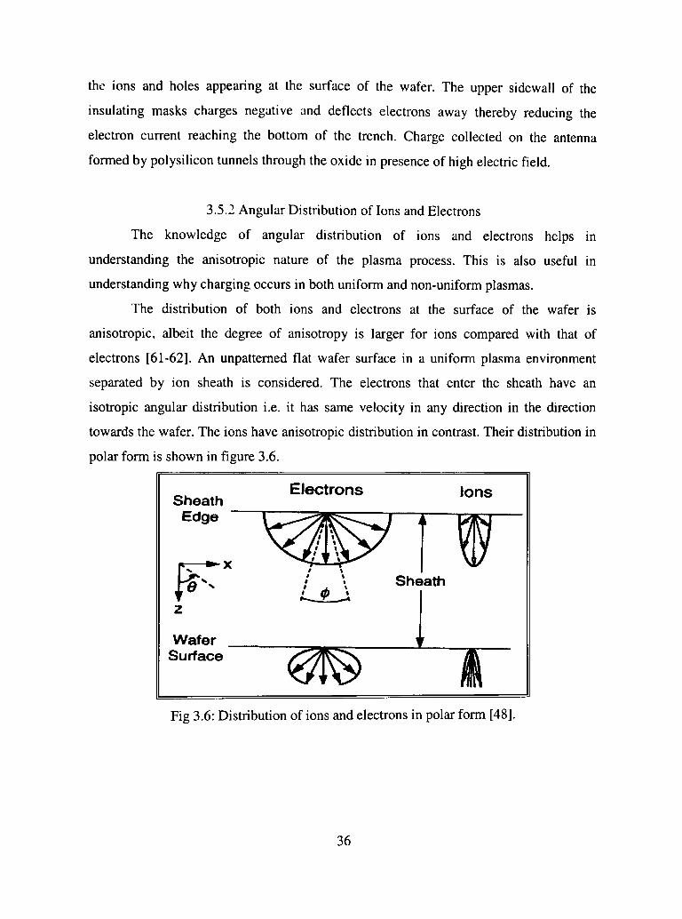
shown in figure 3.5. The cause for this is the inherent nature of the angular distribution of
35
the ions and holes appearing at the surface of the wafer. The upper sidewall of the
insulating masks charges negative and deflects electrons away thereby reducing the
electron current reaching the bottom of the trench. Charge collected on the antenna
formed by polysilicon tunnels through the oxide in presence of high electric field.
3.5.2 Angular Distribution of Ions and Electrons
The knowledge of angular distribution of ions and electrons helps in
understanding the anisotropic nature of the plasma process. This is also useful in
understanding why charging occurs in both uniform and non-uniform plasmas.
The distribution of both ions and electrons at the surface of the wafer is
anisotropic, albeit the degree of anisotropy is larger for ions compared with that of
electrons [61-62]. An unpattemed flat wafer surface in a uniform plasma environment
separated by ion sheath is considered. The electrons that enter the sheath have an
isotropic angular distribution i.e. it has same velocity in any direction in the direction
towards the wafer. The ions have anisotropic distribution in contrast. Their distribution in
polar form is shown in figure 3.6.
Sheath Edge
Electrons Ions
-^-^
Wafer Surface
Sheath
^ ^
Fig 3.6: Distribution of ions and electrons in polar form [48].
36

The ions entering the sheath are accelerated by Bohm velocity [63] in a direction
perpendicular to the wafer and is given by
Where, UB - the Bohm velocity
ks - the Boltzmann constant
Te - the electron temperature
Mi - the ion mass.
The velocity of the ions at the sheath edge in the parallel direction is given by [48],
" i M, Uii - the thermal velocity of ions in the parallel direction
T| - the ion temperature.
The ion velocity in the normal direction {u^ = UB) is larger than its thermal
velocity in a direction parallel to the wafer by a factor of 3 to 5 times in magnitude [63].
The acceleration of ions in the sheath results in the amplification due to the presence of
non-linear electric field that is time varying. This acceleration makes the ions highly
directional and their velocity at the surface in the perpendicular direction becomes 10 to
20 times that of MJ . The electrons on the other hand get decelerated in the positive sheath
as the wafer acts as the cathode terminal. Only a small fraction of electrons, whose
velocity component in the perpendicular direction when it enters the sheath satisfies the
condition below, reaches the wafer surface [48].
Where, M^ - normal velocity component of the electron
qe - the electron charge
Vdc - the minimum dc sheath potential
Me - the electron mass.
37

As the electrons approach the wafer, the angular distribution broadens and is
described by cos"0 where n < 1 and 0 is the angle of incidence of electrons at the wafer.
The angular distribution of ions and electrons and the ion energy distribution function
( I E D F ) are shown in the figure 3.7 and figure 3.8 respectively.
0.10 -
S a o li 3 ?
K
0.06 •
0.00
Angle, rad.
COS
Q
^ ' I p g a r j i n i | n f n n y i m m m i m i n t i , , , | i .
(b)
Q,QQ ^•'••^'•'•^••'•^-••'*-"'*-ffi- «
0 10 2 0 3 0 4 0 S 0 6 0 7 0 8 0
Energy (eV)
Figure 3.7: Angular distribution. Figure 3.8: Ion energy distribution function.
The figure 3.7 illustrates the results for typical conditions: electron density ne =
IxlO'"^ cm" , electron temperature Te = 4.0V, ion temperature Ti = 0.5V, wafer electrode
biased at co = 0.4MHz and peak-to-peak voltage Vpp = 60V. The ion angular distribution
shows bimodal distribution with two pronounced peaks close to the wafer normal. The
two lobes move closer with the reduction in the ion energy. The electron distribution has
a broad peak in the direction normal to the wafer. The following inferences can be made
from the discussion above.
a) Both ion and electron distribution are anisotropic at the surface of the wafer.
b) Flux of both ion and electron is highest in the direction normal to the wafer.
However the electron flux is lesser than the ion flux in the normal direction.
c) In steady state, the ion flux at any plane segment is equal to the electron flux at
the same segment as required to maintain current balance.
38

d) Most of the ions arrive at angles close to the normal incidence while majority of
the electrons impinge at angles that deviate significantly from the normal
incidence.
3.6 Gate Oxide Degradation
3.6.1 Charging in Non-Uniform Plasma
The surface of the wafer charges whenever there is an imbalance between the ion
and the electron current at the surface. This is illustrated with a simple doped Si wafer
covered with thin insulating layer exposed to plasma. A small segment at the center is
exposed directly to the plasma as shown in figure 3.9.
(a)
7^=0 v=o
J + i nJ-•r vv=o awg m»j»,ii>M »»,M»AtfMMJJUf/A
V sub
Substrate Potential. V
Fig 3.9: Relative flux of ions and electrons in non-uniform plasma [48].
The wafer potential is initially assumed to be at OV. The ion and electron fluxes
into the wafer are exacfly balanced. As the potential of the wafer is altered, an imbalance
is created between the ion and the electron fluxes. With the increase in the potential of
the wafer, more electrons are attracted and comparatively few ions are repelled due to
which the electron flux increases and the ion flux decreases. Net negative current flows
39

through the exposed area so that a balance in the ion and electron current is established.
Charging thus alters the electron and ion current arriving at the surface. The contrary is
also true wherein any imbalance between the ion and the electron current at the surface
results in its charging. If the ion flux is greater than that of electrons, then the surface
charges positively so that more electrons are attracted until the balance between the two
fluxes is established. The surface charges negatively if the electron flux is more than that
of ion flux.
3.6.2 Charging in Uniform Plasma
Electron Shading
In a uniform plasma environment, the ion and electron flux arriving at a planar
surface are equal. However, more ions arrive in a direction normal to the surface and
electrons arrive at oblique angles as shown in figure 3.10.
(a) J i
; t J .
^ 4 :-
A S
Figure 3.10: Electron shading in presence of pattern in uniform plasma [48].
In the presence of a pattern on the wafer such as a photoresist line, the ion flux is
not affected much as most of it is incident in the normal direction. From the figure 3.10
(b) it is apparent that the electron shading occurs thereby decreasing the net electrons
40

arriving at the surface. In the case of a conducting surface, the transportation of electrons
from other unshaded areas maintains the electron current balance. For an insulating
surface, the surface charges up positively thereby deflecting ions. With an increase in
potential, more electrons are attracted toward the surface and net electron current
increases. Charging of the surface continues till the increase in electron current
establishes a steady state.
The current imbalance becomes more severe whenever a trench is formed by two
photoresist lines close to each other as shown in figure 3.10 (c). Most of the ions still
reach bottom of the trench whereas the oblique electrons are shaded from both directions.
More charging has to occur on the surface so that the potential can raise higher compared
to single line pattern thereby deflecting most of the ions back to plasma on an insulating
surface. For a conducting surface, current balance is maintained by transportation of
electrons from other unshaded areas.
41

CHAPTER IV
EXPERIMENTAL APPROACH - CHARGE MONITORS
The latent nature plasma charging that results in the electrical degradation or
breakdown of thin gate oxides is aggravating requiring special on-wafer charging
monitors that can detect its occurrence and thereby preventing the further processing of
the damaged wafer. An ideal monitor should be able to determine device parameters most
sensitive to plasma damage - V,, gm, Idsat, Ig, etc., help determine at which process step
the plasma damage occurs and must be relevant to the real circuit performance and
reliability [64] . Sometimes the monitor should be able to catch those defective gate
oxides whose leakage currents are so small that they all pass the leakage fail criteria [65].
However a viable monitor is one that meets certain requirements like simplicity, cost,
testability, sensitivity and repeatability [66].
4.1 Monitors at the wafer fab
The main purpose of developing a monitor is to identify the single-bit fails in
EEPROMS. A monitor that can examine the charging effect of the tunnel oxide of the
EEPROM would be useful. However a more generic monitor would serve the purpose of
monitoring the gate oxide in addition to the tunnel oxide just by varying the process. The
two different types of monitors that were developed at the wafer fab by which the
charging of the oxide could be analyzed are
R2D2 Device-These are made up of antenna structures similar to the ones that are
very commonly used for monitoring purposes [64, 67-70]. A simple antenna structure
consists of thin gate oxide that is covered with a floating poly. The poly usually extends
over the field oxide thereby forming an antenna structure. The ratio of the area of the
poly to that of the tunnel oxide below is known as the antenna ratio. A number of square
block and finger structure antennas with antenna ratios varying from 37:1 to 54800:1 for
block antennas and the perimeter to area ratio from 13:1 to 41507:1 were used in the
monitor to characterize the tunnel oxide.
42

C3P0 Device-These were designed to make the monitors more relevant to the
actual EEPROM cell. These are made up of actual 2K memory cells that are connected
together and p type of MOS capacitors.
4.2 R2D2 Device
Antenna structure is the basic block used in this monitor. The figure 4.1 shows a
simple antenna structure.
BPSG (ILD) Poly Antenna Metal Bond Pad (optional)
Field/Thick Ox
Silicon
Tunnel Oxide (or gate)
Implant (optional)
Figure 4.1: Basic Antenna Structure [database].
The antenna structure consists of a thin gate oxide that is covered with poly on top
as illustrated in figure 4.1. The poly that covers the tunnel oxide extends over the field
oxide forming structures similar to antennas. The antenna ratio is defined as the ratio of
the total area of the poly on top to the area of the tunnel below. Different antenna ratios
can be obtained by varying the area of the poly and/or tunnel.
These structures are designed, in such a way to allow processing, using as simple
as 2 mask levels (Active and poly) or as robust as 9 levels. Different antenna structures
are obtained with different geometric configurations of polysilicon. The poly deposited
could be simple square blocks as shown in figure 4.2 or they may be finger structures as
shown in figure 4.3.
43

TUVMI Tunn*l
Figure 4.2: Poly with square blocks and finger structures [database].
Some of the other structures like Metal only pad-fingers and poly pad-fingers are
shown in the figure 4.3.
^ . - ' ^ - ^ ^ • ^ ^ .
Figure 4.3: Metal only pad with finger structure, finger and poly pad structure [database].
In addition to the shape, the size of these blocks may also be varied. Two blocks
of 50^m X 50|im and 100|im x lOO^m are used apart fi-om the lum cell. The thickness of
the finger structure is either 1.5 ^m or 2.5 |J,m.
Two parameters of primary importance in such structures are the Antenna ratio
and the perimeter to the area ratio. Antenna ratio for block structures is defined as the
ratio of the area of the entire poly block covering both the tunnel and the field oxide to
the area of the active gate (i.e. tunnel area). For finger structures, the ratio of perimeter of
44

poly fingers rather than their area, to the area of the tunnel is considered. The floating
polysilicon and the metal when exposed to plasma result in their charging and
subsequently this tunnel through the thin tunnel oxide at high fields. A wide range of
antenna ratios allows a wide range of testing to examine the effects of charging on the
tunnel oxide. Table 4.1 lists various antenna ratios that were designed at the wafer fab.
Tox size (urn)
0.5 0.6 07 0.8 0.9 1
1.1 1.2 1.3 1.4 1.5 1.6 1.7 1.8 2
Tox area (um*um)
- -
0.25 0.36 0.49 0.64 0.81
1 1.21 1.44 1.69 1.96 2.25 2.56 2.89 3.24 4
lum cell
15712 10911 8016 6138 4849 3928 3246 2728 2324 2004 1746 1534 1359 1212 982
Antenna Ratio ^ ^ H ^ ^ B B
50*50 Block
24823 17238 12665 9697 7661 6205 5129 4310 3672 3166 2758 2424 2147 1915 1651
100*100 Block
54823 38072 27971 21415 16921 13706 11327 9518 8110 6993 6091 5354 4742 4230 3426
Table 4.1: Antenna Ratios [database].
For similar antennas, different antenna ratios are obtained by keeping the area of
the poly fixed and by varying the area of the tunnel. Conventional antenna structures
have fixed active dimension (minimum size) and varying poly area [64]. However the
advantage of keeping the poly area fixed and varying only the active area is that it is
possible to find out if the damage is due to plasma charging or if it is due to process
induced defects. This can be found by comparing the leakage current of larger active
areas (i.e. smaller antenna ratios) with that of smaller ones. In case of process induced
random defects, active area having larger area would show more leakage than the smaller
active areas as they will be affected most.
45

4.3 Process Flow
The antenna structures illustrated above can be realized in two ways which results
in two different process flows. The two process flows differ in the way in which active
area (i.e. the tunnel area) is defined.
4.3.1 Active Flow
This is similar to the conventional flow in which the active is defined by growing
the field oxide first. The tunnel oxide of thickness 10 nm is then grown. The poly is then
deposited and implanted/ deposited with phosphorous. The poly mask then defines the
area of the floating gate. The design can be kept simple by limiting it to only two mask
levels namely the Active and the Poly. However additional optional mask levels can be
included such as initial implant, contact implant for creating ohmic contact to the bond
pad, contact and metal depending on the complexity of the flow. Thus the number of
mask levels could range anywhere from 2 to 6 levels.
4.3.2 Inverse Active Flow
In this flow a thick oxide is first grown on the entire wafer. A mask is then used to
define the tunnel area where the thick oxide is etched back to the substrate. This is called
the inverse active flow because rather than the field oxide defining the active area, a
separate mask is used to do so. This was done for two reasons: the flow was shorter and
hence the wafers could be processed much faster compared to the active flow in which
the field oxide growth defines the active area; another important reason being any
physical stress on the tunnel oxide due to encroachment of birds beak into the active
region could be eliminated by growing a thick oxide first and then etching them back to
silicon to define the tunnel region.
46

Table 4.2 shows the skeleton flow for both Active and Inverse Active processing.
Active Flow
Initial Implant (Optional) Active Patterning through standard field
oxide growth Tunnel Oxide growth
Poly Deposition Phosphorus Implant/Deposition
Poly Patterning BPSG Deposition and Densification
Contact (Optional) Metal (Optional)
H2Bake
Inverse Active Flow
Initial Implant (Optional) Thick oxide growth followed by etch back to substrate to define the active
Tunnel Oxide growth Poly Deposition
Phosphorus Implant/Deposition Poly Patterning
BPSG Deposition and Densification Contact (Optional) Metal (Optional)
H2 Bake Table 4.2: Active and inverse active process flow [database].
The processing of EEPROMS involves numerous plasma enhanced chemical
vapor deposition and etching steps which can cause cumulative charge damage of the
tunnel and gate oxide [71, 72]. It is necessary to monitor the antenna structures after
different plasma processing stages. It has been reported that as the polysilicon conductor
lines are not typically wired to protection diodes until the first level of metallization, gate
oxide charge damage from process prior to metallization can be significant. The gate
oxide damage due to plasma deposition of PSG has also been identified [73]. As a result
it becomes necessary to evaluate the charging after each plasma processing stage that is
known to cause the oxide damage. Another commonly used practice in plasma processing
of insulated films is the use of power-lifting technique. The residual charges on the film
are neutralized with low-power plasma at the end while unloading them. This is done to
prevent unexpected movement of the wafers due to electrostatic force which might result
in the crashing of the wafers during unloading. The plasma-assisted wafer de-chucking
step has also been reported to cause significant damage [74, 75]. As a result some of the
wafers are split and processed without power-lifting to see if there is any improvement
over the others.
47

4.4 C3P0 Device
The antenna structure in the R2D2 monitor has the advantage of being a simple
structure which can be used to evaluate the effect of charging in plasma. The antennas
can be made highly sensitive since the charge-collecting capabilities depend on the size
of the floating structures and larger the size of antenna more sensitive will it be to
charging. But some of the high antenna ratios used to induce plasma damage is done
merely for plasma damage studies and not for plasma damage assessment in
manufacturing. C3PO monitor is designed such that the test structure correlates with the
actual circuit component. The two structures used in this monitor are
a) PMOS Capacitors (CAPA2P)
b) EEPROM Cell (EPRM)
4.4.1 CAPA2P Device
The usage of PMOS transistors as a monitor has also been widely reported [65,
76, 77]. The test structure imitates a PMOS transistor with the gate pad acting as a charge
collecting antenna. Prior work at the wafer fab has shown PMOS transistors to be more
sensitive to plasma damage (both random area defects and charging damage) over NMOS
transistors [77]. This monitor will therefore incorporate only the PMOS structures as
shown in the figure 4.4.
Figure 4.4: Cross-section of CAPA device [database].
48

The MOS Capacitors were fabricated, with a tunnel oxide and a polysilicon gate
thickness of lOnm and 430nm respectively, using the standard CMOS lum process. A
blanket N-well was first implanted on the wafer followed by the other processing steps.
Six such capacitors (PI to P6) are used with the antenna ratio between 1.0-1.5 for five of
them (P2 to P6) and an antenna ratio close to 100 for the other (PI).
Process Flow
This is similar to a conventional PMOS flow but with a blanket n-well implant
done instead of patterning the n-well. The active pattern then defines the field oxide
region. A tunnel oxide of 10 nm is then deposited followed with poly and phosphorus
deposition. NSD and PSD implant is done after patterning the poly. The final two masks
contact and metal complete the flow. Table 4.3 shows the skeleton flow for the CAPA2P
structures.
CAPA2P Flow
Initial Clean and Pad oxide Blanket n-well implant
Active Patterning through standard field oxide growth Tunnel Oxide Growth
Poly Deposition Phosphorus Deposition / Implant
Poly Patterning NSD Pattern
NSD Implant and Anneal PSD Pattern PSD Implant
BPSG Deposition and Densification Contact Metal
IVIask Levels
1
2 3
4
5 6
Table 4.3: Skeleton process flow for CAPA2P device [database].
49

4.4.2 EPRM Device
EEPROM based sensors has been used in some of the recent work to examine the
interactions between the wafer and its environment. These sensors have been used to
quantify the UV and charging characteristics of different process tools [78-80]. A
monitor similar to the EEPROM cell in the fab has been designed to study the effect of
charging on the tunnel oxide.
The basic memory cell has been modified as little as possible to change it into a
monitor. The select transistor has been removed as it is used only for addressing
purposes. The floating gate has been brought out through a separate contact so that the
tunnel oxide can be tested independently. Figure 4.5 illustrates an EPRM structure.
Control gate
Floating gate
Dnin
Floating gate
Control gate
Ccg -
'
1 1
MM1
•
MM3 • •
J L
Ccg -
'
.. 1 Source
Source
Ccg :
<
1 1
M M 2
<
MM4
1 1
Ccg -
r L r •
Floating gate
Drain
Floating gate
Figure 4.5: Schematic of EPRM device.
Process Flow
The process flow for the EPRM monitor is similar to that of the EEPROM cell.
The field oxide defines the active region. The depletion mask is then used to define the
depletion capacitor for the cell. The gate oxide is then grown and a tunnel window is
etched in which a thin tunnel oxide of 10 nm is grown. This is followed by Poly, Contact
and the Metal mask.
50

Table 4.4 illustrates the skeleton flow for EPRM monitor.
EPRM Flow
Initial Clean and Pad oxide Active Patterning through standard field oxide growth
Depletion Pattern Depletion Implant and Anneal
Gate Oxide Growth Tunnel Oxide Pattern
Poly Deposition Phosphorus Deposition / Implant
Poly Pattern BPSG Deposition and Densification
Contact Pattern Metal Pattern
Mask Level
1 2
3
4
5 6
Table 4.4: Skeleton process flow for EPRM device [database]
Another modification done in the monitor for faster testing of the cells is that all
the cells in one die have been connected together in parallel. Since the EEPROM has 2Kb
size, the floating gate of all the 2K cells have been connected together.
4.5 Testing Methodologies
The Plasma-induced charge damage to thin oxides includes excessive leakage
current, early breakdowns, increase in surface, bulk and interface defects, and a decrease
in the charge-to-breakdown value. Some of the methods available for testing include
a) Ramp Voltage Stress
This is a destructive way of testing the gate oxide. Intrinsic breakdown of the
oxide refers to the breakdown of capacitor whose field is much above 10 MV/cm. If the
breakdown occurs much before the field across the oxide reaches this value then it
referred to as early breakdown. Control wafers without any plasma processing show
purely intrinsic breakdown. Some of the oxides that are exposed to the plasma show early
breakdown. The percentage of early breakdown device increase with increasing antenna
sizes as larger antennas are more susceptible to plasma damage. A typical graph shows
51

the variation of percentage cumulative failure with the Breakdown voltage. This may not
work if the plasma stressing is not severe.
b) Capacitance-Voltage measurement (C-V)
This is a nondestructive way of testing the oxides. This test is highly sensitive to
thin oxides that have large area. A shift or distortion is noticed in the C-V curves of the
damaged oxide when compared to that of control wafers. Since this is not destructive, a
single site on the wafer can be tested after different stages of processing. The defects that
can be studied using this test include 1. interface states at Si/Si02 interface Djt, 2. fixed
oxide charge at the Si/Si02 interface Qf, 3. charge trapped in the bulk of oxide Qot, and 4.
mobile ionic charges Qm. A typical graph shows the variation of the Capacitance of the
MOS as the gate voltage is varied from a negative voltage to a positive voltage.
c) Current-Voltage measurement (I-V)
The thin oxide is tested by F-N tunneling current. The gate leakage current is
measured as the gate voltage is varied from 0 to a high value. A typical F-N plot is
constructed which shows the variation of In (J/E^ox) with l/Eox- However along with the
flat band voltage, the surface band bending (during accumulation) and the surface
potential (during inversion) has to be considered while calculating the field across the
oxide.
d) Time Dependent Dielectric Breakdown (TDDB)
Qbd tests are very sensitive to more subtle oxide damage which affects the long
term reliability of the oxide. The fast ramp voltage tests are sensitive to more
catastrophically damaged oxides. Qbd tests also have an advantage of being repeatable
incase of intrinsic breakdown.
The ramp voltage stress using bench tester and step voltage using automated tester
is used for evaluating the leakage characteristics of tunnel oxide because of simplicity of
the test and the time involved.
52

CHAPTER V
RESULTS AND DISCUSSION
Three batches of wafers with thirty three wafers were processed for a
comprehensive analysis of charge damage. Such a high number of wafers were due to the
fact that the number of variables on which the charging would depend was quite a big set.
The following are some of the variable parameters whose influence on charging was
evaluated.
a) Control Wafer-This did not receive any BPSG on it.
b) BPSG Deposition-Five machines Ml, M2, M3, M4 and M5 were used for BPSG
deposition. The number of wafers increased as the four process tools had to be
evaluated for charging damage of the tunnel oxide.
c) Power-Lift-This is the standard recipe that is used in the BPSG machines in which
low power plasma is used, while unloading, to neutralize charges which may
otherwise result in crashing of wafers due to electrostatic force [81]. As this method
had been reported to cause damage to the oxide some of the wafers were split from
the main lot so that they did not receive any power-lifting.
d) Processing Steps-Since it is necessary to evaluate the charging after each plasma step
that is suspected to cause damage to the oxide, different wafers were stopped at
various stages in the flow. Some of the wafers were probed before BPSG, some after
contact etch and the others after the metal etch.
e) NSD Implant-The NSD Implant, used in the standard EEPROM flow, is done after
the polyoxide growth and ILD step. This high energy implant may exacerbate any
problem in the BPSG process. Some of the lots add steps to match standard process
flow, used for EEPROM, through N-i- Source Drain Implant.
f) Variations across the wafer-The testing had to be performed at various places across
the wafer to see if the damaged oxides had any relation to their location.
53

5.1 First batch
The first batch o\ wafers was processed which had three wafers. To verify the
initial assumption made m the hypothesis that plasma processing could be the responsible
for the damaged oxide, a control walci was processed only till the polyetch. If the
leakage current measured on this wafer is below the threshold value o n ^ A even at fields
beyond 10 MV cm then it is reasonable to assume that the oxide is of good quality until
then in the flow. The second wafer received further processing and received a BPSG
deposition and densification. The BPSG thus deposited was stripped off using wet etch.
The third wafer went on till it received metal deposition and patterning. If the leakage
current measured on these two wafers crosses the threshold value before the field across
tunnel reaches 10 MV/cm, then one can conclude that the damage to the oxide occurred
after the poly etch step. Table 5.1 shows special work request (SWR) for the first batch.
R2D2 Lot No
A1
A2
Wafer No
1
2 3
Poly pads Metal
Comments
No BPSG
Process in Ml -STD Recipe Process in M3 -STD Recipe
Table 5.1: Wafer split for first batch.
These wafers were stressed using a voltage ramp from 0 to 15 volts in the
accumulation mode. They were bench tested on Keithley 4200. The variation of the
leakage current for three wafers from the first batch is shown in the figure 5.1.
W a f e r 01 rJo i i B P S G W a f e r 02 : r,11 B R S G S w i p o f t W a f e r 03 fwU B P S G a n d M e t o l
R 2 D 2 l _ o a k a g e O u r r e n t B a t c h 1 - L o t A 1 . A 2
W a f e r s 0 1 , 02 . 03
- AR = i 6 < i a i - V./F1 - A.R = 1(5921 - •A'F2 A R = 1692 1 - ',--'F3
W a f e r 0:i : M 3 B P S G a n d M e t a l
Apffltad Vnltoa"
Figure 5.1: Leakage current for wafers fi-om first batch.
54
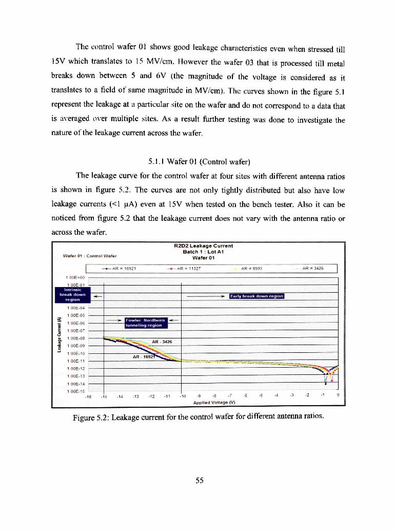
The control wafer 01 shows good leakage characteristics even when stressed fill
15V which translates to 15 MV/cm. However the wafer 03 that is processed till metal
breaks down between 5 and 6V (the magnitude of the voltage is considered as it
translates to a field of same magnitude in MV/cm). The curves shown in the figure 5.1
represent the leakage at a particular site on the wafer and do not correspond to a data that
is averaged over multiple sites. As a result further testing was done to investigate the
nature of the leakage current across the wafer.
5.1.1 Wafer 01 (Control wafer)
The leakage curve for the control wafer at four sites with different antenna ratios
is shovra in figure 5.2. The curves are not only tightly distributed but also have low
leakage currents (<1 |iA) even at 15V when tested on the bench tester. Also it can be
noticed fi"om figure 5.2 that the leakage current does not vary with the antenna ratio or
across the wafer.
Wafer 01 ; Control Wafer
R2D2 Leakage Current Batch 1 : Lot A1
Wafer 01
- R = 1132^
•S 1
- • 1
1
1
1
1
1
OOE-CU
OCE-05
OOE-06
OOE-ilT
OOE-03
0CE-C9
OOE-IO
OOE-11
OOE-12
OOE-13
O O E - U
OOE-15
Fowler- Nofuhei i lunr>eling region
Bunsazmisiai
•-""' ^ =;;rv?i 5^^i-
• 10 -9 -3 -7 -6
Appl ied Voltage (V)
Figure 5.2: Leakage current for the control wafer for different antenna ratios.
55

Depending on where the tunnel oxide breaks down three regions can be defined.
a) Early Breakdown Region: The F-N tunneling is known to occur around lOMV/ cm
and it is desirable that no site break down before the tunneling phenomenon takes
place. So this region is called the Eady Breakdown Region.
b) Fowler-Nordheim Tunneling Region: Once the field across the tunnel oxide
reacheslOMV/ cm or greater, the tunneling is known to occur. The memory cells are
subjected to this field during write and erase operation. From figure 5.2 for the
control wafer, the F-N tunneling is seen to occur beyond lOV till 15V. This region is
called the F-N Tunneling Region.
c) Intrinsic Breakdown Region: The sites on the control wafer were stressed beyond
15V and irreversible breakdown (a sudden drop in the dc resistance) were noticed
between 15 and 17V. As a result, this region is called as Intrinsic Breakdown Region.
All the sites on the control wafer were stressed till 15V and the irreversible
breakdown was not noticed. To estimate the magnitude of the voltage at which this
breakdown occurs six sites were stressed beyond 15V. The histogram can be seen in the
section 5.5.2 on quantitative analysis. The breakdown voltage for these sites ranged from
15V to 17V with an average breakdown voltage of 15.95V and a standard deviation (SD)
of 0.497V.
5.1.2 Wafer 02 (Machine 1 BPSG followed with strip off)
The breakdown voltage was either the voltage at which the sites would
irreversibly breakdown or the voltage at which the current through the antenna structure
reached l^iA depending on whichever occurred eariier. The sites stressed on wafer 02
show a bi-modal distribution of the breakdown voltage. Some of the sites tested
breakdown between 6V and 12V (average of 9.6V and SD of 1.33) in the early and the
Fowler-Nordheim tunneling region while the others between 15V and 17V (average of
15.8V and SD of 0.368V) in the intrinsic breakdown region. The histogram in the on
56

section 5.5.2 on quantitative analysis shows their distribution. The sites that show
intiinsic breakdown have excellent quality of oxide whereas those sites that breakdown in
the other two regions are degraded and such of those sites that appear in the memory cell
make them leaky as they can not sustain high programming fields.
5.1.3 Wafer 03 (Machine 3 BPSG and Metal processing)
Sites with lOOfxm ^ 100|am poly blocks having different antenna ratios were
sti-essed using a voltage ramp ft-om 0 to 15V. Figure 5.3 illustrates the leakage current for
the wafer 03.
W a f e r 03 . B P S G ( M a c t i l n e 3 > j n d M e t a l
R 2 0 2 Leakage Current Batch 1 : Lot A2
Wafer 03
A R = B 1 1 0
I 0O€-0Q
1 CCE-C'
^
liJIIUI.llJlUll.ll.NJI|.J.IIJI.I
A R - 16921
tJ.VM.\U.t\.UlUM.t-
'^?f:r'
Applied voltage (V>
Figure 5.3: Dependence of leakage current for wafer 03 on antenna ratio.
An important observation that can be made fi-om the above graph is that higher
leakage current and/or faster breakdown is noticed with increasing values of antenna
ratios. This is in accordance with the well known theory that the charging is proportional
to the area of the floating gate [64, 78, 48]. This will help us in identifying the source of
damage to the tunnel oxide.
From the above graphs and analysis it is evident that the confi-ol wafer which is
processed till poly etch has oxide of good quality as all the sites tested breakdown beyond
15 V. As the breakdown is noticed in the early and the F-N tunneling region for the other
57
two wafers that receive BPSG it can be concluded that the oxide is getting degraded
because of the damage that occurs beyond the poly etch step. As plasma is used for
BPSG and is known to cause Gate Oxide Integrity (GOI) problems one can, at this stage,
attiibute the tunnel oxide degradation to the plasma processing as suspected in the
hypothesis. However the damage to the tunnel oxide could be due to the defects induced
in the oxide and/or on the substrate, or because of the charging in the plasma
environment.
The design of the antenna structure helps us to differentiate between the defect
induced damage and the damage due to the charging of the oxide. Different antenna
ratios were obtained by varying the area of the tunnel below the antenna and by keeping
the area of the poly on top fixed. If the oxide was degraded due to the defects then the
leakage current should have reduced with increasing values of AR and the opposite trend
should have been seen in the figure 5.3. If the damage is due to charging of the oxide,
then according to the model developed in section 6.1 on physical model, leakage current
should be directly related to antenna ratio as is seen in figure 5.3. Thus it can be
concluded that the gate oxide degradation is due to charging of the oxide during plasma
processing and not due to the defects.
Relation between charging and antenna ratio
Increasing leakage current and/or faster breakdown was noticed in the figure 5.3.
We now try to establish a relationship between the breakdown voltage of the antenna and
the antenna ratio. As seen in the quantitative analysis section the breakdown voltage
reduces with increasing AR. We try to find the best fit with a minimum of two free
parameters. The coefficient of determination (r) for linear fit has the value closest to one
(0.98) compared to all other fits with two free parameters (exponential, logarithmic,
power). Hence a linear relationship is noticed between the breakdown voltage and the AR
for the wafer 03.
A similar fit is tried for the breakdown voltage of wafer 02. However some
outliers are seen for this wafer. This could be due to the non uniformities in plasma.
58

5.2 Second Batch
This batch of wafers was processed to study the effect of power lifting on the
charging of the oxide and to estimate the yield for different antenna ratios. Table 5.2
shows the SWR for the second batch.
R2D5TP^
— - -
L o t N o
t31
0 2
B 3
W a f e r N o
_ 10
2 3 4 5
6 7 8 9
11 1 2 13 14
15 16 17 18
R2D2
Metal Metal Metal Metal
Metal Metal Metal Metal
Poly pads Poly pads Poly pads Poly pads
Poly pads Poly pads Poly pads Poly pads
CoiTi m e n l A H l i H H l i i M ^ i i i | | M | | ^ ^
Note wafers 1 and 10 will not have BPSG Dep.
Process In M4 -STD Recipe Process in M5 -STD Recipe Process in M2 -STD Recipe Process in M3 -STD Recif>e
Process in M4 -without powerlifl Process in M5 -virithout powerlift Process in M2 -without powerlift Process in M3 -without powerlift
Process in M4 -STD Recipe Process in M5 -STD Recipve Process in M2 -STD Recipe Process in M3 -STD ReciF>e
Process in M4 -without powerlift Process in M5 -without powerlift Process in M2 -without powerlift Process in M3 -without powerlift
Table 5.2: Wafer split for second batch.
These wafers were tested on an automated tester (RI40) using step voltages from
6V to 12V in steps of 2V. As many as 30 sites were tested on each of the wafer. To study
the dependence of yield on the antenna ratio three different antenna ratios that were used
for testing are 21415, 9697 and 6138.
59

R 2 0 2 L e a k a g e C u r r e n t AR - 613B
M3
VVT 1 4 STD Rpc ipo WT 1 e WKtloul PowvIliK
','* ».'' s'' - ' ' ..'' J^ •••v- •:\- -.'i ..V • • v . ' ' . v . * '\-^\^\:.'-\:^\-\.^-\y-..'^-
!• rrrnHnrvfrrTTtfirrr* mown K n tvi m> rtrrrn > m
Mot Arr-.>\
M5 M2 M4
Wt 12 STDReripo Wl 16 Without Powerlift wr I 3 STO Recipe
Wt 19 Without Powerlin W t l S STO Recil..?
fg^y'gfg^ i^f^y^jfT' y ^
Figure 5.4: Leakage current for an antenna ratio of 6138.
R202 Leakage Current AR9697
. K . S , S ' , 1 - .; .- .^ l - •V' .V. ,|V.. ._> . - S , j ^ .'• ^\ ,'^ ,tr. ,t-. , t ,
1 OOE 04
I OOE-05
1 OOE-06
1 rioe 0 7
S I ijfiE-riy
t 1 rjuE-09
1 OOE 10
1 UU6-11
1 o o E - i :
1 OOE-1 3
• iniRIIIIIIIIIIIMIIIIIU • ••iiiJRiBiiiiiiiiiai • ••iimpiniHiiuiiiiiniiaiiii
M3 w n 4 STOR«?cipe WT 1 8 Wilhoul Powerlifl
^i .aiK,.^lL_r.
M5 M2 M4
w r i 2 STORetipe Vvn6 'ViithoutPowerlitl
— F-v> A,^ , U WT 1 -.1 ^' ic- rrpcipe SVtl9 WilhoutPowerlin
V,ff i5 STDRet ioe
y*^^t<^v ^ ^ j
Figure 5.5: Leakage current for an antenna ratio of 9697.
60

R202 Leakage Current AR - 21415
»^ . ' M I S H
«>. . 1 - .h . 1 . ,« .«. . « . " -•l / l ' ' / l ' A .te ' .b ' " .•> . ' s * /:,*• / ! > , . ( " , ^ ' ' , , J
I] ' .".t Ll.f 9.t.^
.y> fi-j .<o
M3 WI14 STDR«ip» Wl 18 Without Powwiim
M5 M2 M4 ~,
w t i ; STO Recipe-wr 16 Without Pcwerlift
w n 3 STORocipe wr 19 WithoutPowertifl
_K M^H^ Tlcr U^\
f'-^.j i'-'''1. %.< i' ^^ I ' T
:?i^
w r i s STDRecipej
Nf—MfrrS
-f^-fs^l^L^Si^s^ ij n Figure 5.6: Leakage current for an antenna ratio of 21415.
From figure 5.4, 5.5 and 5.6, the leakage current can be seen increasing with the
applied voltage for all the wafers. The number of sites, for wafer 14, that breakdown at
12V is 1, 2 and 9 out of 30 sites tested for an AR of 6138, 9697 and 21415 respectively.
Thus number of sites breaking down is directly related to the AR. This is similar to the
trend of leakage current increasing with AR seen in the first batch of wafers. As the
sensitivity to charging increases with the AR, square blocks with highest AR of 21415
were most commonly used for testing. Wafers that received BPSG fi-om M3 had the most
damage.
Some of the wafers fi-om the lot Bl and B2 were then tested on the bench tester
and the leakage curves obtained is as shown in figure 5.7. Wafer 10 which is the control
wafer, wafer 07 that received BPSG fi-om M5 with metal processing and wafer 09 that
received BPSG fi-om M3 along with metal processing were stressed using a ramp voltage.
61

WAfei 10 Control w.sti*i Wafei 0? M5 without Powwillh * M»t.sl War»i 09 M3 without Powi»illh > Metcil
R 2 D 2 L e a k a g e C u r r e n t B a t c l i 0 2 ; L o t B 1 . B 2
W a f e r s 0 7 . 0 9 . 10
100E»00
1 OOE 01
1 OOE02
1 OOE-0 3
1 OOE-04
1 OOE O-i
S. 1 OOE-Or.
1 1 OOE-0'
3 1 OOE 03
S 1 OOE-09
3 1 OOE 10
1 OOE-1 1
WKfet or Uli liigh leakage cuirenl o l j j A i geen^l Ijefore intrinsic hreakdo^.n J
applied Voltage (V)
Figure 5.7: Leakage current for wafers fi-om second batch on test bench.
The wafer 07 that was processed through M5 showed higher leakage current and
faster breakdown. This may be due to the cumulative effect by which the tunnel oxide
that was damaged during BPSG was further degraded because of the metal processing.
This lot was scrapped due to mis-processing before fiirther test could be done on this lot.
The lot B3 that was tested using the automated tester was processed through BPSG
machines had poly pads on them for testing as they were not passed through metal.
Figure 5.8 illustrates the leakage for this lot.
• if-T i : :r-"cc5?sc-virhcut ? c " *fUr> - ^..'.-i'.Zl
I ^ — ' ' I t t e V = -Hi /
S c r i b e « : 3 1 6 ^ 4 2 -
A R = 2 1 4 1 S G a t e V = 6 . 8 , 1 0 ^ 1 2 - - I ' - j i f v ^ - & v • : -lit',- - ^ »
Morf number of sits* breaking do\T-ni--lLLAi
before incrinsic field
- , - "^' < i ' ' S ' <-.' - . " ' N ' *••*' • » ' ' >* ' V* "* -5:..- - ^ ' . . - - ' - , - - ' -.^*' - . ' " ' -,'^>' -."-' v't . ' *,"-' 'S^' •>*
M 2 M3 _2
'•.^'afer number
Figure 5.8: Leakage current for wafers form second batch on auto tester.
62

Extensive testing was done on this lot for three different AR (6138, 9697 and
21415) and all the reading obtained support the figure 5.8 in which more fails were
noticed for the wafer processed through M3 than any other BPSG machines. This was in
accordance with most of the earlier tests on first batch of wafers in which maximum
damage to the wafer passed through M3 was noticed. The yield information is extracted
and presented in section 5.5.2 on quantitative analysis. None of the graphs from batch
two show an improvement in the leakage current when power lifting technique is not
used. Both standard recipe and the wafers without power lift show similar leakage
current.
5.3 Third Batch
The inverse active flow was used to process these wafers in which a thick oxide
was grown and was etched back to silicon to define the tunnel region. Two control wafers
were processed one with NSD implant after the poly and the other without the implant.
To expedite the testing, automated tester was used.
The wafer splits fir this batch is shown in the table 5.3.
Splits for r-tirrnrfltil iMWillli irt^ iBilit • n
NSD Implant
BPSG Process
Metallization
Wafers
Implant at NSD No Implant
No BPSG MA M5 M 2 M3 M4 - without power lift M5 - without power lift M2 - without pwjwer lift M3 - without power lift
Contact etch only Contact and Metal
1
X
X
2
X
X
3
X
X
4
X
X
5
X
X
6
X
—
7
X
"" " 1
i
X X
8
X
' - -
X
9
X
X
10
X
X
11
X
X
X
1?
X
X
X
Table 5.3: Wafer spht for third batch.
63

These wafers were tested on the automated tester using step voltages fi-om 6V to
12V in steps of 2V. Figure 5.9 illustrates the leakage current obtained for the wafers from
third batch.
M 2 0 i L o n k o a e C u r r e n t
W f B 1 12 A R - 3 1 4 1 6
- O aTf» V p 6V.' -rttt^ V I :•-
I OOE: - 1 ; * 1 oriF -1 I oot-1
| N S O implant WfT 2 MV/D P-Owerlift VW 8 ^•^/o Po-^vrtm w r i o
Figure 5.9: Leakage for wafers from third batch with pin 16 as substrate connection.
The automated tester reading showed no variation in the leakage current for
different gate voltages. After a detailed inspection and some testing on the test bench it
was found that the wafers on the test bench used the back end of the wafer as a
connection to the substrate. Figure 5.10 illustrates the leakage current for one particular
site with pin 16 used as the cormection to the substrate and the backend of the wafer as
the substrate cormection in the other case.
R 2 D 2 Leakage C u r r e n t XA/afer 02 - Ar 21416
C o m p a r i s o n b/n Substrate and pin 16
- AR Z-;415 - sub •-— •„'..': 02 - A.R 2-'4-! 5 - pir
Applle<l Voltaoe
Figure 5.10: Leakage current with backend of the wafer as substrate cormection.
64

Figure 5.11 illustrates the leakage current for the same lot on the automated tester
with backend of the wafer as the substrate connection. Variation in the leakage current
with voltage was noticed but no difference was seen among the BPSG machines used.
R 2D 2 Invei- ie Act ive Leakage curi-ents
Wafe r 1-12 AR = 21416
M4 M5 M2
M3
Wt 3 -r- =!^-.-^ VVf i 5 t : R s ; c E vvf 5 S r : P 5 ; : i "Vf 6 S! :R=;c5 Wf 11 C:-B-,tEr;'-
imF -Tf l i - . **i^ f ^ v ^ - j t^-;;
Wt IZ C : - » ; t i - ^ # i NSC l"C3'tV^/f • i j
, r d i Figure 5.11: Leakage for wafers fi-om 3' batch with backend of wafer as substrate cormection
5.4 Comparison between Testers
The leakage current measured is highly dependent on the way the measurement is
done. To compare the leakage current obtained through different testers one of the wafers
was subjected to both ramp and step voltages. The sweep curves were obtained by
varying the voltage form 0 to -15 in steps of -O.IV using Keithley and HP tester. The
RI40 on the other hand uses step voltage starting at -4V and increasing it in steps of-2V.
Measurement was also performed using the same steps on Keithley tester. Thus the
following four combinations of test were possible.
a) Keithley sweep
b) HP sweep
c) RI step
d) Keithley step
65

0
1
0 3E-0S
0OE-J3
OOE '0
OOE ' *
O O E - • ;
OOE- • :
OOE- •'.
1 — • f ' ?
C omp xrlioii t} ii i»MU*Q» ourvt iVaUr 0 1 AR - 2 1d10
• • - » . i » j • ^ i J - i - - t
i
•fi :t
-'. : - : -5 . it z ZJ
• 1
& ^
Ik
' -- - : ^ - ^ — - ' ' . ' - ' • •
' • '
\ ' • ' " " ' • • ' • '
Keahtoy t»«t*r - Sweep ^
OB e z't»g»
Figure 5.12: Leakage current measured on Keithley, HP and R140 tester for wafer 01.
Comparison b'n leakage curves Wafer: 03 , AR =21415
-.3«"lay-3.veec h-5Jtfl-=y -atac
Keithley t e s t e r - S w e e p
0 0=-
• 3 3E-
OOE-
• O D E - '
• O O E -
Hp loster Sweefj
s -_JiL40_teslfi£-—-
\ V \ -^A^tv*^'^**^''***^***^*^*^'***'****^''''^^'''^^*^^
Gate Volta ge
Figure 5.13: Leakage current measured on Keithley, HP and R140 tester for wafer 03.
Form figure 5.12 and figure 5.13, it can be seen that the sensitivity of R140 and
the HP tester is very limited while measuring low leakage currents. At higher leakage
currents the readings from HP and Keithley match closely for a sweep voltage. Since the
66

Keithley had the best sensitivity for both lower and for higher currents it was concluded
that the above tests on Keithley yielded good results thus validating the results that were
obtained using sweep voltage on all the batches.
The final set of testing for the wafers form third batch was done on Keithley. With
the previous analysis it was noticed that the wafers processed through M3 and/or Metal
processing should have the maximum damage to the oxide compared to the others.
Supporting results were obtained from the final set of testing presented next.
R2D2 Leakage Current Batch 03; AR 21415
Wafer 01, 03,04,05,07,08,09 -Wf1 - AR = 21416 - W f 7 AR = 21415
-Wf 3 -AR = 21416 - W ( 8 AR = 21415
W f 4 - A R = 21416 W f 9 A R = 21416
W f 5 - A R = 21416
1 OOE-12
1 OOE-13
1 OOE-14
1 OOE-15
1 OOE-16
1 OOE-17
-^t- VW 1 ! M2 . We DP5G— - ^ Wf 4 - M5 - Std Recioe ^ .,iniiii»iMfcM,*wwi»<nniM*<>M* i<>*»***"***<i" i vsi*\*w%».v»»v*>w>»<'./' ^w. ^ A ^ ."
Wf 5 : M2 - Std Recipe
Wf 3 : M4 • Std Recipe
Applied Voltage
Figure 5.14: Leakage current measured on Keithley for lot that did not go through M3.
The leakage current for all the wafers that did not receive BPSG in M3 and which
have not been processed through contact and metal etches is illustrated in figure 5.14.
Lower leakage current is noticed for these wafers. With a threshold limit of 1 \iA none of
these wafers breakdown till 15V indicating that they all lie in the intrinsic breakdown
region. However the wafers that have passed through BPSG processing show higher
leakage currents compared to control wafers. Figure 5.15 illustrates leakage curves for
the wafers that are processed through M3 or contact and metal etch. Higher leakage
current and early breakdown can be noticed in these wafers.
67

K2D2 Leakage Current Batch 03 ; AR 21416 Wafer* 2,6,10,11,12
Applied Voltage
Figure 5.15: Leakage current measured on Keithley for the lot that went through M3.
The leakage current for all the wafers from third batch is illustrated in Figure 5.16.
Figure 5.16: Leakage current for wafers from third batch measured on Keithley.
68

It can be concluded that, from figure 5.16, the wafers that receive BPSG from M3
show maximum degradation of the tunnel oxide. This trend was noticed in the wafers
from batch one and two also. The susceptors in this plasma machine was changed and
oxide with better leakage curves was obtained.
Also any damage that is induced in previous plasma step blows out during metal
and contact etch step due to cumulative effect. So it is very important to minimize the
plasma induced damage in the BPSG stage itself and to discard all bad oxides at this
stage to prevent them from sitting in the EEPROM.
5.5 Error Analysis
5.5.1 Variation across wafer and measurement errors
The variation of the leakage current was studied by probing the wafer at different
locations across the wafer. The leakage curves measured on the control wafer are close to
each other as illustrated in Figure 5.17.
1 L
eaka
ge
Cu
rren
t (A
) 1
Wafer 01
1 OOE-01
1 OOE-02
1.OOE-03
1.00E-04
1.00E-06
1 OOE-06
1 OOE-07
1-00E-08
1 OOE-09
1.OOE-10
1 OOE-11
1-00E-12
1-OOE-13
-1
Control Wafer
—.— AR 21415 Wafer Top
R2D2 Leakage Current Batch 01 ; LotA1
Wafer 01
—-~ AR 21415 - Wafer Center AR 21415 - Wafer Bottom
• , • • • •
t • v . , ,
^ ^ • ^ Measurement at three different places
5 -13 11
across the wafer
-9 -/ -5 Applied Voltage
- J
% 1
-1
Figure 5.17: Leakage current at different locations across the control wafer from 1 '
batch.
69

Watar 03 : SPSG (M]) and Malal R2D2 Leakage Current
Batch 01 ; Lot A2 Wafer 03
Appll«<J Vo4tag«
Figure 5.18: Leakage current at different locations across wafer 03 from 1'' batch.
The leakage current at different locations across the wafer that received BPSG for
an AR of 21415 is illustrated in Figure 5.18. It can be seen that there is a wide variation
in the magnitude of the leakage current. The breakdown voltage for the oxide takes a
wide range of values as the curves show a sudden increase in leakage current anywhere
from 8V to IIV magnitude. Breakdown voltage of 8.4V, 8.9V, lO.lV, 10.3V and U.OV
is noticed with an average of 9.74V and a standard deviation of 1.06V for wafer 03.
£
> §
-a
a> . a
Wafer 03
12 -
10 -
8
6 •
4 -
2 -
0 -1 0
BPSG (M3) and Metal
*
1
,
2
R2D2 Leakage current Batch 01 : Lot A2
Wafer 03
•
3 Site nuinber
•
4
Average -
Std Dev -
•
= 9.74 V
1.06 V
5 6
Figure 5.19: Variation of breakdown voltage across the wafer 03 from 1"' batch.
70

Hence it becomes necessary to probe the wafer at multiple points across the wafer
which would translate to a high testing time. So testing is limited to four or five sites
when a bench tester is used and could be as high as 30 for an automated tester. Some of
the glitches (drop in the current with increasing voltage) seen in leakage curves could be
due to error introduced by the measuring instrument. Since sudden drop in current is not
seen at some fixed field and is random, it may be due to the limitations of the measuring
instrument.
5.5.2 Quantitative Analysis
The control wafer was stressed beyond 15V at different locations across the
wafer. All the sites on this wafer breakdown between 15V to 17V. The histogram for six
sites is shown in figure 5.20.
Wafer 0 1 : Control wafer
3
Histogram
Batch 1 ; Lot Al ; Wf • 01
Breakdown voltage tietween 15.3 V-16 .7 V
^ a> r.*
Voltage (V)
Figure 5.20: Histogram of breakdown voltage for the control wafer from l" batch.
For the sites tested the average breakdown voltage is 15.95V with a standard
deviation (SD) of 0.497V. Such of those sites that breakdown beyond 15V are considered
to be good. Since all the sites tested on the control wafer do no breakdown below 15V the
tunnel oxide is considered to be good till poly etch process in the flow and has not been
damaged.
71

The wafer processed through Ml for BPSG deposition show bi-modal distribution
of the breakdown voltage as shown in figure 5.21. Some of the sites that exhibit late
breakdown have an average voltage of 15.8V with a SD of 0.368V. The tunnel oxide in
such sites is considered to be good.
Wafer 0 2 : Ml - BPSG Stop HIstogra i t l Batch 1 ; Lot Al, A2 : Wf - 01,02
T -1
m "S I f -o z
1 -
0 5 -
0
^ ^ ^ ^ ^ ^ ^ ^ ^ ^ ^ ^ ^ ^ ^ ^ ^ * ^^^^S^^^^^^^^^^m^^^^
Breakdown occuring In Early breakdown region jj'
and F-N region
1 6.6V 1
^ ^ B T
^ ^ ^ ^ H Breakdown occunng in ^ ^ ^ ^ ^ Intrinsic region
1 15.5V 1
1 12 V 1
WitBlBKBK^-
1 16.5V 1
Voltage (V)
Figure 5.21: Histogram of breakdown voltage for wafer 02 from 1 ' batch.
The sites that breakdown in the F-N and the early breakdown region have an
average breakdown voltage of 9.6V and a SD of 1.33V. It is this tunnel oxide that has
been damaged due to the plasma processing.
5.5.3 Relation between breakdown voltage and AR
To establish a relation between charging in plasma and antenna ratios used the
breakdown voltage of antenna structures is computed. The voltage at which current
reaches 1 lA or at which there is a sudden drop in the dc resistance of the antenna is
referred to as the breakdown voltage. Figure 5.22 illustrates various fits for breakdown
voltage with two free parameters for wafer 03 that received both BPSG and metal
processing.
72

Wafer 03 : BPSG In M3 -> IMelal
14
Re la t tonsh ip b e t w e e n b r e a k d o w n a n d AR Lot 01 : Wf - 03
y = - 1 . 1 x * 1 2 S R* = 0.961
y ^ l S . S S T e * ' " ^ R> = 0.928 ^ " ~ " ' '"
y = -2.8472Ln(x) • 11.772 R* - 0.8077 Logarithmic fit
y = 12.284X*' R* = 0 7509 " ' 'P°"»"M«I " '
^•ww-iiMii^.yfn Mari
AR^eOSI AR=8110 Antenna Ratio
Figure 5.22: Relation between breakdown voltage and antenna ratio for wafer 03.
A linear relation is seen between breakdown voltage and antenna ratio as the
coefficient of determination is closest to 1 in the case of linear fit. A similar plot is
extracted for the wafer 02 that receives BPSG from machine Ml as shown in figure 5.23.
Wafer 02 : M1 - BPSG Strip
12
Re la t ionsh ip b e t w e e n B r e a k d o w n a n d AR Lot 01 : W f - 0 2
'y=9.5905e-"°"' _ .. r^i^ , Exponential fit
R== 0.0537 . ' < » ^
y = -0.0527X -• 9.5982 f*" = 0.0454
1^ = 0.0254
y =-0.1543UK«>* 9.5274 R'= 0-0196
Logarittrmic fit J
AR3426 AR4230 AR 5354 AR 6091 AR 6993 AR8110 AR9518 AR 11327 AR 13706 AR 16921 AR 21415
Antenna Ratio
Figure 5.23: Relation between breakdown voltage and antenna ratio for wafer 02.
For the breakdown voltages measured on wafer 02 even the best fit obtained using
exponential curve has a low value of 0.23 for coefficient of determination, suggesting
73

that no best fit can be obtained using two free parameters. Some of the outliers for
antenna ratios like 6091, 6993, 13706 could be due to non-uniformities in the plasma.
5.5.4 Yield Analysis
For wafer tested on automated tester yield information is illustrated in figure 5.24.
Wafer 14 M3 Std Redpe - Poly Pads
Ralatlonship between charging and AR Water 14
2 0 5 - '«-
025
6138 9697
Antenna Ratio
21415
Figure 5.24: Yield for wafer 14 tested on automated tester.
For each of the antenna ratios 6138, 9697 and 21415 thirty sites were tested. The
yield obtained was 0.996, 0.993 and 0.8 for the three antenna ratios respectively. The
yield can be seen reducing with increasing antenna ratios. To maximize yield it is
necessary to keep the antenna ratios as small as possible in practical circuits.
74

CHAPTER VI
CONCLUSION AND FUTURE WORK
6.1 Physical Model
The control wafer processed till poly etch shows low leakage current and those
processed through the BPSG machines show faster breakdown or higher leakage. The
cause for the tunnel oxide degradation was either due to the defects induced or by the
charging in the plasma. The antennas were intentionally designed by keeping the area of
the poly fixed and by varying the area of the tunnel oxide. This design helps in
differentiating between the damage caused due to defects or charging.
6.1.1 Defects induced by processing
With the increasing area of the active (tunnel oxide) the leakage current also
increases as the probability of the defects increases. However the antenna ratio is
inversely related to the area of the tunnel due to which the antenna ratio reduces with
increasing tunnel area. Thus with reducing antenna ratio (i.e. increasing tunnel area)
increasing leakage current should be noticed while testing. However the slope is found to
be the other way round as the breakdown voltage increases with reducing antenna ratio.
Hence the damage on the oxide is not due to the defects.
6.1.2 Charging due to plasma
Since the area of the floating poly is fixed, assuming uniform plasma, the
probability of the charge accumulating is the same on all the antennas. The capacitance of
the tunnel is proportional to the area of the tunnel oxide as
c - 1 ^ d
Where, C is the capacitance of the tunnel oxide
A is the area of the tunnel oxide
d is the thickness of the tunnel oxide.
£ = so* £r is the product of absolute permittivity and relative permittivity of the SiOi-
75

With increasing area of the tunnel, larger capacitance is obtained because of the
direct relationship between them. Conversely a smaller voltage appears across such
tunnel oxide due to charging in plasma (assuming a fixed charge on all polysilicon having
same area due to uniform plasma) as the voltage across it is inversely proportional to the
capacitance.
c Where, V is the voltage across the tunnel capacitor
Q is the charge stored in it
C is the capacitance of the tunnel oxide.
Thus with increasing area of tunnel which translates to decresing antenna ratio,
smaller voltage appear across them during the plasma processing. Conversely higher
antenna ratios are subjected to larger voltage. The electric field across the oxide varies in
a similar fashion as it is directly proportional to the voltage across it.
Q^CV
Q = £ArE
Q E^
E = QxAR
Where, £ is the dielectric constant of Si02
AT and Apoiy are the area of tunnel and poly respectively
E is the electric field
Since the area of the poly is fixed, the electric field is inversely proportional to the area of
the tunnel or is directly related to the AR. Higher ARs are subjected to larger stress
resulting in higher leakage current. The leakage curves obtained supports this thereby
indicating that the damage to the tunnel oxide is due to the charging in the plasma
environment.
76

6.2 Conclusion
The control wafers, that go through till poly etch, do not exhibit high leakage
current or faster breakdown, indicating that the oxide has not been damaged before the
BPSG process. Damaging of the tunnel oxide occurs once the wafer is processed through
the BPSG machines. For one of the wafers deposited with BPSG, wet etching was used to
strip off the entire BPSG and the leakage currents observed were higher than the ones for
control wafer indicating that the BPSG process as such was the main cause for damaging
the tunnel oxide. The degradation of the oxide could be due to the defects induced or due
to the charging in the plasma environment. Antenna structures were then designed to
monitor the oxide at different stages in the flow. The antenna structures having different
antenna ratios were designed on purpose by fixing the area of the poly and varying the
size of the active as this design would be able to distinguish between the two sources of
damage. Since the breakdown voltage was seen reducing with increasing antenna ratios,
charging in plasma was concluded to be source for degradation of the oxide. Antenna
structures used act as an excellent monitor to assess the charging related problems in any
plasma environment and the general rule of charging being proportional to the area of the
floating antennas was noticed.
Different BPSG machines were then evaluated and it was found that the oxides
that came from M3 had charging problems that lead to the reliability issue of the tunnel
oxide that would later on affect the yield of the memory. The experiment without
standard power-lifting on some of the wafers did not yield any useful result. Better
leakage characteristics were not noticed for these wafers. Both the bench tester and the
automated tester showed no improvements in the wafer that did not receive any power-
lifting. The wafers that passed through contact and metal etch showed the highest leakage
current and/or faster breakdown. This may be because of the cumulative effect in which
the oxide damaged by the BPSG process is further degraded by these etches.
The leakage curves seen form the different testers indicate that the type of tester
and the testing method used is very important in evaluating the oxide. Since the curves
77

from the Keithley were most sensitive and most of the testing was done on it, the results
obtained are validated.
Thus the antennas structure designed not only serve as an excellent monitor to
evaluate the charging of the tunnel oxide but also could be used to asses the process tools.
It is therefore possible to reduce the single bit fails of EEPROMs by frequently
monitoring the wafers and the process tools using the R2D2 devices.
6.3 Future Work
The R2D2 monitor may be excellent for the purpose of monitoring the charging
damage. But the antennas ratios used in those monitors are too big when compared to the
EEPROM cell or the actual circuit components. The C3P0 monitor is more relevant to
the actual cell used for the memory. However the current data obtained on them is not
enough to evaluate their usage as an effective monitor. It is too early to evaluate the
C3PO monitor as they have not been tested exhaustively. A major problem in evaluating
the EEPROM cell is that since all of them are tied together, it cannot be tested using the
simple leakage test used for the R2D2 as it may not be responsive enough to differentiate
one or few bad cells when the leakage through the whole 2K cell array is being tested.
Hence other testing methods like stressing the array with the voltage used for
programming the memory and measuring the leakage before and after the stressing have
to be done. Any future work would be directed in developing a testing strategy for
evaluating the tunnel oxide of the memory as a whole rather than spending much time
testing each and every cell in the array for leakage resulting from bad oxide.
78

BIBLIOGRAPHY
[1] William D. Brown, Joe E. Brewer, Nonvolatile Semiconductor Memory Technology, A comprehensive guide to understanding and using NVSM devices. New York: IEEE press, 1998.
[2] Betty Prince and Gunnar Due-Gundersen, Semiconductor Memories, John Wiley & Sons, New York, 1983.
[3] Kiyoo Itoh, VLSI Memory Chip Design, Springer, New York, 2001.
[4] Ben G. Streetman and Sanjay Banerjee, Solid State Electronic Device, 5* Edition, Prentice-Hall of India, New Delhi, 2001.
[5] Walter A. Triebel and Alfred E. Chu, Handbook of Semiconductor and bubble memories, Prentice-Hall, NJ, 1982.
[6] Jerry Eimbinder, Semiconductor Memories, Wiley-Interscience, NY, 1971.
[7] Ashok K. Sharma, Advanced Semiconductor Memories Architectures, Design and Applications, Wiley-Interscience, NY: IEEE press, 2003.
[8] Ashok K. Sharma, Semiconductor Memories Technology, Testing and Reliability, NY: IEEE press, 1997.
[9] S. Wolf, Silicon Processing for the VLSI Era-Volume 2, Sunset Beach, CA: Lattice Press, 1990.
[10] Alan Clements, Microprocessor Systems Design, Boston, MA: PWS-Kent Publishing Company, 1992.
[11] F. Masuoka, M. Asano, H. Iwashashi, and T. Komuro, A new Flash EEPROM cell using triple silicon technology, IEEE lEDM Tech, Dig., p.464, 1984.
[12] E. Harari, L. Schmitz, B. Troutman, and S. Wang, A 256 bit non-volatile static RAM, IEEE ISSCC Dig. Tech. pap., p. 108, 1978.
79

[13] Aaron Joseph, Single-Bit in Electrically-Erasable Programmable Read-Only Memory (EEPROM), EE Dept, Texas Tech University.
[14] H.A.R. Wegener, A.J. Lincoln, H.C. Pao, M.R. O' Connell, and R.E. Oleksiak, The variable threshold transistor, a new electrically alterable, non-destructive read-only storage device, IEEE lEDM Tech. Dig., Washington, D.C.,1967
[15] D. Frohman-Bentchkowsky, The metal-nitride-oxide-silicon (MNOS) transistor characteristics and applications, Proc. IEEE, vol. 58, p. 1207, 1970.
[16] S. Sato and Y. Yamaguchi, Study of charge behavior in metal-alumina-silicon dioxide-silicon (MAOS) field effect transistor. Solid State Electr., vol. 17, p. 367, 1974.
[17] R. L. Angle and H. E. Talley, Electrical and charge storage characteristics of the tantalum oxide-silicon dioxide device, IEEE Trans. Elect. Dev., vol. ED-25, p. 1277, 1978.
[18] J. Esquivel, A. Mitchell, J. Paterson, B. Riemenschneider, N. Tiegelaar, T. Coffman, D. Dolby, M. Gill, R. Lahiry, S.Lin, D.McElroy, J.Schreck, and P.Shah, High density contactless self-aligned EPROM eel array technology, lEDM Tech. Dig., p.592, 1986.
[19] A. Nozoe, T. Yamazaki, H. Sato, H. Kotani, S. Kubono, K. Manita, T. Tanaka, T. Kawahara, M. Kato, K. Kimura, H. Kume, R. Hori, T. Nishimoto, S. Shukuri, A. Ahba, Y. Kouro, O. Sakamoto, A. Fukumoto, and N. Nakajima, A 3.3 Vhigh density AND Flash memory with I ms/5I2B Erase and program Time, IEEE ISSCC Dig. Tech. Pap., p. 124, 1995.
[20] S. Atsumi, S. Tanaka, S. Saito, N. Ohtsuka, N. Matsukawa, S. Mori, Y. Kaneko, K. Yoshikawa, J. Matsunaga, and T. lizuka, A 120ns 4Mb CMOS EPROM, IEEE ISSCC Dig. Tech. Pap., p.74, 1987.
[21] J. Yeargain and K. Kuo, A high density floating gate EEPROM cell, IEEE lEDM Tech. Dig., p.24, 1981.
[22] R. Klein, W. Owen, R. Simko, and W. Tchon, 5V-only, nonvolatile RAM owes it all to polysilicon. Electronics, October 11, p. U, 1979.
[23] G. Landers, 5v-only EEPROM mimics static RAM timing. Electronics, June 30, p.
127, 1980.
80

[24] B. Rossler and R. Muller, Electrically erasbable and reprogrammable read-only memory using the n-channel SIMOS one-transistor cell, IEEE Trans Elect Dev vol ED-24, p. 806, 1977.
[25] D. Guterman, I. Rimawi, T. Chiu, R. Halvorson, and D. McElroy, An electrically alterable nonvolatile memory cell using floating gate structure, IEEE Trans. Elect Dev vol. ED-26.p. 576, 1979.
[26] M. Kamiya, Y. Kojima, Y. Kato, K. Tanaka, and Y. Hayashi, EPROM cell with high gate injection efficiency, IEEE lEDM Tech. Dig., p.741, 1981.
[27] A. Wu, T. Chan, P. Ko and C. Hu, A novel high speed, 5-V programming EPROM structure with source-side injection, IEEE lEDM Tech. Dig., p.584, 1986.
[28] M. Lenzlinger and E.H. Snow, Fowler- Nordheim tunneling in thermally grown Si02, J.Appl. Phys., vol. 40, p. 278, 1969.
[29] R.M. Anderson and D. R. Kerr, Evidence of surface asperity mechanism of conductivity in oxide grown on poly crystalline silicon, J. Appl. Phys. Vol.48, p.4834, 1977.
[30] J. Van Houdt, L. Haspeslagh, D. Wellekens, L. Deferm, G. Groeseneken, and H.E. Maes, HIMOS - a high efficiency Flash EEPROM cell for embedded memory applications, IEEE Trans. Elect. Dev., vol. ED-40, p.2255, 1993.
[31] K. Sharma, A. Owens, D. Pan, B. Roise, and L. Yeh, Double poly EEPROM cell utilizing interpoly tunneling, presented at the 8th NVSM workshop. Vail, Colo., 1986.
[32] G. Landers, 5-V only EEPROM mimics static RAM timing. Electronics, June 30th, p. 127, 1980.
[33] H. Arima, N. Ajika, H. Morita, T. Shibano, and T. Matsukawa, A novel process technology and cell structure for megabit EEPROM, IEEE lEDM, Tech. Dig., p.420, 1988.
[34] G. Yaron, S. Prasad, M. Ebel, and B. Leong, A 16K EEPROM employing new array architecture and designed- in reliability features, IEEE J. Sol. St. Circ, vol. SC-17, No.5, p.833, 1982.
81

[35] R. Yoshikawa, and N. Matsukawa, EPROM and EEPROM cell structures for EPLD's compatible with single polygate process, presented at 8th NVSM workshop. Vail, Colo., 1986.
[36] A. Bhattacharya, Modelling of write/erase and charge retention characteristics of floating gate EEPROM devices, Sol. St. Electr., p.899, 1984.
[37] P.I. Suciu, B. P. Cox, D. D. Rinerson, and S.F. Cagnina, Cell model for EEPROM floating-gate memories, IEEE lEDM Tech. Dig., p. 737, 1982.
[38] A. Kolodny, S. Nieh, B. Eitan, and J. Shappir, Analysis and modeling of floating gate EEPROM cells, IEEE Trans. Elect. Dev., vol. ED-33, p.835, 1986.
[39] B. Euzent, N. Goruta, J. Lee, and C. Jenq, Reliability aspects of a floating gate EEPROM, Procs. IRPS, p. 593, 1983.
[40] N. Mielke, A. Fazio, and H.C. Liou, Reliability comparison of FLOTOX and textured polysilicon EEPROM's, Proc. Int. Rel. Phys. Symp. (IPRS), p.85, 1987.
[41] H. Nozawa, N. Matsukawa, and S. Morita, An EEPROM cell using a low barrier height tunnel oxide, IEEE Trans. Elect. Dev., vol. ED-33, no. 2, p. 275, 1986.
[42] E. Harari, Dielectric breakdown in electrically stressed thin films of thermal SiOj, J. Appl. Phys., vol. 49, p.2478,1978.
[43] I.C. Chen et al.. Electrical breakdown in thin gate and tunneling oxides, IEEE Trans. Elect. Dev., vol. ED-32, p. 143, 1985.
[44] S. Wolf, Silicon Processing for the VLSI Era (Lattice Press, Sunset Beach, CA, 1995) Vol 3.
[45] Panel on plasma Processing of Materials, Plasma Processing of Materials: Scientific Opportunities and Technology Challenges, National Academy Press, 1991.
[46] Stephen A. Campbell, The Science and Engineering of Microelectronic Fabrication, Oxford University press, 1996.
82

[47] M. Sugawara, Plasma Etching: Fundamentals and Applications, Oxford Science Publications, 1998.
[48] R. J. Shul and S. J. Pearton (Eds.), Handbook of Advanced Plasma Processing Techniques, Springer, NY: 2000.
[49] B. Chapman, Glow Discharge Processes, Wiley, New York (1980).
[50] A. J. Van Roosmalen, J. A.G. Baggerman, and S.H.J. Brader, Dry Etching for VLSI, Plenum press, NY: 1991.
[51] K. P. Cheung and C. S. Pai, Charging Damage from Plasma Enhanced TEOS Deposition, IEEE Elec. Dev. Lett., p.220, 1995.
[52] S. Bothara et al.. Control of Plasma Damage to Gate Oxide during high Density Plasma Chemical Vapor Deposition, J. Electro chem.Soc.142 (11): p.L208, 1995.
[53] S. Krishnan and S. Nag, Assesment of charge-induced damage from high density plasma (HDP) oxide deposition, Intl symposium on Plasma Process Induced Damage, p.67, 1996.
[54] K. P. Cheung, Plasma Charging Damage, London: Sponger-Verlag, p. 346, 2000.
[55] A. K. Stamper and S. L. Pennington, Passivation-layer charge-induced failure mechanism in 0.5um CMOS technology, IEEE VLSI Multilevel Interconnection Conference (VMIC), p.420, 1992.
[56] F. Shone et al., Gate oxide charging and its elimination for metal antenna capacitor and transistor in VLSI CMOS double layer metal technology, VLSI Techno Symp, p.73, 1989.
[57] K. Noguchi, K. Tokashiki, T. Horiuchi and H. Miyamoto IEEE 1997 lEDM, Technical Digest, p. 441 (1997).
[58] H. C. Cheng, W. Lin, T. K. Kang, Y. C. Pemg, and B. T. Dai, IEEE Electron Devices Letters 19 (1998), p. 183.
[59] C. T. Gabriel, and J.P. McVittie, Solid State Technology, p.81, 1992.
83

[60] K. Hashimoto, Jpn. J. Applied Phys. 32, 6109 (1993).
[61] N. Fujiwara, T. Maruyama, and M. Yoneda, Jpn. J. Appl. Phys. 34, 2095 (1995).
[62] G.S. Hwang and K.P. Giapis, J.Vac. Sci. Technol.B 15, 70 (1997).
[63] M. A. Liberman and A. J. Lictenberg, Principles of Plasma Discharges and Materials Processing, John Wiley & Sons, Inc., New York, 1994.
[64] S.U. Kim, A Test Structure for Plasma Process Charging Monitor in Advanced CMOS Technologies.
[65] S.U. Kim, Reliability Assessment of thin Gate Oxides with A Low Level Leakage Current Induced by Plasma Damage.
[66] T. Brozek, and C. Norton, Optimization of Short-Flow MOS Charging Monitor for Ion Implantation, IEEE Trans on Semiconductor manufacturing, vol.15, no. 4, Nov 2002.
[67] D. P. Verret, A. Krishnan, S. Krishnan, A new look at the Antenna Effect, IEEE trans. Vol. 49, No. 7, July 2002.
[68] S. Fang and J. P. McVittie, Oxide Damage from Plasma Charging: Breakdown Mechanism and Oxide Quality, IEEE Trans. Vol. 41, no. 6, June 1994.
[69] Z. Wang, A. Scarpa, C. Salm, and F. Kuper, Relation between Plasma process-induced oxide failure fraction and antenna Ratio, in proc. 2001 Int. Symp. Plasma Process-Induced damage. (P2ID), Monterey, CA, May 14-15, 2001, pp.15-19.
[70] G. S. Hwang and K. P. Giapis, On the dependence of Plasma-induced charging damage on Antenna Ratio, in proc. 1999 Int. Symp. Plasma Process-Induced damage. (P2ID), Monterey, CA, May 10-11, 1999, pp.21-24.
[71] R. Rakkhit, F. P. Heler, P. Fang and C. Sander, Process Induced Damage and Its Implications to Device Reliability of Submicron Transistors, Proceedings of the 31st annual IEEE Int. Reliability Physics Symposium, 293-296 (1993).
[72] A. K. Stamper, J. B. Lasky, J. W. Adkisson, Plasma-Induced Gate Oxide Charging Issues for sub-0.5 um CMOS Technologies, J. Vac. Sci. Tech., A13, 905-911 (1995).
84

[73] D. Cote et al., Process-Induced Gate Oxide Damage Issues in Advanced Plasma chemical Vapor Deposition Processes.
[74] K. P. Cheung et al.. Is n - MOSFET hot-carrier lifetime degraded by charging damage? , Intl. Symp. Plasma Process Induced Damage (P2ID). 1997. p.l86.
[75] K. P. Cheung et al.. Impact of plasma-charging damage polarity on MOSFET noise, Intl. Electron Dev. Meeting (lEDM). 1997. p.437.
[76] A. Halimaoui et al.. Doping of the Poly-Gate by Beamline Implantation and Plasma Doping and its Influence on the Gate Oxide Reliability.
[77] Clive Beech and Brendan Bold, Private communication.
[78] W. Lukaszek, Use of EEPROM-based Sensors in Investigating Physical Mechanisms Responsible for Charging Damage, Wafer Charging Monitors, Inc.
[79] E. Granstrom et al.. Floating Gate EEPROM as EOS Indicators during Wafer-Level GMR Processing, in Proc. 2000 ESD/EOS Symposium, 2000.
[80] C.K. Barlingay et al.. Effect of Reactive Ion Etching Chemistry on Plasma Damage in EEPROM Cells, in Proc. Inti. Symp. Plasma Proc.-Induced Damage, 2001, pp 76-79.
[81] K. P. Cheung and K. Steiner, Plasma-assisted wafer de-chucking (power-lift) process induced charging damage.
85

PERMISSION TO COPY
In presenting this thesis in partial fulfillment of the requirements for a master's
degree at Texas Tech University or Texas Tech University Health Sciences Center, I
agree that the Library and my major department shall make it freely available for
research purposes. Permission to copy tiiis thesis for scholarly purposes may be
granted by the Director of die Library or my major professor. It is understood that any
copying or publication of this thesis for financial gain shall not be allowed without my
further written permission and that any user may be liable for copyright infringement.
Agree (Permission is granted.)
Student Signature Date
Disagree (Permission is not granted.)
Student Signatiire Date