damien prêle to cite this version - accueil · electronic lecture damien prêle ... 2.1.1...
TRANSCRIPT

HAL Id: cel-00843641https://cel.archives-ouvertes.fr/cel-00843641v1
Submitted on 11 Jul 2013 (v1), last revised 16 Nov 2017 (v6)
HAL is a multi-disciplinary open accessarchive for the deposit and dissemination of sci-entific research documents, whether they are pub-lished or not. The documents may come fromteaching and research institutions in France orabroad, or from public or private research centers.
L’archive ouverte pluridisciplinaire HAL, estdestinée au dépôt et à la diffusion de documentsscientifiques de niveau recherche, publiés ou non,émanant des établissements d’enseignement et derecherche français ou étrangers, des laboratoirespublics ou privés.
ELECTRONIC LECTUREDamien Prêle
To cite this version:Damien Prêle. ELECTRONIC LECTURE. Master. Electronic, University of Science and Technologyof Hanoi, 2013, pp.81. <cel-00843641v1>

ELECTRONIC
UE 11.7 - Master of Space and Applications
Master co-habilitated both by :
University of Science and Technology of Hanoi
Paris Diderot University
DAMIEN PRÊ[email protected]
2013
CONTENTS
1 Filters 51.1 Introduction . . . . . . . . . . . . . . . . . . . . . . . . . . . . . . . . . . . 51.2 Filter parameters . . . . . . . . . . . . . . . . . . . . . . . . . . . . . . . . 6
1.2.1 Voltage transfer function . . . . . . . . . . . . . . . . . . . . . . . 61.2.2 S plane (Laplace domain) . . . . . . . . . . . . . . . . . . . . . . . 71.2.3 Bode plot (Fourier domain) . . . . . . . . . . . . . . . . . . . . . . 8
1.3 Cascading filter stages . . . . . . . . . . . . . . . . . . . . . . . . . . . . . 121.3.1 Polynomial equations . . . . . . . . . . . . . . . . . . . . . . . . . 131.3.2 Filter Tables . . . . . . . . . . . . . . . . . . . . . . . . . . . . . . . 181.3.3 The use of filter tables . . . . . . . . . . . . . . . . . . . . . . . . . 191.3.4 Conversion from low-pass filter . . . . . . . . . . . . . . . . . . . 21
1.4 Filter synthesys . . . . . . . . . . . . . . . . . . . . . . . . . . . . . . . . . 231.4.1 Sallen-Key topology . . . . . . . . . . . . . . . . . . . . . . . . . . 23
1.5 Amplitude responses . . . . . . . . . . . . . . . . . . . . . . . . . . . . . . 281.5.1 Filter specifications . . . . . . . . . . . . . . . . . . . . . . . . . . . 281.5.2 Amplitude response curves . . . . . . . . . . . . . . . . . . . . . . 28
1.6 Switched capacitor filters . . . . . . . . . . . . . . . . . . . . . . . . . . . 321.6.1 Switched capacitor . . . . . . . . . . . . . . . . . . . . . . . . . . . 331.6.2 Switched capacitor filters . . . . . . . . . . . . . . . . . . . . . . . 35
2 DC/DC converters 382.1 Introduction . . . . . . . . . . . . . . . . . . . . . . . . . . . . . . . . . . . 38
2.1.1 Advantages/Disadvantages . . . . . . . . . . . . . . . . . . . . . . 382.1.2 Applications . . . . . . . . . . . . . . . . . . . . . . . . . . . . . . . 39
2.2 DC/DC converters . . . . . . . . . . . . . . . . . . . . . . . . . . . . . . . 392.2.1 Buck converters . . . . . . . . . . . . . . . . . . . . . . . . . . . . . 402.2.2 Boost converters . . . . . . . . . . . . . . . . . . . . . . . . . . . . 412.2.3 Buck-boost inverting converters . . . . . . . . . . . . . . . . . . . 432.2.4 Flyback converters . . . . . . . . . . . . . . . . . . . . . . . . . . . 43
2

2.3 Control . . . . . . . . . . . . . . . . . . . . . . . . . . . . . . . . . . . . . . 442.3.1 Feedback regulation . . . . . . . . . . . . . . . . . . . . . . . . . . 452.3.2 Voltage regulation . . . . . . . . . . . . . . . . . . . . . . . . . . . 45
3 Phase Locked Loop 473.1 Introduction . . . . . . . . . . . . . . . . . . . . . . . . . . . . . . . . . . . 473.2 Description . . . . . . . . . . . . . . . . . . . . . . . . . . . . . . . . . . . 48
3.2.1 Phase detector/comparator . . . . . . . . . . . . . . . . . . . . . . 483.2.2 Voltage Control Oscillator - VCO . . . . . . . . . . . . . . . . . . . 51
3.3 Frequency range . . . . . . . . . . . . . . . . . . . . . . . . . . . . . . . . 533.3.1 Lock range . . . . . . . . . . . . . . . . . . . . . . . . . . . . . . . . 533.3.2 Capture range . . . . . . . . . . . . . . . . . . . . . . . . . . . . . . 54
3.4 Frequency response . . . . . . . . . . . . . . . . . . . . . . . . . . . . . . 553.4.1 One pole loop filter . . . . . . . . . . . . . . . . . . . . . . . . . . . 553.4.2 One pole - one zero loop filter . . . . . . . . . . . . . . . . . . . . 56
4 Modulation 584.1 Introduction . . . . . . . . . . . . . . . . . . . . . . . . . . . . . . . . . . . 584.2 Amplitude modulation . . . . . . . . . . . . . . . . . . . . . . . . . . . . . 60
4.2.1 Modulation index . . . . . . . . . . . . . . . . . . . . . . . . . . . . 624.3 Amplitude demodulation . . . . . . . . . . . . . . . . . . . . . . . . . . . 63
4.3.1 Envelope demodulation . . . . . . . . . . . . . . . . . . . . . . . . 634.3.2 Product demodulation . . . . . . . . . . . . . . . . . . . . . . . . . 64
A Polynomials filter tables 72
B CD4046 Data Sheet 74
FOREWORD
THE present document is based on four lectures given for Master of Space andApplication in University of Science and Technology of Hanoi on january and
february 2013.So, it consists of four parts. The first one is devoted to filters, while the second
one deals with DC/DC converter, the third one discusses the phase locked loop andthe last the modulation. For convenience of the readers the work is organized sothat each part is self-contained and can be read independently. These four elec-tronic systems are chosen because they are representative of critical elements en-countered in spacecraft; wether for power supply or for data transmission.
In any case, this is also the opportunity to work on electronic systems requir-ing calculations of impedances, transfer functions or stability criteria. They are alsogood examples of uses of resistor, capacitor, inductor, transistor, logic gate ... as wellas operational amplifiers or mixers.
Example isn’t another way to teach, it is the only way to teachAlbert Einstein
Acknowledgements : Damien Prêle was teaching assistants in Paris-6 Universityfor 4 years with professor Michel REDON. Topics of this lecture are inspired from M.Redon’s lectures that were given at Paris-6 University for electronic masters. There-fore, this lecture is dedicated to the memory of professor Michel REDON who gaveto the author his understanding of the electronic and helped him to start teachingit. Moreover, the author would like to express his gratitude to Miss Nguyen PhuongMai and Mr. Pham Ngoc Dong for their help during the practical work which hasfollow this lecture in Hanoi.
4
CHAPTER 1FILTERS
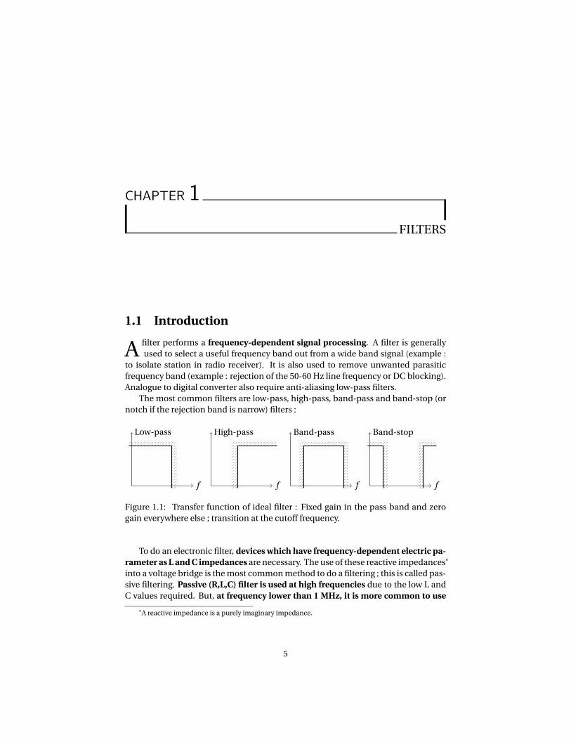
1.1 Introduction
A filter performs a frequency-dependent signal processing. A filter is generallyused to select a useful frequency band out from a wide band signal (example :
to isolate station in radio receiver). It is also used to remove unwanted parasiticfrequency band (example : rejection of the 50-60 Hz line frequency or DC blocking).Analogue to digital converter also require anti-aliasing low-pass filters.
The most common filters are low-pass, high-pass, band-pass and band-stop (ornotch if the rejection band is narrow) filters :
f
Low-pass
f
High-pass
f
Band-pass
f
Band-stop
Figure 1.1: Transfer function of ideal filter : Fixed gain in the pass band and zerogain everywhere else ; transition at the cutoff frequency.
To do an electronic filter, devices which have frequency-dependent electric pa-rameter as L and C impedances are necessary. The use of these reactive impedances*
into a voltage bridge is the most common method to do a filtering ; this is called pas-sive filtering. Passive (R,L,C) filter is used at high frequencies due to the low L andC values required. But, at frequency lower than 1 MHz, it is more common to use
*A reactive impedance is a purely imaginary impedance.
5
1.2. FILTER PARAMETERS CHAPTER 1. FILTERS
active filters made by an operational amplifier in addition to R and C with reason-able values. Furthermore, active filter parameters are less affected* by source andload impedances than passive one.
1.2 Filter parameters
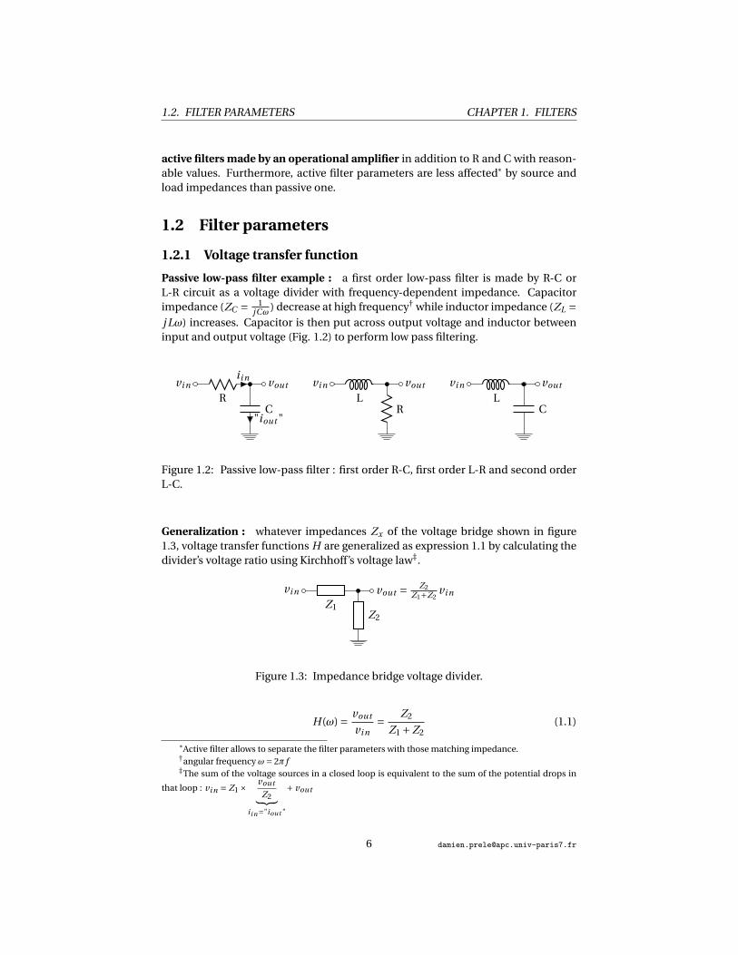
1.2.1 Voltage transfer function
Passive low-pass filter example : a first order low-pass filter is made by R-C orL-R circuit as a voltage divider with frequency-dependent impedance. Capacitorimpedance (ZC = 1
jCω ) decrease at high frequency† while inductor impedance (ZL =j Lω) increases. Capacitor is then put across output voltage and inductor betweeninput and output voltage (Fig. 1.2) to perform low pass filtering.
vi n
R
ii n
C"iout "
vout vi n
LR
vout vi n
LC
vout
Figure 1.2: Passive low-pass filter : first order R-C, first order L-R and second orderL-C.
Generalization : whatever impedances Zx of the voltage bridge shown in figure1.3, voltage transfer functions H are generalized as expression 1.1 by calculating thedivider’s voltage ratio using Kirchhoff’s voltage law‡.
vi n
Z1Z2
vout = Z2Z1+Z2
vi n
Figure 1.3: Impedance bridge voltage divider.
H(ω) = vout
vi n= Z2
Z1 +Z2(1.1)
*Active filter allows to separate the filter parameters with those matching impedance.†angular frequency ω= 2π f‡The sum of the voltage sources in a closed loop is equivalent to the sum of the potential drops in
that loop : vi n = Z1 ×vout
Z2︸ ︷︷ ︸ii n="iout "
+ vout
1.2. FILTER PARAMETERS CHAPTER 1. FILTERS
Voltage transfer functions of filters given in figure 1.2 are then expressed as :
HRC = ZC
R +ZC=
1jCω
R + 1jCω
=⇒ HRC = 1
1+ j RCω(1.2)
HLR = R
R +ZL= R
R + j Lω=⇒ HLR = 1
1+ j LRω
(1.3)
HLC = ZC
ZL +ZC=
1jCω
j Lω+ 1jCω
=⇒ HLC = 1
1−LCω2 (1.4)
+ A filter can also be used to convert a current to a voltage or a voltage to acurrent in addition to a simple filtering *. Considering for example the first R-C lowpass filter in figure 1.2. We can define trans-impedance transfer function vout
ii nand
the trans-admittance transfer function "iout "vi n
:
vout
ii n= vout
"iout "= ZC = 1
jCω−→ Integrator (1.5)
"iout "
vi n= 1
R +ZC= 1
R + 1jCω
= jCω
1+ j RCω−→ High-pass filter (1.6)
1.2.2 S plane (Laplace domain)
Due to the fact that L and C used in filter design has complex impedance, filter trans-fer function H can be represented as a function of a complex number s :
s =σ+ jω (1.7)
Frequency response and stability information can be revealed by plotting in acomplex plane (s plane) roots values of H(s) numerator (zero) and denominator(pole).
• Poles are values of s such that transfer function |H |→∞,
• Zeros are values of s such that transfer function |H | = 0.
Considering the band-pass filter of the figure 1.4, the transfer function HLC R =voutvi n
is given by equation 1.8.
HLC R (s) = R
R +Ls + 1C s
= RC s
1+RC s +LC s2 (1.8)
The order of the filter (Fig. 1.4) is given by the degree of the denominator of theexpression 1.8. A zero corresponds the numerator equal to zero. A pole is given
*To filter a current, two impedances in parallel are require : current divider. In our example without
load impedance ii n = iout . Current transfer function "iout "ii n
is then always equal to 1.

1.2. FILTER PARAMETERS CHAPTER 1. FILTERS
vi n
L C R
vout
Figure 1.4: Passive band-pass LCR filter.
by the denominator equal to zero. Each pole provides a -20dB/decade slope of thetransfer function ; each zero a + 20 dB/decade *. Zero and pole can be real or com-plex. When they are complex, they have a conjugate pair †.Expression 1.8 is characterized by a zero at ω= 0 and two conjugate poles obtainedby nulling it’s denominator (1.9).
0 = 1+RC s +LC s2 −−−−−→di scr i .
∆= (RC )2 −4LC −−−−→r oot s
sp = −RC ±√
(RC )2 −4LC
2LC(1.9)
The two roots allow to obtain poles sp1 and sp2 given on 1.10.
sp = −R
2L± j
√1
LC−
(R
2L
)2
(1.10)
The natural angular frequency ω0 is the module of the pole :
ω0 = |sp1,2 | =1pLC
(1.11)
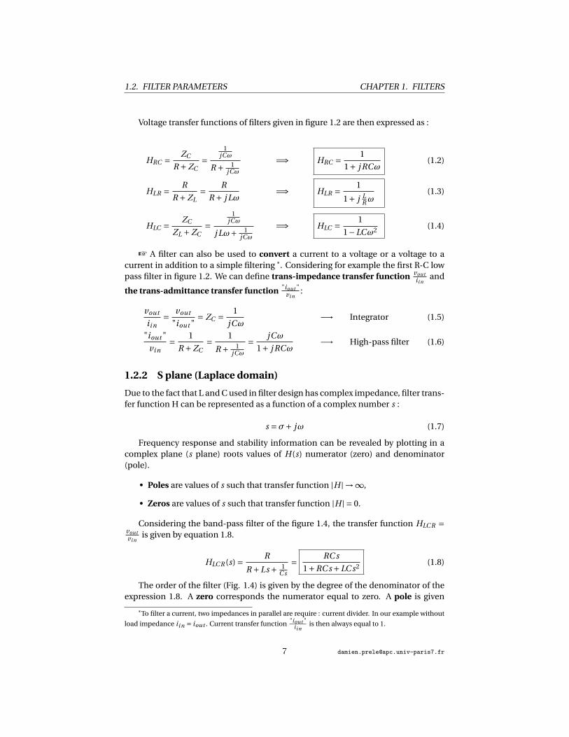
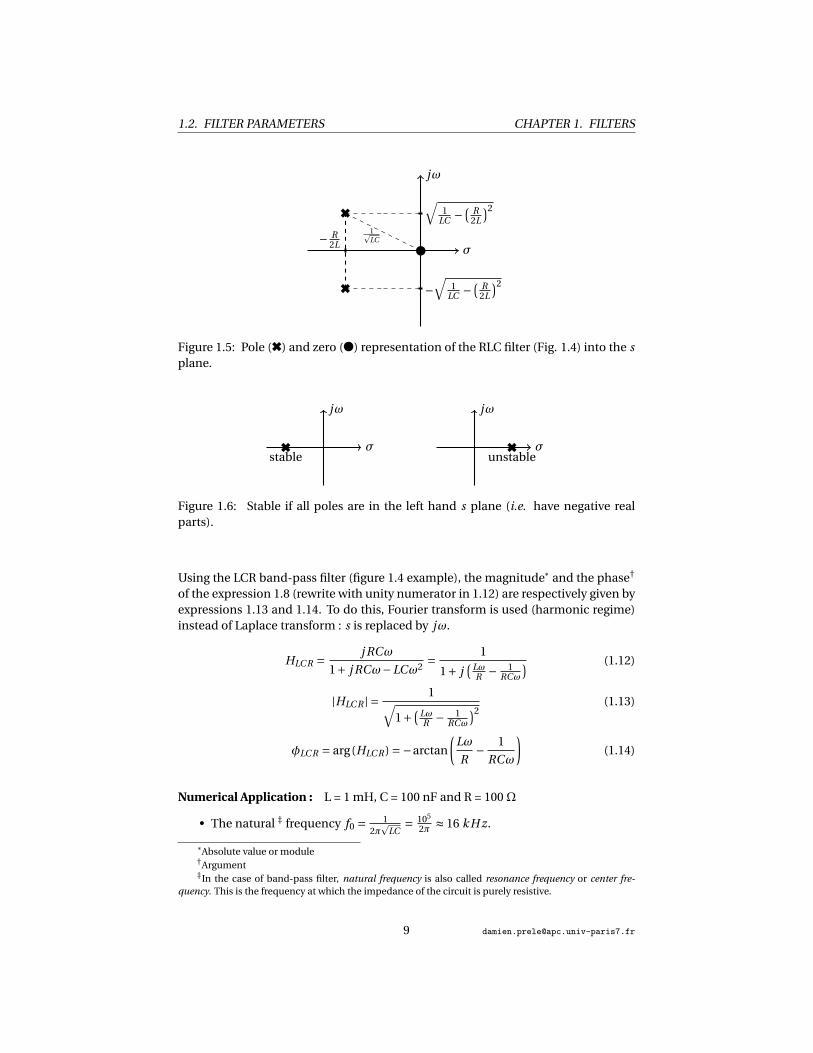
In a s plane, pole and zero allow to locate where the magnitude of the transferfunction is large (near pole), and where it is small (near zero). This provides us un-derstanding of what the filter does at different frequencies and is used to study thestability. Figure 1.5 shows pole (6) and zero (l) in a s plane.
A causal linear system is stable if real part of all poles is negative. On the s plane,this corresponds to a pole localization at the left side (Fig. 1.6).
1.2.3 Bode plot (Fourier domain)
The most common way to represent the transfer function of a filter is the Bode plot.Bode plot is usually a combination of the magnitude |H | and the phase φ of thetransfer function on a log frequency axis.
*H [dB ] = 20log H [l i n.] and a decade correspond to a variation by a factor of ten in frequency. Atimes 10 ordinate increasing on a decade (times 10 abscissa increasing) correspond to a 20dB/decadeslope on a logarithmic scale or also 6dB/octave. A -20dB/decade then correspond to a transfer functiondecreasing by a factor of 10 on a decade
†each conjugate pair has the same real part, but imaginary parts equal in magnitude and opposite insigns
1.2. FILTER PARAMETERS CHAPTER 1. FILTERS
σ
jω
1pLC− R
2Ll
6√
1LC − ( R
2L
)2
6 −√
1LC − ( R
2L
)2
Figure 1.5: Pole (6) and zero (l) representation of the RLC filter (Fig. 1.4) into the splane.
σ
jω
6stable
σ
jω
6unstable
Figure 1.6: Stable if all poles are in the left hand s plane (i.e. have negative realparts).
Using the LCR band-pass filter (figure 1.4 example), the magnitude* and the phase†
of the expression 1.8 (rewrite with unity numerator in 1.12) are respectively given byexpressions 1.13 and 1.14. To do this, Fourier transform is used (harmonic regime)instead of Laplace transform : s is replaced by jω.
HLC R = j RCω
1+ j RCω−LCω2 = 1
1+ j( Lω
R − 1RCω
) (1.12)
|HLC R | = 1√1+ ( Lω
R − 1RCω
)2(1.13)
φLC R = arg(HLC R ) =−arctan
(Lω
R− 1
RCω
)(1.14)
Numerical Application : L = 1 mH, C = 100 nF and R = 100Ω
• The natural ‡ frequency f0 = 12π
pLC
= 105
2π ≈ 16 kH z.
*Absolute value or module†Argument‡In the case of band-pass filter, natural frequency is also called resonance frequency or center fre-
quency. This is the frequency at which the impedance of the circuit is purely resistive.

1.2. FILTER PARAMETERS CHAPTER 1. FILTERS
• The high pass-filter cutoff frequency fc1 = R2πL = f0.
• The low pass-filter cutoff frequency fc2 = 12πRC = f0.
The Bode diagram of this band-pass filter is plotted on figure 1.7.
Figure 1.7: Bode plot of the LCR band-pass filter figure 1.4.
+ Whatever the numerical application, f0 = √fc1 fc2 but f0, fc1 and fc2 are not neces-
sarily equal.
In this numerical application f0 = fc1 = fc2 (Fig 1.7). This correspond to a par-
ticular case where the quality factor Q = 1R
√LC = 1
100
√10−310−7 = 1. For other numerical
application (i.e. Q 6= 1), f0 is different than fc1 and fc2 (Fig 1.8).
Quality factor Q
Quality factor Q is a dimensionless parameter which indicates how much is thesharpness of a multi-pole filter response around its cut-off (or center *) frequency. Inthe case of a band-pass filter, its expression 1.15 is the ratio of the center frequencyto the -3 dB bandwidth (BW) and is given for series and parallel LCR circuit.
Q = f0
BW
∣∣∣band-pass filter
= 1
R
√L
C
∣∣∣series LCR
= R
√C
L
∣∣∣parallel LCR
(1.15)
*for a band-pass filter
1.2. FILTER PARAMETERS CHAPTER 1. FILTERS
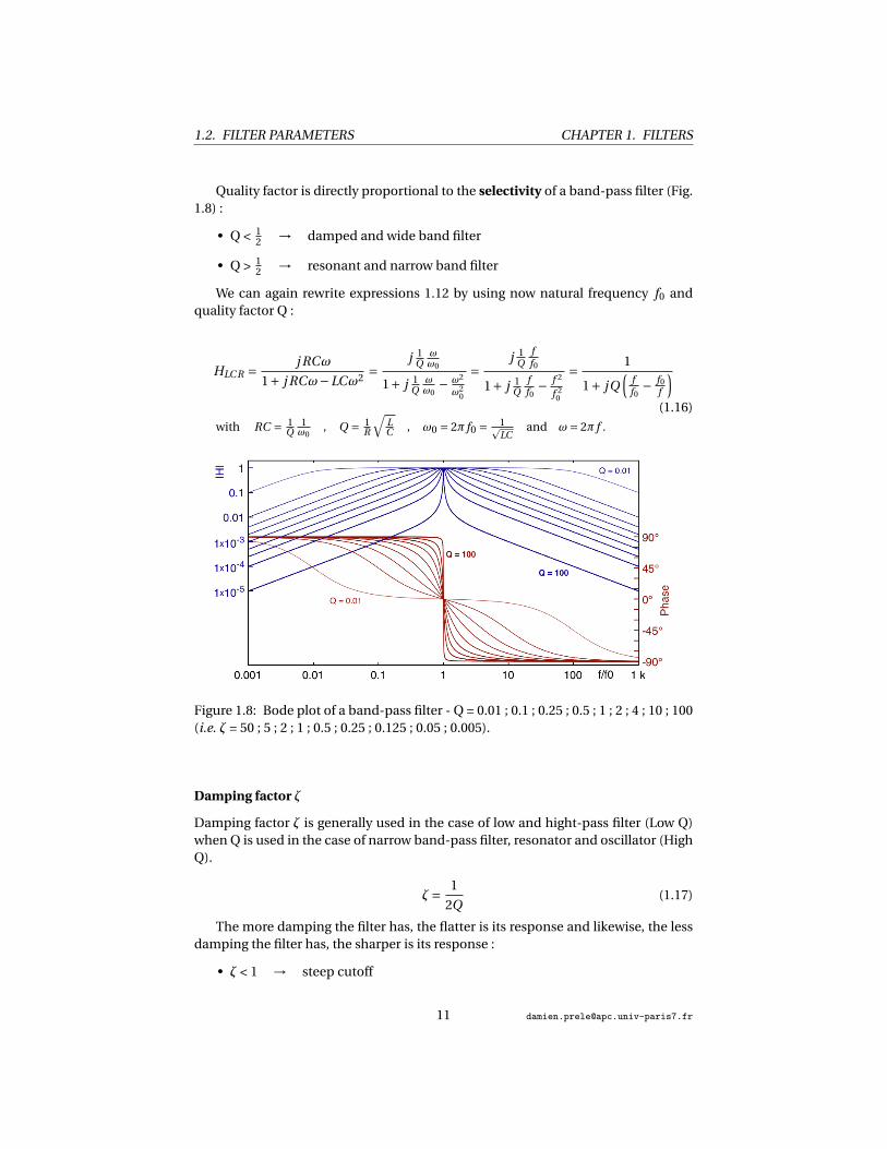
Quality factor is directly proportional to the selectivity of a band-pass filter (Fig.1.8) :
• Q < 12 → damped and wide band filter
• Q > 12 → resonant and narrow band filter
We can again rewrite expressions 1.12 by using now natural frequency f0 andquality factor Q :
HLC R = j RCω
1+ j RCω−LCω2 =j 1
Qωω0
1+ j 1Q
ωω0
− ω2
ω20
=j 1
Qff0
1+ j 1Q
ff0− f 2
f 20
= 1
1+ jQ(
ff0− f0
f
)(1.16)
with RC = 1Q
1ω0
, Q = 1R
√LC , ω0 = 2π f0 = 1p
LCand ω= 2π f .
Figure 1.8: Bode plot of a band-pass filter - Q = 0.01 ; 0.1 ; 0.25 ; 0.5 ; 1 ; 2 ; 4 ; 10 ; 100(i.e. ζ = 50 ; 5 ; 2 ; 1 ; 0.5 ; 0.25 ; 0.125 ; 0.05 ; 0.005).
Damping factor ζ
Damping factor ζ is generally used in the case of low and hight-pass filter (Low Q)when Q is used in the case of narrow band-pass filter, resonator and oscillator (HighQ).
ζ= 1
2Q(1.17)
The more damping the filter has, the flatter is its response and likewise, the lessdamping the filter has, the sharper is its response :
• ζ < 1 → steep cutoff
1.3. CASCADING FILTER STAGES CHAPTER 1. FILTERS
• ζ = 1 → critical damping
• ζ > 1 → slow cutoff
Expression 1.12 may be rewritten using damping factor :
HLC R = j RCω
1+ j RCω−LCω2 =j 2ζ ω
ω0
1+ j 2ζ ωω0
− ω2
ω20
(1.18)
1.3 Cascading filter stages
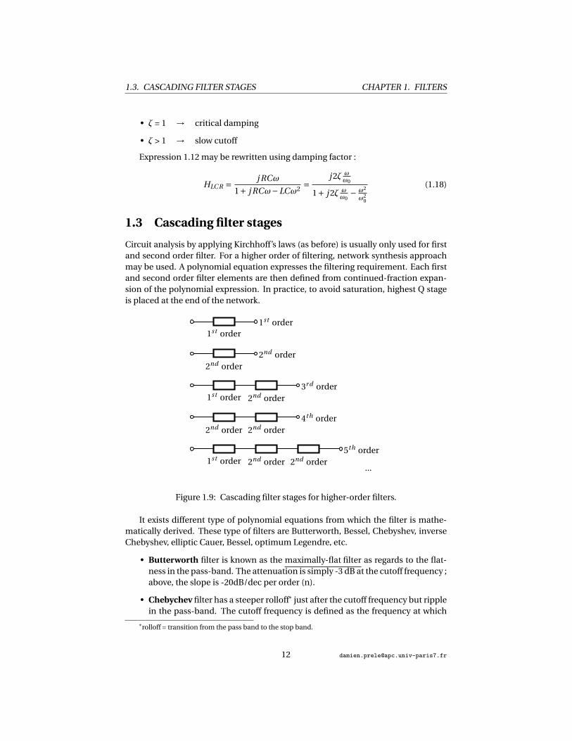
Circuit analysis by applying Kirchhoff’s laws (as before) is usually only used for firstand second order filter. For a higher order of filtering, network synthesis approachmay be used. A polynomial equation expresses the filtering requirement. Each firstand second order filter elements are then defined from continued-fraction expan-sion of the polynomial expression. In practice, to avoid saturation, highest Q stageis placed at the end of the network.
1st order1st order
2nd order2nd order
1st order 2nd order3r d order
2nd order 2nd order4th order
1st order 2nd order 2nd order5th order
...
Figure 1.9: Cascading filter stages for higher-order filters.
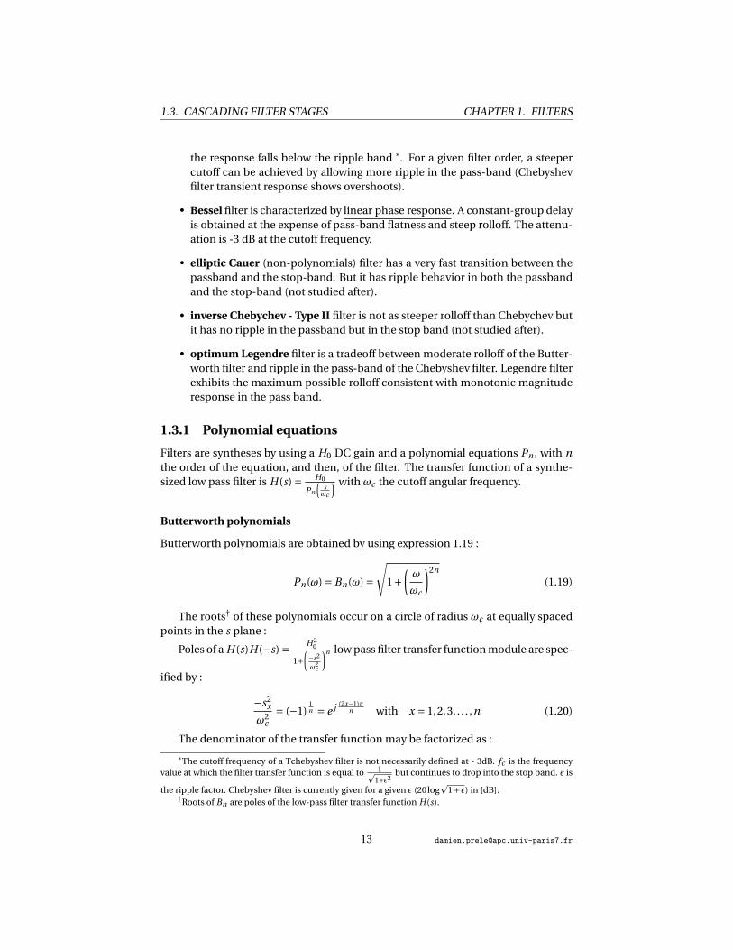
It exists different type of polynomial equations from which the filter is mathe-matically derived. These type of filters are Butterworth, Bessel, Chebyshev, inverseChebyshev, elliptic Cauer, Bessel, optimum Legendre, etc.
• Butterworth filter is known as the maximally-flat filter as regards to the flat-ness in the pass-band. The attenuation is simply -3 dB at the cutoff frequency ;above, the slope is -20dB/dec per order (n).
• Chebychev filter has a steeper rolloff* just after the cutoff frequency but ripplein the pass-band. The cutoff frequency is defined as the frequency at which
*rolloff = transition from the pass band to the stop band.
1.3. CASCADING FILTER STAGES CHAPTER 1. FILTERS
the response falls below the ripple band *. For a given filter order, a steepercutoff can be achieved by allowing more ripple in the pass-band (Chebyshevfilter transient response shows overshoots).
• Bessel filter is characterized by linear phase response. A constant-group delayis obtained at the expense of pass-band flatness and steep rolloff. The attenu-ation is -3 dB at the cutoff frequency.
• elliptic Cauer (non-polynomials) filter has a very fast transition between thepassband and the stop-band. But it has ripple behavior in both the passbandand the stop-band (not studied after).
• inverse Chebychev - Type II filter is not as steeper rolloff than Chebychev butit has no ripple in the passband but in the stop band (not studied after).
• optimum Legendre filter is a tradeoff between moderate rolloff of the Butter-worth filter and ripple in the pass-band of the Chebyshev filter. Legendre filterexhibits the maximum possible rolloff consistent with monotonic magnituderesponse in the pass band.
1.3.1 Polynomial equations
Filters are syntheses by using a H0 DC gain and a polynomial equations Pn , with nthe order of the equation, and then, of the filter. The transfer function of a synthe-sized low pass filter is H(s) = H0
Pn
(sωc
) with ωc the cutoff angular frequency.
Butterworth polynomials
Butterworth polynomials are obtained by using expression 1.19 :
Pn(ω) = Bn(ω) =√
1+(ω
ωc
)2n
(1.19)
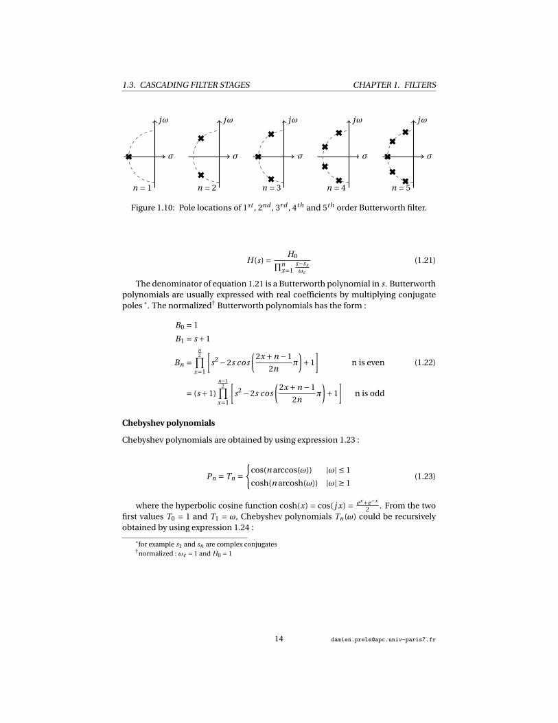
The roots† of these polynomials occur on a circle of radius ωc at equally spacedpoints in the s plane :
Poles of a H(s)H(−s) = H 20
1+(−s2
ω2c
)n low pass filter transfer function module are spec-
ified by :
−s2x
ω2c
= (−1)1n = e j (2x−1)π
n with x = 1,2,3, . . . ,n (1.20)
The denominator of the transfer function may be factorized as :
*The cutoff frequency of a Tchebyshev filter is not necessarily defined at - 3dB. fc is the frequencyvalue at which the filter transfer function is equal to 1p
1+ε2but continues to drop into the stop band. ε is
the ripple factor. Chebyshev filter is currently given for a given ε (20logp
1+ε) in [dB].†Roots of Bn are poles of the low-pass filter transfer function H(s).
1.3. CASCADING FILTER STAGES CHAPTER 1. FILTERS
σ
n = 1
jω
6 σ
n = 2
jω
6
6
σ
n = 3
jω
6
6
6
σ
n = 4
jω
6
6
6
6
σ
n = 5
jω
66
6
66
Figure 1.10: Pole locations of 1st , 2nd , 3r d , 4th and 5th order Butterworth filter.
H(s) = H0∏nx=1
s−sxωc
(1.21)
The denominator of equation 1.21 is a Butterworth polynomial in s. Butterworthpolynomials are usually expressed with real coefficients by multiplying conjugatepoles *. The normalized† Butterworth polynomials has the form :
B0 = 1
B1 = s +1
Bn =n2∏
x=1
[s2 −2s cos
(2x +n −1
2nπ
)+1
]n is even
= (s +1)
n−12∏
x=1
[s2 −2s cos
(2x +n −1
2nπ
)+1
]n is odd
(1.22)
Chebyshev polynomials
Chebyshev polynomials are obtained by using expression 1.23 :
Pn = Tn =
cos(n arccos(ω)) |ω| ≤ 1
cosh(n arcosh(ω)) |ω| ≥ 1(1.23)
where the hyperbolic cosine function cosh(x) = cos( j x) = ex+e−x
2 . From the twofirst values T0 = 1 and T1 = ω, Chebyshev polynomials Tn(ω) could be recursivelyobtained by using expression 1.24 :
*for example s1 and sn are complex conjugates†normalized : ωc = 1 and H0 = 1
1.3. CASCADING FILTER STAGES CHAPTER 1. FILTERS
T0 = 1
T1 =ω
Tn = 2ωTn−1 −Tn−2
T2 = 2ω2 −1
T3 = 4ω3 −3ω
T4 = 8ω4 −8ω2 +1
. . .
(1.24)
Chebyshev low-pass filter frequency response is generally obtained by using aslightly more complex expression than for a Butterworth one :
|H(s)| = H ′0√
1+ε2T 2n
(ωωc
) (1.25)
where ε is the ripple factor *. Even if H ′0 = 1, magnitude of a Chebyshev low-
pass filter is not necessarily equal to 1 at low frequency (ω = 0). Gain will alternatebetween maxima at 1 and minima at 1p
1+ε2.
Tn
(ω
ωc= 0
)=
±1 n is even
0 n is odd⇒ H
(ω
ωc= 0
)=
1p
1+ε2n is even
1 n is odd(1.26)
At the cutoff angular frequency ωc , the gain is also equal to 1p1+ε2
(but ∀n) and,
as the frequency increases, it drops into the stop band.
Tn
(ω
ωc= 1
)=±1 ∀n ⇒ H
(ω
ωc= 1
)=± 1p
1+ε2∀n (1.27)
Finally, conjugate poles sx (equation 1.28 †) of expression 1.25 are obtained bysolving equation 0 = 1+ε2T 2
n :
sx = sin
(2x −1
n
1
2π
)sinh
(1
narcsinh
1
ε
)+ j cos
(2x −1
n
1
2π
)cosh
(1
narcsinh
1
ε
)(1.28)
Using poles, transfer function of a Chebyshev low-pass filter is rewritten as equa-tion 1.25 :
H(s) =
1p
1+ε2∏nx=1
s−sxωc
n is even
1∏nx=1
s−sxωc
n is odd(1.29)
*ε= 1 for the other polynomials filter and is then not represented†Poles are located on a centered ellipse in s plane ; with real axis of length sinh
(1n arcsinh 1
ε
)and
imaginary axis of length cosh(
1n arcsinh 1
ε
).
1.3. CASCADING FILTER STAGES CHAPTER 1. FILTERS
Bessel polynomials
Bessel polynomials are obtained by using expression 1.30 :
Pn = θn =n∑
x=0sx (2n −x)!
2n−x x!(n −x)!
θ1 = s +1
θ2 = s2 +3s +3
θ3 = s3 +6s2 +15s +15
. . .
(1.30)
Bessel low-pass filter frequency response is given by expression 1.31 and is alsogiven for n = 2 (delay normalized second-order Bessel low-pass filter).
θn(0)
θn
(sωc
) =⇒n = 2
3(sωc
)2 +3 sωc
+3= 1
13
(sωc
)2 + sωc
+1(1.31)
However, Bessel polynomials θn have been normalized to unit delay at ωωc
= 0(delay normalized) and are not directly usable for classical cutoff frequency at -3 dBstandard (frequency normalized).
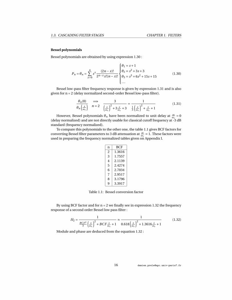
To compare this polynomials to the other one, the table 1.1 gives BCF factors forconverting Bessel filter parameters to 3 dB attenuation at ω
ωc= 1. These factors were
used in preparing the frequency normalized tables given on Appendix I.
n BCF2 1.36163 1.75574 2.11395 2.42746 2.70347 2.95178 3.17969 3.3917
Table 1.1: Bessel conversion factor
By using BCF factor and for n = 2 we finally see in expression 1.32 the frequencyresponse of a second order Bessel low pass filter :
H2 = 1
BC F 2
3
(sωc
)2 +BC F sωc
+1≈ 1
0.618(
sωc
)2 +1.3616 sωc
+1(1.32)
Module and phase are deduced from the equation 1.32 :
1.3. CASCADING FILTER STAGES CHAPTER 1. FILTERS
|H2| = 1√(1−0.618ω
2
ω2c
)2 +(1.3616 ω
ωc
)2
φ= arg(H2) =−arctan
1.3616 ωωc
1−0.618ω2
ω2c
(1.33)
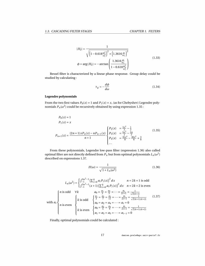
Bessel filter is characterized by a linear phase response. Group delay could bestudied by calculating :
τg =−dφ
dω(1.34)
Legendre polynomials
From the two first values P0(x) = 1 and P1(x) = x, (as for Chebyshev) Legendre poly-nomials Pn(ω2) could be recursively obtained by using expression 1.35 :
P0(x) = 1
P1(x) = x
Pn+1(x) = (2n +1)xPn(x)−nPn−1(x)
n +1
P2(x) = 3x2
2 − 12
P3(x) = 5x3
2 − 3x2
P4(x) = 35x4
8 − 30x2
8 + 38
. . .
(1.35)
From these polynomials, Legendre low-pass filter (expression 1.36) also calledoptimal filter are not directly defined from Pn but from optimal polynomials Ln(ω2)described on expressions 1.37.
H(ω) = 1√1+Ln(ω2)
(1.36)
Ln(ω2) =∫ 2ω2−1
−1
(∑ki=0 ai Pi (x)
)2d x n = 2k +1 is odd∫ 2ω2−1
−1 (x +1)(∑k
i=0 ai Pi (x))2
d x n = 2k +2 is even
with ai
n is odd ∀k a0 = a13 = a2
5 = ·· · = ai2i+1 = 1p
2(k+1)
n is even
k is odd
a13 = a3
7 = a511 = ·· · = ai
2i+1 = 1p2(k+1)(k+2)
a0 = a2 = a4 = ·· · = ai = 0
k is even
a0 = a2
5 = a49 = ·· · = ai
2i+1 = 1p2(k+1)(k+2)
a1 = a3 = a5 = ·· · = ai−1 = 0
(1.37)
Finally, optimal polynomials could be calculated :
1.3. CASCADING FILTER STAGES CHAPTER 1. FILTERS
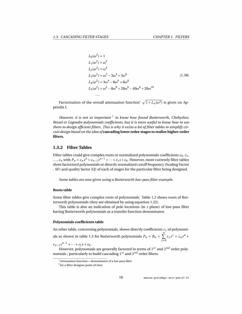
L0(ω2) = 1
L1(ω2) =ω2
L2(ω2) =ω4
L3(ω2) =ω2 −3ω4 +3ω6
L4(ω2) = 3ω4 −8ω6 +6ω8
L5(ω2) =ω2 −8ω8 +28ω6 −40ω8 +20ω10
. . .
(1.38)
Factorization of the overall attenuation function*√
1+Ln(ω2) is given on Ap-pendix I.
However, it is not so important † to know how found Butterworth, Chebyshev,Bessel or Legendre polynomials coefficients; but it is more useful to know how to usethem to design efficient filters. This is why it exists a lot of filter tables to simplify cir-cuit design based on the idea of cascading lower order stages to realize higher-orderfilters.
1.3.2 Filter Tables
Filter tables could give complex roots or normalized polynomials coefficients c0, c1,. . . , cn with Pn = cn sn +cn−1sn−1+·· ·+c1s+c0. However, more currently filter tablesshow factorized polynomials or directly normalized cutoff frequency (Scaling Factor- SF) and quality factor (Q) of each of stages for the particular filter being designed.
Some tables are now given using a Butterworth low-pass filter example.
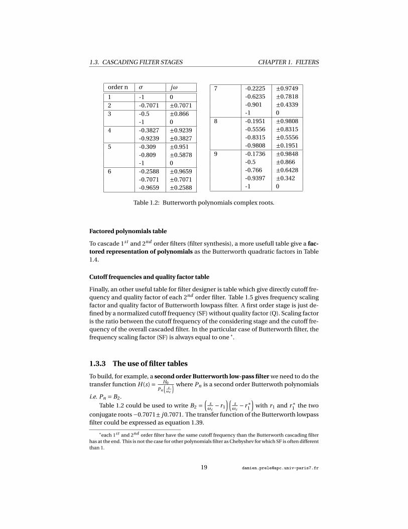
Roots table
Some filter tables give complex roots of polynomials. Table 1.2 shows roots of But-terworth polynomials (they are obtained by using equation 1.22).
This table is also an indication of pole locations (in s plane) of low-pass filterhaving Butterworth polynomials as a transfer function denominator.
Polynomials coefficients table
An other table, concerning polynomials, shows directly coefficients cx of polynomi-
als as shown in table 1.3 for Butterworth polynomials Pn = Bn =n∑
x=0cx sx = cn sn +
cn−1sn−1 +·· ·+c1s + c0.However, polynomials are generally factored in terms of 1st and 2nd order poly-
nomials ; particularly to build cascading 1st and 2nd order filters.
*Attenuation function = denominator of a low pass filter†for a filter designer point of view
1.3. CASCADING FILTER STAGES CHAPTER 1. FILTERS
order n σ jω
1 -1 02 -0.7071 ±0.70713 -0.5 ±0.866
-1 04 -0.3827 ±0.9239
-0.9239 ±0.38275 -0.309 ±0.951
-0.809 ±0.5878-1 0
6 -0.2588 ±0.9659-0.7071 ±0.7071-0.9659 ±0.2588
7 -0.2225 ±0.9749-0.6235 ±0.7818-0.901 ±0.4339-1 0
8 -0.1951 ±0.9808-0.5556 ±0.8315-0.8315 ±0.5556-0.9808 ±0.1951
9 -0.1736 ±0.9848-0.5 ±0.866-0.766 ±0.6428-0.9397 ±0.342-1 0
Table 1.2: Butterworth polynomials complex roots.
Factored polynomials table
To cascade 1st and 2nd order filters (filter synthesis), a more usefull table give a fac-tored representation of polynomials as the Butterworth quadratic factors in Table1.4.
Cutoff frequencies and quality factor table
Finally, an other useful table for filter designer is table which give directly cutoff fre-quency and quality factor of each 2nd order filter. Table 1.5 gives frequency scalingfactor and quality factor of Butterworth lowpass filter. A first order stage is just de-fined by a normalized cutoff frequency (SF) without quality factor (Q). Scaling factoris the ratio between the cutoff frequency of the considering stage and the cutoff fre-quency of the overall cascaded filter. In the particular case of Butterworth filter, thefrequency scaling factor (SF) is always equal to one *.
1.3.3 The use of filter tables
To build, for example, a second order Butterworth low-pass filter we need to do thetransfer function H(s) = H0
Pn
(sωc
) where Pn is a second order Butterwoth polynomials
i.e. Pn = B2.
Table 1.2 could be used to write B2 =(
sωc
− r1
)(sωc
− r∗1
)with r1 and r∗
1 the two
conjugate roots −0.7071± j 0.7071. The transfer function of the Butterworth lowpassfilter could be expressed as equation 1.39.
*each 1st and 2nd order filter have the same cutoff frequency than the Butterworth cascading filterhas at the end. This is not the case for other polynomials filter as Chebyshev for which SF is often differentthan 1.

1.3. CASCADING FILTER STAGES CHAPTER 1. FILTERS
n c0 c1 c2 c3 c4 c5 c6 c7 c8 c9 c10
1 1 12 1 1.41 13 1 2 2 14 1 2.61 3.41 2.61 15 1 3.24 5.24 5.24 3.24 16 1 3.86 7.46 9.14 7.46 3.86 17 1 4.49 10.1 14.59 14.59 10.1 4.49 18 1 5.13 13.14 21.85 25.69 21.85 13.14 5.13 19 1 5.76 16.58 31.16 41.99 41.99 31.16 16.58 5.76 1
10 1 6.39 20.43 42.8 64.88 74.23 64.88 42.8 20.43 6.39 1
Table 1.3: Butterworth polynomials coefficients cx . Pn = Bn =n∑
x=0cx sx = cn sn +
cn−1sn−1 +·· ·+c1s + c0.
n Pn = Bn
1 s +12 s2 +1.4142s +13 (s +1)(s2 + s +1)4 (s2 +0.7654s +1)(s2 +1.8478s +1)5 (s +1)(s2 +0.618s +1)(s2 +1.618s +1)6 (s2 +0.5176s +1)(s2 +1.4142s +1)(s2 +1.9319s +1)7 (s +1)(s2 +0.445s +1)(s2 +1.247s +1)(s2 +1.8019s +1)8 (s2 +0.3902s +1)(s2 +1.1111s +1)(s2 +1.6629s +1)(s2 +1.9616s +1)9 (s +1)(s2 +0.3473s +1)(s2 + s +1)(s2 +1.5321s +1)(s2 +1.8794s +1)
10 (s2 +0.3129s +1)(s2 +0.908s +1)(s2 +1.4142s +1)(s2 +1.782s +1)(s2 +1.9754s +1)
Table 1.4: Butterworth polynomials quadratic factors.
H(s) = H0
B2
(sωc
) = H0(sωc
+0.7071− j 0.7071)(
sωc
+0.7071+ j 0.7071) (1.39)
The denominator development of the expression 1.39 give a quadratic form (ex-pression 1.40) which clearly shows Butterworth polynomial coefficients given on ta-ble 1.3 and quadratic factors of table 1.4. It is also clear that expression 1.40 is similarto a classical representation of a transfer function with quality factor where SF andQ are finally what we can directly obtain from the table 1.5.

1.3. CASCADING FILTER STAGES CHAPTER 1. FILTERS
order n 1st st ag e 2nd st ag e 3r d st ag e 4th st ag e 5th st ag eSF Q SF Q SF Q SF Q SF Q
1 12 1 0.70713 1 1 14 1 0.5412 1 1.30655 1 0.618 1 1.6181 16 1 0.5177 1 0.7071 1 1.93207 1 0.5549 1 0.8019 1 2.2472 18 1 0.5098 1 0.6013 1 0.8999 1 2.56289 1 0.5321 1 0.6527 1 1 1 2.8802 1
10 1 0.5062 1 0.5612 1 0.7071 1 1.1013 1 3.1969
Table 1.5: Butterworth normalized cutoff frequency (Scaling Factor - SF) and qualityfactor (Q) for each stages.
H(s) = H0(sωc
)2 +1.41 sωc
+1= H0
1+ j 1Q
fSF fc
− f 2
SF 2 f 2c
with
SF = 1
Q = 11.41 = 0.7071
(1.40)Bode diagram of this low pass filter could be expressed as equation 1.41 and plot-
ted as figure 1.11.
|H(ω)| = 1√[1−
(ωωc
)2]2
+(1.41 ω
ωc
)2with H0 = 1
φ(ω) = arg(H) =−arctan1.41 ω
ωc
1−(ωωc
)2
(1.41)
1.3.4 Conversion from low-pass filter
Low-pass to high-pass filter Filter tables give polynomials for low and high-passfilter. To obtain a high pass filter, a first order low pass filter transfer function H0
c0+c1s
becomes H∞sc1+c0s ; and a second order low pass filter transfer function H0
c0+c1s+c2s2 be-
comes H∞s2
c2+c1s+c0s2 . Figure 1.12 shows low and high pass filter with H0 and H∞ *.
*in practice, there is always a frequency limitation which constitute a low pass filter, so that an idealhigh pass filter never exists and H∞ → 0. So, in the case of real high pass filter, H∞ signifies more the gainjust after the cut-off frequency than that at infinity.

1.3. CASCADING FILTER STAGES CHAPTER 1. FILTERS
Figure 1.11: Bode plot of a second order Butterworth low pass filter.
HLP1 =H0
c0 + c1s⇒ HHP1 =
H∞c0 + c1/s
HLP2 =H0
c0 + c1s + c2s2 ⇒ HHP2 =H∞
c0 + c1/s + c2/s2
(1.42)
Low to High pass filter conversion: s ⇒ s−1
Figure 1.12: H0 the low frequency gain of a low-pass filter and H∞ the high fre-quency gain of a high-pass filter.
Band-pass filter For band-pass filter, it exists specific tables which give specificcoefficients given for different bandwidth (BW). However, a low pass filter transfer
1.4. FILTER SYNTHESYS CHAPTER 1. FILTERS
function could be converted in band-pass filter by replacing s by f0BW
(s + s−1
); where
f0BW is equal to the quality factor Q.
Low to Band-pass filter conversion: s ⇒Q(s + s−1)
Band-reject filter A low pass filter transfer function is converted in band-reject fil-ter by replacing s by 1
f0BW (s+s−1)
.
Low to Band-reject filter conversion: s ⇒Q−1 (s + s−1)−1
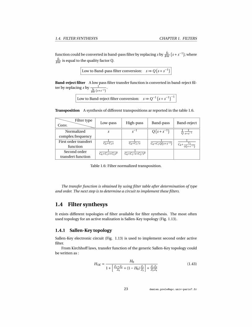
Transposition A synthesis of different transpositions ar reported in the table 1.6.
XXXXXXXXXXConv.Filter type
Low-pass High-pass Band-pass Band-reject
Normalizedcomplex frequency
s s−1 Q(s + s−1
) 1Q
1s+s−1
First order transfertfunction
1C0+C1s
1C0+C1/s
1C0+C1Q(s+s−1)
1
C0+ C1Q(s+s−1)
Second ordertransfert function
1C0+C1s+C2s2
1C0+C1/s+C2/s2
Table 1.6: Filter normalized transposition.
The transfer function is obtained by using filter table after determination of typeand order. The next step is to determine a circuit to implement these filters.
1.4 Filter synthesys
It exists different topologies of filter available for filter synthesis. The most oftenused topology for an active realization is Sallen-Key topology (Fig. 1.13).
1.4.1 Sallen-Key topology
Sallen-Key electronic circuit (Fig. 1.13) is used to implement second order activefilter.
From Kirchhoff laws, transfer function of the generic Sallen-Key topology couldbe written as :
HSK = H0
1+[
Z1+Z2Z4
+ (1−H0) Z1Z3
]+ Z1 Z2
Z3 Z4
(1.43)

1.4. FILTER SYNTHESYS CHAPTER 1. FILTERS
vi n
Z1 Z2Z4
H0
Z3
vout
Figure 1.13: Sallen-Key generic topology.
Sallen-Key low-pass filter
A low-pass filter is easily obtained from this circuit. Figure 1.14 show a Sallen-Keylow-pass filter.
vi n
R1 R2C2
H0
C1
vout
Figure 1.14: Sallen-Key low-pass filter.
The transfer function of this Sallen-Key low-pass filter is given by equation 1.44.
HSKLP = H0
1+ [(R1 +R2)C2 +R1C1(1−H0)
]s +R1R2C1C2s2
= H0
c0 + c1s + c2s2
= H0
1+ j 1Q
fSF fc
− f 2
SF 2 f 2c
with
SF fc = 1
2πp
R1R2C1C2
Q =p
R1R2C1C2(R1+R2)C2+R1C1(1−H0)
(1.44)
This second order Sallen-Key filter can be used to realize one complex-pole pairin the transfer function of a low-pass cascading filter. Values of the Sallen-Key cir-cuit could be chosen to correspond to a polynomials coefficients (as Butterworth,Chebyshev or Bessel).

1.4. FILTER SYNTHESYS CHAPTER 1. FILTERS
Sallen-Key high-pass filter
To transform a low-pass filter to a high-pass filter, all resistors are replaced by capac-itor and capacitors by resistors :
vi n
C1 C2 R2
H0
R1
vout
Figure 1.15: Sallen-Key high-pass filter.
The transfer function of this Sallen-Key high-pass filter is given by equation 1.45.
HSKHP = H0R1R2C1C2s2
1+ [R1(C1 +C2)+R2C2(1−H0)
]s +R1R2C1C2s2
= H0
c0 + c1s + c2
s2
=H0
c2c0
s2
c0 + c1c2c0
s + c2s2
=H0
− f 2
SF 2 f 2c
1+ j 1Q
fSF fc
− f 2
SF 2 f 2c
with
SF fc = 1
2πp
R1R2C1C2
Q =p
R1R2C1C2R1(C1+C2)+R2C2(1−H0)
(1.45)
Sallen-Key band-pass filter
Band-pass filter could be obtained by placing in series a high and a low pass filter asillustrated in figure 1.16. Cut-off frequency of the low pass filter need to be higherthan the high-pass one ; unless you want to make a resonant filter.
Low-pass High-passBand-pass filter
Figure 1.16: Cascading low and high pass filter for band-pass filtering.
A possible arrangement of generic Sallen-Key topology in band-pass configura-tion is given in figure 1.17.
But we can also found more complicated band-pass filter as figure 1.18 basedon voltage-controlled voltage-source (VCVS) filter topology which gives the transferfunction expressed in equation 1.46.

1.4. FILTER SYNTHESYS CHAPTER 1. FILTERS
vi n
R1 C2 R2
H0
C1
vout
Figure 1.17: Sallen-Key band-pass filter.
vi n
R1
C2 R2C1
H0
R3
vout
Figure 1.18: Voltage-controlled voltage-source (VCVS) filter topology band-pass fil-ter.
HV CV SBP = H0
R2R3C2R1+R3
s
1+ R1R3(C1+C2)+R2R3C2+R1R2C2(1−H0)R1+R3
s + R1R2R3C1C2R1+R3
s2
= H ′0s
c0 + c1s + c2s2 with H ′0 = H0
R2R3C2
R1 +R3
= H ′0s
1+ j 1Q
fSF fc
− f 2
SF 2 f 2c
with
SF fc = 1
2π
√R1+R3
R1R2R3C1C2
Q =p
(R1+R3)R1R2R3C1C2R1R3(C1+C2)+R2R3C2−R1R2C2(1−H0)
(1.46)
Sallen-Key band-reject filter
Unlike the band-pass filter, a notch filter can not be obtained by a series connectionof low and high pass filters. But a summation of the output * of a low and a high passfilter could be a band-reject filter if cut-off frequency of the low pass filter is lowerthan the high-pass one. This correspond to paralleling high and low pass filter.
Band-reject filter could be obtained by placing in parallel a high and a low passfilter as illustrated in figure 1.19.
*In practice it is not possible to connect two outputs each other without taking some precautions.

1.4. FILTER SYNTHESYS CHAPTER 1. FILTERS
High-pass
Band-reject filter
Low-pass
Figure 1.19: Paralleling low and high pass filter for band-pass filtering.
A band-reject filter is finally obtained by using circuit of figure 1.20.
vi n
R R
C C
R/2
H0
2C
vout
Figure 1.20: Sallen-Key band-reject filter.
Parameters of this simplified Sallen-Key band reject filter is given by expression1.47.
SF fc = 1
2πp
RC
Q = 1
4−2H0
(1.47)
1.5. AMPLITUDE RESPONSES CHAPTER 1. FILTERS
1.5 Amplitude responses
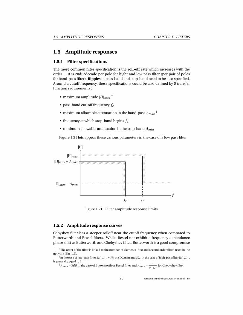
1.5.1 Filter specifications
The more common filter specification is the roll-off rate which increases with theorder *. It is 20dB/decade per pole for hight and low pass filter (per pair of polesfor band-pass filter). Ripples in pass-band and stop-band need to be also specified.Around a cutoff frequency, these specifications could be also defined by 5 transferfunction requirements :
• maximum amplitude |H |max†
• pass-band cut-off frequency fc
• maximum allowable attenuation in the band-pass Amax‡
• frequency at which stop-band begins fs
• minimum allowable attenuation in the stop-band Ami n
Figure 1.21 lets appear these various parameters in the case of a low pass filter :
f
|H|
|H|max
|H|max − Amax
fp fs
|H|max − Ami n
Figure 1.21: Filter amplitude response limits.
1.5.2 Amplitude response curves
Cebyshev filter has a steeper rolloff near the cutoff frequency when compared toButterworth and Bessel filters. While, Bessel not exhibit a frequency dependancephase shift as Butterworth and Chebyshev filter. Butterworth is a good compromise
*The order of the filter is linked to the number of elements (first and second order filter) used in thenetwork (Fig. 1.9).
†in the case of low-pass filter, |H |max = H0 the DC gain and H∞ in the case of high-pass filter |H |max ,is generally equal to 1.
‡ Amax = 3dB in the case of Butterworth or Bessel filter and Amax = 1p1+ε2
for Chebyshev filter.

1.5. AMPLITUDE RESPONSES CHAPTER 1. FILTERS
as regards to the rolloff, while having a maximaly-flat frequency response. Finally,Legendre filter has the steeper rollof without ripple in the band pass. These kind ofcomparison between Butterworth, Chebyshev, Bessel and Legendre filter is outlinedby figure 1.22 and tables 1.7 and 1.8.
Rolloff steepness
BESSEL - BUTTERWORTH - CHEBYSHEV
phase non-linearity
Figure 1.22: Steepness and phase linearity filter comparison.
XXXXXXXXXXFilterProperties
Advantages Disadvantages
Butterworth Maximally flat magnituderesponse in the pass-band
Overshoot and ringing instep response
Chebyshev Better attenuation beyondthe pass-band
Ripple in pass-band. Evenmore ringing in step
responseBessel Excellent step response Even poorer attenuation
beyond the pass-bandLegendre Better rolloff without
ripple in pass-bandpass-band not so flat
Table 1.7: Butterworth, Chebyshev, Bessel and Legendre filter advan-tages/disadvantages.
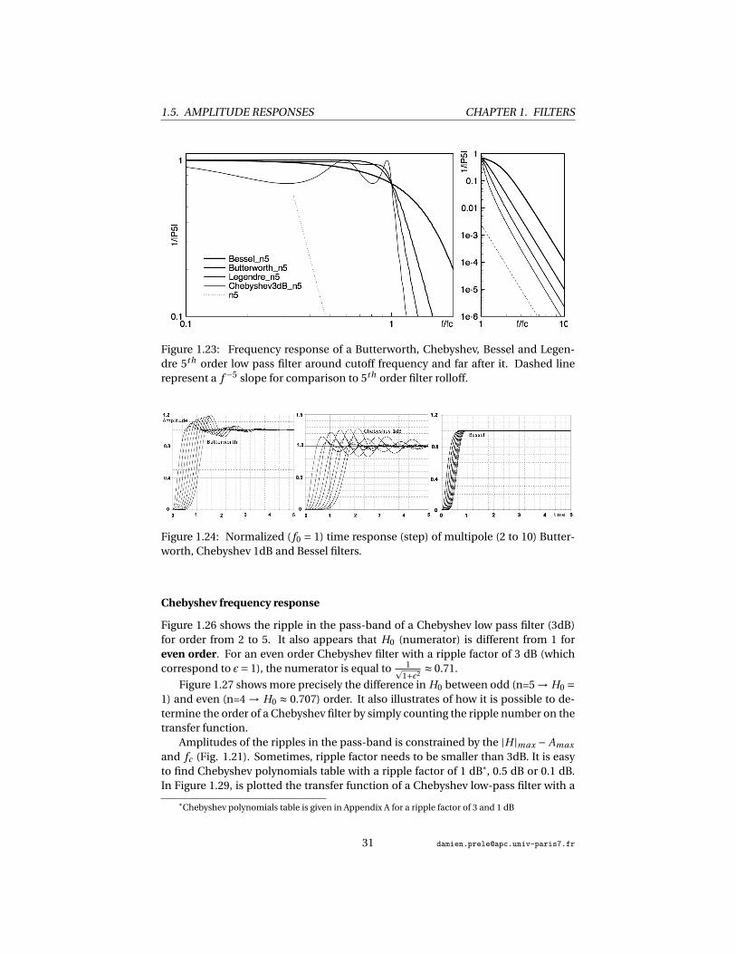
The response of Butterworth, Chebyshev, Bessel and Legendre low pass filter iscompared. To do this, polynomial tables given in Appendix A are directly used asthe low-pass filter denominator transfer function. Figure 1.23 shows for examplethe 5th order of Butterworth, Chebyshev, Bessel and Legendre polynomials as a de-nominator ; only the module (expression 1.48) is plotted.
1.5. AMPLITUDE RESPONSES CHAPTER 1. FILTERS
XXXXXXXXXXPropertiesFilter
Butterworth Chebyshev Bessel Legendre
roll-off rate for agiven order
average good weak average
group delay good bad excellent averageflatness of the
frequency responseexcellent ripple in the
pass-bandexcellent good
transient response good average excellent good
Table 1.8: Butterworth, Chebyshev, Bessel and Legendre filter comparison.
P5Butterworth = (s +1)(s2 +0.618s +1)(s2 +1.618s +1)
P5Chebyshev3dB= (5.6328s +1)(2.6525s2 +0.7619s +1)(1.0683s2 +0.1172s +1)
P5Bessel = (0.665s +1)(0.3245s2 +0.6215s +1)(0.4128s2 +1.1401s +1)
P5Legendre = (2.136s +1)(1.0406s2 +0.3196s +1)(2.0115s2 +1.5614s +1)
|P5| =
√(f 2
f 2c+1
)((f 2
f 2c+1
)2 +0.6182 f 2
f 2c
)((f 2
f 2c+1
)2 +1.6182 f 2
f 2c
)√(
5.63282 f 2
f 2c+1
)((2.6525 f 2
f 2c+1
)2 +0.76192 f 2
f 2c
)((1.0683 f 2
f 2c+1
)2 +0.11722 f 2
f 2c
)√(
0.6652 f 2
f 2c+1
)((0.3245 f 2
f 2c+1
)2 +0.62152 f 2
f 2c
)((0.4128 f 2
f 2c+1
)2 +1.14012 f 2
f 2c
)√(
2.1362 f 2
f 2c+1
)((1.0406 f 2
f 2c+1
)2 +0.31962 f 2
f 2c
)((2.0115 f 2
f 2c+1
)2 +1.56142 f 2
f 2c
)(1.48)
It clearly appears on figure 1.23 differences concerning frequency response be-tween Butterworth, Chebyshev, Bessel and Legendre filters. All these filters has beenplotted with a cuttof frequency referred to a -3dB attenuation. Thereby, despite thesame order, Chebyshev filter has the faster rolloff, then come Legendre, Butterworthand the slower is the Bessel filter. Far after the cutoff frequency, the slope becomes
the same for all 5th order filters (∝ f −5) but not the attenuation for a given ffc
.The down side of a fast rollof is the increasing of the transit time in the case of
step response as it is show in figure 1.24. Time response of a Chebyshev filter clearlyshows oscillations which increase transient time.
Butterworth frequency response
Figure 1.25 illustrates the main properties of butterworth filters which is the flatnessin the pass-band ; particularly for high order.
Butterworth attenuation plot on the left side of figure 1.25 could be used to de-termined the order of needed Butterworth filter for a given Ami n and fs (Fig. 1.21).
1.5. AMPLITUDE RESPONSES CHAPTER 1. FILTERS
Figure 1.23: Frequency response of a Butterworth, Chebyshev, Bessel and Legen-dre 5th order low pass filter around cutoff frequency and far after it. Dashed linerepresent a f −5 slope for comparison to 5th order filter rolloff.
Figure 1.24: Normalized ( f0 = 1) time response (step) of multipole (2 to 10) Butter-worth, Chebyshev 1dB and Bessel filters.
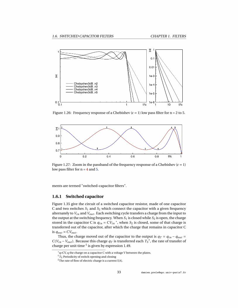
Chebyshev frequency response
Figure 1.26 shows the ripple in the pass-band of a Chebyshev low pass filter (3dB)for order from 2 to 5. It also appears that H0 (numerator) is different from 1 foreven order. For an even order Chebyshev filter with a ripple factor of 3 dB (whichcorrespond to ε= 1), the numerator is equal to 1p
1+ε2≈ 0.71.
Figure 1.27 shows more precisely the difference in H0 between odd (n=5 → H0 =1) and even (n=4 → H0 ≈ 0.707) order. It also illustrates of how it is possible to de-termine the order of a Chebyshev filter by simply counting the ripple number on thetransfer function.
Amplitudes of the ripples in the pass-band is constrained by the |H |max − Amax
and fc (Fig. 1.21). Sometimes, ripple factor needs to be smaller than 3dB. It is easyto find Chebyshev polynomials table with a ripple factor of 1 dB*, 0.5 dB or 0.1 dB.In Figure 1.29, is plotted the transfer function of a Chebyshev low-pass filter with a
*Chebyshev polynomials table is given in Appendix A for a ripple factor of 3 and 1 dB

1.6. SWITCHED CAPACITOR FILTERS CHAPTER 1. FILTERS
Figure 1.25: Frequency response of a Butterworth low pass filter for n = 2 to 5.
ripple factor of 1 dB (ε= 0.5) and order going from 2 to 5. The H0 of even order is setat 1p
1+0.52≈ 0.894 as it is shown in figure 1.29.
Finally, a comparison between two Chebishev low pass filters with different rip-ple factor is plotted in figure 1.30. Even if the cutoff frequency is referred to a differ-ent level (-1 dB and -3 dB), it appears that the larger the ripple factor, the faster therolloff.
Bessel frequency response
Figure 1.31 show Bessel low pass filter transfer function from the 2nd to the 5th order.The rolloff is much slower than for other filters. Indeed, Bessel filter maximizes theflatness of the group delay curve in the passband (Fig. 1.32) but not the rolloff. So,for a same attenuation in the stop band (Ami n), a higher order is required comparedto Butterworth, Chebyshev or Legendre filter.
Legendre frequency response
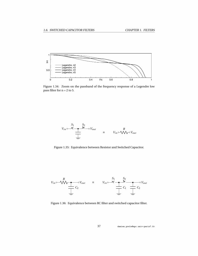
To complete this inventory, Legendre low-pass filter frequency response is plottedin figure 1.33 for n = 2 to 5.
Legendre filter is characterized by the maximum possible rolloff consistent withmonotonic magnitude response in the pass band. But monotonic does not flat, aswe can see in figure 1.34.
As for Chebyshev filter, it is possible to count the number of "ripples" to find theorder from a plotted transfer function.
1.6 Switched capacitor filters
A switched capacitor electronic circuit works by moving charges into and out of ca-pacitors when switches are opened and closed. Filters implemented with these ele-
1.6. SWITCHED CAPACITOR FILTERS CHAPTER 1. FILTERS
Figure 1.26: Frequency response of a Chebishev (ε= 1) low pass filter for n = 2 to 5.
Figure 1.27: Zoom in the passband of the frequency response of a Chebishev (ε= 1)low pass filter for n = 4 and 5.
ments are termed "switched-capacitor filters".
1.6.1 Switched capacitor
Figure 1.35 give the circuit of a switched capacitor resistor, made of one capacitorC and two switches S1 and S2 which connect the capacitor with a given frequencyalternately to Vi n and Vout . Each switching cycle transfers a charge from the input tothe output at the switching frequency. When S1 is closed while S2 is open, the chargestored in the capacitor C is qi n = CVi n *, when S2 is closed, some of that charge istransferred out of the capacitor, after which the charge that remains in capacitor Cis qout =CVout .
Thus, the charge moved out of the capacitor to the output is qT = qi n − qout =C (Vi n −Vout ). Because this charge qT is transferred each TS
†, the rate of transfer ofcharge per unit time ‡ is given by expression 1.49.
*q=CV, q the charge on a capacitor C with a voltage V between the plates.†TS Periodicity of switch opening and closing‡The rate of flow of electric charge is a current I[A].
1.6. SWITCHED CAPACITOR FILTERS CHAPTER 1. FILTERS
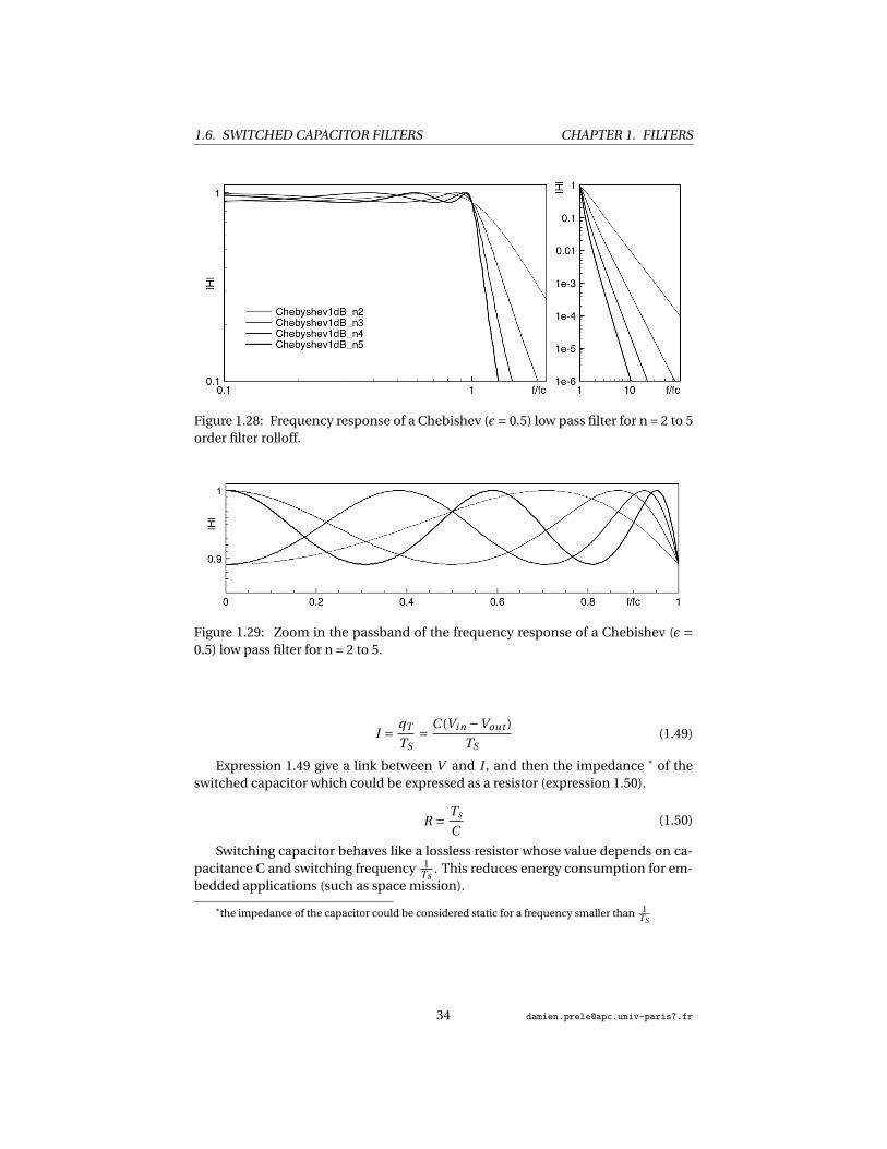
Figure 1.28: Frequency response of a Chebishev (ε= 0.5) low pass filter for n = 2 to 5order filter rolloff.
Figure 1.29: Zoom in the passband of the frequency response of a Chebishev (ε =0.5) low pass filter for n = 2 to 5.
I = qT
TS= C (Vi n −Vout )
TS(1.49)
Expression 1.49 give a link between V and I , and then the impedance * of theswitched capacitor which could be expressed as a resistor (expression 1.50).
R = Ts
C(1.50)
Switching capacitor behaves like a lossless resistor whose value depends on ca-pacitance C and switching frequency 1
TS. This reduces energy consumption for em-
bedded applications (such as space mission).
*the impedance of the capacitor could be considered static for a frequency smaller than 1TS

1.6. SWITCHED CAPACITOR FILTERS CHAPTER 1. FILTERS
Figure 1.30: Comparison between frequency response of two Chebishev low passfilters of 5th order, one with a ripple factor of 1 dB, and the other with 3 dB.
1.6.2 Switched capacitor filters
Because switching capacitor act as a resistor, switched capacitors can be used in-stead of resistors in the previous filter circuits (RC, RLC, Sallen-Key ...). A R = 10kΩcan be replaced by a switched capacitor following the expression 1.50. Using a switch-ing clock fs = 1
TS= 50kH z, the capacitor is given by equation 1.51.
R = 10kΩ ≡ C = 1
10kΩ×50kH z= 2nF (1.51)
A variation of the switching frequency leads to a variation of the equivalent resis-tance R. If fs increases, R = 1
C× fsdecreases. This link between frequency and equiv-
alent resistance value could be used to modify a filter cutoff frequency by adjustingthe switching frequency.
The cutoff frequency of a RC switched capacitor filter (Fig. 1.36) is expressed byequation 1.52.
fc = 1
2πRequi v.C2= C1 × fs
2πC2(1.52)
If the switching frequency fs increases, the cutoff frequency fc increases also.

1.6. SWITCHED CAPACITOR FILTERS CHAPTER 1. FILTERS
Figure 1.31: Frequency response of a Bessel low pass filter for n = 2 to 5.
Figure 1.32: Comparison of the delay time as a function of frequency ( ffc
) betweena Bessel, a Butterworth and a Chebyshev low-pass filter (n=4).
Figure 1.33: Frequency response of a Legendre low pass filter for n = 2 to 5
1.6. SWITCHED CAPACITOR FILTERS CHAPTER 1. FILTERS
Figure 1.34: Zoom on the passband of the frequency response of a Legendre lowpass filter for n = 2 to 5.
Vi n
RVout≡
Vi n
S1 S2
Vout
Figure 1.35: Equivalence between Resistor and Switched Capacitor.
Vi n
RVout
C2
≡ Vi n
S1 S2
Vout
C2C1
Figure 1.36: Equivalence between RC filter and switched capacitor filter.
CHAPTER 2DC/DC CONVERTERS
2.1 Introduction
A DC/DC converter is an electronic circuit which converts a DC (Direct Current)source from one voltage level to another. Power for a DC/DC converter can
come from any suitable DC sources, such as batteries, solar panels, rectifiers andDC generators.
DC/DC converter is a class of switched-mode power supply containing at leasttwo semiconductor switches (a diode and a transistor) and at least one energy stor-age element, a capacitor, inductor, or the two in combination. Filters made of capac-itors (sometimes in combination with inductors) are normally added to the outputof the converter to reduce output voltage ripple.
2.1.1 Advantages/Disadvantages
Pros :
DC/DC converters offer three main advantages compared to linear regulators :
1. Efficiency : Switching power supplies offer higher efficiency than traditionallinear power supplies*. Unlike a linear power supply, the pass transistor ofa switching-mode supply continually switches between low-dissipation, full-on and full-off states †, and spends very little time in transitions to minimizewasted energy. Ideally, a switched mode power supply dissipates no power.This higher efficiency is an important advantage of a switched mode powersupply.
*A linear power supply regulates the output voltage by continually dissipating power (Joule dissipa-tion) in a pass transistor (made to act like a variable resistor). The lost power is Plost = (Vout −Vi n )Il oad .
†A switching regulator uses an active device that switches "on" and "off" to maintain an averagevalue of output.
38
2.2. DC/DC CONVERTERS CHAPTER 2. DC/DC CONVERTERS
2. Size : Switched mode power supplies may also be substantially smaller andlighter than a linear supply due to the smaller transformer size and weight;and due to the less thermal management required because less energy is lostin the transfer.
3. Output voltages can be greater than the input or negative : DC/DC convertercan transform input voltage to output voltages that can be greater than theinput (boost), negative (inverter), or can even be transferred through a trans-former to provide electrical isolation with respect to the input. By contrastlinear regulator can only generate a lower voltage value than input one.
Cons :
However, DC/DC converter are more complicated ; their switching currents cancause electrical noise problems if not carefully suppressed*. Linear regulators pro-vide lower noise ; their simplicity can sometimes offer a less expensive solution.Even if the most of low noise electronic circuits can tolerate some of the less-noisyDC/DC converters, some sensitive analog circuits require a power supply with solittle noise that it can only be provided by a linear regulator.
2.1.2 Applications
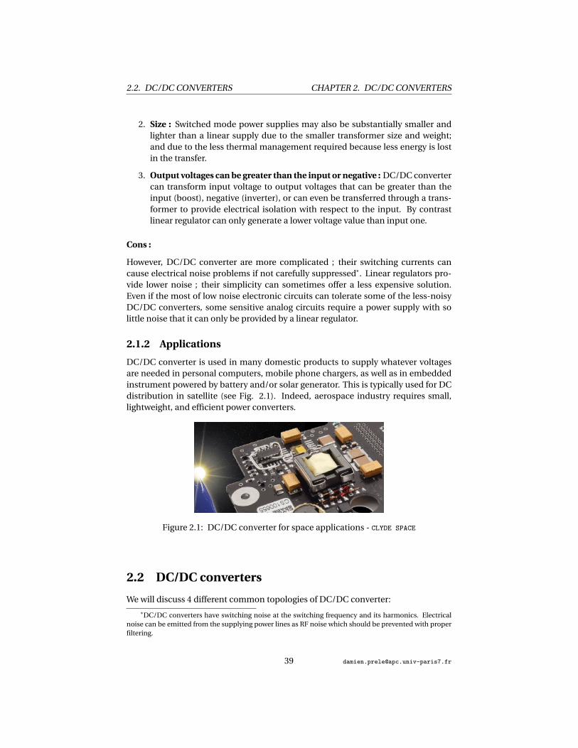
DC/DC converter is used in many domestic products to supply whatever voltagesare needed in personal computers, mobile phone chargers, as well as in embeddedinstrument powered by battery and/or solar generator. This is typically used for DCdistribution in satellite (see Fig. 2.1). Indeed, aerospace industry requires small,lightweight, and efficient power converters.
Figure 2.1: DC/DC converter for space applications - CLYDE SPACE
2.2 DC/DC converters
We will discuss 4 different common topologies of DC/DC converter:
*DC/DC converters have switching noise at the switching frequency and its harmonics. Electricalnoise can be emitted from the supplying power lines as RF noise which should be prevented with properfiltering.
2.2. DC/DC CONVERTERS CHAPTER 2. DC/DC CONVERTERS
1. step-down voltage converter ⇒ buck converter.
2. step-up voltage converter ⇒ boost converter.
3. inverter voltage converter ⇒ inverting buck-boost converter.
4. isolated* voltage converter ⇒ flyback converter.
2.2.1 Buck converters
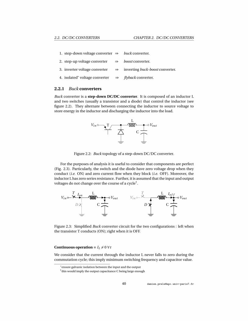
Buck converter is a step-down DC/DC converter. It is composed of an inductor Land two switches (usually a transistor and a diode) that control the inductor (seefigure 2.2). They alternate between connecting the inductor to source voltage tostore energy in the inductor and discharging the inductor into the load.
Vi n TL
C
Vout
Figure 2.2: Buck topology of a step-down DC/DC converter.
For the purposes of analysis it is useful to consider that components are perfect(Fig. 2.3). Particularly, the switch and the diode have zero voltage drop when theyconduct (i.e. ON) and zero current flow when they block (i.e. OFF). Moreover, theinductor L has zero series resistance. Further, it is assumed that the input and outputvoltages do not change over the course of a cycle†.
Vi nIon
T L
C
Vout
D
Vi n
T L Io f f
C
Vout
D
Figure 2.3: Simplified Buck converter circuit for the two configurations : left whenthe transistor T conducts (ON); right when it is OFF.
Continuous operation ≡ IL 6= 0 ∀t
We consider that the current through the inductor L never falls to zero during thecommutation cycle; this imply minimum switching frequency and capacitor value.
*ensure galvanic isolation between the input and the output†this would imply the output capacitance C being large enough
2.2. DC/DC CONVERTERS CHAPTER 2. DC/DC CONVERTERS
Charge phase TON : When the transistor conducts (diode is reverse biased), thevoltage across the inductor (VL =Vi n −Vout ) is considered as a constant voltage to afirst approximation. So the current through the inductor IL rises linearly with timefollowing expression 2.1 with a VL
L slope*.
dIL = 1
L
∫t=TON
VLdt (2.1)
During the charge phase TON , IL increase by the value∆ILON given by expression2.2.
∆ILON = Vi n −Vout
LTON (2.2)
Discharge phase TOF F : When the transistor is no longer biased (i.e. OFF), diodeis forward biased and conducts. The voltage across the inductor becomes equal to−Vout
† and IL flows to the load through the diode. IL decrease by the value ∆ILOF F
given by expression 2.3 due to the linear discharge of the inductor.
∆ILOF F = −Vout
LTOF F (2.3)
Entire switching cycle : In a steady-state operation condition, IL at t = 0 is equal toIL at t = T = TON +TOF F . So the increase of IL during TON is equal‡ to the decreasingduring TOF F .
∆ILON +∆ILOF F = 0 (2.4)
We can then establish the relationship 2.5 which allows to obtains the conversionfactor between Vi n and Vout as a function of the duty cycle D = TON
T . It appears thatVout varies linearly with the duty cycle for a given Vi n .
(Vi n −Vout )TON −Vout TOF F = 0 −−−−−−−−−−→D= TON
TON +TOF F
Vout = DVi n (2.5)
As the duty cycle D is equal to the ratio between TON and the period T, it cannotbe more than 1. Therefore, Vout ≤ Vi n . This is why this converter is named a step-down converter.
Figure 2.4 shows the evolution of voltage and current of an ideal buck converterduring charge and discharge phases.
2.2.2 Boost converters
A boost converter (step-up converter) is a DC/DC converter with an output voltagevalue greater than its input voltage value. The key principle that drives the boost
*We consider here the current charge of the inductor. The capacitor is assumed charge at a constantvoltage.
†Voltage drop across diode is neglected.‡in absolute value, but not in sign.
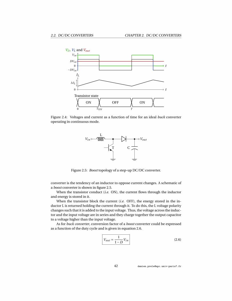
2.2. DC/DC CONVERTERS CHAPTER 2. DC/DC CONVERTERS
0 t
VD , VL and Vout
Vi n
DVi n
−DVi n
0 t
IL
∆IL
Transistor state
ON OFF ON
0 TON T
Figure 2.4: Voltages and current as a function of time for an ideal buck converteroperating in continuous mode.
Vi n
L
C
Vout
T
Figure 2.5: Boost topology of a step-up DC/DC converter.
converter is the tendency of an inductor to oppose current changes. A schematic ofa boost converter is shown in figure 2.5.
When the transistor conduct (i.e. ON), the current flows through the inductorand energy is stored in it.
When the transistor block the current (i.e. OFF), the energy stored in the in-ductor L is returned holding the current through it. To do this, the L voltage polaritychanges such that it is added to the input voltage. Thus, the voltage across the induc-tor and the input voltage are in series and they charge together the output capacitorto a voltage higher than the input voltage.
As for buck converter, conversion factor of a boost converter could be expressedas a function of the duty cycle and is given in equation 2.6.
Vout = 1
1−DVi n (2.6)
2.2. DC/DC CONVERTERS CHAPTER 2. DC/DC CONVERTERS
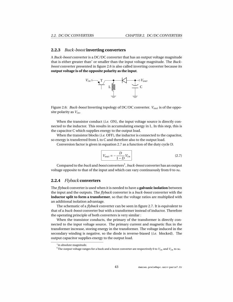
2.2.3 Buck-boost inverting converters
A Buck-boost converter is a DC/DC converter that has an output voltage magnitudethat is either greater than* or smaller than the input voltage magnitude. The Buck-boost converter presented in figure 2.6 is also called inverting converter because itsoutput voltage is of the opposite polarity as the input.
Vi n T
C
Vout
L
Figure 2.6: Buck-boost Inverting topology of DC/DC converter. Vout is of the oppo-site polarity as Vi n .
When the transistor conduct (i.e. ON), the input voltage source is directly con-nected to the inductor. This results in accumulating energy in L. In this step, this isthe capacitor C which supplies energy to the output load.
When the transistor blocks (i.e. OFF), the inductor is connected to the capacitor,so energy is transferred from L to C and therefore also to the output load.
Conversion factor is given in equation 2.7 as a function of the duty cycle D.
Vout =− D
1−DVi n (2.7)
Compared to the buck and boost converters†, buck-boost converter has an outputvoltage opposite to that of the input and which can vary continuously from 0 to ∞.
2.2.4 Flyback converters
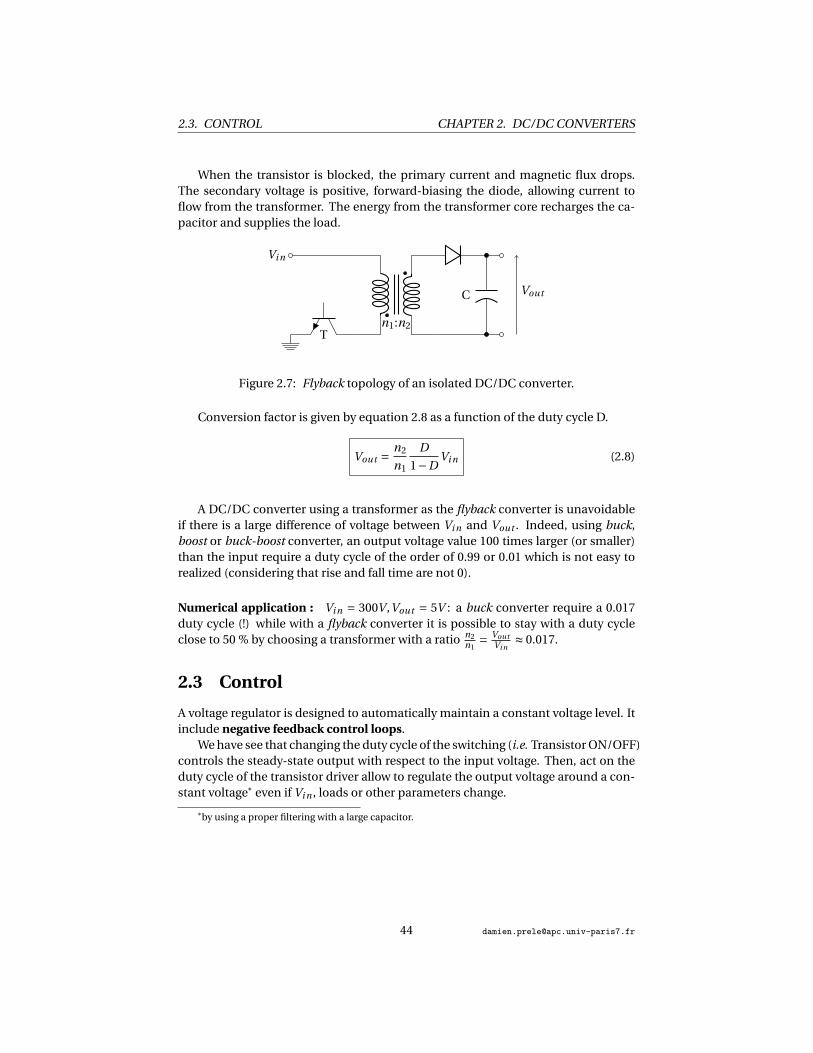
The flyback converter is used when it is needed to have a galvanic isolation betweenthe input and the outputs. The flyback converter is a buck-boost converter with theinductor split to form a transformer, so that the voltage ratios are multiplied withan additional isolation advantage.
The schematic of a flyback converter can be seen in figure 2.7. It is equivalent tothat of a buck-boost converter but with a transformer instead of inductor. Thereforethe operating principle of both converters is very similar :
When the transistor conducts, the primary of the transformer is directly con-nected to the input voltage source. The primary current and magnetic flux in thetransformer increase, storing energy in the transformer. The voltage induced in thesecondary winding is negative, so the diode is reverse-biased (i.e. blocked). Theoutput capacitor supplies energy to the output load.
*in absolute magnitude.†The output voltage ranges for a buck and a boost converter are respectively 0 to Vi n and Vi n to ∞.
2.3. CONTROL CHAPTER 2. DC/DC CONVERTERS
When the transistor is blocked, the primary current and magnetic flux drops.The secondary voltage is positive, forward-biasing the diode, allowing current toflow from the transformer. The energy from the transformer core recharges the ca-pacitor and supplies the load.
Vi n
Tn1:n2
C Vout
Figure 2.7: Flyback topology of an isolated DC/DC converter.
Conversion factor is given by equation 2.8 as a function of the duty cycle D.
Vout = n2
n1
D
1−DVi n (2.8)
A DC/DC converter using a transformer as the flyback converter is unavoidableif there is a large difference of voltage between Vi n and Vout . Indeed, using buck,boost or buck-boost converter, an output voltage value 100 times larger (or smaller)than the input require a duty cycle of the order of 0.99 or 0.01 which is not easy torealized (considering that rise and fall time are not 0).
Numerical application : Vi n = 300V ,Vout = 5V : a buck converter require a 0.017duty cycle (!) while with a flyback converter it is possible to stay with a duty cycleclose to 50 % by choosing a transformer with a ratio n2
n1= Vout
Vi n≈ 0.017.
2.3 Control
A voltage regulator is designed to automatically maintain a constant voltage level. Itinclude negative feedback control loops.
We have see that changing the duty cycle of the switching (i.e. Transistor ON/OFF)controls the steady-state output with respect to the input voltage. Then, act on theduty cycle of the transistor driver allow to regulate the output voltage around a con-stant voltage* even if Vi n , loads or other parameters change.
*by using a proper filtering with a large capacitor.
2.3. CONTROL CHAPTER 2. DC/DC CONVERTERS
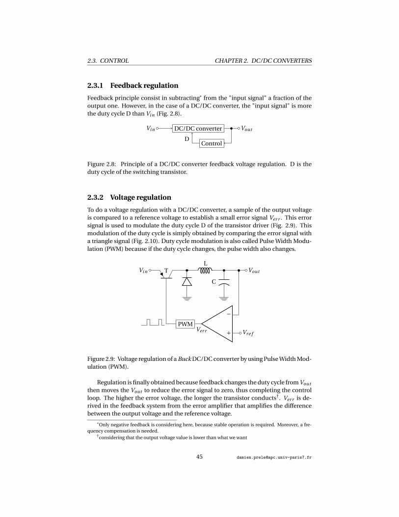
2.3.1 Feedback regulation
Feedback principle consist in subtracting* from the "input signal" a fraction of theoutput one. However, in the case of a DC/DC converter, the "input signal" is morethe duty cycle D than Vi n (Fig. 2.8).
VoutVi n
D
DC/DC converter
Control
Figure 2.8: Principle of a DC/DC converter feedback voltage regulation. D is theduty cycle of the switching transistor.
2.3.2 Voltage regulation
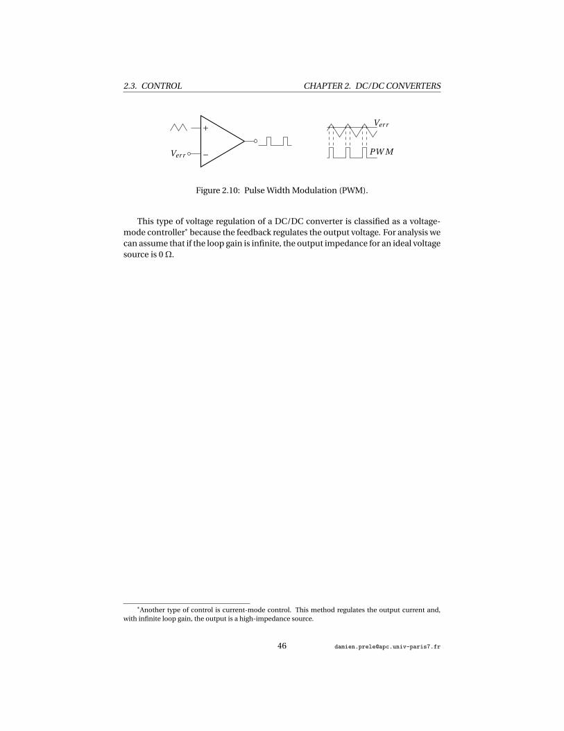
To do a voltage regulation with a DC/DC converter, a sample of the output voltageis compared to a reference voltage to establish a small error signal Ver r . This errorsignal is used to modulate the duty cycle D of the transistor driver (Fig. 2.9). Thismodulation of the duty cycle is simply obtained by comparing the error signal witha triangle signal (Fig. 2.10). Duty cycle modulation is also called Pulse Width Modu-lation (PWM) because if the duty cycle changes, the pulse width also changes.
Vi n TL
C
Vout
−
+Ver r Vr e f
PWM
Figure 2.9: Voltage regulation of a Buck DC/DC converter by using Pulse Width Mod-ulation (PWM).
Regulation is finally obtained because feedback changes the duty cycle from Vout
then moves the Vout to reduce the error signal to zero, thus completing the controlloop. The higher the error voltage, the longer the transistor conducts†. Ver r is de-rived in the feedback system from the error amplifier that amplifies the differencebetween the output voltage and the reference voltage.
*Only negative feedback is considering here, because stable operation is required. Moreover, a fre-quency compensation is needed.
†considering that the output voltage value is lower than what we want
2.3. CONTROL CHAPTER 2. DC/DC CONVERTERS
−
+
Ver r
Ver r
PW M
Figure 2.10: Pulse Width Modulation (PWM).
This type of voltage regulation of a DC/DC converter is classified as a voltage-mode controller* because the feedback regulates the output voltage. For analysis wecan assume that if the loop gain is infinite, the output impedance for an ideal voltagesource is 0Ω.
*Another type of control is current-mode control. This method regulates the output current and,with infinite loop gain, the output is a high-impedance source.

CHAPTER 3PHASE LOCKED LOOP
3.1 Introduction
THE Phase Locked Loop (PLL) plays an important role in modern electronic andparticularly for space communications. Indeed, PLL is a crucial part of modula-
tor, demodulator or synchronization systems. As example of space application (Fig.3.1), PLL is particularly essential to estimate the instantaneous phase of a receivedsignal, such as carrier tracking from Global Positioning System (GPS) satellites.
Figure 3.1: PLLs used for space applications (Peregrine Semiconductor); GPS constella-tion around the Earth.
PLL allows to extract signals from noisy transmission channels. Indeed, commu-nications between satellites and ground stations are usually buried in atmosphericnoise or some type of interferences (frequency selective fading* or doppler shift†)which one manage by a PLL.
PLL circuits can also be used to distribute clock signal, or set up as frequencymultipliers or dividers for frequency synthesis.
*Frequency selective fading : Radio signal arrives at the receiver by two different paths.†Doppler shift : Shift in frequency for a receiver moving relative to the emitter
47
3.2. DESCRIPTION CHAPTER 3. PHASE LOCKED LOOP
3.2 Description
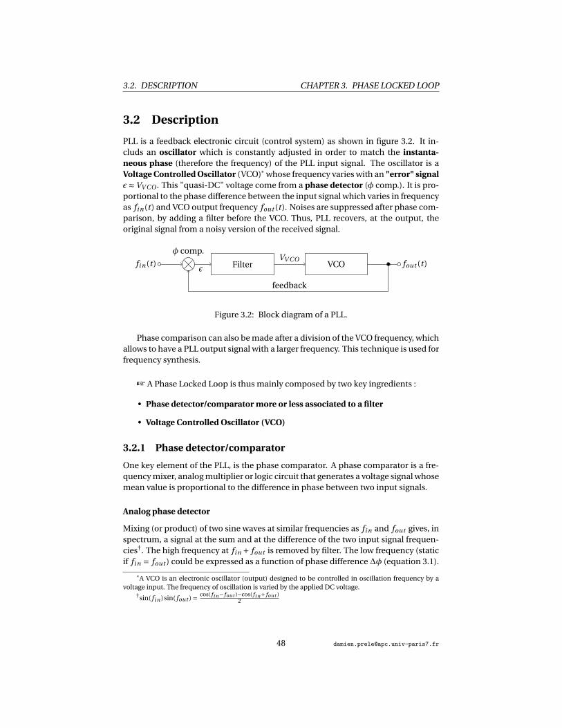
PLL is a feedback electronic circuit (control system) as shown in figure 3.2. It in-cluds an oscillator which is constantly adjusted in order to match the instanta-neous phase (therefore the frequency) of the PLL input signal. The oscillator is aVoltage Controlled Oscillator (VCO)* whose frequency varies with an "error" signalε≈VV CO . This "quasi-DC" voltage come from a phase detector (φ comp.). It is pro-portional to the phase difference between the input signal which varies in frequencyas fi n(t ) and VCO output frequency fout (t ). Noises are suppressed after phase com-parison, by adding a filter before the VCO. Thus, PLL recovers, at the output, theoriginal signal from a noisy version of the received signal.
fi n(t )
φ comp.
FilterεVCO fout (t )
feedback
VV CO
Figure 3.2: Block diagram of a PLL.
Phase comparison can also be made after a division of the VCO frequency, whichallows to have a PLL output signal with a larger frequency. This technique is used forfrequency synthesis.
+ A Phase Locked Loop is thus mainly composed by two key ingredients :
• Phase detector/comparator more or less associated to a filter
• Voltage Controlled Oscillator (VCO)
3.2.1 Phase detector/comparator
One key element of the PLL, is the phase comparator. A phase comparator is a fre-quency mixer, analog multiplier or logic circuit that generates a voltage signal whosemean value is proportional to the difference in phase between two input signals.
Analog phase detector
Mixing (or product) of two sine waves at similar frequencies as fi n and fout gives, inspectrum, a signal at the sum and at the difference of the two input signal frequen-cies†. The high frequency at fi n + fout is removed by filter. The low frequency (staticif fi n = fout ) could be expressed as a function of phase difference ∆φ (equation 3.1).
*A VCO is an electronic oscillator (output) designed to be controlled in oscillation frequency by avoltage input. The frequency of oscillation is varied by the applied DC voltage.
†sin( fi n )sin( fout ) = cos( fi n− fout )−cos( fi n+ fout )2
3.2. DESCRIPTION CHAPTER 3. PHASE LOCKED LOOP
sin(2π fi n t +φi n
)× sin(2π fout t +φout
)∝ cos
(∆φ
)︸ ︷︷ ︸static
−cos(2π( fi n + fout )t +φi n +φout
)︸ ︷︷ ︸filtered signal
(3.1)
So multiplication allows to detect phase difference between two sine waves. Thisis why phase comparator is currently represented by the symbol
⊗as in figure 3.2.
Digital phase detector
Phase locked loop device as the popular CD4046 integrated circuit include two kindof digital phase comparators :
• Type I phase comparator is designed to be driven by analog signals or square-wave digital signals and produces an output pulse at twice the input frequency.It produces an output waveform, which must be filtered to drive the VCO.
• Type II phase comparator is sensitive only to the relative timing of the edges ofthe inputs. In steady state (both signals are at the same frequency), it producesa constant output voltage proportional to the phase difference. This outputwill tend not to produce ripple in the control voltage of the VCO.
Type I phase detector : XOR The simplest phase comparator is the eXclusiveOR (XOR) gate. A XOR gate is a digital logic gate which compute the binary addition*
which is symbolized by⊕
. XOR truth table is shown in figure 3.1.
A B A ⊕ B0 0 00 1 11 0 11 1 0
Table 3.1: XOR truth table.
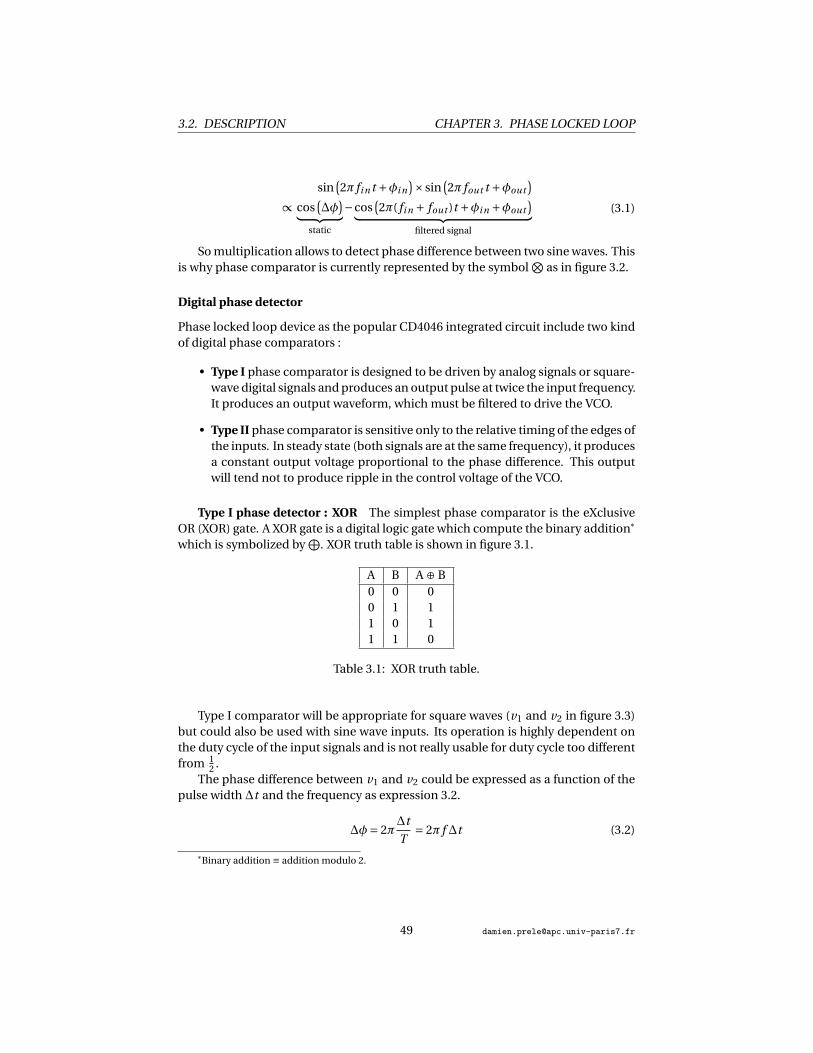
Type I comparator will be appropriate for square waves (v1 and v2 in figure 3.3)but could also be used with sine wave inputs. Its operation is highly dependent onthe duty cycle of the input signals and is not really usable for duty cycle too differentfrom 1
2 .The phase difference between v1 and v2 could be expressed as a function of the
pulse width ∆t and the frequency as expression 3.2.
∆φ= 2π∆t
T= 2π f ∆t (3.2)
*Binary addition ≡ addition modulo 2.
3.2. DESCRIPTION CHAPTER 3. PHASE LOCKED LOOP
v1(t )
v2(t )vout (t )
v1(t )
v2(t )
vout (t )
T
∆t0V
Vdd
Figure 3.3: XOR phase comparator.
For a duty cycle = 12 , XOR produces pulse train with twice the frequency of v1 and
v2. This periodic square wave signal vout has a duty cycle Dvout given by expression3.3, function of input phase difference ∆φ.
Dvout =∆φ
π(3.3)
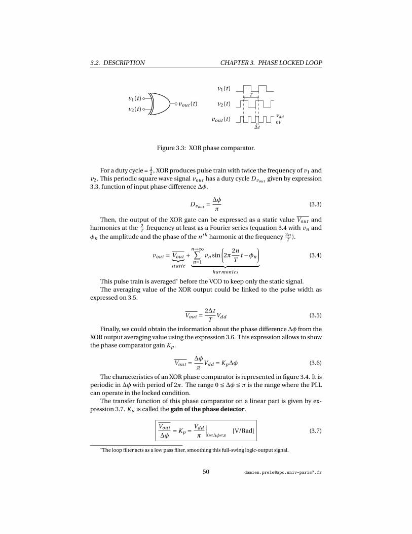
Then, the output of the XOR gate can be expressed as a static value Vout andharmonics at the 2
T frequency at least as a Fourier series (equation 3.4 with vn and
φn the amplitude and the phase of the nth harmonic at the frequency 2nT ).
vout = Vout︸︷︷︸st ati c
+n→∞∑n=1
vn sin
(2π
2n
Tt −φn
)︸ ︷︷ ︸
har moni cs
(3.4)
This pulse train is averaged* before the VCO to keep only the static signal.The averaging value of the XOR output could be linked to the pulse width as
expressed on 3.5.
Vout = 2∆t
TVdd (3.5)
Finally, we could obtain the information about the phase difference∆φ from theXOR output averaging value using the expression 3.6. This expression allows to showthe phase comparator gain Kp .
Vout = ∆φπ
Vdd = Kp∆φ (3.6)
The characteristics of an XOR phase comparator is represented in figure 3.4. It isperiodic in ∆φ with period of 2π. The range 0 ≤ ∆φ ≤ π is the range where the PLLcan operate in the locked condition.
The transfer function of this phase comparator on a linear part is given by ex-pression 3.7. Kp is called the gain of the phase detector.
Vout
∆φ= Kp = Vdd
π
∣∣∣0≤∆φ≤π [V/Rad] (3.7)
*The loop filter acts as a low pass filter, smoothing this full-swing logic-output signal.

3.2. DESCRIPTION CHAPTER 3. PHASE LOCKED LOOP
0
Vout
∆φ
π 2ππ2
Vdd2
VddKp
Figure 3.4: Periodic characteristic of an XOR phase comparator and a typical oper-ating point. The slope Kp is the gain of the comparator.
When PLL is in lock with this type of comparator, the steady-state phase differ-ence at the inputs is near π
2 .So, this kind of phase comparator generate always an output "digital" signal in
the PLL loop. Therefore, despite low pass filter, it always remain residual ripples,and consequent periodic phase variations.
Type II phase detector : charge pump By contrast to the type I comparator,the type II phase detector generates output pulses only when there is a phase errorbetween the input and the VCO signal.
• If the two input are in phase : The phase detector looks like an open circuitand the loop filter capacitor then acts as a voltage-storage device, holding thevoltage that gives the VCO frequency.
• If the input signal moves away in frequency : The phase detector generatesa train of short pulses*, charging the capacitor of the filter to the new voltageneeded to keep the VCO locked.
So, the output pulses disappear entirely when the two signals are in lock†. Thismeans that there is no ripple present at the output to generate periodic phase mod-ulation in the loop, as there is with the type I phase detector.
3.2.2 Voltage Control Oscillator - VCO
The other key ingredient of the PLL, is the VCO. It exist two different types of con-trolled oscillators :
• Resonant/Harmonic oscillators (> 50 MHz)
• Relaxation oscillators (< 50 MHz)
*The short pulses contain very little energy and are easy to filter out of the VCO control voltage. Thisresults in low VCO control line ripple and therefore low frequency modulation on the VCO.
†A charge pump phase detector must always have a "dead frequency band" where the phases of in-puts are close enough that the comparator detects no phase error. So, charge pump introduce necessarilya significant peak-to-peak jitter, because of drift within the dead frequency band.

3.2. DESCRIPTION CHAPTER 3. PHASE LOCKED LOOP
For microwave applications, resonant oscillators implemented with devices asLC tank circuit is used. C value is adjusted (tuning) thanks to a varactor diode.
Howevere, we will concentrate on non-microwave applications, and thus on therelaxation oscillators more easily implementable on integrated circuit. This is typi-cally the VCO that we can find in the CD4046 PLL integrated circuit. VV CO controlsthe charging and discharging currents through an external* capacitor C , and there-fore determines the time needed to charge and discharge the capacitor to a pre-determined threshold level. As a result, the frequency fV CO changes as a function ofVV CO .
If VV CO evolves, a linear VCO transfer function can be expressed as equation 3.8.
fmax − fmi n
Vmax −Vmi n= K0 [Hz/V] (3.8)
In practice Vmax is limited by VDD and Vmi n by 0V (or VSS ). Assuming a linearresponse as in figure 3.5, fmax and fmi n are adjusted and therefore fix the gain K0.
0
VV CO
0fV CO
fmi n fmaxf0
1K0
Vdd
Vdd2
Figure 3.5: VCO characteristic : VV CO as a function of fV CO .
The VCO transfer function can also be expressed using the angular frequencyωV CO (eq. 3.9).
ωV CO
VV CO= 2πK0 = Kv [rad/V.s] (3.9)
The VCO gain is generally expressed as a radian frequency per voltage; so its unitsare rad/V.s even if the "rad" is often omitted.
However, for a PLL, the phase instead of frequency is interesting. It is then moreuseful to express the phase output of the VCO :∫
ωV CO(t )dt =φV CO(t ) → ωV CO(s)
s=φV CO(s) (3.10)
Then the transfer function between the phase and the input voltage of the VCOis given by expression 3.11
φV CO(s)
VV CO(s)= Kv
s(3.11)
*not implemented on the CD4046 to allow tuning of the fV CO0 center frequency.

3.3. FREQUENCY RANGE CHAPTER 3. PHASE LOCKED LOOP
3.3 Frequency range
Operating frequency range of a PLL is graphically represented in figure 3.6. Twomain frequency ranges appear :
• Lock range
• Capture range
fi nf0f0 −∆ fCf0 −∆ fL ≈ fmi n f0 +∆ fC f0 +∆ fL ≈ fmax
Lock range / hold range
Pull-inPull-in Operating range
Capture range
Dynamically unstable Unconditionally unstableConditionally stable
Figure 3.6: Scope of the 2 main frequency ranges of a PLL : Lock (or Hold) range andCapture range (more or less defines due to pull-in effect).
3.3.1 Lock range
The Lock range (also called Hold range) is the frequency range in which a PLL is ableto stay locked. It correspond to a "static stable frequency range"; this means thatthe PLL remains locked if the input signal is a fixed frequency signal comprised inthis range.
The Lock range is mainly defined by the VCO range.Figure 3.4 shows that when the phase comparator is used on a PLL, the phase
difference ∆φ need to be small enough to stay on a linear regime. So, VCO is usedto operate around a center frequency fV CO0 = f0 and around VV CO0 = Vdd
2* as it is
represented in figure 3.5. Then, ∆φmax = π around this operating point (eq. 3.12and Fig. 3.4).
0 ≤∆φ≤π (3.12)
Knowing that ∆φ must be included in [0;π] range, we can expressed the maxi-mum range in frequency at the output of the VCO as equation 3.13 (from Fig. 3.5 →fmax − fmi n = K0Vdd and Fig. 3.4 → Vdd =πKp ).
fmax − fmi n =πK0Kp = Kv Kp
2(3.13)
From this expression, lock range 2∆ fL = fmax − fmi n is defined as equation 3.14.
*In this operating point, the two compared signals are in quadrature.
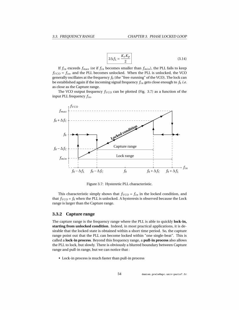
3.3. FREQUENCY RANGE CHAPTER 3. PHASE LOCKED LOOP
2∆ fL = Kv Kp
2(3.14)
If fi n exceeds fmax (or if fi n becomes smaller than fmi n), the PLL fails to keepfV CO = fi n , and the PLL becomes unlocked. When the PLL is unlocked, the VCOgenerally oscillates at the frequency f0 (the "free-running" of the VCO). The lock canbe established again if the incoming signal frequency fi n gets close enough to f0 i.e.as close as the Capture range.
The VCO output frequency fV CO can be plotted (Fig. 3.7) as a function of theinput PLL frequency fi n .
fi nf0f0 −∆ fCf0 −∆ fL f0 +∆ fC f0 +∆ fL
Capture range
Lock range
fV CO
f0
fmax
f0 +∆ fC
f0 −∆ fC
fmi n
Locked condition
Figure 3.7: Hysteretic PLL characteristic.
This characteristic simply shows that fV CO = fi n in the locked condition, andthat fV CO = f0 when the PLL is unlocked. A hysteresis is observed because the Lockrange is larger than the Capture range.
3.3.2 Capture range
The capture range is the frequency range where the PLL is able to quickly lock-in,starting from unlocked condition. Indeed, in most practical applications, it is de-sirable that the locked state is obtained within a short time period. So, the capturerange point out that the PLL can become locked within "one single-beat". This iscalled a lock-in process. Beyond this frequency range, a pull-in process also allowsthe PLL to lock, but slowly. There is obviously a blurred boundary between Capturerange and pull-in range, but we can notice that :
• Lock-in process is much faster than pull-in process
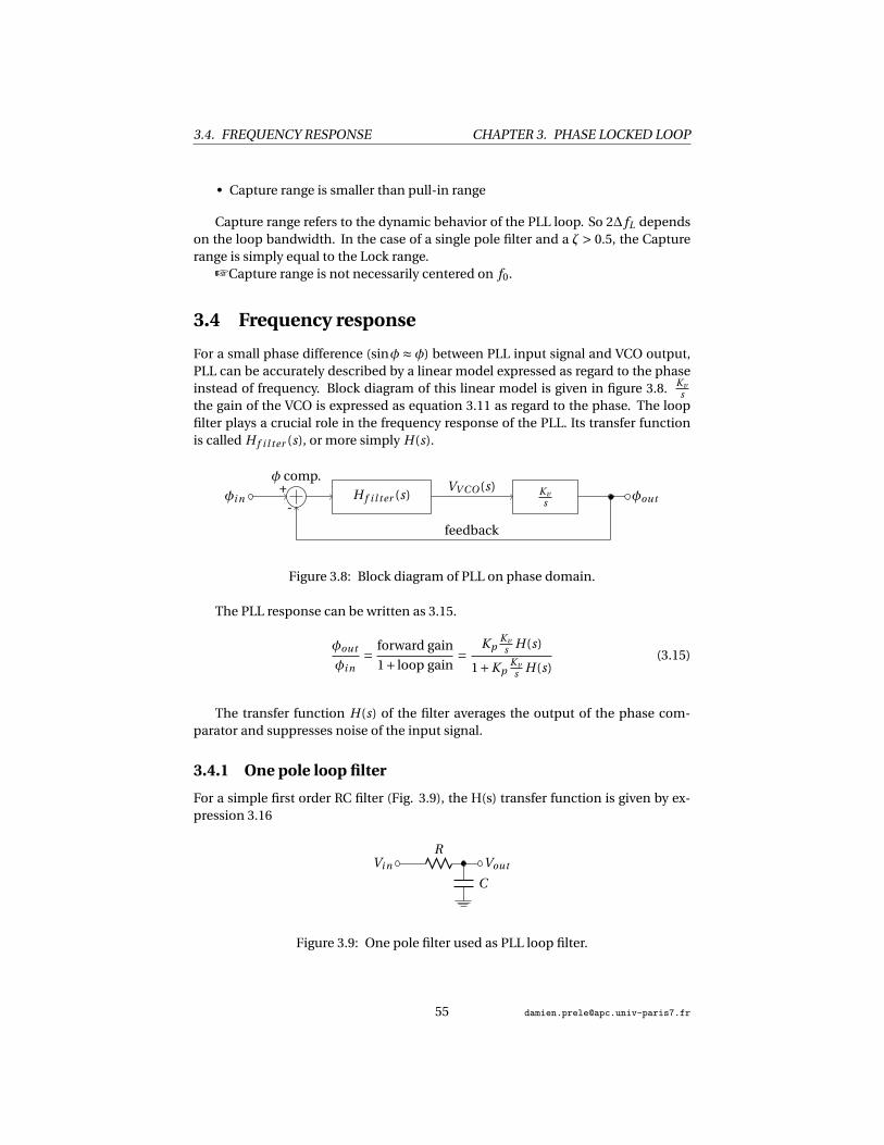
3.4. FREQUENCY RESPONSE CHAPTER 3. PHASE LOCKED LOOP
• Capture range is smaller than pull-in range
Capture range refers to the dynamic behavior of the PLL loop. So 2∆ fL dependson the loop bandwidth. In the case of a single pole filter and a ζ > 0.5, the Capturerange is simply equal to the Lock range.
+Capture range is not necessarily centered on f0.
3.4 Frequency response
For a small phase difference (sinφ ≈ φ) between PLL input signal and VCO output,PLL can be accurately described by a linear model expressed as regard to the phaseinstead of frequency. Block diagram of this linear model is given in figure 3.8. Kv
sthe gain of the VCO is expressed as equation 3.11 as regard to the phase. The loopfilter plays a crucial role in the frequency response of the PLL. Its transfer functionis called H f i l ter (s), or more simply H(s).
φi n+φ comp.
H f i l ter (s) Kvs
φout
feedback
VV CO(s)
-
Figure 3.8: Block diagram of PLL on phase domain.
The PLL response can be written as 3.15.
φout
φi n= forward gain
1+ loop gain= Kp
Kvs H(s)
1+KpKvs H(s)
(3.15)
The transfer function H(s) of the filter averages the output of the phase com-parator and suppresses noise of the input signal.
3.4.1 One pole loop filter
For a simple first order RC filter (Fig. 3.9), the H(s) transfer function is given by ex-pression 3.16
Vi n
RVout
C
Figure 3.9: One pole filter used as PLL loop filter.

3.4. FREQUENCY RESPONSE CHAPTER 3. PHASE LOCKED LOOP
H(s) = Vout
Vi n= 1
1+RC s(3.16)
Using this one pole filter, the PLL response is expressed as 3.17.
φout
φi n= 1
1+ 1Kp Kv
s + RCKp Kv
s2(3.17)
Denominator could be rewritten as expression 3.18 to show the natural angularfrequency ωn = 2π fn and the damping factor ζ of the PLL response.
1+2ζs
ωn+ s2
ω2n
ωn =√
Kp Kv
RC
ζ = 12p
Kp Kv RC
(3.18)
The natural frequency of the PLL is a measure of the response time of the lockedsystem. The damping factor is a measure of overshoot and ringing. Ideally, the nat-ural frequency should be high and the damping factor should be near unity (criticaldamping). With a single pole filter, it is not possible to control the loop frequencyand damping factor independently.
Assuming a critical damping (i.e. ζ= 1) : RC = 14Kp Kv
and ωn = 2Kp Kv .
+ In other words, the ability of the PLL to filter the input "frequency noise" islimited by the stable condition of the loop.
3.4.2 One pole - one zero loop filter
A One pole - one zero filter allows to adjust independently the band width of the PLLresponse and the damping factor. It is composed of two resistors and one capacitor(Fig. 3.10). The transfer function of this filter is given in expression 3.19 and plot infigure 3.11. It is characterized by two time constants : τ1 and τ2.
Vi n
R1Vout
R2
C
Figure 3.10: One pole - one zero filter used as PLL loop filter.
H(s) = Vout
Vi n= 1+τ2s
1+τ1s
τ1 = (R1 +R2)C
τ2 = R2C(3.19)
Using this one pole - one zero filter, the PLL response is now expressed as 3.20.
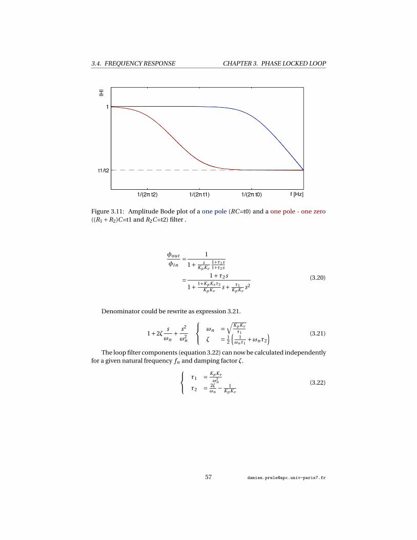
3.4. FREQUENCY RESPONSE CHAPTER 3. PHASE LOCKED LOOP
Figure 3.11: Amplitude Bode plot of a one pole (RC =t0) and a one pole - one zero((R1 +R2)C =t1 and R2C =t2) filter .
φout
φi n= 1
1+ sKp Kv
1+τ1s1+τ2s
= 1+τ2s
1+ 1+Kp Kvτ2
Kp Kvs + τ1
Kp Kvs2
(3.20)
Denominator could be rewrite as expression 3.21.
1+2ζs
ωn+ s2
ω2n
ωn =√
Kp Kv
τ1
ζ = 12
(1
ωnτ1+ωnτ2
) (3.21)
The loop filter components (equation 3.22) can now be calculated independentlyfor a given natural frequency fn and damping factor ζ. τ1 = Kp Kv
ω2n
τ2 = 2ζωn
− 1Kp Kv
(3.22)
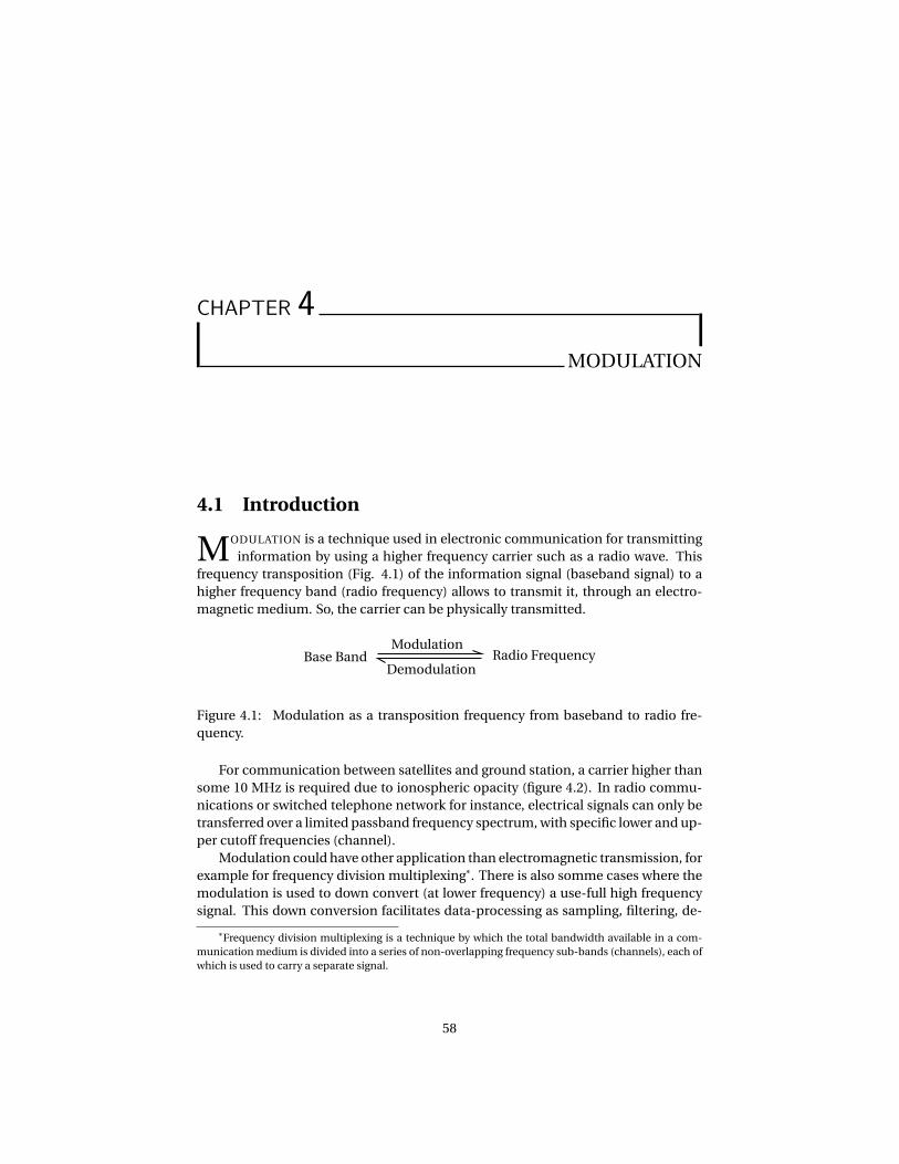
CHAPTER 4MODULATION
4.1 Introduction
MODULATION is a technique used in electronic communication for transmittinginformation by using a higher frequency carrier such as a radio wave. This
frequency transposition (Fig. 4.1) of the information signal (baseband signal) to ahigher frequency band (radio frequency) allows to transmit it, through an electro-magnetic medium. So, the carrier can be physically transmitted.
Base BandModulation
Radio FrequencyDemodulation
Figure 4.1: Modulation as a transposition frequency from baseband to radio fre-quency.
For communication between satellites and ground station, a carrier higher thansome 10 MHz is required due to ionospheric opacity (figure 4.2). In radio commu-nications or switched telephone network for instance, electrical signals can only betransferred over a limited passband frequency spectrum, with specific lower and up-per cutoff frequencies (channel).
Modulation could have other application than electromagnetic transmission, forexample for frequency division multiplexing*. There is also somme cases where themodulation is used to down convert (at lower frequency) a use-full high frequencysignal. This down conversion facilitates data-processing as sampling, filtering, de-
*Frequency division multiplexing is a technique by which the total bandwidth available in a com-munication medium is divided into a series of non-overlapping frequency sub-bands (channels), each ofwhich is used to carry a separate signal.
58
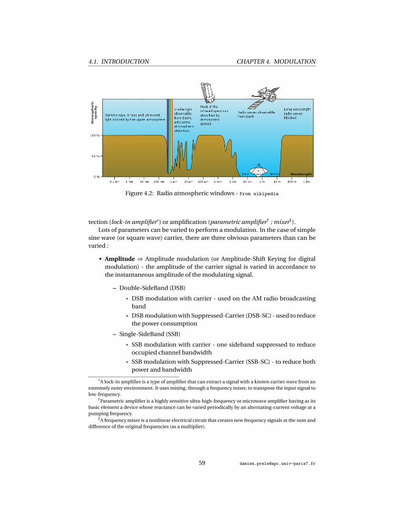
4.1. INTRODUCTION CHAPTER 4. MODULATION
Figure 4.2: Radio atmospheric windows - from wikipedia
tection (lock-in amplifier*) or amplification (parametric amplifier† ; mixer‡).Lots of parameters can be varied to perform a modulation. In the case of simple
sine wave (or square wave) carrier, there are three obvious parameters than can bevaried :
• Amplitude ⇒ Amplitude modulation (or Amplitude-Shift Keying for digitalmodulation) - the amplitude of the carrier signal is varied in accordance tothe instantaneous amplitude of the modulating signal.
– Double-SideBand (DSB)
* DSB modulation with carrier - used on the AM radio broadcastingband
* DSB modulation with Suppressed-Carrier (DSB-SC) - used to reducethe power consumption
– Single-SideBand (SSB)
* SSB modulation with carrier - one sideband suppressed to reduceoccupied channel bandwidth
* SSB modulation with Suppressed-Carrier (SSB-SC) - to reduce bothpower and bandwidth
*A lock-in amplifier is a type of amplifier that can extract a signal with a known carrier wave from anextremely noisy environment. It uses mixing, through a frequency mixer, to transpose the input signal tolow-frequency.
†Parametric amplifier is a highly sensitive ultra-high-frequency or microwave amplifier having as itsbasic element a device whose reactance can be varied periodically by an alternating-current voltage at apumping frequency.
‡A frequency mixer is a nonlinear electrical circuit that creates new frequency signals at the sum anddifference of the original frequencies (as a multiplier).

4.2. AMPLITUDE MODULATION CHAPTER 4. MODULATION
• Phase ⇒ Phase modulation (or Phase-Shift Keying) - the phase shift of thecarrier signal is varied in accordance to the instantaneous amplitude of themodulating signal.
• Frequency ⇒ Frequency modulation (or Frequency-Shift Keying) - the fre-quency of the carrier signal is varied in accordance to the instantaneous am-plitude of the modulating signal.
4.2 Amplitude modulation
A continuous wave radio-frequency signal (a sinusoidal carrier wave) has its ampli-tude modulated by the input waveform before transmission. Input waveform modi-fies the amplitude of the carrier wave and determines the envelope of the waveform.A simple form of amplitude modulation, often used for digital communications, ison-off keying*. This is used by radio amateurs to transmit Morse code.
Without transmission of the carrier, this modulation is obtained by simple mul-tiplication of an input signal by carrier signal. Figure 4.3 shows wave form and spec-trum of a multiplication of a sine wave input signal ( fs ) by a sine wave carrier ( f0).
Figure 4.3: Time waveform and spectrum of a double side band amplitude modula-tion without (SxC ) and with (SxC +C ) transmission of the carrier.
Indeed, multiplication transposes the input signal S at either side of the C carrierfrequency (frequency domain). Each sideband is equal in bandwidth to that of the
*a type of amplitude-shift keying in which binary data is represented by the presence or absence ofa carrier.
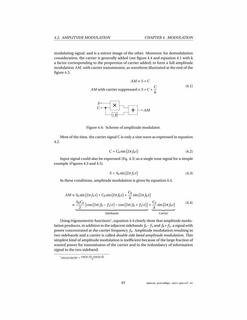
4.2. AMPLITUDE MODULATION CHAPTER 4. MODULATION
modulating signal, and is a mirror image of the other. Moreover, for demodulationconsideration, the carrier is generally added (see figure 4.4 and equation 4.1 with ka factor corresponding to the proportion of carrier added) to form a full amplitudemodulation AM , with carrier transmission, as waveform illustrated at the end of thefigure 4.3.
AM ≡ S ×C
AM with carrier suppressed ≡ S ×C + C
k
(4.1)
SC ×
÷k+ AM
Figure 4.4: Scheme of amplitude modulator.
Most of the time, the carrier signal C is only a sine wave as expressed in equation4.2.
C =C0 sin(2π f0t
)(4.2)
Input signal could also be expressed (Eq. 4.3) as a single tone signal for a simpleexample (Figures 4.3 and 4.5).
S = S0 sin(2π fS t
)(4.3)
In these conditions, amplitude modulation is given by equation 4.4.
AM ≡ S0 sin(2π fS t
)×C0 sin(2π f0t
)+ C0
ksin
(2π f0t
)≡ S0C0
2
[cos
(2π( f0 − fS )t
)−cos(2π( f0 + fS )t
)]︸ ︷︷ ︸
SideBands
+ C0
ksin
(2π f0t
)︸ ︷︷ ︸
Carrier
(4.4)
Using trigonometric functions*, equation 4.4 clearly show that amplitude modu-lation produces, in addition to the adjacent sidebands f0− fS and f0+ fS , a signal withpower concentrated at the carrier frequency f0. Amplitude modulation resulting intwo sidebands and a carrier is called double side band amplitude modulation. Thissimplest kind of amplitude modulation is inefficient because of the large fraction ofwasted power for transmission of the carrier and in the redundancy of informationsignal in the two sideband.
*sin(a)sin(b) = cos(a−b)−cos(a+b)2

4.2. AMPLITUDE MODULATION CHAPTER 4. MODULATION
Increasing the efficiency : The carrier and/or one sideband may be suppressed atthe expense of increased transmitter and receiver complexity. For reception, sup-pression of the carrier imply to restore it by the use of a local oscillator generatedby a phase locked loop for example. Whereas in the case of carrier transmission, asimple rectifier diode could be used for demodulation (detection).
Suppressing both the carrier and one of the sidebands also improves bandwidthefficiency. This is single-sideband modulation, widely used in amateur radio andother low consumption communication applications.
4.2.1 Modulation index
The modulation index (also called "modulation depth") quantify the evolution ofthe carrier signal around its unmodulated level. It is defined differently in eachmodulation scheme. In the case of amplitude modulation, modulation index m isthe ratio between the input signal amplitude S0 and the unmodulated transmittedcarrier amplitude C0
k (defined as expression 4.5).
m = kS0
C0(4.5)
So if carrier amplitude varies by 50% above and below its unmodulated level, themodulation index is equal to 0.5. k = m in the case of unity amplitude (C0 = S0 = 1).Figure 4.5 shows in time domain and frequency domain, the waveform of amplitudemodulation for different modulation index.
Figure 4.5: Different modulation index, from 50% (m = 0.5) to 200% (m = 2) andwithout carrier (m = ∞) in time domain and frequency domain.
On the spectrum representation, amplitude at each frequency can be easily ob-tained by using the equation 4.4. Techniques to graphically estimate the modulation
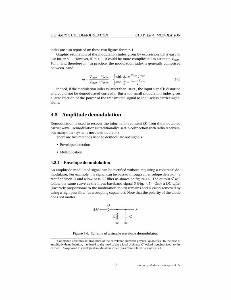
4.3. AMPLITUDE DEMODULATION CHAPTER 4. MODULATION
index are also reported on these two figures for m ≤ 1.Graphic estimation of the modulation index given by expression 4.6 is easy to
use for m ≤ 1. However, if m > 1, it could be more complicated to estimate Vmax ,Vmi n , and therefore m. In practice, the modulation index is generally comprisedbetween 0 and 1.
m = Vmax −Vmi n
Vmax +Vmi n
with S0 = Vmax−Vmi n
2
and C0k = Vmax+Vmi n
2
(4.6)
Indeed, if the modulation index is larger than 100 %, the input signal is distortedand could not be demodulated correctly. But a too small modulation index givesa large fraction of the power of the transmitted signal to the useless carrier signalalone.
4.3 Amplitude demodulation
Demodulation is used to recover the information content (S) from the modulatedcarrier wave. Demodulation is traditionally used in connection with radio receivers,but many other systems need demodulators.
There are two methods used to demodulate AM signals :
• Envelope detection
• Multiplication
4.3.1 Envelope demodulation
An amplitude modulated signal can be rectified without requiring a coherent* de-modulator. For example, the signal can be passed through an envelope detector : arectifier diode D and a low-pass RC filter as shown on figure 4.6. The output S′ willfollow the same curve as the input baseband signal S (Fig. 4.7). Only a DC offset(inversely proportional to the modulation index) remains and is easily removed byusing a high pass filter (as a coupling capacitor). Note that the polarity of the diodedoes not matter.
AMD
S′
R C
Figure 4.6: Scheme of a simple envelope demodulator.
*Coherence describes all properties of the correlation between physical quantities. In the case ofamplitude demodulation, it referred to the need of use a local oscillator C’ locked (synchronized) to thecarrier C. As opposed to envelope demodulation which doesn’t need local oscillator at all.

4.3. AMPLITUDE DEMODULATION CHAPTER 4. MODULATION
Rectifying can be modelized by an absolute value function : "||" and Low PassFiltering is noted "LPF ". So, envelope detection can be expressed as equation 4.7.
LPF
[∣∣∣∣S ×C + C
k
∣∣∣∣]= S′+ cst (4.7)
• The rectifier may be in the form of a single diode D, or anything that will passcurrent in one direction only*.
• The filter is usually a RC low-pass type when the difference in frequency be-tween the signal and the carrier is very large†. Furthermore, the filter functioncan sometimes be achieved by relying on the limited frequency response ofthe circuitry following the rectifier.
However, only amplitude modulation with a modulation index smaller than100% can be demodulated by envelope detection. Indeed, for a modulation indexlarger than 100%, or downright without carrier, envelope detection introduces nec-essarily large distortions. Figure 4.8 shows, for example, a rectifying detection of anamplitude modulation without carrier (S×C). In this extreme cases where m = ∞,the demodulated signal is roughly a sine waves, but at twice (!) the frequency of theinput signal.
+ To avoid this kind of distortions, a coherent demodulation is required.
4.3.2 Product demodulation
The product detector, illustrated by figure 4.9, multiplies the incoming modulatedsignal AM by the signal of a local oscillator C ′. C ′ need to have the same frequencyand phase as the carrier C of the incoming signal‡. After low pass filtering (LPF) andsuppression of the DC offset, the original signal will result as S′ given by expression4.8.
LPF
[(S ×C + C
k
)×C ′
]= S′+ cst (4.8)
Using the same example as for modulation equation 4.4 and for C ′ =C , a productdetection before the filtering could be expressed as equation 4.9. Using trigonomet-ric functions§, this expression shows that the information content S is restored inthe base-band fS , while the carrier and harmonics are pushed around 2 f0 and aretherefore easily filtered.
*Many natural substances exhibit rectifiyng behavior, which is why envelope demodulation was theearliest demodulation technique used in radio.
†In the case of AM radio broadcast, a carrier from few 100 kHz to few MHz is used for 10 kHz signalbandwidth (audio.). Regarding satellite communications, frequency carrier is of the order of several GHz;far away the signal bandwidth. For these kind of applications of the modulation, a simple first orderlow-pass filter is generally enough to attenuate residuals carrier harmonics.
‡If C ′ is in opposite-phase as compare to C, the demodulated signal is always = 0 !§sin(a)cos(b) = sin(a+b)+sin(a−b)
2 ; sin2(a) = 1−cos(2a)2 ; sin(−a) =−sin(a)

4.3. AMPLITUDE DEMODULATION CHAPTER 4. MODULATION
Figure 4.7: Waveform of an envelope detection : Signal S, Carrier C, AM with aunity modulation index S×C+C, Rectifying as an absolute value |S×C+C| and lowpass filtering LPF
(|S×C+C|
)for a complete reconstruction of the input signal S.
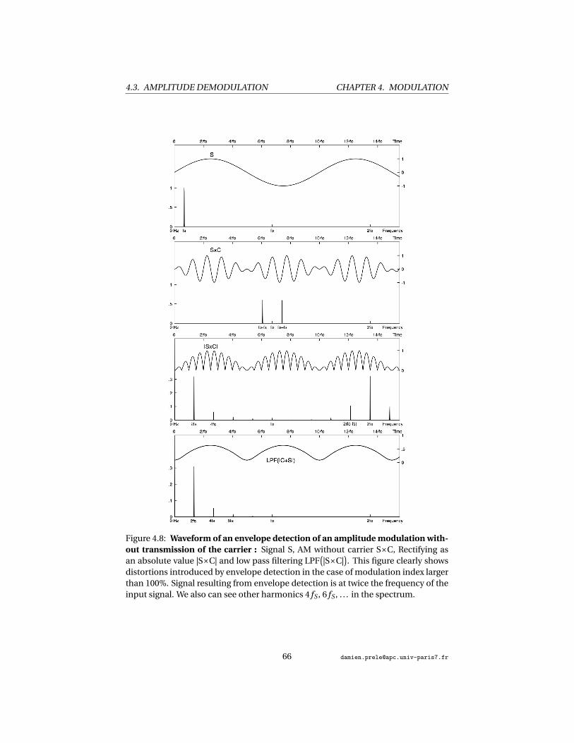
4.3. AMPLITUDE DEMODULATION CHAPTER 4. MODULATION
Figure 4.8: Waveform of an envelope detection of an amplitude modulation with-out transmission of the carrier : Signal S, AM without carrier S×C, Rectifying asan absolute value |S×C| and low pass filtering LPF
(|S×C|
). This figure clearly shows
distortions introduced by envelope detection in the case of modulation index largerthan 100%. Signal resulting from envelope detection is at twice the frequency of theinput signal. We also can see other harmonics 4 fS , 6 fS , . . . in the spectrum.
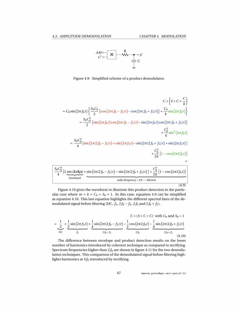
4.3. AMPLITUDE DEMODULATION CHAPTER 4. MODULATION
AMC ′ × R
S′
C
Figure 4.9: Simplified scheme of a product demodulator.
C ×(S ×C + C
k
)=C0 sin
(2π f0t
)S0C0
2
[cos
(2π( f0 − fS )t
)−cos(2π( f0 + fS )t
)]+ C0
ksin
(2π f0t
)= S0C 2
0
2
[sin
(2π f0t
)cos
(2π( f0 − fS )t
)−sin(2π f0t
)cos
(2π( f0 + fS )t
)]+C 2
0
ksin2 (
2π f0t)
= S0C 20
4
[sin
(2π(2 f0 − fS )t
)+ sin(2π fS t
)−sin(2π(2 f0 + fS )t
)+ sin(2π fS t
)]+C 2
0
2k
[1−cos
(2π2 f0t
)]=
S0C 20
4
[2 sin(2πfSt)︸ ︷︷ ︸
baseband
+sin(2π(2 f0 − fS )t
)− sin(2π(2 f0 + fS )t
)]+ C 20
2k
[1−cos
(2π2 f0t
)]︸ ︷︷ ︸
radio frequency + DC → filtered
(4.9)Figure 4.10 gives the waveform to illustrate this product detection in the partic-
ular case where m = k = C0 = S0 = 1. In this case, equation 4.9 can be simplifiedas equation 4.10. This last equation highlights the different spectral lines of the de-modulated signal before filtering (DC, fS , 2 f0 − fS , 2 f0 and 2 f0 + fS ).
C × (S ×C +C ) with C0 and S0 = 1
= 1
2︸︷︷︸DC
+ 1
2sin
(2π fS t
)︸ ︷︷ ︸
fS
+ 1
4sin
(2π(2 f0 − fS )t
)︸ ︷︷ ︸
2 f0− fS
− 1
2cos
(2π2 f0t
)︸ ︷︷ ︸
2 f0
− 1
4sin
(2π(2 f0 + fS )t
)︸ ︷︷ ︸
2 f0+ fS
(4.10)The difference between envelope and product detection results on the lower
number of harmonics introduced by coherent technique as compared to rectifying.Spectrum frequencies higher than 2 f0 are shown in figure 4.11 for the two demodu-lation techniques. This comparison of the demodulated signal before filtering high-lights harmonics at 4 f0 introduced by rectifying.

4.3. AMPLITUDE DEMODULATION CHAPTER 4. MODULATION
Figure 4.10: Waveform of a product detection : Signal S, Carrier C, AM signalS×C+C, demodulation C×(S×C+C) and low pass filtering LPF[C×(S×C+C)].
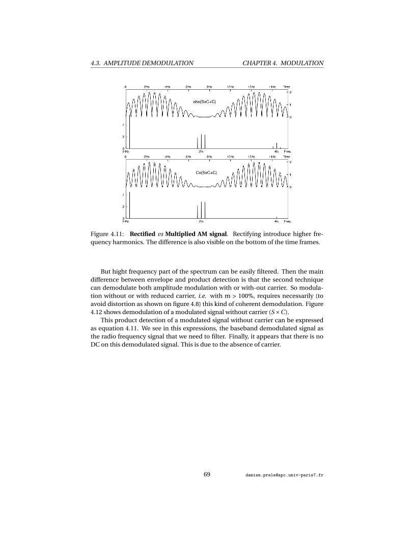
4.3. AMPLITUDE DEMODULATION CHAPTER 4. MODULATION
Figure 4.11: Rectified vs Multiplied AM signal. Rectifying introduce higher fre-quency harmonics. The difference is also visible on the bottom of the time frames.
But hight frequency part of the spectrum can be easily filtered. Then the maindifference between envelope and product detection is that the second techniquecan demodulate both amplitude modulation with or with-out carrier. So modula-tion without or with reduced carrier, i.e. with m > 100%, requires necessarily (toavoid distortion as shown on figure 4.8) this kind of coherent demodulation. Figure4.12 shows demodulation of a modulated signal without carrier (S ×C ).
This product detection of a modulated signal without carrier can be expressedas equation 4.11. We see in this expressions, the baseband demodulated signal asthe radio frequency signal that we need to filter. Finally, it appears that there is noDC on this demodulated signal. This is due to the absence of carrier.

4.3. AMPLITUDE DEMODULATION CHAPTER 4. MODULATION
Figure 4.12: Waveform of a product detection of an amplitude modulation with-out transmission of the carrier : Signal S, AM without carrier S×C, Demodulationby product S×S×C and low pass filtering LPF(S×S×C). With this product detection,there is no distortion, even if the carrier is not transmitted. Moreover, due to the factthat there is no carrier, there is no DC signal (offset) associated to the demodulatedsignal S′.

C ×S ×C
=C0 sin(2π f0t
) S0C0
2
[cos
(2π( f0 − fS )t
)−cos(2π( f0 + fS )t
)]
= S0C 20
2
[sin
(2π f0t
)cos
(2π( f0 − fS )t
)−sin(2π f0t
)cos
(2π( f0 + fS )t
)]
= S0C 20
4
[sin
(2π(2 f0 − fS )t
)+ sin(2π fS t
)−sin(2π(2 f0 + fS )t
)+ sin(2π fS t
)]=
S0C 20
4
[2sin(2πfSt)︸ ︷︷ ︸
baseband
+sin(2π(2 f0 − fS )t
)− sin(2π(2 f0 + fS )t
)]︸ ︷︷ ︸radio frequency - filtered
(4.11)
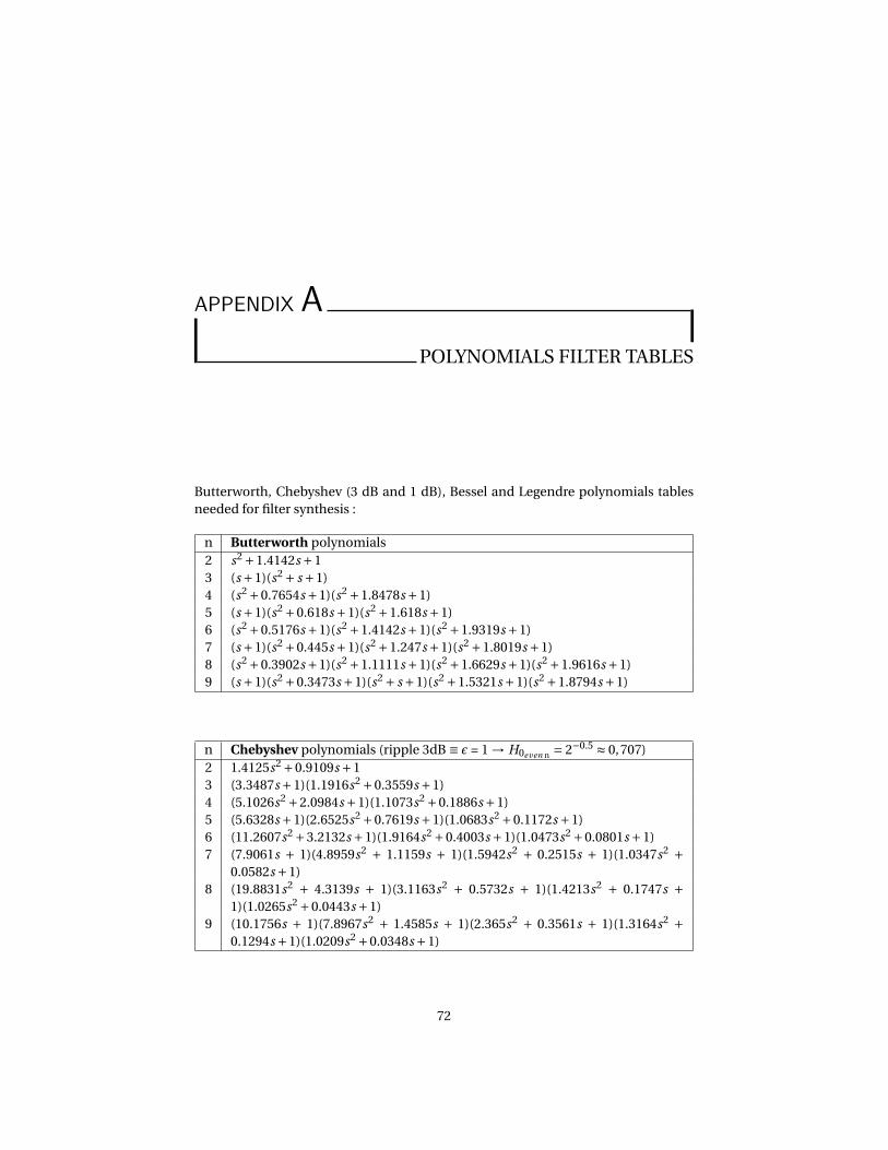
APPENDIX APOLYNOMIALS FILTER TABLES
Butterworth, Chebyshev (3 dB and 1 dB), Bessel and Legendre polynomials tablesneeded for filter synthesis :
n Butterworth polynomials2 s2 +1.4142s +13 (s +1)(s2 + s +1)4 (s2 +0.7654s +1)(s2 +1.8478s +1)5 (s +1)(s2 +0.618s +1)(s2 +1.618s +1)6 (s2 +0.5176s +1)(s2 +1.4142s +1)(s2 +1.9319s +1)7 (s +1)(s2 +0.445s +1)(s2 +1.247s +1)(s2 +1.8019s +1)8 (s2 +0.3902s +1)(s2 +1.1111s +1)(s2 +1.6629s +1)(s2 +1.9616s +1)9 (s +1)(s2 +0.3473s +1)(s2 + s +1)(s2 +1.5321s +1)(s2 +1.8794s +1)
n Chebyshev polynomials (ripple 3dB ≡ ε = 1 → H0even n = 2−0.5 ≈ 0,707)2 1.4125s2 +0.9109s +13 (3.3487s +1)(1.1916s2 +0.3559s +1)4 (5.1026s2 +2.0984s +1)(1.1073s2 +0.1886s +1)5 (5.6328s +1)(2.6525s2 +0.7619s +1)(1.0683s2 +0.1172s +1)6 (11.2607s2 +3.2132s +1)(1.9164s2 +0.4003s +1)(1.0473s2 +0.0801s +1)7 (7.9061s + 1)(4.8959s2 + 1.1159s + 1)(1.5942s2 + 0.2515s + 1)(1.0347s2 +
0.0582s +1)8 (19.8831s2 + 4.3139s + 1)(3.1163s2 + 0.5732s + 1)(1.4213s2 + 0.1747s +
1)(1.0265s2 +0.0443s +1)9 (10.1756s + 1)(7.8967s2 + 1.4585s + 1)(2.365s2 + 0.3561s + 1)(1.3164s2 +
0.1294s +1)(1.0209s2 +0.0348s +1)
72

n Chebyshev polynomials (ripple 1dB ≡ ε = 0.5 → H0even n = 1p1+0.52
≈ 0,894)
2 0.907s2 +0.9956s +13 (2.023s +1)(1.0058s2 +0.497s +1)4 (3.5791s2 +2.4113s +1)(1.0136s2 +0.2828s +1)5 (3.454s +1)(1.0118s2 +0.181s +1)(2.3293s2 +1.0911s +1)6 (1.793s2 +0.6092s +1)(1.0093s2 +0.1255s +1)(8.0188s2 +3.7217s +1)7 (4.868s+1)(1.0073s2+0.092s+1)(1.5303s2+0.3919s+1)(4.3393s2+1.6061s+1)8 (1.0058s2 + 0.0704s + 1)(2.9337s2 + 0.8754s + 1)(1.382s2 + 0.2755s +
1)(14.2326s2 +5.0098s +1)9 (6.276s+1)(1.2896s2+0.2054s+1)(1.0047s2+0.0556s+1)(2.2801s2+0.5566s+
1)(7.0242s2 +2.1033s +1)
n Bessel polynomials2 0.618s2 +1.3616s +13 (0.756s +1)(0.4771s2 +0.9996s +1)4 (0.4889s2 +1.3396s +1)(0.3889s2 +0.7742s +1)5 (0.665s +1)(0.3245s2 +0.6215s +1)(0.4128s2 +1.1401s +1)6 (0.2756s2 +0.513s +1)(0.3504s2 +0.9686s +1)(0.3887s2 +1.2217s +1)7 (0.593s+1)(0.238s2+0.4332s+1)(0.301s2+0.8303s+1)(0.3394s2+1.0944s+1)8 (0.2087s2 + 0.3727s + 1)(0.2621s2 + 0.7202s + 1)(0.2979s2 + 0.9753s +
1)(0.3161s2 +1.1112s +1)9 (0.538s+1)(0.231s2+0.6319s+1)(0.1854s2+0.3257s+1)(0.2635s2+0.8710s+
1)(0.2834s2 +1.0243s +1)
n Legendre polynomials2 s2 +1.4142s +13 (1.612s +1)(1.0744s2 +0.7417s +1)4 (1.0552s2 +0.4889s +1)(2.3213s2 +2.5522s +1)5 (2.136s +1)(1.0406s2 +0.3196s +1)(2.0115s2 +1.5614s +1)6 (1.7155s2 +1.06s +1)(1.0313s2 +0.2376s +1)(3.9963s2 +3.508s +1)7 (2.617s+1)(1.0241s2+0.1765s+1)(1.5102s2+0.7171s+1)(3.2679s2+2.2825s+
1)8 (1.3927s2 + 0.5411s + 1)(1.0195s2 + 0.1405s + 1)(5.9688s2 + 4.3832s +
1)(2.6116s2 +1.5684s +1)9 (3.07s+1)(1.3043s2+0.4103s+1)(2.1574s2+1.0724s+1)(1.0158s2+0.1119s+
1)(4.7851s2 +2.9606s +1)

74

APPENDIX BCD4046 DATA SHEET
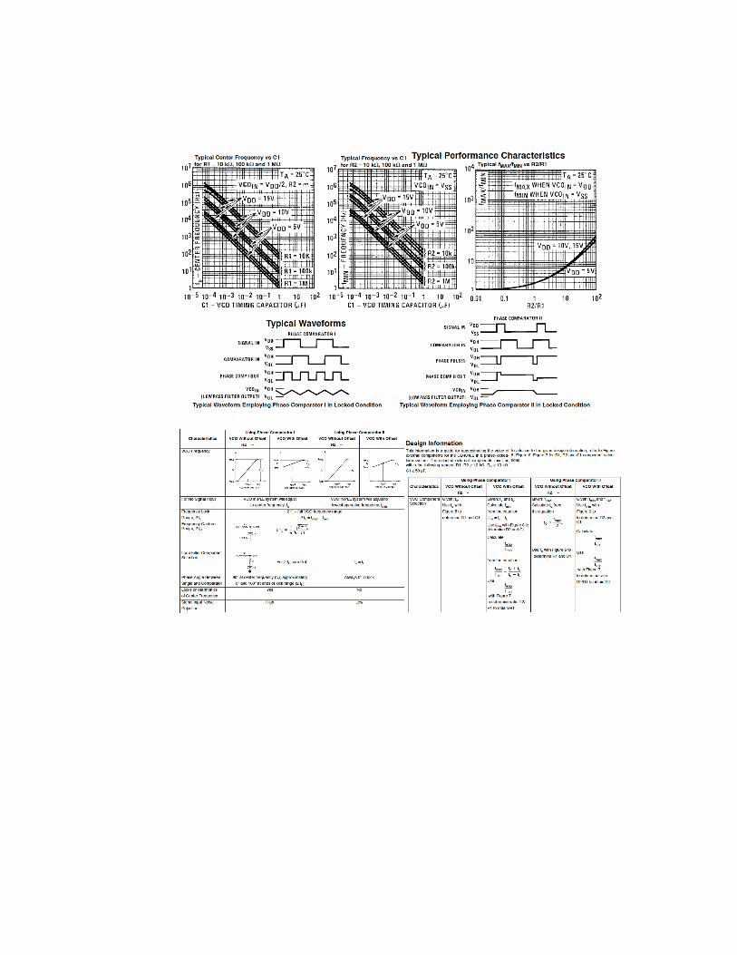

Notes
LIST OF FIGURES
1.1 Transfer function of ideal filter : Fixed gain in the pass band and zerogain everywhere else ; transition at the cutoff frequency. . . . . . . . . . 5
1.2 Passive low-pass filter : first order R-C, first order L-R and second orderL-C. . . . . . . . . . . . . . . . . . . . . . . . . . . . . . . . . . . . . . . . . 6
1.3 Impedance bridge voltage divider. . . . . . . . . . . . . . . . . . . . . . . 61.4 Passive band-pass LCR filter. . . . . . . . . . . . . . . . . . . . . . . . . . 81.5 Pole (6) and zero (l) representation of the RLC filter (Fig. 1.4) into the
s plane. . . . . . . . . . . . . . . . . . . . . . . . . . . . . . . . . . . . . . . 91.6 Stable if all poles are in the left hand s plane (i.e. have negative real
parts). . . . . . . . . . . . . . . . . . . . . . . . . . . . . . . . . . . . . . . . 91.7 Bode plot of the LCR band-pass filter figure 1.4. . . . . . . . . . . . . . . 101.8 Bode plot of a band-pass filter - Q = 0.01 ; 0.1 ; 0.25 ; 0.5 ; 1 ; 2 ; 4 ; 10 ;
100 (i.e. ζ = 50 ; 5 ; 2 ; 1 ; 0.5 ; 0.25 ; 0.125 ; 0.05 ; 0.005). . . . . . . . . . . 111.9 Cascading filter stages for higher-order filters. . . . . . . . . . . . . . . . 121.10 Pole locations of 1st , 2nd , 3r d , 4th and 5th order Butterworth filter. . . . 141.11 Bode plot of a second order Butterworth low pass filter. . . . . . . . . . 221.12 H0 the low frequency gain of a low-pass filter and H∞ the high fre-
quency gain of a high-pass filter. . . . . . . . . . . . . . . . . . . . . . . . 221.13 Sallen-Key generic topology. . . . . . . . . . . . . . . . . . . . . . . . . . 241.14 Sallen-Key low-pass filter. . . . . . . . . . . . . . . . . . . . . . . . . . . . 241.15 Sallen-Key high-pass filter. . . . . . . . . . . . . . . . . . . . . . . . . . . 251.16 Cascading low and high pass filter for band-pass filtering. . . . . . . . . 251.17 Sallen-Key band-pass filter. . . . . . . . . . . . . . . . . . . . . . . . . . . 261.18 Voltage-controlled voltage-source (VCVS) filter topology band-pass fil-
ter. . . . . . . . . . . . . . . . . . . . . . . . . . . . . . . . . . . . . . . . . . 261.19 Paralleling low and high pass filter for band-pass filtering. . . . . . . . . 271.20 Sallen-Key band-reject filter. . . . . . . . . . . . . . . . . . . . . . . . . . 271.21 Filter amplitude response limits. . . . . . . . . . . . . . . . . . . . . . . . 281.22 Steepness and phase linearity filter comparison. . . . . . . . . . . . . . 29
78
1.23 Frequency response of a Butterworth, Chebyshev, Bessel and Legen-dre 5th order low pass filter around cutoff frequency and far after it.Dashed line represent a f −5 slope for comparison to 5th order filterrolloff. . . . . . . . . . . . . . . . . . . . . . . . . . . . . . . . . . . . . . . . 31
1.24 Normalized ( f0 = 1) time response (step) of multipole (2 to 10) Butter-worth, Chebyshev 1dB and Bessel filters. . . . . . . . . . . . . . . . . . . 31
1.25 Frequency response of a Butterworth low pass filter for n = 2 to 5. . . . 321.26 Frequency response of a Chebishev (ε= 1) low pass filter for n = 2 to 5. 331.27 Zoom in the passband of the frequency response of a Chebishev (ε= 1)
low pass filter for n = 4 and 5. . . . . . . . . . . . . . . . . . . . . . . . . . 331.28 Frequency response of a Chebishev (ε= 0.5) low pass filter for n = 2 to
5 order filter rolloff. . . . . . . . . . . . . . . . . . . . . . . . . . . . . . . . 341.29 Zoom in the passband of the frequency response of a Chebishev (ε =
0.5) low pass filter for n = 2 to 5. . . . . . . . . . . . . . . . . . . . . . . . . 341.30 Comparison between frequency response of two Chebishev low pass
filters of 5th order, one with a ripple factor of 1 dB, and the other with3 dB. . . . . . . . . . . . . . . . . . . . . . . . . . . . . . . . . . . . . . . . . 35
1.31 Frequency response of a Bessel low pass filter for n = 2 to 5. . . . . . . . 36
1.32 Comparison of the delay time as a function of frequency ( ffc
) betweena Bessel, a Butterworth and a Chebyshev low-pass filter (n=4). . . . . . 36
1.33 Frequency response of a Legendre low pass filter for n = 2 to 5 . . . . . 361.34 Zoom on the passband of the frequency response of a Legendre low
pass filter for n = 2 to 5. . . . . . . . . . . . . . . . . . . . . . . . . . . . . . 371.35 Equivalence between Resistor and Switched Capacitor. . . . . . . . . . 371.36 Equivalence between RC filter and switched capacitor filter. . . . . . . . 37
2.1 DC/DC converter for space applications - CLYDE SPACE . . . . . . . . . . 392.2 Buck topology of a step-down DC/DC converter. . . . . . . . . . . . . . 402.3 Simplified Buck converter circuit for the two configurations : left when
the transistor T conducts (ON); right when it is OFF. . . . . . . . . . . . 402.4 Voltages and current as a function of time for an ideal buck converter
operating in continuous mode. . . . . . . . . . . . . . . . . . . . . . . . . 422.5 Boost topology of a step-up DC/DC converter. . . . . . . . . . . . . . . . 422.6 Buck-boost Inverting topology of DC/DC converter. Vout is of the op-
posite polarity as Vi n . . . . . . . . . . . . . . . . . . . . . . . . . . . . . . . 432.7 Flyback topology of an isolated DC/DC converter. . . . . . . . . . . . . . 442.8 Principle of a DC/DC converter feedback voltage regulation. D is the
duty cycle of the switching transistor. . . . . . . . . . . . . . . . . . . . . 452.9 Voltage regulation of a Buck DC/DC converter by using Pulse Width
Modulation (PWM). . . . . . . . . . . . . . . . . . . . . . . . . . . . . . . . 452.10 Pulse Width Modulation (PWM). . . . . . . . . . . . . . . . . . . . . . . . 46
3.1 PLLs used for space applications (Peregrine Semiconductor); GPS constel-lation around the Earth. . . . . . . . . . . . . . . . . . . . . . . . . . . . . 47
3.2 Block diagram of a PLL. . . . . . . . . . . . . . . . . . . . . . . . . . . . . 483.3 XOR phase comparator. . . . . . . . . . . . . . . . . . . . . . . . . . . . . 50
3.4 Periodic characteristic of an XOR phase comparator and a typical op-erating point. The slope Kp is the gain of the comparator. . . . . . . . . 51
3.5 VCO characteristic : VV CO as a function of fV CO . . . . . . . . . . . . . . . 523.6 Scope of the 2 main frequency ranges of a PLL : Lock (or Hold) range
and Capture range (more or less defines due to pull-in effect). . . . . . 533.7 Hysteretic PLL characteristic. . . . . . . . . . . . . . . . . . . . . . . . . . 543.8 Block diagram of PLL on phase domain. . . . . . . . . . . . . . . . . . . 553.9 One pole filter used as PLL loop filter. . . . . . . . . . . . . . . . . . . . . 553.10 One pole - one zero filter used as PLL loop filter. . . . . . . . . . . . . . . 563.11 Amplitude Bode plot of a one pole (RC =t0) and a one pole - one zero
((R1 +R2)C =t1 and R2C =t2) filter . . . . . . . . . . . . . . . . . . . . . . . 57
4.1 Modulation as a transposition frequency from baseband to radio fre-quency. . . . . . . . . . . . . . . . . . . . . . . . . . . . . . . . . . . . . . . 58
4.2 Radio atmospheric windows - from wikipedia . . . . . . . . . . . . . . . . 594.3 Time waveform and spectrum of a double side band amplitude mod-
ulation without (SxC ) and with (SxC +C ) transmission of the carrier. . . 604.4 Scheme of amplitude modulator. . . . . . . . . . . . . . . . . . . . . . . . 614.5 Different modulation index, from 50% (m = 0.5) to 200% (m = 2) and
without carrier (m = ∞) in time domain and frequency domain. . . . . 624.6 Scheme of a simple envelope demodulator. . . . . . . . . . . . . . . . . 634.7 Waveform of an envelope detection : Signal S, Carrier C, AM with a
unity modulation index S×C+C, Rectifying as an absolute value |S×C+C|and low pass filtering LPF
(|S×C+C|
)for a complete reconstruction of
the input signal S. . . . . . . . . . . . . . . . . . . . . . . . . . . . . . . . . 654.8 Waveform of an envelope detection of an amplitude modulation with-
out transmission of the carrier : Signal S, AM without carrier S×C,Rectifying as an absolute value |S×C| and low pass filtering LPF
(|S×C|
).
This figure clearly shows distortions introduced by envelope detectionin the case of modulation index larger than 100%. Signal resulting fromenvelope detection is at twice the frequency of the input signal. Wealso can see other harmonics 4 fS , 6 fS , . . . in the spectrum. . . . . . . . . 66
4.9 Simplified scheme of a product demodulator. . . . . . . . . . . . . . . . 674.10 Waveform of a product detection : Signal S, Carrier C, AM signal S×C+C,
demodulation C×(S×C+C) and low pass filtering LPF[C×(S×C+C)]. . . 684.11 Rectified vs Multiplied AM signal. Rectifying introduce higher fre-
quency harmonics. The difference is also visible on the bottom of thetime frames. . . . . . . . . . . . . . . . . . . . . . . . . . . . . . . . . . . . 69
4.12 Waveform of a product detection of an amplitude modulation with-out transmission of the carrier : Signal S, AM without carrier S×C,Demodulation by product S×S×C and low pass filtering LPF(S×S×C).With this product detection, there is no distortion, even if the carrieris not transmitted. Moreover, due to the fact that there is no carrier,there is no DC signal (offset) associated to the demodulated signal S′. . 70
LIST OF TABLES
1.1 Bessel conversion factor . . . . . . . . . . . . . . . . . . . . . . . . . . . . 161.2 Butterworth polynomials complex roots. . . . . . . . . . . . . . . . . . . 19
1.3 Butterworth polynomials coefficients cx . Pn = Bn =n∑
x=0cx sx = cn sn +
cn−1sn−1 +·· ·+c1s + c0. . . . . . . . . . . . . . . . . . . . . . . . . . . . . 201.4 Butterworth polynomials quadratic factors. . . . . . . . . . . . . . . . . 201.5 Butterworth normalized cutoff frequency (Scaling Factor - SF) and qual-
ity factor (Q) for each stages. . . . . . . . . . . . . . . . . . . . . . . . . . 211.6 Filter normalized transposition. . . . . . . . . . . . . . . . . . . . . . . . 231.7 Butterworth, Chebyshev, Bessel and Legendre filter advantages/disadvantages. 291.8 Butterworth, Chebyshev, Bessel and Legendre filter comparison. . . . . 30
3.1 XOR truth table. . . . . . . . . . . . . . . . . . . . . . . . . . . . . . . . . . 49
81