daniel minzari et al. manuscript submitted to eurocorr 7-11
TRANSCRIPT

Daniel Minzari et al. Manuscript submitted to Eurocorr 7-11 September 2008,
Edinburgh, UK
Electrolytic migration on electronic chip resistors in chloride environments
Daniel Minzari*, Morten S. Jellesen, Per Møller, Rajan Ambat
Department of Mechanical Engineering, Technical University of Denmark, DK 2800 Kgs. Lyngby, Denmark
Abstract A novel experimental setup has been developed, allowing ElectroChemical Migration (ECM) experiments to be conducted on single chip electronic components such as capacitors and resistors. Such technique could provide a methodology for assessment of the quality of electronic components prior to mounting them on to the PCB. In this work, the Single Component ElectroChemical Migration (SCECM) setup is used to investigate the effect of chloride concentration on the electrochemical migration of 97Sn3Pb solder terminals on a 10kΩ ceramic chip resistor size 0805. The material makeup of the chip resistor is investigated by SEM/EDS. Chloride concentrations investigated was 0, 10, 100 and 1000 ppm. Results from SCECM experiments suggest that the dissolution rate of Sn plays a significant role in the formation of dendrites and on the resistance of these. 1. Introduction Corrosion of electronics devices in humid environment is of serious concern today due to the combination of multimaterial use, potential bias and miniaturization on Printed Circuit Boards (PCB). Process and service related contaminations accelerate corrosion by making the environment more aggressive [1,2]. Due to corrosion problems life span of the product is reduced, and failure or loss of functionality of the device leads to severe economic loss, plant down time and customer dissatisfaction [3]. Miniaturization at all levels is one of the key factors reducing corrosion reliability. Over the last 10 years, size of the electronics has been reduced by over 70%. For flip chip ICs, miniaturization amounts to ~ 90%. The closer spacing increases the electric field (E = V/d), which makes corrosion cell formation easy during local condensation under humid environments. Under humid conditions a nano scale water layer is formed locally on the PCB components giving rise to a conducting path for current flow and thereby establishment of electrochemical cell between two points on PCBs. The potential bias on the PCB at adjacent points or dissimilar material combinations serves as thermodynamic driving force for the corrosion cell. Figure 1 shows two possibilities for the corrosion cell formation on the surface of the PCBs due to multimaterial combinations and potential bias. Process and service related contamination makes it easy to form the water layer as they are good water absorbers, while they also serve as a source for ions for electrical conductivity.
* Corresponding author: Email: [email protected] Fax: +45 4593 6213 (D. Minzari)

Figure 1: Two possibilities for corrosion cell formation on a PCB with condensed electrolyte: (a) Galvanic coupling due to different materials on PCB and (b) Formation of electrochemical cell between similar electrodes due to applied bias.
Electrochemical migration is a typical form of corrosion found on electronic systems [3-4]. In an electronic system, ECM occurs due to the presence of a potential gradient between two conductors connected by a thin layer of solution. For example two terminals of a chip capacitor or resistor on a PCB could act as anode and cathode if they are connected by a water layer. In this case, dissolved metal ions from the positive electrode (anode) migrate towards oppositely charged negative electrode (cathode) to deposit there. Process is similar to metal plating except for the growth of the deposit in the form of dendrites due to higher electric field acting between the deposited points and anode. Number and size of dendrites depends on the conductivity of the medium, with higher conductivity makes the electric field more uniform over the electrode surface. Growth of dendrites finally leads to electric short between two points on the PCB, which cause component failure or malfunction. However, not all metals on the PCB can cause electrolytic migration. Whether a specific metal ion can form dendrite or not depends on the stability of that ion in aqueous solution and of the over voltage required for deposition compared to hydrogen over voltage. Therefore, metals like Cu, Ag, Sn, Pb etc. on PCB are susceptible to electrolytic migration at least over a range of potentials and pH predicted by the Pourbaix diagram [5] where particular ions are stable. Two key factors increasing the electrolytic migration problem today is the miniaturization and contamination on the PCB surface. Miniaturization increases the electric field between two adjacent points on a PCB, while contamination provides increased conductivity for the water layer. At constant voltage, the electric field between the conductors rises inversely with the conductor spacing, and electrochemical migration is known to be enhanced under high electric fields [6-7]. ECM has traditionally been roughly divided into two sub-categories: humid ECM where a thin invisible moisture film is adsorbed to the surface and wet ECM where a visible layer of condensed water is present [8]. Silver and to some extent copper has been reported to migrate under humid conditions [9-14], while other susceptible metals usually require a visible water layer [8,15-25]. However, as distances on the PCB are getting smaller due to miniaturization, the risk of having a condensation nucleus expanding over two conductors increase, and the relevance for ECM under wet (condensed) conditions is therefore increasing.
2

The exact mechanism of electrolytic migration and influencing factors on a PCB surface vary from one application to another, and many factors are still unknown. Contaminations such as chloride ions play significant effect on migration, while pH of the solution layer determines the stability of the dissolved metal ions in the water layer for migration to occur [5]. Localized pH changes also occur during migration due to high voltages at the electrode and resulting faradic reactions. Sn and Pb are common metals on the PCB that are susceptible to electrolytic migration [1]. Tin and lead exists in the form of solder alloy on the PCB surface and also as outer layer of electrodes of components for example chip resistors and capacitors. Migration of these metals on PCB surface leads malfunction and failures of PCBs during service. A problem encountered when investigating ECM phenomenon directly on the PCB is the amount of parameters influencing the system, such as solder process, solder flux and heating profile to name a few. Such factors make reliable reproduction of experiments extremely difficult, thereby complicating interpretation and comparison of experimental results. In this paper, electrolytic migration on ceramic chip resistors has been investigated in detail using a Single Component ElectroChemical Migration (SCECM) setup attached with video microscope. In the SCECM setup, a single chip component can be loaded with applied potential on both sides to be exposed to micro-volumes environment, thus simulating a condensed corrosion environment. The resulting migration current can be monitored together with time lapse videoing of the migration phenomena. A great advantage of this experimental setup is that the components can be investigated in the as received condition, without any soldering process. Basic electrochemical behaviour of the chip resistor electrode materials was investigated using micro-electrochemical sep up with tip resolution of 0.4 mm. Material make up, microstructure, and corrosion morphology are investigated using Scanning Electron Microscope (SEM), EDS and optical microscopy. 2. Materials and Methods: 2.1. Electronic Components The electronic component used for investigation in this work is a commercially available 10kΩ Ceramic Chip Resistor (CCR) size 0805 (Figure 2). The dimensions of the chip resistor are: 2.0x1.2x0.45 mm. The component chosen for this investigation is a representative of the large number of chip resistors used for the electronic PCB production.
Figure 2: CCR size 0805 used in this work: (left) bottom side and (right) top side. Resistance of component is 10 kΩ.
3
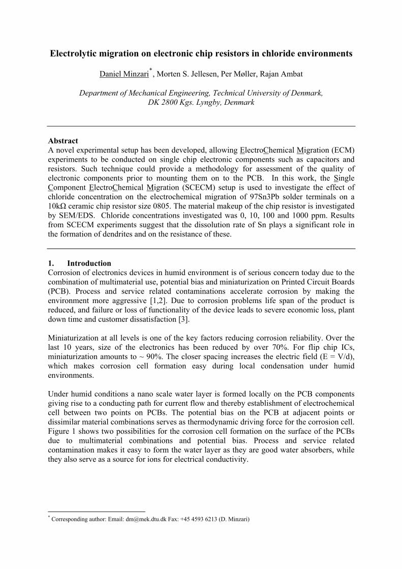
2.2. SCECM system: The SCECM set up consists of a glass chamber where opposite sides are fitted with two tiny adjustable probes, which acts as connections to each end of the components, in this case chip resistor (see Figure 3). One of the probes is fixed, while the other can be controlled in the transverse direction with micrometer precision. The probes are covered with silicone rubber, which is penetrated by the probe when a load is applied, thereby allowing electrical contact while at the same time providing corrosion protection to the probes.
Figure 3: (a) Schematic of the ECECM setup: 1. Specimen for investigation, 2. Droplet of solution, 3. Probes covered by silicone for insulation, 4. Experiment chamber, 5. Potentiostat, and 6. Video microscope. (b) Image of actual setup.
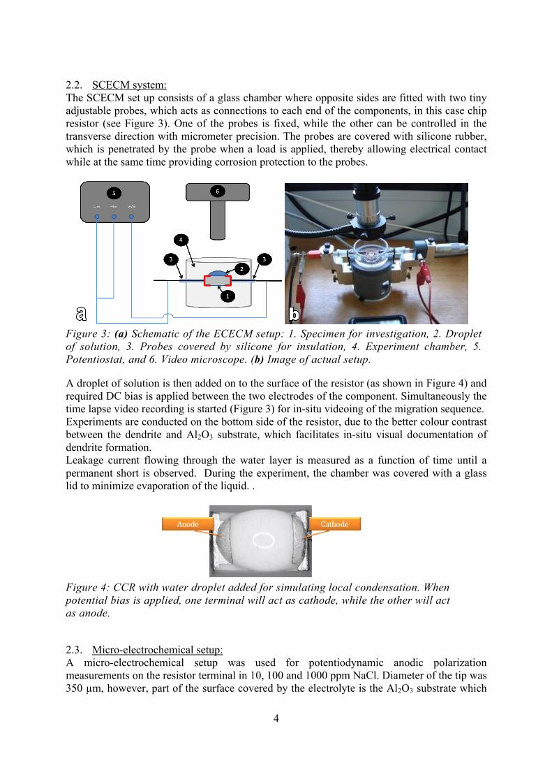
A droplet of solution is then added on to the surface of the resistor (as shown in Figure 4) and required DC bias is applied between the two electrodes of the component. Simultaneously the time lapse video recording is started (Figure 3) for in-situ videoing of the migration sequence. Experiments are conducted on the bottom side of the resistor, due to the better colour contrast between the dendrite and Al2O3 substrate, which facilitates in-situ visual documentation of dendrite formation. Leakage current flowing through the water layer is measured as a function of time until a permanent short is observed. During the experiment, the chamber was covered with a glass lid to minimize evaporation of the liquid. .
Figure 4: CCR with water droplet added for simulating local condensation. When potential bias is applied, one terminal will act as cathode, while the other will act as anode.
2.3. Micro-electrochemical setup: A micro-electrochemical setup was used for potentiodynamic anodic polarization measurements on the resistor terminal in 10, 100 and 1000 ppm NaCl. Diameter of the tip was 350 µm, however, part of the surface covered by the electrolyte is the Al2O3 substrate which
4

is inactive in the electrochemical measurements. By image analysis of corroded specimens, an electrode area of 0.003 cm2 was found.
Figure 5: Micro-electrochemical setup used in combination with the SCECM holder: 1. Specimen to be investigated, 2. Tip containing electrolyte, 3. Connection for counter electrode and 4. Connection for reference electrode.
2.4. Specimen preparation For SCECM measurements, chip resistors were handled by polymer tweezers and gloves to avoid any mechanical damage during handling. The potentiostat used for the SCECM experiments was a Gill AC potentiostat from ACM instruments. For 12V experiments, a current divider was used for increasing the potential output of the potentiostat. Microelectrochemical experiments were conducted using a CH Instruments 600 B electrochemical analyzer and an Ag/AgCl reference electrode (3M NaCl giving a potential of 215 mV vs. SHE). Open Circuit Potential (OCP) was held for 300 s after which anodic polarization was conducted from OCP -20mV to 2000mV with a scan rate of 1 mV/s. Electrolyte in the micro-electrochemical tip was purged between each experiment. Sodium chloride solutions with concentrations of 0, 10, 100, and 1000 ppm in DI water were used for the experiments. All the solutions were prepared using A.R grade NaCl in de-ionized water. All experiments were carried out in the aerated conditions. . 2.5. SEM/EDS and FEG-SEM Analysis Microstructural characterisation of the components before and after SCECM experiments were done using Scanning Electron Microscopy (SEM - JEOL 5900) and chemical analysis was carried out using Energy Dispersive x-ray Spectroscopy (EDS - Oxford Link ISIS) analyser attached to the SEM. Field Emission Gun Scanning Electron Microscopy (FEG-SEM) was performed using a Zeiss 1540EsB cross beam for high resolution images of surface topography of solder terminals.
3. Results 3.1. Material make up and microstructure of chip resistor The CCR (Figure 2) is a surface mount component that consists of a sintered ceramic body, on top of which a resistive layer is placed. An inert glass coating is applied in order to protect
5

the resistive layer and connections to the resistive layer are made by adding metal terminals at both ends of the component. A schematic of the material makeup is presented on Figure 6.
Figure 6: Schematic of general material make-up of a surface mount chip resistor.
Figure 7 (a) shows the magnified view of the surface of the electrodes. Top surface of the electrodes are made of Sn3Pb alloy. Surface morphology of the electrode shows that the surface is non-uniform and with very rough areas indicative of a barrel plating technique used for manufacturing of the outer layer of these resistors.
Figure 7: (a) FEG-SEM picture of terminal surface (Sn layer) and (b): SEM cross section of part of terminal
Figure 7 (b) shows the cross section of the resistor and different layers of electrode materials and resistive element. Following is the summary of detailed EDS analysis. The resistive layer was found to contain oxides of Pb and Si with smaller amounts of Ca, Ti, Cr, Zn and Ag. This layer is covered by a silicon oxide glass layer. Ag layers are used to connect the resistive layer to the terminals that consist of a Sn3Pb outer layer on top of Ni layer, which is on top of Ag layers. The ceramic body is made of aluminium oxide, with small amount of silicon oxide. 3.2. Anodic Polarization of component terminals Overlay of the anodic polarization curves for the solder terminal in increasing Cl- concentrations is shown in Figure 8. The dissolution rate of the tin is seen to increase with the chloride concentration. Almost a decade increase in current was observed with 10 times increase in chloride concentration. At high potentials, polarization curves flatten as the ohmic limit of the solution is reached and little increase in current density is seen with increase in potential.
6

Figure 8: Potentiodynamic anodic polarisation curves for solder terminals on ceramic chip resistor.
1000 ppm NaCl
100 ppm NaCl
10 ppm NaCl
Corroded area after 1000 ppm NaCl anodic polarization experiment was investigated using SEM showing selective dissolution of tin exposing nickel layer beneath as seen in Figure 9. Islands containing higher amount of tin and oxygen was observed, probably corrosion products.
Figure 9: High magnification SEM image (SEI Mode) of corroded area from anodic polarization at low (a) and high (b) magnifications
3.3. Electrolytic migration experiments in chloride solutions Effect of chloride ion concentration on electrolytic migration was studied using SCECM setup. Figure 10 shows an illustrative experiment, where a droplet of 10 ppm NaCl was added under 3V bias. First visible dendrite nucleation was observed after approx. 7 min 30 sec. At this stage, a little corrosion is observed at the anode and some precipitates, most likely tin hydroxides are seen to be present in the solution. After first visible nucleation of a dendrite was observed, a period of approximately 2 min dendrite growth occurred until the dendrite finally reached the anode short circuiting the component.
7

The current-time curve for the experiment is shown in Figure 10 along with images of dendrite at the time of first short (image 1), branching and agglomeration of dendrites (images 2+3) and at the end of the experiment where the solution has dried out (image 4).
300
320
340
360
380
400
420
0 8 16 24 32 40
Cur
rent
(µA
)
Time (min)
Figure 10: Current-time curve for dendrite formation in 10 ppm NaCl under 3V bias until electrolyte has evaporated, along selected images of dendrites. For all images, cathode is on the right and anode is on the left. The times of image acquisition are marked by dotted lines on the current-time curve.
432 1
1 2 3 4
Shorting due to dendrite is seen to increase the current to a level of 400 µA, until the dendrite bridge burns off at approx t=20 min. and current drops back to base level of 300 µA. After 33 min a new dendrite bridge is formed which is again burns off, and this behaviour continues until the electrolyte is completely evaporated from the component. Figure 11 shows specimens after SCECM experiments at 3V and 12V respectively at chloride concentrations of 0 and 1000 ppm. Images were acquired at the time where the dendrite first reaches the anode. For experiments where no migration was observed, the image presented is taken after the experiment has finished and the electrolyte has dried out.
8

Figure 11: Dendrite and corrosion morphology for 3V (top) and 12V (below) experiments for chloride concentrations of 0 and 1000 ppm. For all images, cathode is on right and anode is on left.
9
For 12 V experiments using 100 (not shown here) and 1000 ppm NaCl, a grey/turquoise corrosion product is seen (see Figure 11). EDS analysis showed the presence of both Ni, Sn and O, indicating that the corrosion product is a mixture of hydroxides of these. However, Ni was not detected in the dendrites. Migration current vs. time curves for representative experiments at 3V and 12V bias are presented in Figure 12. It is noted, that the current through the electrolyte is very small compared to that passing through the dendrite bridge. It is also noted, that the current through the dendrites that are formed at 12V bias is significantly higher than that of 3V.
3V 0ppm 3V 1000ppm
12V 0ppm 12V 1000ppm

Figure 12: Current time curves for: (a) 3V and (b) 12V at varying chloride concentrations
4. Discussion In agreement with field failures reported on electronic migration on PCBs, chip resistors tested in this investigation was found to be susceptible to electrolytic migration due to the presence of susceptible electrode materials. Some scatter in behaviour was observed between similar components with some of them showing dendrite formation, while others not with similar test parameters. Therefore, experiments in each case were repeated several times and the results reported in this paper represent typical behaviours observed. At higher potentials it seems that the dendrites are thinner compared to that at lower potentials. This behaviour is believed to be due to effects such as higher electric field, tin ion concentration, conductivity of the solution, and stability of metal ions. Increased chloride concentration increase the dissolution of the metal ions with concentrations in the solution
10

layer above the stability limit leading to precipitation of hydroxides. Such hydroxide particles could be incorporated into the dendrites. In general, the probability of experiencing a short was found to increase initially with change in chloride concentration from 0 to 10 ppm at 3V, but further increase in concentration reduced the probability for short. Similar behaviour was observed at 12V except for the shift in the change over chloride concentration to 100 ppm. Further investigation is needed to find the exact reason for this behaviour, but it is appears to be due to change in local pH resulting from increased faradaic reactions and correspondingly the change stability of the metal ions. As expected time to first short was found to be longer at lower potentials (3V) compared to that at 12 V bias. Also, the droplet used for 3V experiments had less tendency to evaporate, indicating less generation of heat in the component during the experiment. Both aspects correlate with use of higher voltage that results in higher current through the resistor to heat up and higher voltage also increases the migration kinetics. As dendrite is formed on the surface of the component, the system can be represented by an equivalent circuit, consisting of a parallel series of a resistance from the resistive layer of the component and the resistance through the dendrite. A sketch of a simplified system is represented in Figure 13.
Dendrite
11
Figure 13: Simple equivalent circuit for the resistor-electrolyte-dendrite system
As the resistance through the electrolyte is very high, compared to the resistances through the resistor and dendrite, this can be neglected and the resistance through the dendrite can then be roughly estimated using simple Ohms law calculation of the dendrite-resistor system.
As a measure of the conductivity of the dendrites, the maximal current measured in experiments, where dendrite formation was observed, has been used to estimate the dendrite resistance. Figure 14 shows the dendrite resistance as a function of the chloride concentration. Values are only taken from experiments where dendrite formation was observed and averaged. Therefore, it should be noted that the values presented are not exact and should only be regarded as estimates.
Resistor
Electrolyte

Figure 14: Dendrite resistance at varying chloride concentrations for 3V and 12V experiments.
It is interesting to note that in general the dendrite resistance is higher at low potentials, and seem to increase with chloride concentration. If the dendrites are thick at lower potentials, one should expect opposite behaviour. This further indicates that the dendrites are mixed with insulating corrosion products at higher chloride concentrations. In general electrolytic migration of the chip resistor depends on the presence of conductive ions in the solution and potential bias. Chloride could also act as aggressive ions to increase corrosion. This is important because analysis of many field failures shows signs of chloride contamination on the components. However, in actual practise the water layer might be very thin compared to the droplet used in the present experiments. Improvements to the SCECM setup are presently under way to test the component directly in humidity conditions together with mixed gaseous environments. 5. Conclusions
1. Chloride concentrations around 10-100 ppm was found to significantly increase the probability of electrochemical migration depending on the potential bias.
2. Chloride concentration also increased the anodic current during polarization at all potentials.
3. Lower migration kinetics at 3V experiments resulted in higher time-to-short values. The dendrites formed at 3V in general had higher resistance than those formed 12V. SCECM set up was found to be good tool for corrosion studies of single electronic components and micro-electrochemical set up for local polarization experiments.
Acknowledgements Current research has been conducted as part of the CELCORR consortium. Authors would like to acknowledge the Danish Ministry of Science, Technology and Innovation for the funding of the CELCORR project. Project partners Danfoss A/S, Grundfos A/S, Vestas A/S and GPV Chemitallic A/S, Danish Technological Institute and IPU are acknowledged for their commitment to this project. Pia Wahlberg form the Danish Technological Institute is acknowledged for the FEG-SEM images used in this work.
12

13
References: 1. B. Noh, S. Jung, J MATER SCI-MATER EL, Vol. 19, No. 10, 2008 2. B. A. Smith, L. J. Turbini, J ELECTRON MATER, Vol. 28, No. 11, 1999. 3. R. Ambat and P. Møller, Proceedings of Korrosion- mekanismer, havarier, beskyttelse,
DMS Vintermødebog, pp.161-178, 2005. 4. T. Takemoto et al., CORROS SCI, Vol. 39, No. 8, pp. 1715-1430, 1997. 5. M. Pourbaix, Atlas of electrochemical equilibria in aqueous solutions, NACE,
Cebelcor, 1974. 6. T. Kawanobe, K. Otsuka, Proc. Electronic Components Conf., p. 220, 1982. 7. S. Nishigaki, J. Fukuta, S. Yano, H. Kawabe, K. Noda, M. Fukaya, Proc. Int. Society of
Hybrid Microelectronics, p. 429, 1986. 8. S. J. Krumbein, IEEE T RELIAB, Vol. 44, No. 4, 1995. 9. D. E. Yost, Proc. Symp. Printed Circuits, Philadelphia, 1955. 10. G. T. Kohman et al., Bell System Tech. J, vol 34, pp. 1115, 1955. 11. S. W. Chakin et al., Indust. Eng’g Chemistry, vol51, pp. 199, 1959. 12. S. J. Krumbein, A. Reed, Proc. 9th Int’l Conf. Electric Contact Phenomena, pp. 145,
1978. 13. A. Der Marderosian, C. Murphy, Proc. Int’l Reliability Physics Symp, pp. 92, 1977. 14. G. DiGiacomo, Proc. Int’l Reliability Physics Symp, pp. 27, 1982. 15. L. J. Turbini et al., Proc. CHMT Int ’1 Electronics Mfr’g Technology Symp, pp. 80,
1972. 16. D. Shangguan et al., IEEE Trans. Components Packaging Mfr’g Technology part B,
Vol.17, pp. 603, 1994. 17. M. Zamonzadeh et al, Corrosion, Vol. 46, pp. 665, 1990. 18. C. W. Jennings, IPC Tech. Rev, pp. 9-16, 1976. 19. A. Shumka, R. Piety, Proc. Reliability Physics Symp, pp. 93, 1975. 20. F. G. Grunthaner et al., Proc. Reliability Physics Symp, pp. 99, 1975. 21. A. Shumka, Proc. Tech. Program Int’l Microelectronic Conf, pp. 156, 1976. 22. P. E. Rogren, Proc. Tech. Program Int ’1 Microelectronic Conf, pp. 267, 1976. 23. A. Der Marderosian, Proc. 20th Ann. Mtg. IPC, (IPC-TP-156), Tech Paper 13, 1977. 24. N. L. Sbar, BEE Trans. Parts, Hybrids, Packaging, Vol. PHP-12, pp. 176, 1976. 25. R. P. Frankenthal, J. Electrochemical Soc, Vol. 126, pp. 1718, 1979.