darren j. lipomi, ramses v. martinez, and george m ... · darren j. lipomi, ramses v. martinez, and...
TRANSCRIPT

NanofabricationDOI: 10.1002/anie.201101024
Use of Thin Sectioning (Nanoskiving) to FabricateNanostructures for Electronic and Optical ApplicationsDarren J. Lipomi, Ramses V. Martinez, and George M. Whitesides*
AngewandteChemie
Keywords:nanofabrication · nanoskiving ·plasmonics · soft lithography ·ultramicrotomy
G. M. Whitesides et al.Reviews
8566 www.angewandte.org � 2011 Wiley-VCH Verlag GmbH & Co. KGaA, Weinheim Angew. Chem. Int. Ed. 2011, 50, 8566 – 8583
1. Introduction
1.1. Why Nano?
Many of the most important phenomena in nature—e.g.,the binding of proteins and ligands, the absorption of light bymolecules, and the mean free path of electrons in metals—involve forces or processes operating over distances of 1–100 nm. Processes that occur over this range—which beginswith large molecules, and ends with objects that are resolvedwith conventional microscopes—are the purview of the fieldknown as “nanoscience”. Nanoscience represents an exten-sion of, and the overlap between, the chemistry of materials,solid-state physics, electrical and mechanical engineering,biology, and other fields. Nanostructured materials displayproperties not found in bulk materials. These propertiesinclude the effects of size confinement, including size-dependent band gaps in quantum dots,[1] localized surfaceplasmon resonances in metallic nanoparticles,[2] exceptionalstrength and ballistic transport of electrons in carbon nano-tubes,[3] and consequences of the fact that these structures are“all—or mostly—surface”.[4]
Beyond discovery-based scientific inquiry in these areas,there are also opportunities for technological development.Nanostructured materials have already enabled the electron-ics industry to fabricate faster, cheaper, and more efficientdevices,[5] are making inroads into medicine,[6] and couldcontribute in significant ways to sensing, communication, andcomputation based on nanophotonics.[7,8] Developing meth-ods of generating and patterning nanostructures that arereproducible, scalable, inexpensive, applicable to differenttypes of materials, and as widely accessible to as many users aspossible, is thus an important motivation for the sciences ofmaterials chemistry and nanofabrication.
1.2. Nanofabrication
Nanofabrication refers to the gen-eration of patterns whose individualelements have at least one lateral
dimension between approximately 1 nm and 100 nm.[9] Nano-fabrication, along with microfabrication before it, has been akey enabler of modern science and technology, and hasunderpinned essentially all electronics since the invention ofthe integrated circuit in 1958.[5] Nanofabrication, as practicedin electronics and related areas of technology, has twoprincipal steps: mastering (e.g., forming master structuressuch as amplitude and phase masks for photolithography) andreplication.[9] Mastering encodes nanoscale information aboutpatterns in a form from which the pattern can be replicated(usually with a reduction in lateral dimensions). In semi-conductor manufacturing, the principal tool for mastering iselectron-beam lithography (EBL), which creates patterns in aphotomask. Mastering is a time-intensive and expensiveprocess, and may require twenty hours to produce a singlemask.[10] Replication of this pattern takes the form ofphotolithography, in which light passes through the photo-mask and creates an image on a wafer coated with a film of alight-sensitive polymer called a photoresist. Modern exposuretools generate around 100 copies min�1.[10] After chemicalprocessing, the surface of the material comprising the wafercan be modified in the areas of the film unprotected byphotoresist (e.g., by etching, vapor deposition, ion implanta-tion, or other processes). Iteration of these processes gen-erates the devices and connections on a chip.
An empirical trend—Moore�s Law—shows that thenumber of transistors per microprocessor has doubledapproximately every 18 months, with concomitant decreasesin cost and power consumption, and increases in speed for
This Review discusses nanoskiving—a simple and inexpensive methodof nanofabrication, which minimizes requirements for access tocleanrooms and associated facilities, and which makes it possible tofabricate nanostructures from materials, and of geometries, to whichmore familiar methods of nanofabrication are not applicable. Nano-skiving requires three steps: 1) deposition of a metallic, semi-conducting, ceramic, or polymeric thin film onto an epoxy substrate;2) embedding this film in epoxy, to form an epoxy block, with the filmas an inclusion; and 3) sectioning the epoxy block into slabs with anultramicrotome. These slabs, which can be 30 nm–10 mm thick, containnanostructures whose lateral dimensions are equal to the thicknesses ofthe embedded thin films. Electronic applications of structuresproduced by this method include nanoelectrodes for electrochemistry,chemoresistive nanowires, and heterostructures of organic semi-conductors. Optical applications include surface plasmon resonators,plasmonic waveguides, and frequency-selective surfaces.
From the Contents
1. Introduction 8567
2. Ultramicrotomy andNanoskiving 8569
3. Electronic Applications ofNanoskiving 8573
4. Optical Applications ofNanoskiving 8576
5. Summary and Outlook 8580
[*] Dr. D. J. Lipomi, Dr. R. V. Martinez, Prof. G. M. WhitesidesDepartment of Chemistry and Chemical Biology, Harvard University,12 Oxford St., Cambridge, MA 02138 (USA)
Prof. G. M. WhitesidesKavli Institute for Bionanoscience and Technology, School ofEngineering and Applied Sciences, Harvard University, 29 Oxford St.,Cambride, MA 02138 (USA)
Nanoskiving
8567Angew. Chem. Int. Ed. 2011, 50, 8566 – 8583 � 2011 Wiley-VCH Verlag GmbH & Co. KGaA, Weinheim
information processors and in storage capacity for memorydevices.[11, 12] This trend has become a self-fulfilling prophecy,which has motivated the development of new steppers forprojection photolithography,[13] chemistry for photoresists,[14]
and other technologies.[5] The state-of-the-art in photolithog-raphy produces features with an average half-pitch in memorydevices of 32 nm using 193 nm light combined with immersionoptics,[15] phase-shifting masks,[16] and multiple exposures.[17]
Next-generation lithographic tools, including extreme ultra-violet lithography (EUVL),[18] maskless lithography (ML2,which would use thousands of electron beams to replicatepatterns without the need for a physical master),[19] and step-and-flash imprint lithography (SFIL)[20] are expected to drivethe average half-pitch down to 16 nm by 2019, according tothe International Technical Roadmap for Semiconductors.[10]
Informed speculation suggests an ultimate limit that may beas small as 8 nm.
Semiconductor devices are manufactured using the mostsophisticated processes ever employed for commercial prod-ucts. The scale of investment in these tools is so high (and theprecision in replication is so precise), that it does not makesense to compete with them for their designed purpose—manufacturing multilayered semiconductor devices on planar,rigid substrates. There are, however, at least five reasons toexplore “unconventional” methods of fabrication. 1) Cost:photolithographic steppers and other tools can be prohib-itively expensive, particularly for universities.[21] 2) Accessi-bility: scanning-beam lithographic and photolithographictools are usually found in a cleanroom, whose construction,operation, and maintenance impose a significant financialburden on an institution. 3) Incompatibility: organics, bio-logics, and other materials not normally used in (or compat-ible with) electronic devices often cannot be patterneddirectly using conventional tools, nor can they by processedusing the same equipment, or in the same cleanroom, as thatused for electronics. 4) Form factors: conventional tools areincompatible with non-planar,[22] mechanically compliant,[23]
or very small (< 100 mm) substrates.[24] 5) Overkill : there are alarge number of potential applications of nanotechnology—inbiology, optics, chemistry, devices for the conversion andstorage of energy, and other areas—that are significantlymore tolerant of defects than are semiconductor devices, andwhose requirements can be satisfied using simpler tools.
1.3. Soft Lithography
Soft lithography[25] is a set of techniques whose key step isthe transfer of patterns by printing or molding, usually usingan elastomeric stamp or mold, which often is made frompoly(dimethylsiloxane) (PDMS), perfluoropolyethers, orother polymers.[26] There are three general modes of softlithography: 1) molding (replica molding,[22, 27, 28] solvent-assisted micromolding,[29] and micromolding in capillaries[30]);2) printing (microcontact printing,[31–34] charge printing,[35] andnanotransfer printing[36]) ; and 3) near-field optical lithogra-phy (in two or three dimensions).[37–39] The key steps of allforms of soft lithography rely on physical contact. The limitsof fidelity in replication in soft lithography are not deter-mined by the diffraction of light, or scattering of beams ofcharged particles, but rather by van der Waals interactions,physical deformation of the stamp, wicking or spreading ofliquid inks, and related processes.[9] Nanoimprint lithography(NIL) and step-and-flash imprint lithography (SFIL)—tech-niques pioneered by Chou[9, 40, 41] and Willson[20, 42]—largelycircumvent errors due to mechanical deformation by usinghard masters.
Unconventional approaches to nanofabrication that donot involve a stamp or mold include variants of lithographyusing scanning probe tools.[43] Dip–pen nanolithography,invented by Mirkin and coworkers, uses an atomic forcemicroscope (AFM) tip dipped in “ink” (e.g., small molecules,polymers, or other materials) to draw patterns on surfaceswith linewidths as small as 10 nm with approximately 5 nmspatial resolution.[44] This method operates using single AFMtips or arrays of thousands of tips connected in parallel.[45]
Related techniques include local oxidation, nanoshaving andnanografting using an AFM tip.[46] Indentation lithographyusing the diamond tip of a commercial nanoindentationsystem can produce patterns in hard materials, such as silicondioxide.[47]
One of the most effective strategies for developing newapproaches to nanofabrication is the adaptive re-use ofanalytical tools for the purposes of fabrication. In the sameway that photolithography and EBL have their bases inoptical and electron-beam microscopy, dip–pen nanolithog-raphy has its basis in AFM, and indentation lithography hasits basis in nanoindentation of thin films and coatings.[47] Theultramicrotome is a tool capable of sectioning materials into
Darren J. Lipomi was born in Rochester,New York, in 1983. He earned his B.A. inchemistry, with a minor in physics, fromBoston University in 2005. Under Prof.James S. Panek, his research focused on thetotal synthesis of natural products and asym-metric reaction methodology. He earned hisA.M. and Ph.D. in chemistry at HarvardUniversity in 2008 and 2010, with Prof.George M. Whitesides. At Harvard, he devel-oped several unconventional approaches tofabricate micro- and nanostructures for elec-tronic and optical applications. He is now
an Intelligence Community Postdoctoral Fellow in the Department ofChemical Engineering at Stanford University.
Rams�s V. Mart�nez was born in Madrid in1981. He completed his Bachelor’s andMaster’s degrees in physics at UniversidadAut�noma de Madrid in June 2004. In2009, He received his PhD degree from theSpanish High Council of Scientific Research(CSIC) under the supervision of Prof. R.Garc�a. He is currently a postdoctoralresearcher in Prof. George M. Whitesides’group at Harvard University. His currentresearch focuses on the development of newsimple and low-cost methods of nanofabrica-tion.
G. M. Whitesides et al.Reviews
8568 www.angewandte.org � 2011 Wiley-VCH Verlag GmbH & Co. KGaA, Weinheim Angew. Chem. Int. Ed. 2011, 50, 8566 – 8583

slabs as thin as 10 nm,[48] but the use of this fact has been, untilrecently, restricted to its original purpose: sectioning samples(usually biological or polymeric) for examination using anelectron microscope.[49] In a new method of nanofabricationthat we have named “nanoskiving”, ultramicrotomy can beused alone, or in combination with photolithography or softlithography, to produce patterns of nanostructures of materi-als and in geometries that are difficult or impossible toproduce using other means. The tools required (the onlynecessary one is the ultramicrotome) and the means toprepare thin films, and to carry out low-resolution photo-lithography and soft lithographic molding, are generally lessexpensive and more accessible than conventional tools forfabricating nanostructures.[50]
2. Ultramicrotomy and Nanoskiving
2.1. Microtomy and Microscopy
Sectioning with a microtome has been a tool of micro-scopists since John Hill described the first instrument in1770.[51] This manually operated device could produce sec-tions of timber as thin as 25 mm, for analysis with a lightmicroscope.[51] Use of the microtome was restricted, for themost part, to biology, until the invention of the transmissionelectron microscope (TEM) in the 1930s.[52] Transmission ofelectrons through a specimen required a device capable ofproducing sections with thicknesses < 100 nm. This devicebecame known as the ultramicrotome. Ultramicrotomyenabled microstructural analysis not only of biological speci-mens, but of inorganic materials as well. It is the primarymethod for the preparation of polymeric samples for TEM,and is complementary to ion thinning and electropolishing forthe preparation of hard materials.[48]
Several books and reviews describe the history of micro-tomy. Bracegirdle�s book describes the development ofmicrotomy between 1770 and 1910.[53] The review by Peaseand Porter provides an account of the co-development ofelectron microscopy and ultramicrotomy,[52] while that ofMalis and Steele is the most complete review of ultramicrot-omy, in the context of inorganic materials science, through1990.[48] The book by Goldstein et al. covers all aspects of
embedding and sectioning hard and soft materials, includinghistological samples.[54]
2.2. The Ultramicrotome
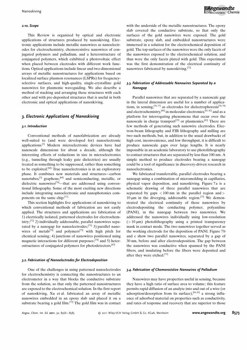
Figure 1a shows a modern ultramicrotome. Its compo-nents include a stereomicroscope, a movable stage that holdsthe knife, and a sample chuck (Figure 1 b) attached to amovable arm that holds the epoxy block. The movable armcontrols the fine positioning of the block and can advance insteps as small as 1 nm toward a single-crystalline diamondknife (Figure 1 c). The mechanism of fine control involves astepper motor connected to a spindle, and a lever thattransforms micrometer-length displacements of the spindleinto nanometer-length displacements of the arm.[50] The armand the epoxy block advance toward the knife in an ellipticalpath when viewed from the side, as drawn. The speed of
George M. Whitesides received his A.B.degree from Harvard University in 1960 andhis Ph.D. degree from the California Insti-tute of Technology in 1964. A MallinckrodtProfessor of Chemistry from 1982 to 2004,he is now a Woodford L. and Ann A. FlowersUniversity Professor. Prior to joining theHarvard faculty, he was a member of thechemistry faculty of the Massachusetts Insti-tute of Technology. His research interestsinclude physical and organic chemistry,materials science, biophysics, complexity, sur-face science, microfluidics, self-assembly,micro- and nanotechnology, and cell-surfacebiochemistry.
Figure 1. Photographs and schematic drawings of the tools of ultra-microtomy and nanoskiving. a) A photograph of a Leica UC6 ultra-microtome. b) A side view of the sample chuck and knife holder as theepoxy block impinges upon the knife. c) A top view of the single-crystalline diamond blade and the water-filled trough. Photographscourtesy of Dr. Ryan Chiechi. d) A schematic drawing of the sectioningprocess. The epoxy block contacts the diamond knife, and the offcut(the “slab”) slides onto the surface of water. The cutting processrepeats until the user stops the ultramicrotome or the embeddedmaterial is consumed. The water supports the slabs until the usercollects them.
Nanoskiving
8569Angew. Chem. Int. Ed. 2011, 50, 8566 – 8583 � 2011 Wiley-VCH Verlag GmbH & Co. KGaA, Weinheim www.angewandte.org
cutting is 0.1–10 mms�1, and produces sections at a rate of0.5–2 s�1.
2.3. The Process of Sectioning
Figure 1d is a schematic drawing of the process ofsectioning, which involves a complicated interplay ofevents: compression of the sample during the initiation ofcutting, and of the slab thereafter; tension perpendicular tothe plane of sectioning; generation of new surfaces; bending,as the slab reorients from vertical to horizontal; shearingstress (greatest in materials with low flexibility); friction ofthe slabs on the knife; and generation of heat.[55] The nascentepoxy slabs slide onto the surface of a water bath in the formof individual slabs or ribbons of connected slabs.[56]
There are two general mechanisms of the process ofsectioning proposed in the literature of ultramicrotomy:1) true sectioning, in which the edge of the knife maintainscontact with both the bottom surface of the nascent slab andthe facet of the block, and 2) crack initiation and propaga-tion.[57] True sectioning appears to dominate for metals andalloys. Characteristics of true sectioning include the appear-ance of shear lamellae and perpendicular to the direction ofcutting and concomitant compression along the same axis.Microtomed specimens—as well as micromachined chips ofmetal—exhibit these same characteristics.[48] Mechanismsresembling crack initiation and propagation appear tooperate in brittle materials, such as minerals and ceramics.[48]
The orientation of cleavage planes in crystalline samples alsodetermines the extent of fragmentation upon sectioningbrittle materials, as Antonovsky observed in samples ofalumina.[58] Malis found that true sectioning and crackinitiation and propagation can operate simultaneously ondifferent grains in the same sample, as he observed in sectionsof high-strength steel.[48]
2.4. The Embedding Medium
Most forms of ultramicrotomy—and all forms of nano-skiving—require an embedding medium to support theembedded structures during sectioning. In nanoskiving, theembedding medium also preserves the orientations of thenanostructures within the slabs. The embedding mediumshould have two properties, 1) a relatively high value ofelastic modulus (ca. 3 GPa; materials that are too compliantdeflect from the knife edge, rather than cleave), and 2) a highyield stress, after which the material undergoes plasticdeformation (ca. 70 MPa; otherwise the slab will deformupon sectioning).[55] Crosslinked epoxy resins fill most ofthese criteria at ambient temperatures, although it is possibleto section softer materials at cryogenic temperatures. Ourlaboratory has achieved excellent results with UVO-114(Epotek), which is UV-curable,[59] and good results withAraldite 502[60] and Epo-Fix (Electron Microscopy Scien-ces),[61] which are thermally curable. The newly cut surfaces ofthe epoxy slabs are smooth, with values of roughness (rms) ofapproximately 0.5 nm.[62]
2.5. Diamond Knives
The knife is the most important component of theultramicrotome. While glass knives are inexpensive anddisposable, the cutting edge degrades rapidly (after a fewuses). Our laboratory uses a 358 diamond knife, 1.8–2.4 mm inlength, whose edge has a radius of curvature of 3–6 nm.[63] Thecost of a knife is $2000–$3000. Knives must be re-sharpenedevery 6–12 months; this service is about half the cost of a newknife. In our experience, damage to the knife takes the formof chipping (rather than homogeneous “dulling”). Chips inthe knife cause scoring of the epoxy slabs in the direction ofcutting. Most scores are ten to a few hundred nm wide. Themost rapid deterioration of the quality of a knife we haveobserved occurred when sectioning thick films (ca. 500 nm) ofhard materials (e.g. Ti) and micron-scale ceramic objects (e.g.optical fibers). Significant chipping of the knife also occurswhen hard inorganic dust particles become inadvertentlyembedded in the epoxy blocks.
2.6. Nanoskiving Thin Films into Nanowires
The simplest embedded structure that can be sectionedusing nanoskiving is a metallic, ceramic, semiconducting,polymeric, or other planar thin film (Figure 2). Sectioning athin film produces a nanowire with a (roughly) rectangularcross section whose width is determined by the thickness ofthe film, and whose height is determined by the ultramicro-tome. To determine the applicability of different materials tonanoskiving, we performed a survey of thin films, depositedusing different methods: evaporation, sputter-coating, chem-ical-vapor deposition, electroless deposition, deposition in anelectrochemical cell, spin-coating, and solution-phase syn-thesis and subsequent deposition. The four major conclusionsare: 1) for evaporated, elemental films, soft and compliantmaterials (softer than platinum, or those with bulk values ofhardness < 500 MPa) tend to remain intact upon sectioning,while hard and stiff materials (harder than nickel) tend tofragment; 2) platinum and nickel are on the borderlinebetween soft and hard, for which the extent of fragmentationdepends on the method of deposition, and the morphology ofthe film; 3) the extent of fragmentation is higher when theorientation of the film is parallel to the direction of cuttingthan when the film is perpendicular to it; and 4) the speed ofcutting has no effect on the frequency of defects, from 0.1–10 mms�1 (which is consistent with Jesior�s observation thatthe cutting speed also has no effect on compression).[64,57] Wehave successfully formed nanostructures of aluminum,copper, silver, gold, lead, bismuth, palladium, platinum,nickel, germanium, silicon dioxide, all conducting and semi-conducting polymers tested, and films of lead sulfide nano-crystals. Figure 3 show examples of four classes of thin filmssuccessfully sectioned into nanowires that were intact over100 mm: metallic (gold, Figure 3a), ceramic (silicon dioxide,Figure 3b), semiconducting (germanium, Figure 3c), andpolymeric (poly(3-hexylthiophene) (P3HT), Figure 3d).
Figure 4 summarizes the results of the materials testedand makes predictions for materials we did not test or for
G. M. Whitesides et al.Reviews
8570 www.angewandte.org � 2011 Wiley-VCH Verlag GmbH & Co. KGaA, Weinheim Angew. Chem. Int. Ed. 2011, 50, 8566 – 8583

which we did not have enough data. We assumed all metallicthin films were evaporated or sputter-coated, and thuspolycrystalline. We assumed covalent solids (e.g., silicon andgermanium) were evaporated, and thus amorphous. Thedesignation “intact” indicates that the material did notfragment when sectioned. That is, these materials yielded
long unbroken nanowires (> 100 mm) when cutting perpen-dicular to the edge of the embedded thin film. We applied theterm “fragmented” to films that fractured extensively intosegments < 10 mm. We labeled films as “borderline” as thosewhose rate of fragmentation depended strongly on themethod of deposition, the size and geometry of the structure(e.g., nanowires or two-dimensional arrays of sub-micronparticles), and the orientation of the thin film with respect tothe direction of cutting. We designated all other materials inthe chart as either “predicted to be intact” or “predicted to befragmented” based on the probable mechanical properties ofa thin film of the material, and assumed i) that the film couldbe formed and ii) that it could be sectioned in an inertatmosphere. Interesting materials to which we have not yetapplied nanoskiving, or that we are just starting to explore,are those with internal porous or laminated structures (e.g.,graphite, montmorillonite, or block copolymers).
2.7. Combination of Nanoskiving with Photolithography
Patterning the thin film before embedding and sectioningcan produce structures more complex than single nanowires.Figure 5 summarizes a procedure that begins with photo-lithographic patterning of a thin metallic film into stripes on aflat epoxy wafer. The film can be patterned first on a siliconwafer and transferred to the epoxy,[65] or it can be patternedon the epoxy directly.[61] Sectioning these stripes produces acollinear array of nanowires.[65] The key result of the process isthat each dimension is determined precisely: the length byphotolithography, the width by the thickness of the evapo-rated film of gold, and the height by the set thickness of theultramicrotome. Section 4.2 describes the optical propertiesof monodisperse, collinear nanowires of gold.[65]
Figure 2. Summary of the process used for fabricating nanowires ofloosely defined length (>100 mm) by sectioning thin films. 1) A pieceof flat epoxy served as the substrate for deposition of a metallic,polymeric, semiconducting, or oxide film. 2) A rough cut provided astrip of this film supported by epoxy, 3) which we embedded inadditional epoxy. 4) Ultrathin sectioning (nanoskiving) and removal ofthe epoxy matrix formed nanowires in which each dimension wascontrolled by a different step of the process. Reproduced withpermission from Ref. [57]. Copyright 2010, American Chemical Society.
Figure 3. Examples of representative spans of nanowires of fourclasses of materials formed by obtaining sections of the metallic,ceramic, semiconducting, and polymeric thin films. Each nanowire isphysically continuous over >100 mm. Reproduced with permissionfrom Ref. [57]. Copyright 2010, American Chemical Society.
Figure 4. Summary of findings and predictions regarding the abilitiesof elements, oxides, polymers, and nanocrystals to form nanowires bysectioning thin films. Reproduced with permission from Ref. [57].Copyright 2010, American Chemical Society.
Nanoskiving
8571Angew. Chem. Int. Ed. 2011, 50, 8566 – 8583 � 2011 Wiley-VCH Verlag GmbH & Co. KGaA, Weinheim www.angewandte.org
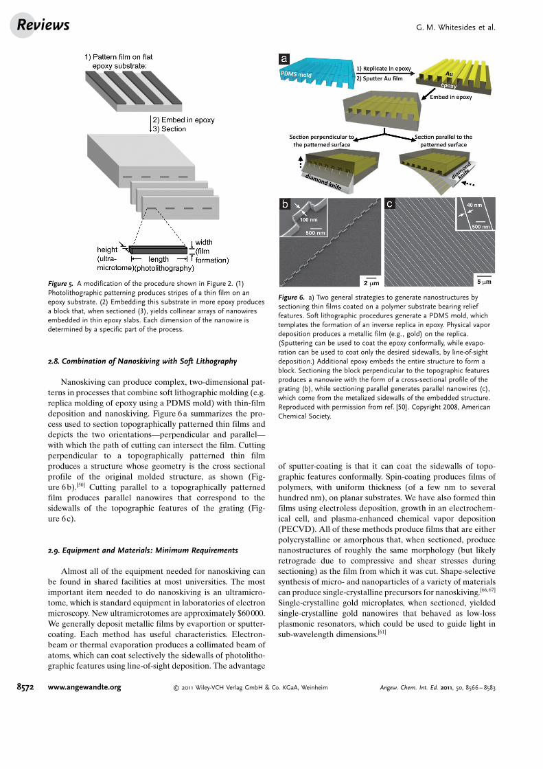
2.8. Combination of Nanoskiving with Soft Lithography
Nanoskiving can produce complex, two-dimensional pat-terns in processes that combine soft lithographic molding (e.g.replica molding of epoxy using a PDMS mold) with thin-filmdeposition and nanoskiving. Figure 6a summarizes the pro-cess used to section topographically patterned thin films anddepicts the two orientations—perpendicular and parallel—with which the path of cutting can intersect the film. Cuttingperpendicular to a topographically patterned thin filmproduces a structure whose geometry is the cross sectionalprofile of the original molded structure, as shown (Fig-ure 6b).[50] Cutting parallel to a topographically patternedfilm produces parallel nanowires that correspond to thesidewalls of the topographic features of the grating (Fig-ure 6c).
2.9. Equipment and Materials: Minimum Requirements
Almost all of the equipment needed for nanoskiving canbe found in shared facilities at most universities. The mostimportant item needed to do nanoskiving is an ultramicro-tome, which is standard equipment in laboratories of electronmicroscopy. New ultramicrotomes are approximately $60000.We generally deposit metallic films by evaportion or sputter-coating. Each method has useful characteristics. Electron-beam or thermal evaporation produces a collimated beam ofatoms, which can coat selectively the sidewalls of photolitho-graphic features using line-of-sight deposition. The advantage
of sputter-coating is that it can coat the sidewalls of topo-graphic features conformally. Spin-coating produces films ofpolymers, with uniform thickness (of a few nm to severalhundred nm), on planar substrates. We have also formed thinfilms using electroless deposition, growth in an electrochem-ical cell, and plasma-enhanced chemical vapor deposition(PECVD). All of these methods produce films that are eitherpolycrystalline or amorphous that, when sectioned, producenanostructures of roughly the same morphology (but likelyretrograde due to compressive and shear stresses duringsectioning) as the film from which it was cut. Shape-selectivesynthesis of micro- and nanoparticles of a variety of materialscan produce single-crystalline precursors for nanoskiving.[66,67]
Single-crystalline gold microplates, when sectioned, yieldedsingle-crystalline gold nanowires that behaved as low-lossplasmonic resonators, which could be used to guide light insub-wavelength dimensions.[61]
Figure 5. A modification of the procedure shown in Figure 2. (1)Photolithographic patterning produces stripes of a thin film on anepoxy substrate. (2) Embedding this substrate in more epoxy producesa block that, when sectioned (3), yields collinear arrays of nanowiresembedded in thin epoxy slabs. Each dimension of the nanowire isdetermined by a specific part of the process.
Figure 6. a) Two general strategies to generate nanostructures bysectioning thin films coated on a polymer substrate bearing relieffeatures. Soft lithographic procedures generate a PDMS mold, whichtemplates the formation of an inverse replica in epoxy. Physical vapordeposition produces a metallic film (e.g., gold) on the replica.(Sputtering can be used to coat the epoxy conformally, while evapo-ration can be used to coat only the desired sidewalls, by line-of-sightdeposition.) Additional epoxy embeds the entire structure to form ablock. Sectioning the block perpendicular to the topographic featuresproduces a nanowire with the form of a cross-sectional profile of thegrating (b), while sectioning parallel generates parallel nanowires (c),which come from the metalized sidewalls of the embedded structure.Reproduced with permission from ref. [50]. Copyright 2008, AmericanChemical Society.
G. M. Whitesides et al.Reviews
8572 www.angewandte.org � 2011 Wiley-VCH Verlag GmbH & Co. KGaA, Weinheim Angew. Chem. Int. Ed. 2011, 50, 8566 – 8583
2.10. Scope
This Review is organized by optical and electronicapplications of structures produced by nanoskiving. Elec-tronic applications include metallic nanowires as nanoelectr-odes for electrochemistry, chemoresistive nanowires of con-jugated polymers and palladium, and a heterostructure ofconjugated polymers, which exhibited a photovoltaic effectwhen placed between electrodes with different work func-tions. Optical applications include linear and two-dimensionalarrays of metallic nanostructures for applications based onlocalized surface plasmon resonances (LSPRs) for frequency-selective surfaces, and high-quality, single-crystalline goldnanowires for plasmonic waveguiding. We also describe amethod of stacking and arranging these structures with eachother and with pre-deposited structures that is useful in bothelectronic and optical applications of nanoskiving.
3. Electronic Applications of Nanoskiving
3.1. Introduction
Conventional methods of nanofabrication are alreadywell-suited to (and were developed for) nanoelectronicapplications.[5] Modern microelectronic devices have hadnanoscale dimensions for about a decade, although theinteresting effects of reductions in size in microelectronics(e.g., tunneling through leaky gate dielectrics) are usuallytreated as something to be suppressed, rather than somethingto be exploited.[68] True nanoelectronics is in an exploratoryphase. It combines new materials and structures—carbonnanotubes,[3] graphene,[69] and semiconducting, metallic, ordielectric nanowires[70]—that are addressed using conven-tional lithography. Some of the most exciting new directionsinclude integrating nanoelectronic and nanophotonics com-ponents on the same chip.[71]
This section highlights five applications of nanoskiving towhich conventional methods of fabrication are not easilyapplied. The structures and applications are fabrication of1) electrically isolated, patterned electrodes for electrochem-istry;[72] 2) individually addressable, parallel nanowires sepa-rated by a nanogap for nanoelectrodes;[73] 3) parallel nano-wires of metals[74] and polymers[75] with high pitch forchemical sensing; 4) junctions of nanowires positioned usingmagnetic interactions for different purposes;[74] and 5) heter-ostructures of conjugated polymers for photodetectors.[62]
3.2. Fabrication of Nanoelectrodes for Electrodeposition
One of the challenges in using patterned nanoelectrodesfor electrochemistry is connecting the nanostructures to anelectrometer in a way that blocks the conductive substratefrom the solution, so that only the patterned nanostructuresare exposed to the electrochemical solution. In the first reportof nanoskiving, Xu et al. fabricated an array of metallicnanowires embedded in an epoxy slab and placed it on asubstrate bearing a gold film.[72] The gold film was in contact
with the underside of the metallic nanostructures. The epoxyslab covered the conductive substrate, so that only thesurfaces of the gold nanowires were exposed. The goldsubstrate, epoxy slab, and embedded nanostructures wereimmersed in a solution for the electrochemical deposition ofgold. The top surfaces of the nanowires were the only facets ofthe nanowires exposed to the electrochemical solution, andthus were the only facets plated with gold. This experimentwas the first demonstration of the electrical continuity ofnanowires fabricated by nanoskiving.[72]
3.3. Fabrication of Addressable Nanowires Separated by aNanogap
Parallel nanowires that are separated by a nanoscale gapin the lateral dimension are useful for a number of applica-tions, in sensing,[76, 77] as electrodes for dielectrophoresis[78,79]
and electrochemistry,[80] in molecular electronics,[81, 82] and as aplatform for interrogating phenomena that occur over thenanoscale in charge transport[35] or plasmonics.[83] There arefew methods of generating such nanowire electrodes. Elec-tron-beam lithography and FIB lithography and milling aretwo such methods, but, in addition to the usual drawbacks ofhigh cost, inconvenience, and low throughput, it is difficult toproduce nanoscale gaps over large lengths. It is nearlyimpossible in an academic laboratory to use photolithographyto contact structures that are separated by less than 100 nm. Asimple method to produce electrodes bearing a nanogapcould be a tool of significance in discovery-driven research innanoelectronics.
We fabricated transferrable, parallel electrodes bearing ananogap using a combination of micromolding in capillaries,physical vapor deposition, and nanoskiving. Figure 7a is aschematic drawing of three parallel nanowires that areseparated by gaps < 100 nm in the parallel region and>10 mm in the diverging, addressable region.[73] We demon-strated the electrical continuity of these nanowires byelectrodepositing the conducting polymer, polyaniline(PANI), in the nanogap between two nanowires. Weaddressed the nanowires individually using low-resolution(> 10 mm) photolithography using a printed transparencymask in contact mode. The two nanowires together served asthe working electrode for the deposition of PANI. Figure 7band c show two parallel nanowires, separated by a gap of30 nm, before and after electrodeposition. The gap betweenthe nanowires was conductive when spanned by the PANIfibers, and insulating before the fibers were deposited andafter they were etched.[73]
3.4. Fabrication of Chemoresistive Nanowires of Palladium
Nanowires may have properties useful in sensing, becausethey have a high ratio of surface area to volume; this featurepermits rapid diffusion of an analyte into and out of a wire (oradsorption/desorption from its surface),[84, 85] a strong influ-ence of adsorbed material on properties such as conductivity,and rates of response and recovery that are superior to those
Nanoskiving
8573Angew. Chem. Int. Ed. 2011, 50, 8566 – 8583 � 2011 Wiley-VCH Verlag GmbH & Co. KGaA, Weinheim www.angewandte.org

of devices based on thin films or fibrous networks. Palladiumis an example of a material having properties useful in sensingbecause of its resistance to oxidation and reproducible loss inconductivity (chemoresistivity) upon absorption of hydrogen.(It is also soft enough to be sectioned with the ultramicrotomewithout fragmentation). Penner and coworkers have fabri-cated and studied palladium nanowires and their character-istics as hydrogen gas sensors.[86] These nanowires can beprepared by templated electrodeposition,[77] or by step-edgedecoration of highly oriented pyrolytic graphite, or othertemplates.[87] We have fabricated palladium nanowires withrectangular cross sections and high pitch using a sequence oftwo steps: iterative template stripping,[88] followed by nano-skiving.[74]
To characterize the nanowires electrically, we tested themfor function as sensors for hydrogen gas. We began by placingan epoxy slab bearing five palladium nanowires (w = 60 nm,h = 80 nm) on an insulating substrate. We then deposited goldelectrodes through a stencil mask to define a span of 10 mm(Figure 7d). Etching the epoxy matrix freed the sides of thenanowires. Figure 7e shows three plots of current density vs.applied voltage. The first, “native”, represents the conduc-tivity of the nanowires in the ambient atmosphere of thelaboratory. The second, “H2”, represents the lower conduc-tivity of the nanowire when exposed to a stream of hydrogengas. The third, “ctrl”, is a control experiment, in which weexposed the nanowires to a stream of air. The controlexperiment and the native conductivity of the nanowires
exhibited identical electrical characteristics. From the value ofcurrent at 10 mV and the dimensions of the nanowires, wecalculated the conductivity of the nanowires to be 2.4 �104 W�1 cm�1. For comparison, the conductivity of bulkpalladium is 9.5 � 104 W�1 cm�1.
3.5. Fabrication of Chemoresistive Conjugated PolymerNanowires
Organic semiconductors are a class of materials whoseproperties (e.g., reversible behavior in cycles of oxidation andreduction, and modifiable conductivity by electrical gating)render them potentially attractive for chemical and biologicalsensing.[89] Incorporation of molecular recognition elementsinto semiconducting, conjugated polymer nanowires is rela-tively straightforward by synthesis, while modifications ofcarbon nanotubes and inorganic nanowires require function-alization of the surfaces, carried out post-fabrication.[90] Otherpossible uses for conjugated polymer nanowires are as toolsfor studying one-dimensional charge transport,[91] or as field-effect transistors,[92] actuators[93] or interconnects.[94]
There is not yet a truly general technique for thefabrication of conjugated polymer nanowires. Examples ofmethods that satisfy some of the criteria of cost, accessibility,and applicability to different materials, are electrodepositionin templates,[77] dip–pen nanolithography,[44] nanoimprintlithography,[95] and electrospinning[96]—a well-studied tech-nique that can produce mats or aligned collections ofnanowires.[96] Craighead and coworkers have used scannedelectrospinning[97] to deposit single nanowires of polyani-line[98] and poly(3-hexylthiophene)[92] on a rotating substrate,while Xia and coworkers have developed an approach todeposit uniaxial collections of nanofibers of a range ofinorganic and organic materials.[99, 100]
Using a procedure that involves stacking spin-coated filmsof conjugated polymers, followed by nanoskiving, we havegenerated nanowires with rectangular cross sections individ-ually, in bundles, or in parallel, with high pitch.[75] We beganby spin-coating two conjugated polymers, poly(benizimidazo-benzophenantrholine) ladder (BBL) and poly(2-methoxy-5-(2’-ethylhexyloxy)-1,4-phenylenevinylene) (MEH-PPV)alternately on the same substrate, such that fifty 100 nm-thick layers of BBL were separated by fifty 100 nm-thicklayers of MEH-PPV. Release of this free-standing, 10 mm-thick film, and subsequent sectioning perpendicular to theplane of the layers, provided a cross section which bore100 nm-wide strips of the two conjugated polymers. Etchingthe MEH-PPV with an air plasma left behind parallel BBLnanowires (Figure 8a and b), and dissolving BBL in meth-anesulfonic acid left behind MEH-PPV nanowires (Figure 8cand d). Figure 8 e is a plot of current density vs. voltage (J–V)of a group of MEH-PPV nanowires, of the type shown inFigure 8d, when exposed to I2 vapor.
Figure 7. a) A schematic drawing of three parallel, addressable goldnanowires. b) Parallel gold nanowires separated by a 30 nm gap.c) The same gold nanowires after electrochemical deposition ofpolyaniline. Reproduced with permission from ref. [73]. Copyright2008, American Chemical Society. d) A group of five parallel nanowiresof palladium spanning a 10 mm gap between Au electrodes. e) Theelectrical response of the nanowires in their native state, when exposedto a stream of hydrogen gas, and a control experiment in which thenanowire was exposed to a stream of compressed air.
G. M. Whitesides et al.Reviews
8574 www.angewandte.org � 2011 Wiley-VCH Verlag GmbH & Co. KGaA, Weinheim Angew. Chem. Int. Ed. 2011, 50, 8566 – 8583

3.6. Arranging Nanowires of Different Types Using MagneticMooring
One of the central challenges in promoting discoveriesof nanoscience into technological applications is theability to manipulate and position nanostructures on asurface. We refer specifically to nanostructures fabricatedby bottom-up methods, such as solution-phase synthesis[66]
or vapor-liquid-solid growth[70] (structures fabricated bytop-down procedures are usually formed where thetemplate provided by the photomask dictates). The usualprocedure to interrogate a nanostructure prepared bybottom-up synthesis is to deposit structures randomly, andthen to select a serendipitously positioned structure—forexample, a nanowire spanning two electrodes, or situatedin the proper orientation on an optical waveguide. Themore elements that make up a system—e.g., nanowires,waveguides, electrodes, and quantum dots—the lower theprobability that random assembly can generate a usefulgeometry. This section focuses on one-dimensional struc-tures[3] but the processes we describe would be applicableto other structures as well.
There are several methods of aligning nanowires ingroups and individually. Methods to align nanowires ingroup include shear alignment of nanowires suspended influids,[101–105] including wafer-scale alignment in bubble-blown films;[106] brushing suspensions of nanowires over alithographically patterned substrate to create highly
aligned regions of nanowires on exposed areas;[107] andalignment of nanowires in a Langmuir-Blodgett trough.[108]
Methods of positioning single nanowires include opticaltweezing[109] and opto-electronic tweezing;[110] methods ofmanipulation by direct contact with scanning probe tips[111]
and micromanipulators;[112] and electrophoretic alignment ofover pre-patterned electrodes.[113]
In nanoskiving, the generation of the thin slabs—usuallyremoved in the final step of fabrication—is one of the mostuseful characteristics of the technique. The slabs are visible,manipulable objects that can be overlayed—along with thenanostructures they contain—with structures on the sub-strate. Complex structures embedded in the polymer slabretain their orientation during manipulations of the slab. Forstructures formed by laying slabs on top of one another, wehave developed a procedure that combines nanoskiving withnon-contact, magnetic manipulation of the slabs (“magneticmooring”, Figure 9). The key step in magnetic mooring is co-embedding ferromagnetic particles (we used nickel films or
Figure 8. a) BBL nanowires before (bottom right) and after (topleft) etching the sacrificial polymer, MEH-PPV, with an air plasma.The unetched region was protected with a conformal slab ofPDMS. b) A group of 50 parallel BBL nanowires with 200 nm pitch.c) A single MEH-PPV nanowire with a square cross section of100 nm � 100 nm. d) A group of fifty MEH-PPV nanowires.e) A J–V plot of the MEH-PPV nanowires in (d) doped by iodine(I2) vapor. Reproduced with permission from ref. [75]. Copyright2008, American Chemical Society.
Figure 9. a) Schematic representations of the methods used for fabrication (I. Nano-skiving) and positioning (II. Magnetic Mooring) of nanowires. Single-crystalline (b)and polycrystalline (c) gold nanowires fabricated using nanoskiving and positionedusing magnetic mooring. Reproduced with permission from ref. [74]. Copyright 2009,American Chemical Society.
Nanoskiving
8575Angew. Chem. Int. Ed. 2011, 50, 8566 – 8583 � 2011 Wiley-VCH Verlag GmbH & Co. KGaA, Weinheim www.angewandte.org

powder) with the metallic or polymeric nanostructures to bepositioned. In an initial demonstration of magnetic mooring,we transferred slabs containing nickel particles and goldnanowires to a substrate, along with � 5 mL of water. Theslabs floated on the surface of a drop of water, and were thusmobile under the influence of an external permanent magnetattached to a micromanipulator (Figure 9a). As the waterevaporated, the slabs, along with the nanostructures theycontained, deposited on (and adhered to) the substrate, withan average deviation from the intended position of 16 mm.This registration is crude, but useful in some applications.Figure 9b and c show crossing single-crystalline and poly-crystalline gold nanowires.
To show that it was possible to form electrically contin-uous junctions between nanowires of different types, weplaced a single nanowire of poly(3-hexylthiophene) perpen-dicularly across the gap between two parallel gold nanowires.This geometry could be useful in measuring nanoscale chargetransport in optoelectronic polymers, and in the fabrication ofchemical sensors[114] or field-effect transistors based on singlenanowires.[92] We deposited two parallel gold nanowires,which were embedded in the same epoxy slab. Separately, wefabricated a poly(3-hexylthiophene) nanowire (100 nm �100 nm cross section), co-embedded with nickel powder inepoxy, positioned it to span the 50 mm gap between goldnanowires. Poly(3-hexylthiophene) undergoes an insulator-to-metal transition upon exposure to I2.
[115] Electrical meas-urements of the polymer nanowire—using the gold nanowiresas electrodes—could detect the presence or absence of a solidpiece of I2 placed in the vicinity of the nanowire. It should alsobe possible to use this technique for four-terminal measure-ments, which would allow decoupling of the contact resistancefrom the true resistance of a nanowire.[84]
3.7. Fabrication of an Ordered Bulk Heterojunction ofConjugated Polymers
Nanoskiving is one of a few techniques for nanoscalepatterning in which features can be made of differentmaterials, and in which components fabricated in differentmaterials touch in the lateral dimension. Forming denselypacked features that touch laterally may be able to address along-standing problem in organic photovoltaic cells: that is, tofabricate a structure in which two organic semiconductors(electron-donating and electron-accepting) are laterally sep-arated on the scale of exciton diffusion, or approximately10 nm.[116] A persistent challenge in the fabrication of organicphotovoltaic devices is that the distance an exciton can travelbefore it decays (the exciton diffusion length, or LD) is about10 times shorter than the thickness of material required forefficient absorption of photons (100 to 200 nm). The archi-tecture that satisfies the requirement that both LD and thethickness for optimal absorption of light is known as theordered bulk heterojunction.[117] It has a cross section ofelectron-donating and electron-accepting phases that isintermixed on the length scale of LD and is 100 to 200 nmthick.
We used nanoskiving to fabricate an ordered bulkheterojunction of two conjugated polymers. The process hadthree steps: 1) spin-coating a composite film with 100 alter-nating layers of BBL (e-acceptor) and MEH-PPV (e-donor);2) rolling this multilayer film into a cylinder (a “jelly roll”);and 3) nanoskiving the jelly roll.[62] The cross-section of a slabof the jelly roll had an interdigitated arrangement of the twopolymers. The thickness of the slab was determined by theultramicrotome and the spacing between the two materialswas determined by the details of the spin-coating. We placed aslice of the jelly roll between two electrodes with differentwork functions (Figure 10 a), tin-doped indium oxide (ITO)and eutectic gallium-indium (EGaIn), and observed a photo-voltaic response when we irradiated the stack with white light(10 b). Selective excitation of BBL (which does not produce aphotovoltaic response by itself) with red light (which MEH-PPV does not absorb) confirmed that the photovoltaic effectwas the result of photoinduced charge transfer between BBLand MEH-PPV. Although the power conversion efficiency ofthese structures were low (< 0.1%), we believe that thisapproach to fabricating donor/acceptor heterojunctions couldbe useful in photophysical studies, and might ultimatelysuggest new approaches to OPV devices.[62]
4. Optical Applications of Nanoskiving
4.1. Introduction
Metallic nanostructures with well-defined nano andmicroscale geometries are the building blocks of the branch
Figure 10. a) A schematic drawing of a heterojunction (“jelly roll”) ofconjugated polymers sandwiched between two electrodes with asym-metric work functions. b) Upon irradiation with white light, thejunction produced a photovoltaic effect. Reproduced with permissionfrom ref. [62]. Copyright 2008, Wiley-VCH GmbH & Co. KGaA.
G. M. Whitesides et al.Reviews
8576 www.angewandte.org � 2011 Wiley-VCH Verlag GmbH & Co. KGaA, Weinheim Angew. Chem. Int. Ed. 2011, 50, 8566 – 8583

of optics known as plasmonics.[118, 119] A surface plasmon is aquantum of oscillation of charge at a metal-dielectric inter-face, driven by electromagnetic radiation. Localized surfaceplasmon resonances (LSPRs) can be excited in nanoparticleswhose dimensions are much smaller than the wavelength ofexcitation. The energy of the LSPR is a function of the sizeand shape of the particle, and its dielectric environment.[118]
Applications of plasmonic nanoparticles include opticalfilters;[120, 121] substrates for optical detection of chemical andbiological analytes using LSPRs[122] or surface-enhancedRaman scattering (SERS);[123–125] substrates for enhancedluminosity;[126] materials to augment absorption in thin-filmphotovoltaic devices;[127] metamaterials[7, 128] with negativemagnetic permeabilities[129] and refractive indices;[130] andmaterials for perfect lenses,[131] and invisibility cloaking.[132]
The most sophisticated arrays of plasmonic structures arefabricated using EBL,[133] FIB,[130] or direct laser writing.[134]
There are also a number of chemical, soft lithographic, andother unconventional approaches to producing plasmonicmaterials.[119] Solution-phase synthesis can produce single-crystalline metallic structures of different shapes and materi-als.[66, 135] Nanosphere lithography, pioneered by Van Duyneand coworkers, uses self-assembled spheres as a stencil mask,in which the void spaces between the spheres direct thedeposition of metal on the substrate by evaporation.[136,137]
Rogers, Odom, Nuzzo, and coworkers have used soft litho-graphic techniques, such as patterning photoresists withconformal phase-shifting masks,[138] as well as soft nano-imprint lithography,[139] to form arrays of nanoholes inmetallic films[140] and pyramidal shells.[141] This sectiondescribes the use of nanoskiving to generate nanostructuresfor a variety of optical applications.
4.2. Fabrication of Gold Nanowires and Size-Dependent SurfacePlasmon Resonance
The combination of patterning or molding, thin-filmdeposition, and sectioning can control each dimension ofthe structures produced by nanoskiving.[50] Plasmonic appli-cations—e.g., sensors based on changes in the frequency ofLSPRs, optical polarizers, filters—require uniform absorptionacross arrays of particles. Monodisperse particles satisfy thisrequirement, while polydisperse particles absorb broadly.[2]
Figure 5 (Section 2.7) summarizes a method to fabricatecollinear arrays of optically indistinguishable nanowires ofgold that uses nanoskiving.[65] The cross sections of thenanowires had dimensions as small as 10 nm � 30 nm; allnanowires were 2 mm long.
Illumination of groups of these nanowires excited plas-mon resonances along their transverse axes. In order to testthe optical homogeneity of the nanowires, Xu et al. collectedthe spectra of four nanowires individually. The nanowiresexhibited overlapping spectra of scattered light, whichimplied that they were geometrically monodisperse. Therewas a red shift in the peak of the scattered intensity withincreasing height. This observation was consistent with finite-difference time-domain (FDTD) simulations. The ability to
tune the size, shape, and composition of metallic structures isa useful capability of nanoskiving for optical applications.[65]
4.3. Fabrication of Single-Crystalline Gold Nanowires forPlasmonic Waveguiding
Nanophotonic devices, including photonic integratedcircuits, require waveguiding of optical energy in sub-wave-length dimensions.[7, 142] Patterned metal strips or can guidelight using surface plasmon polaritons (SPPs) that propagatealong a metal-dielectric interface, but efforts to produceefficient plasmonic waveguides from these structures havebeen hindered by the rough surfaces of polycrystallineevaporated films, which are unsuitable to support propagationof the lengths needed.[143] Recently, Ditlbacher and cow-orkers,[144] and others,[145] have shown that high quality, single-crystalline silver nanowires can confine the energies ofincident photons to propagating SPPs, which travel alongthe longitudinal axes of the nanowires (in Section 4.2, LSPRswere excited along the transverse axes). For example, micro-fabricated strips of silver exhibited propagation lengths of2.5 mm, where single crystalline silver nanowires have prop-agation lengths of 10 mm, due to the low losses at the smoothsurface.[144] Gold nanowires might be superior to silvernanowires for practical applications, because gold is stablein air. Studies of SPPs along gold nanowires had not beenperformed, however, in part because the synthesis of silvernanowires was well established.[146]
Using a procedure that combined chemical synthesis ofgold microplates[147] and nanoskiving (Figure 11 a), we wereable to produce collinear arrays of high quality, singlecrystalline nanowires.[61] Figure 11 b shows a dark-field opticalimage and Figure 11 c shows an SEM image. In order todetermine if these nanowires could be used to confine andguide light using SPPs, we mounted a nanowire on a prism andilluminated it with unpolarized white light under total internalreflection. We oriented the nanowire parallel to the evan-escent wave generated by at the surface of the prism(Figure 11 d). We observed light scattering from both ends(“input” and “output”) of the nanowire; Figure 11 e shows thespectra of wavelengths scattered from each end. The minimaof the spectrum scattered from the input tip, and the maximaof the spectrum scattered from the output tip, correspondedto wavelengths at which maximum coupling of the light intothe nanowire occurred due to constructive interference of theSPP modes reflecting between the two tips. These wave-lengths correspond to those that reproduced themselves aftera full round trip. The light did not scatter from the center ofthe nanowire because the wave vector of the surface plasmonis higher than that of light in air.[61]
These single-crystalline plasmonic waveguides could bestacked on top of each other, or positioned on microfabri-cated polymeric waveguides, using magnetic mooring, asdescribed in section 3.6.[74] This process could be used togenerate more complex arrangements of elements in order toproduce multicomponent photonic devices comprising, forexample, photonic and plasmonic waveguides,[142] semicon-ductor nanowires,[71] and single-photon emitters.[7]
Nanoskiving
8577Angew. Chem. Int. Ed. 2011, 50, 8566 – 8583 � 2011 Wiley-VCH Verlag GmbH & Co. KGaA, Weinheim www.angewandte.org

4.4. Fabrication of 2D Arrays of Nanostructures
Sections 4.2 and 4.3 focused on one-dimensional nano-structures. Applications such as optical filters,[120, 121] sub-strates for surface-enhanced Raman spectroscopy,[8,123] andmetamaterials[128,130, 133, 137] required two-dimensional arrays ofnanostructures. Using a procedure that combined replicamolding of a nanostructured template (for example, a set ofnanorods) in epoxy by soft lithography, thin-film deposition ofmetal onto those rods, embedding, and sectioning parallel tothe plane supporting the nanorods, we produced two-dimen-sional arrays of nanostructures using nanoskiving. Figure 12outlines an example. First, we formed an array of epoxynanoposts by soft lithographic molding. This array was coatedconformally with gold by sputter coating, then coated bypolypyrrole (PPy) using electrochemical growth, then coateda second time with gold by sputter coating. These procedures
produced an array of three-layered, coaxial nanoposts withradial symmetry. When these composite posts were embed-ded in epoxy and sectioned into slabs, the slabs comprised anarray of features with radial symmetry: discs of epoxy, andconcentric rings of gold, PPy, and gold. These arrays could betransferred to essentially any substrate. An optional step wasto remove the organic components by etching using an airplasma. Etching left behind arrays of free-standing, concen-tric rings of gold. Figure 13a–h show a series of structuresfabricated by this and related procedures.
There are at least five important aspects of the structuresproduced by this procedure that cannot be replicated easily, ifat all, with other techniques: 1) the linewidths of thestructures are determined by the thickness of the thin film,not the dimensions of the original topographic master, and
Figure 11. a) Schematic representation of the procedure used to deposit, embed,and section gold microplates into nanowires. b) Dark-field and c) SEM images ofa group of colinear single-crystalline nanowires. d) Schematic drawing of theorientation of the nanowire on a prism with respect to the wave vector (k) of theimpinging white light. e) Spectra of scattered light from both the input andoutput tips of the nanowires. The minima of the input and the maxima of theoutput intensities correspond to the wavelengths of maximum coupling into thenanowire (Fabry-Perot resonance). f) Scattering spectra of a polycrystalline nano-wire fabricated by photolithography, evaporation, and nanoskiving. The spectrado not exhibit evidence of propagating resonator modes.
Figure 12. Summary of the procedure used to fabricate concentricrings by thin film deposition and thin sectioning of high-aspect-rationanoposts. Sputter-coating produced a film of Au on an array of epoxynanoposts (step 1). This film served as the working electrode for theconformal electrodeposition of PPy (step 2). A second sputter-coatingprovided a nanopost array with a core-shell-core-shell composition(step 3). Embedding this structure in additional epoxy formed a block(step 4). Sectioning this block with the ultramicrotome yielded anepoxy slab containing the nanostructures (step 5). This structure couldbe transferred from the water bath on which the nanostructures floatto any substrate (not shown). Treatment with an air plasma simulta-neously etched the epoxy matrix and the PPy in between the Au rings(step 6). Reproduced with permission from ref. [59]. Copyright 2010,American Chemical Society.
G. M. Whitesides et al.Reviews
8578 www.angewandte.org � 2011 Wiley-VCH Verlag GmbH & Co. KGaA, Weinheim Angew. Chem. Int. Ed. 2011, 50, 8566 – 8583
thus the nanoscale dimensions do not need to be encodedby EBL or FIB to appear in the final structure; 2) the heightof the structures can be tuned over a large range (80 nm–2 mm demonstrated in Figure 13b and c), simply by chang-ing the thickness of the slabs cut by the ultramicrotome; 3)the structures can comprise two or more materials in thesame plane, in a single step of replication; 4) the compo-nents can be in physical contact in the lateral dimension;and 5) many slabs may be obtained from a single embeddedstructure (we have produced as many as 60 consecutive
cross sections, 100 nm thick, from a single embedded array of8 mm, gold-coated epoxy nanoposts).[59]
4.5. Plasmonic Properties of Two-Dimensional Arrays ofNanostructures
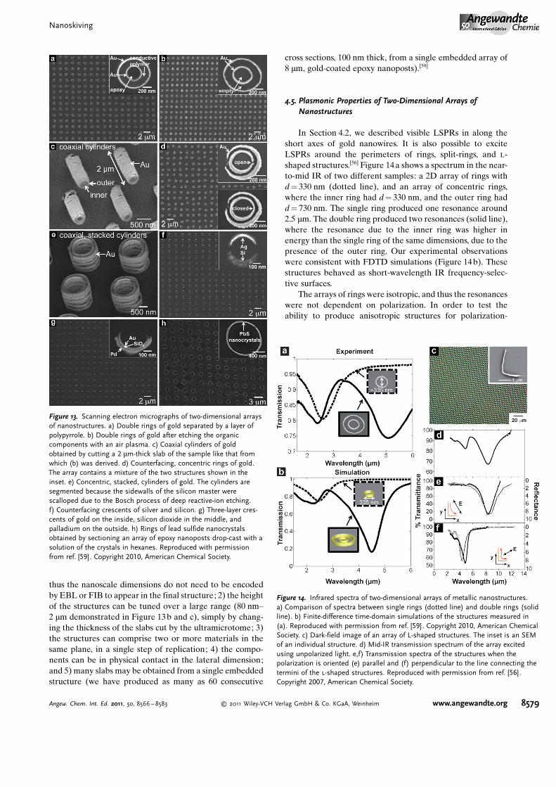
In Section 4.2, we described visible LSPRs in along theshort axes of gold nanowires. It is also possible to exciteLSPRs around the perimeters of rings, split-rings, and l-shaped structures.[56] Figure 14 a shows a spectrum in the near-to-mid IR of two different samples: a 2D array of rings withd = 330 nm (dotted line), and an array of concentric rings,where the inner ring had d = 330 nm, and the outer ring hadd = 730 nm. The single ring produced one resonance around2.5 mm. The double ring produced two resonances (solid line),where the resonance due to the inner ring was higher inenergy than the single ring of the same dimensions, due to thepresence of the outer ring. Our experimental observationswere consistent with FDTD simulations (Figure 14 b). Thesestructures behaved as short-wavelength IR frequency-selec-tive surfaces.
The arrays of rings were isotropic, and thus the resonanceswere not dependent on polarization. In order to test theability to produce anisotropic structures for polarization-
Figure 13. Scanning electron micrographs of two-dimensional arraysof nanostructures. a) Double rings of gold separated by a layer ofpolypyrrole. b) Double rings of gold after etching the organiccomponents with an air plasma. c) Coaxial cylinders of goldobtained by cutting a 2 mm-thick slab of the sample like that fromwhich (b) was derived. d) Counterfacing, concentric rings of gold.The array contains a mixture of the two structures shown in theinset. e) Concentric, stacked, cylinders of gold. The cylinders aresegmented because the sidewalls of the silicon master werescalloped due to the Bosch process of deep reactive-ion etching.f) Counterfacing crescents of silver and silicon. g) Three-layer cres-cents of gold on the inside, silicon dioxide in the middle, andpalladium on the outside. h) Rings of lead sulfide nanocrystalsobtained by sectioning an array of epoxy nanoposts drop-cast with asolution of the crystals in hexanes. Reproduced with permissionfrom ref. [59]. Copyright 2010, American Chemical Society.
Figure 14. Infrared spectra of two-dimensional arrays of metallic nanostructures.a) Comparison of spectra between single rings (dotted line) and double rings (solidline). b) Finite-difference time-domain simulations of the structures measured in(a). Reproduced with permission from ref. [59]. Copyright 2010, American ChemicalSociety. c) Dark-field image of an array of L-shaped structures. The inset is an SEMof an individual structure. d) Mid-IR transmission spectrum of the array excitedusing unpolarized light. e,f) Transmission spectra of the structures when thepolarization is oriented (e) parallel and (f) perpendicular to the line connecting thetermini of the l-shaped structures. Reproduced with permission from ref. [56].Copyright 2007, American Chemical Society.
Nanoskiving
8579Angew. Chem. Int. Ed. 2011, 50, 8566 – 8583 � 2011 Wiley-VCH Verlag GmbH & Co. KGaA, Weinheim www.angewandte.org
dependent applications, Xu et al. produced the L-shapedstructures in Figure 14c by a combination of molding andline-of-sight deposition of gold.[56] Figure 14 d shows theresonance of the array in response to unpolarized light. Itconsists of two distinct modes. The mode at 8.4 mm was due toan oscillation in a line that connects the two termini of the L,and was excited by linearly polarized light that was parallel tothat line (Figure 14 e). The mode at 4.8 mm was excited bylight polarized perpendicular to the line that connects the twoends of the L (Figure 14 f). This polarization bisected thestructure and produced two orthogonal regions that oscillatedin phase. These observations were again consistent withFDTD simulations.[56]
4.6. Integration of Plasmonic Arrays with Optical Fibers
The thin slab of epoxy in which the structures produced bynanoskiving are embedded provides a visible handle totransfer arrays to substrates.[59] There is, thus, a majorchallenge in optics to which nanoskiving seems particularly(perhaps uniquely) well-suited—modifying the cleaved facetsof optical fibers with arrays of nanostructures. The ability tocontrol the emission from fibers using filters or polarizers, orthe fabrication of sensors for in situ, label-free detection ofchemical or biological analytes using either SERS[148] orLSPRs,[149] are possible applications of modified opticalfibers.[150] Attachment of plasmonic arrays to (or formationon) the cleaved facets of fibers is not straightforward byconventional means, however. Photolithographic patterningof the facets of fibers would require deposition, exposure anddevelopment of photoresist on a small area (d� 100 mm), withthe fiber somehow positioned correctly.[24] Examples ofunconventional methods to integrate plasmonic elementswith optical fibers include anisotropic chemical etching, toform arrays of sharp cones,[151] and transferring gold structuresfabricated by EBL from a surface to which gold adheredweakly.[124]
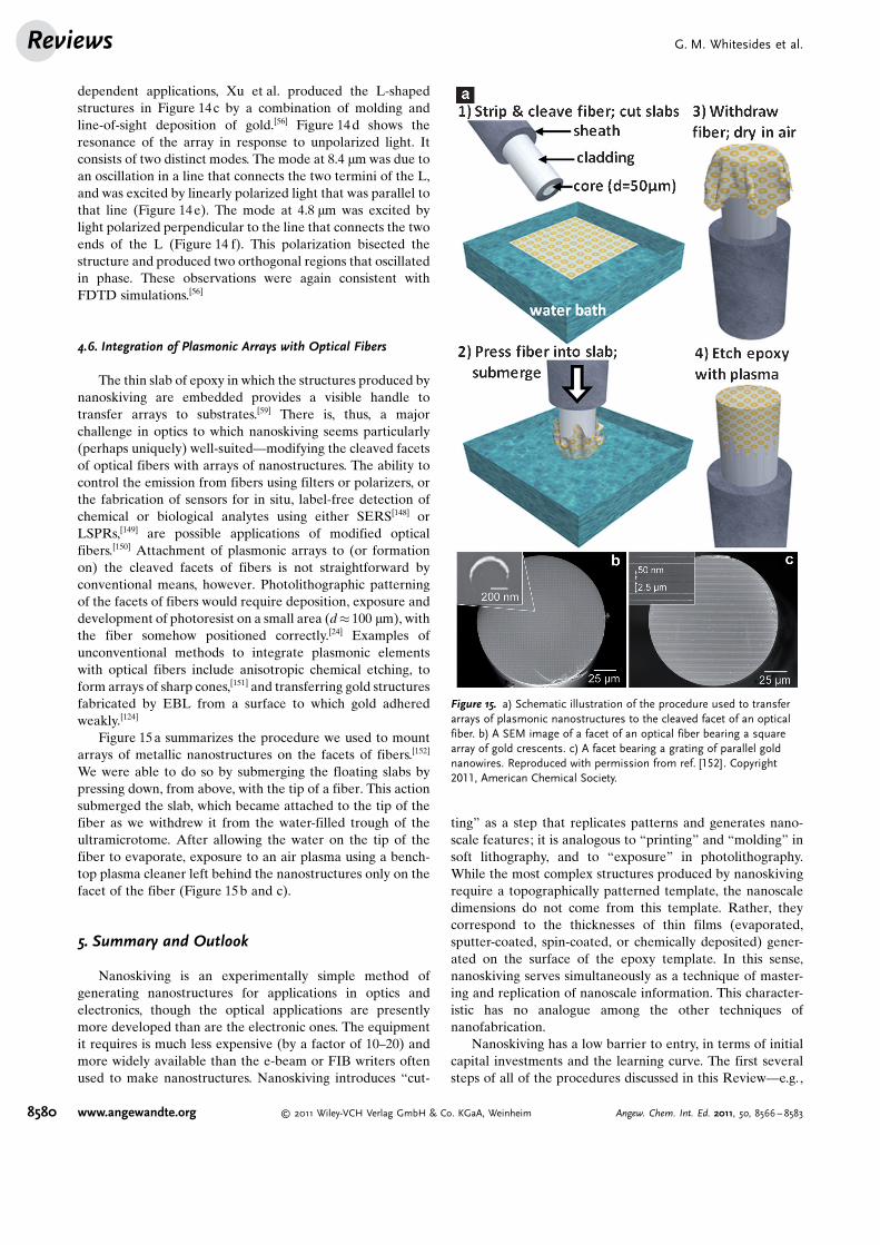
Figure 15 a summarizes the procedure we used to mountarrays of metallic nanostructures on the facets of fibers.[152]
We were able to do so by submerging the floating slabs bypressing down, from above, with the tip of a fiber. This actionsubmerged the slab, which became attached to the tip of thefiber as we withdrew it from the water-filled trough of theultramicrotome. After allowing the water on the tip of thefiber to evaporate, exposure to an air plasma using a bench-top plasma cleaner left behind the nanostructures only on thefacet of the fiber (Figure 15b and c).
5. Summary and Outlook
Nanoskiving is an experimentally simple method ofgenerating nanostructures for applications in optics andelectronics, though the optical applications are presentlymore developed than are the electronic ones. The equipmentit requires is much less expensive (by a factor of 10–20) andmore widely available than the e-beam or FIB writers oftenused to make nanostructures. Nanoskiving introduces “cut-
ting” as a step that replicates patterns and generates nano-scale features; it is analogous to “printing” and “molding” insoft lithography, and to “exposure” in photolithography.While the most complex structures produced by nanoskivingrequire a topographically patterned template, the nanoscaledimensions do not come from this template. Rather, theycorrespond to the thicknesses of thin films (evaporated,sputter-coated, spin-coated, or chemically deposited) gener-ated on the surface of the epoxy template. In this sense,nanoskiving serves simultaneously as a technique of master-ing and replication of nanoscale information. This character-istic has no analogue among the other techniques ofnanofabrication.
Nanoskiving has a low barrier to entry, in terms of initialcapital investments and the learning curve. The first severalsteps of all of the procedures discussed in this Review—e.g.,
Figure 15. a) Schematic illustration of the procedure used to transferarrays of plasmonic nanostructures to the cleaved facet of an opticalfiber. b) A SEM image of a facet of an optical fiber bearing a squarearray of gold crescents. c) A facet bearing a grating of parallel goldnanowires. Reproduced with permission from ref. [152]. Copyright2011, American Chemical Society.
G. M. Whitesides et al.Reviews
8580 www.angewandte.org � 2011 Wiley-VCH Verlag GmbH & Co. KGaA, Weinheim Angew. Chem. Int. Ed. 2011, 50, 8566 – 8583

soft lithographic molding and thin-film deposition—are wellestablished in the literature and widely practiced.[153] A usercan start generating high-quality nanostructures after a half-day session of training, and a few sessions of independentpractice. Additional experience increases the speed withwhich samples can be trimmed and sectioned, but the qualityof the nanostructures obtained depends most strongly on thepreparation of blocks—molding, deposition, embedding, andorienting—rather than on the process of sectioning itself.
As with any technique, nanoskiving has its disadvantages.It is limited to generating non-crossing line segments(although these structures can be produced by stackingslabs). The technique works best for polymers and metalssofter than platinum; extensive fragmentation of brittlematerials—hard metals, crystalline oxides, and some amor-phous semiconductors—limits its generality (though thenumber of materials for which nanoskiving does work islarge). Nanoskiving is subject to all of the artifacts ofultramicrotomy, the most important of which are scoringand compression. Scoring can be avoided by working in anenvironment uncontaminated with hard, microscopic parti-cles of dust. Compression causes two deleterious effects. First,it distorts square arrays of nanostructures into rectangulararrays (8.5% compression for UVO-114). Second, it imposescompressive stress on embedded films that lie parallel to thedirection of cutting, and these segments are prone tofragmentation. The use of oscillating knives and othermethods[64, 154] will mitigate these deleterious effects as nano-skiving develops.[155]
There are several future directions of nanoskiving. Inoptics, the two most salient are 1) the ability to fabricatestructures of multiple materials and 2) the integration ofarrays of metallic nanoparticles with optical fibers and othercomponents. The fabrication of three-dimensional metama-terials is also an area of potential significance for nano-skiving.[130,133] Stacking and laminating structures could be aroute toward 3D materials with different geometries andcompositions within or between layers.[59, 74] Other areas inwhich nanoskiving has potential are nanoelectrochemistry,[80]
patterning nanoscale magnetic particles for digital storage,[156]
membranes for size or shape-selective diffusion,[157] devicesfor energy conversion and storage,[158] and patterning func-tional surfaces for biology.[159]
The ability to produce consecutive cross sections—quasicopies—of structures suggests that thin sectioning could beuseful in manufacturing. The most significant impediment totransforming nanoskiving from a technique for research toone of manufacturing is replacing the manual steps (aligningthe embedded structures with the knife edge and collectingthe sections from the water-filled trough) with automatedones. A recent technological development—reel-to-reel lath-ing ultramicrotomy—stands out as potentially useful for high-throughput and large-area nanoskiving.[160] Nanoskivingmight, ultimately, suggest new ways of nanomanufacturingby cutting.
This research was supported by the National Science Founda-tion under award PHY-0646094 and by the Office of NavalResearch under award N0014-10-1-0942. The authors used the
shared facilities supported by the NSF under MRSEC (DMR-0213805 and DMR-0820484). This work was performed in partusing the facilities of the Center for Nanoscale Systems (CNS),a member of the National Nanotechnology InfrastructureNetwork (NNIN), which is supported by the National ScienceFoundation under NSF award no. ECS-0335765. CNS is part ofthe Faculty of Arts and Sciences at Harvard University. D.J.L.acknowledges a Graduate Fellowship from the AmericanChemical Society, Division of Organic Chemistry, sponsoredby Novartis.
Received: February 10, 2011Published online: July 13, 2011
[1] C. B. Murray, C. R. Kagan, M. G. Bawendi, Annu. Rev. Mater.Sci. 2000, 30, 545.
[2] P. Mulvaney, MRS Bull. 2001, 26, 1009.[3] P. Avouris, Phys. Today 2009, 62, 34.[4] G. M. Whitesides, D. J. Lipomi, Faraday Discuss. 2009, 143, 373.[5] R. F. Pease, S. Y. Chou, Proc. IEEE 2008, 96, 248.[6] B. Y. S. Kim, J. T. Rutka, W. C. W. Chan, N. Engl. J. Med. 2010,
363, 2434.[7] A. V. Akimov, A. Mukherjee, C. L. Yu, D. E. Chang, A. S.
Zibrov, P. R. Hemmer, H. Park, M. D. Lukin, Nature 2007, 450,402.
[8] E. Cubukcu, N. F. Yu, E. J. Smythe, L. Diehl, K. B. Crozier, F.Capasso, IEEE J. Sel. Top. Quantum Electron. 2008, 14, 1448.
[9] B. D. Gates, Q. B. Xu, M. Stewart, D. Ryan, C. G. Willson,G. M. Whitesides, Chem. Rev. 2005, 105, 1171.
[10] C. G. Willson, B. J. Roman, ACS Nano 2008, 2, 1323.[11] R. K. Cavin, V. V. Zhirnov, D. J. C. Herr, A. Avila, J. Hutchby, J.
Nanopart. Res. 2006, 8, 841.[12] M. Lundstrom, Science 2003, 299, 210.[13] M. Gower, Microlithogr. World 2004, 13, 16.[14] H. Ito, J. Photopolym. Sci. Technol. 2008, 21, 475.[15] J. L�pez-Gejo, J. T. Kunjappu, J. Zhou, B. W. Smith, P.
Zimmerman, W. Conley, N. J. Turro, Chem. Mater. 2007, 19,3641.
[16] K. Ronse, C. R. Phys. 2006, 7, 844.[17] C. A. Mack, IEEE Spectrum 2008, 45, 46.[18] D. Bratton, D. Yang, J. Y. Dai, C. K. Ober, Polym. Adv.
Technol. 2006, 17, 94.[19] C. N. Berglund, R. C. Leachman, IEEE Trans. Semicond.
Manuf. 2010, 23, 39.[20] C. G. Wilson, J. Photopolym. Sci. Technol. 2009, 22, 147.[21] B. J. Wiley, D. Qin, Y. N. Xia, ACS Nano 2010, 4, 3554.[22] Y. N. Xia, E. Kim, X. M. Zhao, J. A. Rogers, M. Prentiss, G. M.
Whitesides, Science 1996, 273, 347.[23] D. H. Kim, J. A. Rogers, Adv. Mater. 2008, 20, 4887.[24] E. J. Smythe, M. D. Dickey, G. M. Whitesides, F. Capasso, ACS
Nano 2009, 3, 59.[25] Y. N. Xia, G. M. Whitesides, Angew. Chem. 1998, 110, 568;
Angew. Chem. Int. Ed. 1998, 37, 550.[26] C. Goh, K. M. Coakley, M. D. McGehee, Nano Lett. 2005, 5,
1545.[27] Q. B. Xu, B. T. Mayers, M. Lahav, D. V. Vezenov, G. M.
Whitesides, J. Am. Chem. Soc. 2005, 127, 854.[28] Y. N. Xia, J. J. McClelland, R. Gupta, D. Qin, X. M. Zhao, L. L.
Sohn, R. J. Celotta, G. M. Whitesides, Adv. Mater. 1997, 9, 147.[29] E. Kim, Y. N. Xia, X. M. Zhao, G. M. Whitesides, Adv. Mater.
1997, 9, 651.[30] N. L. Jeon, I. S. Choi, B. Xu, G. M. Whitesides, Adv. Mater.
1999, 11, 946.[31] R. S. Kane, S. Takayama, E. Ostuni, D. E. Ingber, G. M.
Whitesides, Biomaterials 1999, 20, 2363.
Nanoskiving
8581Angew. Chem. Int. Ed. 2011, 50, 8566 – 8583 � 2011 Wiley-VCH Verlag GmbH & Co. KGaA, Weinheim www.angewandte.org

[32] Y. N. Xia, G. M. Whitesides, Langmuir 1997, 13, 2059.[33] H. A. Biebuyck, N. B. Larsen, E. Delamarche, B. Michel, IBM
J. Res. Dev. 1997, 41, 159.[34] Y. N. Xia, D. Qin, G. M. Whitesides, Adv. Mater. 1996, 8, 1015.[35] T. B. Cao, Q. B. Xu, A. Winkleman, G. M. Whitesides, Small
2005, 1, 1191.[36] M. Q. Xue, Y. H. Yang, T. B. Cao, Adv. Mater. 2008, 20, 596.[37] D. J. Shir, S. Jeon, H. Liao, M. Highland, D. G. Cahill, M. F. Su,
I. F. El-Kady, C. G. Christodoulou, G. R. Bogart, A. V. Hamza,J. A. Rogers, J. Phys. Chem. B 2007, 111, 12945.
[38] J. Maria, S. Jeon, J. A. Rogers, J. Photochem. Photobiol. A 2004,166, 149.
[39] J. A. Rogers, K. E. Paul, R. J. Jackman, G. M. Whitesides, Appl.Phys. Lett. 1997, 70, 2658.
[40] S. Y. Chou, P. R. Krauss, P. J. Renstrom, Appl. Phys. Lett. 1995,67, 3114.
[41] S. Y. Chou, P. R. Krauss, P. J. Renstrom, Science 1996, 272, 85.[42] T. C. Bailey, S. C. Johnson, S. V. Sreenivasan, J. G. Ekerdt, C. G.
Willson, D. J. Resnick, J. Photopolym. Sci. Technol. 2002, 15,481.
[43] R. Garcia, R. V. Martinez, J. Martinez, Chem. Soc. Rev. 2006,35, 29.
[44] W. Shim, A. B. Braunschweig, X. Liao, J. N. Chai, J. K. Lim,G. F. Zheng, C. A. Mirkin, Nature 2011, 469, 516.
[45] K. Salaita, Y. H. Wang, J. Fragala, R. A. Vega, C. Liu, C. A.Mirkin, Angew. Chem. 2006, 118, 7378; Angew. Chem. Int. Ed.2006, 45, 7220.
[46] L. G. Rosa, J. Liang, J. Phys. Condens. Matter 2009, 21, 483001.[47] J. L. Gong, D. J. Lipomi, J. D. Deng, Z. H. Nie, X. Chen, N. X.
Randall, R. Nair, G. M. Whitesides, Nano Lett. 2010, 10, 2702.[48] T. F. Malis, D. Steele, Mater. Res. Soc. Symp. Proc. 1990, 199, 3.[49] W. Villiger, A. Bremer, J. Struct. Biol. 1990, 104, 178.[50] Q. B. Xu, R. M. Rioux, M. D. Dickey, G. M. Whitesides, Acc.
Chem. Res. 2008, 41, 1566.[51] J. Hill, The Construction of Timber, Imperial Academy,
London, 1770.[52] D. C. Pease, K. R. Porter, J. Cell Biol. 1981, 91, 287s.[53] B. M. Bracegirdle, A History of Microtechnique, Cornell
University Press, Ithaca, 1978.[54] J. N. Goldstein, D. Newbury, D. Joy, C. Lyman, P. Echlin, E.
Lifshin, L. Sawyer, J. Michael, Scanning Electron Microscopyand X-Ray Analysis, 3rd ed., Springer, Berlin, 2003.
[55] J. D. Acetarin, E. Carlemalm, E. Kellenberger, W. Villiger, J.Electron Microsc. Tech. 1987, 6, 63.
[56] Q. B. Xu, J. M. Bao, R. M. Rioux, R. Perez-Castillejos, F.Capasso, G. M. Whitesides, Nano Lett. 2007, 7, 2800.
[57] D. J. Lipomi, R. V. Martinez, R. M. Rioux, L. Cademartiri,W. F. Reus, G. M. Whitesides, ACS Appl. Mater. Interfaces 2010,2, 2503.
[58] A. Antonovsky, Microsc. Res. Tech. 1995, 31, 300.[59] D. J. Lipomi, M. A. Kats, P. Kim, S. H. Kang, J. Aizenberg, F.
Capasso, G. M. Whitesides, ACS Nano 2010, 4, 4017.[60] Q. Xu, R. M. Rioux, G. M. Whitesides, ACS Nano 2007, 1, 215.[61] B. J. Wiley, D. J. Lipomi, J. M. Bao, F. Capasso, G. M. White-
sides, Nano Lett. 2008, 8, 3023.[62] D. J. Lipomi, R. C. Chiechi, W. F. Reus, G. M. Whitesides, Adv.
Funct. Mater. 2008, 18, 3469.[63] T. R. Matzelle, H. Gnaegi, A. Ricker, R. Reichelt, J. Microsc.
2003, 209, 113.[64] J. C. Jesior, J. Ultrastruct. Mol. Struct. Res. 1986, 95, 210.[65] Q. B. Xu, J. M. Bao, F. Capasso, G. M. Whitesides, Angew.
Chem. 2006, 118, 3713; Angew. Chem. Int. Ed. 2006, 45, 3631.[66] Y. Xia, Y. J. Xiong, B. Lim, S. E. Skrabalak, Angew. Chem.
2009, 121, 62; Angew. Chem. Int. Ed. 2009, 48, 60.[67] C. Burda, X. B. Chen, R. Narayanan, M. A. El-Sayed, Chem.
Rev. 2005, 105, 1025.[68] J. Robertson, Rep. Prog. Phys. 2006, 69, 327.
[69] A. K. Geim, K. S. Novoselov, Nat. Mater. 2007, 6, 183.[70] Y. N. Xia, P. D. Yang, Y. G. Sun, Y. Y. Wu, B. Mayers, B. Gates,
Y. D. Yin, F. Kim, Y. Q. Yan, Adv. Mater. 2003, 15, 353.[71] A. L. Falk, F. H. L. Koppens, C. L. Yu, K. Kang, N. D. Snapp,
A. V. Akimov, M. H. Jo, M. D. Lukin, H. Park, Nat. Phys. 2009,5, 475.
[72] Q. B. Xu, B. D. Gates, G. M. Whitesides, J. Am. Chem. Soc.2004, 126, 1332.
[73] M. D. Dickey, D. J. Lipomi, P. J. Bracher, G. M. Whitesides,Nano Lett. 2008, 8, 4568.
[74] D. J. Lipomi, F. Ilievski, B. J. Wiley, P. B. Deotare, M. LonÅar,G. M. Whitesides, ACS Nano 2009, 3, 3315.
[75] D. J. Lipomi, R. C. Chiechi, M. D. Dickey, G. M. Whitesides,Nano Lett. 2008, 8, 2100.
[76] K. Ramanathan, M. A. Bangar, M. H. Yun, W. F. Chen, A.Mulchandani, N. V. Myung, Nano Lett. 2004, 4, 1237.
[77] M. H. Yun, N. V. Myung, R. P. Vasquez, C. S. Lee, E. Menke,R. M. Penner, Nano Lett. 2004, 4, 419.
[78] A. Bezryadin, C. Dekker, G. Schmid, Appl. Phys. Lett. 1997, 71,1273.
[79] R. Holzel, N. Calander, Z. Chiragwandi, M. Willander, F. F.Bier, Phys. Rev. Lett. 2005, 95, 128102.
[80] R. W. Murray, Chem. Rev. 2008, 108, 2688.[81] N. J. Tao, Nat. Nanotechnol. 2006, 1, 173.[82] E. A. Weiss, J. K. Kriebel, M. A. Rampi, G. M. Whitesides,
Philos. Trans. R. Soc. London Ser. A 2007, 365, 1509.[83] J. B. Lassiter, J. Aizpurua, L. I. Hernandez, D. W. Brandl, I.
Romero, S. Lal, J. H. Hafner, P. Nordlander, N. J. Halas, NanoLett. 2008, 8, 1212.
[84] H. Q. Liu, J. Kameoka, D. A. Czaplewski, H. G. Craighead,Nano Lett. 2004, 4, 671.
[85] D. T. McQuade, A. E. Pullen, T. M. Swager, Chem. Rev. 2000,100, 2537.
[86] E. C. Walter, F. Favier, R. M. Penner, Anal. Chem. 2002, 74,1546.
[87] E. C. Walter, B. J. Murray, F. Favier, G. Kaltenpoth, M. Grunze,R. M. Penner, J. Phys. Chem. B 2002, 106, 11407.
[88] E. A. Weiss, G. K. Kaufman, J. K. Kriebel, Z. Li, R. Schalek,G. M. Whitesides, Langmuir 2007, 23, 9686.
[89] M. E. Roberts, A. N. Sokolov, Z. N. Bao, J. Mater. Chem. 2009,19, 3351.
[90] K. Ramanathan, M. A. Bangar, M. Yun, W. Chen, N. V. Myung,A. Mulchandani, J. Am. Chem. Soc. 2005, 127, 496.
[91] J. L. Duvail, P. Retho, V. Fernandez, G. Louarn, P. Molinie, O.Chauvet, J. Phys. Chem. B 2004, 108, 18552.
[92] H. Q. Liu, C. H. Reccius, H. G. Craighead, Appl. Phys. Lett.2005, 87, 253106.
[93] E. Smela, Adv. Mater. 2003, 15, 481.[94] S. Samitsu, T. Shimomura, K. Ito, M. Fujimori, S. Heike, T.
Hashizume, Appl. Phys. Lett. 2005, 86, 233103.[95] B. Dong, N. Lu, M. Zelsmann, N. Kehagias, H. Fuchs, C. M. S.
Torres, L. F. Chi, Adv. Funct. Mater. 2006, 16, 1937.[96] A. Greiner, J. H. Wendorff, Angew. Chem. 2007, 119, 5770;
Angew. Chem. Int. Ed. 2007, 46, 5670.[97] J. Kameoka, D. Czaplewski, H. Q. Liu, H. G. Craighead, J.
Mater. Chem. 2004, 14, 1503.[98] See Ref. [84].[99] G. Li, V. Shrotriya, J. S. Huang, Y. Yao, T. Moriarty, K. Emery,
Y. Yang, Nat. Mater. 2005, 4, 864.[100] J. T. McCann, J. I. L. Chen, D. Li, Z. G. Ye, Y. N. Xia, Chem.
Phys. Lett. 2006, 424, 162.[101] C. A. Stover, D. L. Koch, C. Cohen, J. Fluid Mech. 1992, 238,
277.[102] Z. H. Zhong, D. L. Wang, Y. Cui, M. W. Bockrath, C. M.
Lieber, Science 2003, 302, 1377.[103] Y. Cui, C. M. Lieber, Science 2001, 291, 851.
G. M. Whitesides et al.Reviews
8582 www.angewandte.org � 2011 Wiley-VCH Verlag GmbH & Co. KGaA, Weinheim Angew. Chem. Int. Ed. 2011, 50, 8566 – 8583
[104] Y. Huang, X. F. Duan, Q. Q. Wei, C. M. Lieber, Science 2001,291, 630.
[105] B. Messer, J. H. Song, P. D. Yang, J. Am. Chem. Soc. 2000, 122,10232.
[106] G. H. Yu, A. Y. Cao, C. M. Lieber, Nat. Nanotechnol. 2007, 2,372.
[107] Z. Y. Fan, J. C. Ho, Z. A. Jacobson, R. Yerushalmi, R. L. Alley,H. Razavi, A. Javey, Nano Lett. 2008, 8, 20.
[108] S. Jin, D. M. Whang, M. C. McAlpine, R. S. Friedman, Y. Wu,C. M. Lieber, Nano Lett. 2004, 4, 915.
[109] P. J. Pauzauskie, A. Radenovic, E. Trepagnier, H. Shroff, P. D.Yang, J. Liphardt, Nat. Mater. 2006, 5, 97.
[110] A. Jamshidi, P. J. Pauzauskie, P. J. Schuck, A. T. Ohta, P. Y.Chiou, J. Chou, P. D. Yang, M. C. Wu, Nat. Photonics 2008, 2,86.
[111] H. W. C. Postma, A. Sellmeijer, C. Dekker, Adv. Mater. 2000,12, 1299.
[112] D. J. Sirbuly, M. Law, P. Pauzauskie, H. Q. Yan, A. V. Maslov,K. Knutsen, C. Z. Ning, R. J. Saykally, P. D. Yang, Proc. Natl.Acad. Sci. USA 2005, 102, 7800.
[113] P. A. Smith, C. D. Nordquist, T. N. Jackson, T. S. Mayer, B. R.Martin, J. Mbindyo, T. E. Mallouk, Appl. Phys. Lett. 2000, 77,1399.
[114] M. Q. Xue, Y. Zhang, Y. L. Yang, T. B. Cao, Adv. Mater. 2008,20, 2145.
[115] R. D. McCullough, Adv. Mater. 1998, 10, 93.[116] B. C. Thompson, J. M. J. Fr�chet, Angew. Chem. 2008, 120, 62;
Angew. Chem. Int. Ed. 2008, 47, 58.[117] K. M. Coakley, M. D. McGehee, Chem. Mater. 2004, 16, 4533.[118] S. A. Maier, H. A. Atwater, J. Appl. Phys. 2005, 98, 011101.[119] M. E. Stewart, C. R. Anderton, L. B. Thompson, J. Maria, S. K.
Gray, J. A. Rogers, R. G. Nuzzo, Chem. Rev. 2008, 108, 494.[120] J. C. Love, K. E. Paul, G. M. Whitesides, Adv. Mater. 2001, 13,
604.[121] D. M. Wu, N. Fang, C. Sun, X. Zhang, W. J. Padilla, D. N. Basov,
D. R. Smith, S. Schultz, Appl. Phys. Lett. 2003, 83, 201.[122] A. K. Sharma, R. Jha, B. D. Gupta, IEEE Sens. J. 2007, 7, 1118.[123] K. Kneipp, H. Kneipp, I. Itzkan, R. R. Dasari, M. S. Feld, J.
Phys. Condens. Matter 2002, 14, R597.[124] E. J. Smythe, M. D. Dickey, J. M. Bao, G. M. Whitesides, F.
Capasso, Nano Lett. 2009, 9, 1132.[125] X. F. Liu, C. H. Sun, N. C. Linn, B. Jiang, P. Jiang, J. Phys.
Chem. C 2009, 113, 14804.[126] E. Fort, S. Gresillon, J. Phys. D 2008, 41, 013001.[127] P. Peumans, V. Bulovic, S. R. Forrest, Appl. Phys. Lett. 2000, 76,
2650.[128] T. A. Klar, A. V. Kildishev, V. P. Drachev, V. M. Shalaev, IEEE
J. Sel. Top. Quantum Electron. 2006, 12, 1106.[129] J. B. Pendry, A. J. Holden, D. J. Robbins, W. J. Stewart, IEEE
Trans. Microwave Theory Tech. 1999, 47, 2075.[130] J. Valentine, S. Zhang, T. Zentgraf, E. Ulin-Avila, D. A. Genov,
G. Bartal, X. Zhang, Nature 2008, 455, 376.[131] J. B. Pendry, Phys. Rev. Lett. 2000, 85, 3966.[132] J. B. Pendry, D. Schurig, D. R. Smith, Science 2006, 312, 1780.
[133] N. Liu, H. C. Guo, L. W. Fu, S. Kaiser, H. Schweizer, H.Giessen, Nat. Mater. 2008, 7, 31.
[134] J. K. Gansel, M. Thiel, M. S. Rill, M. Decker, K. Bade, V. Saile,G. von Freymann, S. Linden, M. Wegener, Science 2009, 325,1513.
[135] A. Ahmadi, S. Ghadarghadr, H. Mosallaei, Opt. Express 2010,18, 123.
[136] C. L. Haynes, R. P. Van Duyne, J. Phys. Chem. B 2001, 105,5599.
[137] M. C. Gwinner, E. Koroknay, L. W. Fu, P. Patoka, W. Kandul-ski, M. Giersig, H. Giessen, Small 2009, 5, 400.
[138] K. E. Paul, C. Zhu, J. C. Love, G. M. Whitesides, Appl. Opt.2001, 40, 4557.
[139] M. E. Stewart, N. H. Mack, V. Malyarchuk, J. Soares, T. W. Lee,S. K. Gray, R. G. Nuzzo, J. A. Rogers, Proc. Natl. Acad. Sci.USA 2006, 103, 17143.
[140] J. Henzie, J. E. Barton, C. L. Stender, T. W. Odom, Acc. Chem.Res. 2006, 39, 249.
[141] J. Lee, W. Hasan, C. L. Stender, T. W. Odom, Acc. Chem. Res.2008, 41, 1762.
[142] A. L. Pyayt, B. J. Wiley, Y. N. Xia, A. Chen, L. Dalton, Nat.Nanotechnol. 2008, 3, 660.
[143] P. Nagpal, N. C. Lindquist, S. H. Oh, D. J. Norris, Science 2009,325, 594.
[144] H. Ditlbacher, A. Hohenau, D. Wagner, U. Kreibig, M. Rogers,F. Hofer, F. R. Aussenegg, J. R. Krenn, Phys. Rev. Lett. 2005, 95,257403.
[145] M. Allione, V. V. Temnov, Y. Fedutik, U. Woggon, M. V.Artemyev, Nano Lett. 2008, 8, 31.
[146] A. Graff, D. Wagner, H. Ditlbacher, U. Kreibig, Eur. Phys. J. D2005, 34, 263.
[147] C. X. Kan, X. G. Zhu, G. H. Wang, J. Phys. Chem. B 2006, 110,4651.
[148] A. Lucotti, G. Zerbi, Sens. Actuators B 2007, 121, 356.[149] A. K. Sharma, R. Jha, B. D. Gupta, IEEE Sens. J. 2007, 7, 1118.[150] A. Leung, P. M. Shankar, R. Mutharasan, Sens. Actuators B
2007, 125, 688.[151] V. Guieu, D. Talaga, L. Servant, N. Sojic, F. Lagugne-Labarthet,
J. Phys. Chem. C 2009, 113, 874.[152] D. J. Lipomi, R. V. Martinez, M. A. Kats, S. H. Kang, P. Kim, J.
Aizenberg, F. Capasso, G. M. Whitesides, Nano Lett. 2011, 11,632 – 636.
[153] D. Qin, Y. N. Xia, G. M. Whitesides, Nat. Protoc. 2010, 5, 491.[154] J. C. Jesior, J. Ultrastruct. Res. 1985, 90, 135.[155] D. Studer, H. Gnaegi, J. Microsc. 2000, 197, 94.[156] J. Shi, S. Gider, K. Babcock, D. D. Awschalom, Science 1996,
271, 937.[157] N. B. McKeown, P. M. Budd, Chem. Soc. Rev. 2006, 35, 675.[158] K. Shah, W. C. Shin, R. S. Besser, Sens. Actuators B 2004, 97,
157.[159] D. B. Weibel, W. R. DiLuzio, G. M. Whitesides, Nat. Rev.
Microbiol. 2007, 5, 209.[160] N. Kasthuri, K. Hayworth, J. C. Tapia, R. Schalek, S. Nundy,
J. W. Lichtman, Soc. Neurosci. Abstr. 2009.
Nanoskiving
8583Angew. Chem. Int. Ed. 2011, 50, 8566 – 8583 � 2011 Wiley-VCH Verlag GmbH & Co. KGaA, Weinheim www.angewandte.org