data communication systems - diploma
TRANSCRIPT

- 1 -
S.Y. Diploma : Sem. IV [ET/EN/EX/EJ]
Data Communication Systems Time: 3 Hrs.] Prelim Question Paper Solution [Marks : 70
Q.1 Attempt any FIVE of the following : [10]Q.1(a) Define entropy and state its unit. [2]Ans.: Entropy is defined as the average number of bits per symbol needed to encode long
sequences of symbols emitted by the source. Its unit is bits/symbol Mathematically
H = M
i 2i 1 i
1P logP=
Where H is entropy, pi is the probabilities of the occurrence of the ith symbol Q.1(b) State Shannon Hartley theorem. [2]Ans.: Shannon’s Hartely theorem
Statement: The channel capacity of a white, band limited Gaussian channel is given by,
C = Blog2
+
S1 bitssec.N
Where B = Channel Bandwidth S = Signal Power N = Noise within the channel bandwidth.
Q.1(c) State sampling theorem. [2]Ans.: Sampling Theorem Sampling theorem states that any band limit signal with maximum frequency ‘Fm’ can be fully
reconstructed from it’s sampled version provided that the sampling frequency ‘Fs’ should be greater than or equal to twice the ‘Fm’ i.e. Fs ≥ 2 Fm, where Fs is known as sampling frequency or sampling rate. This rate of sampling frequency is also known as “Nyquist Rate”.
Q.1(d) State the need of multiplexing and write it’s type. [2]Ans.: Need of multiplexing in the application like telephony there are large numbers of users
involved. It is not possible to lay a separate pair of wires from each subscriber to the other entire subscriber; this is very expensive and practically impossible.
In the Process of multiplexing two or more individual signals are transmitted over a single communication channel. Here we used medium as a coaxial cable or an optical fiber cable because of multiplexing bandwidth utilization is possible. As the data and telecommunications usage increases, so does the traffic. We can accommodate this increase by continuing to add individual lines each time a new channel is needed, or we can install higher capacity links and use each to carry multiple signals. Today’s technology includes high-bandwidth transmission media such as coaxial cable, optical fiber and terrestrial and satellite microwaves. Each of these has a carrying capacity (bandwidth) far in excess of that needed for the average transmission signal. If the bandwidth of the link is greater than the transmission needs of the devices connected to it, the excess capacity is wasted. An efficient system maximizes the utilization of all resources. Bandwidth is one of the most precious resources in data communications.
Vidyalankar : S.Y. Diploma − DC
- 2 -
Types of multiplexing: 1. Analog multiplexing: Frequency division multiplexing
Wavelength division multiplexing
2. Digital multiplexing: Time division multiplexing Code division multiplexing
Q.1(e) State advantages of digital communication system. [2]Ans.: Advantages of Digital Communications system
(i) Because of the advances of IC technologies and high speed computers, digital communication systems are simpler and cheaper compared to analog systems.
(ii) Using data encryption, only permitted receivers can be allowed to detect the transmitted data. This is very useful in military applications.
(iii) This wide dynamic range is possible since the data is converted to the digital form. (iv) Using multiplexing, the speech, video and other data can be merged and transmitted over
common channel. Q.1(f) List the applications of spread spectrum modulation. [2]Ans.: 1. Military application- resistance to gainming. 2. Secure communication. 3. CDMA in satellite communication. 4. Police radar can employ spread spectrum to avoid detection by detectors employed by
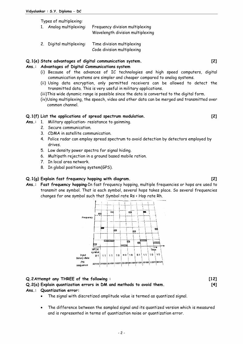
drives. 5. Low density power spectra for signal hiding. 6. Multipath rejection in a ground based mobile ration. 7. In local area network. 8. In global positioning system(GPS). Q.1(g) Explain fast frequency hopping with diagram. [2]Ans.: Fast frequency hopping-In fast frequency hopping, multiple frequencies or hops are used to
transmit one symbol. That is each symbol, several hops takes place. So several frequencies changes for one symbol such that Symbol rate Rs < Hop rate Rh.
Q.2 Attempt any THREE of the following : [12]Q.2(a) Explain quantization errors in DM and methods to avoid them. [4]Ans.: Quantization error:
• The signal with discretized amplitude value is termed as quantized signal. • The difference between the sampled signal and its quantized version which is measured
and is represented in terms of quantization noise or quantization error.
Prelim Question Paper Solution
- 3 -
Quantization process: • Quantization is the process of approximation or rounding off the sampled signal. The
quantizer converts sampled signal into approximated rounded values consisting of only finite no. of pre decided voltage levels called as quantization levels.
• In the process of A to D conversion, after sampling, quantization is the next step. The input signal x(t) is assumed to have a peak swing of VL to VH volts. This entire voltage range has been divided into Q equal intervals each of size “s”. s is called as step size and its value is given as S= VH-VL / Q
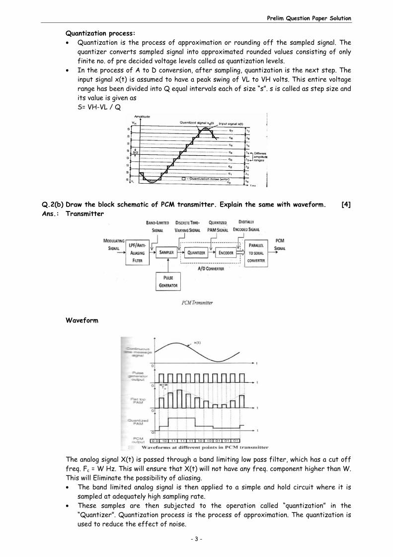
Q.2(b) Draw the block schematic of PCM transmitter. Explain the same with waveform. [4]Ans.: Transmitter
Waveform
The analog signal X(t) is passed through a band limiting low pass filter, which has a cut off freq. Fc = W Hz. This will ensure that X(t) will not have any freq. component higher than W. This will Eliminate the possibility of aliasing.
• The band limited analog signal is then applied to a simple and hold circuit where it is sampled at adequately high sampling rate.
• These samples are then subjected to the operation called “quantization” in the “Quantizer”. Quantization process is the process of approximation. The quantization is used to reduce the effect of noise.

Vidyalankar : S.Y. Diploma − DC
- 4 -
• The quantized Pam pulses are applied to an encoder which basically an A to D convertor. Each quantized level is converted into an N bit digital word by the A to D convertor.
• The encoder output is converted into a stream of pulses by the parallel to serial converter block. Thus at the PCM transmitter output we get a train of digital pulses.
Q.2(c) Encode the following Binary data stream into unipolar RZ, unipolar NRZ, AMI and
split phase Manchester code Data stream : 10110100101. [4]
Ans.:
Q.2(d) Draw the DPSK transmitter and outline its working principle. [4]Ans.: [Explanation- 2 marks, Diagram- 2 marks]
Principle It combines, differential encoding and phase shift keying. In BPSK receiver, the carrier recovery is done by squaring the received signal.
Hence, when the received signal is generated by negative data bit, it is squared and thus we cannot determine if the received bit is -b(t) or b(t.) Hence DPSK is used to eliminate the ambiguity of the received bit.
Operation 1) d (t) represents the data stream which is to be transmitted it is to one input of an EX-
OR logic gate. 2) The EX-OR gate output "b (t)" is delayed by one bit period the applied to the other
input of EX-OR gate. 3) The delayed represented by "b (t-Tb)". Depending on the values of "d (t)" and "b (t-Tb)"
the EX-OR produces the output sequence "b (t)".The waveform for the generator .the waveform drawn by arbitrarily assuming that in the first interval b (0) = 0
Bipolar NRZ level shifter
Balanced modulator
DPSK output
Carrier oscillator
b′(t)b(t)
b(t − TD)
+
Delay TD
Data stream
x(t)
S2P cos ωCt

Prelim Question Paper Solution
- 5 -
4) Output of EX-OR gate is the applied to a bipolar NRZ level which converts "b (t)" to a bipolar level "b(t) as shown
b(t) b'(t) 0 -1 1 +1 VDpsk(t)= √(2Ps) cos ωt That Means no phase Shift has been introduced But when b (t) = 0, b (t) = -1 Hence VDpsk (t)= -√ (2Ps) cos ωt Thus 180° Phase shift is introduced to represent b (t) =0
Q.3 Attempt any THREE of the following : [12]Q.3(a) With the help of neat sketch explain quantization process. [4]Ans.: Quantization In PCM process after sampling we perform quantization.
As shown in the block diagram, at the output of sampler, we get samples of random values but the encoder or ADC requires samples of fix and definite values. Hence to convert random value samples into fix value we make use of quantizer. For example the first sample is of value 1.2 V. But ADC requires 1V, hence quantizer converts 1.2 V sample into 1V; and gives it to the ADC. Similarly the 2nd sample is having value 4.6 V, then quiantizer will quantize it into nearest standard value of 5V and so on. The following figure explains the quantization process.
Let m(t) is a signal which is to be quantized. The signal m(t) varies from VL to VH, where VL = lowest value of signal VH = Highest value of signal
We divide the overall signal into M equal intervals, each interval is known as step size and it is given as
Step size (S) = −H LV VM
In the center of each step, we locate quantization levels m0, m1, m2, etc. The quantization takes place as follows :
During the given sampling interval first we check signal m(t) lies in which range. If signal lies in range Δ0, then quantizer converts it into level m0. If signal lies in the range Δ1, then
Amplitude
VH
S/
VL s
s
s
s
s
s
s
s m7
m6
m5
m4
m3
m2
m1
m0
Δ7
Δ6
Δ5
Δ4
Δ3
Δ2
Δ1
Δ0 Quantization Noise (error)
Quantized signal, mq(t) Input signal, m(t)
Different amplitude ranges
Sampler Quantizer ADC
I/P Signal
Sampling Pulses
1V3V
5V
1.2V 3.4
4.6

Vidyalankar : S.Y. Diploma − DC
- 6 -
quantizer quantize it to the level m1. It means if sample is having value 1.2V, then quantizer quantize or rounds off to value 1V. Similarly if sample is having value 6.8 V, then quantizer round off to the nearest standard value 7V.
Q.3(b) Generate CRC code for data 1101010011 when the dinsor is 01011 [4]Ans.: [Note - The divisor given is 01011, it should be taken as 1011 else it won't be solved] To generate the CRC code as divisor is 4 bit, add three zeros to the data and get the
remainder as shown below. The last three bit remainder is the required CRC send along with the data to be transmitted.
The CRC Data is 111. The final coded data transmitted will be
Q.3(c) Draw block diagram of DPCM transmitter and receiver. [4]Ans.: Differential Pulse Code Modulation (DPCM) In PCM we always sample the signal to a rate which is
slightly greater than Nyquist Rate, because of which we get large numbers of samples. Due to this two successive samples are highly correlated with each other, therefore it may happens that for two or three consecutive cycle we may transmit same binary code. This is known as “Reduandancy”.
As shown in the figure for sample 3TS, 4TS and 5TS we transmit the same binary code 110. The problem of redundancy can be avoided by encoding difference between the sample, rather than sample values. Thus in DPCM we take the difference between the two consecutive samples and then we encode this difference value. Since difference between samples are expected to be smaller than actual sample amplitude, therefore less number of bits are required for representing DPCM signal. DPCM Tx
000001010011100101110111
Ts 2Ts3Ts 4Ts 5Ts 6Ts
110
100 100101 101
010
Quantizer
Encoder
Predictor
DPCM output m(t)
m̂(t)
1 1 0 1 0 1 0 1 1 1 1 1
1 0 1 1 1 1 0 1 0 1 0 1 1 0 0 0
-1 01 1 1 1 0 0 - 1 01 1
1 1 1 1- 1 0 1 1
1 0 0 0- 1 0 1 1
0 1 1 1 1- 1 0 1 1
1 0 0 0- 1 0 1
1
0 1 1 0 0- 1 0 1 1
1 1 1
1 1 1 1 0 1 1 0 1
Prelim Question Paper Solution
- 7 -
The DPCM Tx works on the principle of prediction, the prediction may not be exact but it is close to the actual sample value. As shown in the figure m(t) is input or present sample and m̂(t) is a previous or predicated sample value. In DPCM we take the difference between present m(t) and previous m̂(t) sample value. This difference is known as error and denoted as e(t). ∴ e(t) = m(t) − m̂(t) The quantizer then quantizes error signal and transmits it via encoder. The function of prediction filter is to produce predicted value and it does by adding quantizer output with previous predicted value. This makes the prediction more and more close to the actual sample signal. DPCM Rx
In DPCM receiver the incoming binary signal is recovered using regenerator and decoded it to reconstruct the quantized difference signal. The prediction filter output and quantized difference signal are summed up to give quantize version of the original signal. This quantized signal is then pass through reconstruction filter to adverse original analog signal.
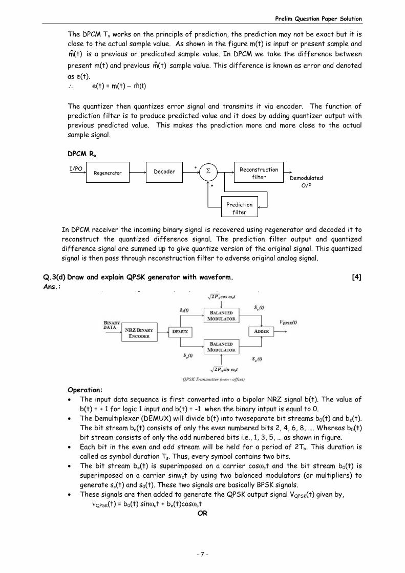
Q.3(d) Draw and explain QPSK generator with waveform. [4]Ans.:
Operation: • The input data sequence is first converted into a bipolar NRZ signal b(t). The value of
b(t) = + 1 for logic 1 input and b(t) = -1 when the binary intput is equal to 0. • The Demultiplexer (DEMUX) will divide b(t) into twoseparate bit streams b0(t) and be(t).
The bit stream be(t) consists of only the even numbered bits 2, 4, 6, 8, …. Whereas b0(t) bit stream consists of only the odd numbered bits i.e., 1, 3, 5, … as shown in figure.
• Each bit in the even and odd stream will be held for a period of 2Tb. This duration is called as symbol duration Ts. Thus, every symbol contains two bits.
• The bit stream be(t) is superimposed on a carrier cosωct and the bit stream b0(t) is superimposed on a carrier sinwct by using two balanced modulators (or multipliers) to generate sc(t) and s0(t). These two signals are basically BPSK signals.
• These signals are then added to generate the QPSK output signal VQPSK(t) given by, νQPSK(t) = b0(t) sinωct + be(t)cosωct
OR
Reconstruction filter
Decoder
Prediction filter
Regenerator
I/PO Demodulated
O/P
+
+

Vidyalankar : S.Y. Diploma − DC
- 8 -
The block diagram of offset QPSK transmitter is shwon in figure • In QPSK the transition for odd and even bit streams occur simultaneously. This leads to
sudden phase changes of the carrier 90° or 180° depnding upon whether the sign change occurs for only for one of the two components or both.
• Such sudden phase changes in the carrier can result in reduction of the amplitude of the QPSK signal when it is filtered. So if the QPSK signal during the course of transition is passed through a filter before the signal is detected, the resulting amplitude reduction of the signal can lead to errors in detection. Carrier phase changes by 180 in particular, cause considereble reduction in the envelope amplitude and so are to be avoided.
• As shown in the figure the even bit will occur before the 1st odd bit. Therefore, the odd bit stream b0(t) will start with a delay of one bit period Tb. This delay is called as Offset and therefore, this system is called as Offset QPSK. Because of this offset, the bit streams b0(t) and be(t) cannot change their levels at the same instant of time. Only one component can make transition at one time, changes are limited to 0°, 90°. Hence 180° phase shift is been avoided
• Here, the odd bit stream b0(t) has been delayed by one bit period Tb by adding a delay block as shown in figure.
As a result of this additional time delay, two bits which occur in time sequence (serially) in the input bit stream b(t), will appear at the same time (in parallel). Therefore, b0(t) and be(t) can change at different time after each time 2Tb and there can be a phase change in the output signal.

Prelim Question Paper Solution
- 9 -
Q.4 Attempt any THREE of the following : [12]Q.4(a) Explain hamming code for 1 bit error detection with example for data 1101. [4]Ans.: 1101 → Data Hamming code
1 1 0 P4 1 P2 P1 P1 = bit 3, 5, 7 1 0 1 P1 = 1
P2 = bit 2, 3, 6, 7 3, 6, 7 1 1 1 P2 = 0
P3 = bit 4, 5, 6, 7 5, 6, 7 1 0 1 P3 = 1 ∴ Code word
1 1 0 1 1 0 1 Q.4(b) Draw neat diagram of CCITT digital multiplexing hierarchy and explain in brief. [4]Ans.:
The diagram show 30 PCM Channels for CCITT digital hierarchy. • At E1, for 30 channels each have 64 Hbps. ∴ E1, 2.048 mbps Channel.
• At E2, for 4 channel each have 2.048 mbps ∴ E2, 8.448 mbps Channel.
• At E3, for 4 channel each have 8.448 mbps ∴ E3, 34.368 mbps.
• At E4, for 4 channels each have 34.368 mbps ∴ E4, 139.264 mbps
Q.4(c) Compare ASK & FSK [4]Ans.:
Parameters ASK FSK Variable characteristics Amplitude Frequency Bandwidth (Hz) Fb |f1 – f0 | + fb Noise immunity Low High Error probability High Low Performance in presence of noise
Poor Better than ASK
Complexity Simple Moderately complex Bit rate Suitable up to 100 its/sec Suitable up to about 1200 bits/sec Detection method Envelope Envelope
Mux
Mux
Mux
Mux
E1 or CEPT1 (2.048 Mbps)
8.448 Mbps
34.368 Mbps
139.264 Mbps
1
30 1
4
1
1
4

Vidyalankar : S.Y. Diploma − DC
- 10 -
Q.4(d) Describe the generation of BFSK with block diagram. [4]Ans.:
• In FSK, the frequency of the carrier is changed with respect to the input bits 1 & 0. • In case of binary data, two carrier frequencies are used. The carrier frequency
corresponding to logic 0 or binary 0 is called as space frequency and the carrier frequency corresponding to binary
1 is called as mark frequency. • As shown in Figure, the input binary data is given directly to the multiplier and is
inverted and given to second multiplier. • Two different carriers have different frequency generated by the two oscillators and
applied to the multipliers. • The output of both the multipliers is an ASK signal which is added by the summer. Thus,
the output of the adder is the BFSK wave. Q.4(e) Draw block diagram of QAM generation system and explain it with waveform. [4]Ans.:
Figures shows trensmitter for 4 bit QAM system. The input bit stream is applied to a serial
to parallel converter. Four seccessive bits are applied to the digital to analog converter. These bits are applied after every Ts second. Ts is the symbol period & Ts = 4Tb. Bits Bk & Bk + 1 are applied to upper digital to analog converter & Bk + 2, Bk + 3 are applied to lower D to A converter. Depending upon the two input bits, the output of D to A converter takes four output levels. Thus Ae (t) & Ao (t) takes 4 levels depending upon the combinaton of two input bits. As (t) modulates the carrier √Ps cos (2πf0t) and Ao (t) modulates √Ps sin (2πf0t).
The adder combines two signals to give QAM signal. It is given as, S (t) = Ae (t) √Ps cos (2πf0t) + Ao (t) √Ps sin (2πf0t).

Prelim Question Paper Solution
- 11 -
Waveforms-
Q.5 Attempt any TWO of the following : [12]Q.5(a) The probabilities of five source messages are m1 = 0.2, m2 = 0.3, m3 = 0.2,
m4 = 0.15 and m5 = 0.15. (i) Generate Huffman codes for the given source. (ii) Find the coding efficiency for Huffman coding.
[6]
Ans.: Message Stage I
m1 0.2 0.3 0.5 0.50 m2 0.3 0.2 0.3 0.51 m3 0.2 0.3 0.2 m4 0.15 0.2 m5 0.15
Codeword m1 m2 m3 m4 m5
0.2 0.3 0.2 0.15 0.15 01 10 11 000 001
Length = L L = (0.2 × 2) × 2 + (0.2 × 2) + (0.15 × 3) × 2 L = 0.8 + 0.6 + 0.9 L = 2.5 bits / symbol Q.5(b) Interpret the steps to convert digital signal into analog signal using QPSK
modulation with suitable block diagram. [6]
Ans.: • QPSK (Quadrature PSK) is an example of such multilevel phase modulation. • In QPSK system two successive bits in a bit stream are grouped together to form a
message and each message is represented by a distinct value of phase shift of the carrier.
0
1
0
1
0
1
Grouping of bits in QPSK

Vidyalankar : S.Y. Diploma − DC
- 12 -
Phase shift in QPSK
Symbol Phase 00(s1) 0 01(s2) 90 10(s3) 180 11(s4) 270
• Each symbol or message contains two bits. So the symbol duration Ts = 2Tb. • These symbols are transmitted by transmitting the same carrier frequency at four
different phase shifts as shown in Table and Fig. Since there are four phase shifts involved, this system is called as quadrature PSK or 4−PSK system.
• If the symbol 00 is to be transmitted then we have to transmit a carrier at 0° phase shift. If 01 is to be transmitted, then the same carrier is transmitted with a phase shift of 90°.
• Similarly the message 10 and 11 are transmitted by transmitting the carrier at 180° and 270° respectively.
• This concept will be clear after referring to the QPSK waveform of figure.
Q.5(c) Draw the circuit diagram of PN sequence generator for generating PN sequences
of length 15. Assuming initial contents of the shift register, to be all ones, explain its working. Generate the output sequence.
[6]
Ans.: Pseudo noise frequency sequence : The P-N sequence is actually a binary number which repeats after long number of pulses.
Hence it is known as pseudorandom sequence. This binary signal works like a high frequency noise signal and it is generated with the help of shift registers and combinational logic. The figure shows block diagram of P-N sequence generator. It consists of ‘x’ number of flipflops working as a shift registers. All the flipflops are clocked simultaneously and output of flipflop are given to a combinational circuit known as parity generator. The output of combinational circuit is against given back as input to 1 of flipflop and the P-N sequence is available from the output of last flip flop. For every clock pulse the state of previous flip flop is copied into the next flilp flop and thus at every clock pulse, a P-N sequence is shifted out from the last flip flop.
•
••
•
10(s3)90°
01(s2)
11(s4)
00(s1)
Constellation diagram of QPSK
Combinational logic or parity generator
F/F 1
F/F2
F/Fn
O/P

Prelim Question Paper Solution
- 13 -
In case of P-N sequence generator, the state 000 is not allowed, because once the shift register enters into the zero state then it will not come out it and overall P-N sequence will become 0. Hence, it is not allowed. Thus, if there are ‘n’ number of flipflop, then total number of states available are 2n − 1. It means the P-N sequence at the output will have period of 2n − 1 bits. The sequence of 2n − 1 length is known as “maximum length sequence”.
Properties of P-N sequence or maximum length sequence. The following are different properties of P-N sequence: (i) Balance property: This property states that in each period of maximum length
sequence, the number of 1’s is always one more than number of 0’s. This is known as balance property.
(ii) Run property: This property states that among the runs of 1’s and 0’s in each period of maximum length sequence, 1/2 runs of a each kind are of length one, 1/4th are of length 2, 1/8th are of length 3 and so on.
(iii) Co-relation property: This property checks that the auto co-relation of maximum length sequence is periodic and binary value.
Q.6 Attempt any TWO of the following : [12]Q.6(a) Describe DS-SS technique with block diagram in detail. [6]Ans.:
The modulated signal at the output of product modulator or multiplier i.e. s (t) is used
modulate tl carrier for BPSK modulation. The transmitted signal x(t) is thus DSSS signal. Product modulator output = s (t) S(t) = d(t)* c(t) The BPSK carrier signal is given by √2Ps sin 2πfC t. The output of BPSK modluator x(t) is transmitted x(t) = s(t) * √ 2Ps 2πfCt. But m (t) = ± 1 Therefore x(t) = ± √2Ps sin2πfC t. The phase shift of x(t) of x(t) is 0° to + m(t) at is 180° corresponding to a negiative m(t). At the receiver, the signal is coherently demodulated by multiplying the received signal by a
replica of the carrier. The signal r(t) at the input of the detector LPF is given by, r(t) = d(t)c(t) cosωct (2cosωct) = d(t)c(t) + m(t)c(t) cos 2ωct The LPF eliminates the high frequency components at 2ωc and retains only the low frequency
component y(t) = d(t)c(t).

Vidyalankar : S.Y. Diploma − DC
- 14 -
This component is then multiplied by the local code c(t) in phase with the receied code. C2(t) = 1.
At the output of the multiplier, this gives, z(t) = d(t)c(t)c(t) = d(t)
OR Direct sequence spread spectrum (DSSS): In direct sequence, the serial binary data is mixed with a higher frequency pseudorandom
binary code at a faster rate and the result is used to phase-modulate a carrier.
Explanation: • A block diagram of DS transmitter is shown in figure. • The serial binary data is applied to an X-OR gate along with a serial pseudorandom code
that occurs faster than binary data. • The signal developed at the output of the X-OR gate is then applied to a BPSK
modulator. • The carrier phase is switched between o° and 180° by the 1’s and 0’s of X-OR output. • The signal phase modulating carrier, being much higher in frequency than the data signal
causes the modulator to produce multiple widely spaced sidebands whose strength is such that the complete signal takes up a great deal of the spectrum. Thus the signal is spread.
• Also because of its randomness, the resulting signal is appears to be nothing more than wideband noise to a conventional narrow band receiver.
• One bit time for the pseudorandom code is called a chip and the rate of the code is called the chipping rate.
• The chipping rate is faster than the data rate. Q.6(b) Describe basic principle involved in CDMA technology with neat sketch and
states its four advantages. [6]
Ans.: In CDMA more than one user is allowed to share a channel or sub channel with the help of DSSS signals. In CDMA each user is given a unique code sequence. This sequence allows the user to spread the information signal across the assigned frequency. At the receiver the signal received from various users are separated by checking the cross correlation of the received signal with each possible user sequence. In CDMA as the bandwidth as well as time of the channel is being shared by users. In CDMA the users access the channel in a random manner. Hence the signals transmitted by multiple users will overlap both in time and in frequency. CDMA does not need any synchronization.

Prelim Question Paper Solution
- 15 -
(i) It combats the intentional interference (jamming) and the unintentional interference from some other user.
(ii) To avoid the self interference due to multipath propagation (iii) Hides a signal by transmitting it at a low power and thus making it difficult for an
unintended listener to detect in the presence of background noise. (iv) Achieves message privacy in the presence of the other listeners (v) High bandwidth available. Q.6(c) Explain quantization process in detail with waveforms. [6]Ans.: Quantization is the process of approximation or rounding off the sampled signal. The
quantizer converts sampled signal into approximated rounded values consisting of only finite number of pre decided voltage levels called as quantization levels.
In he process of A to D conversion, after sampling, quantization is the next step. The input
signal x(t) is assumed to have a peak swing of VL to VH volts. This entire voltage range has been divided into Q equal intervals each of size “s”. s is called as step size and its value is given as
S = VH – VL/Q Diagram of the Process quantization is as shown below