data sheet e4727a/e4727p3...keysight e4727a advanced low-frequency noise analyzer (a-lfna) enables a...
TRANSCRIPT

D A T A S H E E T
E4727A/E4727P3Advanced Low-Frequency Noise Analyzer/Measurement Bundle Software
E4727E3WGFMU Measurement Bundle Software

Page 2Find us at www.keysight.com
Introduction
Electrical noise is inherent in every circuit and may be caused by current flowing through a resistor or transistor, or even leakage current through a tantalum capacitor. As a classical limitation of electronics, this noise must be managed. A systems engineer must understand overall system sensitivity to noise, and then derive the key contributors. A typical key contributor might be a component like a semiconductor device, sensor or passive component. How do we quantify the noise of these constituent parts? The Keysight E4727A Advanced Low-Frequency Noise Analyzer (A-LFNA) enables a closer, deeper look at noise in components, individual devices and integrated circuits, both packaged and at the wafer level. A device modeling engineer may now leverage the A-LFNA’s rare combination of industry-leading noise sensitivity (–183 dBV2/Hz) to characterize devices at high voltages (to 200 V) and down to ultra-low frequencies (to 0.03 Hz). Thanks to seamless integration with WaferPro Express software, one may program and sequence high-speed DC, capacitance and RF measurements, all the while automating wafer prober control using Cascade Microtech’s software API.
The applications for wafer-level 1/f noise measurements are numerous; however, a few important ones are listed as follows.
– Process design kit development. Semiconductor device foundries enable fabless design centers to design components such as transceivers for mobile phones, frequency synthesizers, analog-to-digital converters and much more. To make this possible, the foundries must provide Process Design Kits (PDK’s) with simulation models of the primitive devices. The simulation models must include noise effects on transistors (BJT, CMOS, etc.) and resistors. The noise models must be across all possible bias currents, temperatures and device geometries.
– Manufacturing statistical process control and reliability. As an example, manufacturers of GaN devices may use noise measurements across their wafers as an early indicator of device reliability. Those devices that exhibit more noise are likely to fail sooner. Now we have a nondestructive way of assessing reliability, quite in contrast with standard accelerated life testing. Furthermore, for circuit applications where noise is a critical parameter, wafer level measurements may be used to track the evolution of noise performance across days, weeks and months of manufacturing.
– IC noise specification. Integrated circuit manufacturers of operational amplifiers and linear voltage regulators often need to characterize input referred voltage noise as a critical specification in their datasheets. One wafer may contain 20,000 such circuits. To efficiently measure and map circuit performance across the wafer (and even across lots of wafers), the probe and signal conditioning circuitry must be placed close to the device under test to improve grounding and minimize external noise influences.
Page 3Find us at www.keysight.com
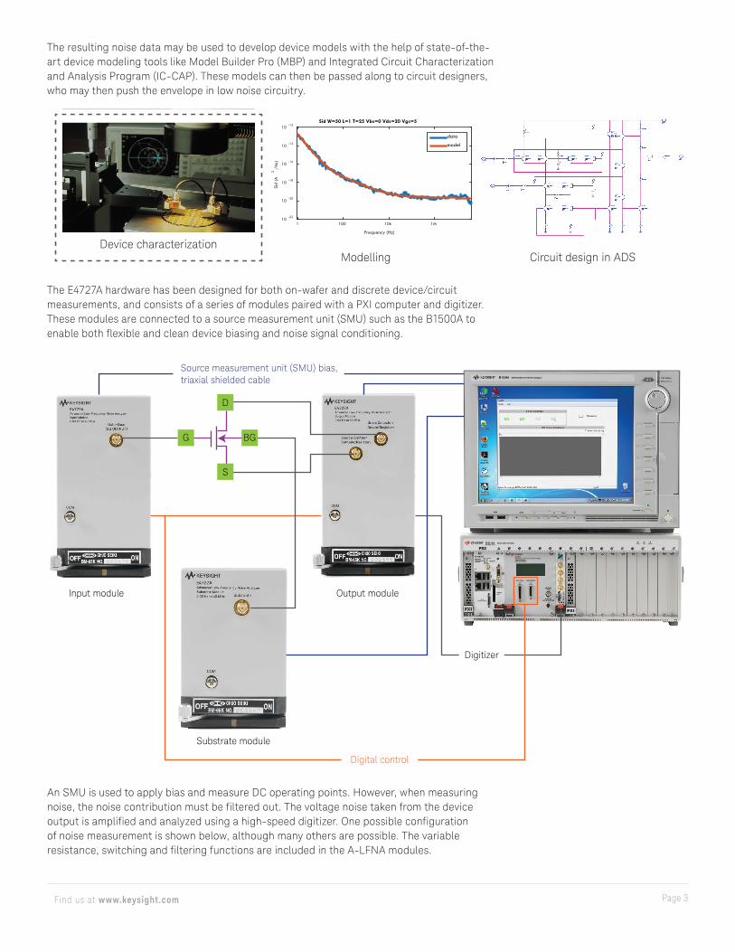
The E4727A hardware has been designed for both on-wafer and discrete device/circuit measurements, and consists of a series of modules paired with a PXI computer and digitizer. These modules are connected to a source measurement unit (SMU) such as the B1500A to enable both flexible and clean device biasing and noise signal conditioning.
An SMU is used to apply bias and measure DC operating points. However, when measuring noise, the noise contribution must be filtered out. The voltage noise taken from the device output is amplified and analyzed using a high-speed digitizer. One possible configuration of noise measurement is shown below, although many others are possible. The variable resistance, switching and filtering functions are included in the A-LFNA modules.
The resulting noise data may be used to develop device models with the help of state-of-the-art device modeling tools like Model Builder Pro (MBP) and Integrated Circuit Characterization and Analysis Program (IC-CAP). These models can then be passed along to circuit designers, who may then push the envelope in low noise circuitry.
Frequency (Hz)
1 100 10k 1M
Sid
(A2
/Hz)
10 -22
10 -20
10 -18
10 -16
10 -14
10 -12Sid W=50 L=1 T=25 Vbs=0 Vds=20 Vgs=5
data
model
Device characterizationModelling Circuit design in ADS
Source measurement unit (SMU) bias, triaxial shielded cable
D
Input module Output module
Substrate module
S
Digital control
Digitizer
G BG

Page 4Find us at www.keysight.com
Different device types require different source and load impedance terminations. The E4727A is the only analyzer in the industry to offer 25 impedance values ranging from 0 ohms to 100 MΩ. The A-LFNA software is able to judiciously select RSource and RLoad based on device type (FET, diode, BJT, etc.) and measured DC characteristics.
The PXI chassis system controller comes equipped with the A-LFNA software integrated with WaferPro express, enabling fast and flexible instrument and prober control. Thus, the engineer may now automate multi-bias, multi-device DC and noise measurements. Measurement speed and accuracy may be adjusted by setting the degree of hardware averaging. The factory provided measurement routines offer a rich set of biasing schemes that can be copied and modified to suit specific needs.
Page 5Find us at www.keysight.com
Measurement Capabilities
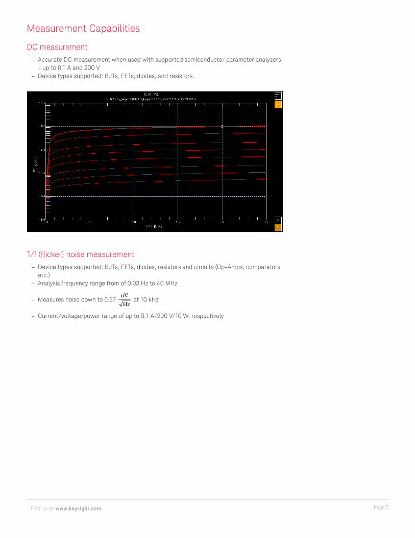
DC measurement – Accurate DC measurement when used with supported semiconductor parameter analyzers
- up to 0.1 A and 200 V – Device types supported: BJTs, FETs, diodes, and resistors.
1/f (flicker) noise measurement – Device types supported: BJTs, FETs, diodes, resistors and circuits (Op-Amps, comparators,
etc.) – Analysis frequency range from of 0.03 Hz to 40 MHz
– Measures noise down to 0.67 nVHz
at 10 kHz
– Current/voltage/power range of up to 0.1 A/200 V/10 W, respectively
Page 6Find us at www.keysight.com
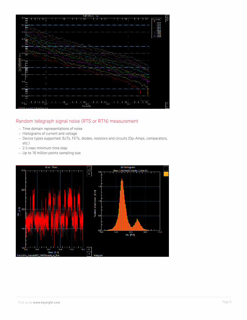
Random telegraph signal noise (RTS or RTN) measurement – Time domain representations of noise – Histograms of current and voltage – Device types supported: BJTs, FETs, diodes, resistors and circuits (Op-Amps, comparators,
etc.) – 2.5 nsec minimum time step – Up to 16 million points sampling size

Page 7Find us at www.keysight.com
E4727A Specifications
Main modulesThe E4727A adopts an innovative modular architecture to minimize system noise.
Module name Key featuresM9018A PXIe mainframe 18-slot chassis, providing central control of E4727A
M9036A embedded PC Windows 7 64-bit (in English)E4727A(K01) interface module LCD display
Digital control of input and output modulesDigitizer A/D converter (digitizer)
E4727A(K02) input module Connects to DUT input portE4727A(K03) output module Connects to DUT output portE4727A(K04) substrate module Connects to DUT substrate/backgateE4727A(K05) test fixture module Fixture for through-hole packaged devicesModule enclosure Grounding enclosure for input, output and substrate modules
E4727A(K01) interface module specificationsResiding in the PXI chassis, the interface module controls the E4727A (K02) input module for gate or base bias and the E4727A (K03) output module for drain or collector bias.
Input module (K02) controlConnector type 36-pin miniature delta ribbon (f)Output module (K03) controlConnector type 26-pin miniature delta ribbon (f)Interlock connectionsInterlock for 4142B BNC(f)Interlock for 4155/4156/B1500/E5260/E5270 16493J

Page 8Find us at www.keysight.com
E4727A(K02) input module specificationsThe input module accepts a voltage or current input from the SMU generates an input bias output signal that is suitable for noise measurements. 3 output configurations are possible:
– Straight pass-through of the SMU input signal for DC characterization – Low pass filtering of the SMU signal followed by a controlled input impedance for noise
measurement – With a 0.01 Hz to 40 MHz signal generator output for device or circuit gain
characterization
LPFNumber of LPFs 2
LPF1 LPF2Cut-off frequency 0.03 Hz 0.53 HzSeries resistance (Rlpf_input) 5 kΩ 300 ΩMaximum voltage ± 50 VDC ± 50 VDCMaximum current ± 0.1 A ± 0.1 AInput resistancesResistor values 0 to 100 MΩ (25 selections)Accuracy ± 0.5%Signal generator circuitOutput signal Sine waveFrequency range 0.01 Hz to 40 MHzFrequency resolution 233 μHz (fout ≤ 30 Hz); 29.1 mHz (fout > 30 Hz)Output amplitude –50 dBm, –60 dBm, or –70 dBm, all ± 5 dB
typicalOutput impedance 50 ΩConnector typesDC Source Measure Unit (SMU) inputs Tri-axial(f) Force and Tri-axial(f) SenseInterface module digital control input 36-pin miniature delta ribbon (f)Gate/Base (SG output) port SMA(f)
Page 9Find us at www.keysight.com
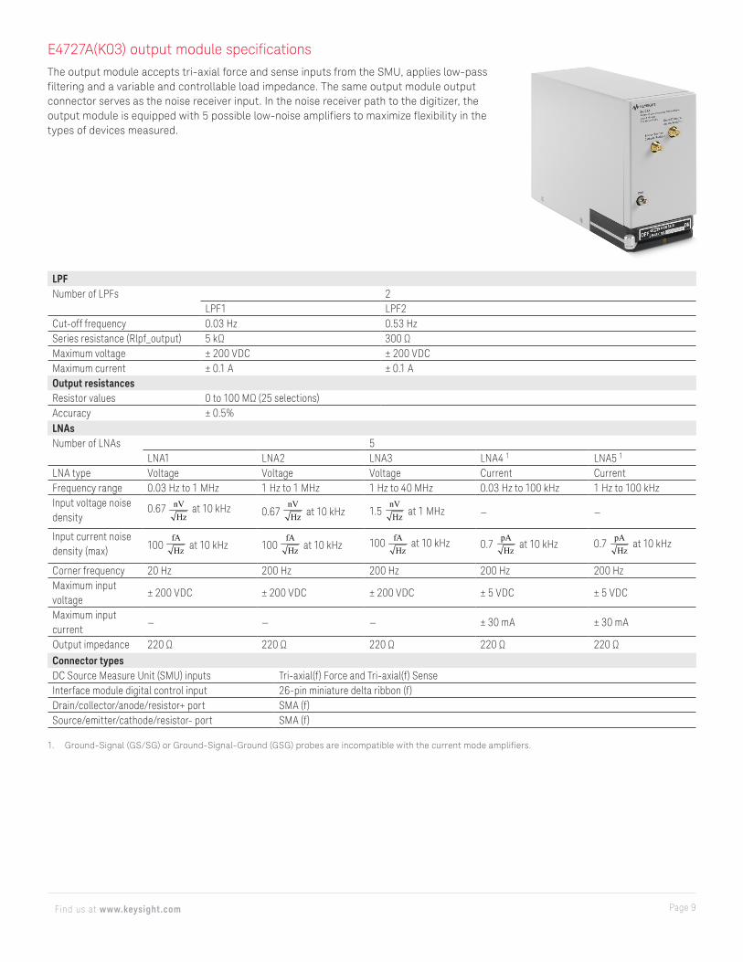
E4727A(K03) output module specificationsThe output module accepts tri-axial force and sense inputs from the SMU, applies low-pass filtering and a variable and controllable load impedance. The same output module output connector serves as the noise receiver input. In the noise receiver path to the digitizer, the output module is equipped with 5 possible low-noise amplifiers to maximize flexibility in the types of devices measured.
LPFNumber of LPFs 2
LPF1 LPF2Cut-off frequency 0.03 Hz 0.53 HzSeries resistance (Rlpf_output) 5 kΩ 300 ΩMaximum voltage ± 200 VDC ± 200 VDCMaximum current ± 0.1 A ± 0.1 AOutput resistancesResistor values 0 to 100 MΩ (25 selections)Accuracy ± 0.5%LNAsNumber of LNAs 5
LNA1 LNA2 LNA3 LNA4 1 LNA5 1
LNA type Voltage Voltage Voltage Current CurrentFrequency range 0.03 Hz to 1 MHz 1 Hz to 1 MHz 1 Hz to 40 MHz 0.03 Hz to 100 kHz 1 Hz to 100 kHzInput voltage noise density
0.67 nVHz
at 10 kHz 0.67 nVHz at 10 kHz 1.5
nVHz at 1 MHz — —
Input current noise density (max) 100
fAHz at 10 kHz 100
fAHz at 10 kHz 100 fA
Hz at 10 kHz 0.7
pAHz at 10 kHz 0.7
pAHz
at 10 kHz
Corner frequency 20 Hz 200 Hz 200 Hz 200 Hz 200 HzMaximum input voltage
± 200 VDC ± 200 VDC ± 200 VDC ± 5 VDC ± 5 VDC
Maximum input current
— — — ± 30 mA ± 30 mA
Output impedance 220 Ω 220 Ω 220 Ω 220 Ω 220 ΩConnector typesDC Source Measure Unit (SMU) inputs Tri-axial(f) Force and Tri-axial(f) SenseInterface module digital control input 26-pin miniature delta ribbon (f)Drain/collector/anode/resistor+ port SMA (f)Source/emitter/cathode/resistor- port SMA (f)
1. Ground-Signal (GS/SG) or Ground-Signal-Ground (GSG) probes are incompatible with the current mode amplifiers.

Page 10Find us at www.keysight.com
Actual Measured Data for Sid=2E-27A2/Hz
Actual Measured Data for Ids=70pA

Page 11Find us at www.keysight.com
LPFNumber of LPFs 1Cut-off frequency 0.08 HzSeries resistance (Rlpf_substrate) 2 kΩMaximum voltage ± 50 VDCMaximum current ± 0.1 AConnectorDC Source Measure Unit (SMU) inputs Tri-axial(f) Force and Tri-axial(f) SenseSubstrate terminal SMA(f)
IC socketType DIP (300 mil and 600 mil)Lead pitch 2.54 mm (100 mil)Maximum number of leads 28ConnectorDrain/collector/ anode/resistor+ SMA(f)Source/emitter/cathode/resistor- SMA(f)Gate/base terminal SMA(f)Substrate terminal SMA(f)
E4727A(K04) substrate module specificationsThe substrate module is a passive device used to pass along a filtered version of the DC bias to a substrate or back-gate node of a device.
E4727A(K05) test fixture module specificationsThe test fixture module is used to facilitate testing of packaged through-hole devices.

Page 12Find us at www.keysight.com
E4727A Software
The A-LFNA software and user interface is built on top of the WaferPro Express measurement platform. Engineers may now manage and automate the full wafer level characterization in a measurement system that is both flexible and expandable. Just as before, those using WaferPro Express can program and sequence high-speed DC, capacitance and RF as parameter measurements, all the while automating wafer prober control. Now with the noise measurement module, they can add noise measurements and analysis to the test suite.
The A-LFNA’s built-in measurement routines make DC and noise measurements turnkey. For example, to measure noise on an N-Type MOSFET, the system automatically chooses the source and load impedances that will best expose the intrinsic device noise. The engineer can accept these recommended settings or make changes, and a noise measurement is initiated. The A-LFNA then measures noise power spectral density (1/f noise) and noise in the time domain (RTN). Resulting data is plotted using a “multiplot” data display window. Various windows tabs help facilitate common tasks such as evaluating device DC operating point and measuring the slope of the power spectral density curve.
Key features – Seamless integration with WaferPro Express measurement platform – Advanced data display and analysis, enabling noise data comparisons and modeling with
respect to bias current – Convenient connectivity to instruments via GPIB and prober systems via LAN IP address – Automated control of all major wafer probing systems, thanks to Keysight’s close
collaboration with Cascade Microtech (auto-align, wafer map, die indexing, etc.) – A-LFNA module features DC measurements, 1/f noise, random telegraph noise and data
analysis – Flexible hardware averaging for throughput-accuracy tradeoffs – Multiple built-in biasing schemes for flicker noise characterization – Measured data compatible with Keysight device modeling software – Guided system calibration procedure – PEL and Python measurement routine language support

Page 13Find us at www.keysight.com
Device type Biasing scheme DescriptionFET SetVg Defines Vgs, Vds, and Vbs as bias conditions
SetId Defines Ids, Vds, and Vbs is as bias conditions. Vgs is determined automatically to achieve target Ids
SetOD Defines threshold voltage (Vth) based on constant-current or gm_max and an offset voltage. Vgs will be automatically set offset from Vth.
BJT SetVb Defines Vbe ,Vce and Vse as bias conditionsSetIb Defines Ib and Vc and Vse as bias conditions. Vbe is determined
automatically to achieve target Ib.SetIc Defines Ic, Vc and Vse as bias conditions. Vbe is determined
automatically to achieve target Ic.Diode SetVa Defines Vac and Vsub as bias conditions
SetIa Defines Iac (diode current) and Vsub as bias conditions. Vac is determined automatically to achieve target Iac.
Resistor SetVr Defines Vr and Vsub as bias conditionsSetIr Defines Ir and Vsub as bias conditions. Vr is set automatically.
Measurement Functions
Built-in biasing schemes

Page 14Find us at www.keysight.com
External instrument control
Supported parameter analyzers – Keysight 4142B (41420A HPSMU, 41421B MPSMU) – Keysight 4155B/C (MPSMU) – Keysight 4156B/C (HRSMU) – Keysight B1500A (B1510A HPSMU, B1511A/B MPSMU, B1517A HRSMU) – Keysight E5260A (E5290A HPSMU, E5291A MPSMU) – Keysight E5270B (E5280B HPSMU, E5281B MPSMU, E5287A HRSMU)
Supported semi-automated probe stationsThe choice of which prober to work with the A-LFNA is an important decision. Conducted noise from the probe station, either from thermal Chuck or servo motors controlling the microscope or positioners may introduce noise in the A-LFNA measurement. Thanks to a close collaboration between Keysight and Cascade Microtech, we are pleased to present semi automatic control of the following probe stations.
– Cascade Summit 12000, lowest noise – Cascade S300 – Cascade Elite300, lowest noise – Cascade PA300 – Cascade CM300, etc.
Note that any probe station not listed above (manual or otherwise) is perfectly acceptable for A-LFNA measurements. The only consideration is that the prober will not be controlled by the A-LFNA software.
Interfaces
Interface DescriptionLAN 2 LAN connectors for connection with embedded PCUSB 4 USB ports at front of PXIe chassis for connection with embedded PCGPIB GPIB interface built into M9036A embedded PCVGA video output External display connector to embedded PCInterlock High-voltage safety mechanism for Keysight 4142B, 4155B/C, 4156B/C, E5260A,
E5270B, B1500A and test fixture module (K05)
System Specifications
Number of DUT terminals 4 for FET and BJT (expandable to 5 or 6 by Opt.022 or Opt. 023)3 for diode and resistor1 for circuit
Maximum bias applied to DUT
Voltage AMP Current AMPGate/Base 50 V – (Rlpf_input+RSource)*IPORT1
Drain/Collector/Diode
200 V – (Rlpf_output+RLoad)*IPORT2 ± 5 V
Substrate 50 V – 2 KΩ *IsubstrateResistor 200 V – (Rlpf_output+RLoad+Rdut)*IPORT2
Maximum RDUT = 10 MΩ N/AMinimum noise floor 2E-27 A2/HzMinimum bias current 70 pA (typ)1/f noise measurement accuracy ± 1.5 dB1/f noise measurement repeatability
± 2.0 dB
Page 15Find us at www.keysight.com
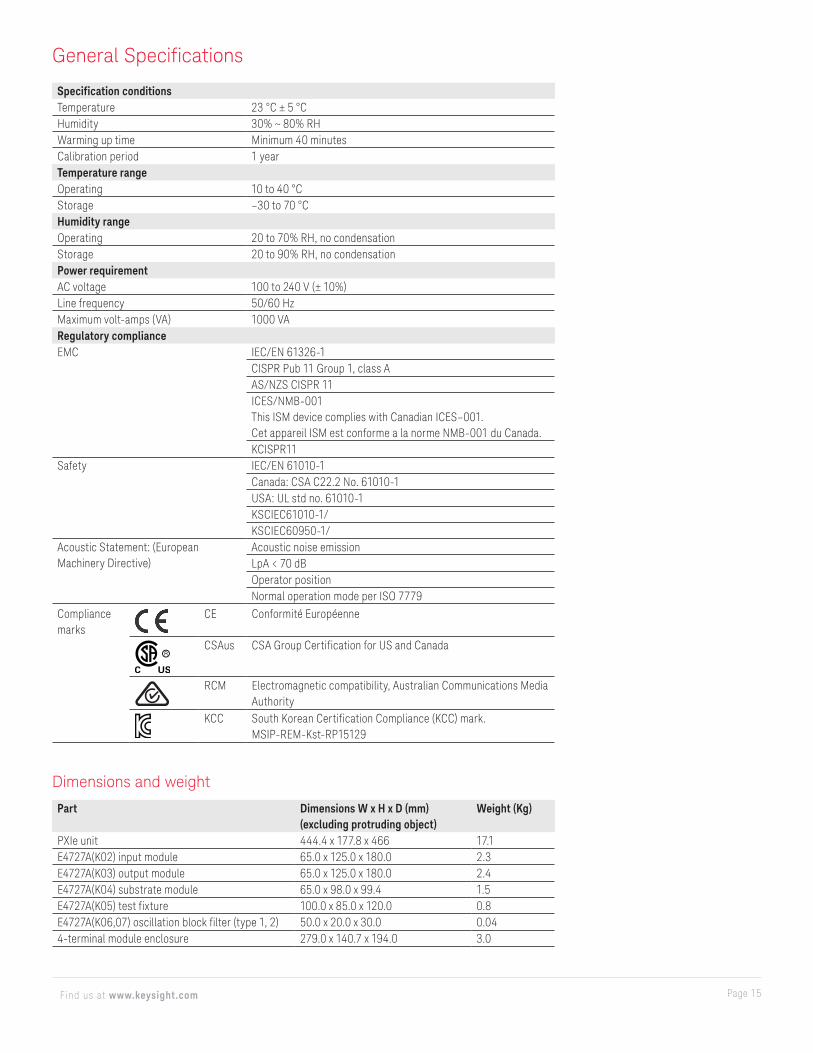
General Specifications
Dimensions and weight
Part Dimensions W x H x D (mm) (excluding protruding object)
Weight (Kg)
PXIe unit 444.4 x 177.8 x 466 17.1E4727A(K02) input module 65.0 x 125.0 x 180.0 2.3E4727A(K03) output module 65.0 x 125.0 x 180.0 2.4E4727A(K04) substrate module 65.0 x 98.0 x 99.4 1.5E4727A(K05) test fixture 100.0 x 85.0 x 120.0 0.8E4727A(K06,07) oscillation block filter (type 1, 2) 50.0 x 20.0 x 30.0 0.044-terminal module enclosure 279.0 x 140.7 x 194.0 3.0
Specification conditionsTemperature 23 °C ± 5 °CHumidity 30% ~ 80% RHWarming up time Minimum 40 minutesCalibration period 1 yearTemperature rangeOperating 10 to 40 °CStorage –30 to 70 °CHumidity rangeOperating 20 to 70% RH, no condensationStorage 20 to 90% RH, no condensationPower requirementAC voltage 100 to 240 V (± 10%)Line frequency 50/60 HzMaximum volt-amps (VA) 1000 VARegulatory complianceEMC IEC/EN 61326-1
CISPR Pub 11 Group 1, class AAS/NZS CISPR 11ICES/NMB-001This ISM device complies with Canadian ICES–001.Cet appareil ISM est conforme a la norme NMB-001 du Canada.KCISPR11
Safety IEC/EN 61010-1Canada: CSA C22.2 No. 61010-1USA: UL std no. 61010-1KSCIEC61010-1/KSCIEC60950-1/
Acoustic Statement: (European Machinery Directive)
Acoustic noise emissionLpA < 70 dBOperator positionNormal operation mode per ISO 7779
Compliance marks
CE Conformité Européenne
CSAus CSA Group Certification for US and Canada
RCM Electromagnetic compatibility, Australian Communications Media Authority
KCC South Korean Certification Compliance (KCC) mark. MSIP-REM-Kst-RP15129

Page 16Find us at www.keysight.com
RTN and 1/f noise measurement system comparison
E4727AAdvanced Low-Frequency Analyzer
E4727E3Automated RTN software for
B1500AMeasurement software E4727P3
A-LFNA measurement and programming bundle softwareE4727E3
WGFMU measurement bundle software
License type Floating Node-lockedSupported instrument E4727A A-LFNA B1500A with B1530A
WGFMU (Optional)B1500A with B1530A WGFMU
Target device FET, BJT, Diode, Resistor, Circuit FETDevice terminal number 3, 4, 5, 6 3Maximum bias voltage ± 200 V ± 10 VMaximum bias current ± 100 mA ± 10 mABias Mode for FET SetVg, SetId, SetOD, SetODvdlinNoise floor 2E-27 A2/Hz 1E-25 A2/HzAnalog frequency bandwidth
30 m to 40 MHz 1 m to 16 MHz
Frequency domain measurement
Minimum frequency 30 mHz 1 mHzMaximum frequency 40 MHz 16 MHz
Time domain measurement
Maximum sampling frequency
400 MHz 200 MHz
Minimum sampling interval
2.5 nsec 5 nsec
Maximum sampling number
224=16,777,216 221=2,097,152
Controller PC M9036A PXIe embedded controller Windows PCGPIB interface M9036A built-in GPIB interface (Micro-D 25 pin) USB GPIB interface (Keysight
82357B, NI GPIB-USB-HS)
Automated RTN Solution Using E4727E3 and B1500A
E4727E3 efficiently performs at a low cost an automated RTN measurement on the wafer using the B1500A Semiconductor Device Analyzer with the B1530A Waveform Generator/Fast Measurement Unit (WGFMU). It can improve the efficiency of RTN measurement and data analysis including wafer prober control.
Key features – Automated measurement without programing – Auto prober control – Wafer mapping – Single data display for multi decade in frequency domain – Upgradeable from your existing B1500A
Page 17Find us at www.keysight.com
Ordering Information
Automated noise measurement with A-LFNAE4727A Advanced low-frequency noise analyzerE4727A-022 Add one extra substrate module for 5-terminal device characterizationE4727A-023 Add two extra substrate modules for 6-terminal device characterizationE4727A-031 Connection plate for PA300E9000S 12 month hardware warrantyE4727P3 WaferPro Express A-LFNA and WGFMU measurement and programming bundle
software licenseR-35E-001-B Floating single site licenseR-36E-002-L 12M upgrades and support contract - Floating single siteR-36E-002-X 24M upgrades and support contract - Floating single siteR-36E-002-Y 36M upgrades and support contract - Floating single siteAutomated noise measurement with WGFMU (Typical configuration example)B1500A Semiconductor device analyzer mainframeB1500A-A00 Empty package for custom solutionB1500A-A30/A31 WGFMU add-on package or WGFMU add-on package with connector adaptersB1500A-A3P WGFMU probe cable kitE4727E3 WaferPro Express WGFMU measurement bundle software licenseR-35E-001-A Node-locked LicenseR-36E-001-L 12M upgrades and support contract - Node-lockR-36E-001-X 24M upgrades and support contract - Node-lockR-36E-001-Y 36M upgrades and support contract - Node-lock
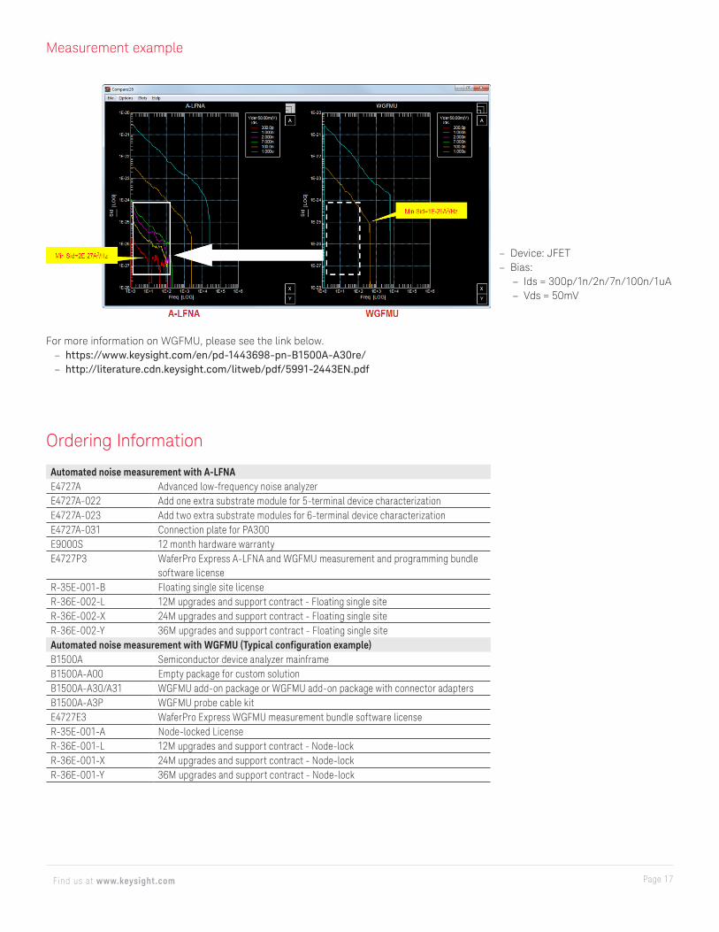
Measurement example
For more information on WGFMU, please see the link below. – https://www.keysight.com/en/pd-1443698-pn-B1500A-A30re/ – http://literature.cdn.keysight.com/litweb/pdf/5991-2443EN.pdf
– Device: JFET – Bias:
– Ids = 300p/1n/2n/7n/100n/1uA – Vds = 50mV

This information is subject to change without notice. © Keysight Technologies, 2015 - 2018, Published in USA, September 28, 2018, 5991-4280EN
Page 18Find us at www.keysight.com
Learn more at: www.keysight.comFor more information on Keysight Technologies’ products, applications or services,
please contact your local Keysight office. The complete list is available at:
www.keysight.com/find/contactus
Keysight IC-CAP
– Device Modeling Software – www.keysight.com/find/eesof-iccap
Keysight MBP
– Turn-key Device Model Extraction Solutions – www.keysight.com/find/eesof-mbp
Keysight MQA
– Device Model Validation Software – www.keysight.com/find/eesof-mqa
Keysight WaferPro Express
– On-wafer Measurement Program – www.keysight.com/find/eesof-waferpro-express