data sheet sky65135: wlan power amplifier
TRANSCRIPT

Skyworks Solutions, Inc. • Phone [781] 376-3000 • Fax [781] 376-3100 • [email protected] • www.skyworksinc.com 200436D • Skyworks Proprietary and Confidential information • Products and Product Information are Subject to Change Without Notice • March 28, 2007 1
DATA SHEET
SKY65135: WLAN Power Amplifier Applications
• IEEE802.11 b/g WLAN
• ISM band
• WCS fixed wireless
• Wireless access nodes
Features
• Linear output power of +31 dBm for IEEE802.11b mask
• Linear output power of +30 dBm for IEEE802.11g mask
• Three percent EVM at POUT >+27 dBm
• High gain of 33 dB
• Output power detector: 20 dB dynamic range
• Superior gain flatness
• Internal RF match and bias circuits
• Small footprint, MCM (20-pin, 6 x 6 mm) Pb-free (MSL3, 250 °C per JEDEC J-STD-020) SMT package
Skyworks offers lead (Pb)-free RoHS (Restriction of Hazardous Substances) compliant packaging.
Description Skyworks SKY65135 is a Microwave Monolithic Integrated Circuit (MMIC) Power Amplifier (PA) with superior output power, linearity, and efficiency. These features make the SKY65135 ideal for Wireless Local Area Network (WLAN) applications.
The device is fabricated using Skyworks high reliability Indium Gallium Phosphide (InGaP) Heterojunction Bipolar Transistor (HBT) technology. The device is internally matched and mounted in a 20-pin, 6 x 6 mm Multi-Chip Module (MCM) Surface-Mounted Technology (SMT) package, which allows for a highly manufacturable low cost solution.
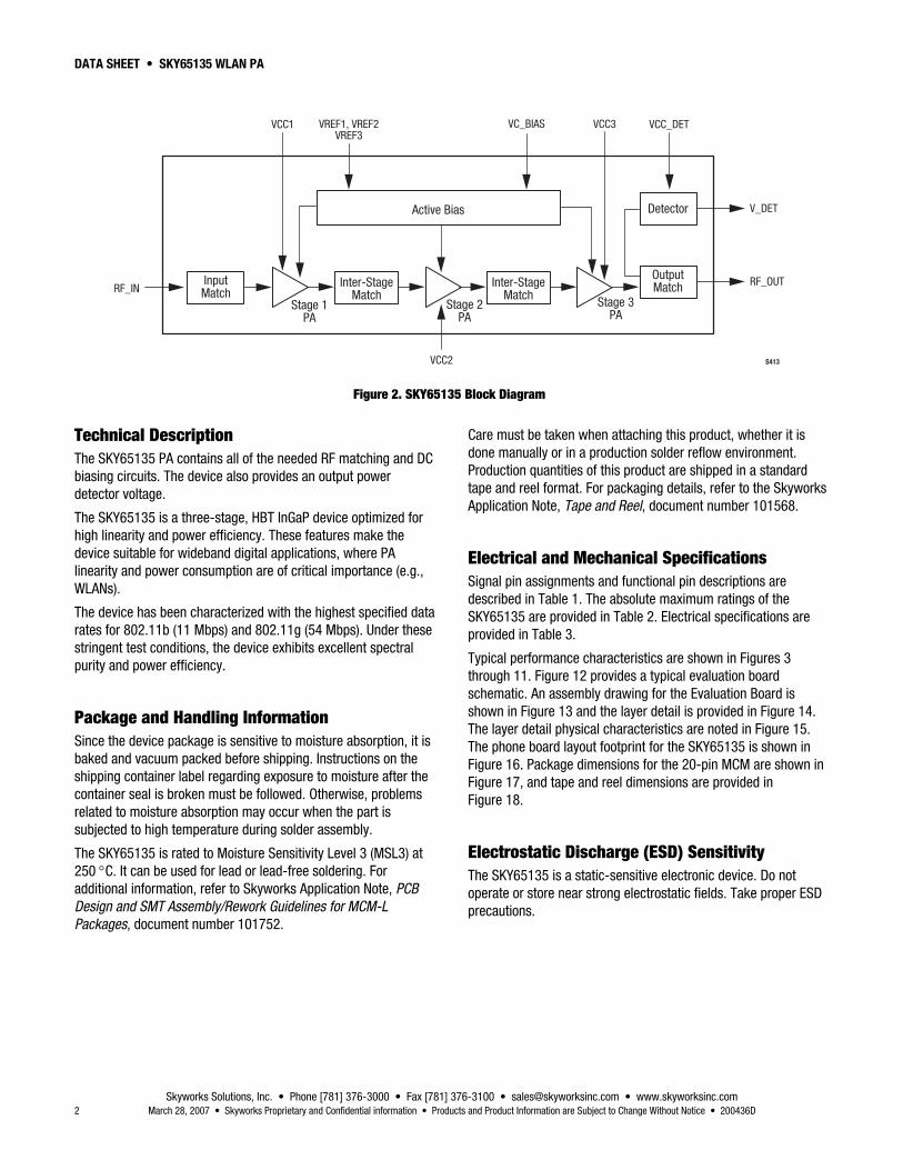
The device package and pinout for the 20-pin MCM are shown in Figure 1. A block diagram of the SKY65135 is shown in Figure 2.
GND 1
2
3
4
5
6
16
15
14
13
12
117 8 9 10
20 19 18 17
VREF
3
GND
RF_O
UT
GND
GND
GND
RF_I
N
GND
GND
GND
VC_BIAS
VREF1
VREF2
VCC1
VCC_DET
V_DET
VCC2
VDET_CNTL
VCC3
S414
Figure 1. SKY65135 Pinout – 20-Pin MCM (Top View)
DATA SHEET • SKY65135 WLAN PA
Skyworks Solutions, Inc. • Phone [781] 376-3000 • Fax [781] 376-3100 • [email protected] • www.skyworksinc.com 2 March 28, 2007 • Skyworks Proprietary and Confidential information • Products and Product Information are Subject to Change Without Notice • 200436D
RF_IN
VCC1 VREF1, VREF2VREF3
VC_BIAS VCC_DET
VCC2
VCC3
RF_OUTInputMatch
OutputMatch
Stage 1 PA
Stage 2PA
Stage 3PA
Active Bias
Inter-StageMatch
S413
Inter-StageMatch
V_DETDetector
Figure 2. SKY65135 Block Diagram
Technical Description The SKY65135 PA contains all of the needed RF matching and DC biasing circuits. The device also provides an output power detector voltage.
The SKY65135 is a three-stage, HBT InGaP device optimized for high linearity and power efficiency. These features make the device suitable for wideband digital applications, where PA linearity and power consumption are of critical importance (e.g., WLANs).
The device has been characterized with the highest specified data rates for 802.11b (11 Mbps) and 802.11g (54 Mbps). Under these stringent test conditions, the device exhibits excellent spectral purity and power efficiency.
Package and Handling Information Since the device package is sensitive to moisture absorption, it is baked and vacuum packed before shipping. Instructions on the shipping container label regarding exposure to moisture after the container seal is broken must be followed. Otherwise, problems related to moisture absorption may occur when the part is subjected to high temperature during solder assembly.
The SKY65135 is rated to Moisture Sensitivity Level 3 (MSL3) at 250 °C. It can be used for lead or lead-free soldering. For additional information, refer to Skyworks Application Note, PCB Design and SMT Assembly/Rework Guidelines for MCM-L Packages, document number 101752.
Care must be taken when attaching this product, whether it is done manually or in a production solder reflow environment. Production quantities of this product are shipped in a standard tape and reel format. For packaging details, refer to the Skyworks Application Note, Tape and Reel, document number 101568.
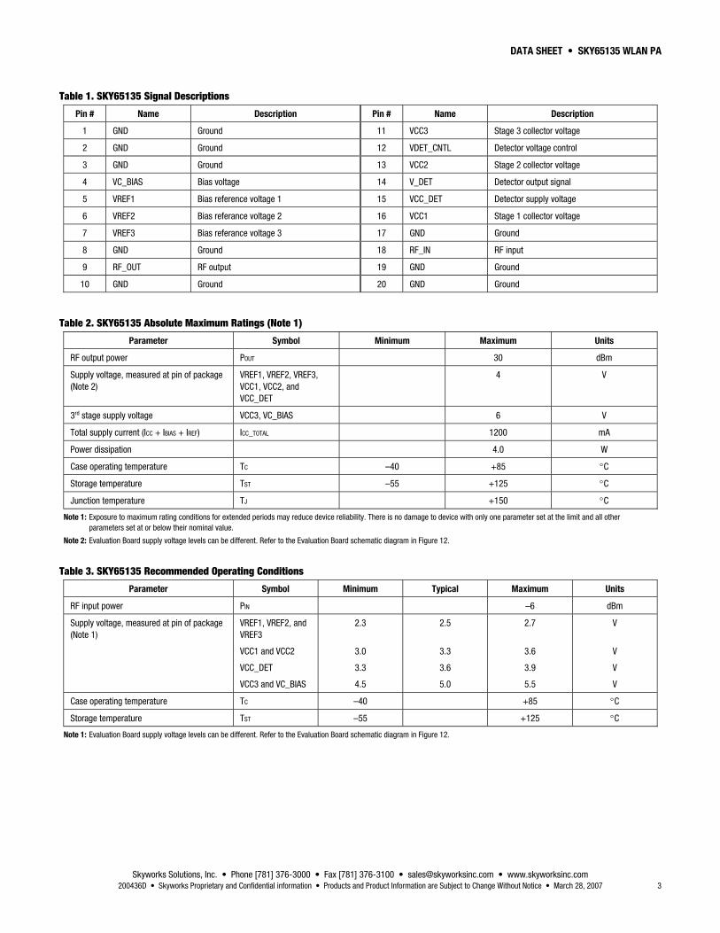
Electrical and Mechanical Specifications Signal pin assignments and functional pin descriptions are described in Table 1. The absolute maximum ratings of the SKY65135 are provided in Table 2. Electrical specifications are provided in Table 3.
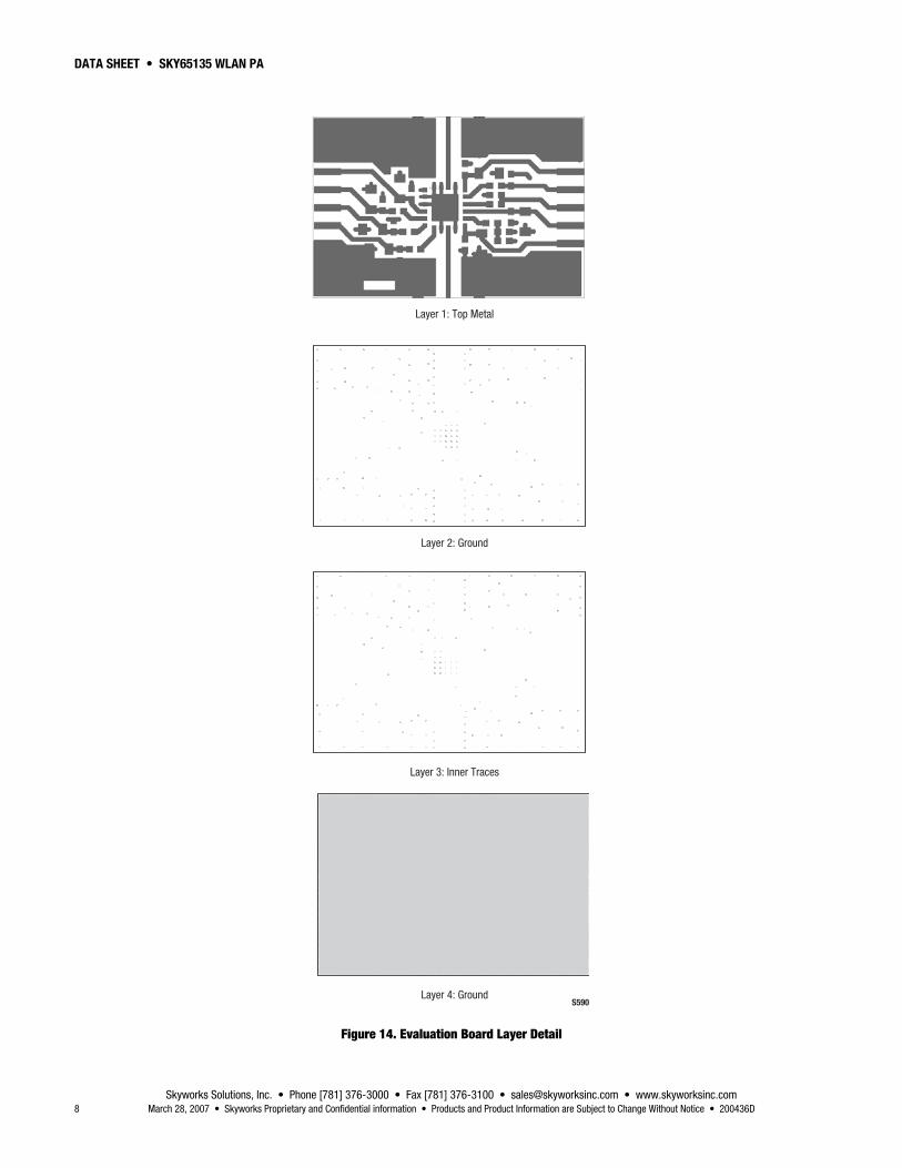
Typical performance characteristics are shown in Figures 3 through 11. Figure 12 provides a typical evaluation board schematic. An assembly drawing for the Evaluation Board is shown in Figure 13 and the layer detail is provided in Figure 14. The layer detail physical characteristics are noted in Figure 15. The phone board layout footprint for the SKY65135 is shown in Figure 16. Package dimensions for the 20-pin MCM are shown in Figure 17, and tape and reel dimensions are provided in Figure 18.
Electrostatic Discharge (ESD) Sensitivity The SKY65135 is a static-sensitive electronic device. Do not operate or store near strong electrostatic fields. Take proper ESD precautions.
DATA SHEET • SKY65135 WLAN PA
Skyworks Solutions, Inc. • Phone [781] 376-3000 • Fax [781] 376-3100 • [email protected] • www.skyworksinc.com 200436D • Skyworks Proprietary and Confidential information • Products and Product Information are Subject to Change Without Notice • March 28, 2007 3
Table 1. SKY65135 Signal Descriptions
Pin # Name Description Pin # Name Description
1 GND Ground 11 VCC3 Stage 3 collector voltage
2 GND Ground 12 VDET_CNTL Detector voltage control
3 GND Ground 13 VCC2 Stage 2 collector voltage
4 VC_BIAS Bias voltage 14 V_DET Detector output signal
5 VREF1 Bias reference voltage 1 15 VCC_DET Detector supply voltage
6 VREF2 Bias referance voltage 2 16 VCC1 Stage 1 collector voltage
7 VREF3 Bias referance voltage 3 17 GND Ground
8 GND Ground 18 RF_IN RF input
9 RF_OUT RF output 19 GND Ground
10 GND Ground 20 GND Ground
Table 2. SKY65135 Absolute Maximum Ratings (Note 1)
Parameter Symbol Minimum Maximum Units
RF output power POUT 30 dBm
Supply voltage, measured at pin of package (Note 2)
VREF1, VREF2, VREF3, VCC1, VCC2, and VCC_DET
4 V
3rd stage supply voltage VCC3, VC_BIAS 6 V
Total supply current (ICC + IBIAS + IREF) ICC_TOTAL 1200 mA
Power dissipation 4.0 W
Case operating temperature TC –40 +85 °C
Storage temperature TST –55 +125 °C
Junction temperature TJ +150 °C
Note 1: Exposure to maximum rating conditions for extended periods may reduce device reliability. There is no damage to device with only one parameter set at the limit and all other parameters set at or below their nominal value.
Note 2: Evaluation Board supply voltage levels can be different. Refer to the Evaluation Board schematic diagram in Figure 12.
Table 3. SKY65135 Recommended Operating Conditions
Parameter Symbol Minimum Typical Maximum Units
RF input power PIN –6 dBm
Supply voltage, measured at pin of package (Note 1)
VREF1, VREF2, and VREF3
VCC1 and VCC2
VCC_DET
VCC3 and VC_BIAS
2.3
3.0
3.3
4.5
2.5
3.3
3.6
5.0
2.7
3.6
3.9
5.5
V
V
V
V
Case operating temperature TC –40 +85 °C
Storage temperature TST –55 +125 °C
Note 1: Evaluation Board supply voltage levels can be different. Refer to the Evaluation Board schematic diagram in Figure 12.

DATA SHEET • SKY65135 WLAN PA
Skyworks Solutions, Inc. • Phone [781] 376-3000 • Fax [781] 376-3100 • [email protected] • www.skyworksinc.com 4 March 28, 2007 • Skyworks Proprietary and Confidential information • Products and Product Information are Subject to Change Without Notice • 200436D
Table 4. SKY65135 Electrical Specifications (VCC1 = VCC2 = 3.3 V, VCC3 = 5 V, TC = +25 °C, Test Frequency = 2.442 GHz unless otherwise noted)
Parameter Symbol Test Condition Min Typical Max Units
Using IEEE802.11b Complimentary Code Keying Input Signal, Data Rate = 11 Mbps
Total supply current ICC_TOTAL 1150 mA
Output power (Note 1) POUT 31 dBm
Power added efficiency (Note 2) PAE 25 %
Ramp-up/ramp-down (Note 3) TS <0.5 µs
Using IEEE802.11g Orthogonal Frequency Division Multiplexing Input Signal, Data Rate = 54 Mbps
Total supply current ICC_TOTAL 1050 mA
Output power (Note 4) POUT 30 dBm
Output power @ EVM = 3% POUT_EVM 27 dBm
Power added efficiency (Note 2) PAE 22 %
Using Continuous Wave Input Signals
Small signal gain G PIN = –25 dBm 31.5 33 34.5 dB
Gain flatness over band From 2.4 GHz to 2.5 GHz ±0.5 dB
Gain flatness over channel (16.25 MHz) Over any 16.25 MHz within band
±0.1 dB
Output power @ 1 dB compression P1dB PIN = 0 dBm 32 33 dBm
Output IP3 OIP3 PTONE = +27 dBm, Delta_freq = 5 MHz
42 dBm
Quiescent Current IQ No RF input 400 450 mA
Noise Figure NF 5 6 dB
Power added efficiency @ P1dB PAE 25 34 %
Note 1: Defined as the maximum power level for which the IEEE802.11b transmit mask requirements are met.
Note 2: Measured at the specified average output RF power and modulation type.
Note 3: Ramp-up and ramp-down times are defined from the 10% to 90% power points.
Note 4: Defined as the maximum power level for which the IEEE802.11g transmit mask requirements are met.

DATA SHEET • SKY65135 WLAN PA
Skyworks Solutions, Inc. • Phone [781] 376-3000 • Fax [781] 376-3100 • [email protected] • www.skyworksinc.com 200436D • Skyworks Proprietary and Confidential information • Products and Product Information are Subject to Change Without Notice • March 28, 2007 5
3012 14 16 18 2010 24 26 28 30 32 3422
31
32
33
34
35
36
Gain
(dB)
POUT (dBm)
Figure 3. Typical Gain vs POUT @ 2.442 GHz
2.41 2.42 2.43 2.44 2.45 2.46 2.47 2.48 2.49 2.502.40
5.2
5.0
4.8
4.6
4.4
4.2
4.0
5.4
5.6
5.8
6.0
Nois
e Fi
gure
(dB)
Frequency (GHz)
Figure 5. Typical Noise Figure Performance vs Frequency
Frequency (GHz)
Rela
tive
Pow
er (d
B)
–50
–60
–40
–30
–20
–10
+10
0
2.411 2.417 2.423 2.430 2.436 2.442 2.448 2.454 2.461 2.467 2.473
IEEE802.11bSpecification Mask
POUT = +31 dBm
Figure 7. Output Spectrum Response for 802.11b CCK-Coded @ 2.442 GHz and POUT = 31 dBm
2.41 2.42 2.43 2.44 2.45 2.46 2.47 2.48 2.49 2.502.40
32.0
33.0
34.0
35.0
Gain
(dB)
Frequency (GHz)
Figure 4. Typical Gain vs Frequency Response
Frequency (GHz)
Rela
tive
Pow
er (d
B)
–50
–40
–30
–20
–10
0
+10
2.411 2.417 2.423 2.430 2.436 2.442 2.448 2.454 2.461 2.467 2.473
POUT = +30 dBm
IEEE802.11gSpecification Mask
Figure 6. Output Spectrum Response for 802.11g @ 2.442 GHz and POUT = 30 dBm
POUT (dBm)
0.2
0
0.4
0.6
0.8
1.0
1.2
1.4
1.6
1.8
10 12 14 16 18 20 22 24 26 28 30 32 34
Dete
ctor
Vol
tage
(V)
Figure 8. Detector Output Voltage vs RF Output Power @ 2.442 GHz

DATA SHEET • SKY65135 WLAN PA
Skyworks Solutions, Inc. • Phone [781] 376-3000 • Fax [781] 376-3100 • [email protected] • www.skyworksinc.com 6 March 28, 2007 • Skyworks Proprietary and Confidential information • Products and Product Information are Subject to Change Without Notice • 200436D
0.5
2.5
1.5
3.0
2.0
1.0
3.5
4.0
4.5
5.0
5.5
6.0
23 24 25 26 27 28 29
Output Power (dBm)
EVM
(%)
Figure 9. EVM vs POUT for 802.11g
5
10
0
15
20
25
30
35
40
14 16 18 20 22 24 26 28 30 3432
Output Power (dBm)
PAE
(%)
Figure 11. PAE vs Output Power
300
100
400
200
0
500
600
700
800
900
1000
14 16 18 20 22 24 26 28 30
Output Power (dBm)
Curr
ent (
mA)
ICC_TOTAL
ICC1
ICC2
ICC3×
× × × × × × × × × × ××
Figure 10. Individual Stage Currents and Total Current vs RF Output Power

DATA SHEET • SKY65135 WLAN PA
Skyworks Solutions, Inc. • Phone [781] 376-3000 • Fax [781] 376-3100 • [email protected] • www.skyworksinc.com 200436D • Skyworks Proprietary and Confidential information • Products and Product Information are Subject to Change Without Notice • March 28, 2007 7
1
20
SKY65135
GND
2 GND
3
4
GND
VC_BIASBias VoltageC18.2 pF
R2200 Ω
R1750 Ω
C1110 μF
C12DNI
C13DNI
C14DNI
5 VREF1ReferenceVoltage 1
C28.2 pF
6 VREF2 11VCC37
VREF
3GN
D
8GN
DReferenceVoltage 2
C38.2 pF
ReferenceVoltage 3
R3270 Ω
C48.2 pF C10
8.2 pFC1710 μF
C9270 pF
C88.2 pF
C1610 μF
C58.2 pF
C1510 μF
10GN
D
9RF
_OUT
19
GND
18
RF_I
N
17
GND
Collector Voltage(Stage 3)
Collector Voltage(Stage 2)
Collector Voltage(Stage 1)
Detector Output
Detector SupplyVoltage
12
13
VDET_CNTL
VCC2
14VDET
15VCC_DET
R451 Ω
L30 Ω
C63300 pF
L1300 Ω
C78.2 pF
L227 nH
16VCC1
S702
Note: Evaluation Board material: four-layer Rogers 4003-12, εr = 3.38.
Some component labels may be different than the corresponding component symbol shown here. Component values, however, are accurate as of the date of this Data Sheet.
Figure 12. SKY65135 Evaluation Board Schematic
J3
J2
J4
S588
R1
C12 C2
C11 C1
C5
C6
C8
R4
C9C17C10R3
R2
C3
C4C14
C13
C16
L1
C7
L2
L3
C15
Figure 13. Evaluation Board Assembly Drawing
DATA SHEET • SKY65135 WLAN PA
Skyworks Solutions, Inc. • Phone [781] 376-3000 • Fax [781] 376-3100 • [email protected] • www.skyworksinc.com 8 March 28, 2007 • Skyworks Proprietary and Confidential information • Products and Product Information are Subject to Change Without Notice • 200436D
Layer 1: Top Metal
Layer 3: Inner Traces
Layer 4: Ground
Layer 2: Ground
S590
Figure 14. Evaluation Board Layer Detail

DATA SHEET • SKY65135 WLAN PA
Skyworks Solutions, Inc. • Phone [781] 376-3000 • Fax [781] 376-3100 • [email protected] • www.skyworksinc.com 200436D • Skyworks Proprietary and Confidential information • Products and Product Information are Subject to Change Without Notice • March 28, 2007 9
S573
Name Thickness (mils) Material εr
L1 1.4 Cu, 1 oz. –
Lam1 12 Rogers 4003-12 3.38
L2_GND 1.4 Cu, 1 oz –
Lam2 4 FR4-4 4.35
L3_GND 1.4 Cu, 1 oz. –
Lam3 12 FR4-12 4.35
L4 1.4 Cu, 1 oz. –
Cross Section
Figure 15. Layer Detail Physical Characteristics

DATA SHEET • SKY65135 WLAN PA
Skyworks Solutions, Inc. • Phone [781] 376-3000 • Fax [781] 376-3100 • [email protected] • www.skyworksinc.com 10 March 28, 2007 • Skyworks Proprietary and Confidential information • Products and Product Information are Subject to Change Without Notice • 200436D
S965
Stencil ApertureTop View
MetallizationTop View
Solder Mask OpeningTop View
6.3
2X 1.7
6.3
1.0 Typical
6.4
6.4
Stencil aperture size for centerground pads should be 80% to100% (by area) of the soldermask opening.
Component outline
Pin 1
Component outline
All measurements are in millimeters
20X 0.85
20X 0.6
Thermal Via Array ∅0.3 mmon 0.6 mm pitch.
Additional vias will improvethermal performance.
Note: Thermal vias should be tented and filled with solder mask: 30 to 35 µm Cu plating recommended.
6.3
1.0 Typical
1.0 Typical
2X 1.7
2X 1.7
6.3
0.6 Typical
Component outline
2X 1.7
20X 0.5
20X 0.75
20X 0.5
20X 0.750.25 Typical
0.6 Typical
Pin 20
Pin 1
Pin 20
Pin 1
Pin 20
Figure 16. SKY65135 Phone Board Layout Footprint

DATA SHEET • SKY65135 WLAN PA
Skyworks Solutions, Inc. • Phone [781] 376-3000 • Fax [781] 376-3100 • [email protected] • www.skyworksinc.com 200436D • Skyworks Proprietary and Confidential information • Products and Product Information are Subject to Change Without Notice • March 28, 2007 11
Pin 1
Top View Side View Bottom View
Detail A
A
Metal PadEdge
1.45 ± 0.1
0.5 ± 0.10.1
0.5 ± 0.05
All dimensions are in millimetersDimensioning and tolerancing accordingto ASME Y14.5M-1994 S416
B6
A
6
C
0.10.15 A B C
4X 2.5
4X 1.5
(2.75)
(2.0
75)
4X 0.5
2X 1.9
8X 2.9
4X R0.2
12X
2.9
4X 1
.5
4X 0
.5
2X 1
.9
Solder Mask Opening
20X SMT Pad
Pin 1
Pin 20
0.2 A B C
A B C0.15
(∅0.3) Solder Mask Opening
∅0.15 Metal PadPin 1 Indicator
Figure 17. SKY65135 20-Pin MCM Package Dimensions

DATA SHEET • SKY65135 WLAN PA
Skyworks Solutions, Inc. • Phone [781] 376-3000 • Fax [781] 376-3100 • [email protected] • www.skyworksinc.com 12 March 28, 2007 • Skyworks Proprietary and Confidential information • Products and Product Information are Subject to Change Without Notice • 200436D
C1222
Notes:1. Carrier tape: black conductive polystyrene2. Cover tape material: transparent conductive PSA3. Cover tape size: 9.3 mm width4. All dimensions are in millimeters A
B
2.00 ± 0.05
∅1.55 ± 0.050.30 ± 0.05
5o Max.
5o Max.
6.30
1.75 ± 0.10
∅1.50 Min.
5.50
± 0
.05
8.00 4.00
A
B
B
A
1.70
12.0
0 ±
0.3
0
6.30
Pin #1Indicator
Figure 18. SKY65135 20-Pin MCM Tape and Reel Dimensions
DATA SHEET • SKY65135 WLAN PA
Skyworks Solutions, Inc. • Phone [781] 376-3000 • Fax [781] 376-3100 • [email protected] • www.skyworksinc.com 200436D • Skyworks Proprietary and Confidential information • Products and Product Information are Subject to Change Without Notice • March 28, 2007 13
Ordering Information Model Name Manufacturing Part Number Evaluation Kit Part Number
SKY65135 WLAN Power Amplifier SKY65135-21 (Pb-free package) TW13-D122
Copyright © 2005, 2006, 2007 Skyworks Solutions, Inc. All Rights Reserved.
Information in this document is provided in connection with Skyworks Solutions, Inc. (“Skyworks”) products or services. These materials, including the information contained herein, are provided by Skyworks as a service to its customers and may be used for informational purposes only by the customer. Skyworks assumes no responsibility for errors or omissions in these materials or the information contained herein. Skyworks may change its documentation, products, services, specifications or product descriptions at any time, without notice. Skyworks makes no commitment to update the materials or information and shall have no responsibility whatsoever for conflicts, incompatibilities, or other difficulties arising from any future changes.
No license, whether express, implied, by estoppel or otherwise, is granted to any intellectual property rights by this document. Skyworks assumes no liability for any materials, products or information provided hereunder, including the sale, distribution, reproduction or use of Skyworks products, information or materials, except as may be provided in Skyworks Terms and Conditions of Sale.
THE MATERIALS, PRODUCTS AND INFORMATION ARE PROVIDED “AS IS” WITHOUT WARRANTY OF ANY KIND, WHETHER EXPRESS, IMPLIED, STATUTORY, OR OTHERWISE, INCLUDING FITNESS FOR A PARTICULAR PURPOSE OR USE, MERCHANTABILITY, PERFORMANCE, QUALITY OR NON-INFRINGEMENT OF ANY INTELLECTUAL PROPERTY RIGHT; ALL SUCH WARRANTIES ARE HEREBY EXPRESSLY DISCLAIMED. SKYWORKS DOES NOT WARRANT THE ACCURACY OR COMPLETENESS OF THE INFORMATION, TEXT, GRAPHICS OR OTHER ITEMS CONTAINED WITHIN THESE MATERIALS. SKYWORKS SHALL NOT BE LIABLE FOR ANY DAMAGES, INCLUDING BUT NOT LIMITED TO ANY SPECIAL, INDIRECT, INCIDENTAL, STATUTORY, OR CONSEQUENTIAL DAMAGES, INCLUDING WITHOUT LIMITATION, LOST REVENUES OR LOST PROFITS THAT MAY RESULT FROM THE USE OF THE MATERIALS OR INFORMATION, WHETHER OR NOT THE RECIPIENT OF MATERIALS HAS BEEN ADVISED OF THE POSSIBILITY OF SUCH DAMAGE.
Skyworks products are not intended for use in medical, lifesaving or life-sustaining applications, or other equipment in which the failure of the Skyworks products could lead to personal injury, death, physical or environmental damage. Skyworks customers using or selling Skyworks products for use in such applications do so at their own risk and agree to fully indemnify Skyworks for any damages resulting from such improper use or sale.
Customers are responsible for their products and applications using Skyworks products, which may deviate from published specifications as a result of design defects, errors, or operation of products outside of published parameters or design specifications. Customers should include design and operating safeguards to minimize these and other risks. Skyworks assumes no liability for applications assistance, customer product design, or damage to any equipment resulting from the use of Skyworks products outside of stated published specifications or parameters.
Skyworks, the Skyworks symbol, and “Breakthrough Simplicity” are trademarks or registered trademarks of Skyworks Solutions, Inc., in the United States and other countries. Third-party brands and names are for identification purposes only, and are the property of their respective owners. Additional information, including relevant terms and conditions, posted at www.skyworksinc.com, are incorporated by reference.