data terminal technical information - · pdf file1.0 introduction the 02620-60088 ... and a...
TRANSCRIPT

HP 1 ~52~~ 0
PROCESSOR MODULE
Manual Part No. 13220-91088
REVISED
AUG-1.4-B1
DATA TERMINAL TECHNICAL INFORMATION
HEWLETT~PACKARD
Printed in U.S.A.

13220 Processor Module
13220-91088/02 REV AUG-14-81
1.0 INTRODUCTION
The 02620-60088 Processor PCA perforMs the terMinal logic functions for the 2623A terMinal. Its operation is based on the Z80A Microprocessor, National SeMiconductor 8367 CRT Controller (eRTC), and a proM based Microsequenced graphics controller.
The control and I/O section of the Processor peA provides control signals, input/output and data processing functions. The MeMory section provides 16K bytes of dynaMic RAM for character display MeMory, scratch pad MeMory, data buffers and space for up to six 4K or 8K byte ROMs of which 40K are used for cOMplete terMinal operation (4K of ROM optional with integral printer). The Graphics MeMory subsysteM contains 16K words (16K X 16) of vector display MeMory. The Graphics subsysteM is responsible for both write and display refresh of the graphics MeMory. The video control section provides tiMing signals for driving the sweep circuitry and video logic as well as perforMing direct MeMory access (DMA) of display data. A detailed description of the operation of each of these sections follows in section 3.0.
2.0 OPERATING PARAMETERS.
A sUMMary of operating paraMeters for the Processor Module is contained in tables 1.0 through 4.0
Table 1.0 Physical ParaMeters
Part Size (L x W x D) Weight 1 NUMber 1 NOMenclature 1 +/-0.1 Inches 1 (Pounds) 1 1=================1======================1==========================1==========1 1 1 1 'I 1 1 1 1 1 I 02620-60088 , Processor peA I 12.3 x 10.9 x O.S I 1.4 I I I I 1 1 1 1 1 1 I I 1 I 1 1 ================================================================================

PROCESSOR MODULE
Manual Part No. 13220-91088
REVISED
AUG·-1.4-81
NOTICE
The inforMation contained in this dOCUMent is subject to change without n()tice.
HEWLETT-PACKARD MAKES NO WARRANTY OF ANY KIND WITH REGARD TO THIS MATERIAL, INCLUDING, BUT NOT LIMITED TO THE IMPLIED WARRANTIES OF MERCHANTABILITY AND FITNESS FOR A PARTICULAR PURPOSE. Hewlett-Packard shall not be liable for errors contained herein or for incidental or c()nsequential daMages in connection with the furnishing, perforMance, or use of this Material.
This docuMent contains proprietary inf()rMation which is protected by copyright. All rights are reserved. N() part of this dOCUMent May be photocopied or reproduced without the prior written consent of HewlettPacki~rd COMp4~ny.
_ .... -_._-----_ ..• _--_._--_._----.. __ ._--_._--_._-_ .. -----_ .. __ ._-----------------,-----,---Copyright c 1981 by HEWLETT-PACKARD
NOTE: This d()CUMent is part of the 262XX DATA TERMINAL product series Technical InforMation Package (HP 13220).

13;?',~() Processor Module
1 :32~~0 -91 UBBI U2 REV AUG-i4-8i
i.U INTRODUCTION
The 02620-60()88 Processor peA perforMS the terMinal logic functions for the 2623A terMinal. Its operation is based on the Z80A Microprocessor, National SeMiconductor 8367 CRT Controller (CRTC), and a proM based Microsequenced graphics controller.
The control and lID section of the Processor PCA provides control signals, input/output and data processing functions. The MeMory section provides 16K bytes of dynaMic RAM for character display MeMory, scratch pad MeMory, data buffers and space for up to six 4K or 8K byte ROMs of which 40K are used for cOMplete terMinal operation (4K of ROM optional with integral printer). The Graphics MeMory subsysteM contains 16K words (16K X 16) of vector display MeMory. The Graphics subsys teM is resp onsib Ie for' both wr i te and d i ~.;p la y refrf.~sh of the graphics MeMory. The video control section provides tiMing signals for driving the sweep circuitry and video logic as well as perforMing direct MeMory access (DMA) of display data. A detailed description of the operation of each of these sections follows in section 3.0.
2.0 OPERATING PARAMETERS.
A sUMMary of operating paraMeters for the Processor Module is contained in tables 1.0 through 4.0
Table 1.0 Physical ParaMeters
Part Size (L x W x D) Weight 1 NUMber' 1 NOMenclature I +/·-0. j. Inches 1 (Pounds) 1 1=================1======================1==========================1==========1 1 1 1 I 1 I 1 I I I I 02620-60088 , Processor peA 1 12.3 x 10.9 x O.S I 1.4 1
1 1 1 " 1 I 1 1 I 1 I 1 I 1 ================================================================================

13220 Processor Module
Table 2.0 Reliability and EnvironMental InforMation
13220-91088/03 REV Aug-14-B1
====================================~===========================================
I I I EnvironMental: HP Class B 1 I I Restrictions: Type tested at product level I I , 1==============================================================================1 I I 1 Failure Rate: 3.71 (percent per 1000 hours) I I I ================================================================================
Table 3.0 Power Supply RequireMents - Measured (At +1-5% Unless Otherwise Specified)
~===============================================================================
+16 Volt Supply
o MA
NOT APPLICABLE
+12 Volt Supply
@ 47S MA
+S Volt Supply -12 Volt Supply
@ S.O A @ 77 MA
======================================1=======================================1 115 volts ac 220 volts ac
A A
NOT APPLICABLE NOT APPLICABLE ================================================================================

1~~220 Processor Module
Table 4.0 Connector InforMation
13220-91088/04 REV AUG-14-81
=~==============================~=============================================== Connector Signal
and Pin No. I NaMe ~=============I================
J1
Pin ···1
--2
-·3
--4
--5
'·-6
-·7
····8
-9
-- 1 ()
-11
-12
-·13
'·-14
--16
-1'7
--18 -19 -20 -21 --22 '-23 -24 -25 -26
PRINTER --------_. __ . PWR ON/FAIL
WRITE
A1
DATA 0
DATA 1
DATA ~~
DATA :5
DATA 4 ---_.-DATA S
DATA 6
DATA 7
GND
PINT
AO
+SV +5V +SV +SV GND GND GND GND GND
Signal D(~script:ion
============================================== ** PRINTER ** Negative True, Printer Strobe
Negative True,Power On/Failing
Negative True, Write signal
Negative True, Select bit 1
N/C
LSB - Negative True, Data
MSB - Negative True, Data
Set printer contrast
Negative True, Printer Interrupt
Negative True, Select bit 0
Vcc Power
P ow(~r Ret urn

13220 13220-91088/05 Processor Module REV Aug-14-81
Table 4.0 Connector InforMation (Cont'd)
Connector Signal Signal I I and P in No. I NaMe~ I Desc::r' ip t i on 1 1==============1================ ==============================================1 1 J2 I ** POWER SUPPLY ** I 1 I 1 Pin -1 +5V +SV Power 1 I -2 N/C I , -3 +SV +SV Power I I -4 +12V +12V Power 1 1 -5 GND Return for Power I I -6 GND Return for Power I I ________ I
I -7 PWR ON/FAIL Negative True, Power On/Failing I \ -8 -12V -12V Power
-9 BATTERY Positive Battery TerMinal -10 BATRET Negative Battery TerMinal
--------------1----------------J3 'I
II Pin -1 'I HLFBRT
--~~ II
-3 II RETURN
-·4 -S -6
II
---_ ...... FULLBRT RETURN RETURN
11 ____ •
-·7 II VERDR '-8 II HORDR
--------------1----------------J4
Pin -1 KEYO -2 KEY1 --3 KEY2 -.. 4 KEY3 -5 KEY4 --6 -.. 7 KEYS --8 KEY6
--_.-... -·9 KEYACT -10 GND -11 BELL '-12 +Sv -.. 1 :~ +1~?v
-14 -12v
** SWEEP ** Negative true, Half Bright Video N/C Return for half bright twisted p.i1ir
Negative true, Full Bright Video Return for Video twisted pair Return for Drive signals
Negative True, Vertical Drive Horizontal Drive I
----------------------------------------------1 ** KEYBOARD ** Kt'r:1Y Data (LSB) Key Data Key Data Key Data Key Data NlC Key Data Key Data (MSB)
Key Active (Status, key selected) P'Dwer Return Bell Line +Sv Power +:12v Power -:12v Power
================================================================================

13220 Processor Module
Table 4.0 Connector InforMation
13220-91088/06 REV Aug-14-81
~=============================================================================== Connector
and Pin No.
JS
Pin -1
-2
-3
-4
-5
-6
-7
-8
-9
-10
-11
-12
-13
-14
-16
-17
-18 -19 -20 -21 -22 -23 -24 -25 -26
Signal Signal I NaMe I Description ================I=====~===========================~===~========
SHIELD
SD
RD
RS
DM
GROUND
OCR2
OCD2
I ** EXTERNAL PRINTER PORT ** I I I I I I I I , , I , I I , I I I I I I I , I I I I , ,
Shield ground
TranSMitted Data
Received Data
Request to Send
Clear to Send
Data Set Ready
Sig~al Ground
NIt
N/C
N/C
NIt
Secondary Receive Ready
N/C
NIt
NIt
N/C
NIt Secondary Request to Send NIt N/C NIt N/C N/C N/C NIC
===============~================================================================

13220 Pl'ocessor Module
Table 4.0 Connector InforMation (Cont'd)
13220-91088/07 REV Aug-14-81
===============~================================================================ Connector
, and pin No. Signal
NaMe Signal
Description 1:::::::::::=::::::-.:====::::=== ================ ==============================================
.1"6
Pin -1 -·2 -3 '-4 -5 -6 -7 -8 -9 -10 -11 -12 -13 --14 -1S -16 -17 -18 -19 -20 '-21 -22 -23 --24 -25 -26 -2'7 -28 -29 -30 -3j. -32 -33 -34
Notes:
+SV +SV GND GND GND OCD1
RD
CS DM
SG
OCR1 +12V -12V S1)
RS TR
GND SHIEL.D
** DATA COMM ** N/C +SV Pod Power +SV Pod Power Power Return Power Return Power Return Rate Select (23) N/C Received Data (3) N/C Clear To Send (5) Data Set Ready (6) NlC N/C Signal Ground (7) N/C NlC Ring Indicator (22) +i.2V Pod Power -12V Pod Power TransMitted Data (2) Request To Send (4) Ready (20) N/C NlC N/C NlC N/C NlC N/C NlC Return Shield Ground (1) N/C
(n) denotes the RS-232 pin nUMber
================================================================================

13220 Processor Module
13220-91088/08 REV Aug-14-B1
3.0 FUNCTIONAL DESCRIPTION
3.1
3.1.1
3.1.2
Refer to block diagraMs (figs. 1-3), scheMatic diagraMs (figs. 21,22,23,24), tiMing diagraMs (figs. 4-14), cOMponent layout diagraM (fig. 20), and parts list (fig. 25) located in the appendix. The following describes the operation of the five Major sections of the Processor PCAj control and I/O, terMinal character MeMory, character video control, graphics controller, and graphics display control and MeMory.
CONTROL AND I/O SECTION
Clock
A 25.7715 MHz crystal is attached to the CRTC which oscillates at the video dot frequency. This is buffered by the CRTC and again by a 74LS244 (U423) to beCOMe DRCX, buffered dot rate clock. This clock is then divided by seven by the 74S163 (U323) to produce 3.6816 MHz, which is shaped by Q4 and its associated circuitry to produce a sYMMetrical clock for the l80A, which has a zero level < 0.45V and a one level) 4.4V. This clock is also divided by two to produce a 1.8408 MHz clock which the datacoMM chip (U424) uses to produce baud rates.
laOA The l80A Microprocessor perforMS the Major control and data Manipulation functions of the processor PCA. It provides addresses and control signals to read and write data froM and to both MeMory and I/O ports. It also responds to two externally generated interrupts, NNMI and NINT, which, when enabled, interrupt current execution and cause the laOA to branch to its interrupt service routine. The laOA also responds to a bus request signal, NBUSREQ, allowing t~e CRTC control of the systeM buses.
At power up (or reset) the laOA begins executing instructions froM prograM MeMory beginning at address OOOOH. A routine is executed which initializes variables and devices according to inforMation contained in non-volatile MeMory (CMOS) and perforMS a self test of ROM and RAM. If an error is detected a series of beeps are issued to the keyboard which indicate the failing ROM or RAM. After inintialization the p~ograM
enters a Major loop responding to inputs froM the keyboard and datacoMM ports.
13220 Processor Module
13220-91088/09 REV Aug-14-8l
3.1.3
Three 74LS244's (U7l4,U81l,U8l4) buffer the address and control lines froM the ZaOA. The 1 of 8 decoder, U9il, is used to seperate prograM MeMory into six blocks, each 8K bytes long. The addressed ROM is enabled during a MeMory read by the TNRD and TNMREQ signals or during an instruction fetch by the NMl signal. Since the tiMe to read the data in an instruction fetch is less than that for a MeMory read, the NMl signal was used to provide an early enable of the ROM allowing it to respond within the required tiMe. ROMs with access tiMes of 350 ns frOM address or 300 ns froM enable are required to run the systeM at full speed. EPROMs or ROMs with 450 ns access tiMes frOM address May be used by installing JUMper W6 and reMoving JUMper WS, which causes the ZaOA to wait one cycle longer during instruction fetches. The quad latch U6i7 and associated gating provides the required wait signal to the ZaOA.
I/O Ports
CMOS
The ZaOA is capable of addressing 256 different input/output ports. I/O addresses frOM the ZaOA appear on address bits AO-A7 and the aCCUMulator contents appear on bits A8-A1S. I/O addresses 0-7FH are used to access locations in the nonvolatile CMOS RAM, U92i, where configuration data is stored. Since the CMOS RAM is not fast enough to respond within the I/O cycle tiMe a wait stat~ is generated (by U6l7) each tiMe the CMOS RAM is accessed. Diodes CR4-CR6 ensure that around 5 volts is always on the CMOS supply pin. EMMitter follower circuit, QS, Makes sure that during a power off the CMOS is always disabled before the ZaOA buses becoMe undefined and reMains so until buses becoMe defined at power on. During power off the battery Maintains CMOS contents. If power on configuration is to be fixed, the COMS RAM May be replaced by an HM7611 PROM (however it MUst be realized that the standard read/coMpleMent/write test for the CMOS self test would show a CMOS error since the prOM cannot be written).
DATACOMM
The SY6SS1 Asynchronous COMMunications Interface Adapter perforMS the parallel to serial conversion, error detection and baud rate generation functions required for serial data COMMunication. It appears to the ZaOA as four read only and four write only ports with address bit TA2 selecting the read/write function. This is done to COMpensate for the unique tiMing of the 6500 series devices. The SY6551 is selected by the rising edge of SELDC1 which is inverted frOM US12, the 1 of 8 decoder. The addresses of the SY65S1 (U722) are AO-A7H.

13220 Processor Module
13220-91088/10 REV Aug-14-81
The status inputs of the SY65S1 produce undesirable results and therefore are forced to their active low states while the necessary status signals are routed through another port. RS-232 line driver, U623, and receiver, U624, are used to convert frOM TTL levels to RS-232 levels (+-12V) and vice versa. TranSMitted signals are: send data (SD), terMinal ready (TR), l'equest to send (RS) and optional control driver 1 (OeDl). Received signals are: receive data (RD), data Mode (DM), optional control receiver 1 (OCR1), and clear to send (CS).
The datacoMM subsysteM operates in an dsynchronous, full-duplex, pointto-point environMent. Characters May be tranSMitted and received siMultaneously (full-duplex) with
character flow occurring over randOM tiMe intervals (asynchronous). To achieve hardware synchronization each character is fraMed by a start bit and a stop bit (2 stop bits at 110 baud). The addition of the fraMing bits for tranSMitted characters anrl the detection of fraMing bits for the received characters are done by the SY6S51. The parity (for error detection) of the character is selectable (in the datacoMM configuration Menu) and is also generated and detected by the SY6SS1 which reports errors (parity, fraMing, and overrun) to the Z80A by Means of a status register ill the SY6SS1 which is read when a character is received. The data tranSMission and reception rates are set by the ZaOA in an internal register within the SY6SS1. Rates are selectable (in the datacoMM configuration Menu) froM 110 to 9600 baud.
The datacoMM status inputs and outputs provide the necessary control lines to connect the terMinal to a host COMputer via a ModeM, or to provide direct hardware handshaking between the terMinal and host. At power-on the TR and RS lines are activated to indicate that the terMinal is ready. Upon re(:eipt of a ModeM disconnect escape sequence (esc f) the TR line is brought inactive for about two seconds to disconnect the ModeM. The presence of a ModeM connection is detected by DM which causes the indicator "LED" (an asterisk '*') to be displayed on the bottOM center of the display. The CS signal froM the host when active allows the terMinal to tranSMit data and goes inactive to halt tranSMission (the terMinal May ignore CS depending on datacoMM configuration). The state ~f DCDl is controlled by a configuration strap with its default state being low (inactive). This line selects the ModeM rate for dual speed ModeMS. OCRl is Monitored in datacoMM self test to detect the presence of the loopback test hood. All ModeM status lines are active high (+12V).
Upon receipt of a character frOM datacoMM the SY6SS1 generates an interrupt signal (NINT) to the ZaOA. This causes the ZaOA to branch to the datacoMM interrupt service routine which reads the SY6S51 status, clearing the interrupt and if no errors are present, inputs the character and places it intJ the datacoMM buffer in RAM. Characters for which errors <parity, fraMing or overrun) are present cause a delete character to be placed in the buffer.

13220 Processor Module
13220-91088/11 REV Aug-14-81
EXTERNAL PRINTER PORT
The BY6S51 ACIA which is used for datacoMM also perforMs the parallel to serial conversion, error detection, and baud rate generation functions required for the external printer cOMMunication. It appears to the ZaOA as four read only and four write only ports with address bit TA2 selecting the readlwrite function. This is done to COMpensate for the unique tiMing of the 6500 series devices. The SY6SS1 is selected by the rising edge of SELDC2 which is inverted froM US12, the 1 of 8 decoder. The addresses of the SYbSS1 (U721) are BO-B7H.
The status inputs of the SY6SS1 produce undesirable results and therefore are forced to their active low states while the necessary status signals are routed through another port. RS-232 line driver, Ub22, and receiver, U621, are used to convert frOM TTL levels to RS-232 levels (+-12V) and vice versa. TransMitted signals are: send data (SD), terMinal ready (TR), request to send (RS) and optional control driver 2 (OCD2). Received signals are: receive data (RD), data Mode (DM), optional control receiver 2 (OCR2), and clear to send (CS).
Although we use the saMe 6551, the terMinal uses it as an output device only. The hardware is set up Much like the datacoMM. The difference is the external printer port Must be poled for internal status while the datacoMM drives an interupt line to the ZaOA processor telling it status of the internal receiv~ register has changed.
OCR2 and OCD2 are used as a secondary receive ready and a secondary request to send on the external printer port. All other transMit and receive signals are handled siMilar to that of the datacOMM.
TBUS PORTS
The reMaining 1/0 ports are buffered to the ZaOA data bus by the bidirectional bus driver, Ub16. This was done because of data bus loading. The signal TNRD selects the direction of the driver which is enabled for all 1/0 accesses except CMOS RAM and datacoMM.
US16 forMs the keystatus port located at address aOH. The keystatus port returns the status of 8 keys at a tiMe, which keys are deterMined by the keyboard/display port (U416). Four bits of the key address (colUMn address) are supplied by U416 (located at address BBH) and three More froM the CRTC scan line outputs (row address). As the row address (scan line count) froM the CRTC change, keystates are clocked into the keystatus shift register (a high bit indicating key active) froM which they are later read. The colUMn address is increMented (during an NMI) for each of the first sixteen display rows thereby scanning the entire range of keyboard addresses.

132;~0 P l' 0 C e 5 ~:) 0 l' Mod u I e
13220-91088/12 REV Aug-14-81
The keyboard/display port also enables a counter (U224) which counts horizontal sync pulses down to a bell frequency. The bell signal is then shaped by Q2 and its associated circuit. The reMaining bits of the keyboard/ display port deterMine whether enhanceMents will be enabled and latches the signal which deterMines the hlinkrate of blinking characters.
The NNMI (non-Maskable interrupt) signal to the ZaOA is M~sked
externally by a D flip-flop (half of U42S). Port addresses B8H to 8FH select the NENNMI signal of the port decoder, clocking the latch while address bit TAO is the data input. This Means that a write to port 88H clears the latch, disabling NMI, while a write to port 89H sets the la~ch enabling NMI.
The systeM status port, US1S and U423, at address 90H allows the Z80A to read the vertical blank signal (VBLANK) for synchronizing the software with the hardware. It also provides the inputs for the datacoMM status signals discussed above and also Monitors the integral p l' in t er s tat us.
The integral printer port at address 98H buffers data continuously to the printer bus, the data being latched in the printer when the NPRINTER signal is active. The processor writes data and COMMands to the printer via U31S and half of U314. Printer control is specified by perforMing a write operation to the printer with address lines TAO and TA1 and data lines TDO-TD7 selecting the particular functi~n. Printer status is read back frOM the printer on the upper half of U1S which is enabled for read operations frOM the printer port. The presence of the printer is detected by reading status frOM the printer and checking data bit TD1. TD1 will be low if the printer is not connected due to the pullup resistor R1. When the printer is connected to the ~rocessor J1 pin 11 is pulled low by the printer therby indicating connection.
Each character in the printer is forMed by 30 bytes of dot data, each pair of bytes being Made up of the dot data needed to forM the character if the character cell is scanned horizontally. The first byte in the pair indicates the state of every other dot while seven bits of the following byte indicate the state of the interstitial dots for the saMe horizontal scan. Thus fifteen pairs of bytes correspond to fifteen horizontal scans of the character. In this way any character font in a 1S by is cell May be created. The printer buffers the data and translates the horizontal dot inforMation into vertical dots for printing. Each 30 bytes of dot data are followed by a print COMMand to print the character. The printer is also able to print in expanded and cOMpressed Modes.
The TBUS port located at ASH latches two signals to the video section and two for the datacoMM section. The NMODEM signal is inverted to pl'ovide the clock for the latc:h (U41S).

13220 Processor Module
13220-91088/13 REV Aug-14-81
GRAPHICS SUBSYSTEM
The Graphics Controller occupies address port locations CO to FF COMpleting the full range of addressable 1/0. The laOA processes the necessary vector paraMeters needed for the graphics controller. The Z80A downloads to the graphics arithMetic logic unit (ALU) registers these paraMeters. After the vector has been described by the l80A, it tells the graphics controller to calculate and draw the described vector into graphics MeMory. The graphics hardware supports set, clear, COMpliMent and jaM pattern drawing Modes. See section 3.4 and 3.5 for a full technical report of the graphics subsysteM.
3.2 MEMORY SECTION
The laOA is capable of addreSSing 65536 (64K) bytes of MeMory data. The MeMory Map for this processor is shown in the table below.
TABLE 5.0 TerMinal MeMory Map
OOOOH I Initialization, NMI Routine, Main Scan Loop, I Range Tables, Support Routines, Block Mode I Tear Aparts, DatacoMM, Test Routines. I I U912 8K 1-----------------------------------------------
2000H I User Soft Keys Routine, Configuration Menus, I Keyboard Mapper, Translator Routines, I Language Tables. I I U913 16K 1-----------------------------------------------
4000H 1 Graphics Routines. I 1 1 U91S 24K 1-----------------------------------------------
6000H 1 Integral and External Printer Routines. 1 1 U916 32K 1-------------------_·_--------------------------
8000H 1 Video Intrinsics I (CRTC Map) 1 U918 40K 1-----------------------------------------------
AOOOH I Character Dot InforMation for the Printer. , (lower 4K used, upper 4K is eMpty) 1 (eRTC Map) 1 U919 48K 1-----------------------------------------------
COOOH I DynaMic RAM 1 - buffers , - display MeMory I - stack 1 - systeM variables I I ZDO : ZD1 : ZD2 : ZD3 : ZD4 : ZDS : ZD6 : ZD7 IU820 :U819 :U818 :UB17 :U720 :U719 :U718 :U717 64K
13220 Processor Module
13220-91088/14 REV Aug-14-81
3.2.1
3.2.2
Read-onlY-MeMory
As can be seen froM the MeMory Map 48 K of address space has been allocated for read-onlY-MeMory (ROM). This MeMory contains the laOA prograMs which controls the terMinal operation. The ROM space is decoded into six BK byte blocks by the 74LS138 decoder U911.
During an instruction (opcode) fetch the Z80A activates the NMl signal to indicate that an instruction fetch cycle is in process. This signal is used to provide an early enable of the ROM being addressed during an opcode fetch therby allowing the use of ROMs with an access tiMe on 350 ns froM address or 300 ns froM enable (note that an opcode fetch is one clock cycle shorter than a MeMory read operation) without wait states. During a MeMory read frOM ROM the
TNMREQ and TNRD signals go active enabling the addressed ROM. required valid approxiMately 470 ns frOM address, therefore states are required for MeMory reads even when using 450 ns Note that data is placed directly on the laOA data bus buffering.
RandoM-acceSS-MeMory
Data is no wait
EPROMs. without
The RAM subsysteM has been designed around the MK4116-2 (or equivalent) 16K x 1 bit dynaMic RAMs. lhe MK4116-2 has a MiniMUM access tiMe of 150 ns and MiniMUM cycle tiMe of 320 ns. U820-817 and U720-717 supply data bits lDO-ZD7 respectively to provide the 16K bytes of RAM data storage.
The RAMs are accessed in three ways: by the zaOA for MeMory read or write accesses, by the ZaOA during a refresh cycle and by the CRTC during a DMA (direct-MeMory-access) cycle. Each of the three is discussed below. Refer to fjgure 6.0 for RAM tiMing.
zaOA READ/WRITE
A Z80A access to RAM is ini1iated by lowering the TNMREQ signal at an address location between COOOH and FFFFH (RAM address range). Prior to TNMREQ going low the output of U613 would be high causing l's to be shifted through the shift register, U514, by DRCX. As TNMREQ goes low (TNRFSH is high) the output of U613 goes low also. As the clock occurs, D's are shifted through the shift register causing outputs QAQD to go low in turn. This produces the RAM tiMing sequence as follows: NRAS-strobes in row address, MUX-changes RAM address inputs to colUMn address, NCAS-strobes in colUMn address and activates internal RAM circuitry to access the addressed cell. Data ouput on MDO-MD7 is vaild 100 ns frOM NCAS. When the ZaOA is finished accessing the RAM the TNMREQ signal goes high and l's are shifted through the shift register COMpleting the RAM cycle.

13220 Processor Module
13220-91088/15 REV Aug-14-81
If the ZeOA is perforMing a read operation the TNRD line is lowered along with TNMREQ (TNWR reMains high). The TNRD signal is gated with the output of U613 to enable the transparent latch, U618, during the read operation. When the NMUX signal goes high (as HUX goes low) the transparent latch beCOMes transparent, that is, the outputs follow the inputs, placing the RAM outputs on the ZaOA data bus. The latch outputs are enabled until TNRD and TNHREQ go high again.
For a write operation, the ZaOA lowers TNMREQ and places the output data on the data bus. ApproxiMately one ZaOA clock later the TNWR line goes low strobing the data into the internal data latch in the RAM. The TNRD signal will be high disabling the transparent latch so RAM outputs will never be on the ZaOA data bus. The cycle proceeds as for a read operation with TNMREQ going high, shifting l's through the shift register to COMplete the cycle.
zaOA REFRESH
The nature of dynaMic RAMs requires that each row Must be accessed every two Milliseconds to guarantee the contents of that row are held. The ZaOA has a built-in refresh function to provide signals which perforM dynaMic RAM refresh without requiring extra processor overhead. The ZaOA Maintains a 7 bit MeMory refresh counter which is increMented following each instruction Fetch. While the instruction is being decoded and executed the refresh counter is output on address bits TAOTA? while the TNRFSH and TNMREQ signals are brought low, initiating the RAS-MUX-CAS sequence, refreshing that row. Since the TNRD and TNWR signals reMain high during the refresh cycle, the MeMory contents are unaltered and the transparent latch is not enabled so that the accessed byte does not appear on the bus. CRTC DMA
Twice per video row, on scan lines 6 and 14 (if starting to count frOM 0), the NBUSREQ signal to the ZBOA is activated to allow the CRTC to perforM DMA of enhanceMent and character data (see section 3.3 for More inforMation on the CRTC). The ZaOA responds to NBUSREQ at the end of the current Machine cycle by tristating its address and control lines and activating the NBUSAK line signalling that the bus is available and will reMain so until NBUSREQ is raised. The NBUSAK signal is inverted and buffered by U711 to provide both TBUSAK (active high) and TNBUSAK (active low, buffered). These Signals are used to tristate the address and control buffers UB14, U714 and U811 and enable the video subsysteM for DMA action. TBUSAK enables the CRTC to place the lower 12 bits of the DMA address on the bus and enables the output of the transparent latch, U61a, as well as enable the load signal to the shift register, US14. TNBUSAK enables the upper four bits of the DMA address frOM U515 onto the bus and takes the reCirculating line buffer, U619, out of the recirculate Mode (see section 3.3 for More inforMation on DMA addressing),

13220 Processor Module
13220-91088/16 REV Aug-14-81
ApproxiMately four character tiMes before the start of the video row the line rate clock (NLRC) output of the CRTC goes high enabling the load signal to the shift register through the OR gate U614. The load signal is derived froM the character rate clock, LCGAX, which is delayed three dot tiMes th1'ough U414 in order to synchronize the RAM access to the video tiMing and guarantee sufficient address set up tiMe to the RAMs. The load signal causes RAS-CAS shift register, US14, to be parallel loaded on the next rising edge of DRCX (dot rate clock). Upon loading, the shift register output QD is high and QA is low. THis condition forces the output of U613 to go low, causing O's to be shifted through the shift register. The next three occurances of DRCX produce the NRASMUX-NCAS sequence, accessing the addressed byte. Data is available 100 ns froM NCAS, and, since NMUX is high, is placed directly on the ZaOA data bus (U618 is in transparent Mode), and therefore on the line buffer inputs. As the shift register output QD goes low the output ~f U613 1S forced high and l's are shifted through the shift register COMpleting the RAM cycle. As MUX goes high again, NMUX goes low causing the data out frOM the RAM to be latched in the transparent latch, U618, where it is held until the next MeMory access. As LBCDEL (delayed line buffer clock) goes low the data is clocked into the line buffer U619. The CRTC increMents the address and the next load signal occurs 9 dot tiMes frOM the first, repeating the DMA cycle. In this way 80 sequential bytes of data are fetched frOM the RAM and loaded into the line buffer during the 80 active video character tiMes of the display.
Note: Although the sh1ft register load signal is enabled four character tiMes before active Video, the CRTC holds the starting address until active video and then increMents it durinQ active video. In addition, the data is not clocked into the line buffer until the line buffer clock transitions l~w during active video.
On the last scan line of a character row, scan line 14, the CRTC lowers the LBRE (line buffer recirculate enable) output, taking line buffers U620 and USi8 out of the recirculate Mode (where the output is shifted back into the input) thereby allowing data to be clocked into the inputs. During the DMA cycle of scan line 14, as characters are being output frOM line buffer US1A to the display, characters for the next row are fetched frOM MeMory and loaded into line buffer US1a. At the saMe ~iMe, as enhanceMent data is shifted out frOM U620, the data which was previously stored in the teMporary line buffer U619 (during the DMA cycle of scan line 6) is shifted into U620. In this way the display data for the next row of characters is loaded into the line buffers during the last scan line of the previous row as it is being displayed on the screen.
132~:!O Pl' oc:eSC:;Ol' Mod u Ie
13220-91088/17 REV Aug-14'-81
3.3
3.3.1
VIDEO CONTROL SECTION
Overview
The video control section generates the tiMing signals required to fetch character and enhanceMent data froM MeMory and drive the analog sweep circuitry to display that inforMation on the CRT.
The display is divided into 26 rows of 80 character cells each. Each character cell is a rectangle, 15 dots vertical by nine dots horizontal. Any character to be displayed is produced by selectively lighting the dots of the character cell which shape that character, leaving the others blank. Dots are left blank on either side and on the top and bOttOM of the character cell to provide horizontal and vertical separation between norMal characters. This is not true of characters which are co~tinuous across the character boundary, such as line drawing characters (used to display forMs).
The analog sweep circuitry sweeps the electron beaM froM left to right and frOM top to bOttOM across the display. As the beaM is swept horizontally it is turned on to produce a lighted dot and off to blank a dot position. As the beaM reaches the end of its scan a horizontal sync signal is sent to the sweep causing the beaM to retrace horizontally and begin sweeping again. During this tiMe the beaM is also being swept vertically. The cOMbination of these two produces the display raster. As the beaM reaches the bottoM of the display a vertical sync signal is sent to the sweep causing the beaM to retrace froM the bOttOM right to the top left corner. In this Manner the CRT display is written 60 tiMes per second (when configured at 60 Hz) or optionally SO tiMes per second (configured at SO Hz).
HORIZONTAL TIMING
After the 80th character position of a scan line the beaM is turned off (blanked) and reMains so as the horizontal retrace takes place. The beaM is enabled again as it reaches the position for the first character of the next scan. This blanking interval is called "horizontal blanking". This blanking allows tiMe for the beaM to retrace, settle at the left side and begin tracing again. The portion of the scan where the beaM is enabled is known as "active video". The horizontal scan tiMe consists of the 80 character tiMes of active video plus 3S character tiMes of horizontal blanking for a total of 11S character tiMes per scan (1 character tiMe = 349 ns). This produces a horizontal scan frequency of 24.9 KHz.

13220 Processor Module
13220--91088/18 REV Aug'-14-81
3.3.2
The horizontal sync signal is activated 16 character tiMes before the last video character of the scan and is active for 7 character tiMes. It is p~oduced in advance of the last character to cOMpensate for the delay in the sweep horizontal centering circuit.
VERTICAl. TIMING
The 26 active video rows of the display each require 1S horizontal scans for a total of 390 active video scans. After the last scan line of the last row is displayed, a vertical blank signal is activated which disables the electron beaM during the vertical retrace tiMe. The beaM is enabled again on the first scan line of the first row. The duration of the vertical blank interval depends upon the occurance of the vertical sync signal which triggers the vertical retrace. This vertical sync tiMing depends in turn on the frequency with which the fraMe (one entire display) is refreshed. This fraMe rate May be configured to either SO or 60 Hz corresponding to the AC line frequencies in foreign countries or the U.S. to eliMinate display interference between the power supply and CRT. The following table describes the tiMing relationships between the vertical blank and vertical sync signals and the fraMe rate.
TABLE 6.0 FraMe TiMing
FraMe R4~te 60 Hz I 50 Hz
Delay after v. blank to v. sync (t scan lines) 0 3B
v. sync width (I scan lines) 19 64
v. blank duration (I scan lines) 25 108
Total t scan lines per fraMe 415 498
Display MeMory addressing
Section 3.2.2 describes how the CRTC perforMs DMA to load the line buffers with character and enhanceMent data for display. Before it perforMs DMA, the CRTC MUSt be loaded with a starting address (called the row-start address). Each tiMe the CRTC is enabled it fe~ches 80 consecutive bytes of data starting frOM the row start address and places it into one of the recirculating line buffers.
The Z80A Maintains a table of 24 row start addresses in MeMory indicating the addresses of the first byte of character data for each of the character rows being displayed. Rows 2S and 26 contain the soft key labels and are always accessed frOM fixed locations. This table is actually a subset of a large~ table which contains row-start addresses for all 48 display rows. The address of the first enhanceMent byte of a row is the first character byte address offset by 80.

13220 Processor Module
13220-91088/19 REV Aug-14-B1
3.3.3
Two scan lines prior to the NBUSREQ signal being activated a nonMaskable interrupt (NMI) is generated which causes the ZaOA to branch to the NMI service routine after COMpleting the current instruction. Part of this service routine writes the row-start address for the next DMA into the rowstart register of the CRTC. The row-start address is written into the eRTC via the address bus itself. At the saMe tiMe, bits TA13 and TA12 are written into the 74LS17S U61S, which provides the upper bits of the RAM address for DMA. The Z80A reads the row start address froM the table, adds the 80 byte offset for enhanceMent data DMA, Masks bits TA1S and TA14 to a 1 and 0 respectively and then writes a 02H to this address. By Masking bits TA1S and TA14 the address corresponds to a ROM location, which of course can't be written. These bits are decoded by part of US17 and U417, along with TNMREQ and TNWR to generate the register load signal (U421 pin 38) which latches the address into the CRTC and U7S for use during the next DMA cycle. The data bits ZDO and ZD1 select the register to be written to, in this case, the row-start register. The NMI service routine keeps count of the next row to be displayed in order to deterMine which row start address to send to the CRTC next. Since NMI can be disabled for an indefinate period (for exaMple during a RAM test) it is resynchronized every fraMe by reading the VBLANK signal through the systeM status port.
Character display
At any given tiMe the characters for the current row being displayed are held in the recirculating line buffer US1a. The character codes output frOM this line buffer are resynchronized to the character clock through the octal latch, U418, frOM which they are sent to the character ROM, U419. This ROM contains the dot pattern for each scan line of each each possible character code. The standard character set uses the ASCII character code to represent the 128 possible characters in the set. The first 32 characters of the set are the control characters (escape, line feed, carriage return, etc.) while those reMaining are the alphanUMeric and punctuation characters. These 128 characters are represented in bits XO-X6 with X7 being a O. These bits along with the scan line count beCOMe addresses for the dot data frOM the character ROM. TherefQre, 11 address bits are required, Meaning that a 2K byte ROM May be used to contain the dot data for the standard character set. Bit X7 will then serve as an active low chip select.
By using a 4K byte character ROM, two COMplete character sets May be displayed. In this case bit X7 selects between the two character sets. Likewise an 8K byte ROM can store four COMplete, 128 character, character sets. The scheMa1ic shows a signal frOM the enhanceMent data latch, U520 pin lS, which is inverted by U218, and sent to U419 pin 21. This signal is used to address the 8K byte character ROM on 4K boundaries. This COMbined with bit X7 frOM the character data latch allows selection of any of 1he four character sets. This upperMost address bit beCOMes a chip select for 2K or 4K character ROMs.

13220 Processor Module
13220-91088/20 REV Aug-14-81
As the character code and scan line count is issued to the character ROM an access tiMe delay is encountered before the dot data is available at the outputs. The character ROM has an access tiMe of 300 ns, therefore one full character tiMe (349 ns) delay is introduced.
As the dot data beCOMes available out of the character ROM the LVSRX (load video shift register, buffered) signal is brought low which, on the rising edge of DRCX, parallel loads the data froM the character ROM into the character shift registers U319 and U320 (and U324 as explained later). Since only seven dots per scan line are required for standard characters, seven dots are loaded frOM the character ROM (low output Means dot is lit) into the shift registers. The MSB (Most significant bit) output frOM the character ROM is latched by U222 (on LCGAX clock) and is used to enable the half-shift function (described below). The MBa output of U319 is connected to the serial input of U320 essentially forMing an 8 bit shift register. At the saMe tiMe that the seven dots are l~aded into the shift register a 1 is loaded into the MSB.
The QD output of U320 goes to the character Multiplexor, U124. This Multiplexor selects one of several inputs to gate to the dot streaM. For a norMal scan (not half-shift) the Multiplexor select inputs will be 101 (C input is MOst significant) selecting the DS input. As the dots are loaded into the shift register the first dot (which is high) appears on the DS input of the Multiplexor and is gated to the dot ptreaM. On each of the next 8 dot rate clocks (DRCX) dot data is shifted one bit position in the shift register and therefore to the DS Multiplexor input and to the dot streaM. Since the serial input of U319 is tied high, a 1 (blank dot) is shifted into the shift register as the dot data is shifted out. Therefore at the end of the 9 dot clocks COMpriSing the horizontal scan for a standard character, the first and last dots are blanked (1'5) with the 7 dots frOM the character ROM in between.
j. 3;:~;:! () Pr'ocessof' Module
13220-910BB/21 REV Aug-14-81
HALF '-SH I F'T
To avoid the "stairstep" appearance of characters with long diagonals, a feature known as "half-shift" is iMpleMented which allows and scan line of a character to be delayed by half a dot tiMe. This halfshifted scan line, placed between two norMal scan lines, fills in the diagonal as shown below.
x X
x X
x X
(no hal'{-'-'shift)
norMal h<11f-shifted
norMal half""shifted
norMal half-shifted
x X
X X
X X
(with half-shift)
In the standard character set the MSS output of the character ROM indicates that a scan line is to be halfshifted. This output is latched (by LCGAX) into U1a where it is held for the 9 dots of the character tiMe. The output of U222 is fed to the character Multiplexor select input A which, for half-shifted scan lines, selects the D4 input (U124 pin is). The QD output of the dot shift register, U320, is sent to the JK flip-flop, U221, clocked on the falling edge of DRCX, which perforMS the half-shift of the dot data. The output of this flip-flop goes to the D4 input of the character Multiplexor. The half-shift flip-flop is preset by LVSRX at the tiMe new dots are loaded into the shift r'eqistr~rs.
COPY BIT
SOMe alternate character sets such as line drawing set or large character set require all nine dots an a scan line to be active. This allows for continuous dots across a character boundary as required for drawing forMS, etc. on the display. In order to get nine dots out of eight outputs frOM the character ROM, a copy bit circuit is activated which copies the MBa output into the first two dots while the reMaining seven ROM outputs forM the reMaining seven dots.
The seven least significant ouputs frOM the character ROM are loaded into shift registers U319 and U320 as for standard characters. The MOst significant output is loaded into both the A and B inputs of shift register U324 at the saMe tiMe as the least significant seven bits. Thus, the MBB is "copied" in shift register U324. The reMaining dots are brought frOM the QC output of U320 into the serial inputs of U324 thereby forMing a nine bit shift register with U319, U319, and U320. The QB output frOM U324 is then fed to the D7 and D6 inputs of the character Multiplexor which are selected when the select inputs are 11X. Note that the select A input is a don't care since half-shift cannot be used in these character sets.

13220 Processor Module
13220-91088/22 REV Aug-14-81
The copy bit circuit is activated whenever the X7 output of of the character latch U418 is active. ReMeMber that this bit is activated to select the second character set in a 4K character ROM or the second and fourth sets in an 8K character ROM. The first 32 character of any of the four posible character sets are reserved for control characters and therefore copy bit is deactivated when these positions are accessed. This condition is decoded by bits XS or X6 being gated with X7 (U123 and U724) to enable copy bit only for the upper 96 characters of the set. The result of this decoding is latched in the D flip-flop, U425, which allows for the access tiMe of the character ROM. The flip-flop is clocked by the cOMbination of LVSRX and DRCX which are gated together by U52S. The output of the copy bit enable latch is then used to select the copy bit shift register output and gate it to the dot streaM.
CURSOR
The qeneration of the cursor for the display is perforMed by a cOMbination of hardware and software. The CRTC activates its cursor output when the address of the character being fetched during a DMA cycle Matches the contents of its internal cursor address register. This output is active for all scan lines. The software Maintains and updates this register in the CRTC corresponding to the position of the cursor on the display. In order to Make the cursor blink the software alternately writes a valid cursor address and then an invlaid one.
The cursor signal, CUR, output frOM the CRTC is gated with another signal, UlTIME, to produce a cursor signal, NCUR, which is active on the 13th scan line. ULTIME is decoded frOM the scan line count by U316 and U317. This signal also enables the underline enhanceMent during the 13th scan line.
In the norMal situation, where the cursor does not lie in an underline field, the NCUR signal is propogated thru U614 to beCOMe NCURSOR which is fed to the select C input of the c~aracter Multiplexor. This input goes low to activ~te the cursor which for norMal characters (not copy bit) selects the DO or D1 inputs which are tied low. This causes the dot streaM to be active for the 13 scan line of the character position in which the cursor lies. In effect this OR's the cursor with the character in the cell (a non-destructive cursor). If the copy bit circuit is active however, the D2 of D3 inputs of the character Multiplexor are selected. These inputs provide the inverted series of dots frOM the copy bit shift register. In essence this inverts the 13th scan line of the character when the cursor is active. This is necessary rather than the OR'd cursor used above due to the fact that SOMe of the characters May have all dots of the 13th scan line lit and the cursor would never be seen.

13220 Processor Module
13220-91088/23 REV Aug-14-81
3.3.4
DOT STRETCH
The dots are inverted by U124, the character Multiplexor) to provide an active high dot streaM output. This dot streaM is then passed through Q3 and its associated circuitry which perforMS a "dot stretch" function. This dot stretch is used to provide an elongated active dot which has a More pleasant appearance when displayed. It essentially "fattens up" the dots COMposing a character. The switching tiMe of the transistor froM saturation to cutoff is dependent upon the parasitic collector to base capacitance and the external capacitor C14. This capacitance liMits the switching speed, essentially stretching the aMount of tiMe the transistor is active (in saturation). Capacitor C17 i~ included to COMpensate for parasitic base to eMitter capacitance. Note that an inversion is introduced by this dot stretch circuit.
After being stretched, the dot streaM is gated through U122 where it picks up the underline enhanceMent and then is sent to the enhanceMent Multiplexor where graphics video and the reMaining enhanceMents are added before sending the inforMation to the analog sweep circuitry.
EnhanceMent Display
A one-to-one correspondence exists between each byte of character data and each byte of enhanceMent data held in recirculating line buffers USi8 and U620 respectively. As a byte of character data is sent to the character ROM its corresponding enhanceMent byte is sent to the enhanceMent section where it is decoded and reCOMbined with the dot streaM in the enhanceMent Multiplexor, U120.
Of the eight available bits in the enhanceMent byte, only seven are used. Four of these, ENO-EN3, select the blink, inverse, underline and halfbright attributes which May be selected in any COMbination. Bit EN4 is the set enhanceMent bit which, when high, causes the current enhanceMent to be latched and held until another enhanceMent is set or until the end of the current row. Bit ENS is the end-of-line bit which causes the display to be frOM the current character to the end of the row. In this way, to clear the display, end-of-line is set in the first character postion of each row. Bit EN6 as described above forMS the Most significant address bit for an 8K byte character ROM.
As a character is latched into U418, six of the seven enhanceMent bits are latched into the hex latch, US20. The set enhanceMent bit is latched at the saMe tiMe (by LCGAX) into U222. At this tiMe EN6 is fed to the character ROM to provide the character ROM address selection for its corresponding character. The attribute bits, ENO-EN3) output frOM U520 are then sent to the 74L5163, U519. In this Mode, with the count enable inputs P and T grounded) it acts as a latch with a synchronous load and clear. This latch provides the additional character tiMe delay to COMpensate for the character ROM access tiMe. If the set enhanceMent bit) EN4) is set) the output, U222 pin 3, will go low as the bit is latched. This activates the load input of US19 causing the attributes to be loaded on the next character clock (when the character ROM outputs are loaded into the shift register).

13220 Processor Module
13220-91088/24 REV Aug-14-81
VIDEO ATTRIBUTES
The blink attribute output (US19 pin 14) is gated with the blinkrate signal frOM the lID section, which alternates high and low to produce the active low NBLINK signal. When active the NBLINK signal allows only the cursor to be ~isplayed, blanking the character. In this way, the blinking characters are alternately displayed and blanked. The inverse bit SiMply selects the inverted dot streaM (ALPHA) or cursor signals.
The underline signal, ULINE, under norMal conditions (when cursor is not active) siMply causes the dot streaM to be turned on during scan line 13. This is accoMplished by gating the ULINE signal with ULTIME and using the results to force U122 pin 3 high, thereby activating the dot streaM. A probleM exists, however, when we want to position the cursor at a character position where underline is active. We can no longer Merely "OR" in the cursor into the dot streaM because it lies on the saMe scan line as the underline and therefore would never be seen. What is done instead is that when both are active (NCUR is low and ULINE is high), neither the cursor nor underline appear on the display. This essentially disables the underline at the cursor position on the display producing a blinking hole in the underline. The NCUR signal is sent into U611 pin 9 which, when active, prevents the underline signal ~roM being gated into the dot streaM. At the saMe tiMe the ULINE signal is sent into U614 pin 9 disabling the NCURSOR signal which norMally generates the cursor. Thus, both are disabled.
The last attribute, halfbright, selects which of the video inputs on the analog sweep board will receive the dot inforMation. When the halfbright attribute is activated the dot inforMation is inhibited frOM the NFULLBRT output (which gives full intensity characters), U218 pin 1j., by pulling U218 pin 13 low, and is enabled through U218 pin 8 which sends the active low dot inforMation on NHALFBRT to the sweep.
END-OF-LINE
The reMaining enhanceMent bit, ENS, perforMS the end-of-line function. When set, this bit causes the display to be blanked frOM the current character position to the end of the row. This eliMinates the need to clear both character and enhanceMent data in order to clear the display. After being latched in US20 the end-of-line Signal is gated through U218 and US25 to lower the clear input of US19 (pin 1). This causes the enhanceMents to be cleared at the next character clock (when character ROM outputs are loaded into the shift registers). At the saMe tiMe that US19 is cleared, the endof-line signal is latched into U321. The Q' output (U321 pin 8) is sent back to the preset input to hold the flip-f)op in the cleared state for the rest of the scan line. At the end of the scan line the NLRCX <inverted line rate clock) clears the flip-flop (clear overrides preset). At the saMe tiMe the Q' output, NEOLDEL, is gated through U122 to activate the BLANK signal.

13220 Processor Module
13220-91088/25 REV Aug-14-81
the display by deselecting the alpha input, only signal to be gated to the sweep. The cursor signal is necessary to be able to position the cursor even
The Q NOT output, U321 pin 8, is gated to the
This signal blanks allowing the cursor is allowed since it in a blanked field. clear input of US19 cleared state.
in order to hold the enhanceMent latch in the
The horizontal blank signal causes the dot streaM to be disabled (blanked) after the 80th character of a row and holds it in the blanked state until the first character of the next row. This signal is obtained by latching the LBCX (line buffer clock) signal in U222 pin 13 and adding a one character delay in U222 pin S. The LBCX signal is active high at the rising edge of LCGAX during the aD active video characters. HBLANK is then gated through US17 to activate BLANK and disable NCUR. VBLANK and DISPOFF also blank the display in a siMilar fashion.
The last part of the video section to consider is the enhanceMent off circuit which allows the enhanceMent latches to be disabled. The ZaOA sets the ENHOFF signal, output frOM U416, which is latched by the RECIRC signal into U321. The Q output (U321 pin 5) is gated through US2S to clear US19 while the Q' output (U321 pin 6) clears US20. The RECIRC signal goes low to take the line buffers out of the recirculate Mode as they are loaded during scan line 14. This Means that the ENHOFF bit is always latched at the start of a new row. The software can then change ENHOFF during an NMI service routine to disable enhanceMent display on the next row.
3.4 GRAPHICS SUBSYSTEM
The Graphics SubsysteM is a cOMplete entity apart frOM the alphanuMerics portion of the terMinal. The ZaOA sees the the graphics hardware as a read and write I/O port. The hardware consists of a graphics controller, ALU, write and read display circuitry, and 16K Words (16K X 16) display of MeMory. Graphics video is Multiplexed with the character video just before the sweep circuitry sees it. To draw a vector, the ZaOA download vector paraMeters describing the point to point location in which the vector is to be drawn. FrOM there the graphics controller takes over and calculates the addresses of each dot pOSition which Makes up the line path of the vector. Each dot is stored into the graphics MeMory one dot at a tiMe. After a vector has been drawn the graphics controller set a status flag at a port location telling the ZaOA the controller is done drawing. At this point the ZaOA can go ahead and download vector paraMeMeters of another line to be drawn.

13220 Processor Module
13220-91088/26 REV Auq-14-81
3.4.1 Vector AlgorithYM
If we use Cartisian coordinates in the positive right half plane~ we can define an algorithYM that will give us a increMented line path:
Delta X = X old - X new Delta y = Y old - Y new
The unconditional direction is the direction in which the position is aways increMented. If Delta X was greater than Delta Y it would Make sense to increMent the X direction for every iteration and let the Y be increMented if it is needed. This Makes the Y direction conditional because it is dependant on the X position for it's increMentation.
The following algorithYM aSSIJMes:
Delta X is greater than or equal to Delta Y is greater than or equal to O.
This says that the X direction is always the unconditional direction and th~~ Y direction is the conditional.
The conditional direction 1S the direction that is dependent on an error terM He" which checks if the conditional direction has exceeded the unconditional directions unit length. If it has~ it is then increMented and the error checking is repeated until the path of the vector length is COMpleted.
The error terM is described as follows: e = (Delta Y 1 Delta X) - O.S
By following the preceedinq algorithYM we can deterMine when to increMent the unconditional and conditional directions.
13220 Processor Module
13220-91088/27 REV Aug-14-B1
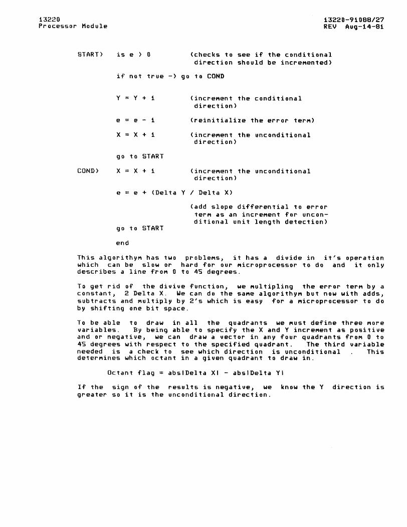
START)
COND)
is e ) 0 (checks to see if the conditional direction should be increMented)
if not true -) go to COND
y = y + 1
e = e - 1
x = X + 1
go to START
x = X + 1
(increMent the conditional direction)
(reinitialize the error terM)
(increMent the unconditional direction)
(increMent the unconditional direction)
e = e + (Delta Y / Delta X)
go to START
end
(add slope differential to error terM as an increMent for unconditional unit length detection)
This algorithYM has two probleMs~ it has a divide in it's operation which can be slow or hard for our Microprocessor to do and it only describes a line frOM 0 to 4S degrees.
To get rid of the divive function~ we Multipling the error terM by a constant~ 2 Delta X. We can do the saMe algorithYM but now with adds~ subtracts and Multiply by 2's which is easy for a Microprocessor to do by shifting one bit space.
To be able to draw in all the quadrants we Must define three More variables. By being able to specify the X and Y increMent as positive and or negative, we can draw a vector in any four quadrants frOM 0 to 45 degrees with respect to the specified quadrant. The third variable needed is a check to see which direction is unconditional This deterMines which octant in a given quadrant to draw in.
Octant flag = abslDelta XI - abslDelta YI
If the sign of the results is negative~ we know the Y direction is greater so it is the unconditional direction.

13220 Processor Module
13220-91088/28 REV Aug-14-B1
The vector length or the nUMber of dots to be drawn is deterMined by the unconditional direction's value. Since it is this direction that is increMented every iteration, the integer value of the Delta will be it's length.
The resulting algorithYM is the one that is used. flow chart figure 3.0.
Note: The error terMS are now called discriMinants.
START) is OCTANT FLAG < 0 yes, then increMent Y with Yinc no , then increMent X with Xinc
is DISCRIMINANT < 0 yes, then increMent DISCRIMINANT WITH D1
GO TO START no , then increMent DISCRIMINANT with D2
Please refer to the
and increMent the conditional direction with it's increMent GO TO START
D1 and D2 are increMental discriMinants used for slope detection and error terM reinitialization, respectively. Initial DiscriMinant = -I Delta X I + 2 1 Delta Y
Dl = 2 1 Delta Y I D2 = 2 I Delta Y 1 - 2 I Delta X I

13220 P,'oe:essor Module
13t?20 -"9 j. OBB/2(~ REV Aug-14-"81
3.4 .. 2 Graphics 1/0 allocations
-_ .... _---_ .. _---------------------------_ .. ---------_ ..... -----1/0 PORT 1 DE.SCRIPTION
, ADDRESS (HEX)' I~=============~========================================
CD
:::::::;::::::::::=:::::.:-.:::::::::::::::::::::
C1
_ ......... _._ ......... -._. __ ._ ........ . .... -. _. _. -. -' _. -....... -. _. _. _.-C2
Write to static raM- Y starting address (LSB)
Write to static raM- Y starting address (MSN)
======================================== Write to static raM- X starting address
(LSI! ) ============== ========================================
C3 Write to static raM- X starting address (MSN)
============== ========================================, C4 I Write to static raM- Dot count (LSB)
==============1======================================== CS , Write to static raM- Dot count (MSN)
==============1======================================== C6 I Write to static raM- Initial Dese:riMi-
, nant (LSB) ==============1========================================
C7 1 Write to static raM- Initial DescriMi-1 nant (MSN)
1==============1======================================== C8 Write to static raM- IncreMent D1 (LSB) .... _ .................. _ .... __ ._._ .... -_. _ ...... _ ......... _. -. _. _. _. _. _._. = :::: =::::::::::::::::::::::: =:::::::::: :::: ==: =:::: = =:::::::: =: =::: =:= == =::::::::: == =:::: = = C9 Write to static raM- IncreMent D1 (MSN)
============== ======================================== CA Write to static raM- IncreMent D2 (LSB)
============== ======================================== CB Write to static raM- IncreMent D2 (MSN)
CC Write to static raM- Yinc (LSB) - _ ......... _ ••••• _ ......... _o. •• - ........ _ .. . _. _. -'-'-' _._.-. -- _. _. -_._. ========================================
CD Write to static raM- Vine: (MSN)
ontinued ....

13220 Processor Module
13220-91088/30 REV Aug-'14-81
,0'1/0 f) OR T ----.. --... -,---.. ----
1 ADDRESS (HEX) 1 ----------------
l===========================~===========================
I I I 1 I 1 I I I I I I I I
CE 1 Write to static raM- Xinc (LSB) ==============1========================================
CF 1 Write to static raM- Xinc (MSN) ==============1========================================
DO 1 Write to static raM- not used ==============1========================================
Dl Write to static'raM- Octant Flag (MSN) ============== ========================================
DA Write to static raM- OOH Test constant (LSIO
DB Write to static raM- XEH Test constant (MSN)
============== ======================================== DC Write to static raM- OtH Test increMent
(LSB) ============== ========================================
DD Write to static raM- XOH Test increMent (MSN)
==============1======================================== DE
..... -. __ ..... -- ........ '-'-'-'-'---_. __ ..... __ .. _._._.- - _ ..... DF
=: =: =::::::::::::::::::::=:~:::: =: :..;:: = El
Write to slatic raM- OOH Copy constant (LSB)
======================================== Write to static raM- XOH Copy constant
(MSN) ======================================== Write regis~er- Modes and Prescale
7
MSB
Bi ts ()-'3 > Bits 4 and
s
Bt t 6 > Sf~t Bit 7 > s.et
4 3 1 ()
LSB
Prescale 1'5 cOMpliMent S > Mode
OOB clear Mode OtB set Mode lOB cOMpliMent Mode ltB jaM Mode
to Blank Video to inhibit l'st dot write
1::::::::::::=:::::::==::::::::=:::::::::::: ======================================== continued ...

13220 Processor Module
13220-91088/31 REV Aug-14-81
3.4.3
========================================================~ , lID PORT I ADDRESS (HEX) ,==~=======~=== I E2 I I , I I 1============== I E4 1 I 1 ,====~=====~=== 1 E8 , I I I 1============== 1 FO I 1============== 1 Fl I
DESCRIPTION
======================================== Read Status- Graphics controller
status
Bit 7 ) Busy Flag Bit 0 ) Vertical Blank tiMe
(write to clear) ========================================
Write to Pattern Register-writes a bit pattern to the pattern register and also sets scale of the pattern.
======================================== Write Drawing Flags-
Bit 7 ) set to Draw Vector Bit 1 ) low to set or clear
MeMory Bit 0 ) low to inhibit pattern
======================================== Read Vector Data-reads MSB of specified
Graphics Word ========================================
Read Vector Data-reads LSB of specified Graphics Word
=========================================================
Graphics Controller and ALU
The Graphics Controller and ALU are responsible for receiving and executing vector paraMeters downloaded by the ZaOA. Before a vector can be written into graphics MeMory, the ZaOA, knowing X and Y start and end points, Must calculate the dot count, descriMinants, Mode and etc. which describes the vector fully. These paraMeter are then downloaded through the graphics bus transceiver, U410, to the proper address locations in raM (U21, U33, and US3). The address of these raMS are Multiplexed by US2 and selects between the ZBOA addresses or the graphics controller addresses. When the graphics controller is not busy it allow the ZaOA the address the raMS. The port decoding is done with U82 and U71 Monitoring addresses CO thru FF and the NIO request signal to enable the various ports in the graphics liD.
After downloading the vector paraMeters to the raM (address locations CO through DF), the ZaOA writes to port E1 to set the Mode and scale. Port El is decoded by U94 pin a and the data is latched by U49. See Graphics lID allocation for bit assignMent of this port.

13220 Processor Module
13220-91088/32 REV Aug-14-B1
If the vector is to be drawn with pattern, a write to port E4 will load pattern and scale (previously defined at port El) into the shift register U4B.
While all the paraMeter are being set up by the ZaOA, the ProM Based Microsequenced Graphics Contl'oller is in a wait loop waiting for the Z80A to set the draw bit telling it to go ahead and draw the vector.
The internal bus is 16 bits wide of which the lower byte ROR7-RORO, contains ALU raM addresses or prograM JUMP locations and the upper byte ROR1S-ROR8, containing the ALU intructions. The instructions are decoded by U41 into siMple add, store and JUMP signals.
This architecture is basically pipelined having the prograM counters U31 and U32 address the two prograM proMs U42 and U22 clocking the instructions and address locations to two octal latches U23 and U43.
A~ter the ZaOA done sending vector paraMeters it writes to port E8 which consists of three d flip-flops USl, and U61, setting the draw bit to a 1.
The controller is Monitoring this bit through the deMux U62, while it is . in it's wait loop. Upon receiving this bit the prograM counters, U31 and U32, begin to step through the Micro code of the proMs. The proM code then executes the vector algorithYM described in section 3.4.1.

13r:.!;~0 Processor Module
13220-91088/33 REV Aug-·j.4-81
PON
WAIT
DlOOP
DOTC
The proMs, U22 and U42, are 32 X 8 bits and contain the following Micro-code:
pr~OGRAM
ADDRESS INSTRUCTION CODE (U4~:.!)
ADI>r~ESS (U22)
OPERATION
============================================================ OOH 60H OOH
==========1=============1========= niH 02H 1 niH
Power On, Flag resets controller into wait 1 =======================1 JUMp NOT BUSY,to WAIT
========== =============1========= ======================= 02H 84H 1 OOH load YaddrB } YaddrA
========== =============1========= ======================= 03H 841-1 1 11H load XaddrB } XaddrA
========== =============1========= ======================= 04H 84H 1 22H load Dote B ) DotC A
========== =============1========= ======================= OSH 841-1 ':~3H load InDiscB )
========== =============1========= ======================= 06H 841-1 1 881-1 Iload OctFgB ) OctFgA
========== =============1========= ======================= 07H 88H 1 I>1H Test Carry Xaddr, OvfI0
========== =============1========= ======================= , OSH 03H 1 ODH JUMp on Carry to DOTC 1 ==:::=::::::::::=:::= =============1========= ======================= 1 09H 88H 1 DOH Test Carry Yaddr, Ovf'lo 1 ::::=:::==::::::=== =============1========= ======================= I OAH n:~H ODH 1========== ============= 1 OBH 1 20H 1==========1============= lOtH 1 40H 1==========1============= 1 ODH , 80H 1==========1============= I OEH 1 O:~H
1==========1============= 1 OFH 1 8SH 1==========1============= continued .....
==:=::::::::::==== 01H
:::::::::::::=:::::.'"::==
() OI-l :=::::::::::::::::::::::=
E2H ::::::::::::=:==:::::
OOH _._._.-.-._ .... _-_._._.-. __ .... _-F'8H _._._-._. __ .-._.-._._._ ... - ..... -
,JUMp on Carr' y to DOTe
Store X address ======================= Store Y address ======================= Add to DotC, incr'eMen t ======================= JUMp on Carry to PON ======================= Test sign of' OctF'g ----------------------------------------------

1:3220 Proces!:ior' Module
13220-91088/34 REV Aug-14-81
YUNe
DOD
PROGRAM ADDr~ESS
INSTRUCTION CODE (U42)
AI)l)RESS (U22)
OPERATION
===::::====::::======::::=======::::=~=::::====::::::::::::::::=============::::=====::::====
10H =: =:=::::: =: =: =::.::::::: ==
iiH ::: =:::::: =:::::::::::: =:::::
i2H =::: =: ::=:::::::::::::::::
01H :: =::::::::::: = :::::::: =:::: =
BOH _. -_._.-. - .... _. ' ... _._. -"_. _. _. _. _. _. -' _. _. -' _. _._. OOH
:::::: =: =:::: =::::::::::: =: :~::::::::
80H
13H IJUMp Sign neg. to YUNC ::::=:::. :::::::::::::::: :;::= 1 ::::::::=:::: =:::::::::::::::=::::::::::::::::::: :::::::: ::::;::::-.: ::::::::::::
71H IAdd to Xaddr, Xine :::::::::::::::::::: :::::::::::::::: 1 :::: ::::::::::: :::::::::::::::::::::::::::::::::::::::::::::::::::::::::::::::::::::::::::
14H IUncond JUMp to DOD =:::::::: ==:::::::: ~::::: 1 ::: ::::::::::: =::::::: :::::::::::= :::::::::::::;:::::: :::::::::::::: :'.:: ::::::::
60H IAdd to Yaddr, Vine =::::::::::::::::=:::::::::::= =:::==::::===:::=:::== ====:::=::::::::::: ::::::::===::::====::::::::::::::=:::::::::::::::==:::::::
i4H BSH F3H Test DescriMinant ( 0 ::::::::=::::=::::::::=::::::: ===:::::::::::::::=::::===:::: ==:;::===::::=:::: ===::::=====::::======::::==:::===
iSH OiH iDH JUMp Sign neg. to DODI =======::::== ::::===:::::::==::::==::::::::1==::::::::===:::::::: =========::::::::=======:::==::::=
16H BOH 1 S3H Add to DescriMinant, D2 :::::::::::===::::=:::::::: ::::::::::::===::::=::::===::::1======:::::::::::: =========::::::::====::::======= '17H BSH 'F'BH Test sign of ()etF'g 1====:::::::::::::::::::::::: ::::::::::::=::::::::::::=::::===::::1==::::===:::::::::::: ==::::::::::::::::=:::::::::::::::::::::::::;::::::::::::::::::::::==:::::::: 1 iSH 01H 1 iBH JUMp sign neg. to YUNC2 1::::::::=======:::: ===::::::::=====::::==1==::::::::=::::==:::: ===========::::====::::====== 1 19H SOH 1 60H Add to Yaddr, Vine 1::::::::::::==::::=::::=:::: ==::::::::::::==::::====::::1::::=::::====== ======~================ 1 1AH OOH I 07H Uncond JUMp to DLOOP I==::::~====== =====::::=::::=====1========:::: =====::::==::::==========::::===
YUNC2 \ lBH SOH 1 71H 1 Add Xaddr, Xinc 1========== ========::::====1::::========1======================= \ 1CH OOH 1 07H IUncond JUMp to DLOOP 1 1==========1============::::1=========1==========::::========::::===1
DODi 1 lDH 1 SOH 1 43H IAdd to DescriMinant, Dl1 \==========1=============1=========1=================::::====::::1 1 1EH 1 OOH 1 07H IUncond JUMp to DLOOP 1 1==========1=============1=========1=======::::===============1 1 1 FH I XXH 1 XXH 1 not U ~!)ed 1 ============::::===============================================

13220 Prucessur Mudule
13220-91088/35 REV Aug-14-81
The Graphics controller steps through the Micro-code and uses the ALU tu check fur Carry and Sign Bit for conditional JUMpS. Referencing the Micro-code the first operation done is to download the starting Y address, starting X address t Dot Count, Initial DescriMinant, and the Octant Flag. This is copied to the saMe address locations froM register B (U21, U33, U53) tu register A (U64, U44, U24). By doing this we can use register A as the update register, and register B for the increMental value to be added to register A.
The next step is to check to see if both the X and Y starting addresses are within the write address range of ther graphics MeMory. This is done by addressing the X or Y address frOM register A and adding it to the overflow constant EOOH frOM register B. ReMeMber that the ALU only has 12 bit resolution and we are checking to see if the X or Y value is larger than 512B (9 bits). By adding EOOH to it and getting a carry, we know it is out of the addresable space of the MeMory. The additions are done thruugh 3 4-bit full adders (U54, U34, U14) and are latched by 3 4-bit latches (USS, U3S, U1S) using the inverted outputs. This is done because the raM outputs and operation of the ALU is cOMpliMented. The Carry and Sign bits are latched by U63, a D flip-flop.
The controller then increMents the dot count and checks to see if it is done drawing the vector. In this algorithYM the dot count deterMines the vector length.
The next step is to test the Octant Flag to see which direction is uncunditional.
The unconditional direction is then increMented and then the DescriMinant is checked fur sign. If negative, the prograM JUMps to an instruction to add the increMental DescriMinant D1 to the exsisting DescriMinant then JUMps back to the X and Y overflow check at the begining and starts the algorithYM allover again. If the sign is positive then it knows to increMent the conditional direction. The addition of the increMental DescriMinant D2, to the exsisting DescriMinant is dune. An unconditional JUMP back to the overflow check is then executed.
All JUMps, conditional or unconditional, is done by preloading the prograM address counters U31 and U32 with the JUMP location if the conditions are Met. If a JUMP occurs, the instruction decoder Must be inhibited frOM exec.uting a false instruc.tion (this is because it take two clocks to execute an instruction>. US1 inhibits an instruction cycle by Monitoring U62 pin 7 for a JUMP load signal.

13220 Processor Module
13220-91088/36 REV Aug-14-B1
4.5.1
After each iteration thr~ugh the prograM loop, if the X and Y addresses are valid, they will be stored in teMporary re~isters U25, U45, and U6S. Both the X and the Y addresses are 9 bits in length. Upon storage of the Y address a dot request flag is set in hardware to tell the write state Machine a valid dot address was cacu1ated. U67 sets this dot request. The state Machine U75, is responsible for getting the dot written into the display MeMory at the address specified by the dot address of the ALU. The ALU addresses the display MeMory as follows:
X addr (U25+U65) Y addr (U4S+U65) =================== ===================
S) 1011121314151617181 S) 1011121314151617181
I--**---I----word address of bit location-----I
** = bit in the word location to be written to.
Note: Each word is 16 bits so the lower 4 bits of the ALU X address is used to select the coresponding bit in that word.
The Word address is then Multiplexed and used to address all 16 dynaMiC raM in the display MeMory of the specific word location in which one of it's 16 bit is to be written to.
The Multiplexors U26 and U46 Multiplex the word address of the ALU.
This cOMpletes the description of the priMary functions of the Graphics Controller and ALU.
GRAPHICS DISPLAY AND MEMORY
The display circuitry is responsible for the accessing of graphics MeMory for raster scan video iMforMation. The display hardware consists of a RAS, MUX, and CAS generator for the graphics raM, display counters, display MeMory (16K X 16), and display related hardware sync circuitry.
Graphics Dot Clock Syncronization
The display resolution of the graphics is 512 X 390. If we use the saMe dot frequency of the alphanuMerics (25.77 MHz), the graphics display would occupy a sMall portion of active video. Also the scaler aspect ratio would be off. By dividing the 25.77 MHz clock down 1.S tiMes, we will have a 17.181 Mhz graphics clock.
13220 Processor Module
13220-91088/37 REV Aug-14-81
4.5.2
For every three alpha dots in the X direction, you will have two dots of graphics. This also Made it posible to have a correct aspect ratio with respect to the dot resolution.
By using two tiMe shifted divive by three 16.66% duty cycle clocks (U97, U89, US?, U98) we can "or" the two together and forM a 17.181 MHz 33.33% duty cycle graphics clock. U8B "or's" these two signal together and forMs G elk.
The 2/3 clock or 1 1/2 divider is created in hardware by a D flip-flop (U89) and 4 bit syncronous counter (U97).
Reference figure 12.0 Graphics Dot Syncronization.
On the first NlCGAX signal, the counter U97 loads a binary 7 into it registers on the positive edge of DRCX, the 25.77 MHz dot clock. On the next negative edge of DRCX U89 is Clocked. What is clocked through is the signal on U97.14 which is a 0, which Makes U89.6 a "1" since the output is off of Q NOT. This set up US? for the next rising edge of DRCX when US7 will output a 1 for the 19.4 nS high tiMe of DRCX. On
the next negative edge of DRCX, U89.6 is clocked low disabling U87 until the 4 clock edges where this is repeated. This is on of the two 1/3 dividers. On the following positive edge after U89.6 goes low, U97.11 goes low enabling U98 for the next negative edge of DRCX when another 19.4 nS high tiMe frOM U98.1 will occur. On the next rising edge U97.11 goes high disabling U98. U98 generate the second 1/3 divider only tiMe shifted by 38.8 nS (one DRCX tiMe). These two clocks are then "or'd" by U88 to forM the graphics dot rate clock G ClK.
Graphics Display
The display MeMory is bit-Mapped and is accessed 16 bits at a tiMe (words). Each sixteen bits constitutes a graphics word. Therefore the display raster consists of 32 words by 390 lines of graphics dot iMforMation. (32 words X 16 bits = 512 dots in the X direction.)

13;.?20 Processor Module
13220-91088/38 REV AUG-14-'81
line o 1
3B9
1------------------- 512 dots -------------------1
word 0 ,............. . .............. 1 word 32
word 0 I ............................. 1 word 32
The display counter U17, US7, USb, U37, and U47 are used for addressing the graphics raM for every word access. At Start of FraMe when all the counters are reset signifing the top of screen scan for the first line of video, a raM access of the first word of the first line of video is done.
The word address is increMented for the next word address of the first scan line which another word access is done for shifting out continuously with the previous word as video graphics data.
The counters are clocked and another word access is done. This is repeated for every scan line until the hardware receives another Start of FraMe signal which occurs every fraMe tiMe.
Addressing consist of 14 bits in which the lower S bits are the Word count and the reMaining 9 bits are the line count. As in the AlU addressing, this is Mutiplexed by U36 and U16 for display accesses. Since the address counters are syncronously increMented, each address tells which word is being fetched.
"----line 0 Iword 0 Iword 1 I ..... word 32 1 address OOoooooonooooo 00000000000001 000000000111111
----~----'"--------line 1 1 word 0 1 word 1 I ..... word 3;,? 1 address 00000000100000 00000000100001 000000001111111
-----"-"-~---
The reference clock called DIS eye is a clock divided by 16 frOM the G elK (graphics dot clock 17.181 MHz). This clock is frOM U76.11.
U76, U77, U78, U79 control the ras, MUX and cas signals for display writes or reads into graphics MeMory.

13220 Processor Module
13220-91088/39 REV AUG-14-81
Reference figure 11.0 for display MeMory tiMing.
When the DIS eyc clock is low for B G elK cycles the display hardware allows a ras, MUX and cas for a display word fetch at the address on the display counters U17, US7, US6, U37 and U47.
The U29) word
signal DlOD frOM U710.6 loads the two 8 bit shiftregister (U19, of the word accessed. On the next G elK the first bit of that
is shifted out as serial graphics video to the video Multiplexor.
Display Counters
The Rowand ColUMn address control is done by u~ing a 4 bit counter U76 as a reference. After a Start of fraMe, U76, which is clocked by G elK, starts to Up count. The lower three bit are used to select the deMultiplexor U77 which controls the D flip-flops U7B and U79 which create the GNRAS, GMUX, and GCAS.
The fourth bit is the divide by 16 signal that is referenced as DIS CYC. So for every 16 G ClK's, or dot tiMes, we can have two ras and cas cycles of graphics MeMory. Since one display word fetch is 16 bits long and it only takes 8 dot tiMes to access and latch the word, the reMaining 8 dot tiMes for which another ras and cas cycle can be done is allocated for MeMory writes, since during this tiMe we are still shifting out the 16 bits as video iMforMation.
At the end of the count (16) the carry bit U7b.1S enables the word counters U17 and US? which is c.locked to the next word address of that display scan line. There is only one ras and cas cycle per 16 dot tiMes for display accesses and only one ras and cas cycle per 16 dot tiMes for MeMory writes during one DIS eye period. The MeMory cycle for writes is controled by the Write State Machine which enables the ras and cas generator U77 during the second 8 dot tiMes of the DIS eye signal.
See Write State Machine section 4.5.7.
After every 16 dot tiMes or G elK's the Word counters are clocked. At word 31 (the 32'nd Word) US6 the J-K flip-flop toggles and a binary 21 (for word 21) is preloaded into the word counters U17 and US7. This will count to word 31 again for horizontal retrace tiMe which is 11 word tiMes. A two dot tiMe delay is needed to sync with the analog sweep frequency. This is iMpleMented by Ubb a 4bit shift register. It delays U7b frOM counting for two dot tiMes at the end of every line. Also during retrace the ras and cas for display addressing is inhibited by U88.1,2 being both low at this tiMe. At the end of Word 31 of retrace, USb.S toggles high and clocks the line counters U37, U47 and USb to the next line address.
The signal GBlANK goes active high during retrace and inhibits loading of the video shift registers. This is repeated every scan line until another Start of FraMe signal COMes again.

j.3220 Pr'oce~:;sor Module
13220-91088/40 REV Aug-14-81
4.S.3 Start of FraMe
The Start of FraMe (SOF) signal is responsible for syncing the graphics display to the character display of the terMinal. It's two Main functions are reseting the display counter when the scan line is at the top of the screen and to start the graphics video sixteen graphics dot tiMes before start of charact(~r video. Since the graphics dot tiMe is 2/3 that of the character dot tiMe 1 480 graphics dots will occupy 720 character dots on the saMe line of video.
(720 character dots X 2/3 = 480 graphics dots)
If we have 512 graphics dots per scan line 1 there will be a 32 graphics dot overlap on top of the character display. To SYMMetrically center the two 1 the SOF Must tell the display circuitry to start the graphics video 16 graphics dot tiMes (or one word tiMe) before character data appears on the screen. This will leave 16 graphics dots after the character data has ended Making the graphics centered with the character display.
I I I I I---------Character Display----------------I (720 dots @ 25.77 MHz)
I I I----I---------Graphics Display-----------------I I (S12 dots @ 17.1B1 MHz) I I I I I I I I , I
I I
The operation of SOF is explained as follows: In both SO and 60 Hz operation 1 Vsync goes active low during vertical retrace and goes inactive high 6 scan lines before the first line of video (7th line).
Counter U810 is the SOF line counter which is clocked by LRCX 1 line rate clock. As NVSYNC goes low line counter US10 preloads 9H into it's registers. When 9H preloads on the nexted clock frOM LRCX 1 Qd (UBtO.11) is set to a 1. As NVSYNC goes high the P and T inputs to U810 are enabled by U87.6 going high. The counter then counts the next 6 LRCX clocks which on the 6th a carry wiil appear on U810.1S. This is an enable signal to the character counter U89 and U99. The character counters are held off until horizontal retrace tiMe. This is when NLRCX is high. To start the graphics video at the right tiMe 1 SOFC (U99.1S) Must occur two character dot tiMes into the -S character pOSition of the first line of video.
Reference figure 13.0 Start of FraMe TiMing.

13220 Processor Module
13220-91088/41 REV Aug-14-S1
4.5.4
After U89 and U99 count 30 character tiMes in retrace on the 30th clock SOFC (U99.1S) goes active. U89 and U99 are clocked by NlCGAX which ~s the the character rate clock. SOFe signal is clocked through to U79.8 as SOF by the SOF elK (U91.12). SOF resets not only the display counters but also the the SOF circuitry itself. When SOF occurs U810 is asyncronously reseted causing US10.ll low which disables the P and T inputs of U810.
This disables the carry (U810.1S) which disables the T input to U99 which in turn disables the SOFC signal. This all occurs before the next SOF elK so on the preceeding SOF eLK the SOF signal will go inactive. The graphics hardware takes 10 graphics dot tiMes to fetch and load the video shift registers (U19 , U29) before the the first video bit is shifted out. This puts the graphics video bit 24 character dot tiMes before the first character or 16 graphics dot tiMes (24 X 2/3 = 16 graphics dot tiMes).
Since each graphics line is syncronous with each character line , SOF only occur at each fraMe interval.
Graphics Drawing Modes
There are for drawing Modes iMpliMented in the hardware. They are:
CLEAR MODE: Writes 0'5 into MeMory along the vector path.
SET MODE: Writes l's into MeMory along the vector path.
COMPLIMENT MODE: COMpliMents the MeMory along the vector path.
JAM-PATTERN MODE: Writes the pattern data into MeMory along the vector path.
The bits MODEO and MODEl frOM the latch U49 select what Mode in which the vector is to be drawn. The graphics raM data deMultiplexor US10 , selects what is to be written into the graphics raM frOM what these two control bits are set to.
MODEl MODEO Mode ----- ----- ------
0 0 CLEAR 0 1 SET 1 0 COMPLIMENT 1 1 JAM-PATTERN

13220 Processor Module
13220-91088/42 REV Aug-14-81
4.5.5 Scaled and Pattern Drawing
The scale register (U59) and pattern register (U48) controls the way all data is written into graphics MeMory in all four Modes. In the first three Modes, clear, iet and cOMpliMent, the pattern register is used as a write Mask by controling the WRITE CONTROL signal with the pattern data through usa. When it is in jaM-pattern Mode, the pattern register is used as the actaul data to be written into the graphics raM.
The scale register (US9) controls when the data in the pattern register is clocked out. A sMall exaMple on how this works can be shown as follows:
Let's define, as the Z80A would, a scale of 2, and a pattern of SSH. Upon writting SSH to port E4 the pattern register, the scale value is also preloaded into US9. ~or a scale of 2, a 1110 binary would be preloaded.
SCALE = 1'5 COMpliMent of (scale - 1)
In this exaMple scale = 2-1 = 1, the 1's COMpliMent of 1 in four bits is 1110B. If it was 4, scale = 4-1 = 3, 1's COMpliMent is 1100B.
The Write State Machine, ex~lained in section 4.5.7, clocks the scale and pattern registers on every dot MeMory cycle. With the scale set at 2, and the pattern set with SSH, the first dot written into raM will be a "1" since in the pattern SSH the first bit is a "1".
pattern register
I 0 I 1 I 0 I 1 I 0 I 1 I 0 I 1 I )data shifted --------------------------------- out
The Write State Machine will clock the scale register but not the pattern register becau~e the carry bit froM US9.1S not being set keeps the pattern register froM clocking. Now the carry bit US9.1S is set to a "1" froM the increMented preloaded count of 1110B to ll11B.
On the next dot write the pattern register still has a "1" on the output and this will be written again into the graphics raM. The scale register now allows the pattern register to clock to the next data bit which is a "0". The previous "1" is recirculated back into the last bit position. At the saMe tiMe the pattern register is clocked, the scale is again preloaded back into the scale register US9 and this is repeated until the vector path drawn is COMpleted.
By having a scale of 2, we delay the shifting of the pattern register by 2 dot write into MeMory Making the pattern drawn twice per bit giving the effect of Making the pattern twice as large.
ReMeMber this is used both as a write Mask and data depending on which Mode you are in.

13220 Processor Module
13220-91088/43 REV Aug-14-B1
4.5.6 Display Write State Machine
The priMary function of the Write State Machine (U7S) is to execute, upon receiving a DOT REQ, a write sequence into graphics MeMory the correct dot data of the vector that is currently being drawn. It is also responsible for the current scale and pattern data of that vector.
Reference figures 9.0 and 11.0.
Upon receiving a DOT REQ froM the ALU the Write State Machine, which is clocked by DIS eye, clocks the request through on the first negative edge of DIS eye. A this tiMe a display word fetch for screen refresh is executed and takes up the next 8 graphics dot tiMes. On the rising edge of DIS eye, M DOT goes low (U8S.3) since the DOT REQ was clocked through to U7S.S. M DOT is the signal that enables the GNRAS and GNCAS signals during a MeMory read-write tiMe (a MeMory read-write tiMe is when the DIS eye clock is high for 8 graphics dot tiMes) and uses the ALU adresses to read or write dot iMforMation of the graphics raM. M DOT enable a raM access by allowing U86.3 to be high and enabling U77 to do a GNRAS and GNCAS when the DIS eye signal is high.
A word access is then done using the dot address of the ALU. When the word becoMes valid, all 16 bits of that word is latched into to 8 bit latches U28 and U1a by the signal NALOD.
By latching the word location in which the actual dot address is at we can now Modify it, in the case of cOMpliMent Mode, by addressing the actual bit we are looking at. This is done by using the lower 4 bit of the ALU X address DBITO-DBIT3. Using a deMultiplexor with a cOMpliMented output (U39), the bit that is to be cOMpliMented is selected and feed back to UStO the graphics raM data deMultiplexor as the cOMpliMented data to be written back into the graphics raM at the saMe ALU address location on the next MeMory cycle.
NOTE: This reading and latching of the word at the ALU dot address is not necessary for clear, set, or jaM-pattern Modes since the dot data is or has been predefined. The hardware does it anyway.
This cOMplete the first part of two MeMory cycles that occur for every DOT REQ forM the ALU.
After the MeMor'y read cycle is done, DIS eye goes low and a display MeMory word fetch for the next display word on the current scan line is executed. What also occurs is the clocking of the Write State Machine. This Makes GNWRITE (U7S.7) go low which disables the clocking of the word latches (Ut8, U28) through U83 and enables the graphics raM write selector U310. U6tO.8 which is low, because DIS eye is low, will enable U310 when DIS eye goes high again for the MeMory write cycle tiMe.

13220 Processor Module
13220-91088/44 REV Aug-14-81
4.5.7
4.5.8
When this occurs U310 selects 1 of t~e 8 write lines to both banks of graphics raM. DBITO-DBIT2 select which one of 8 raMS are written to, and DBIT3 controls which bank of 8 (Ull0-Ul17 or U210-U217) gets the GNRAS and GNCAS strobe signals. This allows only one bit of the word address specified by the ALU address to be written too. The raM data could have been 0 (clear), 1 (set) cOMpliMented (data latched and cOMpliMented through U39.6), or pattern froM the pattern shift register U48.
The negative edge of the current DIS eyC signal will clear the Write State Machine and leave it idle until another DOT REQ COMes. Also the pattern register (U48) (if allowed) and the scale counter (S9) is clocked. This sets up the hardware for the next DOT REQ.
The Write State Machine after receiving a DOT REQ executes a read and write cycle faster than the ALU can calculate a new dot address. Therefore there is no handshaking with the ALU.
Also occuring at the end of the write cycle is a signal generated frOM U77.7 that goes through U83.6 to create a signal called DOT CLR. This clears the DOT REQ latch U67.
l's Dot Inhibit
The purpose of this hardware feature is to inhibit the first MeMory write of the vector being drawn. Since the first dot address of the current vector is the last address written to frOM the previous vector Makes the first pixel position has already been written.
As an exaMple, if we were in COMpliMent Mode, the first bit of every vector in a chain would be recoMpliMented. By inhibiting the first dot write, the first bit in every vector would only be COMpliMented once.
The l's Dot Inhibit bit is latched frOM a ZaOA port write to U67. After the Write State Machine (U7S) COMpletes the first read and write cycle the signal DOT CLR is generated. This clears the l's Dot Inhibit latch so the reMaining dot writes are not inhibited.
Graphics Raster DUMP
The ZaOA can indirectly access the graphics MeMory to retreive video word iMforMation to dUMP to the internal dot printer. To aCCOMplish this without disturbing the existing MeMory we use the l's Dot Inhibit feature.
By writing a 1 dot vector to any 16 dots of the word location wanted and setting the l's Dot Inhibit on the ALU gives only one DOT REQ at the specified address but is inhibited by the hardware l's Dot Inhibit leaving the graphics MeMory unchanged. What we aCCOMplished was to latch the word in U18 and U2a which can be read back by the Z80A through port assignMents FO and Fl (hex).

13220 Processor Module
13220-91088/45 REV Aug-14-81
The Z80A reads 15 words in the Y direction and sends 1S bytes of the word to the printer after buffering the reMaining 1S bytes. Then this is sent to the printer to be printed. The X direction is increMented 16 and 1S More words in the Y direction are read. This is continued until all display words are read and printed. This is all done by writing 1 clot vectors then reading theM back froM the graphics hardware.

13220 Pr oceS501' Modu Ie
13220-91088/46 REV Aug-14-81
S.O Glossary of Signal NaMes
This section lists the signal naMes used on the scheMatic drawings, figures 21.0 to 24.0, along with a brief description of their use. Note: an 'N' prefix gen£~rally indicates an active low signal, otherwise the signal is active highj a 'T' prefix or an 'X' suffix indicate that the signal is buffered.
1.84 MHZ
3.68 MHZ
60 HZ
ADD
ADDR COUNT
AL.PHA
BATT ... or BATT···
BEL.L
BIA 0-3
BL.ANK
BL.INKRATE
CE
CL.RSTMEM
( 'C:' , ... >
eTR eL.K
The 1.84 MHz datacoMM chip clock
The 3.68 MHz Z80A clock
Sets the video fraMe rate, low ~ SO Hz
signal used to latched output of adder in the graphics ALU
enables the word counters in the graphics display circuitry. video dot streaM after dot stretch
connection to the hatter'y + (or -) terMini:ll. for CMOS backup during 'power off
output signal to drive the keyboard bell
buffered internal ALU address to the ALU static: raM.
inhibits the ALPHA dot streaM froM being sent to the sweep circuitry
alternates at the blinkrate for blinking character attribute carry bit in the ALU graphics hardware used for overflow checks
detects presence of loopback hood
clear or set graphics MeMory by setting Iowa write to all graphics OCC\H'S.
clear-to-send frOM host COMputer
A 4.2 MHz clock dirived frOM dividing the 17.181 MHz G eLK by 4 to run the graphics. c:nntrolel'

13;~20 Pr oceSSOl' Mod U Ie
eTS
CUR
DBITO-DBIT1'7
I>ISBRQ
DIS eye
DISD
I>l.0I>
1)01' Cl.R
1>01' INH
DOT REQ
DISPOFF
DM
DI~CX
1)SR
ENO-EN'l
ENHOFF
ENNMI
EOl.
FLAG
GBl.ANK
G eL.K
GMUX
GNCAS
TTL level clear-to-send
cursor output froM CRTC
13220-91088/47 REV Aug-14-··S1
ALU addressing bits after being latched
inhibit DMA
A divide by 16 reference froM G eLK for display tiMing purposes
the inverse of the DIS eye clock
display load signal to the graphics video shift registers
clears the DOT REQ after a MeMory cycle of the graphics raM is COMpleted
1's dot inhibit signal set in hardware
dot request froM the ALU telling the hardware a valid dot address is ready
blank entire display
detect ModeM connection
dot rate clock
TTL level detect ModeM connection
enhanceMent data bits froM line buffer
inhibit enhanceMents
clock for NMI Mask latch
graphics end of line
signal to reset graphics controler
graphics horizontal blank signal
17.181 MHz graphics dot clock
select signal to change frOM row to colUMn address of the graphics raM
graphics colUMn address strobe
13~?20 Pr oC~~S)SOl\ Mod u Ie
GNRAS
GNWRITE
GVIDEO
GWI~ITE
HBLANl<
ICH
11)0,-11),7
INVERSE
JUMP
KEYO-·KEYb
LHCDEL
LBCX
LCGADEL
LCGAX
LDO-LD'7
LOAD C
LVSRX
MI> O-'MD'7
MEMO· .. ·MEM6
MODEl)'-MODE1 MUX
NBLINK
NBUSr~E(~
NCAS
graphics row address strobe
graphics clock fur scale and pattern registers
graphics serial video data
pre-enables the graphics write decoder
horizontal blank signal
TTL level detect datacoMM test hood
13t.~20-91 088/48 REV Aug-14-f.l1
interal data bus for graphics subsysteM
select inverse video attribute
ALU hardware signal for a JUMP instruction to anothe~ address location
keyboard row/coluMn scan outputs
delayed line buffer clock
line buffer clock
delayed latch character generator address
latch character generator address
latched graphics video data
data for graphics word counters
load video shift register
RAM d a t a () u t put ~J
graphics raM address lines
graphics Mode select bits selects between row and clouMn address for d ynaMi.c r~AM
select bl1nk attribute
l'equest bus control for DMA
coluMn address strobe for RAM

13220 Processor Module
NCMOSREQ
NCUR
NDCLK
NURSOR
NENNMI
NEOLDEL
NFULLBRT
NHALFBRT
NHSYNC
NINT
NIOG
NKEYACT
NKEYDISP
NKEYSTAT
NLRCX
NLSB
NM1
NMODEM
NMSN
NMUX
NNMI
NPFAIL
enable CMOS for read/write
one line cursor signal
two graphics dot clock delay signal
cursor active without underline
select NMI latch
end-of-line signal
norMal intensity video output
half-intensity video output
horizontal synchronization
datacoMM interrupt
I/O enable for the graphics subsysteM
key active (depressed) on keyboard
select (clock) keyboard/display latch
enable keystatus port
line rate clock
graphics port decode to write into the LSB of the ALU static raM
ope ode fetch Machine cycle
select (clock) ModeM/display latch
graphics port decode to write into the MSN of the ALU static raM
clock RAM output latch
non-Maskable interrupt (video)
power fail signal frOM power supply
13220-91088/49 REV Aug-14-81

13220 Processor' Module
NPRINTER
NRAS
NRESETA
NRESETB
NRVI>
NBEl.DC
NSF
NBP
NBR
NBYSSTAT
oeD1
OCR1
PAT INH
PINT
PULLUP
RD RECIRC
RESET
RETRACE l.OAD
R<:' ,.)
50-511
SCl.0-SCL.3
S1)
SELDC
printer select signal
row address strobe for dynaMic RAMs
power-on reset, driver A
power-on r'eset, dr'iver B
graphics port dec~de for reading of graphics video data
datacoMM port select
graphics port decode to set flags
graphics port decode for scale preset
graphics port decode for status read
systeM status port select
opt ion ell C on t r 0 1 driver 1, d a t a co MM
optional control receiver 1, datacoMM
13220-91088/50 REV Aug-14-B1
inhibit the pclttern register in graphics
printer inter'rupt status
COMMon pullup resistor
receive data, datacoMM line buffer recirculate enable
printer reset signal
loads signal for graphics word display
graphics controler address lines
request to send, datacoMM
ALlJ added data
scale bits for the graphics hardware
send data, datacoMM
datacoMM chip select

j.3220 Processor Module
SIGN
SG
SHIEL.l>
SMEMO'-SMEMS
SOF
SOFC
STORE )(
~rl()RE y
TAU···TAi S
TF.HJSAK
T1)0-T1>:7
TNBUSAK
TNMI~EQ
TNRD
TNr~FSH
TNWR
TR
ULINE
Ul.TIME
VBl.ANK
VSYNC
WRITE CONTROL
WRITE ENABLE
XU···X'7
ZBLANI(
ZDO'-Zl)~7
13220-91088/51 REV Aug-14-81
ALU signal to check sign of the addition
signal ground, datacoMM
shield (earth) ground, datacoMM
RaMO-ROMS chip enable
graphics start of fraMe
carry bit that initates SOF
graphics instruction to store the X address
graphics instruction to store the Y address
address bits 0-1S
bus acknowledge, Z80A tristate
buffered data bus
active low bus acknowledge
Z80A MeMory request
MeMory or liD read select
dynaMic RAM refresh active
MeMory or 1/0 write select
terMinal ready, datacoMM
select underline attribute
active on scan line 13, indicates scan line for underline or cursor display
vertical blank signal
vertical synchronization signal
enables write decoder of the graphics raM
enable the write decoder to the graphics raM
character code address to character ROM
hardware flag set by the Z80A to stop graphics video frOM being displayed
Z80A dat.a bus


_ PRINTER - KEYRET _ -_ KEY SClfN -_ BELl... -_ TOHOST
Z80A
I/O DECODER
NMZ BUSREG BUSAK
v
'--t_B_U ___ FF-ER----J~ /
.... ~) ROM L ____ -=::J::T'Vfv 48 K ~PACf
I/O
i--
i---
,DATA BUS
VtzDA1A BUS ~ ~ . -c:: GRflPHICS
t.....--v SUBSYSTEM NIO -r 1-__ --1
-FROM HC15T _ DIITACCl'Jt1 I~KX/' 6RAPHICS RAM -
V.BLANK I DISPLAY CONrRCL
GRAPHICS VIDEO
i-----II;;..~ H S Y He F-----tl.~~ V5 YNC ~-.. ;...~ FULJ..,BAT J-o-____ ; ..... HAJ..FBRT
FI6URE 1.0 PROCE5jOR BLOCK DI/1GRRM
TerMinal Block DiagraM AUG-14-81 13220-91088

DitTA BUS I
CPU A~ 1-4 > f!atl. V
II DN!L5S BlJS
8 !lUi ADM.> .s TAT IC RAM f=> ~MUX
1U6/STEl! B /(j,><J2. 1: ALU IU)/)/l. RIJ/I.. +-~
Z80A WAITE. CONTROL -' t"'\ l '----T-
GRflPHICS '"' DRAW COAl7RJJJ... I
ADD£~ /H)IXESS t;i -7 ~
- ~1)5Y F/..A6 - If/CR()StavEN:£ PO!e.T SCAJ..£ tMODE. ALU
A flE6 AD!).!!. • .> STATIC RAM
~ " DECODER. 0 PATTE~ ADDR.. ROR.. , - ~ f<E6IS7ER. .A I CONTRO/J.E~ J CO-FI'
~7£R t:U1P /~ x /2., DATIi BUS
1- WRfTE. ~I... • /1\ J NIO I/O .RE.~lJCsr '" RElit; STA7lJS (PROM BAseD) -- CAR.R.Y BIT
-S/6N BIt l.. 1-' -- I
IIJ..~ fU>D£. UPDATE. In __
<~ 5ilfTUS ~ B(JSY RA6
STORe X AfX1il. ... ~LV A DDR.ESS K -
~ PORT _ V BJ..ANI<. STDRE Y ADM •• J..,qTCH t MUX ALU DC1r ~DDJi!.E.SS -~ l
.<
IILIJ II DOI?eS$ ..
........ ~
~ /VI RfISTER V <r- 6RAPHIC. I~BIT VIDEO WOR.D 16 BI1 RAM VIDEO D~T/I DUffP ~ ~r---r
V ~
DliTA t:: ~ i COl1PJ.JMENT f)~m LATCH ~ \/
~ ,.
LA7r.H CJ.,X ~ SQJIfL " -- tJt 16K x 16 WAITE - ~ 1 o.f' J6 ·WRITE-~ t--
~ 168IT VIDEO J::::> PATTERN __ PIIT7ERN C~CI< WRIT£ RE6/SrEl{ SrIlTE. MRCH. WRITE ENI1&.e. ·SEJ..E.Cr V
D/SPL~Y Rl/11 SHIFT HC6JSTlR SELECT DAm CRTC v
t sftJ.e ..... - ~ (DYNFlHIC)
J.ST DOT WRITE INHIBIT II .1' ~ !Q + j~ 411 Ri+M DFlTR MODE. Q
I1EI1 RAS CAS l~ P~SII1VX) CAS DMux.. DISPLAY
83~7 GENERtrrlJR IJDDRESS M U X V BUtNI< DOT RATE. CIJX.I< 25". '1715 MHz. .. smP..T !\ IN6RAS /\
CJ.I.- .- IlA1E CJ.oCK (I"C6AX) .. OF N6CAS / \ l ~
J..IN£ RI4TE CLOCI( (I....RC'I() ..... FRfI/'1~ ST~IQ" ()!= FRAME. (SOF) }...ON) .sHIFT /laISrER. (~ .......
VE£rlCAJ.., SYNC .. ~c~ DISPLAY COUNTERS -17.18IMHz. (6CI...I<.} V.£R.TlCAI... B/.IlNK. 6 CA.()CJ( 6 CJ..t:>CK 17.181 MJl6 . ---
FIGURE 2..0 GRAPHICS SUBSYSTEM BLOCK DIA6RAf1 Figur'e 2 Graphics Block DiagraM AUG-14-81 13220-91088

PON BUSY FLA6 RE~LOW
DOTe
DOD1
DOD
no
YUNCZ
FIGURE 3.0
YUNe
e.s
/to
6RRPHIC5 tllCROCODE fLOWCHART
Figure 3 Graphics Microcode Flow Chart AUG-14-81 13220-91088

Z80 ClK
(f) TA0-TA7 (f)
W NIO U U CL TNRD
CL ~ I/O SELECT CL 0 I- TDATA IN
TDATA OUT
------------------NCMOSREO
(f) (f) NWAIT W U U TNRD CL
(f) ZDATA IN
0 L TNWR U
ZDATA OUT
Tl T2 TW *
I I I 272 NS
I/O ADDR ~SS
I I I
I I
l
--------------- -------------- r--------------
I
l
I
I
~ AUTOMATICAllY INSERTED WAIT STATE
I
T3
ITW]
I
I
I
--------------
I
I
\
Tl
[T3J
I
X
--------------
I
J
\ L
T2
[T1]
I
" "
r--------------
I
\ ,/
FIGURE 4 a flJ Z8flJA liD TIMING
Figure 4 zaOA I/O TiMing DiagraM AUG-14-81 13220-91088

Z80 ClK
TA0-TA15
TNMREO INST
FETCH TNRD
NMI
SMEM0-SMEM5
ROM DATA
NWAIT
Tl T2
~ 272 NS
IN~TRUCTION ADDR
T3 T4 (Tt)
: REFRESH ADDR
Tt (T2)
r-------~(7I/////X VA~ID DATA YllJ~---r---------1------
· · IF STRAPPED: L. __ ... _________ ~--
-----------------------~---------------.-----~---------~--------------~--------------~---------------TA0-TAtS
TNMREO
MEMORY TNRD
READ SMEM0-SMEMS
ROM DATA
• • \ • I • X DATA ADD~ESS Xr-----------~---- . · · · ·
~------------~-------CZX~~---VA-l-I-D-D-A-T-A--~~)~------------------------
FIGURE 5.0 Z80A ROM TIMING
Figure S ZaOA ROM TiMing DiagraM AUG-14-81 13220-91088

VIPfO -1
I I
"RClC. (U5~.JO)
L.Ct>H. t U-tl+. 7)
) L.CC.A DEL 1
J (U4f4./O)
J
~ J""K ~ (US"I4't.'l..)
r' NFl-AS - (U ... ,3.3) ) --J ML/X - (O.5"M.I'3 )
) NU~S
j (U413.1/)
-" -- AlP-A€:, } (U7/~()811) I I
ZD/II- ZD7 ( 1)112.)
._._.- -- -- -- - ---
1.80A eLI( (tmz..,,) II TNM~e:Q
(US/3.S')
j~
(U~~.2.)
j "'RA~
- (U1-/3.3) ? ~
". . MUK
..... (USI ... /!)
l ",CA."::;
(v.-/3.IO
Z[)()- ZD7 (Ri/tD) ( 1J7 /2.)
TNINR (U" .... ~
lDf/J -2.07 (wRITE) (U712. )
4 7 5
\I II II II
II
II
II
I I
TI
II II
VIDEO -I
~ I I
I
r II I
I
I I
I
I I NVIII.If)
~ Tll!.T""
I I
II
II
4 5 7
" /I II
II
" II
II
I I I I CHAR 1
T2
II II
VID£O (AcnVf)
i 6 9 4 5 7 e 9 I I
I I I II II , II II ~--------------~I~
II II I
I I II II I I II II II
II II II
II II II
I I I I INVIU.ID INVALID C~AR 3
~AIY1S TR.I$T.a.n:: ----..... ___ _
I
T3 T4
II II II
i ----------------------------~~------~------------------~------~~I:---------------------
~----__ ~ __________________ _L ______ ~,
FIGURE S.O RAM TIMtNG (ALPHA)
I
Figure 6 RAM TiMing DiagraM AUG-14-81 13220-91088

3 5 7 8 9"
nUllli I :
~ 3e.Snsl-ss
Jl n 11 LC.6AX II £.8(.X
i « L..-I ...L....-I ____ ---\\r-~ __________ -\\------
~.......L...--------------~~'r-~ -----------'i\)t-\ ----------\~-------'----I
.---.---------\\r-\----------\'j i ... I I L- __________________ -»--II __
BLANK (NeOLt>EL) I""'" Ir-----------t------------S~------r---,
-----------------------------~~~ ~~----------
~ 1~~I----~\~;--------sL~--~~--=~~ ~tJ
\1
NULINE ~\
I I
NlU!C)OR ~~
I ~~----------~~~------- --______ ~J ALPUA
~~ I I IIII U---I I II ~LJ II HeL-ANi:..
~
I I ---~J L--..&. ________ (\._~ _______ _
V8LANK ~ __ ~ ____________________ ~~-------------------~~---------------------~~------------J. ] ~--------------------------------------~~r----------------~q~--------------------«~--------r---L.INE. f/J - I..INE 3 "n I'
......-- C.HAR 1-----~ljooe---- CHA2. 80 -----1 ....... t----------- eL.ANKING. ------------.-.....------ y/DEO (+X MAfaNIFiC.ATION)
F\GURE 7.0 VIDEO LINE RATE T\M I NG (AJ..PHft)
-_--4_~I------ BLANK.ING. ..
Figure 7 Video Line Rate TiMing DiagraM AUG-14-81 13220-91088

2 3 ., 1 9 z .. oRC.X
LVSRJ( /I II /I II LC6t-.X, II II II II u!cx I I I I L8C.XDEL II II lo8 OUT
)(0 - X7 II I I CII /:.OM OUT II I r
i i
II i i i f
II II II II II II II ! I II CH MUX t>S-J:)7 I , , , I ,
~ ~ - - - -~ .. ~ __ l ~ ____
CH MUX t>+ ~ II II II II II II lJJ II r CH /flUX SCI.. A (H5)
f I II CH M(.JJ( SEI. B (L'DSET)
" 1/
NC.URSOR I I I I CH MU)( our (NO~MA.l) I I I I I .j I I I I I I I I II I I I I I I II C~ Mu)( ouT' (HS) Ll /I II lJ Il _JJ " IJ ! I I I U 1] C H ~~ oLJi (LOSET~ I I -_____ J I II I I II I I II II
~"5 AC.TII/E II II
C.H MUX Ot.lT (NCI.J~SOR) , I
-'----T-' , , , I , , , I I I , I , I I , , --- __ -~J __ - -~- ~----~-!.-- -- ~ _~ ___ ~--! ____ ~ J ____ .! _!... ___ !.. I I ,
FIGURE 8.0 VIDEO CHARACTER TIMlNG
Figuf'e 8 Video Character TiMing DiagraM AUG-14-81 13220-91088

------- FOR'TRACE • I" RETRACE ---1: FOR1RPCE _ ,., , I I LINE X+l 11 WORD 31 'I 2. I. WORDt1'" I· WORD 31 .1.. WORD¢ • i I LINE X i~lOCI\I LINE X: LINE X I LlN£ X+l I I ICELAYI I I
IL--1'L'Ln...nJLJLnr'--JL.rrnn.JLJLn .... n..JLrLnJLJl.SLnn.n_nJl_JL.rl..JLn--'Lnh~fl.-Jl-fL--JU LJLfUL....n....uu-LrULJ1Jl .... fLJI .... JLJUU-U-UU'LJL.JL, .. I 6 eLK. I I I I I I I I I I
I ~.-~f--r-l--~~~~~~L-...J~L-........J~~L.......--1~-L I CTL eLK
\ Oi5 eye
J Eot
G8LANK
D/5f'~AY t. DOT HEt10RY CYClE
6 eLK
DI5 CYC~
r- OOT REQ I
U75.5
MOOT
DOT READ t 'WRITE MEMORY CYCLE ALOD
N'WRITE I I
WRITE L I
I I I I I
N6RAS il' !1EJ1ORY ADDRf5.5 I
6t11JX I I CYCLE
I N6CAS I I
I ~
\ DLOD
t I VIDEO DISPLAY
\ I CYCLE DLOD
I I I ~ ____________ ~ , I i
~ ________ ~I ~: I I I I ~ I I I I
if
WORD x .1. WoRD X+l -I' , --I' WORD X+3 • I • ~I
LJl...JUl..JLSLJLfl....JuUi......flSLJL.JUL I I
1 I I
I I I I I
U U I I \ I I
I
I L-", I u u u U
n II II II
FIGURE 9.0 6RAPHICS NAJDR TIM/No
Figure 9 Graphic.s Major TiMing DiagraM AUG-14-81 13220-91088
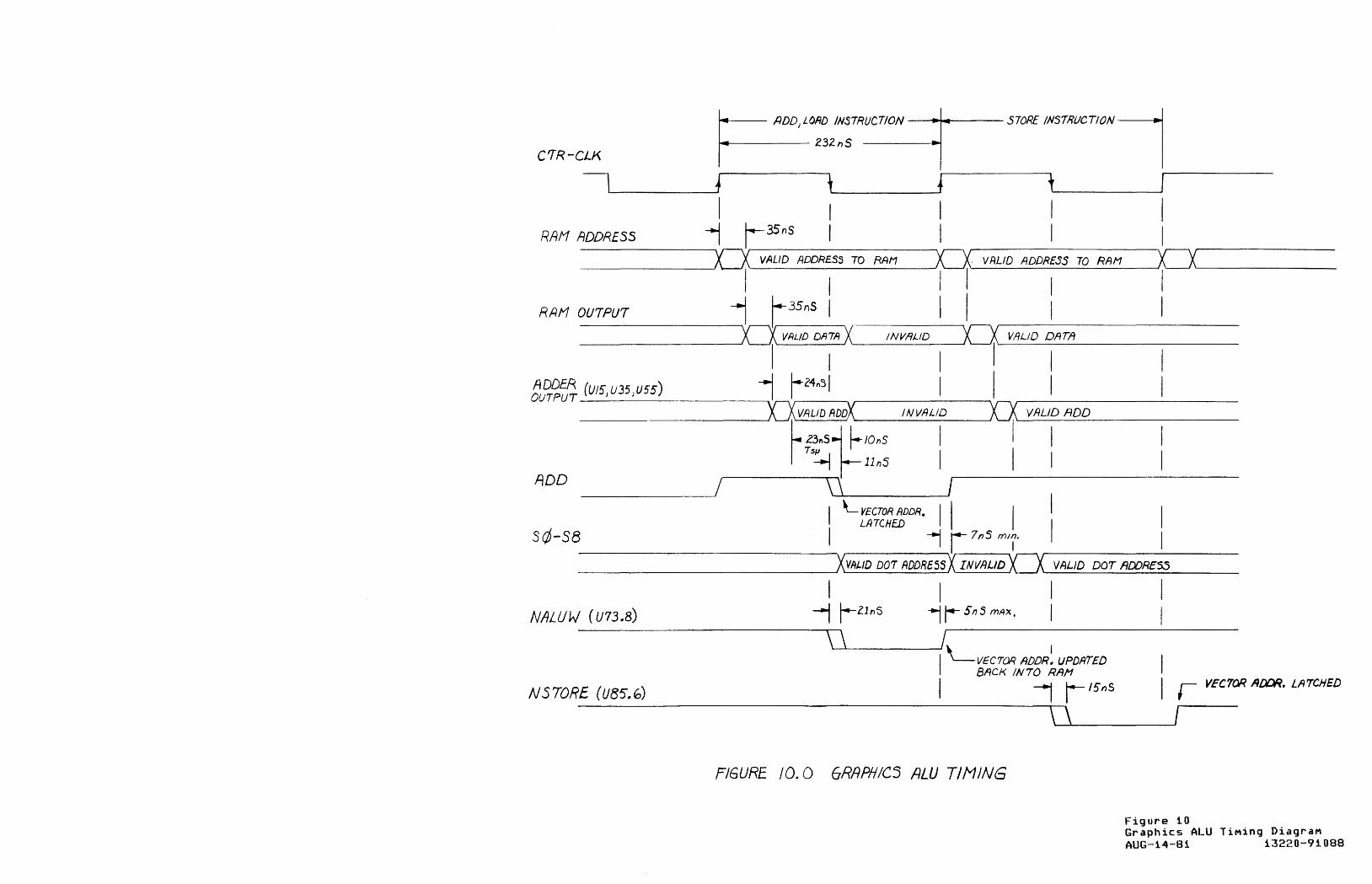
C'TR-CLK
~- ADD)LOI1D INSTRUCT/ON _ ..... j ....... ---S70RE IN57RUCTION1
14---- 232n5 1 1~ ____ ~1 l~ ____ ~t~----~tl ~ -----
I I I I I -1 r 35nS
r I I I -------~ ~LIDA~~roAAM ~-,-~-L-W-A-D-D-~-~-ro-R-AM--~-_____ _
I I I I II I I I I
-1 C35ns I I I I I --------0 VALID DATA '1~--/-N-VI1-/"'-ID--O VALID DATA
I I I
~J?!?!ti (U/5,U35,U55) 1 r2in31 I I _________ DVALIDADDX INVALID a VflLlD ADD
I I I I I I
I--- Z.3nS1 ~/OnS I I I I T~J-l1n5 I I I
____ Ir----~\ \ jr----------
I L VECTOR fWDR. II I I I LATCHED I I -, [7nS mIl' I
-------------XVALID D01 ADDRE5SX INVIlLID 0 VALID DOT flDDRESS
RAt1 ADDRESS
RAM OUTPUT
ADD
srj-S8
I I NALU W (U73 .8) -1 r-Z1nS "1 r- 5n5 mAX, I
--------....---,\ \ IL I
I VECTOR ADDR. UPDATED BACK IN70 RAM
NS70R£ (U85.~) I I i /5nS r VECTOR ADDR. Lft7CHED
\L--I,'---_-----J!
F/6URE 10.0 GRf1PHICS ALU TIMING
Figure 10 Graphics ALU TiMing DiagraM AUG-14-81 13220-91088

I D/SFLIlY FETCH-------t· .... I--·------ MEMORY READ ---.. ·I~·I---- DISPLAY FETCH MEI10RY WRITE I G eLK
I I I I I 11-'2n5
1 I I I 015 eye --~\~\--------------------~/~--------------------~\~\--------------------~I~--------------------~\~\-------
I I I I I I 1 r-rOnSI /-13fnS Ii I I I
---~\~.....l......-____ ----,I \l.---L\ _____ ----' \ - \ _m ___ J \'-----"-_____ ---' NGRFfS
I I I 10n51 ~I I I
G tvlU X ------------~\==~\----------~/~------==~----------~ I~----~\~~~----------~ _I 1- 17 nS 1 I I l, r1-DnS 1 I I
NGCfJ5 -----------------\~\ I~--------~~~~--------~ \ I~--------~~-_~\~ ________ ~ I I 1
1--/00,,5 -t -t I- 'C! "S mil). ~ r- 'OnS mm· I I I I I' I 'I
RAI1 DflT/I------------------------1( VALID }t------------------1( VAUD )}----------------------l( VALID )1-------------------------------I I I I
DLOD
6 VIDEO
M DOT
6 WRITE.
-1 /-/6n5 I I I ----------------------~D_J CLJ~-----------------------------
22/)S~~ 1 I 1 I I --II-to ~S min. I
________________________ ~nr_l~ __________________________________________ ~u_l~ ________________________________ _
i I
\ \ -I /-- lOllS MflX.
--------------------------------------------~~
-l I- ~DnS \, \
FIGURE 11.0 6RAPHICj VIDEO DI5PLA Y AND I1E/10RY WRI'TE 77t1IN6
Figure 11 Graphics Display and MeMory TiMing AUG-14-81 13220-91088

D07 RATE DRCX
GRAPHICS DOT ~YNCHRONIZATION
15.S~ ~ ! I I II I I I
NLC6AX (U98.13) ----.--n\:\ Ir---
I -I --I -I ----tt\
! 1j~S.~~ i I I I t~u89 II i
U97.14 -UN-K-NO-W-N-~X\J Ir---~\,___\",------"
U97.1l
U85.6
I : I I I : I I
_V_N_KN_O_WAJ __ U ..... --.--.\ \ /r------,\,.--,\
I: I I l+n51 H I I I
_____ ~" \\-_--Ij,..,,&b·l I I I I
I l I I I I
il
I
\ \ \ \ \"\ \ \
\ \ I \ , \ \ I \ , \
I J II I I \ I -1 1:1
UB?8 (DRCX.U89.&) ________________ fl~ _____ rl _______ rl~ ______ fl~ ____ ~fl~ ____ ~fl~ ______ fl~ ______ fl~ ____ _ I I I I
U98.1 C_U9_7t_U_+_DR_CX_) _____ ---+tlTl'--____ Ifl..L-____ ---"'rn ____ --"n'--___ n~ ______ n~ _____ n'___ _____ ~
6CLK UBB.6 (US7.8+ U98 .1) ____ --'
FIGURE 12.0 6RflPHICS DOT 5YNCRONIZA7/0N TIN/HB
Figure 12 Graphics Dot Clock Generation AUG-14-81 13220-91088

DOT RAT£. CLOCl<.
Z5. 7711Hz.
NLCGAX
SOF CLK
SOF
G eLI<.
17.18 11Hz.
START OF FRAH£ .... rr.------- s CH~R ------~,. ..... I·....------ -4 CHAR -------;~~I~~r----------3CHI}~-----------a ... '.c------- -z CHflR ---------'~
13nS 1 r CONTINI/ED @ BOT1l:t1
K\ I \1 ,-------------- ...
1111 3 nS WoRST CASE 5ET UP (SOF INPUT)
[ I I I
7 liS (HOI) 1 I \lJJr--T""""----\UJ~-r------ • •• CONTINUOUS
II 113 nS THRIJ SOF FLlP-Fl..OP
11/4 oS INACTIVE; CLEAR TO COUNT r FIRST GRIlPilIC {)()T OF WORD ¢
•••
GRAPHICS VIDEO
, ~4~-----------WOAD ¢ i I
i
OOT RI1TE CLOCK
6R11PHIC5 VIDEO
...... , * ___ ----~ -.1 CH~R-------,.-+, .... r-------lsr VIDEO CHARACTER ----.~,
I I
WORD 1
Jr--8,_r_IO-"X 81T 1/ X BIT 12. X 81T 13 X BIT 14 X BIT 15 X BIT ¢ X BIT 1 X BIT 2 X BIT 3 X 81T .,. X BIT S ~ .
'( BIT ¢ X BIT 1 X BIT Z X BIT 3 X BIT 4- X BIT 5 X Blr " X 81T 7 X 81T 8 Xr-B-IT- 9-C 7
CONTINUED
•••
FloURE. /3.0 5rART OF FRA/£ FOR GRAPHIC5 VIDEO TIMIN6
Figure 1".3 Start of FraMe TiMing DiagraM AUG-14-81 13220-91088

BLANK
NDeLK
Y ADDR
'-,1. Z CL.OCK ~ ,START OF COUNT IN ReTRflCE.
DeLAY I
2 S DtLAY it LZ8ns SET UP FOIl. 2 ewe/( DEI..Ii¥ LOAD I r-Z3ns SET UP FOR Y CLOCK (L511Z.) (INVERSE OF ReTRAce LOAD)
----~~~----------------------------------------------------------~~~ ~
Z5ns1 r ----------------------------------------------------------------------------~/~~/--------------------------------
Ifo.5nS 1 r tI I
-1 '8nS r PRE.VIO{JS ~DOReSS A~ff:;D x,--V,q-IJ.-ID-IIT-M-UX---------------
----------------------------------------------~~~~~-----~
FIGURE 14.0 6RAPHICS END OF LINE TIMING
Figure 14
1_
End of Line TiMing DiagraM AUG-14-81 13220-91088

DISTANCE BETWEEN TA~GET ~EGIST~AT ION HOLES 393.7±.016 MM
15.500±.D03 1
INCHES
02620-90088 10-22-81
SILKSCREEN
FIGURE 15.0 COMFOIJENT LI1'1~UT HEWLETT P"CKARD
rTlffiffiD LAYER 12
U ~~.!SN Fig u " e 1 S COMponent Layout Sheet AUG-14-81 13220-91088

z. NOTES:
51"3
Flgure 16 zao and Ports ScheMatic AUG-14-81 13220-91088
o \j ,... p v

VSY.NC. J
-::r: .... .1
/VI-Rex
«L (rJ.-:;---.¥b---1i6~O'l.H~2.'---______ .1..I3 fitJlliiiio
(Ql==:J:)-!M~RE~''''HIET[U!.)I'--______ l~'5 5>":5 CL(
(1
(.1
Zrxi-ZD7
7"NI'W
rBI/Sill<,
7N&US1I1C
J4-' ~~I Jt:lA
vs),,vc
~/J ~ j. ~ ~~----------------------------------~
SISI
I
Figuf'e 17 Vldeo and Display AUG-14-81
1 ) 6V1DELJ
J
1 )
1 )
MeMory ScheMatic L322()-·91 ()B8

A A i-
I TiX1
'I( Gilt J.S1..+f +sv~~y7 ~
(CZ~==:J~V~I'B~LUW~J~~--1----------------------1~-----------------llIfE ~4 TIU ~J.:510 • 2
JjU'1.3 Lf---------------r.I~~~~~~53;2
TNIfD ~" .;'--'
SJ2.
,AAA '4- i- ....
" " ~ j i
AA,A.,A. A +- ... .. ... ...
" t:-
~ ~ i ] ~ ~ i 1Il~ mfll1'
I~ ID3 ~
BII~Y
~~:t===~~~:~~~~~XL----------------------------------------------------------------------------------------------------------------------------t==r=T~~~M~~ln~t/~IJt.1~i!LIt;l I L l..:.h U~
'r /2 ... -NIl.,
rD7
!) "l6 1 SIS'}
~r---!:,.. Ii 1iI~
~: liZ" !IDIl3 '-..1: "3 D ii"p1:-
S3lO l'1 + " 5¢
$2$1
.~ .1 sl~ ~ 1..92S.,
1 U4-6
+5'1
NOTE:5:
1. IJJ.J.. R~71Wces IN OH/'IS , 20, AIJ.. RESIS1tJ/t.~ ODi4VATEl> ,-",Tit liN HS7EeAS<i("<*)
ME COI'fMON 1'!JJ.J.IJI's 1ll O/~ OI&YIe.ES. J. A/.J- ~flPlfCITO/cS IN "'''NID$ .
J
Figure 18 Vector Graphics ALU ScheMatic AUG-14-81 13220-91088

SC43
SCL2
I I
3 DOT 11011(
3 CUt.5TH6M
3 NRE3E'r1l
3 DOT R~ 'WRITE
N\oIM't
t5Y
UIJ5
$~ 3 DoTCI..A.
3 CTI..CJ..
81tH Pr<9tN¥JA14
=D. c" CIO, Cr.,C7, C5 1 C23,CU, C28, Cia
:B!
• TP3
1J:JrC: ,.,MIS -411CAS ~..-1D Vl'I'EIlS/tIWS t..fAS t "'.::AS" " "~S/tMt$. DII7It .rOE'S 1Z) ~ tfllHlS 111011 AIJM 1-7 *'U ~ ".(4 ~~ ~~.,. :/0 ifI..4,PltJ • +IZ.Y r= AM, PII-/ e -~V ~ IW.) PlIJ .1
COiI_ TO 1iIJ;., P/~ 'il
+5V
+!iV
I IIII f~ +5V
3
.~----------------------------------~~~~+~
Figure 19 Vector Graphics Display ScheMatic AUG-14-S1 13220-910S8
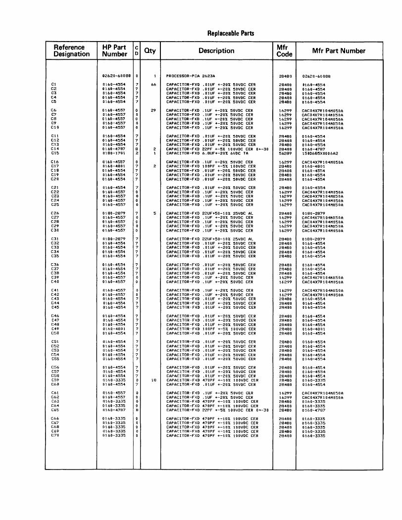
Replaceable Parts
Reference HP Part c Qty Description Mfr Mfr Part Number Designation Number 0 Code
02620-60088 0 1 PROCESSOR-peA 2623A 28480 02620 -60 088
C1 0:160-4554 7 66 CAPACITOR-FXD .01UF +-20% 50VDC CER 28480 0160-4554 C2 0160-4554 7 CAPACITOR-FXD .01UF +-20% 50VDC CER 28480 0160-4554 C3 0"160-4554 7 CAPACITOR-FXD .01lIF +-20% 50VDC CER 28480 0160-4554 C4 0160-4554 7 CAPACITOR-FXD .01UF +-20'% 50VDC CER 28480 0160-4554 C5 0~160-4554 7 CAPACITOR-FXD .01UF +-20'% 50VDC CER 28480 0160-4554
Co 0160-4557 0 29 CAPACITOR-FXD .1UF +-20% 50VDC CER 16299 CAC04X7Rl04M050A C7 0~160-4557 0 CAPACITOR-FXD .1UF +-20% 50VDC CER 16299 CAC04X7R104M050A C8 0160-4557 0 CAPACITOR-FXD .1UF +-20% 50VDC CER 16299 CAC04X7Rl04M050A C9 0160-4557 0 CAPACITOR-FXD .1UF +-20% 50VDC CER 16299 CAC04X7Rl04M050A C10 o "ll60-4557 0 CAPACITOR-FXD .1UF +-20% 50VDC CER 16299 CAC04X7Rl04M050A
Cl1 01160-4554 7 CAPACITOR-FXD .OlUF +-20% 50VDC CER 28480 0160-4554 C12 0"1160-4554 7 CAPACITOR-FXD .01UF +-20% 50VDC CER 28480 0160-4554 C13 0160-4554 7 CAPACITDR-FXD .01UF +-20% 50VDC CER 28480 0160-4554 C14 0160-4787 8 2 CAPACITOR-FXD 22PF +-5% 100VDC CER 0+-30 28480 0160-4787 C15 0180-1701 2 1 CAPACITOR-FXD 6.8UF+-20% 6VDC TA 56289 150D685XOO06A2
C16 0"160-4557 0 CAPACITOR-FXD .1UF +-20% 50VDC CER 16299 CAC04X7Rl04M050A C17 0160-4801 7 2 CAPACITOR-FXD 100PF +-5% 100VDC CER 28480 0160-4801 C18 01. 60-4554 7 CAPACITOR-FXD .01UF +-20% 50VDC CER 28480 0160-4554 C19 0160-4554 7 CAPACITDR-FXD .01UF +-20% 50VDC CER 28480 0160-4554 C20 01.60-4554 7 CAPACITOR-FXD .01UF +-20% 50VDC CER 28480 0160-4554
C21 0160-4554 7 CAPACITOR-FXD .01UF +-20% 50VDC CER 28480 0160-4554 C22 0160-4557 0 CAPACITOR-FXD .1UF +-20% 50VDC CER 16299 CAC04X7Rl04M050A C23 0160-4557 0 CAPACITOR-FXD .1UF +-20% 50VDC CER 16299 CAC04X7R104M050A C24 0"1160-4557 0 CAPACITOR-FXD .1UF +-20% 50VDC CER 16299 CAC04X7R104M050A C25 01160-4557 0 CAPACITOR-"FXD .1UF +-20% 50VDC CER 16299 CAC04X7R104M050A
C26 0'1. 80-2879 7 5 CAPACITOR-FXD 22UF+50-10% 25VDC At 28480 0180-2879 C27 01160-4557 0 CAPACITDR-·FXD .1UF ~"-20% 50VDC CER 16299 CAC04X7R104M050A C28 01. 60-4557 0 CAPACITOR-FXD .1UF +-20% 50VDC CER 16299 CAC04X7Rl04M050A C29 01160-45~j7 0 CAPACITDR-FXD .1UF +-20% 50VDC CER 16299 CAC04X7R104M050A C30 01.60-4557 0 CAPACITOR-FXD .1UF +-20% 50VDC CER 16299 CAC04X7Rl04M050A
C31 01:80-2879 7 CAPACITOR-FXD 22lJF+50-10% 25VDC AL 28480 0180-2879 C32 01.60-4554 7 CAPACITOR-FI<D .01UF +-20% 50VDC CER 28480 0160-4554 C33 01.60-4554 7 CAPACITOR-FXD .0tuF +-2OX 50VDC CER 28480 0160-4554 C34 01. 60-4554 7 CAPACITOR-FI<D .01UF +-20% 50VDC CER 28480 0160-4554 C35 01.60-4554 7 CAPACITDR-"FXD .01LJF +-20% 50VDC CER 28480 0160-4554
C~36 0160-4554 7 CAPACITOR-FXD .01UF +-20% 50VDC CER 28480 o 160-45~j4 C37 01.60-4554 7 CAPACITDR-"FXD .01UF +-20% 50VDC CER 28480 0160-4554 C~58 01. 60-4554 7 CAPACITOR-FXD .01UF +-20% 50VDC CER 28480 0160-4554 C39 01.60-45~j7 0 CAPACITOR-F)(D . tuF +-20::C: 50VDC CER 16299 CAC04X7Rl04M050A C40 0160-4557 0 CAPACITOR-FXD .1UF +-20% 50VDC CER 1~,299 CAC04X7Rl04M050A
C41 o 1. 60-45~17 0 CAPACITOR-FXD .1UF +-20::C: 50VDC CER 16299 CAC04X7Rl04M050A C42 O"J. 60-4557 0 CAPACITOR-nD .1UF +-20% 50VDC CER 16299 CAC04X7R104M050A C43 01:60-4554 7 CAPACITOR-"'FXD .01lJF +-'20% 50VDC CER 28480 0160-4554 C44 01.60-4554 7 CAPACITOR-FXD .01UF +-20% 50VDC CER 28480 0160-4554 C45 01160-4554 7 CAPACITDR-·FXD .01LJF +-20% 50VDC CER 28480 0160-4554
C46 01. 60-4554 7 CAPACITOR-FXD .01UF +-20% 50VDC CER 28480 0160-4554 C47 01:60-4554 7 CAPACITOR-"·F)(D .01UF +-20% 50VDC CER 28480 0160-4554 C48 0160-4554 7 CAPAC ITOR -FXD .01UF +-20% 50VDC CER 28480 0160-4554 C49 01.60-4801 "l CAPACITDR···F)(D 100PF +-5% 100VDC CER 28480 0160-4801 C~jO 0"160-4554 7 CAPACITOR'-F)(D .01UF +-20% 50VDC CER 28480 0160-4554
C51 01.60-45~i4 7 CAPACITDR-'"F)(D .01UF +-20% 50VDC CER 28480 0160-4554 C~52 01.60-45:14 7 CAPACITOR-FXD .01UF +-20% 50VDC CER 28480 0160-4554 [:53 01.60-4554 7 CAPACITDR-F)(D .0 lllF +-20% 50VDC CER 28480 o 160-45:'.'i4 C~j4 () 160-4554 7 CAPACITOR-nD .01UF +-2()% 50VDC CER 28480 0160-4554 (;55 o 1. 60-45~i4 7 CAPACITDR--nD ,OllJF +-20'% 50VDC CER 28480 0160-4554
C~:j6 0160-45~i4 7 CAPACITOR-nD .01UF +-20% 50VDC CER 28480 0160-4554 C57 01.60-4554 7 CAPACITDR-·F)(D . 0 lllF +-20'% 50VDC CER 28480 0160-4:'.';54 C~j8 0160-4554 7 CAPACITOR-nD .01UF +-20% 50VDC CER 28480 0160-4554 [:59 0160-3335 0 lEl CAPACITOR-FI(D 470PF +-10'% 100VDC CER 28480 0160-3335 C60 O"J 60-45~i4 7 CAPACITOR-nD .01UF +-20% 50VDC CER 28480 0160-4554
C61 0160-45~;7 0 CAPACITOR-FI(D .1UF +-20% 50VDC CER 16299 CAC04X7Rl04M050A C62 0'160-4557 0 CAPACITOR-F:(D .1UF +-20% 50VDC CER 16299 CAC04X7Rl04M050A [:63 0160-3335 0 CAPACITOR·_·FXD 470PF +-1 OX 100VDC CER 28480 0160-3335 Ctl4 0160-3335 0 CAPACITOR-F:(D 470PF +-10% 100VDC CER 28480 0160-3335 C65 0160-47El7 B CAPACITOR-FXD 22PF +-5% 100VDC CER 0+-30 28480 0160-4787
C66 0160-3335 0 CAPACITOR-FXD 470PF +-10% 100VDC CER 213480 0160-3335 C67 0160-3335 0 CAPACITOR--F:(D 470PF +-10% 100VDC CER 28480 0160-3335 C68 0160-3335 0 CAP AC I TOR -F:(D 470PF +-10% 100VDC CER 28480 0160-3335 C69 0160-3335 0 CAPACITDR-"F:(D 470PF +-10% 100VDC CER 28480 0160-3335 C'70 0160-3335 0 CAPACITOR-FXD 470PF +-10% 100VDC CER 28480 0160-3335

Replaceable Parts
Reference HP Part c aty Description Mfr Mfr Part Number Designation Number 0 Code
C71 0160-3335 0 CAPACITOR-·FXD 470PF +-10X 100VDC CER 28480 0160-3335 C72 0160-3335 0 CAPACITOR-FXD 470PF +-10'% 100VDC CER 28480 0160-3335 cn 0160-3335 0 CAPACITOR·_·FXD 470PF i'-lOX 100VDC CER 28480 0160-3335 C74 0160-4554 7 CAPACITOR-FXD ,01UF +-20X 50VDC CER 213480 0160-4554 C75 0160-4554 7 CAPACITOR-FXD ,01lJF +-20'% 50VDC CER 213480 0160-4554
C76 0160-4554 7 CAPACITOR-FXD ,01UF +-20X 50VDC CER 213480 0160-4554 cn 0160-4554 7 CAPACITOR-FXD ,01l.JF +-20'% 50Vl)C CER 28480 0160-4554 C78 0160-4554 7 CAPACITOR-FXD ,01UF +-20'% 50VDC CER 28480 0160-4554 C79 0160-4554 7 CAPACITOR-FXD ,01LJF +-20'% 50VDC CER ;:>13480 0160-4554 CBO 0160-4554 7 CAPACITOR-FXD ,01UF +-20'% 50VDC CER 28480 0160-4554
C81 0160-4554 7 CAPACITOR-·FXD ,01UF +-20'% 50VDC CER 28480 0160-4554 C82 0160-4554 7 CAPACITOR-FXD ,01UF +-·20X 50VDC CER 2f:1480 0160-4554 C83 0160-4557 0 CAPACITOR-·FXD ,1UF +-·20% 50VDC CER 16299 CAC04X7Rl04H050A C84 0160-4557 0 CAPACITOR-FXD ,111F +-20'% 50VDC CER 16299 CAC04X7Rl04M050A C85 0160-3335 0 CAPACITOR-·FXD 470PF +-lOX 100VDC CER 21:1480 0160-3335
CBb 01 bO-3335 0 CAPACITOR-FXD 470PF +·-10X 100VDC CER 2f:148 0 0160-3335 C87 0160-3335 0 CAPACITOR-·FXD 470PF +-10X 100VDC CER 28480 o 1 ~,0-3335 CB8 0160-3335 0 CAPACITOR-FXD 470PF +·-10X 100VDC CER 2f:l480 0160-3335 C89 0160-4554 7 CAPACITOR-·FXD ,01UF +-20X 50VDC CER 28480 0160-4554 C90 0160-4554 7 CAPAC ITOR -FXD ,01UF +-20:;(; 50VDC CER 2f:1480 0160',-4554
C91 0160-4554 7 CAPACITOR-FXD ,01UF +-20X 50VDC CER 28480 0160-4~i54
cn 0160-4554 7 CAPACITOR -FXD ,01UF +-20% 50VDC CER 213480 0160-4554 C93 0160-4554 7 CAPACITDR-·FXD .0tI.JF +-20X 50VDC CER 2f:l4BO 0160-4554 C94 0160-4554 7 CAPACITOR-FXD ,01UF +-20X 50VDC CER 28480 0160-4554 C9'5 0160-4554 7 CAPACITOR-··FXD ,01UF +-20X 50VDC CER 21:1480 0160-4554
C96 0160-4554 7 CAPACITOR-FXD ,01UF +-·20% 50VDC CER 28480 0160'-4554 C97 0160-4554 7 CAPACITOR-·FXD ,01UF +-20'% 50VDC CER ::.'13480 0160-4554 C98 0160-4557 0 CAPACITOR-FXD ,1UF +-20% 50VDC CER 16299 CAC04X7Rl04M050A C99 0160-4557 0 CAPACITOR-·FXD .1UF +-20X 50VDC CER 16;?99 CAC04X7Rl04H050A ClOD 0160-4557 0 CAPACITOR-FXD ,1UF +-20% 51lVDC CER 16;~99 CACIl4X7R104M050A
ClOt 0160-4557 0 CAPACITOR-·FXD , tlJF +-·20X 50VDC CER 16299 CAC04X7Rl04H050A Cl02 0160-4554 7 CAPACITOR-FXD ,01UF +-20% 50VDC CER 2B480 0160-4554 Cl03 0160-4554 7 CAPACITOR·_·FXD ,01lJF +-20% 50VDC CER 28480 0160-4554 Cl04 0160-4554 7 CAPACITOR-FXD ,01UF +-20% 50VDC C:ER 2f.l480 0160-4554 Cl05 0160-4554 7 CAPACITDR-·FXD ,01lJF +-20'% 50VDC CER 213480 0160-4554
Cl06 0160-45504 7 CAPACITOR-FXD ,01UF +-20X 50VDC CER 2£:1480 0160'-4554 Cl07 0160-4554 7 CAPACITDR····FXD .0lUF +-20% 50VDC CER 28480 0160-4554 Cl08 0160-4554 7 CAPACITOR-FXD ,01UF +-20% 50VDC CER 2B480 0160-4554 Cl09 0160-4554 7 CAPACITOR-FXD ,01LJF +-20% 50VDC CER 28480 0160-4554 Cl10 0160-4557 0 CAPACITOR-FXD ,1L1F +-20% 50VDC CER 16299 CAC04X7RI04M050A
C111 0160-4557 0 CAPACITDR-FXD ,1UF +-20% SOVDC CER 11.299 CAC04X7Rl04M050A C112 0160-3335 0 CAPACITOR-FXD 470PF +,-10% 100VDC CER 21:1480 0160-3335 Cl13 0160-3335 0 CAPACITDR--FXD 470PF +-10% 100VDC CE.R 213480 0160-3335 C114 0160-4554 7 CAPACITOR-FXD ,01L1F +-20X 50VDC CER 213480 0160-4554 Cl15 0160-4557 0 CAPACITOR-·FXD ,1UF +-20% 50VDC CER 16299 CAC04X7Rl04H050A
C1l6 0160-3335 0 CAPACITOR-FXD 470PF +-10% 100VDC CER 21)480 0160-3335 Cl17 0160-4554 7 CAPACITOR-·FXD ,OlLJF +,-20% 50VDC CER 213480 0160-4554 C1l8 0180-2879 7 CAPACITOR-FXD 22UF+50-10% 25VDC AL 2f:l48 0 0180-2879 C119 0180-2879 7 CAPACITOR--FXD 22UF+50-"10% 2~iVDC AL •. '13480 01130-2879 C120 0180-2879 7 CAPACITOR-FXD 22L1F+50-10% 25VDC AL 2B4f.l0 0180-2879
C121 0160-4554 7 CAPACITDR-·FXD ,01UF +·_·20% 50VDC CER :'.0480 0160-4554 C122 0160-4554 7 CAPACITOR-FXD ,01UF +-20% 50VDC CER 2f.l480 OH.0-4554 C12J 0160-4554 7 CAPAClTOR-··FXD .01UF +-,,20% 50VDC CER ;:'.13480 0160-4554
CRl 1901-0050 3 9 DIOl)E-SWITCHING 80V 200M 2NS DO-3~i 2B4f.lO 1901-0050 CR2 1901-0050 3 DIODE-SWITCHING BOV 200MA 2NS DO-35 2f:l48 0 1 '701-0050 CR3 1';>01-0050 3 DIODE-SWITCHING 80V 200MA 2NS DO-35 2B4BO 1<101-0050 CR4 1901-0050 3 DIODE-SWITCHING 80V 200MA 2NS DO-35 ;",8480 1 '701-0050 CR5 1901-0050 3 DIODE-SWITCHING 80V 200MA 2NS DO-35 20480 1901,-0050
CR6 1901-0050 3 DIODE-SWITCHING 80V 200MA ;~NS DO-35 28480 1 '701-0050 CR7 1901-0050 3 DIODE-SWITCHING 80V 200M 2NS DO-35 20480 1901--0050 CR8 1902-0952 6 1 DIODE··-ZNR 5,6V 5% DO-35 PD=,4W TC=+,046% 2f:l4BO 1902-0952 CR9 1902-0976 4 5 DIODE-ZNR 14,5V PD=5W TC=+,088X IR=5UA 1"1 </61 1 ,~;SE18C CR10 1902-0976 4 DIODE·-ZNR 14,5V PD=5W TC=+,08B% IR=5UA 11961 1.5SElI3C
CRtt 1902-0976 4 DIODE-ZNR 14,5V PD=5W TC=+,088X IR=5I.1A 11961 1.5HF.:18C CR12 1902-0976 4 DIODE-ZNR 14,5V PD=5W TC=+,088% IR=::'iUA 11961 1. 5SEl BC CR13 1902-0976 4 DIODE-ZNR 14,5V PD=5W TC=+,088X IR=5UA 11961 1,5HE18C CR1.o4 1901-0050 3 DIODE-SWITCHING 80V 200MA 2NS DO-35 ?B480 1 ';>01-0050 CR15 1901-0050 3 DIODE-SWITCHING 80V 200MA 2NS DO-35 2B480 1901,-0050
CRlb 1902-0041 4 1 DIODE--ZNR 5,11V 5% DO-35 P1>=,4W i'.B48 0 1902-0041
Jl 1251-5500 9 2 CONNECTOR 26-PIN M POST TYPE 28480 1~~51-5500
J2 1251-5521 4 1 CONNECTOR 9-·PIN 11 POST TYPE 2El480 1251-5521 J3 1251-5520 3 1 CONNECTOR 7-PIN 11 POST TYPE 2B480 1251-5520 J4 1251-5499 5 1 CONNECTOR 16····PIN 11 POST TYPE 28480 1;:?51-5499 J5 1251-5500 9 CONNECTOR 26-PIN M POST TYPE 28480 12:";1-5500

Replaceable Parts
Reference HP Part c Qty Description Mfr Mfr Part Number Designation Number 0 Code
J6 12:':il-5546 3 1 CONNECTOR 34'-PIN H POST TYPE 28480 1251-5546
Ql 1 B~,3-0281 9 1 TRANSISTOR PHP 2N2907A SI TO-18 PD=4001'lW 04713 2N2907A Q2 18::i4-0467 5 2 TRANSISTOR NPN 2N440l SI TO-92 PD=310MW 03508 2N4401 Q3 18~;4-0 019 3 1 TRANSISTOR NI'N SI TO-18 PD=360MW 28480 1854-0019 Q4 18~i3-0036 2 1 TRANSISTOR PNP SI PD=310MW FT=250MHZ 28480 1853-0036 (;15 lfj~;4-0467 5 TRANSISTOR NPN 2N4401 SI TO·-92 PD=310MW 03508 2N4401
Rl 1810-0275 1 3 NETWORK-RES 'l0-SIP1.01< OHM X 9 01121 210Al02 R2 0663-102:5 9 28 RESISTOR 11< !5X .25W FC TC=-400/+600 01121 CB1025 R3 06B3-1025 9 RESISTOR 11< !5X .25W FC TC=-400/+600 01121 CB1025 R4 0663-102:5 9 RESISTOR 11< 5X .25W FC TC=-400/+600 01121 CB1025 R5 06B3-103:5i 1 4 RESISTOR 101< 5X .25W FC TC=-400/+700 01121 CB10:55
R6 0683-1025 9 RESISTOR lK !5X .25W FC TC=-400/+600 01121 CB1025 R7 0683-4715 0 6 RESISTOR 470 5X .2SW FC TC=-400/+600 01121 CB4715 R8 0683-470:5 8 15 RESISTOR 47 :5X .25W FC TC=-400/+500 01121 CB4705 R9 06B3-151:5, 2 3 RESISTOR 150 SX .2SW FC TC=-400/+600 01121 CB1515 Rl0 0683-102:5 9 RESISTOR lK :iX .25W FC TC=-400/+600 01121 CB1025
Rl1 0683-471:5, 0 RESISTOR 470 5X .25W FC TC=-400/+600 01121 CB4715 R12 06B3-101:5 7 2 RESISTOR 100 5X .25W FC TC=-400/+500 01121 CB101S R13 06133-1025 9 RESISTOR 11< :'iX .25W FC TC=-400/+600 01121 CB1025 R14 0683-4715 0 RESISTOR 470 5X .25W FC TC=-400/+600 01121 CB4715 R15 0683-102:5 9 RESISTOR 11< :'iX .25W FC TC=-400/+600 01121 CB1025
R16 0683-220:5 9 8 RESISTOR 22 :iX .25W FC TC=-400/+500 01121 CB2205 R17 0683-220:5 9 RESISTOR 22 :iX .25W FC TC=-'400/+500 01121 CB2~~05 R1B 0683-220:5 9 RESISTOR 22 :iX .25W FC TC=-400/+500 01121 CB2205 R19 0683-220:5 9 RESISTOR 22 :iX .25W FC TC=-400/+500 01121 CB2;~05 R20 068:3-2205 9 RESISTOR 22 ~)% .25W FC TC=-400/+500 01121 CB2205
R21 0683-2205 9 RESISTOR 22 :iX .2SW FC TC=-AOO/+500 01121 CB2205 R~!2 0683-220:5 9 RESISTOR 22 :iX .25W FC TC=-400/+500 01121 CB2205 R25 0683-1025 9 RESISTOR 11< ~)% .2SW FC TC=-400/+600 01121 CB1025 R26 068:3-1025 9 RESISTOR lK :iX .25W FC TC=-400/+600 01121 CB1025 R27 068:3-1025 9 RESISTOR lK :'iX .25W FC TC=-400/+600 01121 CB1025
R28 0683-1025 9 RESISTOR lK :;X .2SW FC TC=-400/+600 01121 CB102S R29 0683-1515 2 RESISTOR lS0 S% .2SW FC TC=-400/+600 01121 CB151S R30 0683-1025 9 RESISTOR lK ~;X .25W FC TC=-400/+600 01121 CB1025 R31 1810-0275 1 NETWORK-·RES 1. O""SIP 1 . 01< OHM X 9 01121 21 OAl 02 R32 0683-4705 8 RESISTOR 47 ~jX .2SW FC TC=-400/+S00 01121 CB4705
R33 0683-4705 8 RESISTOR 47 ~iX .25W FC TC=-400/+500 01121 CB4705 R~'34 0683-470S 8 RESISTOR 47 ~jX .2SW FC TC=-400/+500 01121 CB4705 R35 0683-4705 8 RESISTOR 47 ~i% .25101 FC TC=-400/+S00 01121 CB4705 R36 0683-151:5 2 RESISTOR lS0 5'X. .25W FC TC=-400/+600 01121 CB1S15 R37 0683-1015 7 RESISTOR 100 5X .25W FC TC=-400/+500 01121 CBl 015
R:'38 0683-2205 9 RESISTOR 22 ~jX .25W Fe TC=-400/+500 01121 CB2205 R39 0683-4715 0 RESISTOR 470 5X .25W FC TC=-400/+600 01121 CB4715 R40 0683-1025 9 RESISTOR lK ~i'X. .25101 FC TC=-400/+600 01121 CB1025 R41 0683-1025 9 RESISTOR II< ~j'X. .2SW FC TC=-400/+600 01121 CB1 O;~5 R42 0683-1025 9 RESISTOR lK :j% .2SW FC TC=-400/+600 01121 CB1025
R44 0683-1035 1 RESISTOR 10K 5X .25W FC TC=-400/+700 01121 CB1035 R~:;l 0683-1025 9 RESISTOR lK ~;7. .25W FC TC=-400/+600 01 1~~1 CB102S R52 0683-1025 9 RESISTOR II< ~iX .2SW FC TC=-400/+600 01121 CB1025 R:7j3 0683-1025 9 RESISTOR lK ~iX .25W FC TC=-400/+600 01121 CB1025 R54 0683-1025 9 RESISTOR 11< ~;X .25W FC TC=-400/+600 01121 CBl025
R55 0683-4735 4 1 RESISTOR 47K 5X .25101 FC TC=-400/+BOO 01121 CB4735 R5!> 0683-1025 9 RESISTOR lK ~i% .25W FC TC=-400/+600 01121 CB1025 R~57 0683-1025 9 RESISTOR lK ~;7. .25W FC TC=-400/+600 01121 CB1025 R58 0683-4725 2 1 RESISTOR 4.n 5% .25W FC TC=-400/+700 01121 CB47;~5 R~j9 0683-1025 9 RESISTOR lK ~j" .25W FC TC=-400/+600 01121 CBI025
R61 0683-5615 1 1 RESISTOR S60 ~i% .25101 FC TC=-400/+600 01121 CB5615 R62 0686-2215 7 1 RESISTOR 220 5% .5W CC T[;=0+529 01121 EB2?15 r~63 0683-1025 9 RESISTOR 11< !:jX .25101 FC TC=-400/+600 01121 CB1025 R64 0683-4'715 0 RESISTOR 470 5% .2SW FC TC=-400/+600 01121 CB4715 R6'5 0683-4715 0 RESISTOR 470 ~i'X. .25101 FC TC=-400/+600 01121 CB4715
R6!> 0683-1025 9 RESISTOR lK ~j" .2SW FC TC=-400/+600 01121 CBI025 R68 06133-1025 9 RESISTOR lK ~j" .2SW FC TC=-400/+600 01121 CB1025 R69 0683-1025 9 RESISTOR lK ~iX ,25W Fe TC=-400/+600 01121 CB1025 R70 0683-1025 9 RESISTOR 11< ~i% .25W Fe TC=-400/+600 01121 CBl 0;':~5 R'7l 0683-1035 1 RESISTOR 10K 5% .25W FC TC=-400/+700 01121 CBI035
R72 1810-0275 1 NETWORK-·RES 1 0-·SIP1. OK OHI1 X 9 01121 21 OAl 02 R'73 0683-4'705 8 RESISTOR 47 ~i'X. .2SW FC TC=-400/+500 01121 CB4705 R74 0683-4705 B RESISTOR 47 ~i" .25W Fe TC=-400/+500 01121 CB4705 R7'5 0683-4'705 8 RESISTOR 47 ~,'X. ,25101 Fe TC=-400/+500 01121 CB4705 R76 0683-4705 8 RESISTOR 47 ::',X .2SW FC TC=-400/+500 01121 CB4705
R77 0683-4705 8 RESISTOR 47 ~jX .25W Fe TC=-400/+500 01121 CB4705 R78 0683-4705 8 RESISTOR 47 !':iX ,2SW FC TC=-400/+500 01121 CB4705 R'79 0683-4'705 8 RESISTOR 47 ~'X. ,25101 Fe TC=-400/+500 01121 CB470S R80 0683-4705 8 RESISTOR 47 ::"% ,25W Fe TC=-400/+S00 01121 CB4705 R8t 0683-4705 8 RESISTOR 47 ::,X ,,25W Fe TC=-400/+500 01121 CB4705

Replaceable Parts
Reference HP Part c Qty Description Mfr Mfr Part Number Designation Number D Code
R82 0683-4705 8 RESI!HOR 47 5% ,25W FC TC=-'400/+500 () 1121 CB4705 REl3 0683-1035 1 RESISTOR 10K 5% ,25W Fe TC=-400/+700 01121 CFl10:55 R84 0683-1025 9 RESISTOR lK ~;% ,25W FC TC=--400/+600 01121 CBl O;~5
TPl-TP19 0360-0124 3 19 CONNECTOR-SGL CONT PIN ,04····IN-BSC-SZ RND 28480 0360·-·0124
U14 1820-1441 6 3 IC ADl>R TTL LS BIN FULL ADl>R 4"-BIT Ot;.:'95 SN74LS283N U15 1820-1445 0 3 IC LCH TTL LS 4--(1 IT 0129::' SN74LS375N U16 1820-1438 1 7 IC MUXR/DATA-SEL TTL LS ?"-'TO-1'-LINE QUAD 01 ;':~95 SN74LS257AN U17 1820-1432 ::; 6 IC CNTR TTL LS BIN SYNCHRO POS-EDGE-TlHG 01295 SN74LS163AN U18 1820-1997 7 3 IC FF TTL l.S D'-TYPE POS-··EDGE-·TR IG PRl.-·IN 01 ;:!95 SN74l..S374N
U19 1820-1457 4 2 Ie SHF-RGTR TTL S D'-TYPE PRL-IN PRL-OlJT 01295 SN74S299N U21 1816-0724 7 6 IC TTL S 64····BIT STAT RAM :35-·NS 3-8 01295 SN74S189N U22 1816-1472 4 1 IC TTL S 256-(lIT ROM 50-NB 3-S 34~~71 HM3'-7603-5 PROGRAMMED U23 1820-1858 9 5 IC FF TTL L.S D-TYPE OC1L 01295 SN74LS~~77N Ll24 11:116-0724 7 Ie TTL S 64-BIT STAT RAM 35·-NS 3-S 01295 SN74S189N
1J25 1820-1858 9 IC FF TTL LS D-·TYPE DCTL ()1295 SN74LS377N U26 tE120-1438 1 IC MlJXRlDATA·-SEL TTL LS 2·-·TO-l-l..INE QUAD 01295 SN74LS257AN U28 1820-1112 8 7 Ie FF TTL LS D····TYPE POS-"EDGE-l RIG 01295 SN74l..S74AN U28 1820-1997 7 Ie FF TTL LS D··-TYPE POS--EDGE-TR IG PRL-IN 01295 SN'74l..S374N U29 1820-1457 4 IC SHF-RGTR TTL. S D·-TYPE PRL-IN PRL-·OUT 01295 SN74S299N
lJ31 11:120-1432 5 Ie CNTR TTL. LS BIN SYNCHI~() POS-EDGE-TRIG 01295 SN74LS163AN U32 18~~0-1432 5 Ie CNTR TTL. l..S BIN SYNCHRO POS-EDGF.:-·TRIG 01295 SN74LS163AN U33 1£:116-0724 7 Ie TTL S 64-BIT STAT RAM 35·-NS 3-S 01295 SN74S189N U34 1820-1441 6 Ie ADDR TTL. L.S BIN FUl.L ADDR 4-BIT 01295 SN74LS283N U35 H120-:1445 0 Ie LCH TTL LS 4--(lJT 01295 SN741 .. S375N
U36 1820-1438 1 IC MUXR IDATA-·SEL TTL L.S ?,·-TO·-1····LINE r~UAD 01;:~95 SN7·4LS257AN U37 1820-1430 3 3 Ie CNTR TTl.. l..S BIN SYNCHRl1 POS'-EDGE-TRIG 01295 SN74LS161AN U38 1820-2024 3 7 IC l>RVR TTL LS LINE DRVR OCTL 01295 SN74LS244N Ll39 1820-1298 1 1 Ie MUXR/DATA·-SEL TTL LS 8"-TCI-l-LINE 01295 SN74LS251N U41 1820-1240 3 2 Ie DCDR TTL S 3·-TO-8-··LINE 3-INP 01295 SN74S13BN
U42 1816-1471 3 1 IC TTL S 2S6-BIT ROM 50-NS 3-'S 34371 HM~~""7603-5 PROGRAMMED U43 1820-1858 9 Ie FF TTL LS D-··TYPE OCTL 012';>5 SN74LS377N U44 1816-0724 7 Ie TTL S 64-BIT STAT RAM 35·-NS 3"-S 01295 SN74S189N U45 1820-1858 9 IC FF TTL LS D'-'TYPE OCTl.. 01 (!95 SN74LS377N U46 1f.120-1438 1 Ie MUXR/DATA-SEL TTL L.S 2--TO'-1-LINE QlIAD 01 ;:'95 SN74L.S257AN
U47 1820-1430 3 IC CNTR TTL LS BIN SYNCHRO P OS'-'EDGE -'1 RIG 01 ;~95 SN74LS161AN U48 1820-1987 5 2 IC SHF-RGTR TTL LS COM CLEAR STOR 8····BIT 01295 SN74LS299N U49 1820-1858 9 Ie FF TTL LS D-'TYPE OCTL 01295 SN74LS377N U51 1f.120-1112 8 Ie FF TTL LS D'-TYPE POS-EDGE-TRIG 01295 SN'74LS74AN 1J52 1820-1438 1 IC MLJXR IDATA-SEl. TTL L.S 2-TO·-1····LINE QUAD 01~~'t~; SN74LS257AN
U53 11:116-0724 7 IC TTL S 64-BIT STAT RAM 35·-NB 3-S 01295 SN74B189N U54 1820-1441 6 Ie ADl>R TTL L.S BIN FULL ADDR 4-BIT o 1 ~~95 SN74LS283N U55 1f.120-1445 0 IC LCH TTL LS 4-··BIT 0129~:; BN74L.S375N U57 1820-1432 5 IC CNTR TTL LS BIN SYNCHRO POS-'(DGE-TR IG o 1 ;:~95 BN74I..S16:SAN US8 1820-1322 2 3 Ie GATE TTL S NOR QUAD 2-··INP 01295 SN74S02N
1J59 1820-1432 5 IC CNTR TTL. LS BIN SYNCHRO P OS""EDGE ... TR I G 01295 SN74LS163AN U61 11:120-1112 8 IC FF TTL LB D··-TYPE POS-EDGE-TRIG 01295 SN74LS74AN U62 1820-1244 7 1 Ie MUXR/DATA-SEL TTL l..S ·4--TO-l-·LINE DUAL 01295 SN74LS153N U63 1B20-1112 8 Ie FF TTL LS D'-TYPE POS-'EDGE-TR IG 01295 SN74LS74AN Ub4 1816-0724 7 IC TTL S 64-'BIT STAT RAM 35-·NS 3-S 01295 SN74S189N
U65 1820-1112 8 Ie FF TTL LS D··-TYPE POS-EDGE-TRIG 01295 SN74LS74AN \J66 1820-1212 9 1 Ie FF TTL LS J"K NEG··EDGE·-TRIG 01295 SN74LS112AN U66 1820-1303 9 5 IC SHF-RGTR TTL S R-S PRL-·IN PRL-QUT 01295 SN74B195N U6? 1820-1112 8 IC FF TTL. L.S D-·TYPE POS-"(DGE-TRIG o 1 ;:~95 SN74LS74AN Ll68 1820-1199 1 4 Ie INV TTL L.S HEX 1-INP 012';>5 SN'74LS04N
U69 1820-1449 4 :5 IC GATE TTL S DR I~UAD 2·-INP 01295 BN74S:~2N U'71 1820-1199 1 IC INV TTL LS HEX 1-INP 012';>5 SN74LS04N U73 1820-1449 4 Ie GATE TTL S OR QUAD 2-INP 01295 SN74S32N 1.1'74 IfJ20-1367 5 3 Ie GATE TTL S AND QUAD 2····INP 01295 SN74S08N U75 1820-0629 0 2 Ie FF TTL S J-·K Nf.G-·EDGE-TR IG 01295 SN74S112N
u'n 1820-1453 0 4 Ie CNTR TTL S BIN SYNCHRQ POS-EDGE-TRIG 01295 SN74B163N U77 1820-1240 3 IC DCDR TTL S :3-TO-"8-'LINE :3--INP 01295 BN74S138N U78 11320-0693 8 7 Ie FF TTL S D'-TYPE POS-EDGE-TRIG 01295 SN74B74N LJ79 1820-0693 8 Ie FF TTL S D-'TYPE Pf)S-EDGE-TRIG 01295 SN74S74N UBI 1820-2024 3 Ie DRVR TTL LS LINE DRVR oeTL 01295 SN74LS244N
UB2 1820-1201 6 4 IC GATE TTL LS AND QUAD 2-INP 01295 SN74LSOBN U83 1820-1208 3 3 IC GATE TTL LS OR QUAD 2··-INP 01295 SN741S32N UB4 1820-1199 1 IC INV TTL LS HEX 1-INP 01295 BN74LS04N U85 1820-0681 4 5 Ie GATE TTL S NAND QUAD 2-INP 01295 SN74S00N U8b 1820-0681 4 IC GATE TTL S NAND QUAD 2--INP 01295 SN74S00N
Ut~7 1820-1367 5 Ie GATE TTL S AND QUAD 2-INP 01295 SN74S08N U88 1820-1449 4 IC GATE TTL S OR QUAD 2-INP 01295 SN74S32N U(-I9 1820-0693 8 IC FF TTL S D·-TYPE POS-EDGE-TRIG 01295 SN74S74N U91 1820-1202 7 3 IC GATE TTL LS NAND TPL 3-INP 01295 SN74LS10N U94 1820-1202 7 Ie GATE TTL LS NAND TPL 3·-INP 01295 SN74LS10N

Reference Designation
U95 U96 U97 U98 U99
UI10 tJlll U112 U113 Ull4
U115 Lll16 Ul17 Lll18 tJ120
U122 U123 tJ124 U210 lI211
1J212 lI213 tJ2t4 U215 1J216
U217 1J218 U220 tJ221 U222
l.J223 lJ224 tJ310 lJ~311 tJ312
tJ313 tJ314 l.I31S U316 l.I~517
U318 1I~319
U320 lJ321 U322
lJ323 U324 U410 lJ411 tJ412
1J413 1.1414 lJ415 lJ416 lJ417
Ll418 lJ421 lJ423 lJ424 Ll425
U510 U~:jl1
U512 U513 U514
Ll51S U516 Ll517 U518 1.1519
US20 lI~j25
U610 1.1611 U612
HP Part Number
1820-1202 1820-0683 1820-1453 1820-1322 1820-1453
5081-2705 5081-2705 5081-2705 5081-2705 5081-2705
5091-2705 5081-2705 5081-2705 1820-0693 1820-1319
1820-0681 1820-1208 1820-1"319 5081-2705 5081-2705
5081-2705 5081-2705 5081-2705 5081-2705 5081-2705
5081-2705 1820-1197 1820-0683 1820-0629 1820-1195
1820-0618 1820-1989 1820-1216 1820-1201 1820-1449
H120-1201 1820-1917 lE120-1917 1820-1195 1820-1144
1820-1199 H320-1303 1820-1303 11320-1112 1820-0681
1f:120-14S3 1820-1303 1820-2075 1820-1197 lB20-1322
1820-0681 11320-1076 1820-1196 11320-1997 1820-1197
11320-1730 1820-2373 H120-2024 1820-0693 1f:120-0693
1820-1238 11320-0683 1820-1216 11320-0683 1820-1303
1820-2024 1820-1987 1820-1206 1820-2416 11320-1432
1820-1196 H120-1206 1820-1367 1 B20-0685 1820-1208
c o
7 6 o 2
3 3 3 3 3
3 3 3 8 7
4 3 7 3 3
3 3 3 3 3
3 9 6 o 7
7 7 3 6 4
6 1 1 7 6
1 9 9 8 4
o 9 4 9 2
4 3 8 7 9
6 5 3 8 8
9 6 3 6 9
3 '5 1 7 5
8 1 '5 B 3
Qty
5
24
2
3
4
1 1 ~5
2
2
2 3
Replaceable Parts
Description
IC GATE TTL l.S NAND TPl 3--INP IC INV TTL 5 HEX l-INP IC CNTR TTL S BIN SVNCHRO POS-EDGE-TRIG IC GATE TTL B NOR QUAD 2-INP IC CNTR TTL £1 BIN SVNCHRO POS-EDGE-TRIG
16K RAM 16K RAM 16K RAM 16K RAM 16K RAM
16K RAM 16K RAM 16K RAM IC FF TTL S D-TVPE POS-EDGE-TRIG IC MUXR/DATA-SEL TTL S 8-TO-l-lINE 8-INP
IC GATE TTL S NAND QUAD 2-INP IC GATE TTL L.S OR QUAD 2-UIP IC MUXR/DATA-SEL TTL S 8-TO-I-LINE 8-INP 16K RAM 16K RAM
16K RAM 16K RAM 16K RAM 16K RAM 16K RAM
16K RAM IC GATE TTL LS NAND QUAD 2-INP IC INV TTL S HEX l-INP IC FF TTL S J--K NEG--EDGE-lRIG IC FF TTL lS D-TVPE POS-EDGE-TRIG COM
IC BFR TTL NDN-INV HEX IC CNTR TTL L.S BIN DUAL 4-BIT IC DCDR TTL LS 3-TO-8-LINE 3-INP IC GATE TTL l.S AND QUAD 2--INP IC GATE TTL £, OR QUAD 2-INP
IC GATE TTL l.S AND QUAD 2-INP IC BFR TTL LS lINE DRVR OCTl IC BFR TTL lS lINE DRVR DCTl IC FF TTL lS D-TVPE POS-EDGE-TRIG COM IC GATE TTL l.S NOR QUAD 2-INP
IC INV TTL lS HEX 1-INP IC SHF-RGTR TTL S R-S PRl-IN PRL-OllT IC SHF-RGTR TTL S R-S PRL-IN PRl-OUT IC FF TTL lS D-TVPE POS-EDGE-TRIG IC GATE TTL S NAND QUAD 2-INP
IC CNTR TTl. 8 BIN SYNCHRO POS-EDGE-TRIG IC SHF-RG1R TTL S R-S PRl-IN PRl-OUT IC MISC TTL l.S IC GATE TTL LS NAND QUAD 2-INP IC GATE TTL S NOR QUAD 2-INP
IC GATE TTL S NAND QUAD 2-INP IC FF TTL S I~TVPE POS-EDGE-TRIG CLEAR IC FF TTL lS D~rYPE PDS-EDGE-TRIG COM IC FF TTL LS D-TYPE POS-EDGE-TRIG PRL-IN IC GATE TTL loS NAND QUAD 2-INP
IC FF TTL lS D-TVPE POS-EDGE-TRIG COM IC-NAT 8367 CRT C IC DRVR TTL I.S LINE DRVR DCTl IC FF TTL S I~TYPE POS-EDGE-TRIG IC FF TTL S V-TYPE PDS-EDGE-TRIG
IC MUXRlDATA--SEL TTL LS 4-TO-l-LINE DUAL IC INV TTL S HEX l-INP IC DCDR TTL loS 3-TO-8-lINE 3-INP IC INV TTL S HEX l-INP IC BHF-RGTR lTl S R-S PR~-IN PRl-DUT
IC DRVR TTL I.S lINE DRVR DCTl IC SHF-RGTR TTL LS COM CLEAR STOR a-BIT IC GATE TTL l.S NOR TPl 3-INP IC SHF-RGTR NMOS SERIAL-IN SERIAL-OUT IC CNTR TTL l.S BIN SVNCHRO POS-EDGE-TRIG
IC FF TTL lS D-TVPE PDS-EDGE-TRIG COM IC GATE TTL l~ NOR TPl 3-INP IC GATE TTL B AND QUAD 2-INP IC GATE TTL 8 NAND TPl 3-INP IC GATE TTL loS OR QUAD 2-INP
Mfr Code
01295 o 12(j)5 01295 01295 01295
28480 28480 28480 28480 28480
28480 28480 28480 01295 01295
01295 01295 01295 28480 28480
28480 28480 28480 28480 28480
28480 01295 01295 01295 01295
01295 07263 01295 01295 0"1295
01295 01295 01295 01295 01295
01295 01295 01295 01295 01295
01295 01295 012(15 01295 01295
01295 01295 01295 01295 01295
01295 28480 01295 01295 01295
01295 012'15 01295 012'j)5 01295
01295 01295 01295 27014 01295
01295 01295 01295 01295 01295
Mfr Part Number
SN74lS10N SN74S04N SN74S163N SN74S02N SN74S163N
5081---2705 5081-2705 5081--2705 5081-2705 5081-2705
5081-2705 5081-2705 5081-2705 SN74S74N SN74S151N
SN74S00N SN74lS32N SN74S151N 5081-2705 5081-2705
5081-2705 5081-2705 5081-2705 5081--2705 5081-2705
5081--2705 SN74lS00N SN74S04N SN74S112N SN74l.S175N
SN7417N 74L.S393PC SN74LS13BN SN74LSOBN SN74S32N
SN74lS08N SN74lS240N SN'74lS240N SN74LS175N SN74LS02N
SN74lS04N SN74S195N SN74S195N SN74LS74AN SN74S00N
SN74S163N SN74S195N SN'74LS245N SN74lS00N SN74S02N
BN74S00N SN'74S174N SN74lS174N SN74LS374N SN74lS00N
SN'74l..S273N 1f.120-2373 SN'74lS244N SN74S74N SN74S74N
SN74lS253N SN74S04N SN74lS138N SN74S04N SN74S195N
SN741.S244N SN74lS299N SN'74LS27N MM5035P SN'74LSI63AN
SN74lS174N SN74lS27N SN74S0BN SN74S10N SN74LS32N

, Replaceable Parts
Reference HP Part c Qty Description Mfr Mfr Part Number I Designation Number 0 Code
U613 1820-0691 6 1 IC GATE TTL 8 AND-OR-INV 01295 81'1748641'1 U614 1820-1449 4 IC GATE TTL 8 Ol~ QUAD 2···11'11' 01295 81'1748321'1 U615 1820-1195 7 IC FF TTL 1..8 D-·TYPE POS··EDGE-TRIG COM 01295 SN74LS175N U616 11:120-2075 4 IC MISC TTL lS 012'115 SN'741..S245N U617 1820-1195 7 IC FF TTL l.S D-TYPE P OS···EDGE - TR I G COM 01295 SN74LS175N
U618 1820-2102 8 1 IC LCH TTL lS D·-TYPE OCTl 0129:5 8N741.S373N U619 1820-2416 7 IC SHF-·RGTR NMD8 SERIAl-·IN SERIAL-OUT 27014 MM5035P U620 1820-2416 7 IC SHF-RGTR NMOS SERIAL-IN SERIAL-OUT 27014 MM5035P U621 1820-0990 8 2 IC RCVR DTl NAND LINE QUAD 01295 SN75189AJ U622 1820-0509 5 2 IC DRVR DTl LINE DRVR QUAD 04713 MC1488l
U623 1820-0509 5 IC DRVR DTl LINE DRVR QUAD 04713 MC14B8l U624 1820-0990 8 IC RCVR DTl NAND LINE QUAD 01295 SNni189AJ U625 1820-0683 6 IC INV TTL S HEX l-INP 01295 8N74S04N U'710 1820-0693 8 IC FF TTL S D··TYPE POS-EDGE-TRIG 01295 SN74874N U711 1820-1416 5 1 IC SCHMITT-TRIG TTL LS INV HEX 1-·INP 01295 SN74LS14N
U'712 1820-2298 3 1 IC-Z80A CPU 28480 182(1·-2298 U714 1820-2024 3 IC DRVR TTL LS LINE DRVR DeTl 01295 SN74LS244N U·715 1820-1438 1 IC MUXR IDAT A·-SEL TTL l.S 2···TO·-l-LINE QUAD 01295 SN74LS257AN 1J717 5081-2705 3 16K RAM ;:'.8480 50131·_·2705 U"718 5081-2705 3 16K RAM 28480 5081·-2705
U719 5081-2705 3 16K RAM 28480 5081-2705 U·720 5081-2705 3 16K RAM 28480 5081·-2705 U721 1820-2577 1 2 IC-·SYP 6551 ACIA 28480 lB20-2:::i77 U'722 1820-2577 1 IC-SYP 6551 ACIA 2B480 18;'!O·-2577 1J724 1820-:1201 6 IC GATE TTL I..S AND f~UAD 2--INP 01295 SN74LSOF.lN
U810 1820-1430 3 IC CNTR TTL L8 BIN SYNCHI~O POS-EDGE-'TR IG 01295 8N74LS161AN U811 18~~0-2024 3 IC DRVR TTL I..S LINE DRVR DCTL 01295 SN74l..S244N UB14 1820-2024 3 IC DRVR TTL l.8 L..INE DRVR OCTl 01295 SN74LS244N U815 1820-1438 1 IC MUXR/DATA· SH. TTL L.S 2-TO-··l-·UNE f~UAD 01 ;:'.95 SN74L8257AN um7 5081-2705 3 16K RAM 284~lO 5081·-2705
U818 5081-2705 3 16K RAM 28480 5()81-270~;
LlB19 5081-2705 3 16K RAM 2841:10 5081·-270~j U820 5081-2705 3 16K RAM 28480 5081-2705 U'Y11 1820-1216 3 IC DCDR TTL L8 3-·TO-8·-LINE 3-·INP 01295 SN74L.8138N 1J921 1818-0708 1 1 IC CMOS 1024 OK) STAT RAM 650-NS :5···5 f:i0545 UPD:::il0ll..C
W;,! 8159-0005 0 2 RESISTOR-ZERO OHMS 22 Awe; LEAD DIA 21'1480 815'7··,0005 W5 F.1159-0005 0 RESISTOR-ZERO OHMS i?2 Awe; LEAD DIA 28480 8159-0005
XU22 1200-0607 0 26 SOCKET-IC 16-CONT DIP DIP·-SLDR 213480 1200-0607 XU42 1200-0607 0 SOCKET-·IC 16'CONT DIP DIP···SL.DR ,21:1480 1?00-0607 XU110 1~~00-0607 0 SOCKET-IC 16-CONT DIP DIp···SLDR 213480 1;,,00-0607 XLJ111 1200-0607 0 SOCKET-IC 16··CONT DIP DIp··SL.DR 28480 1 ;,,0 0-0607 XU1t2 1200-0607 0 SOCKET-IC 16-CONT DIP DIP·-SLDR 213480 1 ;:!O 0·-0607
XUl13 1200-0607 0 SOCKET-IC 16··CONT DIP DIp····SL.DR ?F.l48 0 1;:'>00-0607 XU114 1200-0607 0 SOCKET-IC 16-CONT DIP DIP-SLDR 28480 1200-0607 XUl15 1200-0607 0 SOCKET-IC 16-·CONT DIP DIP-·SUR ?8480 1;:>00-0607 XUl16 1200-0607 0 SOCKET-IC 16-CONT DIP DIP-SLDR 2f:l480 1;:!00-0607 XUl17 1200-0607 0 SOCKET-·IC 16-CONT DIP DIP-··SLDR ;'?848 0 t:'.~00-0607
XU210 1200-0607 0 SOCKET-IC 16-CONT DIP DIP--SLDR 2f:l480 1200-0607 XU211 1200-0607 0 SOCKET-IC 16··CONT DIP DIP-·Sl.UR 213480 1;>'00-0607 XU212 1200-0607 0 SOCKET-IC 16-CONT DIP DIP-·Sl.DR 213480 1200-0607 XLJ213 1200-0607 0 SOCKET-IC 16··CONT llIP DIP'-SLDR 28480 t:'.~00-0607
XU214 1200-0607 0 SOCKET-IC 16-CONT DIP DIP--SLDR 213480 1200·-0607
XU215 1200-0607 0 SOCKET-·IC 16'CONT llIP DIP-·SLDR 2E1480 1200-0607 XlJ216 1200-0607 0 SOCKET-IC 16-CONT DIP DIP··-SLDR 213480 1200-0607 XU217 1200-0607 0 SOCKET-IC 16-·CONT DIP DIP-SLDR ?f.l4BO 1 ;:.~00-0607 XU419 1200-0541 1 7 SOCKET-IC 24-CONT DIP DIP·-SLDR 213480 1200-0541 XU421 1200-0654 7 2 SOCKET-IC 40··CONT DIP DIP···Sl.DR ;:>8480 1200-06:::i4
XU518 1200-06~39 8 3 SOCKET-IC 20-CONT DIP Dlp·-SLDR 213480 1200·-0639 XU619 1200-0639 8 SOCKET-IC 20·CONT DIP DIP···SLDR 2B480 1;:'.00-0639 XU620 1200-0639 8 SOCKET-IC 20-CONT DIP DIP-SLDR 28480 1200-063'7 XU621 1200-0638 7 4 SOCKET-IC 14-·CONT DIP DIP-Sl.DR ?8480 1<'00-0638 XU622 1200-0638 7 SOCKET-IC 14-CONT DIP DIP-SLDR 213480 1200·-0638
XU623 1200-0638 7 SOCKET-IC 14-CONT DIP DIP-SL.UR 2F.1480 1;:>00-0631:1 XU624 1~~00-0638 7 SOCKET-IC 14-CONT DIP DIP-'SLDR 2f.l480 1;:!00·-063B XU712 1200-0654 7 SOCKET-IC 40·CDNT DIP DIP·Sl.DR :.:'.8480 H~00-0654 XU717 1200-0607 0 SOCKET-IC 16-CONT DIP DIP-SLDR 2£1480 1200·-0607 XLJ718 1200-0607 0 SOCKET-IC 16··CONT DIP DIP-:3L.DR 28480 1;.:>00-0607
XU719 1200-0607 0 SOCKET-IC 16-CONT DIP DIP-SLDR 28480 1200·-0607 XU720 1200-0607 0 SOCKET-IC 16-CONT DIP DIP-SlDR 28480 1 ;~O 0-0607 XU721 1200-0567 1 2 SOCKET-IC 28-CONT DIP DIP-SLDR 28480 1200-0567 XU722 1200-0567 1 SOCKET-IC 28···CONT DIP DIP-·Sl.DR 28480 1<'00-0567 XU817 1200-0607 0 SOCKET-IC 16-CONT DIP DIP-SLDR 28480 1200·-0607
XU818 1200-0607 0 SOCKET-IC 16···CONT DIP DIP-Sl.DR 28480 1;:>00-0607 XU819 1200-0607 0 SOCKET-IC 16-CONT DIP DIP-'SLDR 28480 1200-060'7 XU820 1200-0607 0 SOCKET-IC 16···CONT DIP DIP-·SlDR 28480 1<~00-0607 XU912 1200-0541 1 SOCKET-IC 24-CONT DIP DIP-Sl.DR 28480 1200·-0541 XU912 1200-0612 7 1 SOCKET-IC 22···CONT DIP DIP-SI..DR 28480 1200-0612
J
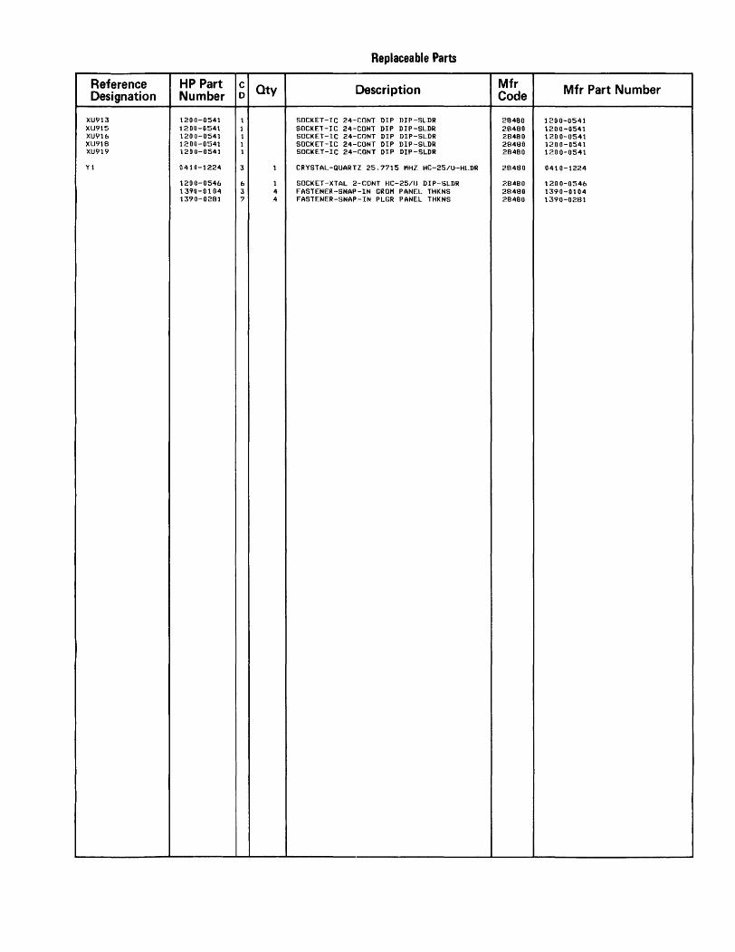
Replaceable Parts
Reference HP Part c Qty Description Mfr Mfr Part Number Designation Number 0 Code
XU913 1200-0541 1 SOCKET-IC 24-·CONT DIP DIP-··SL.DR 28480 1::'.00-0541 XlJ915 1200-0541 1 SOCKET-IC 24-CONT DIP DIP-SLDR 28480 1200-0541 XU916 12011-0541 1 SOCKET-Ie 24-·CONT DIP DIP--SLDR 28480 1200-0541 XlJ918 1;;!'OO-0541 1 SOCKET-IC 24-CONT DIP DIP-SLDR 28480 1200-0541 XIJ919 12011-0541 1 SOCKET-IC 24-CONT DIP DIP--SLDR 28480 1200-0541
Y"1 04111-1224 3 1 CRYSTAL-QUARTZ 25.7715 MHZ HC-25/U-HLDR 28480 0410·-1224
1200-0546 6 1 SOCKET-XTAL 2-CONT HC-25/1J DIP-SLDR 28480 1 ;~o 0-0546 1390-0104 3 4 FASTENER-SNAP-IN GROM PANEL THKNS 28480 1390-0104 1390-0281 7 4 FASTENER-SNAP-IN PLGR PANEL HIKNS 28480 1390-0281


2620
MFR NO,
SO~:j4:i,
00000 01121 012'1::; O~i508 0471::; 0'7263 11961 16299 27014 21H80 3L58:':; 34371 5628<;'
MAN U rAe T U R E R S
MANUFACTURER NAME
NIPPON ELECTRIC CO ANY SATISFACTORY SUPPLIER ALLEN-BRADLEY CO TEXAS INSTR INC SEMICOND CMPNT DIU GE CO SEMICONDUCTOR PROD DEPT MOTOROLA SEMICONDUCTOR PRODUCTS FAIRCHILD SEMICONDUCTOR DIU SEMICON INC CORNING GLASS WKS COMPONENT DIU NATIONAL SEMICONDUCTOR CORP HEWLETT-PACKARD CO CORPORATE HQ RCA CORP SOLID STATE DIU HARRIS SEMI CON DIU HARRIS-INTERTYPE SPRAGUE ELECTRIC CO
COD E L I !3 T AS OF 12101/81 PAGE
ZIP ADDRESS CODE
TOKYO JP
MILWAUKEE WI 53204 DALLAS TX 75222 AUBURN NY 13201 PHOENIX AZ 85008 MOUNTAIN VIEW CA 94042 BURLINGTON MA 01803 RALEIGH NC 27604 SANTA CLARA CA 95051 PALO ALTO CA 94304 SOMERVILLE NJ HELBOURNE FL 32901 NORTH ADAMS PIA 01247
