datasheet amd athlon ii
TRANSCRIPT

8/13/2019 Datasheet AMD Athlon II
http://slidepdf.com/reader/full/datasheet-amd-athlon-ii 1/88
Preliminary Information
AMD AthlonProcessor Model 4
Data Sheet
Publication # 23792 Rev: K
Issue Date: November 2001
TM

8/13/2019 Datasheet AMD Athlon II
http://slidepdf.com/reader/full/datasheet-amd-athlon-ii 2/88
Preliminary Information
Trademarks
AMD, the AMD Arrow logo, AMD Athlon, AMD Duron, and combinations thereof, and 3DNow! are trademarksof Advanced Micro Devices, Inc.
HyperTransport is a trademark of the HyperTransport Technology Consortium.
MMX is a trademark of Intel Corporation.
Other product names used in this publication are for identification purposes only and may be trademarks of
their respective companies.
© 2000, 2001 Advanced Micro Devices, Inc. All rights reserved.
The contents of this document are provided in connection with Advanced
Micro Devices, Inc. (“AMD”) products. AMD makes no representations or war-
ranties with respect to the accuracy or completeness of the contents of this
publication and reserves the right to make changes to specifications and prod-
uct descriptions at any time without notice. No license, whether express,
implied, arising by estoppel or otherwise, to any intellectual property rights is
granted by this publication. Except as set forth in AMD’s Standard Terms and
Conditions of Sale, AMD assumes no liability whatsoever, and disclaims any
express or implied warranty, relating to its products including, but not limited
to, the implied warranty of merchantability, fitness for a particular purpose,or infringement of any intellectual property right.
AMD’s products are not designed, intended, authorized or warranted for use
as components in systems intended for surgical implant into the body, or in
other applications intended to support or sustain life, or in any other applica-
tion in which the failure of AMD’s product could create a situation where per-
sonal injury, death, or severe property or environmental damage may occur.
AMD reserves the right to discontinue or make changes to its products at any

8/13/2019 Datasheet AMD Athlon II
http://slidepdf.com/reader/full/datasheet-amd-athlon-ii 3/88
Contents iii
23792K—November 2001 AMD Athlon™ Processor Model 4 Data Sheet
Preliminary Information
Contents
Revision History. . . . . . . . . . . . . . . . . . . . . . . . . . . . . . . . . . . . . . xi
1 Overview . . . . . . . . . . . . . . . . . . . . . . . . . . . . . . . . . . . . . . . . . . . . 1
1.1 AMD Athlon™ Processor Model 4 Microarchitecture
Summary . . . . . . . . . . . . . . . . . . . . . . . . . . . . . . . . . . . . . . . . . . . 2
2 Interface Signals . . . . . . . . . . . . . . . . . . . . . . . . . . . . . . . . . . . . . 5
2.1 Overview . . . . . . . . . . . . . . . . . . . . . . . . . . . . . . . . . . . . . . . . . . . 5
2.2 Signaling Technology . . . . . . . . . . . . . . . . . . . . . . . . . . . . . . . . . 5
2.3 Push-Pull (PP) Drivers . . . . . . . . . . . . . . . . . . . . . . . . . . . . . . . . 6
2.4 AMD Athlon System Bus Signals . . . . . . . . . . . . . . . . . . . . . . . 6
3 Logic Symbol Diagram . . . . . . . . . . . . . . . . . . . . . . . . . . . . . . . . 7
4 Power Management . . . . . . . . . . . . . . . . . . . . . . . . . . . . . . . . . . 9
4.1 Power Management States . . . . . . . . . . . . . . . . . . . . . . . . . . . . 9
Working State . . . . . . . . . . . . . . . . . . . . . . . . . . . . . . . . . . . . . . 10
Halt State . . . . . . . . . . . . . . . . . . . . . . . . . . . . . . . . . . . . . . . . . . 10
Stop Grant States. . . . . . . . . . . . . . . . . . . . . . . . . . . . . . . . . . . . 10
Probe State. . . . . . . . . . . . . . . . . . . . . . . . . . . . . . . . . . . . . . . . . 11
4.2 Connect and Disconnect Protocol . . . . . . . . . . . . . . . . . . . . . . 12
Connect Protocol . . . . . . . . . . . . . . . . . . . . . . . . . . . . . . . . . . . . 12
Connect State Diagram. . . . . . . . . . . . . . . . . . . . . . . . . . . . . . . 15
4.3 Clock Control . . . . . . . . . . . . . . . . . . . . . . . . . . . . . . . . . . . . . . 17
5 Thermal Design . . . . . . . . . . . . . . . . . . . . . . . . . . . . . . . . . . . . . 196 CPUID Support . . . . . . . . . . . . . . . . . . . . . . . . . . . . . . . . . . . . . 21
7 Electrical Data . . . . . . . . . . . . . . . . . . . . . . . . . . . . . . . . . . . . . . 23
7.1 Conventions . . . . . . . . . . . . . . . . . . . . . . . . . . . . . . . . . . . . . . . 23
7.2 Interface Signal Groupings . . . . . . . . . . . . . . . . . . . . . . . . . . . 23
7.3 Voltage Identification (VID[4:0]) . . . . . . . . . . . . . . . . . . . . . . 24
7.4 Frequency Identification (FID[3:0]) . . . . . . . . . . . . . . . . . . . . 24
7.5 VCCA AC and DC Characteristics . . . . . . . . . . . . . . . . . . . . . 25
7.6 Decoupling . . . . . . . . . . . . . . . . . . . . . . . . . . . . . . . . . . . . . . . . 25
7.7 Operating Ranges . . . . . . . . . . . . . . . . . . . . . . . . . . . . . . . . . . . 25
7.8 Absolute Ratings . . . . . . . . . . . . . . . . . . . . . . . . . . . . . . . . . . . 26
7.9 VCC_CORE Voltage and Current . . . . . . . . . . . . . . . . . . . . . . 27
7.10 SYSCLK and SYSCLK# AC and DC Characteristics . . . . . . 28
7.11 AMD Athlon System Bus AC and DC Characteristics . . . . . 30
7.12 General AC and DC Characteristics . . . . . . . . . . . . . . . . . . . . 32
7.13 APIC Pins AC and DC Characteristics . . . . . . . . . . . . . . . . . . 34

8/13/2019 Datasheet AMD Athlon II
http://slidepdf.com/reader/full/datasheet-amd-athlon-ii 4/88
iv Contents
AMD Athlon™ Processor Model 4 Data Sheet 23792K—November 2001
Preliminary Information
8 Signal and Power-Up Requirements . . . . . . . . . . . . . . . . . . . . 35
8.1 Power-Up Requirements . . . . . . . . . . . . . . . . . . . . . . . . . . . . . 35
Signal Sequence and Timing Description . . . . . . . . . . . . . . . . 35
Clock Multiplier Selection (FID[3:0]) . . . . . . . . . . . . . . . . . . . 37
Serial Initialization Packet (SIP) Protocol . . . . . . . . . . . . . . . 388.2 Processor Warm Reset Requirements . . . . . . . . . . . . . . . . . . 38
The AMD Athlon Processor Model 4 and Northbridge
Reset Pins. . . . . . . . . . . . . . . . . . . . . . . . . . . . . . . . . . . . . . . . . . 38
9 Mechanical Data . . . . . . . . . . . . . . . . . . . . . . . . . . . . . . . . . . . . 39
9.1 Introduction . . . . . . . . . . . . . . . . . . . . . . . . . . . . . . . . . . . . . . . 39
9.2 Die Loading . . . . . . . . . . . . . . . . . . . . . . . . . . . . . . . . . . . . . . . . 39
9.3 AMD Athlon Processor Model 4 CPGA Package
Dimensions . . . . . . . . . . . . . . . . . . . . . . . . . . . . . . . . . . . . . . . . 40
10 Pin Descriptions . . . . . . . . . . . . . . . . . . . . . . . . . . . . . . . . . . . . 43
10.1 Pin Diagram and Pin Name Abbreviations . . . . . . . . . . . . . . 4310.2 Pin List . . . . . . . . . . . . . . . . . . . . . . . . . . . . . . . . . . . . . . . . . . . 52
10.3 Detailed Pin Descriptions . . . . . . . . . . . . . . . . . . . . . . . . . . . . 60
A20M# Pin . . . . . . . . . . . . . . . . . . . . . . . . . . . . . . . . . . . . . . . . . 60
AMD Pin. . . . . . . . . . . . . . . . . . . . . . . . . . . . . . . . . . . . . . . . . . . 60
AMD Athlon System Bus Pins . . . . . . . . . . . . . . . . . . . . . . . . . 60
Analog Pin . . . . . . . . . . . . . . . . . . . . . . . . . . . . . . . . . . . . . . . . . 60
APIC Pins, PICCLK, PICD[1:0]# . . . . . . . . . . . . . . . . . . . . . . . 60
CLKFWDRST Pin . . . . . . . . . . . . . . . . . . . . . . . . . . . . . . . . . . . 60
CLKIN, RSTCLK (SYSCLK) Pins. . . . . . . . . . . . . . . . . . . . . . . 60
CONNECT Pin . . . . . . . . . . . . . . . . . . . . . . . . . . . . . . . . . . . . . . 60
COREFB and COREFB# Pins. . . . . . . . . . . . . . . . . . . . . . . . . . 61
CPU_PRESENCE# Pin . . . . . . . . . . . . . . . . . . . . . . . . . . . . . . . 61DBRDY and DBREQ# Pins . . . . . . . . . . . . . . . . . . . . . . . . . . . . 61
FERR Pin . . . . . . . . . . . . . . . . . . . . . . . . . . . . . . . . . . . . . . . . . . 61
FID[3:0] Pins . . . . . . . . . . . . . . . . . . . . . . . . . . . . . . . . . . . . . . . 61
FLUSH# Pin . . . . . . . . . . . . . . . . . . . . . . . . . . . . . . . . . . . . . . . . 63
IGNNE# Pin . . . . . . . . . . . . . . . . . . . . . . . . . . . . . . . . . . . . . . . . 63
INIT# Pin . . . . . . . . . . . . . . . . . . . . . . . . . . . . . . . . . . . . . . . . . . 63
INTR Pin. . . . . . . . . . . . . . . . . . . . . . . . . . . . . . . . . . . . . . . . . . . 63
JTAG Pins. . . . . . . . . . . . . . . . . . . . . . . . . . . . . . . . . . . . . . . . . . 63
K7CLKOUT and K7CLKOUT# Pins. . . . . . . . . . . . . . . . . . . . . 63
Key Pins . . . . . . . . . . . . . . . . . . . . . . . . . . . . . . . . . . . . . . . . . . . 63
NC Pins. . . . . . . . . . . . . . . . . . . . . . . . . . . . . . . . . . . . . . . . . . . . 63
NMI Pin . . . . . . . . . . . . . . . . . . . . . . . . . . . . . . . . . . . . . . . . . . . 63
PGA Orientation Pins . . . . . . . . . . . . . . . . . . . . . . . . . . . . . . . . 63
PLL Bypass and Test Pins. . . . . . . . . . . . . . . . . . . . . . . . . . . . . 64
PWROK Pin . . . . . . . . . . . . . . . . . . . . . . . . . . . . . . . . . . . . . . . . 64
SADDIN[1:0]# and SADDOUT[1:0]# Pins. . . . . . . . . . . . . . . . 64
Scan Pins . . . . . . . . . . . . . . . . . . . . . . . . . . . . . . . . . . . . . . . . . . 64
SMI# Pin. . . . . . . . . . . . . . . . . . . . . . . . . . . . . . . . . . . . . . . . . . . 64
STPCLK# Pin . . . . . . . . . . . . . . . . . . . . . . . . . . . . . . . . . . . . . . . 64
SYSCLK and SYSCLK# Pins . . . . . . . . . . . . . . . . . . . . . . . . . . 64

8/13/2019 Datasheet AMD Athlon II
http://slidepdf.com/reader/full/datasheet-amd-athlon-ii 5/88
Contents v
23792K—November 2001 AMD Athlon™ Processor Model 4 Data Sheet
Preliminary Information
SYSVREFMODE Pin. . . . . . . . . . . . . . . . . . . . . . . . . . . . . . . . . 64
VCCA Pin . . . . . . . . . . . . . . . . . . . . . . . . . . . . . . . . . . . . . . . . . . 65
VID[4:0] Pins . . . . . . . . . . . . . . . . . . . . . . . . . . . . . . . . . . . . . . . 65
VREFSYS Pin . . . . . . . . . . . . . . . . . . . . . . . . . . . . . . . . . . . . . . 66
ZN, VCC_Z, ZP, and VSS_Z Pins . . . . . . . . . . . . . . . . . . . . . . . 66
11 Ordering Information . . . . . . . . . . . . . . . . . . . . . . . . . . . . . . . . 71
Standard AMD Athlon Processor Model 4 Products . . . . . . . . . . . . . 71
Appendix A Conventions and Abbreviations . . . . . . . . . . . . . . . . . . 73
Signals and Bits . . . . . . . . . . . . . . . . . . . . . . . . . . . . . . . . . . . . . . . . . . . 73
Data Terminology . . . . . . . . . . . . . . . . . . . . . . . . . . . . . . . . . . . . . . . . . 74
Abbreviations and Acronyms. . . . . . . . . . . . . . . . . . . . . . . . . . . . . . . . 75

8/13/2019 Datasheet AMD Athlon II
http://slidepdf.com/reader/full/datasheet-amd-athlon-ii 6/88
vi Contents
AMD Athlon™ Processor Model 4 Data Sheet 23792K—November 2001
Preliminary Information

8/13/2019 Datasheet AMD Athlon II
http://slidepdf.com/reader/full/datasheet-amd-athlon-ii 7/88
List of Figures vii
23792K—November 2001 AMD Athlon™ Processor Model 4 Data Sheet
Preliminary Information
List of Figures
Figure 1. Typical AMD Athlon™ Processor Model 4 SystemBlock Diagram . . . . . . . . . . . . . . . . . . . . . . . . . . . . . . . . . . . . . . . . 3
Figure 2. Logic Symbol Diagram. . . . . . . . . . . . . . . . . . . . . . . . . . . . . . . . . . 7
Figure 3. AMD Athlon Processor Model 4 Power Management
States . . . . . . . . . . . . . . . . . . . . . . . . . . . . . . . . . . . . . . . . . . . . . . . . 9
Figure 4. Example of an AMD Athlon System Bus Disconnect
Sequence . . . . . . . . . . . . . . . . . . . . . . . . . . . . . . . . . . . . . . . . . . . . 13
Figure 5. Exiting Stop Grant State/Bus Reconnect Sequence . . . . . . . . . 14
Figure 6. Northbridge Connect State Diagram . . . . . . . . . . . . . . . . . . . . . 15
Figure 7. Processor Connect State Diagram . . . . . . . . . . . . . . . . . . . . . . . 16
Figure 8. SYSCLK and SYSCLK# Differential Clock Signals . . . . . . . . . 28
Figure 9. SYSCLK Waveform . . . . . . . . . . . . . . . . . . . . . . . . . . . . . . . . . . . 29
Figure 10. Signal Relationship Requirements During Power-Up
Sequence . . . . . . . . . . . . . . . . . . . . . . . . . . . . . . . . . . . . . . . . . . . . 35
Figure 11. AMD Athlon Processor Model 4 CPGA Package. . . . . . . . . . . . 41
Figure 12. AMD Athlon Processor Model 4 Pin Diagram—
Topside View . . . . . . . . . . . . . . . . . . . . . . . . . . . . . . . . . . . . . . . . 44
Figure 13. AMD Athlon Processor Model 4 Pin Diagram—
Bottomside View. . . . . . . . . . . . . . . . . . . . . . . . . . . . . . . . . . . . . . 45
Figure 14. PGA OPN Example for the AMD Athlon Processor
Model 4 . . . . . . . . . . . . . . . . . . . . . . . . . . . . . . . . . . . . . . . . . . . . . 71

8/13/2019 Datasheet AMD Athlon II
http://slidepdf.com/reader/full/datasheet-amd-athlon-ii 8/88
viii List of Figures
AMD Athlon™ Processor Model 4 Data Sheet 23792K—November 2001
Preliminary Information

8/13/2019 Datasheet AMD Athlon II
http://slidepdf.com/reader/full/datasheet-amd-athlon-ii 9/88
List of Tables ix
23792K—November 2001 AMD Athlon™ Processor Model 4 Data Sheet
Preliminary Information
List of Tables
Table 1. Thermal Design Power. . . . . . . . . . . . . . . . . . . . . . . . . . . . . . . . . 19
Table 2. Interface Signal Groupings . . . . . . . . . . . . . . . . . . . . . . . . . . . . . 23
Table 3. VID[4:0] DC Characteristics . . . . . . . . . . . . . . . . . . . . . . . . . . . . 24
Table 4. FID[3:0] DC Characteristics . . . . . . . . . . . . . . . . . . . . . . . . . . . . 24
Table 5. VCCA AC and DC Characteristics . . . . . . . . . . . . . . . . . . . . . . . 25
Table 6. Operating Ranges. . . . . . . . . . . . . . . . . . . . . . . . . . . . . . . . . . . . . 25
Table 7. Absolute Ratings . . . . . . . . . . . . . . . . . . . . . . . . . . . . . . . . . . . . . 26
Table 8. VCC_CORE Voltage and Current. . . . . . . . . . . . . . . . . . . . . . . . 27
Table 9. SYSCLK and SYSCLK# DC Characteristics . . . . . . . . . . . . . . . 28
Table 10. SYSCLK and SYSCLK# AC Characteristics . . . . . . . . . . . . . . . 29
Table 11. AMD Athlon™ System Bus DC Characteristics . . . . . . . . . . . . 30
Table 12. AMD Athlon System Bus AC Characteristics . . . . . . . . . . . . . . 31
Table 13. General AC and DC Characteristics . . . . . . . . . . . . . . . . . . . . . . 32
Table 14. APIC Pins AC and DC Characteristics . . . . . . . . . . . . . . . . . . . . 34
Table 15. CPGA Mechanical Loading . . . . . . . . . . . . . . . . . . . . . . . . . . . . . 39
Table 16. Dimensions for the AMD Athlon Processor Model 4
CPGA Package . . . . . . . . . . . . . . . . . . . . . . . . . . . . . . . . . . . . . . . 40
Table 17. Pin Name Abbreviations . . . . . . . . . . . . . . . . . . . . . . . . . . . . . . . 46
Table 18. Cross-Reference by Pin Location . . . . . . . . . . . . . . . . . . . . . . . . 52Table 19. FID[3:0] Clock Multiplier Encodings . . . . . . . . . . . . . . . . . . . . . 62
Table 20. VID[4:0] Code to Voltage Definition . . . . . . . . . . . . . . . . . . . . . 66
Table 21. Abbreviations . . . . . . . . . . . . . . . . . . . . . . . . . . . . . . . . . . . . . . . . 75
Table 22. Acronyms. . . . . . . . . . . . . . . . . . . . . . . . . . . . . . . . . . . . . . . . . . . . 76

8/13/2019 Datasheet AMD Athlon II
http://slidepdf.com/reader/full/datasheet-amd-athlon-ii 10/88
x List of Tables
AMD Athlon™ Processor Model 4 Data Sheet 23792K—November 2001
Preliminary Information

8/13/2019 Datasheet AMD Athlon II
http://slidepdf.com/reader/full/datasheet-amd-athlon-ii 11/88
Revision History xi
23792K—November 2001 AMD Athlon™ Processor Model 4 Data Sheet
Preliminary Information
Revision History
Date Rev Description
November 2001 K
This revision of the AMD Athlon™ Processor Model 4 Data Sheet covers changes sinceSeptember 2001 that include the following:
■ In Chapter 5, revised Table 1, “Thermal Design Power,” on page 19
■ In Chapter 7, revised Table 8, “VCC_CORE Voltage and Current,” on page 27
■ In Chapter 11, revised Figure 14, "PGA OPN Example for the AMD Athlon™ Processor Model4‚" on page 71
September 2001 J
This revision of the 1400 MHz AMD Athlon™ Processor Model 4 covers changes since June2001 that include the following:
In Chapter 9, added Table 16, “Dimensions for the AMD Athlon™ Processor Model 4 CPGAPackage,” on page 40, and revised Figure 11, "AMD Athlon™ Processor Model 4 CPGAPackage‚" on page 41.
June 2001 I
This revision is for the 1400 MHz AMD Athlon™ Processor Model 4 and covers changes sinceMarch 2001 that include the following:
■ In Chapter 4, included APIC information in “Halt State” on page 10 and “Stop Grant States”on page 10
■ In Chapter 5, updated Table 1, “Thermal Design Power,” on page 19
■ In Chapter 7, updated Table 8, “VCC_CORE Voltage and Current,” on page 27
■ In Chapter 10, revised description of “FERR Pin” on page 61 and in Table 18 on page 52
March 2001 H
This revision is for the 1333 MHz speed grade and covers changes since October 2000.
■ In Chapter 1, revised description on the AMD Athlon™ system bus.■ In Chapter 4, revised Figure 3, "AMD Athlon™ Processor Model 4 Power Management
States‚" on page 9
■ In Chapter 5, updated Table 1, “Thermal Design Power,” on page 20
■ In Chapter 7, updated IoL specification to 12 mA in Table 14, “APIC Pins AC and DCCharacteristics,” on page 34. Updated Table 8, “VCC_CORE Voltage and Current,” on page27, revised Table 10, “SYSCLK and SYSCLK# AC Characteristics,” on page 29, and revisedNote 1 in Table 11, “AMD Athlon™ System Bus DC Characteristics,” on page 30.
■ In Chapter 8, revised description of “Serial Initialization Packet (SIP) Protocol” on page 38
■ In Chapter 10, revised Table 16, “Pin Name Abbreviations,” on page 48, added descriptionof “APIC Pins, PICCLK, PICD[1:0]#” on page 62, and revised description of “AMD Pin” on
page 62
October 2000 G
Added information about the 133 MHz front side bus (FSB) as follows:
■ “AMD Athlon™ Processor Model 4 Microarchitecture Summary” on page 2
■ Table 1, “Thermal Design Power,” on page 19
■ Table 8, “VCC_CORE Voltage and Current,” on page 27
■ Table 10, “SYSCLK and SYSCLK# AC Characteristics,” on page 29
■ Chapter 11, “Ordering Information” on page 71
8/13/2019 Datasheet AMD Athlon II
http://slidepdf.com/reader/full/datasheet-amd-athlon-ii 12/88

8/13/2019 Datasheet AMD Athlon II
http://slidepdf.com/reader/full/datasheet-amd-athlon-ii 13/88
Revision History xiii
23792K—November 2001 AMD Athlon™ Processor Model 4 Data Sheet
Preliminary Information
August 2000 C
Added Table 1, “Thermal Design Power,” on page 21 to Chapter 5, “Thermal Design”.
Revised Chapter 6, “Electrical Data” on page 23 as follows:
■ Added JTAG, APIC, Test, Miscellaneous rows to Table 2, “AMD Athlon™ Processor Model 4Interface Signal Groupings,” on page 23. Reorganized signals into their correct categories.
■ Added “Conventions” on page 23.
■ Revised information in Table 3, “VID[4:0] DC Characteristics,” on page 24.
■ Revised information in Table 4, “FID[3:0] DC Characteristics,” on page 24.
■ Added and revised information in Table 6, “SYSCLK/SYSCLK# AC and DC Characteristics,”on page 23.
■ Revised I VCCA information in Table 5, “VCCA AC and DC Characteristics,” on page 25.
■ Revised maximum values in Table 7, “Absolute Ratings,” on page 26.
■
Revised and reorganized information in Table 8, “VCC_CORE Voltage and Current,” on page27. For thermal information, see Table 1, “Thermal Design Power,” on page 21.
■ Changed VCC_CORE to 1.75V for all speed grades.
Made the following changes in Chapter 7:
■ Changed PLL power source signal name from VDDA to VCCA.
■ Revised Figure 10, “Signal Relationship Requirements during Power-Up Sequence” on page36.
■ Revised the timing requirements in Step 4 on page 37.
■ Revised and reorganized Table 11, “SYSCLK and SYSCLK# AC and DC Characteristics,” onpage 27.
■ Added V CROSS symbol to this table.
Date Rev Description

8/13/2019 Datasheet AMD Athlon II
http://slidepdf.com/reader/full/datasheet-amd-athlon-ii 14/88
xiv Revision History
AMD Athlon™ Processor Model 4 Data Sheet 23792K—November 2001
Preliminary Information
August 2000 C
Revised all figures and information in Chapter 8, “Mechanical Data” on page 41.
Revised Chapter 9, “Pin Descriptions” on page 45 as follows:
■ Changed FERR# to FERR in Figure 15, “AMD Athlon™ Processor Model 4 Pin Diagram—Topside View” on page 46. See “FERR Pin” on page 63 for more information.
■ Revised definition of the Reference column in Table 17, “Socket A Pin Cross-Reference byPin Location,” on page 55 in “Pin List” on page 53.
■ In Table 17, “Socket A Pin Cross-Reference by Pin Location,” on page 55, revisedinformation for the following pin locations:
● N1 (PICCLK), N3 (PIC[0]#), N5 (PIC[1]#), AC7 (VCC_Z), AE33 (SADDIN[5]#), AE35 (SDATAOUTCLK[0]#), AE37 (SDATA[9]#), AG1 (FERR), AJ21 (CLKFWDRST), AJ23(VCCA), AN13 (PLLMON1), AN15 (PLLBYPASSCLK), AN21 (K7CLKOUT#), AN29(SADINN[12]#),
AN31 (SADINN[14]#), AN33 (SDATAINVAL#), AN35 (SADINN[13]#), AN37(SADINN[9]#)
■ Revised information in “K7CLKOUT and K7CLKOUT# Pins” on page 65.
■ Removed all specific resistor values in “Detailed Pin Descriptions” on page 62. For specificimplementation information, see the Motherboard PGA Design Guide, order# 90009.
Revised Chapter 10, “Ordering Information” on page 71.
June 2000 B Initial public release.
Date Rev Description

8/13/2019 Datasheet AMD Athlon II
http://slidepdf.com/reader/full/datasheet-amd-athlon-ii 15/88
Chapter 1 Overview 1
23792K—November 2001 AMD Athlon™ Processor Model 4 Data Sheet
Preliminary Information
1 Overview
The AMD Athlon™ processor model 4 powers the next generation incomputing platforms, delivering compelling performance forcutting-edge applications and an unprecedented computingexperience.
The AMD Athlon processor model 4 wi thperformance-enhancing cache memory is a member of the
AMD Athlon family of processors that are designed to meet thecomputation-intensive requirements of cutting-edge softwareapplications running on high-performance desktop systems,
workstations, and servers.
Delivered in a CPGA package and achieving frequencies of
1.4 GHz (1400 MHz), the AMD Athlon processor model 4delivers the integer, floating-point and 3D multimediaperformance needed for highly demanding applications
running on x86 system platforms. For cutting-edge software
applications, including digital content creation, digital photoediting, digital video, image compression, video encoding for
streaming over the internet, soft DVD, commercial 3D
modeling, workstation-class computer-aided design (CAD),commercial desktop publishing, and speech recognition, the
AMD Athlon processor model 4 del ivers compell ingperformance. It also offers the scalability and reliability that ITmanagers and business users require for enterprise computing.
The AMD Athlon processor model 4 features the
seventh-generation microarchitecture with an integrated L2cache, which supports the growing processor and systembandwidth requirements of emerging software, graphics, I/O,
and memory technologies. The high-speed execution core of theAMD Athlon processor model 4 includes multiple x86instruction decoders, a dual-ported 128-Kbyte split level-one
(L1) cache, a 256-Kbyte on-chip L2 cache, three independentinteger pipelines, three address calculation pipelines, and asuperscalar, fully pipelined, out-of-order, three-way
floating-point engine. The floating-point engine is capable ofdelivering outstanding performance on numerically complexapplications.

8/13/2019 Datasheet AMD Athlon II
http://slidepdf.com/reader/full/datasheet-amd-athlon-ii 16/88
2 Overview Chapter 1
AMD Athlon™ Processor Model 4 Data Sheet 23792K—November 2001
Preliminary Information
The AMD Athlon processor model 4 microarchitectureincorporates enhanced 3DNow!™ technology, a
high-performance cache architecture, and both a 200-MHz,
1.6-Gigabyte per second system bus, and a 266 MHz, 2.1-Gigabyte per second system bus. The AMD Athlon system bus
combines the latest technological advances, such as
point-to-point topology, source-synchronous packet-basedtransfers, and low-voltage signaling, to provide an extremely
powerful, scalable bus for an x86 processor.
The AMD Athlon processor model 4 is binary-compatible withexisting x86 software and backwards compatible withapplications optimized for MMX™ and 3DNow! instructions.
Using a data format and single-instruction multiple-data(SIMD) operations based on the MMX instruction model, the
AMD Athlon processor model 4 can produce as many as four,32-bit, single-precision floating-point results per clock cycle.The enhanced 3DNow! technology implemented in theAMD Athlon processor model 4 includes new integer
multimedia instructions and software-directed data movementinstructions for optimizing such applications as digital contentcreation and streaming video for the internet, as well as new
instructions for digital signal processing (DSP)/communicationsapplications.
1.1 AMD Athlon™ Processor Model 4 Microarchitecture SummaryThe following features summarize the AMD Athlon processor
model 4 microarchitecture:
■ An advanced, superpipelined, superscalar x86 processormicroarchitecture designed for high clock frequencies
■ Multiple x86 instruction decoders
■ Three out-of-order, superscalar, fully pipelinedfloating-point execution units, which execute all x87(floating-point), MMX and 3DNow! instructions
■ Three out-of-order, superscalar, pipelined integer units
■ Three out-of-order, superscalar, pipelined addresscalculation units
■ A 72-entry instruction control unit
■ Advanced dynamic branch prediction
■ Enhanced 3DNow! technology with new instructions toenable improved integer math calculations for speech orvideo encoding and improved data movement for internetplug-ins and other streaming applications

8/13/2019 Datasheet AMD Athlon II
http://slidepdf.com/reader/full/datasheet-amd-athlon-ii 17/88
Chapter 1 Overview 3
23792K—November 2001 AMD Athlon™ Processor Model 4 Data Sheet
Preliminary Information
■ 200-MHz and 266 MHz AMD Athlon system bus (scalablebeyond 400 MHz) enabling leading-edge system bandwidthfor data movement-intensive applications
■ High-performance cache architecture featuring an
integrated 128-Kbyte L1 cache and a 16-way, on-chip256-Kbyte L2 cache for a total of 384-Kbytes of on-chip cache
The AMD Athlon processor model 4 delivers excellent systemperformance in a cost-effective, industry-standard form factor.The AMD Athlon processor model 4 is compatible with
motherboards based on AMD's Socket A. Figure 1 on page 3shows a typical AMD Athlon processor model 4 system blockdiagram.
Figure 1. Typical AMD Athlon™ Processor Model 4 System Block Diagram
DRAM
AGP Bus
Memory Bus
AGP
PCI Bus
LAN SCSI
System
Management
BIOS
ISA Bus
USB
Dual EIDE
AMD Athlon™
Processor
SystemController
(Northbridge)
Peripheral BusController
(Southbridge)

8/13/2019 Datasheet AMD Athlon II
http://slidepdf.com/reader/full/datasheet-amd-athlon-ii 18/88
4 Overview Chapter 1
AMD Athlon™ Processor Model 4 Data Sheet 23792K—November 2001
Preliminary Information

8/13/2019 Datasheet AMD Athlon II
http://slidepdf.com/reader/full/datasheet-amd-athlon-ii 19/88
Chapter 2 Interface Signals 5
23792K—November 2001 AMD Athlon™ Processor Model 4 Data Sheet
Preliminary Information
2 Interface Signals
2.1 Overview
The AMD Athlon™ system bus architecture is designed todeliver unprecedented data movement bandwidth fornext-generation x86 platforms, as well as the high performance
required by enterprise-class application software. The systembus architecture consists of three high-speed channels (aunidirectional processor request channel, a unidirectional
probe channel, and a 72-bit bidirectional data channel),source-synchronous clocking, and a packet-based protocol. Inaddition, the system bus supports several control, clock, and
legacy signals. The interface signals use an impedancecontrolled push-pull low-voltage swing signaling technologycontained within the Socket A socket. For more information,
see “AMD Athlon™ System Bus Signals” on page 6, Chapter 10,“Pin Descriptions” on page 43, and the AMD Athlon™ and
AMD Duron™ System Bus Specification, order# 21902.
2.2 Signaling Technology
The AMD Athlon system bus uses a low-voltage, swing signaling
technology, which has been enhanced to provide larger noisemargins, reduced ringing, and variable voltage levels. Thesignals are push-pull and impedance compensated. The signalinputs use differential receivers, which require a reference
voltage (VREF). The reference signal is used by the receivers todetermine if a signal is asserted or deasserted by the source.Termination resistors are not needed because the driver is
impedance matched to the motherboard and a high impedancereflection is used at the receiver to bring the signal past theinput threshold.
For more information about pins and signals, see Chapter 10,“Pin Descriptions” on page 43.

8/13/2019 Datasheet AMD Athlon II
http://slidepdf.com/reader/full/datasheet-amd-athlon-ii 20/88
6 Interface Signals Chapter 2
AMD Athlon™ Processor Model 4 Data Sheet 23792K—November 2001
Preliminary Information
2.3 Push-Pull (PP) Drivers
The Socket A AMD Athlon processor model 4 supports
Push-Pull (PP) drivers. The system logic configures theAMD Athlon processor model 4 with the configuration
parameter called SysPushPull (1=PP). The impedance of the PP
drivers is set to match the impedance of the motherboard bytwo external resistors connected to the ZN and ZP pins. See
“ZN, VCC_Z, ZP, and VSS_Z Pins” on page 66 for more
information.
2.4 AMD Athlon™ System Bus Signals
The AMD Athlon system bus is a c lock-forwarded,
point-to-point interface with the following three point-to-pointchannels:
■ A 13-bit unidirectional output address/command channel
■ A 13-bit unidirectional input address/command channel
■ A 72-bit bidirectional data channel
For more information, see Chapter 7, “Electrical Data” on page23 and the AMD Athlon™ and AMD Duron™ System Bus Specification, order# 21902.
8/13/2019 Datasheet AMD Athlon II
http://slidepdf.com/reader/full/datasheet-amd-athlon-ii 21/88
Chapter 3 Logic Symbol Diagram 7
23792K—November 2001 AMD Athlon™ Processor Model 4 Data Sheet
Preliminary Information
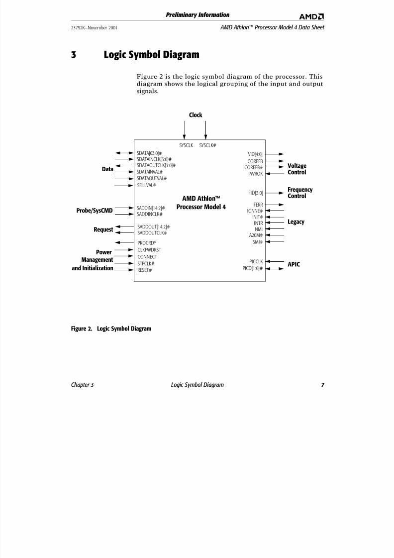
3 Logic Symbol Diagram
Figure 2 is the logic symbol diagram of the processor. Thisdiagram shows the logical grouping of the input and outputsignals.
Figure 2. Logic Symbol Diagram
PICCLK
PICD[1:0]#APIC
SDATA[63:0]#
SDATAINCLK[3:0]#SDATAOUTCLK[3:0]#
Data
SADDIN[14:2]#SADDINCLK#
Probe/SysCMD
SADDOUT[14:2]#SADDOUTCLK#
VID[4:0]
FID[3:0]
A20M#
CLKFWDRST
CONNECT
COREFB COREFB#
FERR IGNNE# INIT# INTR NMI
PROCRDY
PWROK
RESET#
SFILLVAL#
SMI#
STPCLK#
SYSCLK#SYSCLK
Clock
VoltageControl
FrequencyControl
Legacy
Request
AMD Athlon™Processor Model 4
SDATAINVAL#
SDATAOUTVAL#
Power
and Initialization
Management

8/13/2019 Datasheet AMD Athlon II
http://slidepdf.com/reader/full/datasheet-amd-athlon-ii 22/88

8/13/2019 Datasheet AMD Athlon II
http://slidepdf.com/reader/full/datasheet-amd-athlon-ii 23/88
Chapter 4 Power Management 9
23792K—November 2001 AMD Athlon™ Processor Model 4 Data Sheet
Preliminary Information
4 Power Management
4.1 Power Management StatesThe AMD Athlon™ processor model 4 supports low-power Haltand Stop Grant states. These states are used by Advanced
Configuration and Power Interface (ACPI) enabled operatingsystems for processor power management. Figure 3 shows thepower management states of the AMD Athlon processor model
4. The figure includes the ACPI “Cx” naming convention forthese states.
Figure 3. AMD Athlon™ Processor Model 4 Power Management States
C1Halt
C0 Working
Execute HLT
SMI#, INTR, NMI, INIT#, RESET#
I n c o m i n g P r o b e
P r o b e
S e r v i c e d
S T P C L K # a s s e r t e d
S T P C L K # a s s e r t e d 2
S T P C L K # d e a s s e r t e d 3
C2
Stop GrantCache Snoopable
Incoming Probe
Probe ServicedProbeState1
S T P C L K # d e a s s e r t e d
( R e a d P L V L 2 r e g i s t e r
o r t h r o t t l i n g )
C3/S1
Stop GrantCache Not SnoopableSleep
S T P C L K # a s s e r t e d
S T P C L K # d e a s s e r t e d
Legend:Hardware transitions
Software transitions
Legend:Hardware transitions
Software transitionsThe AMD System Bus is connected during the following states:1) The Probe state2) During transitions from Halt state to Stop Grant state3) Stop Grant state to the Halt state
S1
4) The C0 Working state
4
2) During transitions from the Halt state to the Stop Grant state
3) During transitions from Stop Grant state to the Halt state
The AMD Athlon™ System Bus is connected during the following states:

8/13/2019 Datasheet AMD Athlon II
http://slidepdf.com/reader/full/datasheet-amd-athlon-ii 24/88

8/13/2019 Datasheet AMD Athlon II
http://slidepdf.com/reader/full/datasheet-amd-athlon-ii 25/88
Chapter 4 Power Management 11
23792K—November 2001 AMD Athlon™ Processor Model 4 Data Sheet
Preliminary Information
The Stop Grant state is also entered for the S1 system sleepstate based on a write to the SLP_TYP field in the ACPI-defined
power management 1 control register. During the S1 sleep
state, system software ensures no bus master or probe activityoccurs.
After recognizing the assertion of STPCLK#, the AMD Athlon
processor model 4 completes all pending and in-progress buscycles and acknowledges the STPCLK# assertion by issuing aStop Grant special bus cycle to the AMD Athlon system bus.
After the Northbridge disconnects the AMD Athlon system busin response to the Stop Grant special bus cycle, the processorenters a low-power state dictated by the CLK_Ctl register.
During the Stop Grant states, the processor latches INIT#,INTR, NMI, and SMI#, or a local APIC interrupt message if they
are asserted.
The Stop Grant state is exited upon the deassertion ofSTPCLK# or the assertion of RESET#. When STPCLK# is
deasserted, the processor initiates a connection of theAMD Athlon system bus if it is disconnected. After theprocessor enters the Working state, any pending interrupts are
recognized and serviced and the processor resumes executionat the instruction boundary where STPCLK# was initiallyrecognized.
If RESET# is sampled asserted during the Stop Grant state, theprocessor returns to the Working state and the reset processbegins.
Probe State The Probe state is entered when the Northbridge initiates an
AMD Athlon system bus connect as required to probe theprocessor. If the processor has been disconnected from the
system bus, the Northbridge must initiate a system bus
connection before it probes the processor to snoop the caches ofthe processor . The processor responds to a probe cycle in the
Probe state in the same way it does during the Working state.
When the probe has been serviced, the processor returns to thesame state as when it entered the Probe state (Halt or StopGrant state). Once in the Halt or Stop Grant state, a low-power
state is only achieved if the Northbridge initiates adisconnection from the system bus.
8/13/2019 Datasheet AMD Athlon II
http://slidepdf.com/reader/full/datasheet-amd-athlon-ii 26/88
12 Power Management Chapter 4
AMD Athlon™ Processor Model 4 Data Sheet 23792K—November 2001
Preliminary Information
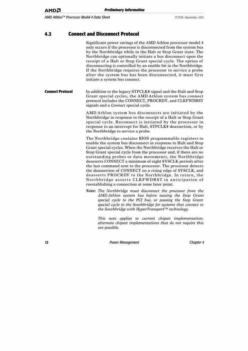
4.2 Connect and Disconnect Protocol
Significant power savings of the AMD Athlon processor model 4
only occurs if the processor is disconnected from the system busby the Northbridge while in the Halt or Stop Grant state. The
Northbridge can optionally initiate a bus disconnect upon the
receipt of a Halt or Stop Grant special cycle. The option ofdisconnecting is controlled by an enable bit in the Northbridge.
If the Northbridge requires the processor to service a probe
after the system bus has been disconnected, it must firstinitiate a system bus connect.
Connect Protocol In addition to the legacy STPCLK# signal and the Halt and StopGrant special cycles, the AMD Athlon system bus connect
protocol includes the CONNECT, PROCRDY, and CLKFWDRSTsignals and a Connect special cycle.
AMD Athlon system bus disconnects are initiated by the
Northbridge in response to the receipt of a Halt or Stop Grantspecial cycle. Reconnect is initiated by the processor inresponse to an interrupt for Halt, STPCLK# deassertion, or by
the Northbridge to service a probe.
The Northbridge contains BIOS programmable registers to
enable the system bus disconnect in response to Halt and StopGrant special cycles. When the Northbridge receives the Halt orStop Grant special cycle from the processor and, if there are no
outstanding probes or data movements, the Northbridgedeasserts CONNECT a minimum of eight SYSCLK periods afterthe last command sent to the processor. The processor detects
the deassertion of CONNECT on a rising edge of SYSCLK, anddeasserts PROCRDY to the Northbridge. In return, theNorthbridge asserts CLKFWDRST in anticipation of
reestablishing a connection at some later point.
Note: The Northbridge must disconnect the processor from the AMD Athlon system bus before issuing the Stop Grant
special cycle to the PCI bus, or passing the Stop Grant special cycle to the Southbridge for systems that connect tothe Southbridge with HyperTransport™ technology.
This note applies to current chipset implementation:alternate chipset implementations that do not require this
are possible.

8/13/2019 Datasheet AMD Athlon II
http://slidepdf.com/reader/full/datasheet-amd-athlon-ii 27/88
Chapter 4 Power Management 13
23792K—November 2001 AMD Athlon™ Processor Model 4 Data Sheet
Preliminary Information
Note: In response to Halt special cycles, the Northbridge passes the Halt special cycle to the PCI bus or Southbridge
immediately.
The processor can receive an interrupt after it sends a Haltspecial cycle, or STPCLK# deassertion after it sends a StopGrant special cycle to the Northbridge but before the
disconnect actually occurs. In this case, the processor sends theConnect special cycle to the Northbridge, rather thancontinuing with the disconnect sequence. In response to the
Connect special cycle, the Northbridge cancels the disconnectrequest.
The system is required to assert the CONNECT signal beforereturning the C-bit for the connect special cycle (assuming
CONNECT has been deasserted). For more information, see the AMD Athlon™ and AMD Duron™ System Bus Specification,order# 21902 for the definition of the C-bit and the Connectspecial cycle.
Figure 4 shows the sequence of events from a Northbridge
perspective, which leads to disconnecting the processor fromthe AMD Athlon system bus and placing the processor in theStop Grant state.
Figure 4. Example of an AMD Athlon™ System Bus Disconnect Sequence
The following sequence of events describes how the processor isplaced in the Stop Grant state when bus disconnect is enabledwithin the Northbridge:
1. The Southbridge asserts STPCLK# to place the processor in
the Stop Grant state.
2. When the processor recognizes STPCLK# asserted, theprocessor enters the Stop Grant State, then issues a Stop
Grant special cycle on the AMD Athlon system bus.
Stop Grant
Stop Grant
STPCLK#
CONNECT
PROCRDY
CLKFWDRST
PCI Bus
System Bus

8/13/2019 Datasheet AMD Athlon II
http://slidepdf.com/reader/full/datasheet-amd-athlon-ii 28/88
14 Power Management Chapter 4
AMD Athlon™ Processor Model 4 Data Sheet 23792K—November 2001
Preliminary Information
3. When the Stop Grant special cycle is received by theNorthbridge and no probe traffic is pending, the
Northbridge deasserts CONNECT, initiating a bus
disconnect to the processor.
4. The processor responds to the Northbridge by deassertingPROCRDY, acknowledging the bus disconnect request.
5. The Northbridge asserts CLKFWDRST to complete the busdisconnect sequence.
6. After the processor is disconnected from the bus, theNorthbridge passes the Stop Grant special cycle to theSouthbridge.
Figure 5 shows the signal sequence of events that take the
processor out of the Stop Grant state, reconnect the processorto the AMD Athlon system bus, and put the processor into theWorking state.
Figure 5. Exiting Stop Grant State/Bus Reconnect Sequence
The following sequence of events removes the processor from
the Stop Grant state and reconnects it to the AMD Athlon
system bus:
1. The Southbridge deasserts STPCLK# in response to aresume event.
2. When the processor recognizes STPCLK# deassertion, itasserts PROCRDY, notifying the Northbridge to reconnect
to the bus.
3. The Northbridge asserts CONNECT.
4. The Northbridge finally deasserts CLKFWDRST, whichsynchronizes the forwarded clocks between the processor
and the Northbridge.
STPCLK#
PROCRDY
CONNECT
CLKFWDRST

8/13/2019 Datasheet AMD Athlon II
http://slidepdf.com/reader/full/datasheet-amd-athlon-ii 29/88

8/13/2019 Datasheet AMD Athlon II
http://slidepdf.com/reader/full/datasheet-amd-athlon-ii 30/88
16 Power Management Chapter 4
AMD Athlon™ Processor Model 4 Data Sheet 23792K—November 2001
Preliminary Information
Figure 7. Processor Connect State Diagram
Condition
1CONNECT is deasserted by the Northbridge (for apreviously sent Halt or Stop Grant special cycle).
2 Processor receives a wake-up event and must cancel the disconnect request.
3 Deassert PROCRDY and slow down internal clocks.
4Processor wake-up event or CONNECT asserted byNorthbridge.
5 CLKFWDRST is deasserted by the Northbridge.
6Forward clocks start three SYSCLK periods afterCLKFWDRST is deasserted.
Action
A CLKFWDRST is asserted by the Northbridge.
B Issue a CONNECT special cycle.*
C Return internal clocks to full speed and assertPROCRDY
* The Connect special cycle is only issued after a processor wake-up event (interrupt or STPCLK#deassertion) occurs. If the AMD Athlon system bus
is connected so the Northbridge can probe the processor a Connect special cycle is not issued atthat time (it is only issued after a subsequent
processor wake-up event).
Connect
DisconnectPending
Disconnect
Connect
Pending 1Connect
Pending 2
1
3/A
4/C
5
6/B
2/B

8/13/2019 Datasheet AMD Athlon II
http://slidepdf.com/reader/full/datasheet-amd-athlon-ii 31/88
Chapter 4 Power Management 17
23792K—November 2001 AMD Athlon™ Processor Model 4 Data Sheet
Preliminary Information
4.3 Clock Control
The processor implements a Clock Control (CLK_Ctl) MSR
(address C001_001Bh) that determines the internal clockdivisor when the AMD Athlon system bus is disconnected.
Refer to the AMD Athlon™ and AMD Duron™ Processors BIOS,
Software, and Debug Developers Guide , order# 21656, for moredetails on the CLK_Ctl register.

8/13/2019 Datasheet AMD Athlon II
http://slidepdf.com/reader/full/datasheet-amd-athlon-ii 32/88
18 Power Management Chapter 4
AMD Athlon™ Processor Model 4 Data Sheet 23792K—November 2001
Preliminary Information

8/13/2019 Datasheet AMD Athlon II
http://slidepdf.com/reader/full/datasheet-amd-athlon-ii 33/88
Chapter 5 Thermal Design 19
23792K—November 2001 AMD Athlon™ Processor Model 4 Data Sheet
Preliminary Information
5 Thermal Design
For information about thermal design for the AMD Athlon™processor model 4, including layout and airflow considerations,see the AMD Thermal, Mechanical, and Chassis Cooling Design
Guide , order# 23794, and the cool ing guidel ines onwww.amd.com.
Table 1 shows the thermal design power. The thermal designpower represents the maximum sustained power dissipatedwhile executing publicly available software or instruction
sequences under normal system operation at nominalVCC_CORE. Thermal solutions must monitor the processortemperature to prevent the processor from exceeding its
maximum die temperature.
Table 1. Thermal Design Power
Frequency(MHz)
Nominal Voltage
Maximum ThermalPower
Typical ThermalPower
Max DieTemperature
900
1.75 V
51.0 W 45.8 W
90ºC950 53.1 W 47.6 W
1000 55.1 W 49.5 W
1100 60.3 W 54.1 W
1133 62.1 W 55.7 W
95ºC
1200 65.7 W 58.9 W
1266 66.9 W 60.1 W
1300 68.3 W 61.3 W
1333 69.8 W 62.6 W
1400 72.1 W 64.7 W

8/13/2019 Datasheet AMD Athlon II
http://slidepdf.com/reader/full/datasheet-amd-athlon-ii 34/88
20 Thermal Design Chapter 5
AMD Athlon™ Processor Model 4 Data Sheet 23792K—November 2001
Preliminary Information

8/13/2019 Datasheet AMD Athlon II
http://slidepdf.com/reader/full/datasheet-amd-athlon-ii 35/88
Chapter 6 CPUID Support 21
23792K—November 2001 AMD Athlon™ Processor Model 4 Data Sheet
Preliminary Information
6 CPUID Support
AMD Athlon™ processor model 4 version and feature setrecognition can be performed through the use of the CPUIDinstruction that provides complete information about the
processor—vendor, type, name, etc., and its capabilities.Software can make use of this information to accurately tunethe system for maximum performance and benefit to users.
For information on the use of the CPUID instruction, see the AMD Processor Recognition Application Note , order# 20734.

8/13/2019 Datasheet AMD Athlon II
http://slidepdf.com/reader/full/datasheet-amd-athlon-ii 36/88
22 CPUID Support Chapter 6
AMD Athlon™ Processor Model 4 Data Sheet 23792K—November 2001
Preliminary Information

8/13/2019 Datasheet AMD Athlon II
http://slidepdf.com/reader/full/datasheet-amd-athlon-ii 37/88
Chapter 7 Electrical Data 23
23792K—November 2001 AMD Athlon™ Processor Model 4 Data Sheet
Preliminary Information
7 Electrical Data
7.1 Conventions
The conventions used in this chapter are as follows:
■ Current specified as being sourced by the processor is
negative .
■ Current specified as being sunk by the processor is positive .
7.2 Interface Signal Groupings
The electrical data in this chapter is presented separately foreach signal group. Table 2 defines each group and the signals
contained in each group.
Table 2. Interface Signal Groupings
Signal Group Signals Notes
Power VID[4:0], VCC_CORE, VCCA, COREFB, COREFB#
See “Voltage Identification (VID[4:0])”on page 24, “VID[4:0] Pins” on page 65,and “VCCA AC and DC Characteristics”on page 25.
Frequency FID[3:0]
See “Frequency Identification
(FID[3:0])” on page 24 and “FID[3:0]Pins” on page 61.
System ClocksSYSCLK, SYSCLK# (Tied to CLKIN/CLKIN# andRSTCLK/RSTCLK#), PLLBYPASSCLK#, PLLBYPASSCLK
See “SYSCLK and SYSCLK# DCCharacteristics” on page 28.
AMD Athlon™System Bus
SADDIN[14:2]#, SADDOUT[14:2]#, SADDINCLK#,SADDOUTCLK#, SFILLVAL#, SDATAINVAL#,SDATAOUTVAL#, SDATA[63:0]#, SDATAINCLK[3:0]#,SDATAOUTCLK[3:0]#, CLKFWDRST, PROCRDY, CONNECT
See “AMD Athlon™ System Bus AC andDC Characteristics” on page 30.
SouthbridgeRESET#, INTR, NMI, SMI#, INIT#, A20M#, FERR, IGNNE#,STPCLK#, FLUSH#
See “General AC and DCCharacteristics” on page 32.
JTAG TMS, TCK, TRST#, TDI, TDO See “General AC and DCCharacteristics” on page 32.
APIC PICD[1:0]#, PICCLKSee “APIC Pins AC and DCCharacteristics” on page 34 and “APICPins, PICCLK, PICD[1:0]#” on page 60

8/13/2019 Datasheet AMD Athlon II
http://slidepdf.com/reader/full/datasheet-amd-athlon-ii 38/88
24 Electrical Data Chapter 7
AMD Athlon™ Processor Model 4 Data Sheet 23792K—November 2001
Preliminary Information
7.3 Voltage Identification (VID[4:0])
Table 3 shows the VID[4:0] DC characteristics. For more
information, see “VID[4:0] Pins” on page 65.
7.4 Frequency Identification (FID[3:0])
Table 4 shows the FID[3:0] DC characteristics. For moreinformation, see “FID[3:0] Pins” on page 61.
Test
PLLTEST#, PLLMON1, PLLMON2, SCANCLK1, SCANCLK2,
SCANSHIFTEN, SCANINTEVAL, ANALOG
See “General AC and DC
Characteristics” on page 32.
Miscellaneous DBREQ#, DBRDY, PWROK, PLLBYPASS#See “General AC and DCCharacteristics” on page 32.
Table 2. Interface Signal Groupings (continued)
Signal Group Signals Notes
Table 3. VID[4:0] DC Characteristics
Parameter Description Min Max
IOL Output Current Low 16 mA
V OH Output High Voltage 2.625 V *
Note:
* The VID pins must not be pulled above this voltage by an external pullup resistor.
Table 4. FID[3:0] DC Characteristics
Parameter Description Min Max
IOL Output Current Low 16 mA
V OH Output High Voltage 2.625 V *
Note:
* The FID pins must not be pulled above this voltage by an external pullup resistor.

8/13/2019 Datasheet AMD Athlon II
http://slidepdf.com/reader/full/datasheet-amd-athlon-ii 39/88
Chapter 7 Electrical Data 25
23792K—November 2001 AMD Athlon™ Processor Model 4 Data Sheet
Preliminary Information
7.5 VCCA AC and DC Characteristics
Table 5 shows the AC and DC characteristics for VCCA. For
more information, see “VCCA Pin” on page 65.
7.6 Decoupling
See the AMD Athlon™ Processor-Based Motherboard DesignGuide , order# 24363, or contact your local AMD office forinformation about the decoupling required on the motherboard
for use with the AMD Athlon™ processor model 4.
7.7 Operating Ranges
The AMD Athlon processor model 4 is designed to providefunctional operation if the voltage and temperature parameters
are within the limits defined in Table 6.
Table 5. VCCA AC and DC Characteristics
Symbol Parameter Min Nominal Max Units Notes
V VCCA VCCA Pin Voltage 2.25 2.5 2.75 V 1
I VCCA VCCA Pin Current 0 50 mA/GHz 2
Notes:
1. Minimum and maximum voltages are absolute. No transients below minimum nor above maximum voltages are permitted.
2. Measured at 2.5 V.
Table 6. Operating Ranges
Parameter Description Min Nominal Max Notes
VCC_CORE Processor core supply 900-1400 MHz 1.65 V 1.75 V 1.85 V 1
VCC_CORESLEEP Processor core supply in Sleep state 1.2 V 1.3 V 1.4 V 2
TDIE Temperature of processor die 95ºC 3
Notes:
1. For normal operating conditions (nominal VCC_CORE is 1.75 V).
2. Sleep Voltage can be used for the S1 sleep state. For more information see the AMD Athlon™ and AMD Duron™ Processors BIOS,Software, and Debug Developers Guide , order# 21656.
3. Die temperature is 90ºC for frequencies of 1100 MHz and lower.

8/13/2019 Datasheet AMD Athlon II
http://slidepdf.com/reader/full/datasheet-amd-athlon-ii 40/88
26 Electrical Data Chapter 7
AMD Athlon™ Processor Model 4 Data Sheet 23792K—November 2001
Preliminary Information
7.8 Absolute Ratings
The AMD Athlon processor model 4 should not be subjected to
conditions exceeding the absolute ratings listed in Table 7, assuch conditions can adversely affect long-term reliability or
result in functional damage.
Table 7. Absolute Ratings
Parameter Description Min Max
VCC_CORE AMD Athlon™ Processor Model 4 core supply –0.5 V VCC_CORE Max + 0.5 V
VCCA AMD Athlon Processor Model 4 PLL Supply –0.5 V VCCA Max + 0.5 V
V PIN Voltage on any signal pin –0.5 V VCC_CORE Max + 0.5 V
TSTORAGE Storage temperature of processor –40ºC 100ºC
8/13/2019 Datasheet AMD Athlon II
http://slidepdf.com/reader/full/datasheet-amd-athlon-ii 41/88
Chapter 7 Electrical Data 27
23792K—November 2001 AMD Athlon™ Processor Model 4 Data Sheet
Preliminary Information
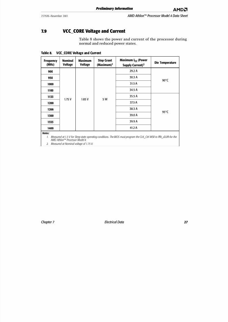
7.9 VCC_CORE Voltage and Current
Table 8 shows the power and current of the processor during
normal and reduced power states.
Table 8. VCC_CORE Voltage and Current
Frequency(MHz)
Nominal Voltage
Maximum Voltage
Stop Grant
(Maximum)1Maximum ICC (Power
Supply Current)2Die Temperature
900
1.75 V 1.85 V 5 W
29.2 A
90°C950 30.3 A
1000 31.5 A
110034.5 A
1133 35.5 A
95°C
1200 37.5 A
1266 38.3 A
1300 39.0 A
1333 39.9 A
1400 41.2 A
Notes:
1. Measured at 1.3 V for Sleep state operating conditions. The BIOS must program the CLK_Ctrl MSR to fff0_d22fh for the AMD Athlon™ Processor Model 4.
2. Measured at Nominal voltage of 1.75 V.

8/13/2019 Datasheet AMD Athlon II
http://slidepdf.com/reader/full/datasheet-amd-athlon-ii 42/88
28 Electrical Data Chapter 7
AMD Athlon™ Processor Model 4 Data Sheet 23792K—November 2001
Preliminary Information
7.10 SYSCLK and SYSCLK# AC and DC Characteristics
Table 9 shows the DC characteristics of the SYSCLK and
SYSCLK# differential clocks. The SYSCLK signal representsCLKIN and RSTCLK tied together while the SYSCLK# signal
represents CLKIN# and RSTCLK# tied together. Figure 8 shows
the waveforms of the SYSCLK and SYSCLK# signals.
Figure 8. SYSCLK and SYSCLK# Differential Clock Signals
Table 9. SYSCLK and SYSCLK# DC Characteristics
Symbol Description Min Max Units
V Threshold-DC Crossing before transition is detected (DC) 400 mV
V Threshold-AC Crossing before transition is detected (AC) 450 mV
ILEAK_P Leakage current through P-channel pullup to VCC_CORE —1 mA
ILEAK_N Leakage current through N-channel pulldown to VSS (Ground) 1 mA
V CROSS Differential signal crossover VCC_CORE/2
+/– 100mV
CPIN Capacitance 4 12 pF
VCROSS VThreshold-DC = 400mV VThreshold-AC = 450mV

8/13/2019 Datasheet AMD Athlon II
http://slidepdf.com/reader/full/datasheet-amd-athlon-ii 43/88
Chapter 7 Electrical Data 29
23792K—November 2001 AMD Athlon™ Processor Model 4 Data Sheet
Preliminary Information
Table 10 shows the SYSCLK/SYSCLK# differential clock ACcharacteristics of the AMD Athlon processor model 4. Figure 9
shows a sample waveform.
Figure 9. SYSCLK Waveform
Table 10. SYSCLK and SYSCLK# AC Characteristics
Symbol Parameter Description Min @ Max @ Units Notes
Clock Frequency 100 133 100 133 MHz
Duty Cycle 30% 30% 70% 70%
t1 Period 10 7.5 ns 1, 2
t2 High Time 1.8 1.05 ns
t3 Low Time 1.8 1.05 ns
t4 Fall Time 2 2 ns
t5 Rise Time 2 2 ns
Period Stability ± 300 ± 300 ps
Notes:
1. Circuitry driving the SYSCLK and SYSCLK# inputs must exhibit a suitably low closed-loop jitter bandwidth to allowthe PLL to track the jitter. The –20 dB attenuation point, as measured into a 10 or 20-pF load must be less than
500 kHz.
2. Circuitry driving the SYSCLK and SYSCLK# inputs can purposely alter the SYSCLK and SYSCLK# period (spread spectrum clock generators). In no cases can the SYSCLK and SYSCLK# period violate the minimum specificationabove. SYSCLK and SYSCLK# inputs can vary from 100% of the specified period to 99% of the specified periodat a maximum rate of 100 kHz.
t5
VCROSS
t2
t3
t4
t1
VThreshold-AC

8/13/2019 Datasheet AMD Athlon II
http://slidepdf.com/reader/full/datasheet-amd-athlon-ii 44/88
30 Electrical Data Chapter 7
AMD Athlon™ Processor Model 4 Data Sheet 23792K—November 2001
Preliminary Information
7.11 AMD Athlon™ System Bus AC and DC Characteristics
Table 11 shows the DC characteristics of the AMD Athlon
system bus used by the AMD Athlon processor model 4.
Table 11. AMD Athlon™ System Bus DC Characteristics
Symbol Parameter Condition Min Max Units Notes
V REF DC Input Reference Voltage(0.5*VCC_CORE)
–50(0.5*VCC_CORE)
+50mV 1
I VREF_LEAK_P V REF Tristate Leakage Pullup V IN = V REF Nominal –100 µ A
I VREF_LEAK_N V REF Tristate Leakage Pulldown V IN = V REF Nominal +100 µ A
V IH Input High Voltage V REF + 200 VCC_CORE +500
mV
V IL Input Low Voltage –500 V REF – 200 mV
V OH Output High Voltage IOUT = –200µ A 0.85*VCC_CORE VCC_CORE+500 mV 2
V OL Output Low Voltage IOUT = 1 mA –500 400 mV 2
ILEAK_P Tristate Leakage Pullup V IN = VSS (Ground) –1 mA
ILEAK_N Tristate Leakage Pulldown V IN = VCC_CORE
Nominal+1 mA
CIN Input Pin Capacitance 4 12 pF 3
Notes:
1. V REF
is nominally set to 50% of VCC_CORE with actual values that are specific to motherboard design implementation. V REF
must becreated with a sufficiently accurate DC source and a sufficiently quiet AC response to adhere to the ± 50 mV specification listed above.
2. Specified at T DIE given in Table 6, and VCC_CORE in Table 8 .
3. The following processor inputs have twice the listed capacitance because they connect to two input pads—SYSCLK, and SYSCLK#. SYSCLK connects to CLKIN/RSTCLK. SYSCLK# connects to CLKIN#/RSTCLK#. For more information, see Table 17 on page 46 .

8/13/2019 Datasheet AMD Athlon II
http://slidepdf.com/reader/full/datasheet-amd-athlon-ii 45/88

8/13/2019 Datasheet AMD Athlon II
http://slidepdf.com/reader/full/datasheet-amd-athlon-ii 46/88
32 Electrical Data Chapter 7
AMD Athlon™ Processor Model 4 Data Sheet 23792K—November 2001
Preliminary Information
7.12 General AC and DC Characteristics
Table 13 shows the AMD Athlon processor model 4 AC and DC
characterist ics of the Southbridge, JTAG, test , andmiscellaneous pins.
Table 13. General AC and DC Characteristics
Symbol Parameter Description Condition Min Max Units Notes
V IH Input High Voltage(VCC_CORE/2) +
200mV VCC_CORE +
300mV V 1,2
V IL Input Low Voltage –300 350 mV 1,2
V OH Output High Voltage VCC_CORE –
400 VCC_CORE +
300mV
V OL Output Low Voltage –300 400 mV
ILEAK_P Tristate Leakage Pullup V IN = VSS
(Ground)–1 mA
ILEAK_N Tristate Leakage Pulldown V IN = VCC_CORE
Nominal600 µ A
IOH Output High Current –16 mA 3
IOL Output Low Current 16 mA 3
TSU Sync Input Setup Time 2.0 ns 4, 5
THD Sync Input Hold Time 0.0 ps 4, 5
TDELAY Output Delay with respect to RSTCLK 0.0 6.1 ns 5
TBIT Input Time to Acquire 20.0 ns 7,8
TRPT Input Time to Reacquire 40.0 ns 9–13
Notes:
1. Characterized across DC supply voltage range.
2. Values specified at nominal VCC_CORE. Scale parameters between VCC_CORE Min and VCC_CORE Max.
3. I OL and I OH are measured at V OL max and V OH min, respectively.
4. Synchronous inputs/outputs are specified with respect to RSTCLK and RSTCK# at the pins.
5. These are aggregate numbers.
6. Edge rates indicate the range over which inputs were characterized.
7. In asynchronous operation, the signal must persist for this time to ensure capture. 8. This value assumes RSTCLK period is 10ns ==> TBIT = 2*fRST.
9. The approximate value for standard case in normal mode operation.
10. This value is dependent on RSTCLK frequency, divisors, LowPower mode, and core frequency.
11. Reassertions of the signal within this time are not guaranteed to be seen by the core.
12. This value assumes that the skew between RSTCLK and K7CLKOUT is much less than one phase.
13. This value assumes RSTCLK and K7CLKOUT are running at the same frequency, though the processor is capable of otherconfigurations.

8/13/2019 Datasheet AMD Athlon II
http://slidepdf.com/reader/full/datasheet-amd-athlon-ii 47/88
Chapter 7 Electrical Data 33
23792K—November 2001 AMD Athlon™ Processor Model 4 Data Sheet
Preliminary Information
TRISE Signal Rise Time 1.0 3.0 V/ns 6
TFALL Signal Fall Time 1.0 3.0 V/ns 6
CPIN Pin Capacitance 4 12 pF
Table 13. General AC and DC Characteristics (continued)
Symbol Parameter Description Condition Min Max Units Notes
Notes:
1. Characterized across DC supply voltage range.
2. Values specified at nominal VCC_CORE. Scale parameters between VCC_CORE Min and VCC_CORE Max.
3. I OL and I OH are measured at V OL max and V OH min, respectively.
4. Synchronous inputs/outputs are specified with respect to RSTCLK and RSTCK# at the pins.
5. These are aggregate numbers.
6. Edge rates indicate the range over which inputs were characterized.
7. In asynchronous operation, the signal must persist for this time to ensure capture.
8. This value assumes RSTCLK period is 10ns ==> TBIT = 2*fRST. 9. The approximate value for standard case in normal mode operation.
10. This value is dependent on RSTCLK frequency, divisors, LowPower mode, and core frequency.
11. Reassertions of the signal within this time are not guaranteed to be seen by the core.
12. This value assumes that the skew between RSTCLK and K7CLKOUT is much less than one phase.
13. This value assumes RSTCLK and K7CLKOUT are running at the same frequency, though the processor is capable of otherconfigurations.

8/13/2019 Datasheet AMD Athlon II
http://slidepdf.com/reader/full/datasheet-amd-athlon-ii 48/88
34 Electrical Data Chapter 7
AMD Athlon™ Processor Model 4 Data Sheet 23792K—November 2001
Preliminary Information
7.13 APIC Pins AC and DC Characteristics
Table 14 shows the AMD Athlon processor model 4 AC and DC
characteristics of the APIC pins.
Table 14. APIC Pins AC and DC Characteristics
Symbol Parameter Description Condition Min Max Units Notes
V IH Input High Voltage 1.7 2.625 V 1, 3
V IL Input Low Voltage –300 700 mV 1, 2
V OH Output High Voltage 2.625 V 3
V OL Output Low Voltage –300 400 mV
ILEAK_P Tristate Leakage Pullup V IN = VSS (Ground) –1 mA
ILEAK_N Tristate Leakage Pulldown V IN = 2.5 V 1 mAIOL Output Low Current V OL Max 12 mA
TRISE Signal Rise Time 1.0 3.0 V/ns 4
TFALL Signal Fall Time 1.0 3.0 V/ns 4
CPIN Pin Capacitance 4 12 pF
Notes:
1. Characterized across DC supply voltage range.
2. Values specified at nominal VDD (1.5 V). Scale parameters with VDD.
3. 2.625 V = 2.5 V + 5% maximum
4. Edge rates indicate the range over which inputs were characterized.

8/13/2019 Datasheet AMD Athlon II
http://slidepdf.com/reader/full/datasheet-amd-athlon-ii 49/88

8/13/2019 Datasheet AMD Athlon II
http://slidepdf.com/reader/full/datasheet-amd-athlon-ii 50/88
36 Signal and Power-Up Requirements Chapter 8
AMD Athlon™ Processor Model 4 Data Sheet 23792K—November 2001
Preliminary Information
Power-Up Timing Requirements. The fol lowing s ignal t imingrequirements correspond to numbers 1-6 in Figure 10 on
page 35.
1. RESET# must be asserted before PWROK is asserted.
The AMD Athlon processor model 4 does not set the correct
clock multiplier if PWROK is asserted prior to a RESET#assertion. It is recommended that RESET# be asserted atleast 10 ns prior to the assertion of PWROK.
In practice, Southbridges assert RESET# millisecondsbefore PWROK is deasserted.
2. All motherboard voltage planes must be withinspecification before PWROK is asserted.
PWROK is an output of the voltage regulation circuit on themotherboard. PWROK indicates that VCC_CORE and all
other voltage planes in the system are within specification.
The motherboard is required to delay PWROK assertion for
a minimum of three milliseconds from the 3.3 V supplybeing within specification. This ensures that the systemclock (SYSCLK/SYSCLK#) is operating within specification
when PWROK is asserted.
The processor core voltage, VCC_CORE, must be within
specification as dictated by the VID[4:0] pins driven by theprocessor before PWROK is asserted. Before PWROKassertion, the AMD Athlon processor is clocked by a ring
oscillator.
The AMD Athlon processor PLL is powered by VCCA. The
processor PLL does not lock if VCCA is not high enough forthe processor logic to switch for some period before PWROKis asserted. VCCA must be within spec at least five
microseconds before PWROK is asserted.
In practice VCCA, VCC_CORE, and all other voltage planes
must be within specification be for several millisecondsbefore PWROK is asserted.
After PWROK is asserted, the processor PLL locks to itsoperational frequency.

8/13/2019 Datasheet AMD Athlon II
http://slidepdf.com/reader/full/datasheet-amd-athlon-ii 51/88
Chapter 8 Signal and Power-Up Requirements 37
23792K—November 2001 AMD Athlon™ Processor Model 4 Data Sheet
Preliminary Information
3. The system clock (SYSCLK/SYSCLK#) must be runningwithin specification before PWROK is asserted.
When PWROK is asserted, the processor switches from
driving the internal processor clock grid from the ringoscillator to driving from the PLL. The reference systemclock should be valid at this time. The system clocks are
guaranteed to be running after 3.3 V has been withinspecification for three milliseconds.
4. PWROK assertion to deassertion of RESET#.
The duration of RESET# assertion during cold boots is
intended to satisfy the time it takes for the PLL to lock with
a less than 1-ns phase error. The processor PLL begins torun after PWROK is asserted and the internal clock grid is
switched from the ring oscillator to the PLL. The PLL lock
time may take from hundreds of nanoseconds to tens ofmicroseconds. It is recommended that the minimum time
between PWROK assertion to the deassertion of RESET# be
at least 1.0 ms. AMD Southbridges enforce a delay of 1.5 to2.0 milliseconds between PWRGD (Southbridge version of
PWROK) assertion and NB_RESET# deassertion.
5. PWROK must be monotonic.
The processor should not switch between the ring oscillatorand the PLL after the initial assertion of PWROK.
6. NB_RESET# must be asserted (causing CONNECT to alsoassert) before RESET# is deasserted. In practice allSouthbridges enforce this requirement.
If NB_RESET# does not assert until after RESET# hasdeasserted, the processor misinterprets the CONNECT
assertion (due to NB_RESET# being asserted) as thebeginning of the SIP transfer (See “Serial InitializationPacket (SIP) Protocol” on page 38). There must be sufficient
overlap in the resets to ensure that CONNECT is sampledasserted by the processor before RESET# is deasserted.
Clock MultiplierSelection (FID[3:0])
When RESET# is deasserted, the chipset samples the FID[3:0]frequency ID from the processor in a chipset-specific manner.For more information, see “FID[3:0] Pins” on page 61.
The chipset uses this FID information and other information
sampled at the deassertion of RESET# to determine the correctSerial Initialization Packet (SIP) to send to the processor forconfiguration of the AMD system bus for the clock multiplier
processor frequency indicated by the FID[3:0] code. The SIP is

8/13/2019 Datasheet AMD Athlon II
http://slidepdf.com/reader/full/datasheet-amd-athlon-ii 52/88
38 Signal and Power-Up Requirements Chapter 8
AMD Athlon™ Processor Model 4 Data Sheet 23792K—November 2001
Preliminary Information
sent to the processor using the SIP protocol. This protocol usesthe PROCRDY, CONNECT, and CLKFWDRST signals, which
are synchronous to SYSCLK.
Serial InitializationPacket (SIP) Protocol
Refer to AMD Athlon™ and AMD Duron™ System Bus Specification, order# 21902 for details of the SIP protocol.
8.2 Processor Warm Reset Requirements
The AMD Athlon™Processor Model 4and NorthbridgeReset Pins
RESET cannot be asserted to the processor without also being
asserted to the Northbridge. RESET# to the Northbridge is thesame in as PCI RESET#. The minimum assertion for PCI
RESET# is one millisecond. AMD Southbridges enforce a
minimum assertion of RESET# to the processor, Northbridge,
or PCI of 1.5 to 2.0 milliseconds.

8/13/2019 Datasheet AMD Athlon II
http://slidepdf.com/reader/full/datasheet-amd-athlon-ii 53/88
Chapter 9 Mechanical Data 39
23792K—November 2001 AMD Athlon™ Processor Model 4 Data Sheet
Preliminary Information
9 Mechanical Data
9.1 IntroductionThe AMD Athlon™ processor model 4 connects to the
motherboard through a PGA socket named Socket A andutilizes the Ceramic Pin Grid Array (CPGA) package typedescribed in “AMD Athlon™ Processor Model 4 CPGA Package
Dimensions” on page 40. For more information, see the AMD Athlon™ Processor-Based Motherboard Design Guide, order#24363.
9.2 Die Loading
The processor die on the CPGA package is exposed at the top of
the package. This is done to facilitate heat transfer from the dieto an approved heat sink. It is critical that the mechanicalloading of the heat sink does not exceed the limits shown in
Table 15. Tool-assisted zero-insertion force sockets should bedesigned such that no load is placed on the ceramic substrate ofthe package.Any heat sink design should avoid loads on corners
and edges of die. The CPGA package has compliant pads thatserve to bring surfaces in planar contact.
Table 15. CPGA Mechanical Loading
Location Dynamic (MAX) Static (MAX) Units Note
Die Surface 100 30 lbf 2
Die Edge 10 10 lbf 3
Notes:
1. Load specified for coplanar contact to die surface.
2. Load defined for a surface at no more than a two degree angle of inclination to die surface.

8/13/2019 Datasheet AMD Athlon II
http://slidepdf.com/reader/full/datasheet-amd-athlon-ii 54/88
40 Mechanical Data Chapter 9
AMD Athlon™ Processor Model 4 Data Sheet 23792K—November 2001
Preliminary Information
9.3 AMD Athlon™ Processor Model 4 CPGA Package Dimensions
Figure 11 on page 41 shows a diagram and notes for the
AMD Athlon processor model 4 CPGA package. Table 16provides the dimensions in millimeters assigned to the letters
and symbols shown in the Figure 11 diagram.
Table 16. Dimensions for the AMD Athlon™ Processor Model 4 CPGAPackage
Letter orSymbol
Minimum
Dimension*
Maximum
Dimension*
Letter orSymbol
Minimum
Dimension*
Maximum
Dimension*
D/E 49.27 49.78 E11 5.79 REF
D1/E1 45.72 BSC G/H – 4.50
D2 9.10 REF A 2.24 REFD3 3.30 3.60 A1 1.27 1.53
D4 10.64 11.19 A2 0.80 0.88
D5 10.64 11.19 A3 0.116 –
D6 5.78 6.33 A4 – 1.90
D7 10.52 11.07 φP – 6.60
D8 3.05 3.35 φb 0.43 0.50
E3 2.35 2.65 φb1 – 1.63
E4 7.25 7.80 S 1.435 2.375
E5 7.25 7.80 L 3.05 3.31E6 14.15 14.42 M 37
E7 10.41 10.96 N 453
E8 14.84 15.39 e 1.27 BSC
E9 1.66 1.96 e1 2.54 BSC
E10 7.31 REF
Note:
* Dimensions are given in millimeters.

8/13/2019 Datasheet AMD Athlon II
http://slidepdf.com/reader/full/datasheet-amd-athlon-ii 55/88
Chapter 9 Mechanical Data 41
23792K—November 2001 AMD Athlon™ Processor Model 4 Data Sheet
Preliminary Information
Figure 11. AMD Athlon™ Processor Model 4 CPGA Package

8/13/2019 Datasheet AMD Athlon II
http://slidepdf.com/reader/full/datasheet-amd-athlon-ii 56/88
42 Mechanical Data Chapter 9
AMD Athlon™ Processor Model 4 Data Sheet 23792K—November 2001
Preliminary Information

8/13/2019 Datasheet AMD Athlon II
http://slidepdf.com/reader/full/datasheet-amd-athlon-ii 57/88
Chapter 10 Pin Descriptions 43
23792K—November 2001 AMD Athlon™ Processor Model 4 Data Sheet
Preliminary Information
10 Pin Descriptions
10.1 Pin Diagram and Pin Name Abbreviations
Figure 12 on page 44 shows the staggered Ceramic Pin GridArray (CPGA) for the AMD Athlon™ processor model 4.Because some of the pin names are too long to fit in the grid,
they are abbreviated. Figure 13 on page 45 shows thebottomside view of the array. Table 17 on page 46 lists all thepins in alphabetical order by pin name, along with the
abbreviation where necessary.

8/13/2019 Datasheet AMD Athlon II
http://slidepdf.com/reader/full/datasheet-amd-athlon-ii 58/88
44 Pin Descriptions Chapter 10
AMD Athlon™ Processor Model 4 Data Sheet 23792K—November 2001
Preliminary Information
1
2
3
4
5
6
7
8
9
1 0
1 1
1 2
1 3
1 4
1 5
1 6
1 7
1 8
1 9
2 0
2 1
2 2
2 3
2 4
2 5
2 6
2 7
2 8
2 9
3 0
3 1
3 2
3 3
3 4
3 5
3 6
3 7
A
S A O # 1 2
S A O # 5
S A O # 3
S D # 5 5
S D # 6 1
S D # 5 3
S D # 6 3
S D # 6 2
N C
S D # 5 7
S D # 3 9
S D # 3 5
S D # 3 4
S D # 4 4
N C
S D O C # 2
S D # 4 0
S D # 3 0
A
B
V S S
V C C
V S
S
V C C
V S S
V C C
V S S
V C C
V S S
V C C
V S S
V C C
V S S
V C C
V S S
V C C
V S S
V C C
B
C
S A O # 7
S A O # 9
S A O # 8
S A O # 2
S D # 5 4
S D O C # 3
N C
S D # 5 1
S D # 6 0
S D # 5 9
S D # 5 6
S D # 3 7
S D # 4 7
S D # 3 8
S D # 4 5
S D # 4 3
S D # 4 2
S D # 4 1
S D O C # 1
C
D
V C C
V C C
V S
S
V C C
V S S
V C C
V S S
V C C
V S S
V C C
V S S
V C C
V S S
V C C
V S S
V C C
V S S
V S S
D
E
S A O # 1 1
S A O C #
S A O # 4
S A O # 6
S D # 5 2
S D # 5 0
S D # 4 9
S D I C # 3
S D # 4 8
S D # 5 8
S D # 3 6
S D # 4 6
N C
S D I C # 2
S D # 3 3
S D # 3 2
N C
S D # 3 1
S D # 2 2
E
F
V S S
V S S
V S
S
N C
V S S
V C C
V S S
V C C
V S S
V C C
V S S
V C C
V S S
V C C
N C
V C C
V C C
V C C
F
G
S A O # 1 0
S A O # 1 4
S A O # 1 3
K E Y
N C
N C
K E Y
N C
N C
K E Y
N C
N C
N C
S D # 2 0
S D # 2 3
S D # 2 1
G
H
V C C
V C C
N C
N C
N C
V C C
V S S
V C C
V S S
V C C
V S S
V C C
V S S
N C
N C
N C
V S S
V S S
H
J
S A O # 0
S A O # 1
N C
V I D [ 4 ]
N C
S D # 1 9
S D I C # 1
S D # 2 9
J
K
V S S
V S S
V S
S
N C
N C
V C C
V C C
V C C
K
L
V I D [ 0 ]
V I D [ 1 ]
V I D [ 2 ]
V I D [ 3 ]
N C
S D # 2 6
N C
S D # 2 8
L
M
V C C
V C C
V C
C
V C C
V S S
V S S
V S S
V S S
M
N
P I C C L K
P I C D # 0
P I C D # 1
K E Y
N C
S D # 2 5
S D # 2 7
S D # 1 8
N
P
V S S
V S S
V S
S
V S S
V C C
V C C
V C C
V C C
P
Q
T C K
T M S
S C N S N
N C
S D # 2 4
S D # 1 7
S D # 1 6
Q
R
V C C
V C C
V C
C
V C C
V S S
V S S
V S S
V S S
R
S
S C N C K 1
S C N I N V
S C N C K 2
N C
N C
S D # 7
S D # 1 5
S D # 6
S
T
V S S
V S S
V S
S
V S S
V C C
V C C
V C C
V C C
T
U
T D I
T R S T #
T D O
N C
N C
S D # 5
S D # 4
N C
U
V
V C C
V C C
V C
C
V C C
V S S
V S S
V S S
V S S
V
W
F I D [ 0 ]
F I D [ 1 ]
V R E F_
S
N C
N C
S D I C # 0
S D # 2
S D # 1
W
X
V S S
V S S
V S
S
V S S
V C C
V C C
V C C
V C C
X
Y
F I D [ 2 ]
F I D [ 3 ]
N C
K E Y
N C
N C
S D # 3
S D # 1 2
Y
Z
V C C
V C C
V C
C
V C C
V S S
V S S
V S S
V S S
Z
A A
D B R D Y
D B R E Q #
S V R F M
N C
S D # 8
S D # 0
S D # 1 3
A A
A B
V S S
V S S
V S
S
V S S
V C C
V C C
V C C
V C C
A B
A C
S T P C #
P L T S T #
Z N
V C C_
Z
N C
S D # 1 0
S D # 1 4
S D # 1 1
A C
A D
V C C
V C C
V C
C
N C
N C
V S S
V S S
V S S
A D
A E
A 2 0 M #
P W R O K
Z P
V S S_
Z
N C
S A I # 5
S D O C # 0
S D # 9
A E
A F
V S S
V S S
N C
N C
N C
V S S
V C C
V S S
V C C
V S S
V C C
V S S
V C C
N C
N C
N C
V C C
V C C
A F
A G
F E R R
R E S E T #
N C
K E Y
C O R E F B
C O R E F B #
K E Y
N C
N C
N C
N C
K E Y
N C
S A I # 2
S A I # 1 1
S A I # 7
A G
A H
V C C
V C C
A M
D
N C
V C C
V S S
V C C
V S S
V C C
V S S
V C C
V S S
V C C
V S S
N C
V S S
V S S
V S S
A H
A J
I G N N E #
I N I T #
V C C
N C
N C
N C
A N L O G
N C
N C
N C
C L K F R
V C C A
P L B Y P #
N C
S A I # 0
S F I L L V #
S A I C #
S A I # 6
S A I # 3
A J
A K
V S S
V S S
C P R #
N C
V C C
V S S
V C C
V S S
V C C
V S S
V C C
V S S
V C C
V S S
V C C
V S S
V C C
V C C
A K
A L
I N T R
F L U S H #
V C C
N C
N C
N C
P L M N 2
P L B Y C #
C L K I N #
R C L K #
K 7 C O
C N N C T
N C
N C
S A I # 1
S D O V #
S A I # 8
S A I # 4
S A I # 1 0
A L
A M
V C C
V S S
V S
S
N C
V C C
V S S
V C C
V S S
V C C
V S S
V C C
V S S
V C C
V S S
V C C
V S S
V C C
V S S
A M
A N
N M I
S M I #
N C
N C
N C
P L M N 1
P L B Y C
C L K I N
R C L K
K 7 C O #
P R C R D Y
N C
N C
S A I # 1 2
S A I # 1 4
S D I N V #
S A I # 1 3
S A I # 9
A N
1
2
3
4
5
6
7
8
9
1 0
1 1
1 2
1 3
1 4
1 5
1 6
1 7
1 8
1 9
2 0
2 1
2 2
2 3
2 4
2 5
2 6
2 7
2 8
2 9
3 0
3 1
3 2
3 3
3 4
3 5
3 6
3 7
A M
D A t h l o n ™ P r o c e s s o r
M o d e l 4
T o p s i d e V i e w
F i g u r e 1 2 .
A M D A t h l o n ™
P r o c e s s o r M o d e l 4 P i n D i a g r a m
— T o p s i d e V i e w

8/13/2019 Datasheet AMD Athlon II
http://slidepdf.com/reader/full/datasheet-amd-athlon-ii 59/88
Chapter 10 Pin Descriptions 45
AMD Athlon™ Processor Model 4 Data Sheet 23792K—November 2001
Preliminary Information
A
B
C
D
E
F
G
H
J
K
L
M
N
P
Q
R
S
T
U
V
W
X
Y
Z
A A
A B
A C
A D
A E
A F
A G
A H
A J
A K
A L
A M
A N
1
S A O # 7
S A O # 1 1
S A O # 1 0
S A O # 0
V I D [ 0 ]
P I C C L K
T C K
S C N C K 1
T D I
F I D [ 0 ]
F I D [ 2 ]
D B R D
Y
S T P C #
A 2 0 M #
F E R R
I G N N E #
I N T R
1
2
V S S
V C C
V S S
V C C
V S S
V C C
V S S
V C C
V S S
V C C
V S S
V C C
V S S
V C C
V S S
V C C
V S S
V C C
2
3
S A O # 1 2
S A O # 9
S A O C #
S A O # 1 4
S A O # 1
V I D [ 1 ]
P I C D # 0
T M S
S C N I N V
T R S T #
F I D [ 1 ]
F I D [ 3 ]
D B R E Q
#
P L T S T #
P W R O K
R E S E T #
I N I T #
F L U S H #
N M I
3
4
V C C
V C C
V S S
V C C
V S S
V C C
V S S
V C C
V S S
V C C
V S S
V C C
V S S
V C C
V S S
V C C
V S S
V S S
4
5
S A O # 5
S A O # 8
S A O # 4
S A O # 1 3
N C
V I D [ 2 ]
P I C D # 1
S C N S N
S C N C K 2
T D O
V R E F_
S
N C
S V R F M
Z N
Z P
N C
V C C
V C C
S M I #
5
6
V S S
V S S
V S S
N C
V S S
V C C
V S S
V C C
V S S
V C C
V S S
V C C
V S S
V C C
N C
A M D
C P R #
V S S
6
7
S A O # 3
S A O # 2
S A O # 6
V I D [ 4 ]
V I D [ 3 ]
K E Y
N C
N C
N C
K E Y
V C C_
Z
V S S_
Z
K E Y
N C
N C
N C
7
8
V C C
V C C
N C
N C
N C
V C C
V S S
V C C
V S S
V C C
V S S
V C C
V S S
N C
N C
N C
N C
N C
8
9
S D # 5 5
S D # 5 4
S D # 5 2
K E Y
N C
N C
N C
9
1 0
V S S
V S S
V S S
N C
N C
V C C
V C C
V C C
1 0
1 1
S D # 6 1
S D O C # 3
S D # 5 0
N C
C O R E F B
N C
N C
N C
1 1
1 2
V C C
V C C
V C C
V C C
V S S
V S S
V S S
V S S
1 2
1 3
S D # 5 3
N C
S D # 4 9
N C
C O R E F B #
A N L O G
P L M N 2
P L M N 1
1 3
1 4
V S S
V S S
V S S
V S S
V C C
V C C
V C C
V C C
1 4
1 5
S D # 6 3
S D # 5 1
S D I C # 3
K E Y
N C
P L B Y C #
P L B Y C
1 5
1 6
V C C
V C C
V C C
V C C
V S S
V S S
V S S
V S S
1 6
1 7
S D # 6 2
S D # 6 0
S D # 4 8
K E Y
N C
C L K I N #
C L K I N
1 7
1 8
V S S
V S S
V S S
V S S
V C C
V C C
V C C
V C C
1 8
1 9
N C
S D # 5 9
S D # 5 8
N C
N C
N C
R C L K #
R C L K
1 9
2 0
V C C
V C C
V C C
V C C
V S S
V S S
V S S
V S S
2 0
2 1
S D # 5 7
S D # 5 6
S D # 3 6
N C
N C
C L K F R
K 7 C O
K 7 C O #
2 1
2 2
V S S
V S S
V S S
V S S
V C C
V C C
V C C
V C C
2 2
2 3
S D # 3 9
S D # 3 7
S D # 4 6
N C
V C C A
C N N C T
P R C R D Y
2 3
2 4
V C C
V C C
V C C
V C C
V S S
V S S
V S S
V S S
2 4
2 5
S D # 3 5
S D # 4 7
N C
K E Y
N C
P L B Y P #
N C
N C
2 5
2 6
V S S
V S S
V S S
V S S
V C C
V C C
V C C
V C C
2 6
2 7
S D # 3 4
S D # 3 8
S D I C # 2
N C
N C
N C
N C
2 7
2 8
V C C
V C C
V C C
N C
N C
V S S
V S S
V S S
2 8
2 9
S D # 4 4
S D # 4 5
S D # 3 3
N C
K E Y
S A I # 0
S A I # 1
S A I # 1 2
2 9
3 0
V S S
V S S
N C
N C
N C
V S S
V C C
V S S
V C C
V S S
V C C
V S S
V C C
N C
N C
N C
V C C
V C C
3 0
3 1
N C
S D # 4 3
S D # 3 2
N C
N C
N C
N C
N C
N C
N C
N C
N C
N C
N C
N C
N C
S F I L L V #
S D O V #
S A I # 1 4
3 1
3 2
V C C
V C C
V C C
N C
V C C
V S S
V C C
V S S
V C C
V S S
V C C
V S S
V C C
V S S
N C
V S S
V S S
V S S
3 2
3 3
S D O C # 2
S D # 4 2
N C
S D # 2 0
S D # 1 9
S D # 2 6
S D # 2 5
S D # 2 4
S D # 7
S D # 5
S D I C # 0
N C
S D # 8
S D # 1 0
S A I # 5
S A I # 2
S A I C #
S A I # 8
S D I N V #
3 3
3 4
V S S
V S S
V C C
V S S
V C C
V S S
V C C
V S S
V C C
V S S
V C C
V S S
V C C
V S S
V C C
V S S
V C C
V C C
3 4
3 5
S D # 4 0
S D # 4 1
S D # 3 1
S D # 2 3
S D I C # 1
N C
S D # 2 7
S D # 1 7
S D # 1 5
S D # 4
S D # 2
S D # 3
S D # 0
S D # 1 4
S D O C # 0
S A I # 1 1
S A I # 6
S A I # 4
S A I # 1 3
3 5
3 6
V C C
V S S
V C C
V S S
V C C
V S S
V C C
V S S
V C C
V S S
V C C
V S S
V C C
V S S
V C C
V S S
V C C
V S S
3 6
3 7
S D # 3 0
S D O C # 1
S D # 2 2
S D # 2 1
S D # 2 9
S D # 2 8
S D # 1 8
S D # 1 6
S D # 6
N C
S D # 1
S D # 1 2
S D # 1 3
S D # 1 1
S D # 9
S A I # 7
S A I # 3
S A I # 1 0
S A I # 9
3 7
A
B
C
D
E
F
G
H
J
K
L
M
N
P
Q
R
S
T
U
V
W
X
Y
Z
A A
A B
A C
A D
A E
A F
A G
A H
A J
A K
A L
A M
A N
A M
D A t h l o n ™ P r o c e s s o r
M o d e l 4
B o t t o m s i d e V i e w
F i g u r e 1 3 .
A M D A t h l o n ™
P r o c e s s o r M o d e l 4 P i n D i a g r a m —
B o t t o m s i d e V i e w

8/13/2019 Datasheet AMD Athlon II
http://slidepdf.com/reader/full/datasheet-amd-athlon-ii 60/88
46 Pin Descriptions Chapter 10
AMD Athlon™ Processor Model 4 Data Sheet 23792K—November 2001
Preliminary Information
Table 17. Pin Name Abbreviations
Abbreviation Full Name Pin
A20M# AE1
AMD AH6 ANLOG ANALOG AJ13
CLKFR CLKFWDRESET AJ21
CLKIN AN17
CLKIN# AL17
CNNCT CONNECT AL23
COREFB AG11
COREFB# AG13
CPR# CPU_PRESENCE# AK6
DBRDY AA1
DBREQ# AA3FERR AG1
FID[0] W1
FID[1] W3
FID[2] Y1
FID[3] Y3
FLUSH# AL3
IGNNE# AJ1
INIT# AJ3
INTR AL1
K7CO K7CLKOUT AL21K7CO# K7CLKOUT# AN21
KEY G7
KEY G9
KEY G15
KEY G17
KEY G23
KEY G25
KEY N7
KEY Q7
KEY Y7KEY AA7
KEY AG7
KEY AG9
KEY AG15
KEY AG17
KEY AG27
KEY AG29
NC A19
NC A31NC C13
NC E25
NC E33
NC F8
NC F30
NC G11
NC G13
NC G19
NC G21
NC G27NC G29
NC G31
NC H6
NC H8
NC H10
NC H28
NC H30
NC H32
NC J5
NC J31NC K8
NC K30
NC L31
NC L35
NC N31
NC Q31
NC S7
NC S31
NC U7
NC U31
NC U37
NC W7
NC W31
NC Y5
NC Y31
NC Y33
NC AA31
Table 17. Pin Name Abbreviations (continued)
Abbreviation Full Name Pin

8/13/2019 Datasheet AMD Athlon II
http://slidepdf.com/reader/full/datasheet-amd-athlon-ii 61/88
Chapter 10 Pin Descriptions 47
23792K—November 2001 AMD Athlon™ Processor Model 4 Data Sheet
Preliminary Information
NC AC31
NC AD8NC AD30
NC AE31
NC AF6
NC AF8
NC AF10
NC AF28
NC AF30
NC AF32
NC AG5
NC AG19NC AG21
NC AG23
NC AG25
NC AG31
NC AH8
NC AH30
NC AJ7
NC AJ9
NC AJ11
NC AJ15NC AJ17
NC AJ19
NC AJ27
NC AK8
NC AL7
NC AL9
NC AL11
NC AL25
NC AL27
NC AM8
NC AN7
NC AN9
NC AN11
NC AN25
NC AN27
NMI AN3
PICCLK N1
Table 17. Pin Name Abbreviations (continued)
Abbreviation Full Name Pin
PICD#0 PICD[0]# N3
PICD#1 PICD[1]# N5PLBYP# PLLBYPASS# AJ25
PLBYC PLLBYPASSCLK AN15
PLBYC# PLLBYPASSCLK# AL15
PLMN1 PLLMON1 AN13
PLMN2 PLLMON2 AL13
PLTST# PLLTEST# AC3
PRCRDY PROCREADY AN23
PWROK AE3
RESET# AG3
RCLK RSTCLK AN19RCLK# RSTCLK# AL19
SAI#0 SADDIN[0]# AJ29
SAI#1 SADDIN[1]# AL29
SAI#2 SADDIN[2]# AG33
SAI#3 SADDIN[3]# AJ37
SAI#4 SADDIN[4]# AL35
SAI#5 SADDIN[5]# AE33
SAI#6 SADDIN[6]# AJ35
SAI#7 SADDIN[7]# AG37
SAI#8 SADDIN[8]# AL33SAI#9 SADDIN[9]# AN37
SAI#10 SADDIN[10]# AL37
SAI#11 SADDIN[11]# AG35
SAI#12 SADDIN[12]# AN29
SAI#13 SADDIN[13]# AN35
SAI#14 SADDIN[14]# AN31
SAIC# SADDINCLK# AJ33
SAO#0 SADDOUT[0]# J1
SAO#1 SADDOUT[1]# J3
SAO#2 SADDOUT[2]# C7
SAO#3 SADDOUT[3]# A7
SAO#4 SADDOUT[4]# E5
SAO#5 SADDOUT[5]# A5
SAO#6 SADDOUT[6]# E7
SAO#7 SADDOUT[7]# C1
SAO#8 SADDOUT[8]# C5
SAO#9 SADDOUT[9]# C3
Table 17. Pin Name Abbreviations (continued)
Abbreviation Full Name Pin
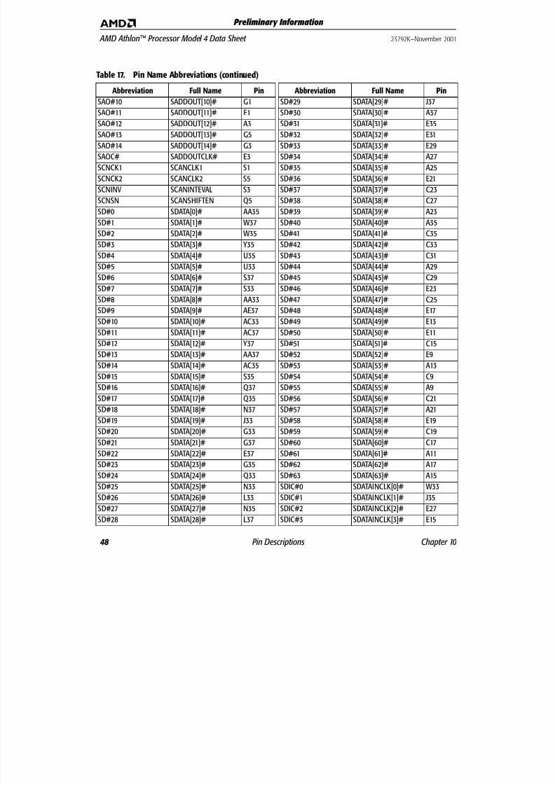
8/13/2019 Datasheet AMD Athlon II
http://slidepdf.com/reader/full/datasheet-amd-athlon-ii 62/88
48 Pin Descriptions Chapter 10
AMD Athlon™ Processor Model 4 Data Sheet 23792K—November 2001
Preliminary Information
SAO#10 SADDOUT[10]# G1
SAO#11 SADDOUT[11]# E1SAO#12 SADDOUT[12]# A3
SAO#13 SADDOUT[13]# G5
SAO#14 SADDOUT[14]# G3
SAOC# SADDOUTCLK# E3
SCNCK1 SCANCLK1 S1
SCNCK2 SCANCLK2 S5
SCNINV SCANINTEVAL S3
SCNSN SCANSHIFTEN Q5
SD#0 SDATA[0]# AA35
SD#1 SDATA[1]# W37SD#2 SDATA[2]# W35
SD#3 SDATA[3]# Y35
SD#4 SDATA[4]# U35
SD#5 SDATA[5]# U33
SD#6 SDATA[6]# S37
SD#7 SDATA[7]# S33
SD#8 SDATA[8]# AA33
SD#9 SDATA[9]# AE37
SD#10 SDATA[10]# AC33
SD#11 SDATA[11]# AC37SD#12 SDATA[12]# Y37
SD#13 SDATA[13]# AA37
SD#14 SDATA[14]# AC35
SD#15 SDATA[15]# S35
SD#16 SDATA[16]# Q37
SD#17 SDATA[17]# Q35
SD#18 SDATA[18]# N37
SD#19 SDATA[19]# J33
SD#20 SDATA[20]# G33
SD#21 SDATA[21]# G37
SD#22 SDATA[22]# E37
SD#23 SDATA[23]# G35
SD#24 SDATA[24]# Q33
SD#25 SDATA[25]# N33
SD#26 SDATA[26]# L33
SD#27 SDATA[27]# N35
SD#28 SDATA[28]# L37
Table 17. Pin Name Abbreviations (continued)
Abbreviation Full Name Pin
SD#29 SDATA[29]# J37
SD#30 SDATA[30]# A37SD#31 SDATA[31]# E35
SD#32 SDATA[32]# E31
SD#33 SDATA[33]# E29
SD#34 SDATA[34]# A27
SD#35 SDATA[35]# A25
SD#36 SDATA[36]# E21
SD#37 SDATA[37]# C23
SD#38 SDATA[38]# C27
SD#39 SDATA[39]# A23
SD#40 SDATA[40]# A35SD#41 SDATA[41]# C35
SD#42 SDATA[42]# C33
SD#43 SDATA[43]# C31
SD#44 SDATA[44]# A29
SD#45 SDATA[45]# C29
SD#46 SDATA[46]# E23
SD#47 SDATA[47]# C25
SD#48 SDATA[48]# E17
SD#49 SDATA[49]# E13
SD#50 SDATA[50]# E11SD#51 SDATA[51]# C15
SD#52 SDATA[52]# E9
SD#53 SDATA[53]# A13
SD#54 SDATA[54]# C9
SD#55 SDATA[55]# A9
SD#56 SDATA[56]# C21
SD#57 SDATA[57]# A21
SD#58 SDATA[58]# E19
SD#59 SDATA[59]# C19
SD#60 SDATA[60]# C17
SD#61 SDATA[61]# A11
SD#62 SDATA[62]# A17
SD#63 SDATA[63]# A15
SDIC#0 SDATAINCLK[0]# W33
SDIC#1 SDATAINCLK[1]# J35
SDIC#2 SDATAINCLK[2]# E27
SDIC#3 SDATAINCLK[3]# E15
Table 17. Pin Name Abbreviations (continued)
Abbreviation Full Name Pin

8/13/2019 Datasheet AMD Athlon II
http://slidepdf.com/reader/full/datasheet-amd-athlon-ii 63/88
Chapter 10 Pin Descriptions 49
23792K—November 2001 AMD Athlon™ Processor Model 4 Data Sheet
Preliminary Information
SDINV# SDATAINVALID# AN33
SDOC#0 SDATAOUTCLK[0]# AE35SDOC#1 SDATAOUTCLK[1]# C37
SDOC#2 SDATAOUTCLK[2]# A33
SDOC#3 SDATAOUTCLK[3]# C11
SDOV# SDATAOUTVALID# AL31
SFILLV# SFILLVALID# AJ31
SMI# AN5
STPC# STPCLK# AC1
SVRFM SYSVREFMODE AA5
TCK Q1
TDI U1TDO U5
TMS Q3
TRST# U3
VCC VCC_CORE B4
VCC VCC_CORE B8
VCC VCC_CORE B12
VCC VCC_CORE B16
VCC VCC_CORE B20
VCC VCC_CORE B24
VCC VCC_CORE B28 VCC VCC_CORE B32
VCC VCC_CORE B36
VCC VCC_CORE D2
VCC VCC_CORE D4
VCC VCC_CORE D8
VCC VCC_CORE D12
VCC VCC_CORE D16
VCC VCC_CORE D20
VCC VCC_CORE D24
VCC VCC_CORE D28
VCC VCC_CORE D32
VCC VCC_CORE F12
VCC VCC_CORE F16
VCC VCC_CORE F20
VCC VCC_CORE F24
VCC VCC_CORE F28
VCC VCC_CORE F32
Table 17. Pin Name Abbreviations (continued)
Abbreviation Full Name Pin
VCC VCC_CORE F34
VCC VCC_CORE F36 VCC VCC_CORE H2
VCC VCC_CORE H4
VCC VCC_CORE H12
VCC VCC_CORE H16
VCC VCC_CORE H20
VCC VCC_CORE H24
VCC VCC_CORE K32
VCC VCC_CORE K34
VCC VCC_CORE K36
VCC VCC_CORE M2 VCC VCC_CORE M4
VCC VCC_CORE M6
VCC VCC_CORE M8
VCC VCC_CORE P30
VCC VCC_CORE P32
VCC VCC_CORE P34
VCC VCC_CORE P36
VCC VCC_CORE R2
VCC VCC_CORE R4
VCC VCC_CORE R6 VCC VCC_CORE R8
VCC VCC_CORE T30
VCC VCC_CORE T32
VCC VCC_CORE T34
VCC VCC_CORE T36
VCC VCC_CORE V2
VCC VCC_CORE V4
VCC VCC_CORE V6
VCC VCC_CORE V8
VCC VCC_CORE X30
VCC VCC_CORE X32
VCC VCC_CORE X34
VCC VCC_CORE X36
VCC VCC_CORE Z2
VCC VCC_CORE Z4
VCC VCC_CORE Z6
VCC VCC_CORE Z8
Table 17. Pin Name Abbreviations (continued)
Abbreviation Full Name Pin

8/13/2019 Datasheet AMD Athlon II
http://slidepdf.com/reader/full/datasheet-amd-athlon-ii 64/88
50 Pin Descriptions Chapter 10
AMD Athlon™ Processor Model 4 Data Sheet 23792K—November 2001
Preliminary Information
VCC VCC_CORE AB30
VCC VCC_CORE AB32 VCC VCC_CORE AB34
VCC VCC_CORE AB36
VCC VCC_CORE AD2
VCC VCC_CORE AD4
VCC VCC_CORE AD6
VCC VCC_CORE AF14
VCC VCC_CORE AF18
VCC VCC_CORE AF22
VCC VCC_CORE AF26
VCC VCC_CORE AF34 VCC VCC_CORE AF36
VCC VCC_CORE AH2
VCC VCC_CORE AH4
VCC VCC_CORE AH10
VCC VCC_CORE AH14
VCC VCC_CORE AH18
VCC VCC_CORE AH22
VCC VCC_CORE AH26
VCC VCC_CORE AK10
VCC VCC_CORE AK14 VCC VCC_CORE AK18
VCC VCC_CORE AK22
VCC VCC_CORE AK26
VCC VCC_CORE AK30
VCC VCC_CORE AK34
VCC VCC_CORE AK36
VCC VCC_CORE AJ5
VCC VCC_CORE AL5
VCC VCC_CORE AM2
VCC VCC_CORE AM10
VCC VCC_CORE AM14
VCC VCC_CORE AM18
VCC VCC_CORE AM22
VCC VCC_CORE AM26
VCC VCC_CORE AM22
VCC VCC_CORE AM26
VCC VCC_CORE AM30
Table 17. Pin Name Abbreviations (continued)
Abbreviation Full Name Pin
VCC VCC_CORE AM34
VCCA AJ23 VCC_Z AC7
VID[0] L1
VID[1] L3
VID[2] L5
VID[3] L7
VID[4] J7
VREF_S VREF_SYS W5
VSS B2
VSS B6
VSS B10 VSS B14
VSS B18
VSS B22
VSS B26
VSS B30
VSS B34
VSS D6
VSS D10
VSS D14
VSS D18 VSS D22
VSS D26
VSS D30
VSS D34
VSS D36
VSS F2
VSS F4
VSS F6
VSS F10
VSS F14
VSS F18
VSS F22
VSS F26
VSS H14
VSS H18
VSS H22
VSS H26
Table 17. Pin Name Abbreviations (continued)
Abbreviation Full Name Pin

8/13/2019 Datasheet AMD Athlon II
http://slidepdf.com/reader/full/datasheet-amd-athlon-ii 65/88
Chapter 10 Pin Descriptions 51
23792K—November 2001 AMD Athlon™ Processor Model 4 Data Sheet
Preliminary Information
VSS H34
VSS H36 VSS K2
VSS K4
VSS K6
VSS M30
VSS M32
VSS M34
VSS M36
VSS P2
VSS P4
VSS P6 VSS P8
VSS R30
VSS R32
VSS R34
VSS R36
VSS T2
VSS T4
VSS T6
VSS T8
VSS V30 VSS V32
VSS V34
VSS V36
VSS X2
VSS X4
VSS X6
VSS X8
VSS Z30
VSS Z32
VSS Z34
VSS Z36
VSS AB2
VSS AB8
VSS AB4
VSS AB6
VSS AD32
VSS AD34
Table 17. Pin Name Abbreviations (continued)
Abbreviation Full Name Pin
VSS AD36
VSS AF2 VSS AF4
VSS AF12
VSS AF16
VSS AH12
VSS AH16
VSS AH20
VSS AH24
VSS AH28
VSS AH32
VSS AH34 VSS AH36
VSS AK2
VSS AK4
VSS AK12
VSS AK16
VSS AK20
VSS AK24
VSS AK28
VSS AK32
VSS AM4 VSS AM6
VSS AM12
VSS AM16
VSS AM20
VSS AM24
VSS AM28
VSS AM32
VSS AM36
VSS_Z AE7
ZN AC5
ZP AE5
Table 17. Pin Name Abbreviations (continued)
Abbreviation Full Name Pin
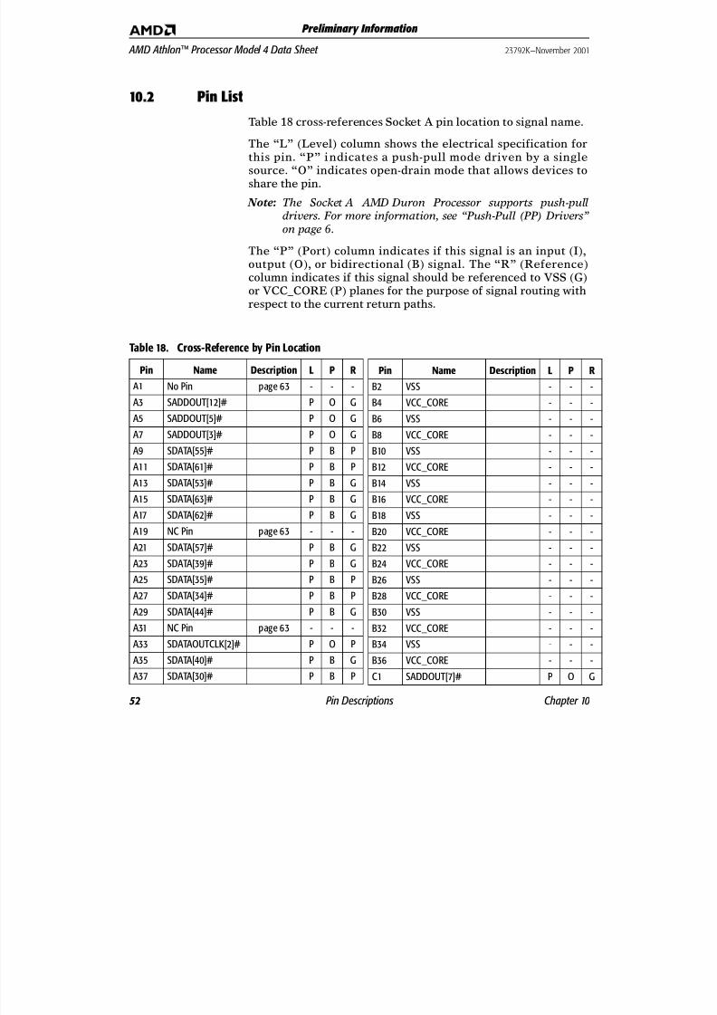
8/13/2019 Datasheet AMD Athlon II
http://slidepdf.com/reader/full/datasheet-amd-athlon-ii 66/88
52 Pin Descriptions Chapter 10
AMD Athlon™ Processor Model 4 Data Sheet 23792K—November 2001
Preliminary Information
Table 18. Cross-Reference by Pin Location
Pin Name Description L P R
A1 No Pin page 63 - - -
A3 SADDOUT[12]# P O G
A5 SADDOUT[5]# P O G
A7 SADDOUT[3]# P O G
A9 SDATA[55]# P B P
A11 SDATA[61]# P B P
A13 SDATA[53]# P B G
A15 SDATA[63]# P B G
A17 SDATA[62]# P B G
A19 NC Pin page 63 - - -
A21 SDATA[57]# P B G
A23 SDATA[39]# P B G
A25 SDATA[35]# P B P
A27 SDATA[34]# P B P
A29 SDATA[44]# P B G
A31 NC Pin page 63 - - -
A33 SDATAOUTCLK[2]# P O P
A35 SDATA[40]# P B G
A37 SDATA[30]# P B P
B2 VSS - - -
B4 VCC_CORE - - -
B6 VSS - - -
B8 VCC_CORE - - -
B10 VSS - - -
B12 VCC_CORE - - -
B14 VSS - - -
B16 VCC_CORE - - -
B18 VSS - - -
B20 VCC_CORE - - -
B22 VSS - - -
B24 VCC_CORE - - -
B26 VSS - - -
B28 VCC_CORE - - -
B30 VSS - - -
B32 VCC_CORE - - -
B34 VSS - - -
B36 VCC_CORE - - -
C1 SADDOUT[7]# P O G
Table 18. Cross-Reference by Pin Location
Pin Name Description L P R
10.2 Pin List
Table 18 cross-references Socket A pin location to signal name.
The “L” (Level) column shows the electrical specification forthis pin. “P” indicates a push-pull mode driven by a singlesource. “O” indicates open-drain mode that allows devices toshare the pin.
Note: The Socket A AMD Duron Processor supports push-pulldrivers. For more information, see “Push-Pull (PP) Drivers”
on page 6.
The “P” (Port) column indicates if this signal is an input (I),output (O), or bidirectional (B) signal. The “R” (Reference)column indicates if this signal should be referenced to VSS (G)
or VCC_CORE (P) planes for the purpose of signal routing withrespect to the current return paths.

8/13/2019 Datasheet AMD Athlon II
http://slidepdf.com/reader/full/datasheet-amd-athlon-ii 67/88
Chapter 10 Pin Descriptions 53
23792K—November 2001 AMD Athlon™ Processor Model 4 Data Sheet
Preliminary Information
C3 SADDOUT[9]# P O G
C5 SADDOUT[8]# P O G
C7 SADDOUT[2]# P O G
C9 SDATA[54]# P B P
C11 SDATAOUTCLK[3]# P O G
C13 NC Pin page 63 - - -
C15 SDATA[51]# P B P
C17 SDATA[60]# P B G
C19 SDATA[59]# P B G
C21 SDATA[56]# P B G
C23 SDATA[37]# P B P
C25 SDATA[47]# P B G
C27 SDATA[38]# P B G
C29 SDATA[45]# P B G
C31 SDATA[43]# P B G
C33 SDATA[42]# P B G
C35 SDATA[41]# P B G
C37 SDATAOUTCLK[1]# P O G
D2 VCC_CORE - - -
D4 VCC_CORE - - -
D6 VSS - - -
D8 VCC_CORE - - -
D10 VSS - - -
D12 VCC_CORE - - -
D14 VSS - - -
D16 VCC_CORE - - -
D18 VSS - - -
D20 VCC_CORE - - -
D22 VSS - - -
D24 VCC_CORE - - -
D26 VSS - - -
D28 VCC_CORE - - -
D30 VSS - - -
D32 VCC_CORE - - -
Table 18. Cross-Reference by Pin Location
Pin Name Description L P R
D34 VSS - - -
D36 VSS - - -
E1 SADDOUT[11]# P O P
E3 SADDOUTCLK# P O G
E5 SADDOUT[4]# P O P
E7 SADDOUT[6]# P O G
E9 SDATA[52]# P B P
E11 SDATA[50]# P B P
E13 SDATA[49]# P B G
E15 SDATAINCLK[3]# P I G
E17 SDATA[48]# P B P
E19 SDATA[58]# P B G
E21 SDATA[36]# P B P
E23 SDATA[46]# P B P
E25 NC Pin page 63 - - -
E27 SDATAINCLK[2]# P I G
E29 SDATA[33]# P B P
E31 SDATA[32]# P B P
E33 NC Pin page 63 - - -
E35 SDATA[31]# P B P
E37 SDATA[22]# P B G
F2 VSS - - -
F4 VSS - - -
F6 VSS - - -
F8 NC Pin page 63 - - -
F10 VSS - - -
F12 VCC_CORE - - -
F14 VSS - - -
F16 VCC_CORE - - -
F18 VSS - - -
F20 VCC_CORE - - -
F22 VSS - - -
F24 VCC_CORE - - -
F26 VSS - - -
Table 18. Cross-Reference by Pin Location
Pin Name Description L P R
(continued)

8/13/2019 Datasheet AMD Athlon II
http://slidepdf.com/reader/full/datasheet-amd-athlon-ii 68/88
54 Pin Descriptions Chapter 10
AMD Athlon™ Processor Model 4 Data Sheet 23792K—November 2001
Preliminary Information
F28 VCC_CORE - - -
F30 NC Pin page 63 - - -
F32 VCC_CORE - - -
F34 VCC_CORE - - -
F36 VCC_CORE - - -
G1 SADDOUT[10]# P O P
G3 SADDOUT[14]# P O G
G5 SADDOUT[13]# P O G
G7 Key Pin page 63 - - -
G9 Key Pin page 63 - - -
G11 NC Pin page 63 - - -
G13 NC Pin page 63 - - -
G15 Key Pin page 63 - - -
G17 Key Pin page 63 - - -
G19 NC Pin page 63 - - -
G21 NC Pin page 63 - - -
G23 Key Pin page 63 - - -
G25 Key Pin page 63 - - -
G27 NC Pin page 63 - - -
G29 NC Pin page 63 - - -
G31 NC Pin page 63 - - -
G33 SDATA[20]# P B G
G35 SDATA[23]# P B G
G37 SDATA[21]# P B G
H2 VCC_CORE - - -
H4 VCC_CORE - - -
H6 NC Pin page 63 - - -
H8 NC Pin page 63 - - -
H10 NC Pin page 63 - - -
H12 VCC_CORE - - -
H14 VSS - - -
H16 VCC_CORE - - -
H18 VSS - - -
H20 VCC_CORE - - -
Table 18. Cross-Reference by Pin Location
Pin Name Description L P R
H22 VSS - - -
H24 VCC_CORE - - -
H26 VSS - - -
H28 NC Pin page 63 - - -
H30 NC Pin page 63 - - -
H32 NC Pin page 63 - - -
H34 VSS - - -
H36 VSS - - -
J1 SADDOUT[0]# page 64 P O -
J3 SADDOUT[1]# page 64 P O -
J5 NC Pin page 63 - - -
J7 VID[4] page 65 O O -
J31 NC Pin page 63 - - -
J33 SDATA[19]# P B G
J35 SDATAINCLK[1]# P I P
J37 SDATA[29]# P B P
K2 VSS - - -
K4 VSS - - -
K6 VSS - - -
K8 NC Pin page 63 - - -
K30 NC Pin page 63 - - -
K32 VCC_CORE - - -
K34 VCC_CORE - - -
K36 VCC_CORE - - -
L1 VID[0] page 65 O O -
L3 VID[1] page 65 O O -
L5 VID[2] page 65 O O -
L7 VID[3] page 65 O O -
L31 NC Pin page 63 - - -
L33 SDATA[26]# P B P
L35 NC Pin page 63 - - -
L37 SDATA[28]# P B P
M2 VCC_CORE - - -
M4 VCC_CORE - - -
Table 18. Cross-Reference by Pin Location
Pin Name Description L P R
(continued)

8/13/2019 Datasheet AMD Athlon II
http://slidepdf.com/reader/full/datasheet-amd-athlon-ii 69/88
Chapter 10 Pin Descriptions 55
23792K—November 2001 AMD Athlon™ Processor Model 4 Data Sheet
Preliminary Information
M6 VCC_CORE - - -
M8 VCC_CORE - - -
M30 VSS - - -
M32 VSS - - -
M34 VSS - - -
M36 VSS - - -
N1 PICCLK page 60 O I -
N3 PICD#[0] page 60 O B -
N5 PICD#[1] page 60 O B -
N7 Key Pin page 63 - - -
N31 NC Pin page 63 - - -
N33 SDATA[25]# P B P
N35 SDATA[27]# P B P
N37 SDATA[18]# P B G
P2 VSS - - -
P4 VSS - - -
P6 VSS - - -
P8 VSS - - -
P30 VCC_CORE - - -
P32 VCC_CORE - - -
P34 VCC_CORE - - -
P36 VCC_CORE - - -
Q1 TCK page 63 P I -
Q3 TMS page 63 P I -
Q5 SCANSHIFTEN page 64 P I -
Q7 Key Pin page 63 - - -
Q31 NC Pin page 63 - - -
Q33 SDATA[24]# P B P
Q35 SDATA[17]# P B G
Q37 SDATA[16]# P B G
R2 VCC_CORE - - -
R4 VCC_CORE - - -
R6 VCC_CORE - - -
R8 VCC_CORE - - -
Table 18. Cross-Reference by Pin Location
Pin Name Description L P R
R30 VSS - - -
R32 VSS - - -
R34 VSS - - -
R36 VSS - - -
S1 SCANCLK1 page 64 P I -
S3 SCANINTEVAL page 64 P I -
S5 SCANCLK2 page 64 P I -
S7 NC Pin page 63 - - -
S31 NC Pin page 63 - - -
S33 SDATA[7]# P B G
S35 SDATA[15]# P B P
S37 SDATA[6]# P B G
T2 VSS - - -
T4 VSS - - -
T6 VSS - - -
T8 VSS - - -
T30 VCC_CORE - - -
T32 VCC_CORE - - -
T34 VCC_CORE - - -
T36 VCC_CORE - - -
U1 TDI page 63 P I -
U3 TRST# page 63 P I -
U5 TDO page 63 P O -
U7 NC Pin page 63 - - -
U31 NC Pin page 63 - - -
U33 SDATA[5]# P B G
U35 SDATA[4]# P B G
U37 NC Pin page 63 - - -
V2 VCC_CORE - - -
V4 VCC_CORE - - -
V6 VCC_CORE - - -
V8 VCC_CORE - - -
V30 VSS - - -
V32 VSS - - -
Table 18. Cross-Reference by Pin Location
Pin Name Description L P R
(continued)

8/13/2019 Datasheet AMD Athlon II
http://slidepdf.com/reader/full/datasheet-amd-athlon-ii 70/88
56 Pin Descriptions Chapter 10
AMD Athlon™ Processor Model 4 Data Sheet 23792K—November 2001
Preliminary Information
V34 VSS - - -
V36 VSS - - -
W1 FID[0] page 62 O - -
W3 FID[1] page 62 O - -
W5 VREFSYS page 66 P - -
W7 NC Pin page 63 - - -
W31 NC Pin page 63 - - -
W33 SDATAINCLK[0]# P I G
W35 SDATA[2]# P B G
W37 SDATA[1]# P B P
X2 VSS - - -
X4 VSS - - -
X6 VSS - - -
X8 VSS - - -
X30 VCC_CORE - - -
X32 VCC_CORE - - -
X34 VCC_CORE - - -
X36 VCC_CORE - - -
Y1 FID[2] page 62 O - -
Y3 FID[3] page 62 O - -
Y5 NC Pin page 63 - - -
Y7 Key Pin page 63 - - -
Y31 NC Pin page 63 - - -
Y33 NC Pin page 63 - - -
Y35 SDATA[3]# P B G
Y37 SDATA[12]# P B P
Z2 VCC_CORE - - -
Z4 VCC_CORE - - -
Z6 VCC_CORE - - -
Z8 VCC_CORE - - -
Z30 VSS - - -
Z32 VSS - - -
Z34 VSS - - -
Z36 VSS - - -
Table 18. Cross-Reference by Pin Location
Pin Name Description L P R
AA1 DBRDY page 61 P O -
AA3 DBREQ# page 61 P I -
AA5 SYSVREFMODE page 64 P I -
AA7 Key Pin page 63 - - -
AA31 NC Pin page 63 - - -
AA33 SDATA[8]# P B P
AA35 SDATA[0]# P B G
AA37 SDATA[13]# P B G
AB2 VSS - - -
AB4 VSS - - -
AB6 VSS - - -
AB8 VSS - - -
AB30 VCC_CORE - - -
AB32 VCC_CORE - - -
AB34 VCC_CORE - - -
AB36 VCC_CORE - - -
AC1 STPCLK# page 64 P I -
AC3 PLLTEST# page 64 P I -
AC5 ZN page 66 P - -
AC7 VCC_Z page 66 - - -
AC31 NC Pin page 63 - - -
AC33 SDATA[10]# P B P
AC35 SDATA[14]# P B G
AC37 SDATA[11]# P B G
AD2 VCC_CORE - - -
AD4 VCC_CORE - - -
AD6 VCC_CORE - - -
AD8 NC Pin page 63 - - -
AD30 NC Pin page 63 - - -
AD32 VSS - - -
AD34 VSS - - -
AD36 VSS - - -
AE1 A20M# P I -
AE3 PWROK P I -
Table 18. Cross-Reference by Pin Location
Pin Name Description L P R
(continued)

8/13/2019 Datasheet AMD Athlon II
http://slidepdf.com/reader/full/datasheet-amd-athlon-ii 71/88
Chapter 10 Pin Descriptions 57
23792K—November 2001 AMD Athlon™ Processor Model 4 Data Sheet
Preliminary Information
AE5 ZP page 66 P - -
AE7 VSS_Z page 66 - - -
AE31 NC Pin page 63 - - -
AE33 SADDIN[5]# P I G
AE35 SDATAOUTCLK[0]# P O P
AE37 SDATA[9]# P B G
AF2 VSS - - -
AF4 VSS - - -
AF6 NC Pin page 63 - - -
AF8 NC Pin page 63 - - -
AF10 NC Pin page 63 - - -
AF12 VSS - - -
AF14 VCC_CORE - - -
AF16 VSS - - -
AF18 VCC_CORE - - -
AF20 VSS - - -
AF22 VCC_CORE - - -
AF24 VSS - - -
AF26 VCC_CORE - - -
AF28 NC Pin page 63 - - -
AF30 NC Pin page 63 - - -
AF32 NC Pin page 63 - - -
AF34 VCC_CORE - - -
AF36 VCC_CORE - - -
AG1 FERR page 61 P O -
AG3 RESET# - I -
AG5 NC Pin page 63 - - -
AG7 Key Pin page 63 - - -
AG9 Key Pin page 63 - - -
AG11 COREFB page 61 - - -
AG13 COREFB# page 61 - - -
AG15 Key Pin page 63 - - -
AG17 Key Pin page 63 - - -
AG19 NC Pin page 63 - - -
Table 18. Cross-Reference by Pin Location
Pin Name Description L P R
AG21 NC Pin page 63 - - -
AG23 NC Pin page 63 - - -
AG25 NC Pin page 63 - - -
AG27 Key Pin page 63 - - -
AG29 Key Pin page 63 - - -
AG31 NC Pin page 63 - - -
AG33 SADDIN[2]# P I G
AG35 SADDIN[11]# P I G
AG37 SADDIN[7]# P I P
AH2 VCC_CORE - - -
AH4 VCC_CORE - - -
AH6 AMD Pin page 60 - - -
AH8 NC Pin page 63 - - -
AH10 VCC_CORE - - -
AH12 VSS - - -
AH14 VCC_CORE - - -
AH16 VSS - - -
AH18 VCC_CORE - - -
AH20 VSS - - -
AH22 VCC_CORE - - -
AH24 VSS - - -
AH26 VCC_CORE - - -
AH28 VSS - - -
AH30 NC Pin page 63 - - -
AH32 VSS - - -
AH34 VSS - - -
AH36 VSS - - -
AJ1 IGNNE# page 63 P I -
AJ3 INIT# page 63 P I -
AJ5 VCC_CORE - - -
AJ7 NC Pin page 63 - - -
AJ9 NC Pin page 63 - - -
AJ11 NC Pin page 63 - - -
AJ13 Analog page 60 - - -
Table 18. Cross-Reference by Pin Location
Pin Name Description L P R
(continued)

8/13/2019 Datasheet AMD Athlon II
http://slidepdf.com/reader/full/datasheet-amd-athlon-ii 72/88
58 Pin Descriptions Chapter 10
AMD Athlon™ Processor Model 4 Data Sheet 23792K—November 2001
Preliminary Information
AJ15 NC Pin page 63 - - -
AJ17 NC Pin page 63 - - -
AJ19 NC Pin page 63 - - -
AJ21 CLKFWDRST page 60 P I P
AJ23 VCCA page 65 - - -
AJ25 PLLBYPASS# page 64 P I -
AJ27 NC Pin page 63 - - -
AJ29 SADDIN[0]# page 64 P I -
AJ31 SFILLVALID# P I G
AJ33 SADDINCLK# P I G
AJ35 SADDIN[6]# P I P
AJ37 SADDIN[3]# P I G
AK2 VSS - - -
AK4 VSS - - -
AK6 CPU_PRESENCE# page 61 - - -
AK8 NC Pin page 63 - - -
AK10 VCC_CORE - - -
AK12 VSS - - -
AK14 VCC_CORE - - -
AK16 VSS - - -
AK18 VCC_CORE - - -
AK20 VSS - - -
AK22 VCC_CORE - - -
AK24 VSS - - -
AK26 VCC_CORE - - -
AK28 VSS - - -
AK30 VCC_CORE - - -
AK32 VSS - - -
AK34 VCC_CORE - - -
AK36 VCC_CORE - - -
AL1 INTR page 63 P I -
AL3 FLUSH# page 63 P I -
AL5 VCC_CORE - - -
AL7 NC Pin page 63 - - -
Table 18. Cross-Reference by Pin Location
Pin Name Description L P R
AL9 NC Pin page 63 - - -
AL11 NC Pin page 63 - - -
AL13 PLLMON2 page 64 O O -
AL15 PLLBYPASSCLK# page 64 P I -
AL17 CLKIN# page 60 P I P
AL19 RSTCLK# page 60 P I P
AL21 K7CLKOUT page 63 P O -
AL23 CONNECT page 60 P I P
AL25 NC Pin page 63 - - -
AL27 NC Pin page 63 - - -
AL29 SADDIN[1]# page 64 P I -
AL31 SDATAOUTVALID# P O P
AL33 SADDIN[8]# P I P
AL35 SADDIN[4]# P I G
AL37 SADDIN[10]# P I G
AM2 VCC_CORE - - -
AM4 VSS - - -
AM6 VSS - - -
AM8 NC Pin page 63 - - -
AM10 VCC_CORE - - -
AM12 VSS - - -
AM14 VCC_CORE - - -
AM16 VSS - - -
AM18 VCC_CORE - - -
AM20 VSS - - -
AM22 VCC_CORE - - -
AM24 VSS - - -
AM26 VCC_CORE - - -
AM28 VSS - - -
AM30 VCC_CORE - - -
AM32 VSS - - -
AM34 VCC_CORE - - -
AM36 VSS - - -
AN1 No Pin page 63 - - -
Table 18. Cross-Reference by Pin Location
Pin Name Description L P R
(continued)

8/13/2019 Datasheet AMD Athlon II
http://slidepdf.com/reader/full/datasheet-amd-athlon-ii 73/88
Chapter 10 Pin Descriptions 59
23792K—November 2001 AMD Athlon™ Processor Model 4 Data Sheet
Preliminary Information
AN3 NMI P I -
AN5 SMI# P I -
AN7 NC Pin page 63 - - -
AN9 NC Pin page 63 - - -
AN11 NC Pin page 63 - - -
AN13 PLLMON1 page 64 O B -
AN15 PLLBYPASSCLK page 64 P I -
AN17 CLKIN page 60 P I P
AN19 RSTCLK page 60 P I P
AN21 K7CLKOUT# page 63 P O -
AN23 PROCRDY P O P
AN25 NC Pin page 63 - - -
AN27 NC Pin page 63 - - -
AN29 SADDIN[12]# P I G
AN31 SADDIN[14]# P I G
AN33 SDATAINVALID# P I P
AN35 SADDIN[13]# P I G
AN37 SADDIN[9]# P I G
Table 18. Cross-Reference by Pin Location
Pin Name Description L P R
(continued)

8/13/2019 Datasheet AMD Athlon II
http://slidepdf.com/reader/full/datasheet-amd-athlon-ii 74/88
60 Pin Descriptions Chapter 10
AMD Athlon™ Processor Model 4 Data Sheet 23792K—November 2001
Preliminary Information
10.3 Detailed Pin Descriptions
The information in this section pertains to Table 18 on page 52.
A20M# Pin A20M# is an input from the system used to simulate addresswrap-around in the 20-bit 8086.
AMD Pin AMD Socket A processors do not implement a pin at location
AH6. All Socket A designs must have a top plate or cover thatblocks this pin location. When the cover plate blocks this
location, a non-AMD part (e.g., PGA370) does not fit into the
socket. However, socket manufacturers are allowed to have acontact loaded in the AH6 position. Therefore, motherboard
socket design should account for the possibility that a contact
could be loaded in this position.
AMD Athlon™System Bus Pins
See the AMD Athlon™ and AMD Duron™ System Bus
Specification, order# 21902 for information about the systembus pins —PROCRDY, PWROK, RESET#, SADDIN[14:2]#,SADDINCLK#, SADDOUT[14:2]#, SADDOUTCLK#,
SDATA[63: 0]#, SDATAINCLK[3:0 ]#, SDATAINVALID#,SDATAOUTCLK[3:0]#, SDATAOUTVALID#, SFILLVALID#.
Analog Pin Treat this pin as a NC.
APIC Pins, PICCLK,
PICD[1:0]#
The Advanced Programmable Interrupt Controller (APIC) is a
feature that provides a flexible and expandable means ofdelivering interrupts in a system using an AMD processor. The
pins, PICD[1:0], are the bi-directional message-passing signals
used for the APIC and are driven to the Southbridge or adedicated I/O APIC. The pin, PICCLK, must be driven with a
valid clock input. For more information, see Table 14, “APIC
Pins AC and DC Characteristics,” on page 34.
CLKFWDRST Pin CLKFWDRST resets clock-forward circuitry for both the systemand processor.
CLKIN, RSTCLK(SYSCLK) Pins Connect CLKIN (AN17) with RSTCLK (AN19) and name itSYSCLK. Connect CLKIN# (AL17) with RSTCLK# (AL19) and
name it SYSCLK#. Length match the clocks from the clock
generator to the Northbridge and processor. See “SYSCLK andSYSCLK# Pins” on page 64 for more information.
CONNECT Pin CONNECT is an input from the system used for powermanagement and clock-forward initialization at reset.

8/13/2019 Datasheet AMD Athlon II
http://slidepdf.com/reader/full/datasheet-amd-athlon-ii 75/88
Chapter 10 Pin Descriptions 61
23792K—November 2001 AMD Athlon™ Processor Model 4 Data Sheet
Preliminary Information
COREFB andCOREFB# Pins
COREFB and COREFB# are outputs to the system that provideprocessor core voltage feedback to the system.
CPU_PRESENCE# Pin CPU_PRESENCE# is connected to VSS on the processor
package. If pulled-up on the motherboard, CPU_PRESENCE#can be used to detect the presence or absence of a processor inthe Socket A–style socket.
DBRDY and DBREQ#Pins
DBRDY (AA1) and DBREQ# (AA3) are routed to the debugconnector. DBREQ# is tied to VCC_CORE with a pullup
resistor.
FERR Pin FERR is an output to the system that is asserted for anyunmasked numerical exception independent of the NE bit in
CR0. FERR is a push-pull active High signal that must be
inverted and level shifted to an active Low signal. For moreinformation about FERR and FERR#, see the “Required
Circuits” chapter of the AMD Athlon™ Processor-Based Motherboard Design Guide order# 24363.
FID[3:0] Pins See “Frequency Identification (FID[3:0])” on page 24 for theAC and DC characteristics for FID[3:0].
FID[3] (Y3), FID[2] (Y1), FID[1] (W3), and FID[0] (W1) are the4-bit processor clock-to-SYSCLK ratio. Table 19 on page 62
describes the encodings of the clock multipliers on FID[3:0].

8/13/2019 Datasheet AMD Athlon II
http://slidepdf.com/reader/full/datasheet-amd-athlon-ii 76/88
62 Pin Descriptions Chapter 10
AMD Athlon™ Processor Model 4 Data Sheet 23792K—November 2001
Preliminary Information
The FID[3:0] signals are open drain processor outputs that arepulled High on the motherboard and sampled by the chipset atthe deassertion of RESET# to determine the SIP (Serialization
Initialization Packet) that gets sent to the processor. See the AMD Athlon™ and AMD Duron™ System Bus Specification,order#21902 for more information about the Serialization
Initialization Packets and SIP protocol.
The processor FID[3:0] outputs are open drain and 2.5Vtolerant. To prevent damage to the processor, if these signalsare pulled High to above 2.5 V, they must be electrical ly
isolated from the processor. For information about the FID[3:0]isolation circuit, see the AMD Athlon™ Processor-Based
Motherboard Design Guide , order# 24363.
Table 19. FID[3:0] Clock Multiplier Encodings
FID[3] FID[2] FID[1] FID[0] Processor Clock toSYSCLK FrequencyRatio
0 0 0 0 11
0 0 0 1 11.5
0 0 1 0 12
0 0 1 1 ≥ 12.5*
0 1 0 0 5
0 1 0 1 5.5
0 1 1 0 6
0 1 1 1 6.5
1 0 0 0 7
1 0 0 1 7.5
1 0 1 0 8
1 0 1 1 8.5
1 1 0 0 9
1 1 0 1 9.5
1 1 1 0 10
1 1 1 1 10.5
Note:
*All ratios greater than or equal to 12.5x have the same FID[3:0] code of 0011, which causesthe SIP configuration for all ratios of 12.5x or greater to be the same.

8/13/2019 Datasheet AMD Athlon II
http://slidepdf.com/reader/full/datasheet-amd-athlon-ii 77/88
Chapter 10 Pin Descriptions 63
23792K—November 2001 AMD Athlon™ Processor Model 4 Data Sheet
Preliminary Information
FLUSH# Pin FLUSH# must be tied to VCC_CORE with a pullup resistor. If adebug connector is implemented, FLUSH# is routed to the
debug connector.
IGNNE# Pin IGNNE# is an input from the system that tells the processor toignore numeric errors.
INIT# Pin INIT# is an input from the system that resets the integer
registers without affecting the floating-point registers or theinternal caches. Execution starts at 0_FFFF_FFF0h.
INTR Pin INTR is an input from the system that causes the processor tostart an interrupt acknowledge transaction that fetches the8-bit interrupt vector and starts execution at that location.
JTAG Pins TCK (Q1), TMS (Q3), TDI (U1), TRST# (U3), and TDO (U5) arethe JTAG interface. Connect these pins directly to themotherboard debug connector. Pullup TDI, TCK, TMS, andTRST# to VCC_CORE with pullup resistors.
K7CLKOUT andK7CLKOUT# Pins
K7CLKOUT (AL21) and K7CLKOUT# (AN21) are each run for 2to 3 inches and then terminated with a resistor pair, 100 ohms to
VCC_CORE and 100 ohms to VSS. The effective terminationresistance and voltage are 50 ohms and VCC_CORE/2.
Key Pins These 16 locations are for processor type keying for forwards
and backwards compatibility (G7, G9, G15, G17, G23, G25, N7,Q7, Y7, AA7, AG7, AG9, AG15, AG17, AG27, and AG29).Motherboard designers should treat key pins like NC (noconnect) pins. See “NC Pins” on page 63 for more information.
A socket designer has the option of creating a top mold piecethat allows PGA key pins only where designated. However,sockets that populate all 16 key pins must be allowed, so the
motherboard must always provide for pins at all key pinlocations.
NC Pins The motherboard should provide a plated hole for an NC pin.
The pin hole should not be electrically connected to anything.
NMI Pin NMI is an input from the system that causes a non-maskable
interrupt.
PGA Orientation Pins No pin is present at pin locations A1 and AN1. Motherboarddesigners should not allow for a PGA socket pin at theselocations.

8/13/2019 Datasheet AMD Athlon II
http://slidepdf.com/reader/full/datasheet-amd-athlon-ii 78/88
64 Pin Descriptions Chapter 10
AMD Athlon™ Processor Model 4 Data Sheet 23792K—November 2001
Preliminary Information
For more information, see the AMD Athlon™ Processor-Based Motherboard Design Guide , order# 24363.
PLL Bypass and Test
Pins
PLLTEST# (AC3), PLLBYPASS# (AJ25), PLLMON1 (AN13),
PLLMON2 (AL13) , PLLBYPASSCLK (AN15), andPLLBYPASSCLK# (AL15) are the PLL bypass and testinterface. This interface is tied disabled on the motherboard.
All six pin signals are routed to the debug connector. All fourprocessor inputs (PLLTEST#, PLLBYPASS#, PLLMON1, andPLLMON2) are tied to VCC_CORE with pullup resistors.
PWROK Pin The PWROK input to the processor must not be asserted untilall voltage planes in the system are within specification and all
system clocks are running within specification.
For more information, See “Signal and Power-UpRequirements” on page 35.
SADDIN[1:0]# andSADDOUT[1:0]# Pins
The AMD Athlon processor model 4 does not support
SADDIN[1:0]# or SADDOUT[1:0]#. SADDIN[1]# is tied to VCCwith pullup resistors, if this bit is not supported by the
Northbridge (future models can support SADDIN[1]#).
SADDOUT[1:0]# are tied to VCC with pullup resistors if thesepins are supported by the Northbridge. For more information,
see the AMD Athlon™ and AMD Duron™ System Bus
Specification, order# 21902.
Scan Pins SCANSHIFTEN (Q5), SCANCLK1 (S1), SCANINTEVAL (S3),
and SCANCLK2 (S5) are the scan interface. This interface isAMD internal and is tied disabled with pulldown resistors toground on the motherboard.
SMI# Pin SMI# is an input that causes the processor to enter the system
management mode.
STPCLK# Pin STPCLK# is an input that causes the processor to enter a lower
power mode and issue a Stop Grant special cycle.
SYSCLK and SYSCLK#Pins
SYSCLK and SYSCLK# are differential input clock signalsprovided to the processor’s PLL from a system-clock generator.
See “CLKIN, RSTCLK (SYSCLK) Pins” on page 60 for moreinformation.
SYSVREFMODE Pin SYSVREFMODE (AA5) is Low to ensure that the external
VREFSYS voltage is the actual voltage used by the input
buffers and that no scaling occurs internally between the

8/13/2019 Datasheet AMD Athlon II
http://slidepdf.com/reader/full/datasheet-amd-athlon-ii 79/88
Chapter 10 Pin Descriptions 65
23792K—November 2001 AMD Athlon™ Processor Model 4 Data Sheet
Preliminary Information
VREFSYS voltage and the input threshold. This pin is tied Lowwith a pulldown resistor.
VCCA Pin VCCA is the processor PLL supply. For information about the
VCCA pin, see Table 5, “VCCA AC and DC Characteristics,” onpage 25 and the AMD Athlon™ Processor-Based Motherboard
Design Guide , order# 24363.
VID[4:0] Pins The VID[4:0] (Voltage Identification) outputs are used todictate the VCC_CORE voltage level. The VID[4:0] pins are
strapped to ground or left unconnected on the processor’s
package. The VID[4:0] pins are pulled-up on the motherboardand used by the VCC_CORE DC/DC converter.
These voltage ID values are defined Table 20 on page 66.

8/13/2019 Datasheet AMD Athlon II
http://slidepdf.com/reader/full/datasheet-amd-athlon-ii 80/88
66 Pin Descriptions Chapter 10
AMD Athlon™ Processor Model 4 Data Sheet 23792K—November 2001
Preliminary Information
For more information, see the “Required Circuits” chapter ofthe AMD Athlon™ Processor-Based Motherboard Design Guide ,order# 24363.
VREFSYS Pin VREFSYS (W5) drives the threshold voltage for the system businput receivers. The value of VREFSYS is system specific. In
addition, to minimize VCC_CORE noise rejection fromVREFSYS, include decoupling capacitors. For moreinformation, see the AMD Athlon™ Processor-Based Motherboard
Design Guide , order# 24363.
ZN, VCC_Z, ZP, andVSS_Z Pins
ZN (AC5), VCC_Z (AC7), ZP (AE5), and VSS_Z(AE7) are thepush-pull compensation circuit pins. VCC_Z is tied toVCC_CORE. VSS_Z is tied to VSS.
In Push-Pull mode (selected by the SIP parameter SysPushPullasserted), ZN is tied to VCC_CORE with a resistor that has a
resistance matching the impedance Z0 of the transmission line.ZP is tied to VSS with a resistor that has a resistance matchingthe impedance Z0 of the transmission line.
Table 20. VID[4:0] Code to Voltage Definition
VID[4:0] VCC_CORE (V) VID[4:0] VCC_CORE (V)
00000 1.850 10000 1.450
00001 1.825 10001 1.425
00010 1.800 10010 1.400
00011 1.775 10011 1.375
00100 1.750 10100 1.350
00101 1.725 10101 1.325
00110 1.700 10110 1.300
00111 1.675 10111 1.275
01000 1.650 11000 1.250
01001 1.625 11001 1.225
01010 1.600 11010 1.200
01011 1.575 11011 1.175
01100 1.550 11100 1.150
01101 1.525 11101 1.125
01110 1.500 11110 1.100
01111 1.475 11111 No CPU
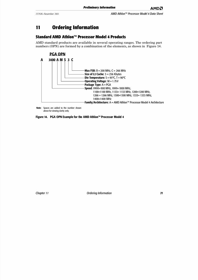
8/13/2019 Datasheet AMD Athlon II
http://slidepdf.com/reader/full/datasheet-amd-athlon-ii 81/88
Chapter 11 Ordering Information 71
23792K—November 2001 AMD Athlon™ Processor Model 4 Data Sheet
Preliminary Information
11 Ordering Information
Standard AMD Athlon™ Processor Model 4 Products
AMD standard products are available in several operating ranges. The ordering partnumbers (OPN) are formed by a combination of the elements, as shown in Figure 14.
Figure 14. PGA OPN Example for the AMD Athlon™ Processor Model 4
A 1400 A M S 3 C
Note: Spaces are added to the number shownabove for viewing clarity only.
PGA OPN
Max FSB: B = 200 MHz, C = 266 MHzSize of L2 Cache: 3 = 256 KbytesDie Temperature: S = 95ºC, T = 90ºCOperating Voltage: M = 1.75V Package Type: A = PGASpeed: 0900= 900 MHz, 1000= 1000 MHz,
1100=1100 MHz, 1133= 1133 MHz, 1200=1200 MHz,1266 = 1266 MHz, 1300=1300 MHz, 1333= 1333 MHz,1400=1400 MHz
Family/Architecture: A = AMD Athlon™ Processor Model 4 Architecture

8/13/2019 Datasheet AMD Athlon II
http://slidepdf.com/reader/full/datasheet-amd-athlon-ii 82/88
72 Ordering Information Chapter 11
AMD Athlon™ Processor Model 4 Data Sheet 23792K—November 2001
Preliminary Information

8/13/2019 Datasheet AMD Athlon II
http://slidepdf.com/reader/full/datasheet-amd-athlon-ii 83/88

8/13/2019 Datasheet AMD Athlon II
http://slidepdf.com/reader/full/datasheet-amd-athlon-ii 84/88
74 Appendix A
AMD Athlon™ Processor Model 4 Data Sheet 23792K—November 2001
Preliminary Information
■ Invalid and Don’t-Care—In timing diagrams, signal rangesthat are invalid or don't-care are filled with a screen pattern.
Data TerminologyThe following list defines data terminology:
■ Quantities
ï A word is two bytes (16 bits)
ï A doubleword is four bytes (32 bits)
ï A quadword is eight bytes (64 bits)
■ Addressing—Memory is addressed as a series of bytes oneight-byte (64-bit) boundaries in which each byte can be
separately enabled.
■ Abbreviations—The following notation is used for bits andbytes:
ï Kilo (K, as in 4-Kbyte page)
ï Mega (M, as in 4 Mbits/sec)
ï Giga (G, as in 4 Gbytes of memory space)
See Table 21 on page 75 for more abbreviations.
■ Little-Endian Convention—The byte with the addressxx...xx00 is in the least-significant byte position (little end).In byte diagrams, bit positions are numbered from right to
left—the little end is on the right and the big end is on theleft. Data structure diagrams in memory show low addressesat the bottom and high addresses at the top. When data
items are aligned, bit notation on a 64-bit data bus mapsdirectly to bit notation in 64-bit-wide memory. Because byteaddresses increase from right to left, strings appear in
reverse order when illustrated.
■ Bit Ranges—In text, bit ranges are shown with a dash (forexample, bits 9–1). When accompanied by a signal or bus
name, the highest and lowest bit numbers are contained in
brackets and separated by a colon (for example, AD[31:0]).■ Bit Values—Bits can either be set to 1 or cleared to 0.
■ Hexadecimal and Binary Numbers—Unless the contextmakes interpretation clear, hexadecimal numbers are
followed by an h and binary numbers are followed by a b.

8/13/2019 Datasheet AMD Athlon II
http://slidepdf.com/reader/full/datasheet-amd-athlon-ii 85/88

8/13/2019 Datasheet AMD Athlon II
http://slidepdf.com/reader/full/datasheet-amd-athlon-ii 86/88
76 Appendix A
AMD Athlon™ Processor Model 4 Data Sheet 23792K—November 2001
Preliminary Information
Table 22 contains the definitions of acronyms used in thisdocument.
pF picofarad
pH picohenry
ps picosecond
s Second
V Volt
W Watt
Table 22. Acronyms
Abbreviation Meaning
ACPI Advanced Configuration and Power Interface
AGP Accelerated Graphics Port
APCI AGP Peripheral Component Interconnect
API Application Programming Interface
APIC Advanced Programmable Interrupt Controller
BIOS Basic Input/Output System
BIST Built-In Self-Test
BIU Bus Interface Unit
DDR Double-Data Rate
DIMM Dual Inline Memory Module
DMA Direct Memory Access
DRAM Direct Random Access Memory
EIDE Enhanced Integrated Device Electronics
EISA Extended Industry Standard Architecture
EPROM Enhanced Programmable Read Only Memory
FIFO First In, First Out
GART Graphics Address Remapping Table
HSTL High-Speed Transistor Logic
IDE Integrated Device Electronics
ISA Industry Standard Architecture
JEDEC Joint Electron Device Engineering Council
JTAG Joint Test Action Group
Table 21. Abbreviations (continued)
Abbreviation Meaning

8/13/2019 Datasheet AMD Athlon II
http://slidepdf.com/reader/full/datasheet-amd-athlon-ii 87/88
Appendix A 77
23792K—November 2001 AMD Athlon™ Processor Model 4 Data Sheet
Preliminary Information
LAN Large Area Network
LRU Least-Recently Used
LVTTL Low Voltage Transistor Transistor Logic
MSB Most Significant Bit
MTRR Memory Type and Range Registers
MUX Multiplexer
NMI Non-Maskable Interrupt
OD Open-Drain
PBGA Plastic Ball Grid Array
PA Physical Address
PCI Peripheral Component Interconnect
PDE Page Directory Entry
PDT Page Directory Table
PLL Phase Locked Loop
PMSM Power Management State Machine
POS Power-On Suspend
POST Power-On Self-Test
RAM Random Access Memory
ROM Read Only Memory
RXA Read Acknowledge Queue
SDI System DRAM Interface
SDRAM Synchronous Direct Random Access Memory
SIP Serial Initialization Packet
SMbus System Management Bus
SPD Serial Presence Detect
SRAM Synchronous Random Access Memory
SROM Serial Read Only Memory
TLB Translation Lookaside Buffer
TOM Top of Memory
TTL Transistor Transistor Logic
VAS Virtual Address Space
VPA Virtual Page Address
VGA Video Graphics Adapter
USB Universal Serial Bus
Table 22. Acronyms (continued)
Abbreviation Meaning

8/13/2019 Datasheet AMD Athlon II
http://slidepdf.com/reader/full/datasheet-amd-athlon-ii 88/88