datasheet and operating guide pld series · ordering information part no description pld200 200 ma...
TRANSCRIPT

ORDERING INFORMATIONPART NO DESCRIPTIONPLD200 200 mA Laser Diode DriverPLD500 500 mA Laser Diode DriverPLD1250 1.25 A Laser Diode DriverPLD5000 5.0 A Laser Diode DriverPLD6500 6.5 A Laser Diode Driver
PLDEVAL Evaluation board for PCB-mounted PLD drivers
RELIABILITY YOU CAN TRUSTThe PLD Series Laser Diode Drivers deliver the reliability and performance you expect from a Wavelength Electronics laser driver in a compact and easy-to-integrate package. Tens of thousands of PLD drivers are deployed in particle counters, manufacturing vision systems, wavefront scanners, fiber aligners, and other laser systems around the world, proving beyond doubt the reliability and stability of the design.
DESIGNED FOR EASY INTEGRATIONThe PLD drivers operate from a single 5 V power supply. To accommodate high compliance lasers, or multiple stacked lasers, the PLD laser diode drivers allow the laser to be driven from a separate power supply up to 30 V.
LASER SAFETY FEATURESBuilt-in safety features make your product more robust to real world operating conditions: latching current limit switches off the output if the current limit is reached; slow start circuit ramps the output current; and a mechanical shorting relay protects the laser from ESD events. Long-term reliability means better up-time, fewer service calls, and more customers who are satisfied with your products.
HIGH OUTPUT CURRENTThe PLD Series is available up to 12.5 A drive current. Check our website, or call and ask for information about the PLD10000 and PLD12500.
FEATURES AND BENEFITS• Models: 200 mA, 500 mA, 1.25 A, 5 A, and 6.5 A• Operates from a 5 VDC supply• Separate power supply can be used to drive
high-compliance lasers up to 28 V• Constant Current or Constant Power modes• Safety features protect your laser
» Adjustable latching current limit » Slow-start circuitry » Relay shorts output when current is disabled
• Local and Remote Power-On and Enable controls• Integral heatsink and fan on high current models
CONTENTSQUICK CONNECT GUIDE 2PIN DESCRIPTIONS 5ELECTRICAL SPECIFICATIONS 6SAFETY INFORMATION 7OPERATING INSTRUCTIONS 8ADDITIONAL TECHNICAL INFORMATION 14TROUBLESHOOTING 19MECHANICAL SPECIFICATIONS 20CERTIFICATION AND WARRANTY 21
e
PAGE
Pb
RoHS Com
plia
nt
Applies to Product Revisions A – H© Octoner 2015
406-587-4910www.teamWavelength.com
PLD SeriesLaser Diode Drivers
DATASHEET AND OPERATING GUIDE

© 2015 www.teamWavelength.com 2
PLD SERIES LASER DIODE DRIVER
QUICK CONNECT GUIDE
!To ensure safe operaTion of The pLD Driver, iT is imperaTive ThaT you DeTermine ThaT The uniT wiLL be operaTing wiThin The inTernaL heaT DissipaTion safe operaTing area (soa).
Visit the Wavelength Electronics website for the most accurate, up-to-date, and easy to use SOA calculator:
http://www.teamwavelength.com/support/calculator/soa/soald.php
Figure 1 shows the front panel of the PLD driver and the locations of the configuration switches, Output and Current Limit adjust trimpots, status LEDs, and pins.
Figure 2 shows a typical wiring diagram for the PLD driver and external electronics to operate a Type A or B laser.
Figure 3 illustrates the three laser types that the PLD can drive. For detailed instructions on using the different laser types refer to the Operating Instructions.
Figure 1. PLD Driver Controls
Electronicsavelength
PLD SERIES
P
L
PD RANGE
H
IMODE
Operating Mode *
Output Adjust (12-turn)
Current Limit Adjust (12-turn)
Output Enabled LED (Green = On)
Current Limit Status (Red = Current Latched Off)
PD Range *
L = 15 – 500 µAH = 50 – 5000 µA
P = Constant PowerI = Constant Current
LASER DIODEDRIVER
OUTPUTADJUST
LIMIT IADJUST
OUTPUTENABLED
LIMIT I
15
1
* DO NOT change switch positions while the output is enabled; Doing so may damage the laser diode.
PD CathodePD Anode
LD CathodeLD Anode/+LD Supply
GND+5V
Analog InputP MonitorI MonitorCommon
LIM I MonitorLIM I Status
LD EnablePD AuxAux V+
!
141312111098765432
12
13OR
LD Anode
LD Cathode
10
3LD Enable Closed = Output Enabled
Open = Output Disabled
11
+
-
+5 V
GND
(Internally Shorted)
9
6
7
4
8
5
Analog Input
P Monitor(PD Current)
I Monitor(Output Current)
LIM I Monitor
LIM I Status
Optional ExternalSetpoint (0 to 5 V)
+
-
5 VDC
PD Anode14
0.1 µF
Common
(Low Current)
+5V
10 kΩ
Pull Up Resistor
Short pin 6 to pin 9 whenanalog input is not used.
PD
LD
PD
LD
Use caution when the PLD is combined with a PTC temperature controller: if the TEC or thermistor is connected to the laser diode, two power supplies are required and must float independently of each other.
DMM
Figure 2. Quick Connect Wiring Diagram, Type A & B Laser Diodes
Type A Laser Diode Type B Laser Diode Type C Laser Diode
CommonCathode
Laser Diode Anode & Photodiode Cathode Common Isolated Photodiode
Short theLaser Diode Anode
to Photodiode CathodeCommon
AnodeLaser Diode Cathode &
Photodiode Anode Common
Figure 3. Laser Type Diagrams

© 2015 www.teamWavelength.com 3
PLD SERIES LASER DIODE DRIVER
QUICK CONNECT GUIDE, CONTINUED
CONSTANT CURRENT TEST LOADWe recommend using a test load to configure the PLD; refer to Figure 4. When using the test load, the actual drive current can be determined by measuring the voltage drop across the resistor. Do not place an ammeter in series with the load circuit.
Figure 4. Constant Current Mode Laser Test Loads
1.0 Ω, 2 W
1N4001 (2x)1.3 - 2.0 V Compliance, Current to 1 A
1.5 - 2.0 V Compliance, Current to 5 A
1.5 - 2.5 V Compliance, Current to 15 AComponents must be heat-sinked
0.1 Ω, 5 W
80SQ030 (3x)
0.05 Ω, 100 W
STPS20M100ST (2x)
12
12
12
13
13
13

© 2015 www.teamWavelength.com 4
PLD SERIES LASER DIODE DRIVER
QUICK CONNECT GUIDE, CONTINUED
CONSTANT POWER TEST LOADSThese loads are intended to operate at around 500-750 µA of photodiode current at a laser diode drive current of approximately 50% of the maximum laser diode current for each model of PLD.
To achieve this the circuit components must be changed specific to each PLD model. The following table shows the component values that should be used.
The RE resistor will typically produce a load voltage of 2.25 V to 4.25 V, depending on the PLD model being used. Adjust RL to change the compliance voltage of the load and change RE to adjust the “sensitivity” of the simulated photodiode.
PLD MODEL
RL (Ω)
VRL (V)
RE (Ω)
D1, D2 VPIN12-PIN13
(V)
PLD200 12 1.2 1.2K 1N4001 2.56
PLD500 6 1.5 1.2K 1N4001 2.86
PLD1250 2 1.25 1.2K 80SQ035 2.25
PLD5000 1 2.5 3.65K 80SQ035 3.5
PLD6500 1 3.25 5.1K 80SQ035 4.25
Figure 5 illustrates a test load that can be used to operate the PLD in Constant Power mode to simulate use with type A/B lasers.
Figure 5. Constant Power Mode Test Load, Type A/B Lasers
Figure 6 illustrates a test load that can be used to operate the PLD in Constant Power mode to simulate use with a type C laser.
The PLD series can operate in Constant Power mode assuming that the user provides a PD auxiliary supply voltage (PDAUX) separate from the laser diode power supply. The PDAUX voltage must be approximately 2 V greater than the LD supply voltage.
Figure 6. Constant Power Mode Test Load, Type C Lasers
13RE
NOTE: Jumper PD Aux (pin 2) and PDA (pin 14)
D1
D2
2N3904
15
12
RL0.33 µF
PD CATHODE
LD ANODE
LD CATHODE
RL
D1
D2
LD ANODE
0.33 µF
14
12
13
RE
PD ANODE
LD CATHODE

© 2015 www.teamWavelength.com 5
PLD SERIES LASER DIODE DRIVER
PIN DESCRIPTIONS
Table 1. Pin Descriptions
PIN NAME PIN DESCRIPTION1 Aux V+ For TYPE C Laser Diodes only. See Figure 11 on page 11.2 PD Aux For TYPE C Laser Diodes only. See Figure 11.
3 LD Enable Output Enable. Disable = ground or floating. Enable = 3 to 5 V.Requires 5 mA input current. Not TTL-compatible.
4 LIM I StatusStatus output pin. Indicates if the driver has reached current limit and has switched off the output.Signal is < 0.3 V if the driver is in limit and output is latched off. Signal is high impedance during normal operation. Toggle LD Enable to reset the limit circuit and enable the output current.
5 LIM I MonitorCurrent Limit Monitor. Transfer function varies by model—refer to Table 2.Range 0 to 2.5 V. Impedance 1 kΩ. The current limit voltage should be set 0.2 V above the desired limit level. Instructions for fine-tuning the current limit are on page 14.
6 Common Measurement ground. Low current return used only with Monitor pins and Analog Input. Internally shorted to GND (pin 11).
7 I MonitorLaser Diode Output Current Monitor. Transfer function varies by model—refer to Table 2. Range 0 to 2.5 V. Impedance 1 kΩ. NOTE: I Monitor signal has artificial 20 mV offset. Subtract 20 mV for accurate reading.
8 P Monitor Photodiode Current Monitor (power monitor). Transfer function varies by PD feedback range setting—refer to Table 2. Range 0 to 2.5 V. Impedance 1 kΩ.
9 Analog Input
Remote setpoint or modulation input. Transfer function varies by model and operating mode—refer to Table 2. Range 0 to 5 V. Impedance 1 MΩ. Not TTL-compatible. Connect Analog Input pin to Common (pin 6) when not using the Analog Input function. The Analog Input signal sums with the onboard setpoint value. See Electrical Specifications for damage threshold information.
10 +5 V Supply voltage to control electronics. Range 4.5 to 5.5 VDC. If using a single supply, the power supply must be rated to source at least 1.1-times the laser current plus the PLD quiescent current.
11 GND Power supply ground. Used with +5 V for high current return.
12 LD Anode /+LD Supply
Laser Diode Anode connection. Also used as power supply input for high-compliance lasers. Maximum input voltage 30 VDC.
13 LD Cathode Laser Diode Cathode connection.
14 PD Anode Photodiode Anode connection only for Type A & B lasers. Tie this pin to PD Aux (pin 2) for Type C lasers; see Figure 11 on page 11.
15 PD Cathode Photodiode Cathode connection only for Type C lasers. See Figure 11.
Table 2. Current Output Monitor, Limit Monitor, Photodiode Current Monitor, and Analog Input Transfer Functions
FUNCTION MODE PLD200 PLD500 PLD1250 PLD5000 PLD6500LIM I Monitor (Current Limit) CC / CP 80 mA / V 200 mA / V 500 mA / V 2 A / V 2.6 A / VI Monitor (Output Current) CC / CP 80 mA / V 200 mA / V 500 mA / V 2 A / V 2.6 A / VAnalog Input; CC-Mode CC 40 mA / V 100 mA / V 250 mA / V 1 A / V 1.3 A / VP Monitor (Photodiode Current); Low Range CC / CP 200 µA / V
P Monitor (Photodiode Current); High Range See Note CC / CP 2 mA / V
Analog Input CP-Mode; Low Range CP 100 µA / V
Analog Input, CP-Mode;High Range See Note CP 1 mA / V
Note: High Range is not available when using Type C Lasers.

© 2015 www.teamWavelength.com 6
PLD SERIES LASER DIODE DRIVER
ELECTRICAL SPECIFICATIONS
PARAMETER SYMBOL MIN TYP MAX UNIT NOTEABSOLUTE MAXIMUM RATINGSSupply Voltage +5 V 5.0 to 5.5 VDC
Supply Voltage, LDA High Compliance LD Anode 3.0 to 30 VDC
Consult Safe Operating Area calculator for supply voltages > 5 VDC; see page 18.
Supply Voltage, Type C Lasers Aux V+ 8.0 to 12.5 VDC
Operating Temperature Range TOPR 0 to 50 ºC
Storage Temperature Range TSTG -55 to 125 ºC
Weight < 0.3 lbs
Size PLD200 PLD500 PLD1250, PLD5000, PLD6500
1.52 x 2.65 x 0.811.52 x 2.65 x 1.101.52 x 2.65 x 1.82
in 38.6 mm x 67.3 mm x 20.6 mm38.6 mm x 67.3 mm x 27.9 mm38.6 mm x 67.3 mm x 46.3 mm
MODELPARAMETER PLD200 PLD500 PLD1250 PLD5000 PLD6500 UNITDRIVE CURRENT OUTPUTMax Internal power Dissipation 3 9 45 45 45 W
Max Output Current 0.2 0.5 1.25 5.01 6.51 A
Compliance Voltage 3 V max with 5 VDC power supply voltage28 V max with 30 VDC power supply voltage V
Short Term Stability, 1 hour < 100 < 100 < 100 < 200 < 200 ppm
Quiescent Current 50 50 250 250 250 mA
Temperature Coefficient < 200 ppm / ºC
Leakage Current 0 mA
PHOTODIODE FEEDBACKHigh Range 50 – 5000 µA
Low Range, Type A & B Lasers Only 15 – 500 µA
Constant Power Mode Output Stability < 0.02 %
EXTERNAL MODULATIONAnalog Input Damage Threshold (VIN < -0.5) or VIN > (0.5 V above Supply Voltage on Pin 10) V
Input Pin Impedance 1 MΩ
3 dB Bandwidth, Constant Current2, max current 190 200 200 140 100 kHz
Depth of Modulation at 100 kHz3 90 %
Rise / Fall Time 5 / 3 5 / 3 5 / 3 4 / 3 12 / 5 µsec
TIMING CHARACTERISTICS4,5
Output Turn-On Delay 1.5 seconds
Slowstart Output On-Time 250 msec
Disable Fall Time >100 µsec
MONITOR ACCURACYMonitor Voltage vs. Expected Output based on transfer function 2 % of Full Scale
1. In order to drive full current to the laser, the supply voltage may need to be increased to 5.5 V to compensate for voltage drop across the cables at high current.
2. Modulation bandwidth in Constant Power mode will depend on the photodiode frequency response. Photodiode specifications vary widely from one manufacturer to another, but the bandwidth in CP mode is typically 10% of the Constant Current bandwidth.
3. Peak-to-Peak output amplitude decreases as frequency increases; see figure at right. 4. See page 17 for timing graphs.5. See page 16 for PLD Revision F timing characteristics.
0 mA
Full Current
100% Depth of Modulation at 10 Hz
100 %
0 %90% Depth of Modulation at 100 kHz
90 %
95 %
5 %

© 2015 www.teamWavelength.com 7
PLD SERIES LASER DIODE DRIVER
SAFETY INFORMATION
SAFE OPERATING AREA — DO NOT EXCEED INTERNAL POWER DISSIPATION LIMITS
Before attempting to operate the PLD driver, it is imperative that you first determine that the unit will operate within the Safe Operating Area (SOA). Operating outside of the SOA may damage the laser and the PLD. Operating outside of the SOA will void the warranty.
To determine if the PLD driver is suitable for your application and if it will be operating in the safe range, consult the instructions for calculating the Safe Operating Area on-line:
http://www.teamwavelength.com/support/calculator/soa/soald.php
SOA charts are included in this datasheet for quick reference (page 18), but we recommend you use the on-line tools instead.
!To ensure safe operaTion of The pLD Driver, iT is imperaTive ThaT you DeTermine if The uniT is going To be operaTing wiThin The inTernaL heaT DissipaTion safe operaTing area (soa).
If you have any questions about the Safe Operating Area calculator, call the factory for free and prompt technical assistance.
THEORY OF OPERATIONThe PLD Series drivers are controlled current sources: they deliver the current commanded by the setpoint. The current source continually monitors the actual output current, compares it to the setpoint, and adjusts the current if there is a difference between the two signals.
It may be useful to remember that you do not directly set the drive current setpoint; instead, you adjust a voltage signal that represents the output current. The voltage and output current are related by a transfer function that varies by driver model number.
The setpoint voltage is adjusted with the onboard trimpot or by an external input that sums with the onboard setpoint. The adjustable current limit is set in a similar manner.
As current is driven through the load, there is a voltage drop across the load because of the impedance. As the current increases, the voltage drop may increase to the point that it reaches the Compliance Voltage limit of the current source. Once that occurs, the current source is no longer able to increase the current driven to the load even if you increase the setpoint.
The PLD driver includes features that help protect your laser and make the driver more versatile in a wide array of applications:
• The user-adjustable latching current limit protects the laser from over-current situations by switching off the output when a limit condition is detected. Toggling the Enable resets the current limit circuit.
• Output current switches on after a 1.5 second delay from the time the Enable signal is applied.
• Output slow-start ramps the current to setpoint over 250 msec.
• A mechanical relay shorts the output connections when the output is disabled, and when the PLD driver is powered off.

© 2015 www.teamWavelength.com 8
PLD SERIES LASER DIODE DRIVER
OPERATING INSTRUCTIONSThe PLD requires minimal external electronics. If you are using the driver on the benchtop or for prototyping your laser control system, we recommend purchasing the PLDEVALPCB board.
The driver is first configured for local control in order to set the drive current limit. Then the driver is reconfigured according to the actual application.
We recommend using a test load until you are familiar with operation of the driver. Refer to page 3 for test load schematics.
NECESSARY EQUIPMENT
The following equipment is the minimum necessary to configure the PLD for basic operation:
• PLD controller• PLDEVALPCB evaluation board (recommended)• Digital voltmeter, 4-½ digit resolution recommended• Test load for configuring the driver• Laser diode, mount, and temperature control system• Connecting wires• Power supply (see below)
POWER SUPPLY REQUIREMENTS
Linear-regulated or low-noise switching power supplies can be used. We recommend using power supplies with noise specifications suitable for your application.
For single-supply operation:• 5 VDC power supply rated for 1.1-times the maximum
laser diode current, plus 50 – 250 mA for the electronics (see Electrical Specifications)
For two-supply operation to drive a high-compliance laser:• 5 VDC power supply rated for 50 – 250 mA• Power supply rated for 1.1-times the maximum
laser diode drive current and > 2 V greater than the compliance voltage of the laser.
For Type C lasers:• 8 to 12 VDC power supply rated for 50 – 250 mA, plus
1.1-times the maximum laser diode drive current; power regulation circuitry is also required (see Figure 10)
• OR, a 5 VDC power supply for the PLD driver electronics (rated for 50 – 250 mA) and an 8 to 12 VDC power supply for the laser, rated for 1.1-times the maximum laser diode current
SAFE OPERATING AREA AND THERMAL DESIGN CONSIDERATIONS
SOA charts are included in this datasheet for quick reference, but we recommend you use the on-line tools instead.
http://www.teamwavelength.com/support/calculator/soa/soald.php
!iT is imperaTive ThaT you verify The uniT wiLL operaTe wiThin The inTernaL heaT DissipaTion safe operaTing area (soa).
operaTing The Driver ouTsiDe The soa may Damage or DesTroy The Driver anD/or Laser.
PREVENT DAMAGE FROM ELECTROSTATIC DISCHARGE
Before proceeding, it is critical that you take precautions to prevent electrostatic discharge (ESD) damage to the driver and your laser. ESD damage can result from improper handling of sensitive electronics, and is easily preventable with simple precautions. Enter the search phrase “ESD Precautions for Handling Electronics” in an internet search engine to find information on ESD-safe handling practices.
We recommend that you always observe ESD precautions when handling the PLD driver and your laser diode.

© 2015 www.teamWavelength.com 9
PLD SERIES LASER DIODE DRIVER
INSTALL THE PLD ON THE PLDEVALPCB BOARD
Align the pins on the PLD with the plated holes on the evaluation board, making sure all pins are aligned before seating the PLD on the board.
Insert the 4-40 x ¼” screw through the bottom of the printed circuit board into the heatsink, and tighten. Solder the PLD pins to the PLDEVALPCB board.
It is essential to mechanically secure the PLD to the circuit board with a 4-40 x ¼” screw. The electrical pins alone do not provide sufficient mechanical strength to secure the PLD to the circuit board.
The PLD heatsink can be grounded by connecting a wire to the 4-40 mounting screw and then to the chassis or system ground. Grounding the heatsink will reduce the electrical noise generated by the fan on the PLD1250, PLD5000, and PLD6500.
CONFIGURE THE PLDEVALPCB BOARD FOR YOUR APPLICATION
On the PLDEVALPCB evaluation board, configure the two jumper bars. Refer to Figure 7.
• Laser Type-Select Jumper. Remove the jumper for Type A/B laser operation. Install the jumper to tie pin 14 to pin 2 for Type C laser operation. The factory default configuration is with the jumper removed.
• LD Power Supply Jumper. To operate the PLD and laser from a single 5 VDC power supply, install this jumper. If you are operating a high-compliance laser with a separate power supply, remove the jumper. The factory default configuration is with the jumper installed.
PD CATHODE
PD ANODE
LD CATHODE
LD ANODE/+LD SUPPLY
+5V
P MONITOR
I MONITOR
COMMON
LIM I MONITOR
LIM I STATUS
GND
INP
UT +5 V
DC
CO
MM
ON
MO
NITO
R+
LIM I M
ON
LAS
ER
DIS
AB
LE
LAS
ER
EN
AB
LE
I MO
NITO
R
P M
ON
ITOR
PO
WE
R
ON
ON
OFF
ANALOG INPUT
LD ENABLE
PD AUX
AUX V+
15
14
13
12
10
8
7
6
5
4
11
9
3
2
1
1
Power
ON
OFF
2.5 mm Power Input JackInternally Connected to Pins 10 and 11;
Use with PWRPAK-5V power supply
OutputCurrent
DIS
AB
LE
EN
AB
LE
MonitorSelect
PD
CU
RR
EN
T
CU
RR
EN
T
Laser-Type Jumper
Power Supply Jumper
Test Points
Power-On LED(Green = ON)
Electronicsavelength
PLD SERIES
P
L
PD RANGE
H
IMODE
LASER DIODEDRIVER
OUTPUTADJUST
LIMIT IADJUST
OUTPUTENABLED
LIMIT I
Use minimum 22 AWG wire for connections to screw terminals.
Figure 7. PLDEVALPCB Evaluation Board
WIRE THE PLD LASER DRIVER
Refer to Table 3 for wiring instructions specific to your configuration. For setup and configuration use a test load. The same wiring instructions apply whether the PLD is used on the PLDEVALPCB board or installed on a circuit board.
Table 3. Wiring ConfigurationsCONFIGURATION DIAGRAMType A & B Laser Diode, Single 5 VDC Power Supply Figure 8
Type A & B Laser Diode, High-Compliance Laser Diode Figure 9
Type A & B Laser Diode, Negative Supply Operation Figure 10
Type C Laser Diode, Single Power Supply Figure 11

© 2015 www.teamWavelength.com 10
PLD SERIES LASER DIODE DRIVER
12
13OR
LD Anode
LD Cathode
10
3LD Enable Closed = Output Enabled
Open = Output Disabled
11
+
-
+5 V
GND
(Internally Shorted)
9
6
7
4
8
5
Analog Input
P Monitor(PD Current)
I Monitor(Output Current)
LIM I Monitor
LIM I Status
Optional ExternalSetpoint (0 to 5 V)
+
-
5 VDC
PD Anode14
0.1 µF
Common
(Low Current)
+5V
10 kΩ
Pull Up Resistor
Short pin 6 to pin 9 whenanalog input is not used.
PD
LD
PD
LD
Use caution when the PLD is combined with a PTC temperature controller: if the TEC or thermistor is connected to the laser diode, two power supplies are required and must float independently of each other.
DMM
Figure 8. Type A & B Laser Diode, Single 5 VDC Power Supply
12
13
LD Anode
LD Cathode
10
3LD Enable
11
+5 V
GND
(Internally Shorted)
9
6
7
4
8
5
Analog Input
LIM I Monitor
LIM I Status
+
-
PD Anode14
Common
(Low Current)
PD
LD
OR
Closed = Output EnabledOpen = Output Disabled
+-10µF
+5V
0.1µF
12 to 30 VDC
HeatsinkingRequired
LM 317+5V REG.
732Ω
243Ω1
32
330µF
0.1µF
This circuit shows how to use a single power supply. The LM317 (+5 V Regulator) circuit can be replaced with a separate 5 VDC power supply.
PD
LD
Use caution when the PTC is combined with a PLD laser driver: if the TEC or thermistor is connected to the laser diode, two power supplies are required and must float independently of each other.
Short pin 9 to pin 6 whenanalog input not in use.
+5V
10 kΩ
Pull Up Resistor
DMM
P Monitor(PD Current)
I Monitor(Output Current)
Optional ExternalSetpoint (0 to 5 V)
Figure 9. Type A & B Laser Diode, High-Compliance Laser Diode

© 2015 www.teamWavelength.com 11
PLD SERIES LASER DIODE DRIVER
12
13OR
LD Anode
LD Cathode
10
3LD Enable Closed = LD Enabled
Open = LD Disabled
11
_+
+5 V
GND
(Internally Shorted)
9
6
7
4
8
5
Analog Input
P Monitor(PD Current)
LIM I Monitor
LIM I Status
+
-
5 VDC
PD
LD
PD Anode14
0.1 µF
Common
(Low Current)
GND
PD
LD
Short pin 9 to pin 6 whenanalog input not in use.
Use caution when the PTC is combined with a PLD laser driver: if the TEC or thermistor is connected to the laser diode, two power supplies are required and must float independently of each other.
Optional ExternalSetpoint (0 to 5 V)
DVM
I Monitor(Output Current)
10 kΩ
Pull Up Resistor
Figure 10. Type A & B Laser Diode, Negative Power Supply Operation
12
13
LD Anode
LD Cathode
10
3LD Enable
11
+5 V
GND(Internally Shorted)
9
6
7
4
8
5
Analog Input
LIM I Monitor
LIM I Status
+
-
PD Cathode15
Common
(Low Current)
PD
LD
OR
Closed = Output EnabledOpen = Output Disabled
+-
10µF
+5V
0.1µF
8 to 12 VDC
HeatsinkingRequired
LM 317+5V REG.
732Ω
243Ω1
32
330µF
0.1µF
This circuit shows how to use a single power supply.The LM317 (+5 V Regulator) circuit can be replaced with a separate 5 VDC power supply.
PD
LD
1Aux V+
14 2
PDAnode
PDAux
Use caution when the PLD is combined with a PTC temperature controller: if the TEC or thermistor is connected to the laser diode, two power supplies are required and must float independently of each other.
Short pin 6 to pin 9 whenanalog input is not used.
Optional ExternalSetpoint (0 to 5 V)
+5V
10 kΩ
Pull Up Resistor
DMM
P Monitor(PD Current)
I Monitor(Output Current)
Figure 11. Type C Laser Diode
© 2015 www.teamWavelength.com 12
PLD SERIES LASER DIODE DRIVER
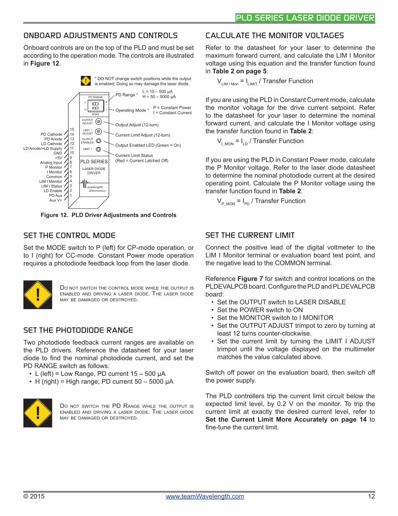
ONBOARD ADJUSTMENTS AND CONTROLS
Onboard controls are on the top of the PLD and must be set according to the operation mode. The controls are illustrated in Figure 12.
Electronicsavelength
PLD SERIES
P
L
PD RANGE
H
IMODE
Operating Mode *
Output Adjust (12-turn)
Current Limit Adjust (12-turn)
Output Enabled LED (Green = On)
Current Limit Status (Red = Current Latched Off)
PD Range *
L = 15 – 500 µAH = 50 – 5000 µA
P = Constant PowerI = Constant Current
LASER DIODEDRIVER
OUTPUTADJUST
LIMIT IADJUST
OUTPUTENABLED
LIMIT I
15
1
* DO NOT change switch positions while the output is enabled; Doing so may damage the laser diode.
PD CathodePD Anode
LD CathodeLD Anode/+LD Supply
GND+5V
Analog InputP MonitorI MonitorCommon
LIM I MonitorLIM I Status
LD EnablePD AuxAux V+
!
141312111098765432
Figure 12. PLD Driver Adjustments and Controls
SET THE CONTROL MODE
Set the MODE switch to P (left) for CP-mode operation, or to I (right) for CC-mode. Constant Power mode operation requires a photodiode feedback loop from the laser diode.
! Do noT swiTch The conTroL moDe whiLe The ouTpuT is enabLeD anD Driving a Laser DioDe. The Laser DioDe may be DamageD or DesTroyeD.
SET THE PHOTODIODE RANGE
Two photodiode feedback current ranges are available on the PLD drivers. Reference the datasheet for your laser diode to find the nominal photodiode current, and set the PD RANGE switch as follows:
• L (left) = Low Range, PD current 15 – 500 µA• H (right) = High range; PD current 50 – 5000 µA
! Do noT swiTch The pD range whiLe The ouTpuT is enabLeD anD Driving a Laser DioDe. The Laser DioDe may be DamageD or DesTroyeD.
CALCULATE THE MONITOR VOLTAGES
Refer to the datasheet for your laser to determine the maximum forward current, and calculate the LIM I Monitor voltage using this equation and the transfer function found in Table 2 on page 5:
VLIM I Mon = ILIMIT / Transfer Function
If you are using the PLD in Constant Current mode, calculate the monitor voltage for the drive current setpoint. Refer to the datasheet for your laser to determine the nominal forward current, and calculate the I Monitor voltage using the transfer function found in Table 2:
VI_MON = ILD / Transfer Function
If you are using the PLD in Constant Power mode, calculate the P Monitor voltage. Refer to the laser diode datasheet to determine the nominal photodiode current at the desired operating point. Calculate the P Monitor voltage using the transfer function found in Table 2:
VP_MON = IPD / Transfer Function
SET THE CURRENT LIMIT
Connect the positive lead of the digital voltmeter to the LIM I Monitor terminal or evaluation board test point, and the negative lead to the COMMON terminal.
Reference Figure 7 for switch and control locations on the PLDEVALPCB board. Configure the PLD and PLDEVALPCB board:
• Set the OUTPUT switch to LASER DISABLE• Set the POWER switch to ON• Set the MONITOR switch to I MONITOR• Set the OUTPUT ADJUST trimpot to zero by turning at
least 12 turns counter-clockwise.• Set the current limit by turning the LIMIT I ADJUST
trimpot until the voltage displayed on the multimeter matches the value calculated above.
Switch off power on the evaluation board, then switch off the power supply.
The PLD controllers trip the current limit circuit below the expected limit level, by 0.2 V on the monitor. To trip the current limit at exactly the desired current level, refer to Set the Current Limit More Accurately on page 14 to fine-tune the current limit.

© 2015 www.teamWavelength.com 13
PLD SERIES LASER DIODE DRIVER
ADJUST THE OUTPUT CURRENT SETPOINT— ONBOARD CONTROL
To increase the output current, turn the onboard trimpot clockwise; turn counter-clockwise to decrease output current.
While adjusting the output current, measure the voltage on pin 7, I Monitor. Use the transfer function listed in Table 2 to determine the output current from the monitor voltage.
ADJUST THE OUTPUT CURRENT SETPOINT— ANALOG INPUT
To use the Analog Input on pin 9 to adjust the output current, refer to Pin Descriptions on page 5 for specifications. The analog input signal sums with the onboard trimpot value.
Refer to the External Setpoint Circuit on page 15 for an example analog input circuit. Other circuits, a DAC signal, or function generator may be used.
COMBINING THE ONBOARD SETPOINT AND ANALOG INPUT
The Analog Input voltage signal on pin 9 sums with the onboard trimpot setpoint. This configuration allows the driver to be configured so that the laser current or power modulates around a DC setpoint.
If the sum of the two signals causes the PLD to attempt to drive the output current past the limit, the output will switch off and indicate a current limit error.
To avoid driving the current to the limit, first set the onboard trimpot to produce the Constant Current level. Then connect the modulation source to the Analog Input pin and slowly increase the modulation amplitude. Monitor the output current using the I Monitor pin, or by measuring the voltage across the test load. Do not monitor the voltage across a laser diode—measurement transients may damage the laser diode.
CURRENT LIMIT CIRCUIT TRIGGER AND RESET
If the PLD detects current limit, the output will switch off and the LIMIT I LED on the top of the unit will illuminate red. Set the Enable switch to OFF, correct the cause of the error, and then re-enable the output. Toggling the Output Current switch on the PLDEVALPCB board will clear the current limit latch.

© 2015 www.teamWavelength.com 14
PLD SERIES LASER DIODE DRIVER
REMOTE LIMIT STATUS LED CIRCUIT
The LIM I Status feature can be used to drive a remote LED up to 15 mA in your control system. Connect the LED as shown in Figure 13.
4LIM I Status
+5V 10
Figure 13. Remote LIM I Status LED
SET THE CURRENT LIMIT MORE ACCURATELY
The current limit circuit is designed with a small hysteresis, which causes the limit circuit to trip at a slightly lower current than calculated. To fine-tune the current limit, a small offset voltage must be factored in. Use this equation to calculate the hysteresis offset, where V+5V is the supply voltage:
Offset (V) = (V+5V – VI_MON) / 25.9
Then add the Offset to VLIMIT calculated on page 12.
CHANGE THE PHOTODIODE RANGE, TYPE A & B LASERS
The photodiode current range and transfer function can be adjusted by adding an external resistor. This feature is useful when the photodiode current of your laser falls in a range that does not allow maximum measurement sensitivity on the PLD driver.
Figure 14 shows the internal resistor network of the PLD and the equations explain the interaction with the external resistor.
14
6
PD RangeSwitch
554 Ω
5 kΩ
PD Range = L
µA
µA / V
PD Range = H
2.5 V * 106
R || 500 ΩRange = µA
µA / V6
R || 500 Ω10Transfer
Function =
2.5 V * 106
R || 5 kΩRange =
6
R || 5 kΩ10Transfer
Function =
R || 5 kΩR + 5000R * 5000= R || 500 Ω
R + 500R * 500=
PD Anode
COMMON
R
Internal Electronics External Electronics
ΩΩ
Figure 14. Adjusting the PD Range, Type A & B Lasers
CHANGE THE PHOTODIODE RANGE, TYPE C LASERS
The photodiode range and transfer function can be adjusted when using Type C lasers by connecting a ¼ W resistor between the PD Cathode (pin 15) and AUX V+ (pin 1).
The PD current range is calculated (units are amps):Range = 2.5 V / (R || 5 kΩ)
The transfer function is calculated (units are A / V): Transfer Function = 1 / (R || 5 kΩ)
The value of (R || 5 kΩ) is calculated as follows (units are Ω):(R || 5 kΩ) = (R * 5000) / (R + 5000)
ADDITIONAL TECHNICAL INFORMATIONThis section includes useful technical information on these topics:
• Remote Limit Status LED Circuit• Set the Current Limit More Accurately• Change the Photodiode Range, Type A & B Lasers• Change the Photodiode Range, Type C Lasers• Change the Analog Input Modulation Transfer Function• External Setpoint Circuit• • Ground the Fan on the PLD1250, PLD5000, and
PLD6500• Fine Tune Deep Modulation• Cable Lengths and High Current• Add Laser Diode Protection for Long Cables• Additional Noise Filtering• Monitor Calibration Circuit• Revision F Timing Characteristics• Product Variations• Output On/Off and Current Limit Timing• Safe Operating Area Calculation
© 2015 www.teamWavelength.com 15
PLD SERIES LASER DIODE DRIVER
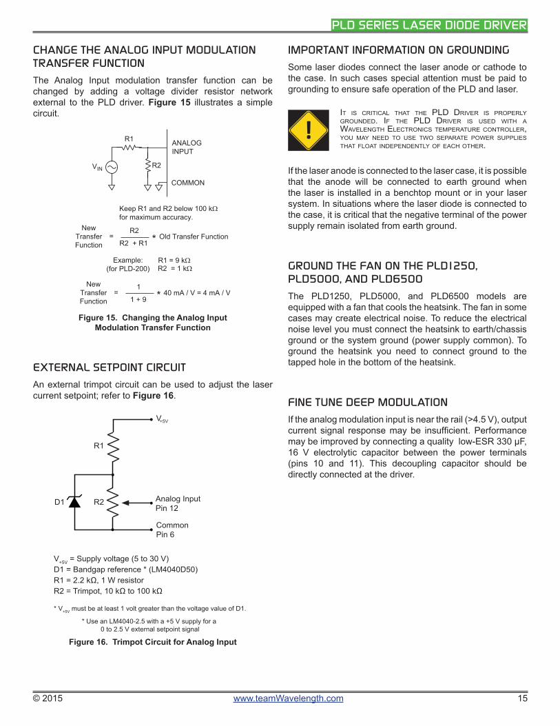
CHANGE THE ANALOG INPUT MODULATION TRANSFER FUNCTION
The Analog Input modulation transfer function can be changed by adding a voltage divider resistor network external to the PLD driver. Figure 15 illustrates a simple circuit.
R2
ANALOG INPUT
V
COMMON
Keep R1 and R2 below 100 kΩ for maximum accuracy.
IN
R1
R2 + R1
R2NewTransferFunction
Old Transfer Function= *
Example:(for PLD-200)
R1 = 9 kΩR2 = 1 kΩ
1 + 9
1NewTransferFunction
40 mA / V = 4 mA / V= *
Figure 15. Changing the Analog Input Modulation Transfer Function
EXTERNAL SETPOINT CIRCUIT
An external trimpot circuit can be used to adjust the laser current setpoint; refer to Figure 16.
R1
R2D1 Analog InputPin 12
V+5V
CommonPin 6
* Use an LM4040-2.5 with a +5 V supply for a 0 to 2.5 V external setpoint signal
* V+5V must be at least 1 volt greater than the voltage value of D1.
V+5V = Supply voltage (5 to 30 V)D1 = Bandgap reference * (LM4040D50)R1 = 2.2 kΩ, 1 W resistorR2 = Trimpot, 10 kΩ to 100 kΩ
Figure 16. Trimpot Circuit for Analog Input
IMPORTANT INFORMATION ON GROUNDING
Some laser diodes connect the laser anode or cathode to the case. In such cases special attention must be paid to grounding to ensure safe operation of the PLD and laser.
!iT is criTicaL ThaT The pLD Driver is properLy grounDeD. if The pLD Driver is useD wiTh a waveLengTh eLecTronics TemperaTure conTroLLer, you may neeD To use Two separaTe power suppLies ThaT fLoaT inDepenDenTLy of each oTher.
If the laser anode is connected to the laser case, it is possible that the anode will be connected to earth ground when the laser is installed in a benchtop mount or in your laser system. In situations where the laser diode is connected to the case, it is critical that the negative terminal of the power supply remain isolated from earth ground.
GROUND THE FAN ON THE PLD1250, PLD5000, AND PLD6500
The PLD1250, PLD5000, and PLD6500 models are equipped with a fan that cools the heatsink. The fan in some cases may create electrical noise. To reduce the electrical noise level you must connect the heatsink to earth/chassis ground or the system ground (power supply common). To ground the heatsink you need to connect ground to the tapped hole in the bottom of the heatsink.
FINE TUNE DEEP MODULATION
If the analog modulation input is near the rail (>4.5 V), output current signal response may be insufficient. Performance may be improved by connecting a quality low-ESR 330 µF, 16 V electrolytic capacitor between the power terminals (pins 10 and 11). This decoupling capacitor should be directly connected at the driver.
© 2015 www.teamWavelength.com 16
PLD SERIES LASER DIODE DRIVER
CABLE LENGTHS AND HIGH CURRENT
The length and gauge of cable from the power supply or to the laser diode can impact performance. The resistance and inductance of the wire can reduce bandwidth or cause the voltage to the PLD to droop.
If the output current starts to oscillate as setpoint voltage approaches the limit setting, then the power supply cables may be too long. If you cannot shorten the cables, place a 330 µF capacitor across pins 10 and 11 to minimize droop. Always twist the wire pairs to eliminate reactance.
ADD LASER DIODE PROTECTION FOR LONG CABLES
With a cable longer than two feet, add a Schottky diode across the laser diode, see Figure 17.
Laser Diode
SchottkyDiode
(1N5818)
Cable > 2 feet12
13
LD Anode
LD Cathode
Figure 17. Long Cable Laser Protection
ADDITIONAL NOISE FILTERING
The PLD drivers provide low-noise current to the laser diode, but in some cases additional filtering may be needed. Refer to Figure 18 for a simple and effective filter.
12
13
LD Anode
LD Cathode
SchottkyDiode
(1N5818)
0.1 µF
10 µF
Figure 18. PLD Output Filter
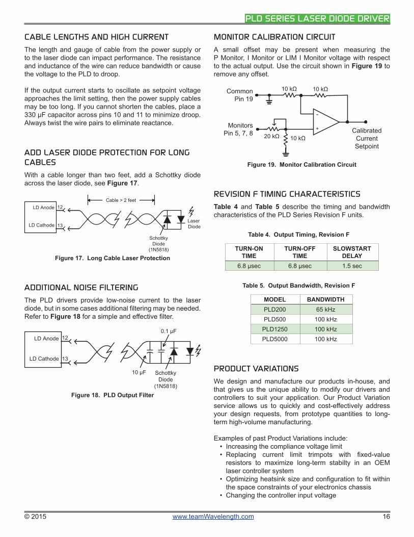
MONITOR CALIBRATION CIRCUIT
A small offset may be present when measuring the P Monitor, I Monitor or LIM I Monitor voltage with respect to the actual output. Use the circuit shown in Figure 19 to remove any offset.
CommonPin 19
+
10 kΩ
10 kΩ
10 kΩ
20 kΩ
-
MonitorsPin 5, 7, 8 Calibrated
CurrentSetpoint
Figure 19. Monitor Calibration Circuit
REVISION F TIMING CHARACTERISTICS
Table 4 and Table 5 describe the timing and bandwidth characteristics of the PLD Series Revision F units.
Table 4. Output Timing, Revision F
TURN-ON TIME
TURN-OFF TIME
SLOWSTART DELAY
6.8 µsec 6.8 µsec 1.5 sec
Table 5. Output Bandwidth, Revision F
MODEL BANDWIDTHPLD200 65 kHzPLD500 100 kHz
PLD1250 100 kHzPLD5000 100 kHz
PRODUCT VARIATIONS
We design and manufacture our products in-house, and that gives us the unique ability to modify our drivers and controllers to suit your application. Our Product Variation service allows us to quickly and cost-effectively address your design requests, from prototype quantities to long-term high-volume manufacturing. Examples of past Product Variations include:
• Increasing the compliance voltage limit• Replacing current limit trimpots with fixed-value
resistors to maximize long-term stabilty in an OEM laser controller system
• Optimizing heatsink size and configuration to fit within the space constraints of your electronics chassis
• Changing the controller input voltage
© 2015 www.teamWavelength.com 17
PLD SERIES LASER DIODE DRIVER
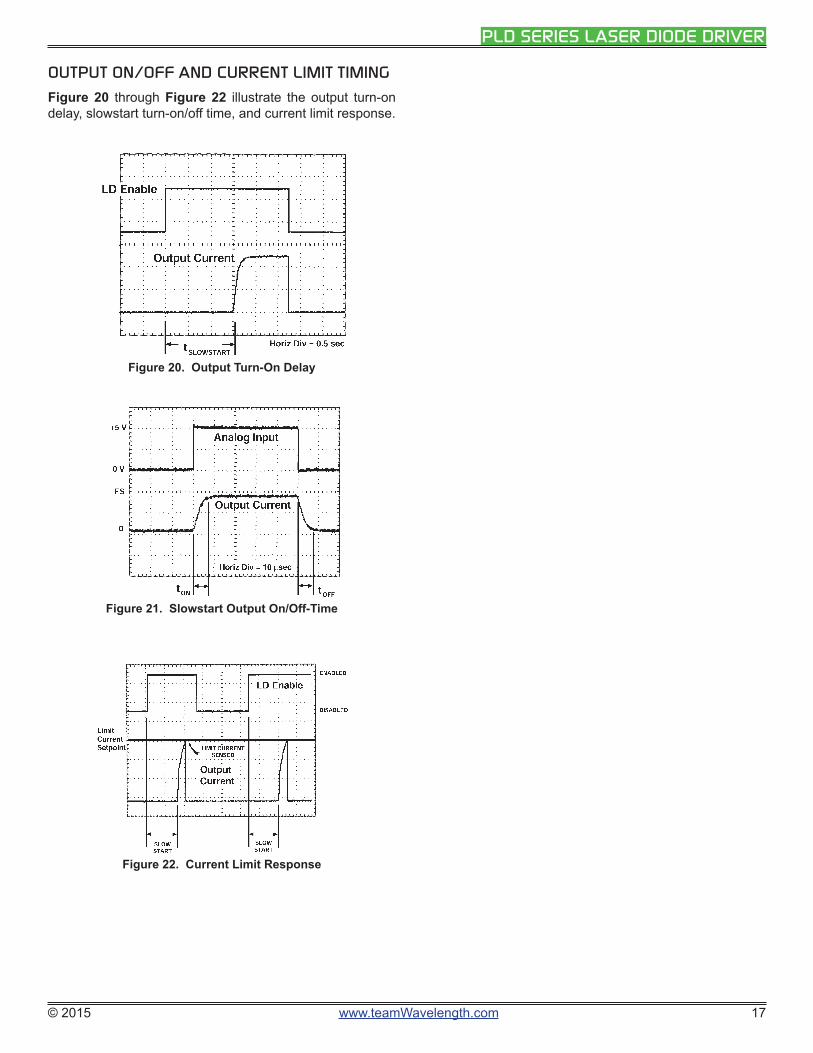
OUTPUT ON/OFF AND CURRENT LIMIT TIMING
Figure 20 through Figure 22 illustrate the output turn-on delay, slowstart turn-on/off time, and current limit response.
Figure 20. Output Turn-On Delay
Figure 21. Slowstart Output On/Off-Time
Figure 22. Current Limit Response

© 2015 www.teamWavelength.com 18
PLD SERIES LASER DIODE DRIVER
SAFE OPERATING AREA CALCULATION
The Safe Operating Area of the PLD driver is determined by the amount of power that can be dissipated within the output stage of driver. If that power limit is exceeded permanent damage can result.
!Do noT operaTe The pLD Driver ouTsiDe of The safe operaTing area curve.
operaTing The pLD Driver ouTsiDe of The soa voiDs The warranTy.
Refer to the Wavelength Electronics website for the most up-to-date SOA calculator for our products. The on-line tool is fast and easy to use, and also takes into consideration operating temperature.
http://www.teamwavelength.com/support/calculator/soa/soald.php
SOA charts are included in this datasheet for quick reference, however we recommend you use the on-line tools instead.
Follow these steps to determine if the driver will be operating within the SOA.
• Refer to the laser diode datasheet to find the maximum voltage (VMAX) and current (IMAX) specifications
• Calculate the voltage drop across the controller: VDROP = VS - VMAX (VS is the power supply voltage)
• Mark VDROP on the X-axis, and extend a line upward• Mark IMAX on the Y-axis, and extend a line to the right
until it intersects the VDROP line• On the X-axis, mark value of the VS • Extend a diagonal line from VS to the intersection of the
VDROP and IMAX lines; this is the Load Line• If the Load Line crosses the Safe Operating Area line at
any point, the configuration is not safe
If the SOA Calculator indicates the PLD will be outside of the Safe Operating Area, the system must be changed so that less power is dissipated within the driver. See Wavelength Electronics Application Note AN-LDTC01: The Principle of the Safe Operating Area for information on shifting the Load Line.
0.0 2.5 5.0 7.5 10.0 12.5 15.0 17.5 20.0 22.5 25.0 27.5 30.00.00
0.02
0.04
0.06
0.08
0.10
0.12
0.14
0.16
0.18
0.20
Voltage (V)
Cur
rent
(A)
Figure 23. SOA for PLD200
0.0 2.5 5.0 7.5 10.0 12.5 15.0 17.5 20.0 22.5 25.0 27.5 30.00.00
0.05
0.10
0.15
0.20
0.25
0.30
0.35
0.40
0.45
0.50
Voltage (V)
Cur
rent
(A)
Figure 24. SOA for PLD500
0.0 2.5 5.0 7.5 10.0 12.5 15.0 17.5 20.0 22.5 25.0 27.5 30.00.00
0.25
0.50
0.75
1.00
1.25
Voltage (V)
Cur
rent
(A)
Figure 25. SOA for PLD1250
0.0 2.5 5.0 7.5 10.0 12.5 15.0 17.5 20.0 22.5 25.0 27.5 30.00.00
1.00
2.00
3.00
4.00
5.00
Voltage (V)
Cur
rent
(A)
Figure 26. SOA for PLD5000
0.0 2.5 5.0 7.5 10.0 12.5 15.0 17.5 20.0 22.5 25.0 27.5 30.00.000.501.001.502.002.503.003.504.004.505.005.506.006.50
Voltage (V)
Cur
rent
(A)
Figure 27. SOA for PLD6500

© 2015 www.teamWavelength.com 19
PLD SERIES LASER DIODE DRIVER
TROUBLESHOOTING
PROBLEM POTENTIAL CAUSES SOLUTIONS
Driver will not switch on Improperly configured power supply
Carefully check the wiring diagram according to Table 3.
Output will not enable Remote Enable signal is not correct
Refer to the LD Enable specifications in Table 1 and make sure your input enable signal is correct.
Laser output power too low in Constant Current mode
Laser current setpoint too low Increase the setpoint either by adjusting the I SET trimpot clockwise, or by increasing the signal voltage on the Analog Input (pin 9).
Laser current limit too low Refer to page 12 for instructions on setting the laser driver current limit.
Laser driver is compliance limited
Check the laser diode specifications to determine the forward voltage (VF). Make sure that the PLD is not compliance limited. Refer to the Electrical Specifications table on page 6. If the driver is compliance limited, VLD ANODE may need to be increased. Verify that the PLD will be operating within the Safe Operating Area if VLD ANODE is increased.
Laser does not reach desired output in Constant Power mode
Current limit too low Check the laser diode datasheet to determine the approximate laser drive current at the desired optical power output level. Then verify that the current limit is set slightly higher than that. See page 12 for instructions on setting the laser driver current limit.
Photodiode feedback current is out of range for the PLD
Refer to the laser diode datasheet to determine the approximate photodiode (PD) current at the desired output power level. If the PD current exceeds the PLD PD current range, set the PD Range switch to High Range; see page 12.

© 2015 www.teamWavelength.com 20
PLD SERIES LASER DIODE DRIVER
MECHANICAL SPECIFICATIONS
1.10" [26.5mm]
1.52" [38.6mm]
1.72" [43.7mm]
2.65" [67.3mm]
0.75" [19.1mm]0.81" [20.6mm]
0.945" [24.0mm]
0.93" [23.6mm]
0.79" [20.1mm]
Elec
tro
nic
s
OU
TPU
TA
DJU
ST
LIM
IT I
ENA
BLE
DO
UTP
UT
avel
eng
th
PLD
SER
IES
LASE
R D
IOD
ED
RIVE
R
PLD1250, PLD5000, & PLD6500
1.77" [45.0mm]
PLD500 ONLY
0.58" [14.7mm]
1.49" [37.8mm]
0.58" [14.7mm]
PLD200 ONLY
PL
PD R
ANGE
H I
1 2
ON
MO
DE
AD
JUST
LIM
IT I
Figure 28. PLD Driver Mechanical Dimensions
4.40" [111.8mm]
3.40"[83.4mm]
4.00" [101.6mm]0.20" [5.1mm]0.20" [5.1mm]
3.00" [76.2mm]
3.57" [90.68mm]PLD1250, PLD5000,
& PLD65001 2
ON
Figure 29. PLDEVALPCB Board Mechanical Dimensions
Ø 0.125” [3.2mm]
Drill Ø0.1285 [3.27mm] clearance hole in PCB.Use 4-40 x ¼ to secure PLD to 0.062” thick PCB.
0.100” [25.4mm], TYP
0.30” [7.6mm]
0.025” [0.635mm] SQ pins (x15)Min Ø0.038” [0.965mm] hole in PCB
1.325” [33.6mm]
0.835” [21.2mm]
2.65” [67.3mm]
0.75” [19.1mm]
0.60”[15.2mm]
Pin 1
Figure 30. PLD PCB Layout Pattern, Top ViewAll Tolerances ±5%; units in inches [mm]
© 2015 www.teamWavelength.com 21
PLD SERIES LASER DIODE DRIVER
CERTIFICATION AND WARRANTY
CERTIFICATION
Wavelength Electronics, Inc. (Wavelength) certifies that this product met its published specifications at the time of shipment. Wavelength further certifies that its calibration measurements are traceable to the United States National Institute of Standards and Technology, to the extent allowed by that organization’s calibration facilities, and to the calibration facilities of other International Standards Organization members.
WARRANTY
This Wavelength product is warranted against defects in materials and workmanship for a period of one (1) year from date of shipment. During the warranty period, Wavelength will, at its option, either repair or replace products which prove to be defective.
WARRANTY SERVICE
For warranty service or repair, this product must be returned to the factory. An RMA is required for products returned to Wavelength for warranty service. The Buyer shall prepay shipping charges to Wavelength and Wavelength shall pay shipping charges to return the product to the Buyer upon determination of defective materials or workmanship. However, the Buyer shall pay all shipping charges, duties, and taxes for products returned to Wavelength from another country.
LIMITATIONS OF WARRANTY
The warranty shall not apply to defects resulting from improper use or misuse of the product or operation outside published specifications. No other warranty is expressed or implied. Wavelength specifically disclaims the implied warranties of merchantability and fitness for a particular purpose.
EXCLUSIVE REMEDIES
The remedies provided herein are the Buyer’s sole and exclusive remedies. Wavelength shall not be liable for any direct, indirect, special, incidental, or consequential damages, whether based on contract, tort, or any other legal theory.
REVERSE ENGINEERING PROHIBITED
Buyer, End-User, or Third-Party Reseller are expressly prohibited from reverse engineering, decompiling, or disassembling this product.
NOTICE
The information contained in this document is subject to change without notice. Wavelength will not be liable for errors contained herein or for incidental or consequential damages in connection with the furnishing, performance, or use of this material. No part of this document may be translated to another language without the prior written consent of Wavelength.
SAFETY
There are no user-serviceable parts inside this product. Return the product to Wavelength Electronics for service and repair to ensure that safety features are maintained.
LIFE SUPPORT POLICY
This important safety information applies to all Wavelength electrical and electronic products and accessories:
As a general policy, Wavelength Electronics, Inc. does not recommend the use of any of its products in life support applications where the failure or malfunction of the Wavelength product can be reasonably expected to cause failure of the life support device or to significantly affect its safety or effectiveness. Wavelength will not knowingly sell its products for use in such applications unless it receives written assurances satisfactory to Wavelength that the risks of injury or damage have been minimized, the customer assumes all such risks, and there is no product liability for Wavelength. Examples of devices considered to be life support devices are neonatal oxygen analyzers, nerve stimulators (for any use), auto-transfusion devices, blood pumps, defibrillators, arrhythmia detectors and alarms, pacemakers, hemodialysis systems, peritoneal dialysis systems, ventilators of all types, and infusion pumps as well as other devices designated as “critical” by the FDA. The above are representative examples only and are not intended to be conclusive or exclusive of any other life support device.
REVISION HISTORY
DOCUMENT NUMBER: PLD5000-00400
REV. DATE CHANGE
P November 2013
Added CE icon and extended warranty
Q January 2014 Updated CP test load section
R October 2015
Added Disable Fall Time specification
WAVELEnGTH E L E C T R O N I C S
51 Evergreen DriveBozeman, Montana 59771
406-587-4910 (tel)406-587-4911 (fax)
Sales & Tech [email protected]