datasheet - intersil.com€¢ sample and hold circuits • digital filters • operational amplifier...
TRANSCRIPT

FN3123Rev 4.00
September 2004
HI-201HSHigh Speed, Quad SPST, CMOS Analog Switch
DATASHEET
The HI-201HS is a monolithic CMOS Analog Switch featuring very fast switching speeds and low ON resistance. The integrated circuit consists of four independently selectable SPST switches and is pin compatible with the industry standard HI-201 switch.
Fabricated using silicon-gate technology and the Intersil Dielectric Isolation process, this TTL compatible device offers improved performance over previously available CMOS analog switches. Featuring maximum switching times of 50ns, low ON resistance of 50 maximum, and a wide analog signal range, the HI-201HS is designed for any application where improved switching performance, particularly switching speed, is required. (A more detailed discussion on the design and application of the HI-201HS can be found in Application Note AN543.)
Features
• Fast Switching Times
- tON . . . . . . . . . . . . . . . . . . . . . . . . . . . . . . . . . . . . 30ns
- tOFF . . . . . . . . . . . . . . . . . . . . . . . . . . . . . . . . . . . 40ns
• Low “ON” Resistance . . . . . . . . . . . . . . . . . . . . . . . . 30
• Pin Compatible with Standard HI-201
• Wide Analog Voltage Range (15V Supplies) . . . . . . . 15V
• Low Charge Injection (15V Supplies) . . . . . . . . . . 10pC
• TTL Compatible
• Symmetrical Switching Analog Current Range . . . . . 80mA
Applications
• High Speed Multiplexing
• High Frequency Analog Switching
• Sample and Hold Circuits
• Digital Filters
• Operational Amplifier Gain Switching Networks
• Integrator Reset Circuits
Pinout (Switches Shown For Logic “1” Input)
HI-201HS (CERDIP, PDIP, SOIC)TOP VIEW
Ordering Information
PART NUMBERTEMP.
RANGE (oC) PACKAGEPKG. NO.
HI1-0201HS-2 -55 to 125 16 Ld CERDIP F16.3
HI1-0201HS-4 -25 to 85 16 Ld CERDIP F16.3
HI1-0201HS-5 0 to 75 16 Ld CERDIP F16.3
HI3-0201HS-5 0 to 75 16 Ld PDIP E16.3
HI9P0201HS-5 0 to 75 16 Ld SOIC M16.3
HI9P0201HS-9 -40 to 85 16 Ld SOIC M16.3
14
15
16
9
13
12
11
10
1
2
3
4
5
7
6
8
A1
OUT1
IN1
V-
GND
IN4
A4
OUT4
A2
IN2
V+
NC
IN3
OUT3
A3
OUT2
FN3123 Rev 4.00 Page 1 of 12September 2004

HI-201HS
Functional Diagram
TTLLOGICINPUT
SWITCHCELL
LEVELSHIFTER
ANDDRIVER
GATE
SOURCE
DRAIN
GATE
INPUT
OUTPUT
V-
V+
TRUTH TABLE
LOGIC SWITCH
01
ONOFF
Schematic Diagrams
TTL/CMOS REFERENCE CIRCUIT SWITCH CELL
P41
V+MP42
MP43 MP44
QP44
QN44
QN45
C49
C48
VR1
QN43
R42
R41
QN41
QN42
D415V
D425.6V
QP42
QP41
V-
MN42 MN44 MN45
MP45
MP31
MN32
MP33
MN33
MN31
MP32
ANALOGIN
ANALOGOUT
Q
Q
V-
V+
FN3123 Rev 4.00 Page 2 of 12September 2004
HI-201HS
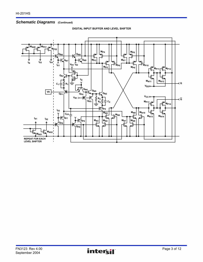
DIGITAL INPUT BUFFER AND LEVEL SHIFTER
Schematic Diagrams (Continued)
MN46 MP51
IQ IX3 IX4IX1
QN6
QN7
VR1 IX2
IX3
QP7
QP6
MN52MN51
IX1 IX2
REPEAT FOR EACHLEVEL SHIFTER
QN1
C1 R1
QP1
IQ
QN4
QN8
QN9 MP3
MP4
QP9
QP8
MP5
MP7
CFF
C2
QN2
QN5
QP2
R3R2
QP5
QP4
VR1
MP9MP6 MP10
MN3 MN4
MN5MN6
MP8
MN7 MN8
MN10MN9
MP11
MN11
VEE
MP12
MN12Q
MP13
MN13
VCC
MP14
MN14
Q
MP52
VA
FN3123 Rev 4.00 Page 3 of 12September 2004

HI-201HS
Absolute Maximum Ratings Thermal Information
Supply Voltage (V+ to V-). . . . . . . . . . . . . . . . . . . . . . . . . . . . . . 36VDigital Input Voltage . . . . . . . . . . . . . . . . . . . . . . (V+) +4V to (V-) -4VAnalog Input Voltage (One Switch) . . . . . . . (V+) +2.0V to (V-) -2.0VPeak Current, S or D (Pulse 1ms, 10% Duty Cycle Max) . . . . 50mAContinuous Current Any Terminal (Except S or D) . . . . . . . . . 25mA
Operating ConditionsTemperature Ranges HI-201HS-2 . . . . . . . . . . . . . . . . . . . . . . . . . . . . . -55oC to 125oC HI-201HS-4 . . . . . . . . . . . . . . . . . . . . . . . . . . . . . . -25oC to 85oC HI-201HS-5 . . . . . . . . . . . . . . . . . . . . . . . . . . . . . . . . 0oC to 75oC HI-201HS-9 . . . . . . . . . . . . . . . . . . . . . . . . . . . . . . -40oC to 85oC
Thermal Resistance (Typical, Note 1) JA (oC/W) JC (oC/W)
CERDIP Package. . . . . . . . . . . . . . . . . 80 20 PDIP Package . . . . . . . . . . . . . . . . . . . 90 N/A SOIC Package . . . . . . . . . . . . . . . . . . . 100 N/AMaximum Junction Temperature Ceramic Package. . . . . . . . . . . . . . . . . . . . . . . . . . . . . . . . 175oC Plastic Package . . . . . . . . . . . . . . . . . . . . . . . . . . . . . . . . . 150oCMaximum Storage Temperature. . . . . . . . . . . . . . . . -65oC to 150oCMaximum Lead Temperature (Soldering 10s) . . . . . . . . . . . . 300oC (SOIC - Lead Tips Only)
CAUTION: Stresses above those listed in “Absolute Maximum Ratings” may cause permanent damage to the device. This is a stress only rating and operation of the device at these or any other conditions above those indicated in the operational sections of this specification is not implied.
NOTE:
1. JA is measured with the component mounted on an evaluation PC board in free air.
Electrical Specifications Supplies = +15V, -15V; VAH (Logic Level High) = 2.4V, VAL (Logic Level Low) = +0.8V, GND = 0V,Unless Otherwise Specified
PARAMETERTEST
CONDITIONSTEMP(oC)
-2 -4, -5, -9
UNITSMIN TYP MAX MIN TYP MAX
DYNAMIC CHARACTERISTICS
Switch ON Time, tON (Note 3) 25 - 30 50 - 30 50 ns
Switch OFF Time, tOFF1 (Note 3) 25 - 40 50 - 40 50 ns
Switch OFF Time, tOFF2 (Note 3) 25 - 150 - - 150 - ns
Output Settling Time To 0.1% 25 - 180 - - 180 - ns
Charge Injection, Q (Note 6) 25 - 10 - - 10 - pC
OFF Isolation (Note 4) 25 - 72 - - 72 - dB
Crosstalk (Note 5) 25 - 86 - - 86 - dB
Input Switch Capacitance, CS(OFF) 25 - 10 - - 10 - pF
Output Switch Capacitance CD(OFF) 25 - 10 - - 10 - pF
CD(ON) 25 - 30 - - 30 - pF
Digital Input Capacitance, CA 25 - 18 - - 18 - pF
Drain-To-Source Capacitance, CDS(OFF) 25 - 0.5 - - 0.5 - pF
DIGITAL INPUT CHARACTERISTICS
Input Low Threshold, VAL Full - - 0.8 - - 0.8 V
Input High Threshold, VAH 25 2.0 - - 2.0 - - V
Full 2.4 - - 2.4 - - V
Input Leakage Current (Low), IAL 25 - 200 - - 200 - A
Full - - 500 - - 500 A
Input Leakage Current (High), IAH VAH = 4.0V 25 - 20 - - 20 - A
Full - - 40 - - 40 A
ANALOG SWITCH CHARACTERISTICS
Analog Signal Range, VS Full -15 - +15 -15 - +15 V
ON Resistance, rON (Note 2) 25 - 30 50 - 30 50
Full - - 75 - - 75
FN3123 Rev 4.00 Page 4 of 12September 2004
HI-201HS
rON Match 25 - 3 - - 3 - %
OFF Input Leakage Current, IS(OFF) 25 - 0.3 10 - 0.3 10 nA
Full - - 100 - - 50 nA
OFF Output Leakage Current, ID(OFF) 25 - 0.3 10 - 0.3 10 nA
Full - - 100 - - 50 nA
ON Leakage Current, ID(ON) 25 - 0.1 10 - 0.1 10 nA
Full - - 100 - - 50 nA
POWER SUPPLY CHARACTERISTICS (Note 7)
Power Dissipation, PD 25 - 120 - - 120 - mW
Full - - 240 - - 240 mW
Current, I+ (Pin 13) 25 - 4.5 - - 4.5 - mA
Full - - 10.0 - - 10.0 mA
Current, I- (Pin 4) 25 - 3.5 - - 3.5 - mA
Full - - 6 - - 6 mA
NOTES:
2. VOUT = 10V, IOUT = 1mA.
3. RL = 1k , CL = 35pF, VIN = +10V, VA = +3V. (See Figure 1).
4. VA = 3V, RL = 1k , CL = 10pF, VIN = 3VRMS , f = 100kHz.
5. VA = 3V, RL = 1k , VIN = 3VRMS , f = 100kHz.
6. CL = 1nF, VIN = 0V, Q = CL x VO .
7. VA = 3V or VA = 0 for all switches.
Electrical Specifications Supplies = +15V, -15V; VAH (Logic Level High) = 2.4V, VAL (Logic Level Low) = +0.8V, GND = 0V,Unless Otherwise Specified (Continued)
PARAMETERTEST
CONDITIONSTEMP(oC)
-2 -4, -5, -9
UNITSMIN TYP MAX MIN TYP MAX
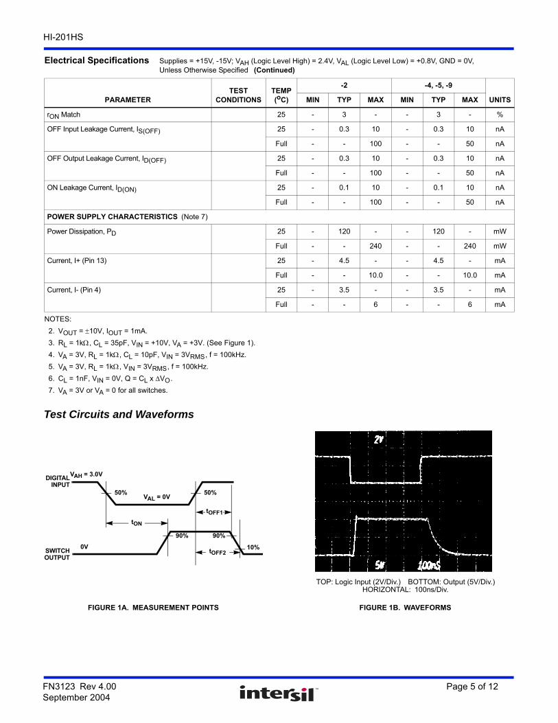
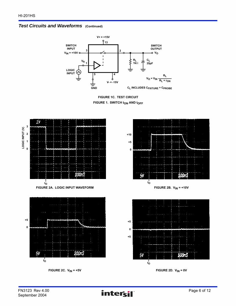
Test Circuits and Waveforms
FIGURE 1A. MEASUREMENT POINTS FIGURE 1B. WAVEFORMS
DIGITALINPUT
SWITCHOUTPUT
VAH = 3.0V
50%VAL = 0V
90%
10%
tON
50%
0V
90%
tOFF2
tOFF1
TOP: Logic Input (2V/Div.) BOTTOM: Output (5V/Div.)HORIZONTAL: 100ns/Div.
FN3123 Rev 4.00 Page 5 of 12September 2004
HI-201HS
FIGURE 1C. TEST CIRCUIT
FIGURE 1. SWITCH tON AND tOFF
FIGURE 2A. LOGIC INPUT WAVEFORM FIGURE 2B. VIN = +10V
FIGURE 2C. VIN = +5V FIGURE 2D. VIN = 0V
Test Circuits and Waveforms (Continued)
VO3
1
LOGICINPUT
VIN = +10V
RL1k
CL35pF
SWITCHOUTPUT
V+ = +15V
13
V- = -15V
4
SWITCHINPUT
GND
VO = VIN
RL
RL + rON
2
5
VA
CL INCLUDES CFIXTURE + CPROBE
3
2
1
0
tO
LO
GIC
IN
PU
T (
V)
+10
+5
0
tO
+5
0
tO
+5
0
+5
tO
FN3123 Rev 4.00 Page 6 of 12September 2004
HI-201HS
Application Information
Logic Compatibility
The HI-201HS is TTL compatible. Its logic inputs (pins 1, 8, 9, and 16) are designed to react to digital inputs which exceed a fixed, internally generated TTL switching threshold. The HI-201HS can also be driven with CMOS logic (0V-15V), although the switch performance with CMOS logic will be inferior to that with TTL logic (0V-5V).
The logic input design of the HI-201HS is largely responsible for its fast switching speed. It is a design which features a unique input stage consisting of complementary vertical PNP and NPN bipolar transistors. This design differs from that of the standard HI-201 product where the logic inputs are MOS transistors.
Although the new logic design enhances the switching speed performance, it also increases the logic input leakage currents. Therefore, the HI-201HS will exhibit larger digital input leakage currents in comparison to the standard HI-201 product.
Charge Injection
Charge injection is the charge transferred, through the internal gate-to-channel capacitances, from the digital logic input to the analog output. To optimize charge injection performance for the HI-201HS, it is advisable to provide a TTL logic input with fast rise and fall times.
If the power supplies are reduced from 15V, charge injection will become increasingly dependent upon the digital input frequency. Increased logic input frequency will result in larger output error due to charge injection.
Power Supply Considerations
The electrical characteristics specified in this data sheet are guaranteed for power supplies VS = 15V. Power supply voltages less than 15V will result in reduced switch performance. The following information is intended as a design aid only.
Single Supply
The switch operation of the HI-201HS is dependent upon an internally generated switching threshold voltage optimized for 15V power supplies. The HI-201HS does not provide the necessary internal switching threshold in a single supply system. Therefore, if single supply operation is required, the HI-300 series of switches is recommended. The HI-300 series will remain operational to a minimum +5V single supply.
Switch performance will degrade as power supply voltage is reduced from optimum levels (15V). So it is recommended that a single supply design be thoroughly evaluated to ensure that the switch will meet the requirements of the application.
For further information see Application Notes AN520, AN521, AN531, AN532, AN543 and AN557.
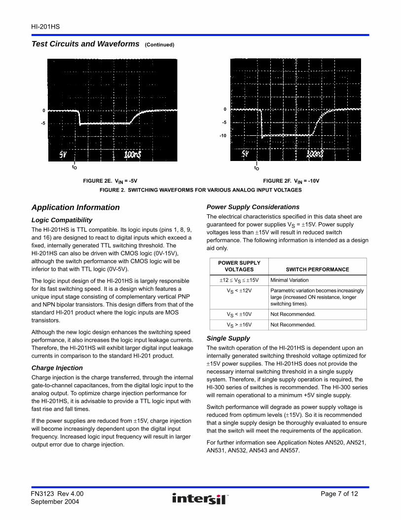
FIGURE 2E. VIN = -5V FIGURE 2F. VIN = -10V
FIGURE 2. SWITCHING WAVEFORMS FOR VARIOUS ANALOG INPUT VOLTAGES
Test Circuits and Waveforms (Continued)
0
-5
tO
-10
-5
0
tO
POWER SUPPLYVOLTAGES SWITCH PERFORMANCE
12 VS 15V Minimal Variation
VS < 12V Parametric variation becomes increasingly large (increased ON resistance, longer switching times).
VS < 10V Not Recommended.
VS > 16V Not Recommended.
FN3123 Rev 4.00 Page 7 of 12September 2004

HI-201HS
Typical Performance Curves
FIGURE 3. ON RESISTANCE vs ANALOG SIGNAL LEVEL FIGURE 4. ON RESISTANCE vs ANALOG SIGNAL LEVEL
FIGURE 5. IS(OFF) OR ID(OFF) vs TEMPERATURE † FIGURE 6. ID(ON) vs TEMPERATURE †
† Theoretically, leakage current will continue to decrease below 25oC. But due to environmental conditions, leakage measurements below this temperature are not representative of actual switch performance.
FIGURE 7. SUPPLY CURRENT vs TEMPERATURE FIGURE 8. LEAKAGE CURRENT vs ANALOG INPUT VOLTAGE
-15 -10 -5 0 5 10 15
80
70
60
50
40
30
20
10
0
125oC
V+ = +15V, V- = -15V
25oC
-55oC
ANALOG INPUT (V)
ON
RE
SIS
TAN
CE
(
)
-15 -10 -5 0 5 10 15
80
70
60
50
40
30
20
10
0
V+ = +12V, V- = -12V
TA = 25oC
ANALOG INPUT (V)
ON
RE
SIS
TAN
CE
(
)
V+ = +15V, V- = -15V
V+ = +8V, V- = -8V
V+ = +10V, V- = -10V
25 75 125
TEMPERATURE (oC)
0.01
0.10
1.0
10.0
100.0
LE
AK
AG
E C
UR
RE
NT
(n
A)
25 75 125
TEMPERATURE (oC)
0.01
0.10
1.0
10.0
100.0
LE
AK
AG
E C
UR
RE
NT
(n
A)
TEMPERATURE (oC)
125105856545255-15-35-55
7
6
5
4
3
2
1
0
SU
PP
LY C
UR
RE
NT
(m
A)
V+ = +15V, V- = -15V
I+
I-
14121086420-2-4-6-8-10-12-14ANALOG INPUT (V)
LE
AK
AG
E C
UR
RE
NT
(p
A)
10080604020
0-20-40-60-80
-100-120-140-160-180-200
IDON
V+ = +15V, V- = -15VIS(OFF) VD = 0VID(OFF) VS = 0V
IS(OFF)/ID(OFF)
FN3123 Rev 4.00 Page 8 of 12September 2004

HI-201HS
FIGURE 9. DIGITAL INPUT LEAKAGE CURRENT vsTEMPERATURE †
FIGURE 10. LEAKAGE CURRENT vs ANALOG INPUT VOLTAGE
† Theoretically, leakage current will continue to decrease below 25oC. But due to environmental conditions, leakage measurements below this temperature are not representative of actual switch performance.
FIGURE 11. SWITCHING TIME vs TEMPERATURE FIGURE 12. SWITCHING TIME vs SUPPLY VOLTAGE
FIGURE 13. SWITCHING TIME vs POSITIVE SUPPLY VOLTAGE FIGURE 14. SWITCHING TIME vs NEGATIVE SUPPLY VOLTAGE
Typical Performance Curves (Continued)
TEMPERATURE (oC)
12511510595857565554525
VAL = 0V, VAH2 = 3V, VAH1 = 5V
35
6040200
-20-40-60-80
-100-120-140-160-180-200-220-240-260-280
LE
AK
AG
E C
UR
RE
NT
(A
)
IAH1
IAH2
IAL
16.015.515.014.5-14.0-14.5-15.0-15.5-16.0 14.0
ANALOG INPUT (V)
109876543210
-1-2-3-4-5-6-7-8-9
-10
V+ = +15V, V- = -15V, TA = 25oCIS(OFF) VD = 0VID(OFF) VS = 0V
LE
AK
AG
E C
UR
RE
NT
(n
A)
TEMPERATURE (oC)
125105856545255-15-35-55
180
160
140
120
100
80
60
40
20
0
SW
ITC
HIN
G T
IME
(n
s)
tOFF2
tOFF1
tON
V+ = +15VV- = -15VRL = 1kCL = 35pF
SUPPLY VOLTAGE (V)
RL = 1k, CL = 35pF, TA = 25oC
tOFF2
tOFF1tON
5 6 7 8 9 10 11 12 13 14 15
350
300
250
200
150
100
50
0
SW
ITC
HIN
G T
IME
(n
s)
POSITIVE SUPPLY (V)
V- = -15V, RL = 1k
tOFF2
tOFF1
tON
5 6 7 8 9 10 11 12 13 14 15
350
300
250
200
150
100
50
SW
ITC
HIN
G T
IME
(n
s)
CL = 35pF, TA = 25oC
0
NEGATIVE SUPPLY (V)
tOFF2
tOFF1
tON
-5 -6 -7 -8 -9 -10 -11 -12 -13 -14 -15
350
300
250
200
150
100
50
0
SW
ITC
HIN
G T
IME
(n
s)
V+ = +15V, RL = 1kCL = 35pF, TA = 25oC
FN3123 Rev 4.00 Page 9 of 12September 2004

HI-201HS
FIGURE 15. SWITCHING TIME vs INPUT LOGIC VOLTAGE FIGURE 16. INPUT SWITCHING THRESHOLD vs SUPPLY VOLTAGE
FIGURE 17. CHARGE INJECTION vs ANALOG VOLTAGE FIGURE 18. CAPACITANCE vs ANALOG VOLTAGE
FIGURE 19. OFF ISOLATION vs FREQUENCY FIGURE 20. CROSSTALK vs FREQUENCY
Typical Performance Curves (Continued)
DIGITAL INPUT VOLTAGE (V)
tOFF2
tOFF1tON
0 1 2 3 4 5
350
300
250
200
150
100
50
0
SW
ITC
HIN
G T
IME
(n
s)
V + = +15V, V- = -15V, RL = 1k
CL = 35pF, VAL = 0V, TA = 25oC
SUPPLY VOLTAGE (V)
10 11 12 13 14 15987650
3.0
2.5
2.01.8
1.5
1.0
0.5INP
UT
LO
GIC
TH
RE
SH
OL
D (
V)
ANALOG INPUT (V)
-10 -5 0 5 10
-10
-20
-30
-40
-50
50
40
30
20
10
0
V+ = +15V, V- = -15V
CL = 1nF
Q
VA
CL
IN OUT VO
Q = CL x VO
CH
AR
GE
IN
JE
CT
ION
(p
C)
ANALOG INPUT (V)
-15 -5 0 5 15
40
CD(ON)
10-10
CD(OFF) OR CS(OFF)
CDS(OFF)
35
30
25
20
15
10
5
0
CA
PA
CIT
AN
CE
(p
F)
V+ = +15V, V- = -15V
VIN = 3VRMS, VA = 3V
RL = 100
RL = 1kRL
IN OUT
VIN
VO
OFF ISOLATION = 20 LogVIN
VO
FREQUENCY (Hz)
10M1M100K10K
140
120
100
80
60
40
20
0
OF
F I
SO
LA
TIO
N (
dB
)
FREQUENCY (Hz)
10M1M100K10K
140
120
100
80
60
40
20
0
CR
OS
STA
LK
(d
B)
V+ = +15V, V- = -15V
VIN = 3VRMS, VA = 3V
RL = 1k
IN OUT
VIN
VO1
CROSSTALK = 20 LogVO2
VO1
VO2
RL = 1k
FN3123 Rev 4.00 Page 10 of 12September 2004

HI-201HS
Intersil products are manufactured, assembled and tested utilizing ISO9001 quality systems as notedin the quality certifications found at www.intersil.com/en/support/qualandreliability.html
Intersil products are sold by description only. Intersil may modify the circuit design and/or specifications of products at any time without notice, provided that such modification does not, in Intersil's sole judgment, affect the form, fit or function of the product. Accordingly, the reader is cautioned to verify that datasheets are current before placing orders. Information furnished by Intersil is believed to be accurate and reliable. However, no responsibility is assumed by Intersil or its subsidiaries for its use; nor for any infringements of patents or other rights of third parties which may result from its use. No license is granted by implication or otherwise under any patent or patent rights of Intersil or its subsidiaries.
For information regarding Intersil Corporation and its products, see www.intersil.com
For additional products, see www.intersil.com/en/products.html
© Copyright Intersil Americas LLC 2004. All Rights Reserved.All trademarks and registered trademarks are the property of their respective owners.
Die Characteristics
DIE DIMENSIONS
2440m x 2860m x 485m
METALLIZATION
Type: CuAlThickness: 16kÅ 2kÅ
PASSIVATION
Type: Nitride Over SiloxNitride Thickness: 3.5kÅ 1kÅSilox Thickness: 12kÅ 2kÅ
WORST CASE CURRENT DENSITY
9.5 x 10⁴ A/cm2
FN3123 Rev 4.00 Page 11 of 12September 2004
HI-201HS
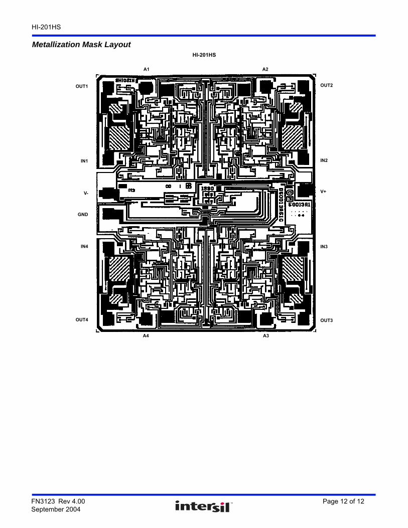
Metallization Mask LayoutHI-201HS
A1 A2
OUT2
IN2
V+
IN3
OUT3
A3A4
OUT4
IN4
GND
V-
IN1
OUT1
FN3123 Rev 4.00 Page 12 of 12September 2004