dc/ac inverter based switched capacitor topology · the main idea is to utilise a simple circuit...
TRANSCRIPT

DC/AC Inverter based Switched Capacitor Topology
Department of Electronics and Computer Engineering
College of Engineering, Design and Physical Sciences
Brunel University, London, UK
By
Mohd Helmy Hakimie Bin Mohd Rozlan
A thesis Submitted for the degree of Doctor of Philosophy
Supervised
By:
Dr Mohamed Darwish
April, 2017

II
Abstract
This thesis presents a new DC/AC inverter circuit which is based on a
switched-capacitor circuit topology with reduced components (power switch and
capacitor) count for low power applications. The proposed circuit has distinct features
of both voltage boost-up and near sinusoidal (multi-level/staircase) AC output voltage.
The main idea is to utilise a simple circuit technique called resonant-based Double
Switch Single Capacitor Switched-Capacitor (DSSC SCC) with variable duty cycle
Pulse Width Modulation (PWM) control technique in such a way that multi-level
voltage can be realised across a capacitor. In order to show the superiority of the
applied technique, comparisons with other techniques/circuits configurations are
presented. The circuit technique can significantly reduce the number of multiple stages
of switched-capacitor circuit cells of the recent switched-capacitor multi-level inverter
topology. The proposed inverter (with integrated DSSC SCC technique) can generate
a line-frequency with 13-levels near sinusoidal AC output voltage with low total
harmonics distortion. The output voltage can be achieved with the least number of
components use and only a single DC source is used as an input. The proposed inverter
topology is also reviewed against other inverter-based switched-capacitor circuit
topology and the well-known multi-level inverter topology. The proposed inverter has
shown a tremendous reduction in the total harmonics distortion and circuit component
count in comparison with the recent Switched-Capacitor Boost multi-level inverter and
the classical Cascaded H-Bridge multi-level inverter. Mathematical analysis shows the
design of the proposed inverter and PSPICE simulation result to verify the design is
also presented. The practical experiment implementation of the proposed system is
presented and proves the correct operation of the proposed inverter topology by
showing consistency between simulation results and practical results.

III
I dedicate this thesis to
My Parents, Mohd Rozlan Abd Ghapar, Aznah Abdul Aziz,
lovely wife, Dr Nurul Syuhada Ramli
Son, Muhammad Ammar Harith,
Brothers and Sister, Afiq Azali, Afiq Farhan, Zarul Izham, Farra
Nadia,
& Humanity and My home country, Malaysia

IV
Acknowledgments
First, I would like to thank Almighty Allah, the one who granted me a long life,
and who always supported and blessed me with strength and good health. I also would
like to thank my supervisor Dr Mohamed Darwish for his kindest guidance and
assistance during my PhD study. He is a helpful advisor and the best instructor for the
achievement of this thesis. I would like to special my thanks to Dr Christos Marouchos,
Dr Michael Theoridis and Dr Maysam Abbod for their kind support and help.
I also thank the friendly staff and my research group colleagues at the Brunel
Institute of Power Systems (BIPS) for their support and friendship.
Great thanks to my family, especially my fathers, my mothers, my brothers and
sisters for their prayers, patience, and emotional support throughout conducting this
research. Special thanks to my beloved wife, Dr Nurul Syuhada Ramli and son,
Muhammad Ammar Harith, for their patience and emotional support.

V
Table of Contents
Abstract ................................................................................................... II
Acknowledgments ................................................................................. IV
Table of Contents ................................................................................... V
List of Tables ...................................................................................... VIII
List of Figures ......................................................................................... X
List of Symbols ................................................................................... XIV
List of Abbreviations ....................................................................... XVII
Chapter 1 Introduction ........................................................................... 1
Overview .......................................................................................................... 1
Research Question ............................................................................................ 4
Research Motivation ........................................................................................ 5
Research Aim and Objectives .......................................................................... 6
1.4.1 Research Approach .......................................................................................... 7
1.4.2 Contributions to Knowledge ............................................................................ 7
1.4.3 Thesis Overview and Structure ........................................................................ 9
Chapter 2 Literature Review of DC/AC Inverters ............................ 11
Introduction .................................................................................................... 11
Classification of DC/AC Inverter Circuit ....................................................... 11
2.2.1 Voltage Source Inverter ................................................................................. 14
2.2.2 Current Source Inverter .................................................................................. 17
2.2.3 Impedance Source Inverter ............................................................................. 19
2.2.4 Classical Multi-Level Inverter Topologies .................................................... 23
2.2.5 Improving THD in CHB-MLI circuit topology ............................................. 33
Summary of PWM Inverters & Multi-Level Inverter topologies .................. 38
Summary ........................................................................................................ 42

VI
Chapter 3 Switched-Capacitor Circuit & Switched-Capacitor Multi-level DC/AC Inverter Topologies ........................................................ 43
Introduction .................................................................................................... 43
Overview of Voltage Boosting Technique ..................................................... 44
Switched Capacitor ........................................................................................ 46
3.3.1 Resonant-based Double Switch Single Capacitor (DSSC) circuit ................. 50
3.3.2 Resonant-based Double Switch Double Capacitor (DSDC) circuit ............... 65
3.3.3 Resonant-based Single Switch Single Capacitor (SSSC) circuit. .................. 67
3.3.4 Resonant-based Triplen switch SCC circuit ................................................... 68
3.3.5 Capacitor-based switched-capacitor circuit in series-parallel connection ..... 70
Other Voltage Boosting Techniques .............................................................. 73
3.4.1 Magnetic Coupling ......................................................................................... 73
3.4.2 Multi-Stage Booster ....................................................................................... 74
General Comparison of Voltage Boosting Techniques .................................. 75
Selection of the SCC for the Proposed Inverter ............................................. 76
Switched-Capacitor Multi-Level DC/AC Inverter Topologies ...................... 84
3.7.1 Cascaded-Boost Switched-Capacitor Multi-Level Inverter ........................... 86
3.7.2 Switched-Capacitor Boost-Multi-Level Inverter Using Partial Charging ...... 88
3.7.3 Switched-Inductor Multi-Level Inverter ........................................................ 92
3.7.4 Switched-Capacitor Inverter using Series/Parallel Conversion ..................... 94
3.7.5 Hybrid Multi-Level Inverter using Switched-Capacitor unit ......................... 96
Comparison of Different DC/AC Inverter Topologies .................................. 98
Summary ...................................................................................................... 106
Chapter 4 Proposed DC/AC Inverter Circuit Topology and Control Technique ............................................................................................. 108
Introduction .................................................................................................. 108
Proposed Inverter System ............................................................................. 109
Operating Modes of the Proposed Inverter System ..................................... 106
Design & Analysis ....................................................................................... 113
4.4.1 Design Procedure of the Proposed Inverter .................................................. 114
4.4.2 Fourier Analysis ........................................................................................... 117
4.4.3 Design Example and Calculation of the Proposed Inverter ......................... 118
Proposed Control Technique ........................................................................ 122
Summary ...................................................................................................... 129

VII
Chapter 5 Simulation and Practical Implementation of the Proposed Inverter System ................................................................................... 130
Introduction .................................................................................................. 130
Choice of Simulation Modelling Package .................................................... 131
Simulation of the Proposed Inverter Circuit using OrCAD PSPICE ........... 132
Parameter of the Proposed Inverter Circuit .................................................. 132
Simulation of the Designed Inverter System ................................................ 134
5.5.1 Pure Resistive Load ...................................................................................... 137
5.5.2 High Inductive Load ..................................................................................... 143
Practical Implementation of the Proposed Inverter ...................................... 146
Practical Comparison amongst DC/AC Inverter Topologies ....................... 155
Discussion .................................................................................................... 157
Summary ...................................................................................................... 157
Chapter 6 Conclusions and Future Work ........................................ 159
Conclusions .................................................................................................. 159
Future Works ................................................................................................ 165
References ............................................................................................ 166
Appendix A .......................................................................................... 175
Arduino C-language Program Code: Switching Control Pattern Generation .......... 176
Appendix B .......................................................................................... 182
List of Publications .................................................................................................. 183

VIII
List of Tables
Table 2.1 Single-Phase H-Bridge VSI Switching States ........................................... 15
Table 2.2 Five-levels DC-MLI Switching States ....................................................... 26
Table 2.3 Five-levels FC-MLI Switching States........................................................ 29
Table 2.4 Seven-level Symmetric CHB-MLI switching states .................................. 32
Table 3.1 Relationship between capacitor voltage level & duty cycle (Theoretical
Calculation) ................................................................................................................ 64
Table 3.2 General comparison among voltage boosting techniques .......................... 78
Table 3.3 Comparison between SCC topologies/techniques for the performance
selection criteria ......................................................................................................... 82
Table 3.4 General Performance comparison of different multi-level DC/AC inverter
topologies ................................................................................................................. 104
Table 3.5 Comparison of different multi-level DC/AC inverter topologies to produce
thirteen-levels output voltage ................................................................................... 105
Table 4.1 Relationship between capacitor voltage level and duty cycle (Theoretical
Calculation) .............................................................................................................. 119
Table 4.2 Main switching angle or time (Theoretical Calculation) ......................... 120
Table 4.3 Variable amplitude modulation (or variable duty cycle) (Theoretical
Calculation) .............................................................................................................. 126
Table 5.1 Proposed inverter parameter for highly resistive load ............................. 133
Table 5.2 Proposed inverter parameter for highly inductive load ............................ 134
Table 5.3 Parameter component values (Experimental) .......................................... 149
Table 5.4 Amplitude of output harmonics (purely resistive load) ........................... 152
Table 5.5 Amplitude of output harmonics (highly inductive load) .......................... 154
Table 5.6 Experimental comparison between proposed inverter circuit topology and
other inverter topologies performance for thirteen-levels output voltage ................ 156

IX
Table 5.7 Comparison between proposed inverter and other multi-level inverter
topologies in term of components count for thirteen-levels output voltage............. 156

X
List of Figures
Figure 2.1 Classification of DC/AC Inverters............................................................ 13
Figure 2.2 Single-Phase H-bridge Voltage Source Inverter ....................................... 15
Figure 2.3 Single-Phase Boost CSI Inverter .............................................................. 18
Figure 2.4 Three-Phase ISI Inverter ........................................................................... 20
Figure 2.5 DC/AC inverter output waveforms ........................................................... 21
Figure 2.6 Diode-Clamped MLI circuit .................................................................... 26
Figure 2.7 Flying-Capacitor MLI circuit ................................................................... 28
Figure 2.8 Cascaded H-Bridge MLI circuit ............................................................... 32
Figure 2.9 Seven-level output voltage of the Symmetric CHB-MLI circuit .............. 33
Figure 2.10 Seven-levels output voltage of the Symmetry CHB-MLI circuit (Equal
step DC link voltage) ................................................................................................. 34
Figure 2.11 Harmonics spectrum of seven-levels CHB-MLI output voltage (before
optimisation) .............................................................................................................. 35
Figure 2.12 Optimised seven-levels CHB-MLI output voltage (Unequal step DC link
source) ........................................................................................................................ 37
Figure 2.13 Harmonics spectrum of seven-levels CHB-MLI (more harmonics order
eliminated). ................................................................................................................ 37
Figure 3.1 Categorisation of voltage boosting technique........................................... 45
Figure 3.2 Categorisation of switched capacitor according voltage gain/ ability and the
type of circuit topology/configuration ....................................................................... 46
Figure 3.3 Basic configuration unit of the shunt-connected SCC .............................. 49
Figure 3.4 Resonant-based DSSC circuit ................................................................... 50
Figure 3.5 DSSC circuit identical to the effective capacitance .................................. 51
Figure 3.6 Relationship of effective capacitance and duty cycle (Theoretical) ......... 56
Figure 3.7 Resonant-based DSSC circuit in Mode 1 ................................................. 58
Figure 3.8 Capacitor voltage during Mode 1 (Theoretical) ....................................... 60

XI
Figure 3.9 Capacitor current during Mode 1(Theoretical) ......................................... 61
Figure 3.10 Relationship between capacitor voltage and duty cycle with respect to S1
for DSSC SCC circuit (Theoretical) .......................................................................... 63
Figure 3.11 Resonant shunt-connected DSDC SCC circuit ....................................... 65
Figure 3.12 Relationship between capacitor voltage and duty cycle with respect to S1
(Theoretical) ............................................................................................................... 66
Figure 3.13 Resonant-based Single Switch Single Capacitor circuit ......................... 67
Figure 3.14 Resonant shunt-connected Triplen switch circuit ................................... 68
Figure 3.15 Relationship between capacitor voltage and duty cycle with respect to S1
for Triplen SCC circuit (Theoretical) ......................................................................... 70
Figure 3.16 Basic unit of S-C cell .............................................................................. 71
Figure 3.17 SC cell operation: (a) Capacitor Charging and (b) Capacitor discharging
.................................................................................................................................... 71
Figure 3.18 Buck Inverter with bulky line-frequency transformer ............................ 74
Figure 3.19 DC/DC Multi-Level Boost Converter .................................................... 75
Figure 3.20 Classification of switched-capacitor multi-level inverter topologies ..... 86
Figure 3.21 Five-levels Cascaded Boost-Switched-Capacitor Multi-Level Inverter
circuit topology .......................................................................................................... 87
Figure 3.22 Thirteen-levels Switched-Capacitor Boost-Multi-Level inverter circuit
topology ..................................................................................................................... 88
Figure 3.23 Five-levels output voltage of the SCB-MLI circuit ................................ 89
Figure 3.24 Harmonics spectrum of five-levels SCB-MLI output voltage ................ 90
Figure 3.25 Seven-levels output voltage of the SCB-MLI circuit ............................. 90
Figure 3.26 Harmonics spectrum of seven-levels SCB-MLI output voltage ............. 91
Figure 3.27 Thirteen-levels output voltage of the SCB-MLI circuit ......................... 91
Figure 3.28 Harmonics spectrum of thirteen-levels SCB-MLI output voltage .......... 92
Figure 3.29 Seven-levels Switched-Inductor Multi-Level Inverter circuit topology . 93
Figure 3.30 Seven-levels output voltage waveform of SI-MLI circuit ...................... 94

XII
Figure 3.31 Frequency spectrum of output voltage of SI-MLI circuit ....................... 94
Figure 3.32 Seven-levels switched-capacitor inverter using series/parallel conversion
.................................................................................................................................... 96
Figure 3.33 Hybrid Multi-Level Inverter using Switched-Capacitor Circuit unit ..... 97
Figure 4.1 Circuit Block Diagram of Proposed Inverter System ............................. 111
Figure 4.2 Circuit diagram of the proposed inverter: ............................................... 106
Figure 4.3 Equivalent Circuit for Mode 1 ................................................................ 109
Figure 4.4 Simplified Equivalent Circuit for Mode 1 .............................................. 109
Figure 4.5 Equivalent Circuit for Mode 2 ................................................................ 111
Figure 4.6 Percentage of THD of output voltage VTHD in terms of high switching
frequency .................................................................................................................. 121
Figure 4.7 Control logic circuit for DSSC circuit .................................................... 124
Figure 4.8 Timing diagram of the control signal for a rectified staircase/multi-level
waveform during period (0 to 10ms) (Theoretical).................................................. 127
Figure 4.9 Timing diagram of the control signal for one cycle near AC output voltage
waveform (0 to 20ms) (Theoretical) ........................................................................ 128
Figure 5.1 Control Circuit ........................................................................................ 135
Figure 5.2 PSPICE switching pattern result: (a) carrier and reference signals & (b) to
(e) control signals ..................................................................................................... 136
Figure 5.3 Proposed inverter circuit with pure resistive load Ro =10 Ω ................. 137
Figure 5.4 Proposed inverter simulation result (for resistive load): (a) rectified voltage
across H-Bridge, (b) output voltage and (a) output current ..................................... 138
Figure 5.5 FFT analysis of the (a) output voltage and (b) output current spectrum (for
resistive load) ........................................................................................................... 139
Figure 5.6 FFT of the output voltage of the proposed inverter for purely resistive load
(Simulation) ............................................................................................................. 139
Figure 5.7 FFT of the output voltage of the proposed inverter for purely resistive load
(Simulation) ............................................................................................................. 140

XIII
Figure 5.8 Total power losses in the proposed inverter ........................................... 142
Figure 5.9 losses in the proposed inverter system ................................................... 143
Figure 5.10 Losses in MOSFETs Switches ............................................................. 143
Figure 5.11 The proposed inverter circuit with highly inductive load. .................... 144
Figure 5.12 Proposed inverter simulation result (for inductive load): (a) rectified
voltage across H-Bridge, (b) output voltage and (a) output current ........................ 145
Figure 5.13 Proposed inverter simulation result (for inductive load): (a) output voltage
and (b) output current ............................................................................................... 145
Figure 5.14 FFT of the output voltage of the proposed inverter for highly inductive
load (Simulation) ...................................................................................................... 146
Figure 5.19 Switching pattern control signals.......................................................... 150
Figure 5.18 Measured output voltage waveform (resistive load) ........................... 151
Figure 5.19 Measured output current waveform (resistive load) ............................. 151
Figure 5.20 Measured output voltage harmonics spectrum (resistive load) ............ 152
Figure 5.21 Measured output voltage waveform (highly inductive load) ................ 153
Figure 5.22 Measured output voltage harmonics spectrum (highly inductive load) 153

XIV
List of Symbols
∅ High frequency component of Switching Function
𝛼𝛼 Damping factor
Δ𝑣𝑣𝑐𝑐 Capacitor ripple voltage
𝜔𝜔0 Resonant frequency
𝜔𝜔𝑟𝑟 Ringing frequency /damped resonant frequency
𝜔𝜔𝑠𝑠 Angular switching frequency
𝐴𝐴𝑛𝑛,𝐵𝐵𝑛𝑛,𝐷𝐷𝑜𝑜 Fourier Coefficient
C Capacitance
Ceff Effective capacitance
𝐷𝐷𝑜𝑜 Duty cycle of switches
𝐷𝐷𝑘𝑘 Varying duty cycle of the switches
D Diode
𝐷𝐷𝑘𝑘 Duty cycle
Fcar Carrier signal frequency
Fref Reference signal frequency
𝐹𝐹𝑠𝑠 High Switching Frequency
𝐹𝐹𝑜𝑜 Fundamental switching period
𝐹𝐹(𝑡𝑡) Switching Function

XV
𝑖𝑖(𝑡𝑡) Instantaneous current
ITHD Total harmonic distortion of current
L Inductance
m Number of voltage levels
𝑚𝑚𝑎𝑎 Amplitude modulation
𝑚𝑚𝑓𝑓 Frequency modulation
n Number of harmonic order
𝑛𝑛 Number of repeating switching cycle
R1 Internal resistance of Inductor
S Switch
𝑡𝑡𝑎𝑎 , 𝑡𝑡𝑜𝑜𝑛𝑛 ON Time switch duration
𝑡𝑡𝑏𝑏 , 𝑡𝑡𝑜𝑜𝑓𝑓𝑓𝑓 OFF Time switch duration
𝑡𝑡 Time point
𝑇𝑇𝑠𝑠 High Frequency Switching period
𝑇𝑇𝑜𝑜 Fundamental switching period
TX Transformer
Vdck Multi-level DC amplitude of the reference signal
Vtri Amplitude of the carrier signal
Vref Amplitude of the reference signal

XVI
VTHD Total harmonic distortion of voltage
Vdc DC Voltage
𝑉𝑉𝑐𝑐0 Initial capacitor voltage
Va, VH , Vi DC link voltage or DC Bus Voltage
Va0, Van Multi-level output voltage
𝑋𝑋𝑐𝑐 Capacitive Reactance
XVII
List of Abbreviations
ASD Adjustable Speed Drive
AC Alternating current
BJT Bipolar Junction Transistor
CCM Continuous conduction mode
CSI Current Source Inverter
DC/AC Direct Current to Alternating current
DC/DC Direct Current to Direct Current
DC Direct Current
DSSC Double Switches Single Capacitor
DSDC Double Switches Double Capacitor
EMI Electromagnetic interference
ESR Equivalent Series Resistance
IGBT Insulated Gate Bipolar Transistor
ISI Impedance Source Inverter
KVL Kirchhoff's Voltage Law
MLI Multi-level Inverter
MOSFET Metal Oxide Semiconductor Field Effect Transistor
Op-Amp Operational Amplifier
XVIII
PWM Pulse-width modulation
RS Reference signals
RMS Root Mean Square
S-C Switched capacitor
SCC Switched-Capacitor Circuit
SPWM Sinusoidal Pulse-width modulation
SSSC Single Switch Single Capacitor
SHE Selective Harmonics Elimination
THD Total Harmonics Distortion
UPS Uninterruptable Power Supply
VSI Voltage Source Inverter
1
Chapter 1 Introduction
Overview
The DC/AC inverter is one of the categories of power electronics technology
that involves a conversion process and control in transferring electric power from an
electrical DC source to an electrical AC output load, with a change in voltage
magnitude, frequency, and number of output phases in a form that is suitable and
efficient for the user electrical load (Rashid, 2006). The advances of semiconductor
power switch devices, such as the Bipolar Junction Transistor (BJT), Metal Oxide
Semiconductor Field Effect Transistor (MOSFET), and Insulated Gate Bipolar
Transistor (IGBT) etc, have the capacity to improve power electronics DC/AC inverter
performance.
Recently, power electronics DC/AC inverter has become an important device,
and its relevance for many industrial and commercial as well as domestic applications,
such as adjustable speed drives (ASD), renewable energy system conversion (RES),
uninterruptable power supplies (UPS) (Luo and Ye, 2013), and home appliances is
growing rapidly. The inverter systems in these applications should have low total
harmonic distortion (THD), high efficiency, simplicity, and low cost (Rashid 2006,
Luo and Ye, 2013). In addition, the inverters should be able to operate continuously
without interruption. Many DC/AC inverter topologies and control methods are
proposed in the literature survey, including conventional three-levels PWM DC/AC
inverters, voltage source inverter (VSI), current source inverter (CSI) and impedance
source inverter (ISI), and classical multi-level inverter (MLI) topologies.

2
Although conventional three-levels PWM inverters are reliable due to
a lower number of power switches usage, the main disadvantage of the PWM inverter
is high total harmonic distortion (THD) in output voltage and current. This is
commonly reduced by modulating the power switches at higher switching frequencies.
Therefore, achieving lower voltage THD is associated with high switching losses in
power switches (Rashid 2006, Luo and Ye, 2013).
Many classical multi-level inverters (MLIs) topologies, such as Diode
Clamped MLI (DC-MLI), Flying Capacitor MLI (FC-MLI), and Cascaded H-Bridge
MLI (CHB-MLI) can achieve lower total harmonic distortion of the output voltage and
current, and provide reduced power losses at the same time (Luo and Ye, 2013). They
are still effective, with low-voltage stress on power switches and without requiring
large passive filter at the output (Mecke 2011; Luo and Ye, 2013). However, the
classical MLIs with fundamental low switching control require a large number of
power switches and DC-link capacitors or isolated DC sources in achieving lower
THD.
Apart from many extensive studies conducted in improving various aspects of
the classical multi-level inverter, researchers continue to contribute towards the
evolution of newer multi-level inverter circuit topology with reduced device count and
simple control (Gupta et al. 2016). Many research efforts have begun to incorporate
switched-capacitor circuits, which has had a significant impact on reducing the
required number of isolated DC input source and power switches count (Luo and Ye,
2013, Babaei, Gowgani 2014, Barzegarkhoo et al. 2016). The recent switched-
capacitor multi-level inverter topologies can generate more output voltage levels with
a reduced number of isolated DC sources and reduced number of power switches
usage, as compared to the classical ones (Barzegarkhoo et al. 2016). The multi-level

3
voltage output can be generated by controlling the capacitor charging and discharging
in the multi-stage configuration of switched-capacitor circuit cells supplied from a
minimum number of DC input sources (Babaei, Gowgani 2014. This switched-
capacitor circuit cell can be controlled at a fundamental low switching frequency or at
high switching frequency. However, to achieve low THD voltage, many newer
switched-capacitor multi-level inverter topologies still have complex structures and
control circuits that require many DC-link capacitors and power switches with
associated gate drive units, protection units, and cooling units. In addition, unbalanced
capacitor voltage problems can exist in these topologies and capacitor voltage
balancing control techniques are required, which becomes more complicated when
achieving a higher number of output voltage levels (Babaei, Gowgani 2014.
Therefore, appropriate switched-capacitor circuit configuration and control
technique will be investigated to generate more numbers of output voltage levels, in
order to achieve minimum THD voltage with minimum number of power switches and
DC-link capacitors required, instead of requiring multiple stages configuration of
switched-capacitor circuit cells in existing switched-capacitor multi-level inverter
topologies. This will therefore minimise the overall inverter cost, size, and weight.
A new optimum DC/AC inverter circuit configuration is proposed, which is the
main contribution of the thesis in the power electronics DC/AC inverter field. Such an
inverter is desirable to produce AC output voltage with an acceptable amount of total
harmonics distortion, efficiency, small size, and low cost. This proposed inverter could
be used for low-voltage (270V- 600V) low-power (5-150kW) applications like in
aircraft and electric vehicle systems where weight and size are critical requirements,
and without constraints on the switch voltage stress.

4
Research Question
Traditional three-levels PWM inverter circuits are used to convert DC to AC
voltage. However, this conversion process is associated with high distortion of voltage
as well as current waveforms. In order to reduce distortion as well as output passive
filter size, the conventional inverters should operate at higher switching frequencies.
Obviously, the high switching frequencies are associated with high switching losses in
power switches. One way to simultaneously reduce the harmonic distortion and
switching losses is to use multi-level inverter circuit. The classical multi-level inverter
topologies like DC-MLI, FC-MLI, and CHB-MLI, while effective, suffer from some
limitations like a large number of isolated DC sources or a large number of DC-link
capacitors, diodes, and power switches.
Recent switched-capacitor multi-level inverter topology has reduced the count
of devices used to generate high multi-level AC voltage from a single DC source as
compared to classical multi-level inverter circuit topology without using a transformer
(Babaei, Gowgani 2014). This can increase the efficiency without having bulky
inductors and can reduce system size and cost.
Yet, this circuit topology demands an increasing number of DC-link capacitors
and power switches when constructing a higher number of voltage levels in order to
achieve lower harmonics distortion. This still leads to having a bulky inverter circuit
size and weight due to the complex control circuit. For low-voltage and low-power
applications, such in aerospace, marine applications, and electric vehicles, voltage
quality and weight are the two of the critical requirements that are difficult to comply
with conventional three-levels PWM inverters because of the need for heavy
differential mode and common mode filters. This weight requirement could also be

5
difficult to meet in recent switched-capacitor multi-level inverter topologies.
Therefore, the main challenge for the researcher is to design an optimum DC/AC
inverter circuit that can generate acceptable sinusoidal AC output voltage waveform
with a higher number of voltage levels so that a minimum THD voltage can be
generated, using a minimum number of power switch, diodes and DC-link capacitors
or separated DC input sources, and so that minimum associated control circuit
components such as power switch gate drivers, protection units (opto-isolators), and
cooling systems (heat-sinks).
Research Motivation
The research focuses on reducing the component (i.e. switches and capacitors)
count required in switched-capacitor multi-level inverter circuit topology so that it can
be used in low power applications. This topology has a minimum number of isolated
DC source required and reduced number of power switches in comparison to the
classical multi-level inverter topologies i.e. CHB-MLI, FC-MLI, and DC-MLI, when
generating higher numbers of output voltage levels (Luo and Ye, 2013, Barzegarkhoo
et al. 2016). However, generating a higher number of output voltage levels in order to
achieve lower harmonics in output voltage waveform is associated with a multiple
stage configuration of switch and capacitor components as well as a complex control
circuit. This also can lead to unbalanced capacitor voltage issues between capacitors
when connected in series.
For the past few years, efforts made to reduce the number of devices in the
classical multi-level inverter topologies have been receiving wide attention in the field
of multi-level DC/AC inverter research (Luo and Ye, 2013, Gupta et al. 2016,

6
Barzegarkhoo et al. 2016). Furthermore, the advance of power semiconductor
switching device technology capable of working in high-speed helps to minimise the
size of passive components (inductor and capacitor). Reducing the number of the
power switches, passive components (inductor and capacitor), and harmonic filters as
well as operating at higher switching frequency can lead to lower cost, smaller-in-size-
yet-higher-in-reliability, and higher power conversion efficiency inverters. The
contribution of switched-capacitor circuit technique in Darwish and Mehta, 1990
operating at high switching frequency could be helpful in reducing the size of the
complex structure in existing switched-capacitor multi-level circuit topology.
Research Aim and Objectives
The aim of the thesis is to design a new DC/AC inverter topology with low
harmonics distortion in output voltage using the least number of components for
reducing the complexity and the cost of building the multi-level inverter for low power
applications where size and weight are critical requirements.
The research aim is address through the following objectives:
• To review of the DC/AC inverters circuit; conventional PWM, classical and
newly-evolved multi-level topologies and their modulation techniques.
• To review the available boosting voltage techniques.
• To review and investigate the different types of switched-capacitor circuit
(SCC) topologies for voltage boosting and/or varying.
• To introduce a new type of circuit technique by modifying the existing DSSC
SCC as a voltage regulator.
7
• To integrate the new circuit technique (voltage regulator) into the proposed
DC/AC inverter system.
• To design and simulate the proposed inverter system.
• To validate the system design through practical hardware implementation.
1.4.1 Research Approach
The proposed inverter topology evolves from a single-phase current source
inverter (CSI) topology. In the proposed inverter, a double switch single capacitor
(DSSC) switched-capacitor circuit (SCC) technique is introduced. With a current
source (DC voltage in series with an inductor and its internal resistance) applied at the
proposed inverter input, the DSSC SCC can act as voltage controller where the
capacitor voltage can be varied by controlling the switch duty cycle ratio at different
values. The combination of a current source and DSSC SCC form a circuit which can
also called ‘a resonant DSSC SCC circuit’. The introduction of the DSSC SCC
technique in DC/AC inverter circuit is the main aspect in this research, as this has not
yet been studied and implemented in the field of DC/AC inverters. The DSSC SCC
technique is mainly used in the area of AC reactive high-power control and active
power filters with AC voltage supplied from the input source.
1.4.2 Contributions to Knowledge
Many of new evolved switched-capacitor multi-level inverter topologies suffer
from increasing multiple stages of switched-capacitor circuit cells (which consist of
large numbers of power switches and DC-link capacitor components) to generate a

8
higher number of voltage levels, in order to achieve lower harmonic distortion at the
output voltage and current and to achieve higher output power density.
In this thesis, a suitable circuit technique with the capability of reducing the
number of required circuit components with less control complexity is investigated
and a new DC/AC inverter circuit topology with a reduced count of power switches
and capacitors is proposed. This is achieved by introducing a simple resonant-based
DSSC switched capacitor circuit with variable duty cycle control technique which acts
as voltage regulator. In such a way that a rectified stepped sinewave can be generated
across a capacitor by applying variable duty cycle control to the associated power
switches. This technique reduces the required number of capacitors with its associated
power switch, which is far less when compared to the recent switched-capacitor multi-
level inverter topologies.
The novelty of the research work is introducing the resonant-based DSSC
switched capacitor circuit to the field of DC/AC inverter. The main applications of the
switched capacitor circuits in electrical power field are in active filtering and AC
reactive power compensation, while no research has been conducted to introduce it to
the field of DC/AC inverter. The proposed inverter could be used in low-voltage and
low-power applications such as aerospace and marine industries where voltage quality
and weight are two critical requirements that need to be addressed.

9
1.4.3 Thesis Overview and Structure
The thesis consists of six chapters, divided as follows: Chapter 1 provides an
introduction including the aim, objectives, and outline of the thesis. Chapter 2 conducts
an overview of traditional three-level PWM and classical multilevel DC/AC inverter
circuit topologies and modulation techniques, which highlights the advantages and
disadvantages of each topology and technique. In addition, an introduction of
optimization techniques used to improve THD of the classical MLI and their
advantages and disadvantages is provided.
Chapter 3 is divided into two sections. The first section conducts an overview
of several voltage boosting technique in terms of the circuit configuration which
highlights the advantages and disadvantages. Elaborates different techniques and
topologies for voltage boosting and varying voltage using switched-capacitor circuit
with critical comparison amongst them in terms of topologies and connections. In
addition, a brief of overview of other famous voltage boosting techniques (magnetic
couple and multi-stage booster). It also introduces new varying voltage technique
using switched-capacitor circuit. It also conducts a comparative study of reviewed
switched-capacitor circuit technique configuration in identifying an optimum
configuration that has varying voltage or multi-level voltage ability with switch duty
cycle control to be part of the proposed DC/AC inverter in this research effort.
Following that, it presents mathematical analyses and derivations of the switched-
capacitor circuit, showing its behaviour for a given duty cycle control as a variable
capacitor and voltage regulator (varying voltage characteristic) ability. Selection
performance criteria are set out for the decision to include the optimum switched-
capacitor circuits as part of a new proposed DC/AC inverter circuit.

10
The second section presents reviews of recent multi-level DC/AC inverter
based on switched-capacitor circuit topologies and control techniques in achieving
staircase AC voltage waveform, which highlights the advantages and disadvantages of
each topology and technique. This is to identify the gap or limitation as well as the
merit of each recent switched-capacitor multi-level DC/AC inverter topologies.
Chapter 4 presents the proposed DC/AC inverter circuit system with a reduced
component count which can be used for low power applications. The operating
principle, design and analysis, and control techniques are elaborated on in detail. The
author’s main contribution is the integration of the optimum switched-capacitor circuit
configuration assessed and selected in the previous chapter into a single-phase current
source circuit topology leading to the introduction of a new DC/AC inverter circuit
topology with reduced component count.
The simulation modelling of the proposed DC/AC inverter circuit using
OrCAD PSPICE software and practical results are presented and discussed in
Chapter 5. Finally, conclusions and further work are presented in Chapter 6.
Appendices A and B present the Arduino microcontroller programming code and list
of publications.
11
Chapter 2 Literature Review of DC/AC Inverters
Introduction
DC/AC inverters have garnered tremendous interest in past few years. Many
references have been discussed on the development of DC/AC inverters techniques,
including traditional three-levels PWM topologies as well as the classical multi-level
topologies (Luo and Ye, 2013). The emphasis is on the inverter circuit configuration,
particularly multi-level topology, due to their ability to generate near multi-level AC
output with low harmonics distortion. This chapter classifies the available DC/AC
inverter topologies according to the type of AC output waveforms. It also presents an
overview of well-known DC/AC inverter circuits on the three-levels PWM topologies;
VSI, CSI, ISI, and the classical MLI topologies surveyed in published literature in
terms of circuit operating principle and modulation control technique (Luo and Ye,
2013, and Rashid 2006). It also highlights the techniques used to improve THD in
CHB-MLI. A brief discussion on the advantages and disadvantages of each DC/AC
inverter topology is presented.
Classification of DC/AC Inverter Circuit
DC/AC inverter circuits are a type of power electronics converter that are used
to convert DC voltage into sinusoidal AC voltage waveform with controllable
amplitude, frequency, and phase that is suited for desired user loads application
(Rashid 2006). It is mainly used in industrial and commercial applications such as AC
motor adjustable speed drives (ASD), renewable energy conversion, and
uninterruptable power supplies (UPS) (Luo and Ye, 2013). In low power applications,
the inverters need to operate continuously without interruption. The inverter systems

12
should be efficient, reliable, inexpensive, and simple (Rashid 2006, Luo and Ye, 2013).
The DC/AC inverters systems are desired to produce output voltage waveform with
low total harmonic distortion (THD). The parameter used to measure the inverter
performance is total harmonics distortion (THD) of its output voltage and current at
an acceptable level as recommended in International Harmonics Standard guidelines
IEEE Std 519 (IEEE Std 519 2014).
There are numerous DC/AC inverters with different circuit configurations and
techniques that have been proposed in the literature. For the purpose of explaining the
strengths and weaknesses of each circuit topology/technique, it is essential first to
categorise the inverter topologies/techniques covered. Figure 2.1 shows a broad
categorisation of the DC/AC inverters. The DC/AC inverter topologies/techniques can
be categorised as three-levels PWM inverters and multi-level inverters. Each of these
is presented in the following subsections, which are classified according to their type
of circuit configuration and connection as well as their output waveform.
Figure 2.5 shows their type of output waveforms. These waveforms are
generated by the DC/AC inverters circuit. PWM AC output waveforms can be
generated by three-levels PWM inverters circuit configurations, which include VSI,
CSI, and ISI.
The multi-level AC output waveform can be generated by multi-level inverter
(MLI) circuit topologies, which includes the classical topologies and the newly evolve
topologies with reduced number of device. The classical MLI topologies include
Diode-Clamped MLI, Flying-Capacitor MLI and Cascaded H-Bridge MLI.
Meanwhile, the newly evolve topologies (multi-level inverter based switched-
capacitor circuit or also known as switched-capacitor MLI), which include the
resonant-based switched-capacitor MLI and capacitor-based switched-capacitor MLI.

13
Figure 2.1 Classification of DC/AC Inverters

14
The following subsections present a review of each inverter circuit configuration
surveyed and covered in this chapter showing their operation, technique, and
advantages and disadvantages.
2.2.1 Voltage Source Inverter
The voltage source inverter (VSI) generates an AC output voltage waveform.
VSI has a buck function where its peak output voltage is lower than the input voltage
(Xue et al. 2004). The output current is defined by the load which demands a good
quality of output waveform in order to meet the application load requirement. In the
medium-voltage ASD application market, VSI has proven to be efficient and have
higher reliability (Luo and Ye, 2013). Meanwhile, in industrial applications and
renewable energy systems, VSI are more famous and widely used than CSI. This is
because VSI topology has a simple structure and control circuit (Luo and Ye, 2013).
The following section describes the circuit operation and modulation control technique
used.
A well-known Single-Phase H-bridge VSI circuit topology (Luo and Ye,
2013) also known as conventional three-levels Inverter or Square Wave Inverter is
shown in Figure 2.2. This represents the basic principle of DC/AC conversion to obtain
AC output waveform for given DC voltage at the input by commutating switches in
appropriate switching signal pattern. It comprises of four switches where each leg has
two switches. A VSI is supplied by a DC voltage source at input where the type of DC
source at the input can be AC-DC rectifier and battery (Rashid 2006). The three output
voltage levels waveform with the desired output frequency are synthesised from the
DC source by commutating these switches (closing and opening) in appropriate gating
signals (S1 to S4) pattern. The gating signals LOW (or logic 0) indicates the switch

15
OFF-state and HIGH (or logic 1) represents switch ON-state (Rashid 2006). The
output voltage Van can be generated as +1Vdc, -1Vdc or 0 (zero) voltage depending
on which switches are closed.
Figure 2.2 Single-Phase H-bridge Voltage Source Inverter (VSI)
Table 2.1 (Rashid 2006) shows four different switching state (Sa to Sd) yields for three
different output voltage levels (three-levels) as shown in Figure 2.5(a).
Table 2.1 Single-Phase H-Bridge VSI Switching States
Switching State Gating Signals Output Voltage, Van
S1 S2 S3 S4 Sa 1 0 0 1 +1
Sb 1 1 0 0 0
Sc 0 0 1 1 0
Sd 0 1 1 0 -1
The two common types of modulation technique used to control H-bridge VSI power
switches are low-frequency square wave PWM modulation and high carrier frequency
PWM modulation (Arman, Darwish 2009). The switching operation of H-Bridge VSI
as presented earlier in switching state Table 2.1 is known as low-frequency square

16
wave PWM modulation. The three levels of the output voltage waveform of the
Single-Phase H-bridge VSI with low-frequency square wave PWM modulation is
shown in Figure 2.5(a). This modulation method provides the simplest power switch
control. However, the H-Bridge VSI inverter output voltage suffers from high
harmonics content. Therefore, the large size of output filter is required at the inverter
output to filter out the harmonics content (Lai et al. 2008) (Heldwein, Kolar 2009).
The lower voltage harmonics output content of H-Bridge VSI can be achieved by
modulating the power switches at higher carrier frequency PWM which also known
as Sinusoidal Pulse-Width Modulation (SPWM) (Rashid 2006, Zhang & Zhang 2007,
Luo and Ye, 2013).
The control signal switching pattern is obtained by comparing carrier signal
(triangular wave) with a reference signal (sine wave). This carrier based PWM method
can be classified into unipolar PWM and bipolar PWM operation (Luo and Ye, 2013).
The three output voltage levels (three-levels) waveform of the Single-Phase H-bridge
VSI with Unipolar PWM operation is shown in Figure 2.5(b). This carrier based
Unipolar PWM is widely used in power inverter application (Arman, Darwish 2009,
Luo and Ye, 2013) having the advantage of simple control circuit and operation. In
addition to that, the low switch component count requirement results in low inverter
cost. However, the power switch is associated with high switching losses. The power
switches need to be operated at a high switching frequency which could degrade power
conversion performance (Sanjeev, Jain 2013). The cooling unit (heat sink) is required
which adds to the inverter size.

17
2.2.2 Current Source Inverter
The Current Source Inverter (Current Source Inverter (CSI)) generates an AC
output current waveform. CSI is also famous in medium-voltage ASD application and
renewable energy systems (RES) (Xue et al. 2004). This is due to the fact that it has a
boosting voltage function where its peak output voltage is higher than the input voltage
(Luo and Ye, 2013), which is very useful in RES applications with lower DC input
resources. The variable-voltage and variable-frequency drive capability feature make
CSI preferred in an ASD application (Takatsuka, Yamanaka & Hara 2013). The CSI
also can be applied to low power application. In addition, CSI have simple structure
and control circuit (Luo and Ye, 2013).
Figure 2.3 shows a single-phase CSI Boost DC/AC Inverter (Xue et al. 2004,
Bai, Zhang & Zhang 2007). It is formed from a two-stage converter that connects the
boost chopper circuit and full H-Bridge inverter circuit in cascade to perform a two-
stage power conversion. It has a simple structure due to fewer power switches used,
easy control, and low cost (Xue et al. 2004). The boost chopper circuit composes of
inductor (L) and single main power semiconductor switch (S1), while the full H-Bridge
inverter circuit composes of DC link capacitor (C) and power semiconductor switches
(S2 to S5). The DC input voltage connects in series with an inductor formed current
source at input circuit. This input current is maintained approximately constant by
large inductor (L).
To achieve sinewave-modulated AC output voltage as shown in Figure 2.5(c),
the capacitor charging from the input current source must be controlled by main power
switch (S1) through an appropriate modulation control, such as rectified sine wave
appearing across capacitor (DC link). The main power switch can be modulated by
applying an appropriate switching pulse pattern (varying frequency PWM train signal)

18
applied to the gate of power switches. Sinusoidal Pulse Width Modulation (SPWM)
method is commonly used to obtain switching gate pattern where the sine reference
signal is compared with triangular carrier wave (Bai, Zhang & Zhang 2007, Madouh,
Ahmed & Al-Kandari 2012), (Alqarni, Darwish 2014). The full H-Bridge inverter is
used to transform into line frequency AC output voltage. A low-pass filter is required
at inverter output to smooth the output voltage waveform.
Figure 2.3 Single-Phase Boost CSI Inverter
However, the limitation of a Boost CSI DC/AC inverter is high switching losses in
power semiconductor switches due to modulating operation at a high switching
frequency in obtaining smooth output voltage waveform. Also, a low-pass filter is
required to filter harmonics content at the output. These lead to increase overall size
and cost due to filter and cooling unit requirements (Georgakas, Vovos & Vovos
2014). On the other hand, there is an issue on the formation of AC output voltage. The
voltage does not reach zero voltage (voltage gap) when H-bridge inverter swap voltage
polarity from positive to negative cycle voltage transition. Hence, lower-order
harmonics are created at high amplitudes which contribute to high THD in output
voltage (Madouh, Ahmed & Al-Kandari 2012, Georgakas, Vovos & Vovos 2014).
19
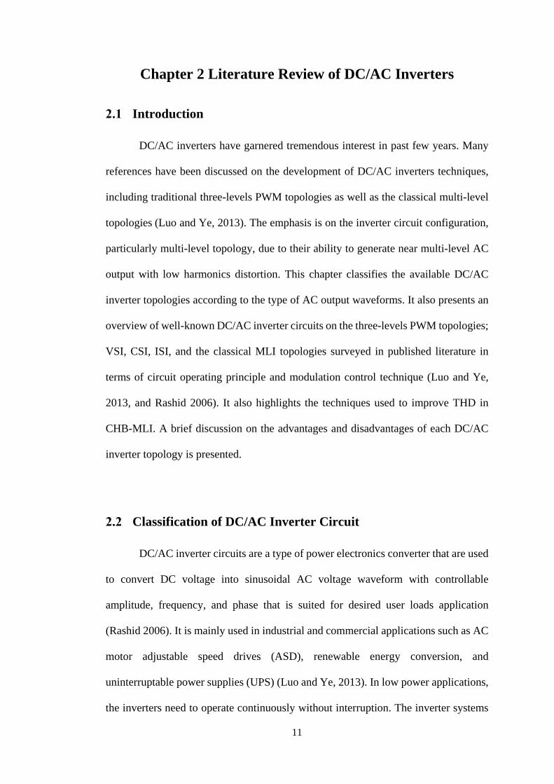
2.2.3 Impedance Source Inverter
Figure 2.4 shows three phases Impedance Source Inverter (ISI) (Anderson,
Peng 2008, Bao et al. 2011). This circuit topology is composed of seven power
semiconductor switches and a diode. Also, two inductors and two capacitors are
configured in an x-shaped impedance network. Sinusoidal Pulse Width Modulation
(SPWM) method is commonly used to obtain switching gate pattern so that to achieve
sinewave-modulated AC output voltage as shown in Figure 2.5(c). ISI has a unique
characteristic where it can become VSI if both inductors have zero inductance. On the
other hand, if both capacitors have zero capacitance, this ISI can become CSI. This
can provide buck-boost characteristics which are highly suitable for industrial
applications, such as distributed generation (DG) and variable speed drive (VSD).
Therefore, ISI has more flexibility in controlling AC output voltage than VSI and CSI.
The output voltage adjusted higher or lower than the DC source voltage or DC link
voltage. Traditional carrier-based Pulse Width Modulation (PWM) and Sinusoidal
Pulse Width Modulation (SPWM) can be used to control this inverter.
Two capacitors and inductors can provide protection from overvoltage and
overcurrent. This circuit is also robust from the shoot-through limitation which was
caused by EMI noise due to the existence of these two inductors and two capacitors
(Peng et al. 2013). Upper and lower bridge power switches controls can even operate
simultaneously in overlap time without shoot-through issues during a very short
period. Also, there is no need to set a short dead time control. The overall system cost
is low and efficiency is high because of fewer components.
The disadvantages of VSI, CSI, and ISI three-levels PWM inverters are:
• The power switches in both VSI, CSI, and ISI PWM inverters need to be

20
switched at high switching frequency PWM in order to achieve low distortion
in output voltage and current (Georgakas, Vovos & Vovos 2014, Carrasco et
al. 2006, Madouh, Ahmed & Al-Kandari 2012).
• Switching losses are high due to high switching frequency operation. The VSI
inverter is switched from a few kHz up to 100 kHz, while the CSI and ISI
inverters are switched at 20kHz up and above to achieve low harmonics output
distortion (Georgakas, Vovos & Vovos 2014 and Rozlan et al. 2015).
• The high switching frequency operation is useful in CSI, as smaller component
size can be used. However, this can lead to increase power dissipation in power
switch in both VSI and CSI inverter which also demand cooling systems (heat-
sink). This adds to inverter size and offsets the advantage of high switching
frequency operation.
• The output filter is required at both VSI and CSI inverter output can increase
system size and cost.
Figure 2.4 Three-Phase ISI Inverter

21
To achieve lower total harmonic distortion in output voltage and current
waveform, the power semiconductor switch in each of VSI, CSI, and ISI PWM inverter
circuits needs to operate at very high switching frequency i.e. 100 kHz. This high
switching frequency operation is associated with high switching losses in power
semiconductor switch which leads to reduce their efficiency when used in high power
applications.
Figure 2.5 DC/AC inverter output waveforms: (a) Three-levels voltage waveform using low-frequency square wave PWM modulation. (b) Three-levels voltage
waveform using unipolar high-frequency PWM modulation. (c) Sine-Modulated voltage waveform. (d) Seven-levels voltage waveform (multi-level)
(a)
(b)
(c)
(d)

22
Another inverter topology types called ‘multi-level inverter’ which can
generate a near AC (multi-level/staircase) output voltage with reduced harmonics
distortions and low power losses at the same time. This is explained in more detail in
the following section 2.2.4.

23
2.2.4 Classical Multi-Level Inverter Topologies
Multi-level DC/AC inverter topology is an alternative DC/AC inverter
configuration which is widely used in medium-voltage, high-power applications. It is
less popular in low-voltage, low-power applications, but preferred to traditional three-
levels PWM inverters (De, Banerjee, Gopakumar, Ramchand, & Patel, 2011). This
method is known for simultaneously generating fewer harmonics in output voltage and
current and smaller power losses. This technique also can overcome other problems of
the conventional two-level inverter as mentioned in the previous section.
The multi-level DC/AC inverter technique is different from the previous
conventional DC/AC inverter method, which vertically chops a reference sine voltage
waveform into several pulses width, horizontally chops a reference sine voltage
waveform into several pulses height, and synthesises these voltage levels to achieve
near sinusoidal multi-level or staircase output waveform at inverter output (Jiang, Lipo
1998). The m-level of the near sinusoidal multi-level or staircase output voltage is
usually synthesised from several lower DC voltage sources through low-voltage rated
switch controls at low switching frequency. Considering m is the number of output
phase voltage with respect to the negative terminal of the inverter. The harmonics
distortion in multi-level inverter output voltage and current can be reduced by
constructing a high number of levels or steps of inverter output voltage (Gupta et al.
2016). The higher the output voltage resolution, the closer to a sine waveform. This is
because a pure sine waveform has zero total harmonic distortion (Luo and Ye, 2013).
In achieving low harmonics output, the pulse width of the staircase waveform need to
control the by appropriate switching modulation method which can be categorised into
low-frequency modulation (Selective Harmonics Elimination, SHE) and high-

24
frequency modulation (Carrier-based PWM) (Luo and Ye, 2013, Arman, Darwish
2009). This refers to controlling the duration of the power switch to allow and block
voltage using low-voltage rated power semiconductor switches (i.e. IGBTs or Power
MOSFETs). The three main multi-level DC/AC converters have been reported in
literature (Arman, Darwish 2009, Luo and Ye, 2013, Gupta et al. 2016) which can be
referred as classical multi-level DC/AC inverter topology: Diode Clamped Multi-
Level Inverter (DC-MLI), Capacitor Clamped Multi-level Inverter (FC-MLI) and
Cascaded H-Bridge Multi-level Inverter (CHB-MLI). The following section describes
an overview of each circuit topology features, circuit operation, advantages, and
limitations.
2.2.4.1 Diode-Clamped Multi-Level Inverters
Diode-Clamped Multi-Level Inverters (DC-MLI) topology (Nabae, Takahashi
& Akagi 1981, De et al. 2011, Mecke 2011) has been used such in renewable energy
applications (Rashid 2006) where the PV is fed to input DC-link, as well as in
adjustable speed motor drives (Luo and Ye, 2013). The DC bus voltage is divided into
several voltage levels by several numbers of capacitors with a neutral point in the
middle. This creates several inner voltages levels at a different magnitude which are
clamped by either two extra diodes with different voltage ratings (Nabae, Takahashi
& Akagi 1981). These two diodes block the switch voltage to the half level of the DC
bus voltage. The near AC (multi-level/staircase) output voltage waveform is
synthesised from several inner voltage levels through several switches connected in
series which are controlled at the low-switching frequency. Figure 2.6 shows a three-
levels and five-levels DC-MLI circuit topologies. The number of output voltage levels
can also be extended from three-levels to five-levels or even more levels by adding

25
more power switches, capacitor and diodes components to generate a higher number
of output voltage levels. Therefore, its structure needs to be expanded. The multi-level
AC output voltage of DC-MLI (Va0) can be shaped by controlling the associated
power switches in appropriate switching pattern sequence as shown in Table 2.2 for 5-
level DC-MLI.
Advantages of DC-MLI circuit topology (Luo and Ye, 2013):
• For low fundamental switching frequency operation, small switching loss in
power switches due to low switch commutation. Therefore, the efficiency is
high.
• The DC link capacitors can be pre-charged as a group.
However, to obtain low output voltage harmonics, a number of output voltage
levels need to be increased. This requires a large number of power switches control
and clamp diode for blocking voltage, resulting in complex control circuits where each
switch is associated with a control gate drive unit (Luo and Ye, 2013). For higher
number of output voltage levels, the overall system can be bulky and expensive.

26
Figure 2.6 Diode-Clamped MLI circuit (a) Three-levels and (b) Five-levels
Table 2.2 Five-levels DC-MLI Switching States
DC bus voltage, (Vdc) Switch State
S1 S2 S3 S4 S5 S6 S7 S8
Va0 = 2Vdc 1 1 1 1 0 0 0 0
Va0 = 1Vdc 0 1 1 1 1 0 0 0
Va0 = 0 0 0 1 1 1 1 0 0
Va0 = −1Vdc 0 0 0 1 1 1 1 0
Va0 = −2Vdc 0 0 0 0 1 1 1 1
The generation of m-levels output voltage of DC-MLI inverter topology requires
several units of component device, such as:
• Number of power semiconductor switches = 2(m-1)
• Number of semiconductor diodes = 2(m-2)
• Number of DC-Link Capacitors = m-1
(a)
(b)

27
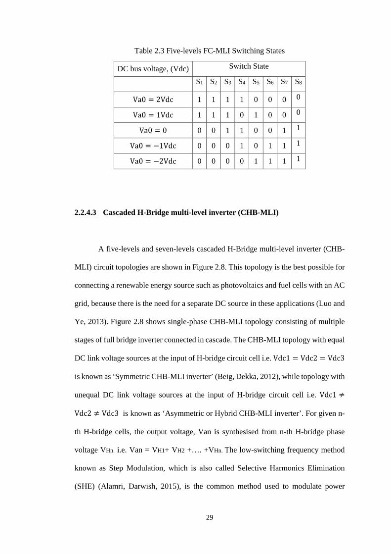
2.2.4.2 Flying-Capacitor Multi-Level Inverter
Figure 2.7 shows a Three-level and Five-level Flying-Capacitor Multi-Level
Inverter Flying-Capacitor Multi-Level Inverters circuit (Huang, Corzine 2004, He,
Cheng 2016). The DC bus voltage is divided into several voltage levels by several
numbers of capacitors with a neutral point in the middle. This creates several inner
voltages levels at a different magnitude which then are clamped using clamping
capacitors to one capacitor voltage levels. The multi-level or staircase AC voltage of
FC-MLI is synthesised from several inner voltage levels through several switches
connected in series. The conduction of the associated switches is controlled in
appropriate switching pattern at the low switching frequency. The five-levels output
voltages of FC-MLI and switching control pattern is shown in Table 2.3. The capacitor
C1 is charged when switches (S1) and (S3) are turned ON and discharged when (S2)
and (S3) are turned ON. The charge of C1 can be balanced by a proper selection of the
zero-level switch combination.
Advantages of FC-MLI circuit topology (Luo and Ye, 2013):
• The voltage synthesised in FC-MLI has more flexibility than a Diode Clamped-
MLI.
• A large number of clamping capacitors act like a capacitor bank which enables
the inverter to act as short backup supply for a short duration during a power
outage.
However, to obtain low output voltage harmonics, a number of output voltage levels
need to be increased. Therefore, its structure needs to be expanded (i.e. five-five levels
as shown in Figure 2.7 or more levels) to yield a higher number of output levels. This

28
requires a large number of power switches control and a bulk capacitor for clamping
voltage, resulting in complex control circuit where each switch is associated with a
control gate drive unit (Luo and Ye, 2013). For higher number of output voltage levels,
the overall system can be bulky and expensive.
The generation of m-levels output voltage of FC-MLI inverter topology requires
several units of component device, such as:
• Number of power semiconductor switches = 2(m-1)
• Number of clamping capacitors per phase = (m-1) x (m-2)/2
• Number of DC-link capacitors = m-1
Figure 2.7 Flying-Capacitor MLI circuit (a) Three-levels and (b) Five-levels
(a)
(b)
29
Table 2.3 Five-levels FC-MLI Switching States
DC bus voltage, (Vdc) Switch State
S1 S2 S3 S4 S5 S6 S7 S8
Va0 = 2Vdc 1 1 1 1 0 0 0 0
Va0 = 1Vdc 1 1 1 0 1 0 0 0
Va0 = 0 0 0 1 1 0 0 1 1
Va0 = −1Vdc 0 0 0 1 0 1 1 1
Va0 = −2Vdc 0 0 0 0 1 1 1 1
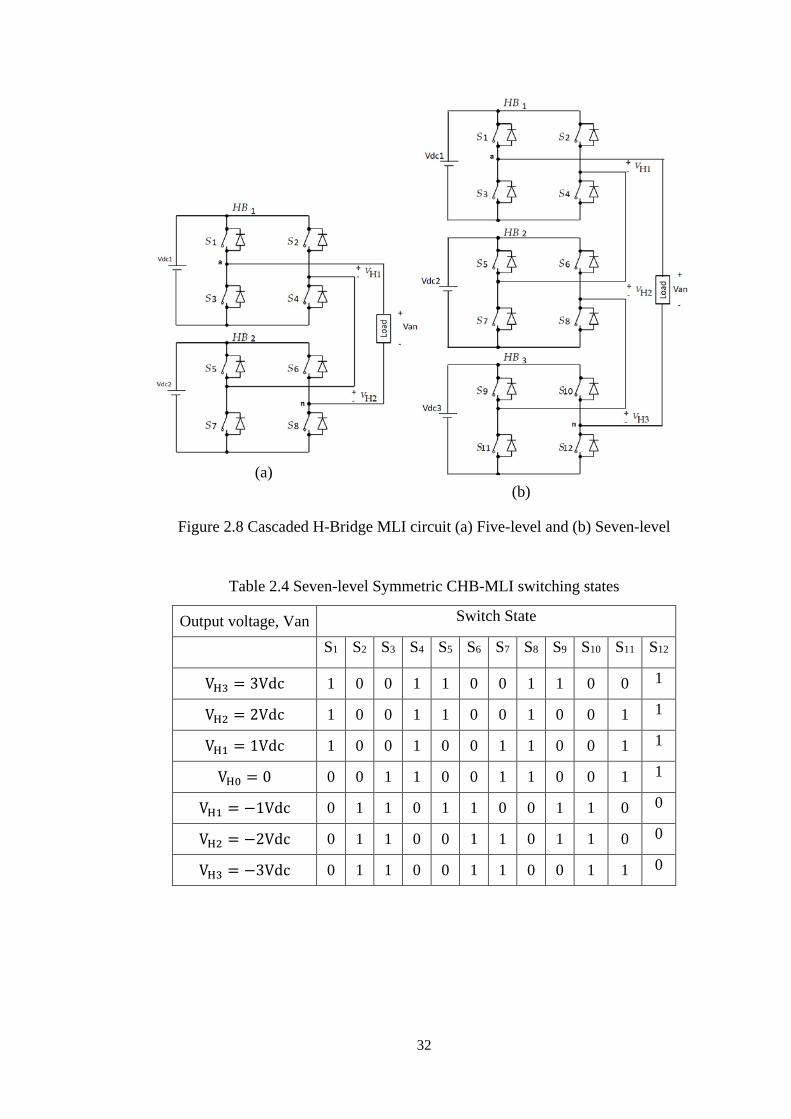
2.2.4.3 Cascaded H-Bridge multi-level inverter (CHB-MLI)
A five-levels and seven-levels cascaded H-Bridge multi-level inverter (CHB-
MLI) circuit topologies are shown in Figure 2.8. This topology is the best possible for
connecting a renewable energy source such as photovoltaics and fuel cells with an AC
grid, because there is the need for a separate DC source in these applications (Luo and
Ye, 2013). Figure 2.8 shows single-phase CHB-MLI topology consisting of multiple
stages of full bridge inverter connected in cascade. The CHB-MLI topology with equal
DC link voltage sources at the input of H-bridge circuit cell i.e. Vdc1 = Vdc2 = Vdc3
is known as ‘Symmetric CHB-MLI inverter’ (Beig, Dekka, 2012), while topology with
unequal DC link voltage sources at the input of H-bridge circuit cell i.e. Vdc1 ≠
Vdc2 ≠ Vdc3 is known as ‘Asymmetric or Hybrid CHB-MLI inverter’. For given n-
th H-bridge cells, the output voltage, Van is synthesised from n-th H-bridge phase
voltage VHn. i.e. Van = VH1+ VH2 +…. +VHn. The low-switching frequency method
known as Step Modulation, which is also called Selective Harmonics Elimination
(SHE) (Alamri, Darwish, 2015), is the common method used to modulate power

30
switches in Symmetric CHB-MLI. The seven-levels output voltage of CHB-MLI is
shown in Figures 2.9 and 2.10 and the switching control pattern is shown in Table 2.4.
This method allows several lower order harmonics to be eliminated while controlling
the amplitude of the fundamental output voltage.
Advantages of CHB-MLI circuit topology (Luo and Ye, 2013,):
- Low switching loss due to all power switches operating at the low switching
frequency.
- Low DC-link voltage means low rated-voltages power switch can be used (due
to low peak voltage flow through power switch). Hence, low dv/dt and less
electromagnetic interference (EMI).
Disadvantage of CHB-MLI circuit topology (Luo and Ye, 2013):
- Near sinusoidal output voltage with minimum THD can be achieved with a
large number of isolated DC-link sources, power switches, and diodes to
construct a high number of voltage levels.
In Hybrid or Asymmetric CHB-MLI inverter circuit topology, each DC link source of
H-bridge switches cell can have different DC link voltage values or different DC link
voltage integer ratio. It has hybrid modulation control which combines low and high-
frequency switching operation to modulate the low-voltage rated and high- voltage
rated power switches in Asymmetric/Hybrid CHB-MLI. The H-bridge power switch
circuit cell can be divided into a lower number of commutation cells (low-side H-
bridge cell) with high magnitude of DC link voltage sources and a higher number of
commutation cells (high-side H-bridge cell) with a lower magnitude of DC link voltage
sources. With an appropriate switching control pattern, a high number of output

31
voltage levels can be achieved with less number of power switches than symmetric
CHB-MLI.
Advantages of Asymmetric/Hybrid CHB-MLI circuit topology (Luo and Ye, 2013):
- The number of voltage level can be increased without needing an increasing
number of power switches. The higher number of levels gives higher output
resolution (where the resolution is referred to the step size of the staircase/
multi-level voltage) voltage, which is closer to a sine wave and low harmonics
output can be achieved.
- Different commutation operation of H-bridge switches circuit cell allows using
different types of power switches.
Disadvantage of Asymmetric/Hybrid CHB-MLI topology:
- Higher switching loss due to high-side power switches operating at high
switching frequency.
Therefore, the generation of m-levels output voltage of Symmetry CHB-MLI inverter
topology requires several units of component devices, such as:
• Number of power semiconductor switches = 2m-2
• Number of diodes = 2m-2
• Number of DC-link capacitors = (m-1)/2
32
Figure 2.8 Cascaded H-Bridge MLI circuit (a) Five-level and (b) Seven-level
Table 2.4 Seven-level Symmetric CHB-MLI switching states
Output voltage, Van Switch State
S1 S2 S3 S4 S5 S6 S7 S8 S9 S10 S11 S12
VH3 = 3Vdc 1 0 0 1 1 0 0 1 1 0 0 1
VH2 = 2Vdc 1 0 0 1 1 0 0 1 0 0 1 1
VH1 = 1Vdc 1 0 0 1 0 0 1 1 0 0 1 1
VH0 = 0 0 0 1 1 0 0 1 1 0 0 1 1
VH1 = −1Vdc 0 1 1 0 1 1 0 0 1 1 0 0
VH2 = −2Vdc 0 1 1 0 0 1 1 0 1 1 0 0
VH3 = −3Vdc 0 1 1 0 0 1 1 0 0 1 1 0
(a)(b)

33
Figure 2.9 Seven-level output voltage of the Symmetric CHB-MLI circuit
2.2.5 Improving THD in CHB-MLI circuit topology
The trend of recent development of multi-level DC/AC inverter is receiving
wider attention both in terms of topologies and modulation control technique (Gupta
et al. 2016). In CHB-MLI circuit topology, near sinusoidal staircase output voltage can
be generated from several low DC voltage levels. The higher number of voltage levels
in staircase waveform can result in better quality resolution of output waveform which
are close to a sinusoidal waveform. Hence, lower total harmonic distortion can be
achieved with the reduced size of the filter is required at the output. A pure AC
sinusoidal waveform has zero total harmonic distortion (Luo and Ye, 2013). The total

34
harmonic distortion in CHB–MLI can be improved by extending the number of output
voltage levels and also by DC link voltage levels and or switching angle optimisation
(Diong Sepahvand & Corzine 2013).
In order to track the sine waveform, the common method used to shape multi-
level or staircase AC voltage waveform of CHB-MLI circuit topology is done by
creating constant (equal step) voltage levels with respect to constant (equal step)
switching angle intervals (Luo and Ye, 2013). Figure 2.10 shows seven-levels near AC
output voltage waveform of the classical symmetric CHB-MLI circuit shown in Figure
2.8(b) with constant (equal step) DC link voltage with constant (equal interval) of
switching angle. The harmonics spectrum of the output voltage waveform contains
several higher lower order amplitudes (i.e.3rd, 5th, 7th and 9th) as shown in Figure 2.11.
These lower orders harmonics have led to the high total harmonic distortion in 7-levels
CHB-MLI output voltage.
Figure 2.10 Seven-levels output voltage of the Symmetry CHB-MLI circuit (Equal step DC link voltage)
-30
-20
-10
0
10
20
30
0 0.005 0.01 0.015 0.02 0.025 0.03 0.035 0.04
Out
put V
olta
ge V
an (
Vol
t)
Time (sec)
35
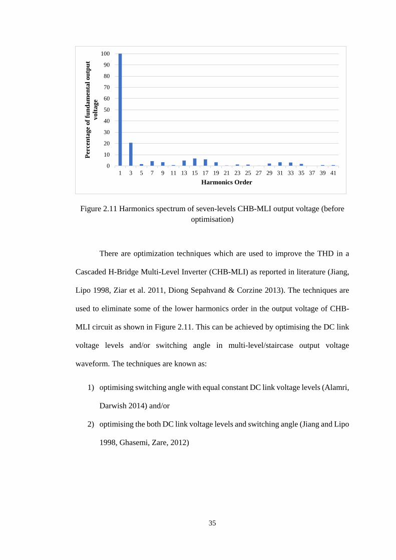
Figure 2.11 Harmonics spectrum of seven-levels CHB-MLI output voltage (before
optimisation)
There are optimization techniques which are used to improve the THD in a
Cascaded H-Bridge Multi-Level Inverter (CHB-MLI) as reported in literature (Jiang,
Lipo 1998, Ziar et al. 2011, Diong Sepahvand & Corzine 2013). The techniques are
used to eliminate some of the lower harmonics order in the output voltage of CHB-
MLI circuit as shown in Figure 2.11. This can be achieved by optimising the DC link
voltage levels and/or switching angle in multi-level/staircase output voltage
waveform. The techniques are known as:
1) optimising switching angle with equal constant DC link voltage levels (Alamri,
Darwish 2014) and/or
2) optimising the both DC link voltage levels and switching angle (Jiang and Lipo
1998, Ghasemi, Zare, 2012)
0
10
20
30
40
50
60
70
80
90
100
1 3 5 7 9 11 13 15 17 19 21 23 25 27 29 31 33 35 37 39 41
Perc
enta
ge o
f fun
dam
enta
l out
put
volta
ge
Harmonics Order

36
2.2.5.1 Optimising switching angle with equal constant DC link voltage levels
For seven-levels symmetric CHB-MLI, there are two numbers of harmonics
order can be eliminated in its output voltage spectrum (Alamri, Darwish 2014). To
eliminate these specific harmonic orders, the switching angle must be determined first.
The off-line calculation method called Selective Harmonics Elimination (SHE) is used
to determine switching angles that can eliminate specific or selected harmonics order
while controlling the magnitude of the fundamental voltage. The switching angle
calculation can be determined by iterative mathematical method (Alamri, Darwish,
2014). However, only two harmonics order can be eliminated (i.e. 5th and 7th orders)
(Alamri, Darwish, 2014).
2.2.5.2 Optimising both DC link voltage levels and switching angle.
Eliminating more harmonics content can be achieved by optimising both
voltage levels and switching angles as suggested in Jiang and Lipo 1998, Ghasemi,
Zare, 2012, so that the multi-level/staircase AC waveform can be shaped more closely
to sine waveform. This results in optimum DC link voltage steps and optimum
switching angles. By optimizing both DC link voltage levels and switching angle
technique, a near sinusoidal multi-level/staircase output voltage waveform is shaped.
The optimum DC link voltage ratio is found to be 1.4054 Vdc: 1.0543 Vdc: 0.56 Vdc
with 5th, 7th, 9th, 11th, 13th 15th and 17th harmonics orders eliminated as shown in
frequency spectrum Figure 2.13 (Ghasemi, Zare, 2012). The 3rd harmonic can be easily
eliminated in three-phase CHB-MLI inverter system configuration (Alamri, Darwish,
2014).

37
Figure 2.12 Optimised seven-levels CHB-MLI output voltage (Unequal step DC link
source)
For both optimisation cases (a) and (b), the Genetic Algorithm (GA) optimisation
method (Pandi, Devarajan, 2010) are used to solve the complicated non-linear
transcendental equation where the optimum angles can faster to converge than the
older Newton-Raphson Method. The GA optimisation tool in MATLAB was used for
this purpose.
Figure 2.13 Harmonics spectrum of seven-levels CHB-MLI (more harmonics order eliminated).
-40
-30
-20
-10
0
10
20
30
40
0 0.005 0.01 0.015 0.02 0.025 0.03 0.035 0.04
Out
put V
olta
ge V
an (V
olt)
Time (sec)
0102030405060708090
100
1 3 5 7 9 11 13 15 17 19 21 23 25 27 29 31 33 35 37 39 41 43
Perc
enta
ge o
f fun
dam
enta
l vo
ltage
Harmonics Order
38
The following section brief summarize the three-levels PWM inverter topologies and
the classical multi-level inverter topologies which explain and compare the advantages
and disadvantages of these two main DC/AC inverters as well as the improving THD
technique in the classical multi-level inverter topologies.
Summary of PWM Inverters & Multi-Level Inverter topologies
The main advantages of three-levels PWM inverter topologies for both PWM
and SPWM modulation operation that make its relevant in low power domestic
application and in high power industrial application such induction motor drives and
renewable energy system application are:
• Simple structure due to less number of component (i.e. power switches,
capacitor, inductor and diodes). The cost can be less.
• Simple control due to less number of power semiconductor switches used.
• Small size of passive components (i.e. capacitors and inductor) can be used
when operating at very high switching frequency.
• Reliable system due to less number of components used.
The main disadvantages of three-levels PWM inverter topologies for both PWM and
SPWM modulation operation are:
• Poor total harmonic distortion (THD)
• High switching losses in power semiconductor switches due to high
switching frequency operation.
• High dv/dt of output voltage and di/dt of output current can result in high
electromagnetic interference (EMI)
39
• Require of bulky and complex cooling system (heat-sink) can lead to bulky
overall system size
• Require heavy common modes and differential mode filters at output
• Low efficiency at higher switching frequency
In medium-voltage high-power application, the classical multi-level inverters
topologies are an attractive solution which much more preferred than three-levels
inverter due to many advantages such:
• Low total harmonic distortion (THD)
• Can be operated at low switching frequency
• Low switching loss
• Low dv/dt can result in low EMI
• Low voltage rating device can be used.
• High efficiency
The multi-level inverter topologies are not so popular in low power applications. For
low-power range, it can be preferred than three-levels PWM inverter topologies if the
power semiconductor switches used in PWM inverter circuit are operated at very high
frequency (i.e. >100 kHz).
Although classical multi-level topologies (DC-MLI, FC-MLI, and CHB-MLI) are
effective and can obtain minimum total harmonic distortion (THD). However, suffer
from some disadvantagous when to construct higher number of voltage levels of the
staircase/multi-level AC output waveform such:
• Require increasing number of power semiconductor switches, diodes and
capacitors as well as the number of isolated DC sources. This is due to the fact
that the multi-level inverter synthesized the higher output voltage levels from
40
several lower DC link voltages which are blocked/controlled by using several
low-rated rating power semiconductor switch devices. The higher number of
voltage levels means the lower the pulse height (DC linkage voltage). Lower
pulse height (and also the pulse width) can cause fewer of harmonics in output
spectrum which results in higher THD. The higher number of levels provides
higher voltage resolution (smaller voltage step size) in staircase AC output
voltage which can shape almost to the desired sinusoidal AC waveform.
• Although low-voltage rated of power semiconductor switches can be used
which can be operated at the low fundamental switching frequency, however
each switch requires gate driver control circuit, protection circuits, and cooling
units (heat sink).
• Higher numbers of output voltage levels can have complicated control circuit
and therefore the overall inverter system size can be bulky.
• The overall power losses in the inverter system can be high due to a large
number of power semiconductor switches used. This can degrade the overall
efficiency of the system (in transferring the real input power from source to the
load).
• Commutating the power semiconductor switches at low fundamental switching
frequency means the switches conduct in long conduction period so that allow
the DC link capacitor current discharging. However, this can increase the
conduction losses in the power switches and diodes.
• Inverter reliability can be decreased due to a large number of power switches
used.
• Overall inverter system size can be bulky in size and expensive in cost due to
many power switches used and associated control drive circuit.

41
In addition, the limitation of the optimization technique through Selective Harmonics
Elimination (SHE) method that is used to reduce the total THD of the output voltage
in the classical multi-level inverter (i.e. CHB-MLI) are:
• The need to undergo a complicated offline calculation of the transcendental
non-linear equation to determine the optimum switching angle and/or DC link
voltage that eliminates the specific lower harmonics orders.
• Only lower order harmonics order (which are located in the low-frequency
sideband of the output voltage frequency spectrum) can be selectively
eliminated by the optimum switching angle, while the passive output filter is
required to remove the higher order harmonics (which is located in the high-
frequency sideband of the output voltage frequency spectrum).
A summary of the above discussed inverter topologies, including three-levels
PWM inverter topologies and multi-level inverter topologies, showing the advantages
and disadvantages is presented. The selection of DC/AC inverter topologies depends
on the factors the designer must compromise such as power quality; the number of
levels and the total harmonics distortion (THD) of the AC output voltage and current,
size and volume and cost. From the literature review and the above summary, it has
been shown that the classical multi-level inverter topologies have a specific advantage
over three-levels PWM inverter in the point of view of low THD, low switching loss
and high efficiency. However, generating higher number of voltage levels using
classical multi-level inverter topologies for the sake of improving THD demands high
number of components (such as power switches, diodes and capacitors), complicated
control circuit, bulky in size and expensive. Hence, it is important to look at different
multi-level inverter topologies (newly-evolved) with reduced component count and

42
the current technologies that are used in designing inverter which have simple circuit
configuration, straightforward control operations, and less complex control circuits.
Summary
This chapter presents a review of power electronics DC/AC inverter circuits on
traditional three-levels PWM topologies and classical multi-level topologies surveyed
in published literature. It sets out the operating principles, modulation control
techniques, and harmonics elimination techniques. This chapter is important in
identifying the weaknesses and strengths of each of the identified DC/AC inverter
topologies. These points are very useful in providing a comparative study of available
DC/AC inverter topologies surveyed in published literature. It has been shown that the
classical multi-level inverters topologies have a specific advantage over conventional
three-levels PWM inverters type. Therefore, the research need to emphasise on multi-
level inverters topologies configuration type.
Over the last few years different multi-level inverter topologies/techniques
(switched-capacitor based) have evolved. Some of these techniques need to be fully
investigated in order to appreciate the proposed technique used in this thesis. Chapter
3 review some of the voltage boosting/varying techniques and their circuit topology
configurations. Some of these techniques also need to be fully investigated in order to
appreciate the selected technique used for the proposed inverter system. Also, critically
reviews some of these recent topologies and highlights the gaps and the challenges in
this field.

43
Chapter 3 Switched-Capacitor Circuit & Switched-Capacitor Multi-level DC/AC Inverter Topologies
Introduction
In Chapter 2, a general review of classical inverter type was presented. Over
the last five years, new types of inverter circuits have evolved from the classical
topologies (Luo and Ye, 2013, Gupta et al. 2016). Some of these techniques are
investigated in this chapter, as it covers the basics of the proposed inverter topology
presented in this thesis.
Many references have discussed the development of switched-capacitor circuit
(SCC) techniques which can be operated at high switching frequency (Darwish,
Mehta, 1990) and also operated at a hybrid switching frequency, which combines low
and high-frequency operation for many power electronics applications. Recent reviews
of published papers on DC/AC inverter topologies (Gupta et al. 2016) show the
tremendous interest of integrating SCC into DC/AC inverter to achieve output voltage
larger than the input voltage. The topic focuses on simple techniques and/or circuit
configurations (low number of switches, capacitors, diodes, and isolated DC sources),
which have the ability to boost and/or regulate/vary voltage.
In this chapter, an overview of voltage boosting/varying techniques is surveyed
in the literature. The available techniques (switched capacitors technique, magnetic
coupling, and multi-stage booster) are categorised. The available switched-capacitors
techniques are categorised according to their type of circuit topology/configuration
and connection. Some of these switched-capacitors techniques are investigated to
appreciate the proposed technique used in this thesis. A brief discussion on the

44
advantages and disadvantages of each voltage boosting/varying technique and each
type of switched-capacitor circuit’s topology/configurations and connections are
presented. A comparative study is conducted to help the author select an optimum
circuit topology/configuration (voltage regulator) to be implemented/applied in the
proposed inverter circuit (a new simple DC/AC inverter based switched capacitor
topology), which is conducted in Chapter 4.
Furthermore, critical review of the recent switched-capacitor multi-level
inverter topologies as reported in literature survey is also provided in this chapter. A
brief discussion of the advantages and disadvantages of each circuit topology is
presented. The gap and challenge in the recent multi-level DC/AC inverter based
switched-capacitor circuit topologies is identified.
Overview of Voltage Boosting Technique
Most renewable resources produce DC power sources, and inverters are used
to interface to the AC grid. A DC/DC converter or/and a transformer is combined at
DC or AC side in order to boost voltage to appropriate voltage levels. This is mainly
due to low input DC voltage obtained from most renewable energy sources, such as
domestic wind turbines, solar arrays, or fuel cells. In grid-connected inverter systems,
boosting output voltage is one of the challenges. There are numerous voltage boost
techniques with different circuit configurations that have been proposed in the
literature (Forouzesh et al. 2017). Voltage boost technique is defined as the ability of
circuit topology and technique to produce output voltage larger than the input voltage.
It involves voltage multiplication and/or voltage regulation/varying voltage processes
to the desired voltage levels. These processes are achieved by a combination of energy

45
storage elements (capacitors and inductors) and/or transformers in conjunction with
power semiconductor switches and diodes in specific topology and using a specific
technique. For the purpose of explaining the strength and weaknesses of each boosting
circuit topology/configuration, it is essential first to categorise the voltage boosting
techniques covered. Figure 3.1 shows the categorisation of the voltage boosting
technique.
Figure 3.1 Categorisation of voltage boosting technique
Three main techniques are included, namely switched capacitor, magnetic coupling,
and multi-stage booster. A review and investigation of the switched capacitor
technique is discussed in addition to other voltage boosting techniques (magnetic
coupling and multi-stage booster) conducted in literature. Upon this review and
investigation, the desired technique and/or circuit configuration is adopted showing
the justification of that selection. The following section discusses each of voltage
boosting techniques covered in this chapter.

46
Switched Capacitor
Switched Capacitor is the most famous voltage boosting technique. This
technique utilises energy storing elements such as capacitors and inductors in
conjunction with power semiconductor switches. These elements are combined in a
specific configuration to achieve high-voltage boost. The basic switched-capacitor (S-
C) circuit cell consists of power semiconductor switches and diodes with DC voltage
connected to input circuit. The most famous basic concept of S-C is known as charge
pump where pump energy is moved from one capacitor to another through appropriate
switching control technique. Its output voltage can reaches input voltage levels after
several sequences of switching control cycles. This has been successfully utilised for
power conversion in low power on chip DC-DC converter application.
Figure 3.2 Categorisation of switched capacitor according voltage gain/ ability and the type of circuit topology/configuration

47
The switched-capacitor circuit (SCC) technique can be classified according to
its voltage gain ability as well as its type of circuit topology/configuration connection
as shown in Figure 3.2. Using different circuit configuration and connection, this S-C
circuit can have low/medium-voltage gain or high-voltage gain. The low-voltage gain
S-C circuits have a simple structure due to it containing fewer component (switch and
capacitor) counts and simple control. Meanwhile, high-voltage gain S-C circuits have
a large overall circuit structure due to the multi-stages cell. This utilises more switches
and capacitor components. S-C has been applied for many other power electronic
applications, such DC/AC inverters (Luo and Ye, 2013) and AC power system such
active power filter and reactive power compensation (Darwish, Mehta, 1990, Arman,
Darwish, 2009, Arman, Marouchos & Darwish, 2012). The switched-capacitor circuit
(SCC) can also be classified according to the types of circuit topology/configuration
connections as shunt-connected SCC and series-parallel connection SCC.
Shunt-connected SCC topology has been used in many AC power system
applications. It is composed of capacitors, inductors, and power semiconductor
switches which are configured in shunt-connected configuration. This topology is
classified as low/medium-voltage gain/boost ability due to fewer numbers of
capacitors used in conjunction with power switches. For reactive power compensation,
it is incorporated with a thyristor in shunt-connected configuration to form Thyristor-
Switched Capacitors (TSC). It is used for controlling bus voltage and prevents voltage
collapse when high loading in AC power network systems is present (Mohan, 2002).

48
For active filter applications, this shunt-connected SCC technique has also
been presented in Darwish, Mehta, 1990, El-Habrouk, Darwish & Mehta 2000, Arman,
Darwish 2009 as a smoothly variable source of lagging and leading reactive power in
reactive AC power control applications (Darwish, Mehta, 1990, Arman, Darwish
2009). Some of the shunt-connected SCC circuit topologies with varying switch duty
cycle control technique were exhibits variable characteristic capabilities (Darwish,
Mehta & Thomson 1988). In addition, these techniques were found to be effective for
filtering harmonics applications such as automatically tuning impedance at any desired
harmonics to filter out (Arman, Darwish 2009, Arman, Marouchos & Darwish, 2012).
The available basic unit configurations of the shunt-connected SCC circuits are
shown in Figure 3.3 (a) Double Switch Single Capacitor (DSSC), (b) Double Switch
Double Capacitor (DSDC), (c) Single Switch Single Capacitor (SSSC) and (d) Triplen
Switch (Darwish, Mehta, 1990, Arman, Darwish 2009). A shunt-connected double
switch single capacitor (DSSC) SCC circuit configurations has shown it unique
variable capacitor features (Arman, Darwish 2009, Arman, Marouchos & Darwish,
2012). With an inductor is connected between AC voltage source and DSSC and/or
DSDC circuits input, variable capacitor behavior can be obtained by applying varying
switch duty cycle control technique in a specific switching pattern to the associated
switches. However, from another point of view, this behaviour can also lead to
providing varying voltage ability.

49
Figure 3.3 Basic configuration unit of the shunt-connected SCC
The following subsections review the operating principle of the shunt-
connected switched-capacitor circuit (SCC) topology. An investigation of the main
configuration of this topology is presented in addition to other configurations. This is
to identify the possibility of obtaining variable capacitor behaviour among topologies
with given DC source applied at the input that could provide voltage gain and/or
varying/regulating voltage ability. Upon examination, the optimum is accepted based
on its ability to comply with a strict set of criteria given as showing justification of that
selection. The main configuration is DSSC. An outline of other configurations includes
Single Switch Single Capacitor (SSSC), Double Switch Double Capacitor (DSDC),
and Triplen Switch.
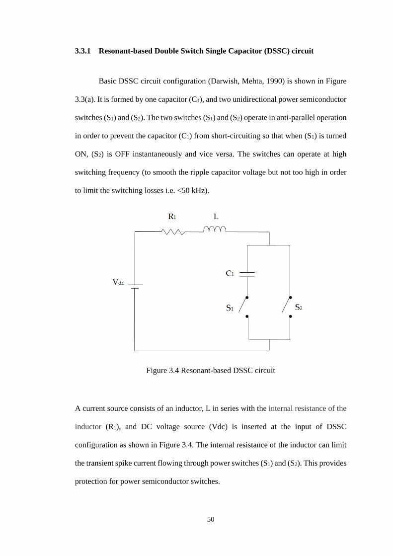
50
3.3.1 Resonant-based Double Switch Single Capacitor (DSSC) circuit
Basic DSSC circuit configuration (Darwish, Mehta, 1990) is shown in Figure
3.3(a). It is formed by one capacitor (C1), and two unidirectional power semiconductor
switches (S1) and (S2). The two switches (S1) and (S2) operate in anti-parallel operation
in order to prevent the capacitor (C1) from short-circuiting so that when (S1) is turned
ON, (S2) is OFF instantaneously and vice versa. The switches can operate at high
switching frequency (to smooth the ripple capacitor voltage but not too high in order
to limit the switching losses i.e. <50 kHz).
Figure 3.4 Resonant-based DSSC circuit
A current source consists of an inductor, L in series with the internal resistance of the
inductor (R1), and DC voltage source (Vdc) is inserted at the input of DSSC
configuration as shown in Figure 3.4. The internal resistance of the inductor can limit
the transient spike current flowing through power switches (S1) and (S2). This provides
protection for power semiconductor switches.

51
Due to switch anti-parallel operation, DSSC circuit branches are alternately connected
to the input DC supply. One branch forms a switched series resonance (R-L-C) circuit
which is connected in series with switch (S1) with resonant current flowing through it.
The other branch forms a series R-L circuit connected in series with a switch (S2) with
transient current flowing through it. Therefore, a combination of a current source and
DSSC configuration introduces a resonant-based DSSC circuit. This circuit
configuration has fewer switching components which can reduce the power loss. It is
composed of one capacitor (C1) and two semiconductor switches (S1) and (S2).
However, instantaneous switching control transition between on and off switch (S1 &
S2) states is required to avoid short-circuit problems which could occur for very short
period of time. This could lead to high surge current which can damage the switches.
Figure 3.5 DSSC circuit identical to the effective capacitance
The following subsections present two mathematical analyses for proving
purposes; switching function and transient analysis. The switching function analysis
is conducted to prove that a DSSC circuit with a varying switch duty cycle control
applied can introduce a variable capacitor. An inductor with its internal resistance is
connected in series with DC voltage at input provides a current source for a DSSC

52
circuit. The value of effective capacitance (Ceff) will be proven as it varies with
varying the duty cycle of the power switches where Ceff can be measured across
terminal (A’-B’) as shown in Figure 3.5.
3.3.1.1 Switching function Analysis of the resonant-based DSSC circuit
Switching function principle (Marouchos 2006) is the process of commutating
switches between turned on (1) and turned off (0) switch state in form of sequence of
pulses. The varying switch duty cycle controlled technique involves the computations
of power semiconductor switches (S1) and (S2) of the resonant-based DSSC SCC
circuit configuration at high switching frequency (>10 kHz). These switches are
operated in anti-parallel operation.
The resonant-based DSSC SCC circuit configuration is shown in Figure 3.5.
The circuit branches are alternately connected to the input DC supply. One branch
forms a switched series resonance (R-L-C) circuit which connected in series with
switch (S1) during its conduction period (𝐷𝐷𝑜𝑜= 1). The other branch form series (R-L)
circuit connected in series with switch (S2) during its conduction period (𝐷𝐷𝑜𝑜= 0). The
switch duty cycle 𝐷𝐷𝑜𝑜 can have any value between 0 and 1. Varying switch duty cycle
of the switches (𝐷𝐷𝑘𝑘) is the ratio of varying on-time switch duration 𝑡𝑡𝑜𝑜𝑛𝑛 over the entire
switch switching period 𝑇𝑇𝑠𝑠. The switching frequency of these switches can be
assigned as 𝑓𝑓𝑠𝑠.
The switching function can be expressed as:
𝐹𝐹(𝑡𝑡) = 𝐷𝐷𝑜𝑜 + (𝐴𝐴𝑛𝑛 cos(𝑛𝑛𝜔𝜔𝑠𝑠𝑡𝑡) + 𝐵𝐵𝑛𝑛 sin(𝑛𝑛𝜔𝜔𝑠𝑠𝑡𝑡))∞
𝑛𝑛=1
(3.1)

53
For the purpose of simplification, the switching instant is selected to be 𝑡𝑡1 =
−(𝑡𝑡𝑜𝑜𝑛𝑛 2⁄ ) which will simplify and reduced the previous equation to:
𝐹𝐹(𝑡𝑡) = 𝐷𝐷𝑜𝑜 + 2𝐾𝐾𝑛𝑛
∞
𝑛𝑛=1
cos(𝑛𝑛𝜔𝜔𝑠𝑠𝑡𝑡)
(3.2)
where high switching period is 𝑇𝑇𝑠𝑠 = 1/𝑓𝑓𝑠𝑠 and the angular switching frequency 𝜔𝜔𝑠𝑠 =
2𝜋𝜋𝐹𝐹𝑠𝑠 and 𝐾𝐾𝑛𝑛 = sin𝑛𝑛 𝜋𝜋 𝐷𝐷𝑜𝑜/2 . Let,
∅(𝑡𝑡) = 2𝐾𝐾𝑛𝑛
∞
𝑛𝑛=1
cos(𝑛𝑛𝜔𝜔𝑠𝑠𝑡𝑡)
(3.3)
Hence,
𝐹𝐹(𝑡𝑡) = 𝐷𝐷𝑜𝑜 + ∅(𝑡𝑡)
(3.4)
where 𝐹𝐹(𝑡𝑡) is the switching function of switch (S1). The switching function of (S2)
will be the complementary of (S1), 𝐹𝐹′(𝑡𝑡),
𝐹𝐹′(𝑡𝑡) = 1 − 𝐹𝐹(𝑡𝑡)
(3.5)
The voltage across points A’- B’ (DSSC SCC circuit branch as shown in Figure 3.5),
is given by:
𝑉𝑉𝑑𝑑𝑐𝑐 = 𝑅𝑅1𝑖𝑖 + 𝐿𝐿𝑑𝑑𝑖𝑖𝑑𝑑𝑡𝑡
+ 𝑉𝑉𝐴𝐴’− 𝐵𝐵’
(3.6)
𝑉𝑉𝑑𝑑𝑐𝑐 = 𝑅𝑅1𝑖𝑖 + 𝐿𝐿𝑑𝑑𝑖𝑖𝑑𝑑𝑡𝑡
+ 𝐹𝐹(𝑡𝑡). 𝑣𝑣𝑐𝑐(𝑡𝑡) (3.7)

54
where,
𝑣𝑣𝑐𝑐(𝑡𝑡) =1𝐶𝐶1 𝐹𝐹(𝑡𝑡) 𝑖𝑖(𝑡𝑡) 𝑑𝑑𝑡𝑡 𝑡𝑡
0
(3.8)
𝑣𝑣𝑐𝑐(𝑡𝑡) =1𝐶𝐶1 𝐷𝐷𝑜𝑜 . 𝑖𝑖(𝑡𝑡)𝑑𝑑𝑡𝑡 +
1𝐶𝐶1
𝑡𝑡
0 ∅(𝑡𝑡). 𝑖𝑖(𝑡𝑡)𝑡𝑡
0𝑑𝑑𝑡𝑡
(3.9)
Assuming the circuit is underdamped (𝛼𝛼 < 𝜔𝜔0). The instantaneous current during
Mode 1 is
𝑖𝑖1(𝑡𝑡) =𝑉𝑉𝑑𝑑𝑐𝑐𝜔𝜔𝑟𝑟𝐿𝐿
𝑒𝑒−𝛼𝛼𝑡𝑡 sin(𝜔𝜔𝑟𝑟𝑡𝑡)
(3.10)
where the damping factor,
𝛼𝛼 = 𝑅𝑅12𝐿𝐿
(3.11)
and the resonant frequency,
ω0 = 1
𝐿𝐿𝐶𝐶1
(3.12)
and the ringing frequency (or damped resonant frequency),
𝜔𝜔𝑟𝑟 =124𝐿𝐿 − 𝐶𝐶1𝑅𝑅12
𝐶𝐶1𝐿𝐿2
(3.13)
Consider only fundamental component frequency. So, 𝐹𝐹(𝑡𝑡) = 𝐷𝐷𝑜𝑜
𝑣𝑣𝑐𝑐(𝑡𝑡) =1𝐶𝐶1 𝐷𝐷𝑘𝑘 . 𝑖𝑖1(𝑡𝑡) 𝑑𝑑𝑡𝑡 𝑡𝑡
0=𝐷𝐷𝑜𝑜𝐶𝐶1𝑉𝑉𝑑𝑑𝑐𝑐𝜔𝜔𝑟𝑟𝐿𝐿
𝑒𝑒−𝛼𝛼𝑡𝑡 sin(𝜔𝜔𝑟𝑟𝑡𝑡)
(3.14)

55
Hence, the capacitor voltage is
𝑣𝑣𝑐𝑐(𝑡𝑡) = −𝐷𝐷𝑜𝑜𝑉𝑉𝑑𝑑𝑐𝑐𝜔𝜔𝑟𝑟𝐶𝐶1
𝑒𝑒−𝛼𝛼𝑡𝑡 (α sin(𝜔𝜔𝑟𝑟𝑡𝑡) + 𝜔𝜔𝑟𝑟 cos(𝜔𝜔𝑟𝑟𝑡𝑡))
(3.15)
The voltage across terminal point A’- B’,
𝑉𝑉𝑥𝑥𝑥𝑥 = 𝐹𝐹(𝑡𝑡). 𝑣𝑣𝑐𝑐(𝑡𝑡) (3.16)
𝑉𝑉𝑥𝑥𝑥𝑥 = [𝐷𝐷𝑜𝑜 + ∅(𝑡𝑡)] −𝐷𝐷𝑜𝑜𝑉𝑉𝑑𝑑𝑐𝑐𝜔𝜔𝑟𝑟𝐶𝐶1
𝑒𝑒−𝛼𝛼𝑡𝑡 (α sin(𝜔𝜔𝑟𝑟𝑡𝑡) + 𝜔𝜔𝑟𝑟 cos(𝜔𝜔𝑟𝑟𝑡𝑡))
(3.17)
𝑉𝑉𝑥𝑥𝑥𝑥 = 𝐷𝐷𝑜𝑜2 1
𝜔𝜔𝑟𝑟𝐶𝐶1 [−𝑉𝑉𝑑𝑑𝑐𝑐 𝑒𝑒−𝛼𝛼𝑡𝑡 (α sin(𝜔𝜔𝑟𝑟𝑡𝑡) + 𝜔𝜔𝑟𝑟 cos(𝜔𝜔𝑟𝑟𝑡𝑡))]
(3.18)
Let,
𝐼𝐼 = −𝑉𝑉𝑑𝑑𝑐𝑐 𝑒𝑒−𝛼𝛼𝑡𝑡 (α sin(𝜔𝜔𝑟𝑟𝑡𝑡) + 𝜔𝜔𝑟𝑟 cos(𝜔𝜔𝑟𝑟𝑡𝑡))
(3.19)
Hence,
𝑉𝑉𝑥𝑥𝑥𝑥 = 𝐷𝐷𝑜𝑜2 [𝑋𝑋𝑐𝑐] 𝐼𝐼
(3.20)
Since the effective capacitance (between terminal point A’-B’ as shown in Figure
3.5) is given by:
𝑋𝑋𝑐𝑐𝑐𝑐𝑓𝑓𝑓𝑓 =𝑉𝑉𝐴𝐴’− 𝐵𝐵’
𝐼𝐼
(3.21)
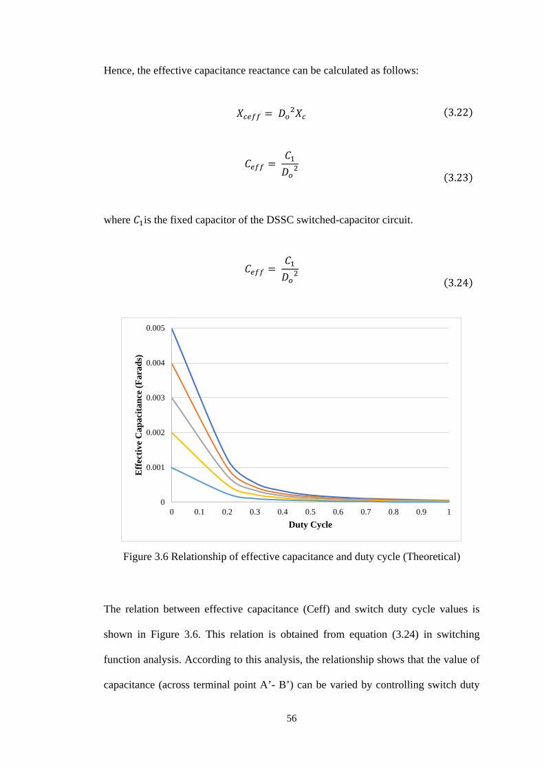
56
Hence, the effective capacitance reactance can be calculated as follows:
𝑋𝑋𝑐𝑐𝑐𝑐𝑓𝑓𝑓𝑓 = 𝐷𝐷𝑜𝑜2𝑋𝑋𝑐𝑐
(3.22)
𝐶𝐶𝑐𝑐𝑓𝑓𝑓𝑓 = 𝐶𝐶1𝐷𝐷𝑜𝑜2
(3.23)
where 𝐶𝐶1is the fixed capacitor of the DSSC switched-capacitor circuit.
𝐶𝐶𝑐𝑐𝑓𝑓𝑓𝑓 = 𝐶𝐶1𝐷𝐷𝑜𝑜2
(3.24)
Figure 3.6 Relationship of effective capacitance and duty cycle (Theoretical)
The relation between effective capacitance (Ceff) and switch duty cycle values is
shown in Figure 3.6. This relation is obtained from equation (3.24) in switching
function analysis. According to this analysis, the relationship shows that the value of
capacitance (across terminal point A’- B’) can be varied by controlling switch duty
0
0.001
0.002
0.003
0.004
0.005
0 0.1 0.2 0.3 0.4 0.5 0.6 0.7 0.8 0.9 1
Eff
ectiv
e C
apac
itanc
e (F
arad
s)
Duty Cycle
57
cycle values (between 𝐷𝐷𝑜𝑜=0 and 𝐷𝐷𝑜𝑜=1) of the associated switch (S1) (and its
complement switch (S2)). At 𝐷𝐷𝑜𝑜=1, the capacitor branch is disconnected from the
DSSC circuit as shown in Figure 3.5 and hence the circuit has zero capacitance. At
𝐷𝐷𝑜𝑜=0, the capacitor is connected to the circuit and the circuit has a fixed capacitor.
Given a current source at input and varying switch duty cycle values control technique,
which makes it clear that DSSC circuit configuration shows a variable capacitor
behavior due to resonant frequency. By substituting C1 with Ceff in equation (3.30),
this behavior can lead to varying voltage ability.
3.3.1.2 DC Transient Analysis
The resonant-based DSSC circuit with a varying switch duty cycle controlled
has also been analysed using DC transient analysis (voltage - current characteristic).
This is to investigate its ability to vary or regulate voltage. The voltage across the
capacitor (C1) will be proven that it varies with varying switch duty cycle values. Due
to anti-parallel switch operation, the DSSC circuit branches are alternately connected
to the input DC supply via a current limiter (an inductor (L) in series with its internal
resistance (R1)). This forms two modes of operations. During first mode (Mode 1), a
switched series resonance (R-L-C) circuit connection is formed on the left DSSC
circuit branch, as shown in Figure 3.7. A current limiter is connected in series with a
fixed capacitor (C1) to be controlled by a switch (S1). The resonant current flowing
through it and capacitor (C1) is charging f or duration 𝑡𝑡𝑎𝑎. During the second mode
(Mode 2), series (R-L) circuit connection is formed on the other branch where a current
limiter is connected in series with switch (S2). The transient current flows through
switch S2 and the capacitor is disconnected (holds its initial charge).

58
Figure 3.7 Resonant-based DSSC circuit in Mode 1
For simplification, the analysis is made during capacitor (C1) charging Mode 1
(Switch (S1) is closed and (S2) is open) as shown in Figure 3.7. Varying switch duty
cycle control means varying on-time duration 𝑡𝑡𝑎𝑎 of the associated switches. Assuming
this circuit operates in continuous conduction mode (CCM), the inductor current never
reach zero at every beginning of the capacitor charging interval.
Using Kirchhoff's Voltage Law (KVLs), the equation can be written as
𝑅𝑅1𝑖𝑖𝐿𝐿1(𝑡𝑡) + 𝐿𝐿𝑑𝑑𝑖𝑖𝐿𝐿1(𝑡𝑡)𝑑𝑑𝑡𝑡
+ 1𝐶𝐶1 𝑖𝑖𝑐𝑐1 𝑑𝑑𝑡𝑡 + 𝑣𝑣𝑐𝑐(𝑡𝑡 = 0) = 𝑉𝑉𝑠𝑠
(3.25)
Assuming the circuit is underdamped (𝛼𝛼 < 𝜔𝜔0). The instantaneous current during
Mode 1 is
𝑖𝑖(𝑡𝑡) = 𝑖𝑖𝐿𝐿1(𝑡𝑡) = 𝑖𝑖𝑐𝑐1(𝑡𝑡) = 𝑉𝑉𝑠𝑠 − 𝑉𝑉𝑐𝑐0𝜔𝜔𝑟𝑟𝐿𝐿
𝑒𝑒−𝛼𝛼𝑡𝑡 sin(𝜔𝜔𝑟𝑟𝑡𝑡)
(3.26)

59
where the instantaneous charging current is equal to inductor current and capacitor
current i.e. 𝑖𝑖(𝑡𝑡) = 𝑖𝑖𝐿𝐿1(𝑡𝑡) = 𝑖𝑖𝑐𝑐1(𝑡𝑡). Assuming the initial condition of inductor current
is zero i.e. 𝑖𝑖𝐿𝐿(𝑡𝑡 = 0) = 0 and the initial capacitor voltage is 𝑉𝑉𝑜𝑜 i.e. 𝑣𝑣𝑐𝑐(𝑡𝑡 = 0) = 𝑉𝑉𝑐𝑐0.
where the damping factor,
𝛼𝛼 = 𝑅𝑅12𝐿𝐿
(3.27)
and the resonant frequency,
ω0 = 1
𝐿𝐿𝐶𝐶1
(3.28)
and the ringing frequency (or damped resonant frequency),
𝜔𝜔𝑟𝑟 =124𝐿𝐿 − 𝐶𝐶1𝑅𝑅12
𝐶𝐶1𝐿𝐿2
(3.29)
the peak-to-peak ripple voltage across fixed capacitor (C1) can be expressed as
Δ𝑣𝑣𝑐𝑐 = 𝑣𝑣𝑐𝑐(𝑡𝑡) − 𝑣𝑣(𝑡𝑡 = 0) =1𝐶𝐶1 𝑖𝑖(𝑡𝑡) 𝑑𝑑𝑡𝑡 𝑡𝑡
0
(3.30)
Or capacitor ripple voltage can also be expressed as
Δ𝑣𝑣𝑐𝑐 = 𝑣𝑣𝑐𝑐(𝑡𝑡) − 𝑉𝑉𝑐𝑐0 = −𝑉𝑉𝑠𝑠 − 𝑉𝑉𝑐𝑐0 𝑒𝑒−𝛼𝛼(𝑡𝑡 ) α𝜔𝜔𝑟𝑟
sin𝜔𝜔𝑟𝑟(𝑡𝑡 ) −
cos𝜔𝜔𝑟𝑟(𝑡𝑡)
(3.31)
The capacitor voltage equation during Mode 1
𝑣𝑣𝑐𝑐(𝑡𝑡) = −𝑉𝑉𝑠𝑠 − 𝑉𝑉𝑐𝑐0 𝑒𝑒−𝛼𝛼(𝑡𝑡 ) α𝜔𝜔𝑟𝑟
sin𝜔𝜔𝑟𝑟(𝑡𝑡 ) − cos𝜔𝜔𝑟𝑟(𝑡𝑡) + 𝑉𝑉𝑐𝑐0
(3.32)

60
where 𝑣𝑣𝑐𝑐(𝑡𝑡) is the peak capacitor voltage, 𝑣𝑣(𝑡𝑡 = 0) = 𝑉𝑉𝑐𝑐0 is the initial capacitor
voltage and 𝑖𝑖(𝑡𝑡) is the instantaneous charging current.
Figure 3.8 and Figure 3.9 illustrates the peak capacitor voltage and peak capacitor
current during Mode 1. This shows the characteristics of complete capacitor charge
interchange. At initial start-up, this capacitor voltage and capacitor current oscillates
and exponentially decreases amplitude under transient conditions. Once the steady-
state condition is reached, the capacitor voltage is equal to DC input voltage (Vdc).
The capacitor current becomes resonant-type (sinusoidal).
Figure 3.8 Capacitor voltage during Mode 1 (Theoretical)
0
10
20
30
40
50
60
70
80
90
100
0.0E+00 2.0E-04 4.0E-04 6.0E-04 8.0E-04 1.0E-03
Vol
tage
(Vol
t)
Time (sec)
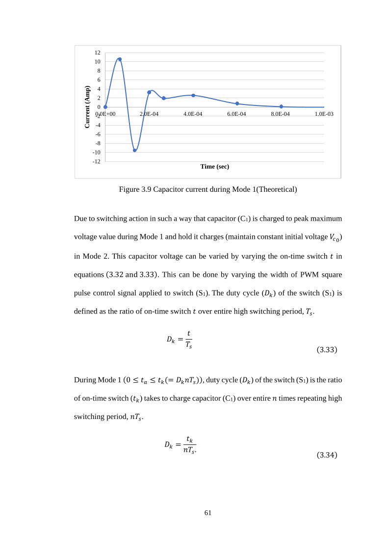
61
Figure 3.9 Capacitor current during Mode 1(Theoretical)
Due to switching action in such a way that capacitor (C1) is charged to peak maximum
voltage value during Mode 1 and hold it charges (maintain constant initial voltage 𝑉𝑉𝑐𝑐0)
in Mode 2. This capacitor voltage can be varied by varying the on-time switch 𝑡𝑡 in
equations (3.32 and 3.33). This can be done by varying the width of PWM square
pulse control signal applied to switch (S1). The duty cycle (𝐷𝐷𝑘𝑘) of the switch (S1) is
defined as the ratio of on-time switch 𝑡𝑡 over entire high switching period, 𝑇𝑇𝑠𝑠.
𝐷𝐷𝑘𝑘 =𝑡𝑡𝑇𝑇𝑠𝑠
(3.33)
During Mode 1 (0 ≤ 𝑡𝑡𝑎𝑎 ≤ 𝑡𝑡𝑘𝑘(= 𝐷𝐷𝑘𝑘𝑛𝑛𝑇𝑇𝑠𝑠)), duty cycle (𝐷𝐷𝑘𝑘) of the switch (S1) is the ratio
of on-time switch (𝑡𝑡𝑘𝑘) takes to charge capacitor (C1) over entire 𝑛𝑛 times repeating high
switching period, 𝑛𝑛𝑇𝑇𝑠𝑠.
𝐷𝐷𝑘𝑘 =𝑡𝑡𝑘𝑘𝑛𝑛𝑇𝑇𝑠𝑠.
(3.34)
-12-10-8-6-4-202468
1012
0.0E+00 2.0E-04 4.0E-04 6.0E-04 8.0E-04 1.0E-03
Cur
rent
(Am
p)
Time (sec)

62
The longer charging duration time 𝑡𝑡𝑘𝑘 = 𝐷𝐷𝑘𝑘𝑛𝑛𝑇𝑇𝑠𝑠; the more charge can be stored and
hence, the larger the capacitor voltage (𝑣𝑣𝑐𝑐(𝑡𝑡)).
Δ𝑣𝑣𝑐𝑐 = 𝑣𝑣𝑐𝑐(𝑡𝑡𝑘𝑘) − 𝑣𝑣(𝑡𝑡 = 0) =1𝐶𝐶1 𝑖𝑖(𝑡𝑡) 𝑑𝑑𝑡𝑡 𝑡𝑡𝑘𝑘
0
(3.35)
With 𝑛𝑛 times repeating switching period, 𝑛𝑛𝑇𝑇𝑠𝑠 of the PWM pulses signal applied to the
associated switches causes the voltage across point X-Y to fluctuate from zero to
maximum (peak capacitor voltage) creating large ripple voltage. In this case, low
capacitance (C1) (i.e. 1uF or 10uF) can be used in achieving a large range of voltage
across point X-Y (peak capacitor voltage). Therefore, the maximum peak amplitude
of the staircase/multi-level output voltage can be determined by the value of capacitor
chosen.
If k-th duty cycle value (𝐷𝐷𝑘𝑘) applied with increasing time point 𝑡𝑡𝑘𝑘 can yield k-th
capacitor voltage level (𝑣𝑣𝑐𝑐𝑘𝑘(𝑡𝑡𝑘𝑘)) which can also be denoted as the voltage increment.
Δ𝑣𝑣𝑐𝑐𝑘𝑘 = 𝑣𝑣𝑐𝑐(𝐷𝐷𝑘𝑘𝑛𝑛𝑇𝑇𝑠𝑠) − 𝑣𝑣(𝑡𝑡 = 0) =1𝐶𝐶1 𝑖𝑖(𝑡𝑡) 𝑑𝑑𝑡𝑡 𝑡𝑡𝑘𝑘
0
(3.36)
𝑣𝑣𝑐𝑐𝑘𝑘(𝑡𝑡𝑘𝑘) = −𝑉𝑉𝑠𝑠 − 𝑉𝑉𝑐𝑐0 𝑒𝑒−𝛼𝛼(𝑡𝑡𝑘𝑘 ) α𝜔𝜔𝑟𝑟
sin𝜔𝜔𝑟𝑟(𝑡𝑡𝑘𝑘) − cos𝜔𝜔𝑟𝑟(𝑡𝑡𝑘𝑘) + 𝑉𝑉𝑐𝑐0
(3.37)
Hence, the relation between 𝑘𝑘-th capacitor voltage level (𝑣𝑣𝑐𝑐𝑘𝑘(𝑡𝑡𝑘𝑘)) and duty cycle (𝐷𝐷𝑘𝑘)
within appropriate switching time interval 0 ≤ 𝐷𝐷𝑘𝑘 ≤ 𝑡𝑡𝑘𝑘(= 𝐷𝐷𝑘𝑘𝑛𝑛𝑇𝑇𝑠𝑠) where 𝑘𝑘 =
1,2, …𝑁𝑁) and 𝑁𝑁 = 𝑚𝑚−12
(𝑘𝑘 is the number of steps and 𝑚𝑚 is the number of levels peak
to peak output voltage) can be described by the following expression.

63
𝑣𝑣𝑐𝑐𝑘𝑘(𝐷𝐷𝑘𝑘 ) =
⎩⎪⎨
⎪⎧𝑣𝑣𝑐𝑐1(𝐷𝐷1),
.
.
.
.𝑣𝑣𝑐𝑐𝑁𝑁(𝐷𝐷𝑁𝑁),
0 ≤ 𝐷𝐷1 ≤ 𝑡𝑡1 ....
𝑡𝑡𝑁𝑁−1 ≤ 𝐷𝐷𝑁𝑁 ≤ 𝑡𝑡𝑁𝑁
(3.38)
The following Figure 3.10 and Table 3.1 shows the relationship between capacitor
voltage level or voltage increment and duty cycle. This illustrates the characteristic of
the resonant-based DSSC switched-capacitor circuit with a switch duty cycle
controlled technique, where the voltage across the fixed capacitor (C1) can be varied
by controlling or varying the duty cycle value.
Figure 3.10 Relationship between capacitor voltage and duty cycle with respect to S1 for DSSC SCC circuit (Theoretical)
0
10
20
30
40
50
60
0 0.1 0.2 0.3 0.4 0.5 0.6 0.7 0.8 0.9 1
Vol
tage
(Vol
t)
Duty Cycle

64
Table 3.1 Relationship between capacitor voltage level & duty cycle (Theoretical Calculation)
k Duty Cycle
Value
𝐷𝐷𝑘𝑘
Capacitor
voltage level
𝑣𝑣𝑐𝑐𝑘𝑘(𝐷𝐷𝑘𝑘) (Volt)
0 1 0
1 0.95 6.8
2 0.85 18.3
3 0.75 27.8
4 0.65 34.9
5 0.55 40.0
6 0.4 44.8
7 0.3 46.9
8 0.2 48.5
9 0 50
As the duty cycle value of the switches is decreased, the magnitude of capacitor
voltage level increase. According to this behaviour, this resonant-based DSSC circuit
with switch duty cycle controlled technique has the ability to vary voltage across the
capacitor (C1) due to resonant. The capacitor voltage level can be varied by controlling
the duty cycle value of the switch S1. The characteristic of this circuit configuration
showed that it behaves like a voltage regulator. This can be considered as a new
technique of regulating/varying voltage which can lead to producing multi-level
voltage. Besides having voltage gain and/or varying voltage ability, it also contains
low component count (one inductor ((where R1 represents an internal resistance of the
inductor)), one capacitor, and two power semiconductor switches). An inductor with
it internal resistance at input circuit can limit the spike/transient current flowing
through power semiconductor switches. Due to this exhibited behaviour and low

65
component count, therefore the resonant-based DSSC circuit with varying switch duty
cycle controlled technique will be used to implement a new optimum inverter
topology, which is the aim of this research. This new technique is for the purpose of
obtaining rectified multi-level or staircase voltage waveform in the first conversion
stage of the proposed inverter by setting specific switching timing control to the
associated switches.
3.3.2 Resonant-based Double Switch Double Capacitor (DSDC) circuit
Basic DSDC circuit configuration (Darwish, Mehta, 1990) is shown in Figure
3.3(b). It is composed of two capacitors (C1 and C2) and two semiconductor switches
(S1) and (S2). These switches can be operated in the anti-parallel manner with a varying
switch duty cycle controlled so that when (S1) is closed, (S2) is open instantaneously
and vice versa. With a current source is applied at input, a resonant-based Double
Switch Double Capacitor (DSDC) circuit is formed as shown in Figure 3.11.
Figure 3.11 Resonant shunt-connected DSDC SCC circuit
By adopting the same approach used in DSSC circuit analysis, the voltage equation
for DSDC SCC circuit can be written as follows:

66
During Mode 1, the voltage equation for C1 branch
𝑅𝑅1𝑖𝑖𝐿𝐿1(𝑡𝑡) + 𝐿𝐿𝑑𝑑𝑖𝑖𝐿𝐿1(𝑡𝑡)𝑑𝑑𝑡𝑡
+ 𝑣𝑣𝑐𝑐1 = 𝑉𝑉𝑠𝑠 (3.39)
During Mode 2, the voltage equation for C2 branch
𝑅𝑅1𝑖𝑖𝐿𝐿1(𝑡𝑡) + 𝐿𝐿𝑑𝑑𝑖𝑖𝐿𝐿1(𝑡𝑡)𝑑𝑑𝑡𝑡
+ 𝑣𝑣𝑐𝑐2 = 𝑉𝑉𝑠𝑠 (3.40)
The following Figure 3.12 shows the relationship between capacitor voltage level or
voltage increment and duty cycle for DSDC circuit. This illustrates the characteristic
of the resonant-based DSDC switched-capacitor circuit with switch duty cycle
controlled technique. Each capacitor in DSDC circuit branch is alternately charged,
repeating switching action such as continuously chopping the voltage across
capacitors. This has no effect on varying capacitor voltage. Therefore, this can be
concluded that the DSDC circuit topology does not have varying voltage ability. It also
contains many components (two capacitors and two switches). More switches add
power losses in the circuit.
Figure 3.12 Relationship between capacitor voltage and duty cycle with respect to S1 (Theoretical)
0
10
20
30
40
50
60
0 0.1 0.2 0.3 0.4 0.5 0.6 0.7 0.8 0.9 1
Vol
tage
(Vol
t)
Duty Cycle
67
3.3.3 Resonant-based Single Switch Single Capacitor (SSSC) circuit.
Basic SSSC circuit configuration (Darwish, Mehta, 1990) is shown in Figure
3.3(c). This is the simplest circuit configuration in shunt-connected switched-capacitor
circuit topology. This circuit consists of single unidirectional switch (S1) connected in
parallel with single fixed capacitor (C). This combination is connected to the input of
a current source which forms the resonant-based Single Switch Single Capacitor
(SSSC) circuit as shown in Figure 3.13.
Figure 3.13 Resonant-based Single Switch Single Capacitor circuit
It has simple control operations due to few components used. Only a single switch is
switched on and off at single switching frequency operation. Due to this operation, the
branch is alternately connected to the input of a current source. One branch forms a
series resonance (R-L-C) circuit during first half switching cycle of Switch (S1).
During the other half switching cycle, the circuit forms series (R-L) circuit. However,
this can have short-circuited problems if the switch is turned while the voltage across
capacitor (C1) is not zero. In practice, the switch can only be closed when the voltage
68
across capacitors is very small (at least), which is close to zero, otherwise it will short-
circuit the capacitor. Given that a current source at the input and varying switch duty
cycle is controlled, a Single Switch Single Capacitor (SSSC) circuit configuration is
unable to provide varying voltage behaviour.
3.3.4 Resonant-based Triplen switch SCC circuit
The resonant shunt-connected Triplen switch circuit is shown in Figure 3.14.
A basic triplen switch configuration is shown in Figure 3.3(d). It is formed by a double
switch single capacitor DSSC circuit with third switch branch connected in parallel.
The third branch consists of a unidirectional switch in series with a resistor (R2).
Figure 3.14 Resonant shunt-connected Triplen switch circuit
Introducing this auxiliary branch is to avoid a short-circuit condition during switching
transition (between on and off) of anti-parallel switch operations, which was noticed
in previous DSSC and DSDC circuits’ operations. This is because the power
semiconductor switching devices take a finite time to change from one state to another.
During this transition action between (S1) and (S2), there is a very short period where

69
both switches are closed, leading to short-circuiting the capacitor (C1), and the
switches are subjected to destructive surge current. The resistor (R2) in the third branch
provides smooth transfer of current from one branch to another. The introduction of
an additional switch branch in this circuit topology provides short-circuit protection
for the switches from a dangerous surge current during the transition. Its operation and
characteristics are quite similar to DSSC circuit but in this case the third modes (dead
period mode) must be included. By adopting the same approach used in DSSC circuit
analysis, the voltage equation for Triplen SCC.
During Mode 1, the voltage equation for C1 and S1 branch as follows:
𝑅𝑅1𝑖𝑖𝐿𝐿1(𝑡𝑡) + 𝐿𝐿𝑑𝑑𝑖𝑖𝐿𝐿1(𝑡𝑡)𝑑𝑑𝑡𝑡
+ 𝑣𝑣𝑐𝑐1 = 𝑉𝑉𝑠𝑠 (3.41)
During Mode 2, the voltage equation for S2 branch as follows:
𝑉𝑉𝑠𝑠 = 𝑖𝑖𝐿𝐿2(𝑡𝑡)𝑅𝑅1 + 𝐿𝐿𝑑𝑑𝑖𝑖𝐿𝐿2(𝑡𝑡)𝑑𝑑𝑡𝑡
(3.42)
During Mode 3, the voltage equation for S3 branch as follows:
𝑉𝑉𝑠𝑠 = 𝑖𝑖𝐿𝐿3(𝑡𝑡)(𝑅𝑅1 + 𝑅𝑅2) + 𝐿𝐿𝑑𝑑𝑖𝑖𝐿𝐿3(𝑡𝑡)𝑑𝑑𝑡𝑡
(3.43)
Given a current source at the input and varying switch duty cycle control., this
circuit has varying voltage ability. The following Figure 3.15 shows the relationship
between capacitor voltage and duty cycle. As the duty cycle value of the switches is
decreased, the magnitude of capacitor voltage level increase. The capacitor voltage
level can be varied by controlling the duty cycle value of the switch S1. The
characteristic of triple switch circuit configuration showed that it behaves like a
voltage regulator. However, the operation is associated with complicated controls and

70
adds more components. The small resistance (R2) in series switch could be associated
with high power dissipation, which could degrade the efficiency of transferring power
from the input source to load. The additional switch could introduce more switching
losses when operating at high switching frequency (the switch introduces losses due
to their intrinsic characteristic of switching at high frequency).
Figure 3.15 Relationship between capacitor voltage and duty cycle with respect to S1 for Triplen SCC circuit (Theoretical)
3.3.5 Capacitor-based switched-capacitor circuit in series-parallel connection
The series-parallel connection is other types of circuit connection used in the
switched-capacitor technique. The switched-capacitor (S-C) circuit cells can be
configured in series-parallel connection so that they (S-C cells) can perform energy
transfer from one to another to obtain voltage multiplication. These cells can be
expanded to multi-stages to generate higher voltage level/gain. The basic cell is
composed of power semiconductor switches, diodes and capacitors as shown in Figure
3.16. This circuit configuration can be considered as a capacitor-based switched-
0
10
20
30
40
50
60
0 0.1 0.2 0.3 0.4 0.5 0.6 0.7 0.8 0.9 1
Vol
tage
(Vol
t)
Duty Cycle

71
capacitor circuit (Luo and Ye, 2013). This has been used in DC/DC converter to
accomplish energy transfer and voltage conversion.
Figure 3.16 Basic unit of S-C cell
Figure 3.17 SC cell operation: (a) Capacitor Charging and (b) Capacitor discharging
Figure 3.16 shows a basic unit of switched-capacitor circuit cell (Luo and Ye,
2013). The switches Si and P connect a capacitor C in series and parallel with DC
voltage. The switches Si and P have a complementary operation which means when
switch Si is switched on, switch P must be switched off and vice versa. Otherwise,
short-circuiting occurs across DC voltage. Figures 3.17(a) and (b) shows the operation
mode of the basic unit of the switched-capacitor circuit. When switch P is switched on
during the first half of the switching cycle, the capacitor C is charged to DC voltage
i.e. Va = Vi = Vdc via conducting diode, Di. During the second half of the switching
cycle, Switch Si is switched on and capacitor start to discharge. The diode Di becomes
reverse-biased to prevent back discharging to DC voltage source. The DC voltage
source is connected in series with the charged capacitor C, and therefore these voltages

72
can be added i.e. Va = Vdc + Vi while the capacitor C current flows to the load. To
achieve a higher number of voltage levels (multi-level voltage), multiple stages of S-
C circuit must be connected in cascaded. Series-parallel S-C circuit topologies are
popular owing to their structure modularity and capability for bulk integration. Small
capacitor size can be used with high switching frequency operations. They utilise
capacitors efficiently without having a magnetic element. Hence, no issues related to
magnetic, such as electromagnetic interference (EMI), are problems.
However, this type of S-C has high transient current (also known as spike
current) which can degrade power density and efficiency. For high power levels (high
power applications), spike current waveform is exhibited among capacitors. In
addition, multiple stages of S-C circuit are required to achieve high-voltage gain. This
demands a large number of power switches, diodes, and capacitors. In synthesising the
output voltage, unbalance capacitor voltage problem can occur when more than one
capacitor is connected in series. High switching frequency operation can diminish this
problem. Yet, this can lower the converter efficiency due to increased switching losses
across power switches. The large numbers of power switches used also adds to the
power losses.

73
Other Voltage Boosting Techniques
The other types of voltage boosting techniques are also briefly discussed. These
techniques include magnetic coupling and multi-stage booster. The presentation of
these techniques aims to justify the selection of the circuit topology/technique to be
adopted for the new proposed inverter system.
3.4.1 Magnetic Coupling
Magnetic coupling is one of well-known voltage boost method which is used
in isolated and non-isolated DC/DC converters. Transformer-based boost (Forouzesh
et al. 2017) is popular among the voltage boosting techniques due to flexibility in boost
voltage ability. It has been used in DC/DC converters for long to accomplish voltage
boosting by turns ratio or/and to provide isolation protection between low-level
voltage side and high-level voltage side. This transformer can be added at the DC or
AC side of the power electronics converters. In high-power (>10 kW) wind energy
system application, traditional full-bridge buck inverters (Xue et al. 2004) are used
with line frequency transformers as shown in Figure 3.18. These line frequency
transformers are used to step-up voltage and provide galvanic isolation. However, they
are bulky in size, heavy in weight, and costly due to the heavy magnetic core (the
bulkiest component in transformer) to sustain high power.

74
Figure 3.18 Buck Inverter with bulky line-frequency transformer
3.4.2 Multi-Stage Booster
Multi-stage booster, also known as multi-level, technique is gaining attention
to achieve higher output voltage using multiple stage cells. The cells contain capacitors
and diodes (as blocking voltage) in conjunction with power switches (as blocking
voltage) which are configured in modular stack structures. This technique has been
implemented in DC/DC Multi-Level Boost converters for high power DC supply
(Rosas-Caro et al. 2010) as shown in Figure 3.19. In renewable energy system
applications, multiple DC sources are obtained from distributed energy sources
(batteries, photovoltaics, and fuel cells). These sources are fed into numbers of H-
bridge cells in cascaded (modular) multi-level DC/AC topology order to synthesise
higher number of AC output voltage levels. The modular structure can ease
maintenance and save time such in replacement/swap of the faulty module.

75
Figure 3.19 DC/DC Multi-Level Boost Converter
High-power density can be achieved by simply adding more cells. High output voltage
can be obtained efficiently without transformer at output. However, this requires a
large number of components (power switches, diodes, and capacitors) which increases
the system size (as it is bulky) and cost.
The following section presents a comparative study of different voltage boosting
techniques, as well as different SCC topologies/techniques covered in this thesis. This
leads to the selection of an optimum topology/technique to be applied in the proposed
inverter system
General Comparison of Voltage Boosting Techniques
It is apparent from the preceding review of voltage boosting techniques
(switched capacitor, magnetic coupling, and multi-stage booster) that high-voltage
gain and/or varying voltage can be achieved by using the step-up converter circuits.

76
The step-up converter (switched capacitor, transformer-based, and multi-level) circuits
are used to implement these techniques in many DC/DC converters. Each of these
circuits has their own advantages and disadvantages. Table 3.2 shows a general
comparison of the discussed voltage boosting techniques, showing the advantages and
disadvantages according to the type of circuit topology/configuration and connection.
The selection of the boosting technique to be applied for the proposed inverter depends
on factors such voltage boost/gain and varying voltage ability, low component use
(power switches, diodes, and capacitors), switching frequency, and capability for
integration. The literature review and the general comparison of the boosting
techniques show that the switched-capacitor circuit (SCC) technique has a specific
advantage over the others. This is due to the fact that it has a cell-based structure which
is easy to integrate into various circuit structure and high-voltage gain/step up ability.
Therefore, the SCC technique is given special attention in this chapter.
Selection of the SCC for the Proposed Inverter
It is apparent from the preceding comparison that the switched-Capacitor
Circuit (SCC) technique is superior to the others. This SCC is classified according to
the type of circuit topologies/configurations and connections. Two major SCC
topologies/techniques covered in literature, namely capacitor-based SCC (in series-
parallel connection) and resonant-based SCC (in shunt connection) configurations,
were reviewed and investigated.
These topology/techniques need to be carefully chosen before they can be
integrated into the proposed inverter system leading to the introduction of a new
inverter topology. This is to ensure minimum shortcomings in the overall proposed

77
inverter system performance. The selected SCC topology/technique configuration
should satisfy the following criteria:
1. Voltage gain/boost ability and/or varying/regulating voltage technique;
2. Low component count (power switches, diodes, and capacitors);
3. Ability to operate at high switching frequency; and
4. Capability of integration (circuit cell easy to be integrated into various circuits).
The aim of the multiple-stage inverters system is to have boost voltage/varying
voltage and/or isolation carried out in the first circuit stage and inversion in the second
stage (Xue et al. 2004). However, this system is bulky due to many voltage multiplier
cells and/or transformers.
The selected SCC topologies/techniques of the new proposed optimum inverter
topology should provide voltage boost and/or varying/regulating voltage technique
ability in order to step up the low-voltage at the input. This can diminish the
requirement of huge multiple stages of cells for voltage multiplication or bulky and
heavy transformers for a step-up voltage. The voltage boost and/or varying voltage
ability technique is required to step up the low input voltage and/or to produce different
magnitude voltage levels (multi-level).
The selected technique should have low component count (power switches,
capacitors, and diodes). This is to reduce the overall system structure and control
complexity. The reduction of the number of power switches can lead to reducing the
switching losses which helps to reduce overall power losses in the proposed inverter
system.

78
Table 3.2 General comparison among voltage boosting techniques
Voltage Boosting
Techniques
Type of circuit
topology/configuration and
connection
Advantages Disadvantages
Switched-
Capacitor Circuit
(SCC)
Capacitor-based SCC in series-
parallel connection
- high-voltage gain
- can operate without
inductors (capacitor-
based)
- can be integrated to other
structure
- high spike current at initial start-up can
increase switching losses and decrease
system efficiency
- high components (power switches,
diodes and capacitors) due to huge
multiple stages of cells
Resonant-based SCC (with
inductor) in shunt connection
- low or medium-voltage
gain.
- Low component use
- can limit the spike
current
- can be integrated to other
structure
- need more passive components
(capacitors and inductors)
- sensitive to internal resistance of the
inductor
Magnetic
Coupling
Transformer-based - the high-voltage boost - effect of leakage inductance such as a
large voltage spike

79
- flexible in boost ability
due to changeable turn
ratio
- bulky and costly due to the heavy
magnetic core to sustain high power
Multi-stage
Booster
Multi-level - high power density
- modular structure
- can be integrated to other
structures
- large number of components
- heavy bulky and costly

80
Also, the selected technique should be able to operate at high switching
frequency PWM operation to smooth the voltage waveform (which is high enough i.e.
<50 kHz to limit the switching losses across power switches), and a small size
capacitor and inductor can be used. This high switching frequency PWM can cause the
PWM control pulse to narrow so that to smooth (narrow ripple) the voltage waveform.
In the frequency spectrum of the voltage, the lower order harmonics content (located
in the lower frequency side band) can be suppressed to a higher frequency side band.
This higher order harmonics content could be easily filtered by small output filter size
at the proposed inverter output.
Finally, the selected SCC topologies/technique should have a structure that can
easy to be integrated into various circuit structures. The trade-off is between harmonics
in voltage and switching losses, and switching losses which must be compromised.
These sets of criteria are important for the author in deciding the adopted optimum
switched-capacitor circuit.
Table 3.3 illustrates a comparison between SCC topologies/techniques in terms
of the performance criteria and fair comment set. This was a guideline for the author
to decide an optimum SCC topology/technique to be integrated into the proposed
inverter circuit. The attractive SCC topologies/techniques configurations are found to
be; capacitor-based (series-parallel connection) circuits, resonant-based DSSC, and
resonant-based triplen switch circuits. These configurations are capable of producing
varying voltage with switch duty cycle controlled and/or multi-level voltage.
Capacitor-based can achieve high-voltage gain by employing multiple stages of S-C
cells. It can be operated without an inductor (as inductors are large and heavy
compared with other components in the circuit).
81
However, it has the drawback of high transient current (or spike current) which
can lead to high losses across power switches and degrade the system efficiency.
Meanwhile, resonant-based SCC (with inductor) in shunt connection topology has the
advantage of limiting this spike current by the internal resistance of the inductor. This
can decrease the switching losses across semiconductor switches as well as provide
high surge current protection for switches in this topology.
Both capacitor-based and resonant-based triplen switch configurations contain
more components which can increase switching losses. Despite many components and
complex control, the triplen switch configuration can avoid the short-circuiting
problem by the third auxiliary branch (a resistor in series with a power switch).
However, high power dissipation in the auxiliary resistor. Meanwhile, resonant-based
DSSC configuration with varying switch duty cycle control can perform
varying/regulating voltage ability. This new technique evolved after conducting the
investigation above. An investigation has been conducted through mathematical
transient analysis. This can be considered as a new technique of varying voltage using
switched capacitor technique. This circuit configuration has a low power switch count.
The power losses could be less. The associated high switching frequency operation
allows using small passive component sizes.
Therefore, this comparative study directed the author to select resonant-based
SCC DSSC as the optimum technique. This technique aimed to produce rectified sine
(staircase/multi-level) voltage waveform in the first stage of the proposed inverter
design. The proposed inverter will be applied in low power applications (i.e. aircraft
and marine applications). The formation of this waveform is explained in detail in
Chapter 4.

82
Table 3.3 Comparison between SCC topologies/techniques for the performance selection criteria
Topology Circuit
configuration/connection
Criteria Comment
Capacitor-
based
switched-
capacitor
circuit
Series-parallel connection
- high-voltage gain / voltage
multiplication ability
- can operate without inductors (as
inductors are bulky and heavy
compared with other
components in the circuit)
- modular structure which can be
integrated into various structure
- Suitable to generate high multi-level
voltage for high power application by
adding stage of S-C cells, but this needs
large number of components and huge
circuit layout
- high power loss (switching losses) due to
a large number of power switches which
are required
- high transient current (spike current) in the
capacitor can degrade system efficiency
Resonant-
based
switched-
Double Switch Double
Capacitor (DSSC)
- varying/regulating voltage
technique (showing ability to
vary voltage with a varying duty
cycle controlled)
- need to be operated at high
switching frequency (FS > 5 kHz)
- needs five components
- spike current is limited
- suitable for varying voltage
- high switching losses
- medium component count

83
capacitor
circuit
- can be integrated into various
structures
Double Switch Double
Capacitor (DSDC)
- needs six components
- can be integrated into various
structures
- spike current is limited
- not showing varying/regulating voltage
- high switching losses
- medium component count
Single Switch Single
Capacitor (SSSC)
- not showing varying/regulating
voltage
- needs four components
- can be integrated into various
structures
- spike current is limited
- not suitable for varying voltage due to
short-circuited problem
- low switching losses
- low component count
Triplen Switch Circuit - able to vary voltage with a duty
cycle controlled
- needs to be operated at high
switching frequency (FS > 5 kHz)
- needs seven or eight components
- can be integrated into various
structures
- spike current is limited
- suitable for varying voltage
- high power dissipation and switching
losses
- high component count
- complex control

84
The following section presents critical reviews some of the recent switched-
capacitor multi-level inverter topologies as reported in literature survey. A brief
discussion is presented on the advantages and disadvantages of each circuit topology.
It also highlights the gaps and the challenges required in this field.
Switched-Capacitor Multi-Level DC/AC Inverter Topologies
Producing an acceptable sinusoidal output voltage waveform and boosting the
output voltage are two challenges (Rahim et al. 2011) in DC/AC inverters. The
transformer can be used to accomplish voltage step-up and/or provide isolation.
However, this increases the size and cost of the inverter. The efficiency of the inverter
system can decrease due to the bulky magnetic element.
Over, the last few years another family group of multi-level DC/AC inverter
topologies/techniques have evolved which are known as switched-capacitor multi-
level inverter topologies. These topologies/techniques contain components (capacitors
and power semiconductor switches) arranged in a specific configuration. The
switching control can be fundamental low-frequency modulation or high-frequency
carrier-based pulse-width modulation (PWM). They can generate a high number of
AC output voltage levels (high-voltage gain) from single DC input source using less
number of power semiconductor switches and isolated DC source usage than the
classical multi-level inverter circuits (Gupta et al. 2016). They have simple circuit
configuration (due to low power semiconductor switch count), straightforward control
operations, and less complex control circuits (Luo and Ye, 2013, Gupta et al. 2016).
They have been used in renewable energy sources and industrial applications (Luo and
Ye, 2013).
85
These new evolved multi-level DC/AC inverter topologies accomplish two-
stage power conversion. The first stage comprises of Switched-Capacitor Circuit
(SCC) which is used to boost DC input voltage to the desired voltage levels (voltage
appears across a series of capacitors). The associated power switches are controlled in
such a way that rectified sine multi-level/staircase waveform is shaped during the
positive cycle of AC output. The second stage is H-bridge circuit which changes the
polarity of magnitude output voltage between positive and negative and vice versa.
These topologies have a voltage boosting feature; the low input voltage can be step-up
to produce higher AC output voltage levels.
There are numerous switched-capacitor multi-level inverter topologies with
different SCC configurations that have been proposed in the literature (Luo and Ye,
2013, Gupta et al. 2016). For the purpose of explaining the strengths and weaknesses
of each circuit topology, it is essential first to categorise the circuit topology covered.
Figure 3.20 shows the categorisation of the switched-capacitor multi-level inverter
topologies. These topologies can be classified according to the component/element
used as; resonant-based (with inductor) SCC, and capacitor-based (without inductor)
SCC surveyed in published literature. For resonant-based SCC, three configuration
type are included namely; Cascaded Boost-Switched-Capacitor Multi-Level Inverter
(CBSC-MLI), Switched-Capacitor Boost Multi-level Inverter Using Partial Charging
(SCM-MLI), and Switched-Inductor Multi-Level Inverter (SI-MLI). For capacitor-
based SCC, two configuration types are included namely; Switched-Capacitor inverter
using Series/Parallel Conversion (SCI-S/P), and Hybrid Multi-level Inverter using
Switched-Capacitor unit (HSC-MLI).

86
Figure 3.20 Classification of switched-capacitor multi-level inverter topologies
The following sections review different circuit configurations of the switched-
capacitor multi-level inverter topologies covered in this chapter. This shows the merits
and limitation of each technique.
3.7.1 Cascaded-Boost Switched-Capacitor Multi-Level Inverter
Figure 3.21 shows five-levels output voltage of Single-phase Cascaded Boost-
Switched-Capacitor Multi-Level Inverter (CBSC-MLI) circuit topology (Axelrod,
Berkovich and Ioinovici 2005). It is two-stage inverter which is formed by switched-
capacitor boost converter and conventional H-bridge circuit. The switched-capacitor
(S-C) boost circuit stage composes of the switched-capacitor unit, diodes, and an
inductor element. The DC input voltage can be stepped up to obtain multi-level DC

87
voltage waveform by adding multiple stages of switched-capacitor (S-C). The control
switches are operated at a fundamental low-frequency (fundamental low-frequency
modulation method). The multi-level voltage is applied to the input of full H-bridge
inverter to generate staircase AC voltage waveform without a transformer at output
load. It has the advantage that the input voltage can be stepped up to achieve higher
output voltage without demanding multiple separate DC sources at input. This
topology inverter suffers from fundamental low-frequency operating of the control
switch. Low harmonics can be achieved by increasing number of output voltage levels.
This consequently requires a large number of switch and capacitor components that
act as voltage gain in this case.
Figure 3.21 Five-levels Cascaded Boost-Switched-Capacitor Multi-Level Inverter
circuit topology

88
3.7.2 Switched-Capacitor Boost-Multi-Level Inverter Using Partial Charging
Figure 3.22 shows Single-Phase Switched-Capacitor Boost-Multi-level
Inverter Using Partial Charging (SCB-MLI) circuit topology that generates 13-levels
multi-level output voltage through partial capacitor charging technique (Chan and
Chau 2007). It is formed by a two-stage circuit, switched-capacitor (S-C) boost, and
full H-bridge.
Figure 3.22 Thirteen-levels Switched-Capacitor Boost-Multi-Level inverter circuit topology
This topology has similar features to previous inverter topology which was
proposed by Axelrod, Berkovich and Ioinovici (2005) where the low input DC voltage
can be stepped up to produce higher staircase AC output voltage without requiring a
number of isolated DC sources. The multi-level output voltage and the frequency
spectrum of output voltage; five, seven and thirteen-levels, as shown in Figure 2.23 to
2.27 can be obtained by using switched-capacitor (S-C) boost circuit operating in
partial charging technique. The switched-capacitor (S-C) boost circuit is controlled by
applying specific switching pulse pattern to switches controlling capacitors. The

89
partial charging works in such a way that each capacitor is step-by-step charged to
three different voltage levels. The voltage levels can have an equal step (Vc1 = Vc2 =
Vc3) or unequal step (Vc1 ≠ Vc2 ≠ Vc3). A higher number of voltage levels can be
achieved by adding a number of capacitors with its associated control switches. The
capacitor may act as voltage gain. The partial charging technique may realise multi-
level voltage step per capacitor. This may in turn reduce the number of switches and
component count usage. However, to obtain low harmonics in output voltage, the
number of voltage levels need to be increased, which demands a large number of
capacitors and switch components to be used. This may cause the overall system to be
highly expensive, bulky, complex controlled, and less reliable due to many switch and
capacitor usages.
Figure 23 Five-levels output voltage of the SCB-MLI circuit
-25
-20
-15
-10
-5
0
5
10
15
20
25
0 0.005 0.01 0.015 0.02 0.025 0.03 0.035 0.04
Out
put V
olta
ge (V
olt)
Time (Sec)

90
Figure 3.24 Harmonics spectrum of five-levels SCB-MLI output voltage
Figure 3.25 Seven-levels output voltage of the SCB-MLI circuit
0
10
20
30
40
50
60
70
80
90
100
1 3 5 7 9 11 13 15 17 19 21 23 25 27 29 31 33 35 37 39 41
Perc
enta
ge o
f fun
dam
enta
l out
put v
olta
ge
Harmonics Order
-30
-20
-10
0
10
20
30
0 0.005 0.01 0.015 0.02 0.025 0.03 0.035 0.04
Out
put V
olta
ge (V
olt)
Time (Sec)

91
Figure 3.26 Harmonics spectrum of seven-levels SCB-MLI output voltage
Figure 3.27 Thirteen-levels output voltage of the SCB-MLI circuit
-50
-40
-30
-20
-10
0
10
20
30
40
50
0 0.005 0.01 0.015 0.02 0.025 0.03 0.035 0.04
Out
put V
olta
ge (V
olt)
Time (Sec)
0
10
20
30
40
50
60
70
80
90
100
1 3 5 7 9 11 13 15 17 19 21 23 25 27 29 31 33 35 37 39 41
Perc
enta
ge o
f fun
dam
enta
l out
put v
olta
ge
Harmonics Order

92
Figure 3.28 Harmonics spectrum of thirteen-levels SCB-MLI output voltage
3.7.3 Switched-Inductor Multi-Level Inverter
Switched-Inductor Multi-Level Inverter (SI-MLI) topology has been proposed
by Luo and Ye (2013). Figure 3.29 shows the single-phase seven-levels SI-MLI circuit
and Figure 3.30 and 3.31 shows staircase output voltage waveform and the frequency
spectrum of output voltage respectively. It consists of two-stage circuits which are
connected in cascade. The first stage is a combined conventional boost DC/DC
converter and switched-capacitor (S-C) circuit and the second stage is an H-bridge
circuit. The conventional boost DC/DC is used to boost the low input voltage and then
charge the DC link capacitors of the switched-capacitor (S-C) circuit to certain DC bus
voltage level. The switched-capacitor (S-C) circuit is controlled in such a way that DC
bus voltage is divided by each voltage level per capacitor. For seven output voltage
levels (multi-level), three voltage steps can be obtained across three series-connected
capacitors during positive half cycle of the fundamental period. This multi-level
voltage waveform is transformed into staircase/multi-level AC waveform Vo by H-
0
10
20
30
40
50
60
70
80
90
100
1 3 5 7 9 11 13 15 17 19 21 23 25 27 29 31 33 35 37 39 41
Perc
enta
ge o
f fun
dam
enta
l out
put
volta
ge
Harmonics Order

93
bridge circuit. The peak output voltage Vo (peak) depends on the duty cycle of the
main switch (S1). SI-MLI topology is controlled by using hybrid modulation control
operation where only power switch (S1) operates at high switching frequency while
other power switches operate at fundamental or low switching frequency. This
topology has the unique function of boosting up the input voltage to produce higher
AC output voltage without requiring multiple several isolated DC sources (only single
DC source at input) and transformers. This inverter circuit is ideal for use in renewable
energy systems with low input resource and high power industrial applications.
However, to achieve low THD, the number of output voltage levels should be
increased, thus demanding a large number of capacitors and power switches. These
power switches are associated with complicated control operations and complex
control gate circuits. The S-C circuit of m-level Switched-inductor multi-level inverter
(SI-MLI) require n capacitors (n= (m-1)/2) and S switches (S = (m-1)/2 + 2). The
output voltage level, m can be obtained by 2n+1, where n is number of capacitor and
S is number of power switches.
Figure 3.29 Seven-levels Switched-Inductor Multi-Level Inverter circuit topology

94
Figure 3.30 Seven-levels output voltage waveform of SI-MLI circuit
Figure 3.31 Frequency spectrum of output voltage of SI-MLI circuit
3.7.4 Switched-Capacitor Inverter using Series/Parallel Conversion
Figure 3.32 shows a single-phase switched-capacitor inverter using
series/parallel conversion (SCI-S/P) (Hinago, Koizumi 2012). A capacitor-based SCC
stage is used to generate three different voltage levels (Vc1, Vc2 and Vc3) using series
or parallel conversion of switches and capacitor connection. Seven-levels multi-level
or staircase AC output voltage waveform can be generated if this SCC stage is
-30
-20
-10
0
10
20
30
0.01 0.02 0.02 0.03 0.03
Vol
tage
(Vol
t)
Time (Sec)
0102030405060708090
100
1 3 5 7 9 11 13 15 17 19 21 23 25 27 29 31 33 35 37 39 41Perc
enta
ge o
f fun
dam
enta
l ou
tput
vol
tage
Harmonics Order

95
connected to the H-bridge circuit. By applying appropriate switching control, three
different voltage levels can be obtained on DC bus voltage, Vbus during positive cycle
of fundamental period of output voltage. Each voltage level could have equal step
(Vc1 = Vc2 = Vc3) or unequal step(Vc1 ≠ Vc2 ≠ Vc3). Multi-level voltage
waveform during the positive cycle of the fundamental output voltage is achieved by
controlling the DC voltage source and capacitor which are alternately connected in
series-parallel connection through controlling power switches (Hinago,Koizumi 2012,
Ye et al. 2014, Barzegarkhoo et al. 2016). Capacitors are charged when they are
connected in parallel with a DC input voltage source through controlled power
switches and discharged on load through power switches when capacitors are
connected in series. The type of modulation is used to achieve staircase AC output
voltage and is a high-frequency multicarrier PWM control method (Ye et al. 2014).
The DC link capacitor voltage, also known as DC bus voltage, is added when all
capacitors are connected in series. Multi-level bus voltage levels can be extended to
higher levels by adding multiple stages of the power switch and capacitor components.
H-bridge circuit transforms the waveform into staircase AC output voltage without a
bulky transformer at the output. This topology does not have any bulky inductors
which could make systems small. Output voltage can be larger than input voltage
where the maximum output voltage is determined by the number of capacitors with its
associated switches control. The harmonics content in output voltage can be reduced
by increasing the number of output voltage levels (i.e. multi-level output voltage) (Ye
et al. 2014).
However, large numbers of power switches and capacitor components are
required, which causes the overall system to become more complicated. Small size
low pass filter circuits, composed of an inductor (L) and capacitor (C), can be used to

96
achieve minimum harmonics of inverter output voltage. This inverter topology also
could have capacitor voltage unbalancing problem (Barzegarkhoo et al. 2016).
Figure 3.32 Seven-levels switched-capacitor inverter using series/parallel conversion
3.7.5 Hybrid Multi-Level Inverter using Switched-Capacitor unit
Figure 3.33 shows the multi-level inverter circuit topology using switched-
capacitor (S-C) circuit unit proposed for high power applications (Luo and Ye,
2013,Babaei, Gowgani 2014. This circuit topology is composed of multi-stage of
switched-capacitor units and a conventional cascaded H-bridge inverter. Hybrid
modulation control is used where the power switches in SCC unit are switched at high
switching frequency while the power switches in H-bridge inverter are switched at low
fundamental switching frequency. Each SCC unit is controlled in such a way all
capacitors are charged in parallel with a DC input voltage source and discharged on
load through power switches in series connection. The number of voltage levels of the
multi-level waveform is determined by the number of switched-capacitor units is a
cascade. Rectified multi-level voltage waveform can be shaped by applying
appropriate switching pattern to the associated control switches. H-bridge inverter

97
circuit transformed the waveform into line frequency AC output voltage. The AC
output voltage may be higher than input dc voltage source without using line frequency
transformer at the output. The capacitor voltage is balanced by fundamental frequency
switching without needing complicated switching pattern. Seventeen-levels of
staircase sinusoidal voltage waveform at fundamental output frequency can be
achieved in Luo and Ye, 2013, Babaei, Gowgani 2014 with Low THD (< 5%) and R-
L output load. Due to low pass filter characteristic of the R-L load, the load current
waveform is exhibited almost sinusoidal.
However, this technique requires multiple stages of switched-capacitor units to
achieve a higher number of output voltage levels to obtain minimum output distortion.
Figure 3.33 Hybrid Multi-Level Inverter using Switched-Capacitor Circuit unit
The following section summarize and compare each type of DC/AC inverter
topologies surveyed in the literature. The advantages and disadvantages each of
topologies were briefly discussed.

98
Comparison of Different DC/AC Inverter Topologies
The implementation of DC/AC inverter is highly dependent on the application
for which it needs to be employed. The general selection requirement of DC/AC
inverter is often based on an assessment of the merits.
1. Total harmonic distortion (THD);
2. Power losses;
3. Power semiconductor switch and other components (inductors, diodes and
capacitors) count
4. Small component size.
Table 3.4 shows a general performance comparison of different multi-level DC/AC
inverter topologies reviewed in the published literature survey. Meanwhile, Table 3.5
shows a comparison of different multi-level DC/AC inverter topologies reviewed in
the literature survey in terms of the number of power switches, diodes, and capacitors
used for generating thirteen-levels AC output voltage.
Different DC/AC inverter topologies which have been surveyed in literature are:
• Voltage Source Inverter Sinusoidal Pulse Width Modulation (VSI-SPWM)
(Bai, Zhang & Zhang 2007)
• Current Source Inverter Sinusoidal Pulse Width Modulation (CSI-SPWM)
(Takatsuka, Yamanaka & Hara 2013, Bai, Zhang & Zhang 2007)
• Impedance Source Inverter Sinusoidal Pulse Width Modulation (ISI-SPWM)
(Anderson, Peng 2008)
• Diode-Clamped Multi-Level Inverter (DC-MLI) (De et al. 2011, Mecke 2011)

99
• Flying-Capacitor Multi-Level Inverter (FC-MLI) (Jing Huang, Corzine 2004,
He, Cheng 2016)
• Cascaded H-Bridge Multi-Level Inverter (CHB-MLI) (Alamri, Darwish 2015,
Beig, Dekka 2012)
• Cascaded Boost-Switched-Capacitor Multi-Level Inverter (CBSC – MLI)
(Axelrod, Berkovich and Ioinovici 2005)
• Switched-Capacitor Boost Multi-level Inverter Using Partial Charging (SCM-
MLI) (Chan and Chau 2007)
• Switched-Inductor Multi-level Inverter (SI-MLI) (Luo and Ye, 2013, Ye et al.
2014, S Salehahari, E Babaei 2016)
• Switched-capacitor inverter using series/parallel conversion (SCI-S/P)
(Hinago,Koizumi 2012, Luo and Ye, 2013, Ye et al. 2014, (Barzegarkhoo et
al. 2016)
• Hybrid Multi-Level Inverter using Switched-Capacitor unit (HMI-SC)
(Babaei, Gowgani 2014).
The three-levels PWM inverters (VSI, CSI and ISI) and the classical multi-
level DC/AC inverter topologies (DC-MLI, FC-MLI and CHB-MLI) were discussed
and summarized in Chapter 2 under Section 2.3. Although classical multi-level DC/AC
inverters are effective, however they suffer from the increasing number of components
(power switches, diodes and DC link capacitors) and also isolated DC sources when
to generate higher number of output voltage levels. This increases the overall inverter
cost, volume, and control complexity. Another family of multi-level DC/AC inverter
which is new evolved topology which is called switched-capacitor multi-level inverter

100
(SC-MLI) or also known as multi-level inverter based switched-capacitor circuit. This
also can be represented as DC/AC inverter topology with reduce number of component
count (Gupta, Ranjan, Bhatnagar, Sahu, & Jain, 2016).
An important common trend observed for many newer switched-capacitor
multi-level inverter topologies in achieving lower output harmonics distortion is that
they have been implemented with high switching frequency PWM control operation.
In general, both capacitor-based and resonant-based types of the switched-capacitor
multi-level inverter topologies have several advantages in common (Taghvaie, Adabi,
& Rezanejad, 2016, Zamiri, N Vosoughi, Hosseini, Barzegarkhoo, & Sabahi, 2016,
Sun et al., 2016, Barzegarkhoo et al. 2016) such as:
• High output voltage resolution can be achieved without requiring a large number
of isolated DC sources at input.
• Effectively increase the number of voltage levels by using multiple stages of
switched-capacitor circuit (SCC) unit with appropriate control technique.
• Boosting input voltage feature; the output voltage can be larger than the input
voltage.
• Suitable for application where the output voltage needs to be boosted larger than
the input voltage without a transformer, limited multiple input DC voltage
sources, and constraints on the power semiconductor switches voltage stress.
Capacitor-based type of switched-capacitor multi-level inverter circuit topologies in
SCI - S/P (Hinago,Koizumi 2012), SC-MLI (Luo and Ye, 2013), HMI-SC (Babaei,
Gowgani 2014) have their advantages which can be summarized as: (Barzegarkhoo et
al. 2016, Sun et al. 2016)
• Operate without inductors at input.

101
• Reduced number of power switches and minimum DC source used in
comparison to classical CHB-MLI topology.
• Multiple stages of SCC cells can be operated at high switching frequency.
Hence, small size of passive components (i.e. capacitors and inductor) can be
used when operating at very high switching frequency.
• High-voltage gain / voltage multiplication ability.
• Suitable to generate high multi-level voltage for high power application by
adding stage of SCC cells.
• Modular structure which can be integrated into various structure.
However, these circuit topologies also have their disadvantages which can be
summarized as:
• Large number of components and bulky circuit size.
• High power loss (switching losses) due to a large number of power switches which
are required.
• High transient current (spike current) in the capacitor can degrade system
efficiency.
• Need special method for capacitor voltage regulation such redundant switching
state (RSS) method
The advantages of the resonant-based type of switched-capacitor multi-level inverter
circuit topologies (SI-MLI (Luo and Ye, 2013), CBSC-MLI (Axelrod, Berkovich and
Ioinovici 2005), SCB-MLI (Chan and Chau 2007)) can be summarized as: (Rosas-
Caro et al. 2015)

102
• Reduced number of power switches and capacitors used in comparison to
capacitor-based type of switched-capacitor multi-level inverter circuit
topologies.
• Can operate with an inductor at input circuit and utilize resonant characteristic
for voltage boosting.
• Spike current can be limited by the internal resistance of an inductor.
• Power semiconductor switches in switched-capacitor boost circuit stage
(multiple stages of SCC cells) are controlled at high switching frequency PWM
operation. This allows smaller component size capacitors and inductors to be
used. Also, a narrower pulse width of pulse voltage that is controlled by the
power switch can smooth the output voltage. Hence, low THD can be achieved.
However, these circuit topologies also have their limitations such as: (Barzegarkhoo
et al. 2016)
• High switching frequency PWM operation however can lead to high power
dissipation (power losses) in power semiconductor switches.
• Need more numbers of stage of the switched-capacitor circuit cells to generate
higher number of voltage levels so that minimum THD can be achieved.
• Require many clamping diodes used to block voltage.
• Complicated control circuit due to many power switches used to block/control
capacitor voltage/ DC link voltage.
• High switches voltage stress due to high dv/dt which can result in high
electromagnetic interference (EMI).
• High switching loss due to many power switches used.

103
Most of switched-capacitor multi-level inverters topologies have common limitations
that is associated with (Rozlan, Darwish, Sallama, & Khodapanah, 2015):
• The requirement of multiple stages of switched-capacitor circuit (SCC) units or
cells, which demand large numbers of power semiconductor switches and
capacitors needed for increased number of output voltage levels in achieving
lower harmonics.
• High switching losses in power semiconductor switches due to high switching
frequency operation.
• High switch voltage stress due to high dv/dt which can result in high
electromagnetic interference (EMI).
This can lead to increased overall inverter cost, volume or weight, and control
complexity of the inverter control circuit. Each power switch (i.e. Power MOSFET
gate terminal) requires each control driver unit (i.e. MOSFET driver chip), protection
circuit (i.e. opto-isolator) and cooling unit (heat sink) (Gupta et al. 2016).

104
Table 3.4 General Performance comparison of different multi-level DC/AC inverter topologies
Topologies THD
Power losses
Efficiency Total of
component count
Single DC
source
Cost
EMI
VSI-SPWM
high
high
high low yes
Low
High
CSI-SPWM
high
high
less low yes
Low
High
ISI-SPWM high high less low yes Low High
DC - MLI high low high high yes High Low
FC - MLI high low high high yes High Low
CHB - MLI high low high high no High Low
CBSC - MLI high low high low yes Low High
SCB - MLI low high low low yes Low High
SCI - S/P low high low high yes High Low
SI-MLI low high high high yes High Low
HMI-SC low low high high no High Low
Therefore, it is important to look for a new DC/AC inverter circuit topology that
generates a near AC (multi-level/staircase) output voltage waveform with fewer
harmonic without requiring increasing numbers of components (power switch, diodes
and DC-link capacitor) and numbers of isolated DC input source. This can lead to have
simple control operation and simple control circuit (gate driver units). This new
proposed inverter can be used for low power applications, like aerospace, where size
and weight are most critical requirements. To achieve low output voltage harmonics
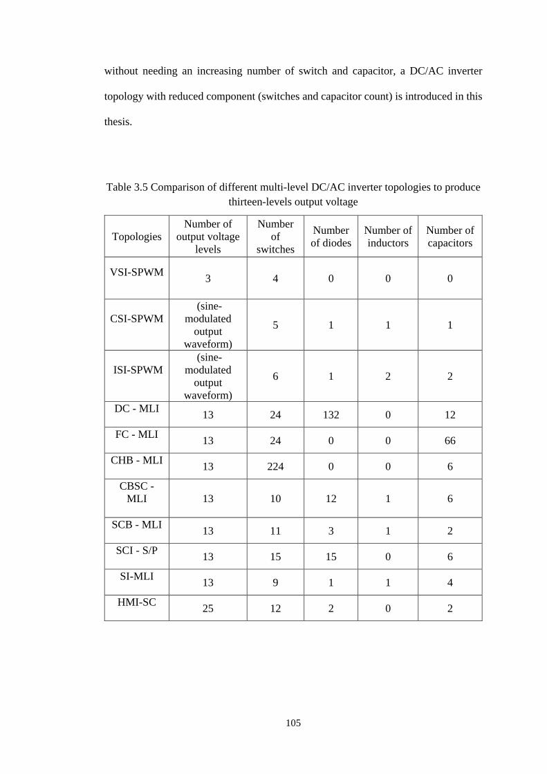
105
without needing an increasing number of switch and capacitor, a DC/AC inverter
topology with reduced component (switches and capacitor count) is introduced in this
thesis.
Table 3.5 Comparison of different multi-level DC/AC inverter topologies to produce thirteen-levels output voltage
Topologies Number of
output voltage levels
Number of
switches
Number of diodes
Number of inductors
Number of capacitors
VSI-SPWM 3 4 0 0 0
CSI-SPWM
(sine-modulated
output waveform)
5 1 1 1
ISI-SPWM
(sine-modulated
output waveform)
6 1 2 2
DC - MLI 13 24 132 0 12
FC - MLI 13 24 0 0 66
CHB - MLI 13 224 0 0 6
CBSC - MLI
13 10 12 1 6
SCB - MLI 13 11 3 1 2
SCI - S/P 13 15 15 0 6
SI-MLI 13 9 1 1 4
HMI-SC 25 12 2 0 2

106
Summary
This chapter presents a critical review of the switched capacitor technique in
addition to other voltage boosting techniques (magnetic coupling and multi-stage
booster) surveyed in published literature. It contains the classification of techniques
according to their circuit topology/configuration and connection. This chapter is
important in identifying the weaknesses and strengths of each of the covered
techniques and circuit topologies and/or configuration surveyed. These points are very
useful in providing a comparative study of each technique and circuit topology and/or
configuration surveyed in published literature. The comparative study shows that
switched-capacitor circuit (SCC) technique should be given special attention due to its
advantages in comparison with other techniques. Two types of comprehensive
mathematical analyses are performed on the resonant-based SCC DSSC configuration
with applied varying switch duty cycle control technique, showing its ability to behave
like a variable capacitor. This also shows its ability to vary/regulate voltage like a
voltage regulator. The relationship between effective capacitance and varying switch
duty cycle is presented. In addition, the relationship between varying voltage and
varying switch duty cycle is presented for this circuit configuration. Several
performance criteria are set by the author as guidelines to decide the optimum SCC
topology/technique to be integrated into the proposed inverter circuit. This provides a
comparative analysis that shows each technique and circuit topology and/or
configuration surveyed capable of satisfying the criteria assessed by the author. The
result/outcome showed the resonant-based SCC DSSC configuration has a specific
advantage over the others.
107
This chapter also presents a review of new evolved different DC/AC inverter
topologies/techniques over the last few years surveyed in published literature. The
weaknesses and strengths of each of the covered DC/AC inverter topologies are
identified. These points are very useful in providing a comparative study of each
technique and circuit topology and/or configuration surveyed in published literature.
The comparative study shows that generating higher voltage levels using multi-level
topologies/techniques (classical and new evolved) demands high component (power
switches, diodes, and capacitors) usage. Efforts made to reduce the number of
components in multi-level inverter topologies based switched-capacitor is given
special attention in this thesis. Therefore, a new simple inverter topology capable of
generating a high number of levels of near sinusoidal (multi-level/staircase) AC output
voltage with reduced component count will be proposed. This new DC/AC inverter
topology is introduced and discussed in detail in Chapter 4.
108
Chapter 4 Proposed DC/AC Inverter Circuit Topology and Control Technique
Introduction
Many existing multi-level inverters based switched-capacitor circuit (SCC)
with H-bridge topologies require large number of power switches and capacitors to
construct high numbers of voltage levels (DC multi-level bus voltage) in order to
minimise harmonics distortion in AC output voltage (Rozlan, Darwish, Sallama, &
Khodapanah, 2015) (Gupta, Ranjan, Bhatnagar, Sahu, & Jain, 2016) (Taghvaie, Adabi,
& Rezanejad, 2016 (Barzegarkhoo, Kojabadi, Zamiry, Vosoughi, & Chang, 2016)
(Zamiri, N Vosoughi, Hosseini, Barzegarkhoo, & Sabahi, 2016). This can increase the
complexity of the control circuit where each power switch is associated with a gate
drive unit (opto-isolator), MOSFET drive, and cooling unit (heat-sink). Hence, the
overall system is bulky and costly. In this chapter, the proposed inverter circuit with a
reduced component (power semiconductor switches, diodes, and capacitors) count is
introduced. The principle operation, design and analysis, and control technique of the
proposed inverter system are elaborated on in detail. The main idea is to utilise the
ability of the resonant-based DSSC SCC circuit that varies the DC input voltage by
variable switch duty cycle control technique as investigated in Chapter 3.

109
Proposed Inverter System
The proposed inverter system comprises a single-phase inverter circuit and an
open-loop control circuit. Figure 4.1 shows the block diagram of the proposed inverter
system. The proposed inverter circuit evolves from a single-phase current source (CSI)
circuit topology. It consists of two stages of power conversion. The resonant-based
DSSC SCC is introduced in the first stage. This is controlled in such a way that a
rectified sine wave appears across a fixed capacitor (C1) of this circuit. The H-Bridge
circuit is connected in the second stage to convert the waveform into a line-frequency
AC output. Both stages are connected in cascade.
The decision to accept resonant-based DSSC SCC configuration circuit is
based on the relationship between effective capacitance and variable switch duty cycle
control, as well as the relationship between voltage and duty cycle results obtained in
Chapter 3. This is illustrated in Figure 3.6 and 3.10 (in Chapter 3). The results show
that this circuit may exhibit voltage varying voltage behaviour by applying variable
switch duty cycle control technique. This led to adopting the resonant-based DSSC
SCC configuration to be inserted in the first stage of the new proposed inverter system.
The adoption of this circuit configuration is also due to its ability to comply with sets
of criteria as explained in Chapter 3, which justify its adoption into the new proposed
DC/AC inverter. Figure 4.2 shows the circuit diagram of the proposed inverter.
The resonant-based DSSC SCC is formed by a current source and a DSSC SCC
configuration. Where a current source contains a DC input voltage is connected in
series with an inductor (L) and internal resistance of inductor, (R1) is connected to the
input of the proposed inverter. DSSC circuit is formed by one capacitor (C1), two
switches (S1) and (S2). This circuit aims to generate a rectified near sine (multi-

110
level/staircase) voltage waveform by applying suitable control technique (variable
switch duty cycle control in appropriate switching timing).
It should be noted that this two-unidirectional semiconductor switch operates
in anti-parallel operation so that when (S1) is switched on, (S2) is off and vice versa
over one switching cycle, Ts. These two switches operate at relatively high switching
frequency i.e. < 50 kHz (high enough to smooth and narrow the capacitor ripple
voltages but not too high to limit switching losses). This switching frequency is
assigned as Fs. A diode (D) and a smoothing capacitor (C2) are also included into the
proposed inverter. These are mainly for voltage filtering purposes. A diode is placed
in between a two-stage circuit, which is used to clamp the voltage (maintain at positive
levels and prevent from reverse current), while a smoothing capacitor connected in
parallel to the output load is used to smooth the output ripple voltage. An H-bridge
circuit is formed by switches (S3, S4, S5 and S6) which are used to transform a rectified
voltage waveform across a capacitor of the DSSC Circuit (terminal point X-Y) into a
multi-level/staircase AC waveform, where the switches (S3 – S6) operate at a
fundamental line frequency of (50 Hz).

111
Figure 4.1 Circuit Block Diagram of Proposed Inverter System

106
Figure 4.2 Circuit diagram of the proposed inverter:
a) Current Source (DC voltage in series with Inductor L and inductor resistance R1)
b) DSSC SCC configuration circuit (terminal point X-Y) c) H-Bridge Circuit
d) Smoothing Capacitor e) Load
The following section discusses the operating modes of the proposed inverter system.
Operating Modes of the Proposed Inverter System
The proposed inverter is designed to produce multi-level/staircase AC output
voltage at fundamental line frequency. The inverter operation has two types of
operating frequency; the high switching period and the fundamental switching period.
In achieving AC output voltage, the proposed inverter circuit needs to operate in three
different modes. A rectified multi-level waveform needs to be first generated during
the first half cycle of the fundamental switching period. This process involves two
switching modes; Mode 1 and Mode 2. This rectified waveform will then be
transformed to sinusoidal AC waveform by H-bridge during Mode 3.

107
The proposed inverter is required to produce multi-level/staircase AC output
voltage at fundamental frequency 𝑓𝑓𝑜𝑜. The fundamental switching period is
𝑇𝑇𝑜𝑜 =1𝑓𝑓𝑜𝑜
(4.1)
The switching control of the power semiconductor switches in DSSC circuit has
constant chopping high-frequency operation, (i.e. 𝑓𝑓𝑠𝑠 > 10 kHz) and varying on-time,
𝑡𝑡𝑘𝑘. The high switching period is
𝑇𝑇𝑠𝑠 =1𝑓𝑓𝑠𝑠
(4.2)
The duty cycle 𝐷𝐷𝑘𝑘 of the switch S1 is defined as the ratio of on-time switch 𝑡𝑡𝑘𝑘 over
entire high switching period, 𝑇𝑇𝑠𝑠.
𝐷𝐷𝑘𝑘 =𝑡𝑡𝑘𝑘𝑇𝑇𝑠𝑠
(4.3)
with 𝑛𝑛 times repeating high switching period 𝑇𝑇𝑠𝑠, the capacitor is charged (voltage
exponentially rise) during 𝑡𝑡𝑘𝑘 = 𝐷𝐷𝑘𝑘𝑛𝑛𝑇𝑇𝑠𝑠 (on-time switch subinterval) and capacitor store
charges (voltage constant) during 𝑡𝑡𝑏𝑏 = (1 − 𝐷𝐷𝑘𝑘)𝑛𝑛𝑇𝑇𝑠𝑠 (off-time switch subinterval).
Therefore, the high switching period can also be expressed as
𝑇𝑇𝑠𝑠 = 𝑡𝑡𝑘𝑘 + 𝑡𝑡𝑏𝑏 = 𝐷𝐷𝑘𝑘𝑛𝑛𝑇𝑇𝑠𝑠 + (1 − 𝐷𝐷𝑘𝑘)𝑛𝑛𝑇𝑇𝑠𝑠 =1𝐹𝐹𝑠𝑠
(4.4)
108
where the number of repeating switching cycle,
𝑛𝑛 =𝑡𝑡𝑘𝑘𝐷𝐷𝑘𝑘𝑇𝑇𝑠𝑠
(4.5)
and time point 𝑡𝑡𝑘𝑘 = 𝐷𝐷𝑘𝑘𝑛𝑛𝑇𝑇𝑠𝑠
The proposed inverter is designed to operate in three circuit operating modes.
The process of generating a rectified multi-level waveform involves two switching
circuit modes, Mode 1 and Mode 2. Each circuit mode is operated in the transient state.
The piecewise-linear derivation DC transient analysis method (Mellitt & Rashid,
1974) is used for analysing the proposed inverter circuit behaviour in terms of voltage
and current in the cycle by cycle basis. Sets of the piecewise-linear equation are
established for each circuit operating mode within the repetitive cycle of operation.
The piecewise-linear DC transient derivation analysis for circuit operating Mode 1 and
2 is presented in the following equation:
The first mode (Mode 1) takes place during the first half cycle of the high
switching period(0 ≤ 𝑡𝑡𝑘𝑘 ≤ 𝐷𝐷𝑘𝑘𝑛𝑛𝑇𝑇𝑠𝑠). Figure 4.3 shows the equivalent circuit for Mode
1. When switch (S1, S3 and S6) are turned on and (S2, S4 and S5) are off, the diode (D)
is conducting (in forward biased). Both capacitors (C1) and (C2) are connected in
parallel and both are charged through inductor (L). The capacitor (C1) is desired to
have small capacitance (1µF) in order to achieve high voltage ripple across it. The
output capacitor (C2) would have large capacitance (i.e. > 80µF) which can be used as
a smoothing filter used to limit the ripple output voltage. These parallel-connected
capacitors form a total capacitance of (CT) which is the summation of (C1) and (C2).
The equivalent circuit can be simplified as shown in Figure 4.4. The connection forms
a switched parallel resonant-topology where inductor (L) and inductor series resistance

109
(R1) are connected in parallel to capacitors (CT) and load (Ro).
Figure 4.3 Equivalent Circuit for Mode 1
Figure 4.4 Simplified Equivalent Circuit for Mode 1
The instantaneous voltage for this Mode 1 is described by following equation :
𝑉𝑉𝑠𝑠 = 𝑖𝑖𝐿𝐿1(𝑡𝑡)𝑅𝑅1 + 𝐿𝐿𝑑𝑑𝑖𝑖𝐿𝐿1(𝑡𝑡)𝑑𝑑𝑡𝑡
+ 𝑣𝑣𝐶𝐶𝐶𝐶1(𝑡𝑡)
(4.6)
𝑉𝑉𝑠𝑠 = 𝑖𝑖𝐿𝐿1(𝑡𝑡)𝑅𝑅1 + 𝐿𝐿𝑑𝑑𝑖𝑖𝐿𝐿1(𝑡𝑡)𝑑𝑑𝑡𝑡
+ 1𝐶𝐶𝐶𝐶 𝑖𝑖𝑐𝑐𝐶𝐶 𝑑𝑑𝑡𝑡 + 𝑣𝑣𝐶𝐶𝐶𝐶1(𝑡𝑡 = 0)
(4.7)

110
where initial condition 𝑖𝑖𝐿𝐿1(𝑡𝑡 = 0) = 𝐼𝐼𝐿𝐿1 and 𝑣𝑣𝐶𝐶𝐶𝐶(𝑡𝑡 = 0) = 𝑉𝑉𝑐𝑐1
The inductor current 𝑖𝑖𝐿𝐿1(𝑡𝑡) can be expressed as
𝑖𝑖𝐿𝐿1(𝑡𝑡) = 𝐼𝐼0 + 𝑒𝑒−𝑅𝑅1𝐿𝐿 𝑡𝑡 𝐼𝐼𝐿𝐿1 − 𝐼𝐼0 cos(𝜔𝜔𝑟𝑟𝑡𝑡)
+(2𝑉𝑉𝑠𝑠 − 𝑉𝑉𝑐𝑐1) − 𝑅𝑅𝐼𝐼𝐿𝐿1 + 𝐼𝐼0
2𝜔𝜔𝑟𝑟𝐿𝐿 sin(𝜔𝜔𝑟𝑟𝑡𝑡)
(4.8)
The capacitor voltage 𝑣𝑣𝑐𝑐𝐶𝐶1(𝑡𝑡) can be expressed as
𝑣𝑣𝐶𝐶𝐶𝐶1(𝑡𝑡) = 𝑉𝑉𝑠𝑠 − 𝐼𝐼0𝑅𝑅1
+ 𝑒𝑒−𝑅𝑅1𝐿𝐿 𝑡𝑡 𝑉𝑉𝑐𝑐1 − 𝑉𝑉𝑠𝑠 +
𝑅𝑅1𝐼𝐼0 − 𝐼𝐼𝐿𝐿1 2 cos(𝜔𝜔𝑟𝑟𝑡𝑡)
+ 𝑅𝑅1
2𝜔𝜔𝑟𝑟𝐿𝐿𝑉𝑉𝑐𝑐1 − 𝑉𝑉𝑠𝑠 +
𝑅𝑅1𝐼𝐼0 − 𝐼𝐼𝐿𝐿1 2
+ 𝜔𝜔𝑟𝑟 𝐼𝐼0 − 𝐼𝐼𝐿𝐿1 sin(𝜔𝜔𝑟𝑟𝑡𝑡)
(4.9)
At the end of this mode
𝑖𝑖𝐿𝐿1(𝑡𝑡𝑘𝑘 = 𝐷𝐷𝑘𝑘𝑛𝑛𝑇𝑇𝑠𝑠) = 𝐼𝐼𝐿𝐿2
𝑣𝑣𝐶𝐶𝐶𝐶1(𝑡𝑡𝑘𝑘 = 𝐷𝐷𝑘𝑘𝑛𝑛𝑇𝑇𝑠𝑠) = 𝑉𝑉𝑐𝑐2
(4.10)
The second mode (Mode 2) takes place during the second half cycle of the high
switching period (𝐷𝐷𝑘𝑘𝑛𝑛𝑇𝑇𝑠𝑠 ≤ 𝑡𝑡𝑏𝑏 ≤ (1 − 𝐷𝐷𝑘𝑘)𝑛𝑛𝑇𝑇𝑠𝑠 ). It should be noted that both Mode 1
and 2 are operated during the first half cycle of fundamental switching period
0 ≤ 𝑡𝑡 ≤ 𝐶𝐶𝑜𝑜2
. Figure 4.5 shows the equivalent circuit for Mode 2 which forms an (R-
L) circuit. When switches (S2, S3 and S6) are turned on and (S1, S4 and S5) are off, the
diode (D) is in reverse biased, disconnecting the load from input. The capacitor (C1) is
disconnected and voltage across it will remain constant (in this particular condition
mode, the capacitor charge is stored for the duration 𝑡𝑡𝑏𝑏). The capacitor (C2) is

111
connected in series with load (Ro). It should be noted that, both Mode 1 and 2 are
operated during the first half cycle of fundamental switching period0 ≤ 𝑡𝑡 ≤ 𝐶𝐶𝑜𝑜2
.
Figure 4.5 Equivalent Circuit for Mode 2
The instantaneous voltage for this Mode 2 is described by the following equation:
𝑉𝑉𝑠𝑠 = 𝑖𝑖𝐿𝐿2(𝑡𝑡)𝑅𝑅1 + 𝐿𝐿𝑑𝑑𝑖𝑖𝐿𝐿2(𝑡𝑡)𝑑𝑑𝑡𝑡
(4.11)
Redefine the time origin, 𝑡𝑡 = 0, the initial condition 𝑖𝑖𝐿𝐿2(𝑡𝑡 = 0) = 𝐼𝐼𝐿𝐿2 and 𝑣𝑣𝑐𝑐2(𝑡𝑡 = 0) = 𝑉𝑉𝑐𝑐2
The inductor current 𝑖𝑖𝐿𝐿2(𝑡𝑡) can be expressed as
𝑖𝑖𝐿𝐿2(𝑡𝑡) =𝑉𝑉𝑠𝑠𝑅𝑅11 − 𝑒𝑒−
𝑅𝑅1𝐿𝐿 𝑡𝑡 + 𝐼𝐼𝐿𝐿2 𝑒𝑒−
𝑅𝑅1𝐿𝐿 𝑡𝑡
(4.12)
The capacitor voltage 𝑣𝑣𝑐𝑐2(𝑡𝑡) can be expressed as
𝑣𝑣𝑐𝑐2(𝑡𝑡) = 𝑉𝑉𝑐𝑐2 𝑒𝑒−1
𝑅𝑅𝑜𝑜𝐶𝐶2𝑡𝑡
(4.13)
The capacitor (C2) discharge its initial energy stored to load (Ro) while the initial
energy remains stored in Capacitor (C1)

112
At the end of this mode
𝑖𝑖𝐿𝐿2(𝑡𝑡𝑏𝑏 = (1 − 𝐷𝐷𝑘𝑘)𝑛𝑛𝑇𝑇𝑠𝑠) = 𝐼𝐼𝐿𝐿3
𝑣𝑣𝑐𝑐2(𝑡𝑡𝑏𝑏 = (1 − 𝐷𝐷𝑘𝑘)𝑛𝑛𝑇𝑇𝑠𝑠) = 𝑉𝑉𝑐𝑐3
(4.14)
The switch operation is repeated for 𝑛𝑛 times switching cycle in previous equation (4.5)
where time point, 𝑡𝑡𝑘𝑘 will be determined later. This will be discussed in detail during
the determination of switching time in next Switching Control section. The duration
of the square pulse signal to be applied to the switch (S1) (switch duty cycle) in DSSC
circuit can be controlled which is valid for specific time intervals (control the amount
of charge to be stored in the fixed capacitor (C1) i.e. controlling the capacitor charging).
Applying different duty cycle control values to the associated switch, different
transient capacitor voltage levels (multi-level voltage waveform) can be obtained
across capacitor (C1). The repeating switching action between circuit modes can create
ripple voltage across DSSC circuit (terminal X-Y). The peak-to-peak voltage across
point terminal X-Y can become larger when the duration of the square pulse signals is
increased with time point, 𝑡𝑡𝑘𝑘. At the output of this circuit, this ripple voltage can be
filtered by smoothing capacitor (C2) which is connected in parallel to the load.
Therefore, a rectified multi-level voltage waveform can be shaped by applying
different duty cycle values which valid in specific timing control. Different duty cycle
mode values can be achieved by comparing different DC levels (Vdck) (as references
signal) with a high-frequency triangular carrier signal (Vtri). This creates a switching
control pattern (or gating signals), and this proposed control technique is called
variable switch duty cycle control. The gating signals are to be fed to the switches in
the DSSC SCC circuit. This is elaborated on in detail in the following control
technique section. A multi-level/staircase waveform can be generated by using

113
variable switch duty cycle control technique (variable duty cycle control in specific
switching timing).
The third mode (Mode 3) taking place during the second half cycle of the
fundamental switching period 𝐶𝐶𝑜𝑜2≤ 𝑡𝑡 ≤ 𝑇𝑇𝑜𝑜 . The H-bridge switches (S3 and S6)
transform a rectified multi-level voltage waveform into a sinusoidal AC output voltage
waveform.
Design & Analysis
The resonant-based DSSC SCC circuit with variable switch duty cycle control
technique demonstrated the ability to vary the DC input voltage, as investigated in
Chapter 3. This behaves like a voltage regulator. By using variable switch duty cycle
control in specific switching timing, the voltage across resonant-based DSSC SCC
circuit can be varied/regulated in such a way that rectified near sine (multi-
level/staircase) voltage waveform can be generated/shaped across a fixed capacitor
(C1) of this circuit. Assuming ideal staircase shape of the capacitor voltage steps
(neglect the transient in capacitor voltage). The design procedure and example is
shown in the following section, showing the formation of rectified multi-
level/staircase voltage waveform across (C1) of the DSSC circuit (terminal X-Y) and
eventually multi-level/staircase AC voltage waveform across the load.

114
4.4.1 Design Procedure of the Proposed Inverter
A new proposed DC/AC inverter output voltage waveform is desired to have
output waveform as close to sinusoidal waveform as possible, so that minimum
harmonics distortion can be achieved. In theory, the sinusoidal voltage is given by
𝑉𝑉𝑜𝑜(𝑡𝑡𝑘𝑘) = 𝑉𝑉𝑖𝑖 sin(𝜔𝜔𝑡𝑡𝑘𝑘)
(4.15)
where,
𝑉𝑉𝑜𝑜(𝑡𝑡) is the output voltage
𝑉𝑉𝑖𝑖 is the peak amplitude of the output voltage
𝜔𝜔 is the angular frequency in radians per second (rad/seconds)
𝑡𝑡𝑘𝑘 is the time
In order to trace the sine waveform, the output voltage of the new proposed DC/AC
inverter can be divided into 𝑚𝑚 voltage levels with respect to 𝑘𝑘-th switching time which
can be expressed as
𝑉𝑉𝑜𝑜(𝑡𝑡𝑘𝑘) = 𝑉𝑉2𝑘𝑘𝑁𝑁
, 𝑘𝑘 ≤ 𝑁𝑁
𝑉𝑉2𝑁𝑁−𝑘𝑘3
, 𝑁𝑁 < 𝑘𝑘 ≤ 2𝑁𝑁
(4.16)
where
𝑡𝑡𝑘𝑘 = 𝑡𝑡1, 𝑡𝑡2, … . … . , 𝑡𝑡2𝑁𝑁 is the switching time (or time point)
𝑘𝑘 = 1,2, …𝑁𝑁 and 𝑁𝑁 = 𝑚𝑚−12
𝑚𝑚 is number of voltage levels (include zero level).
Hence, for 𝑚𝑚-level staircase/multi-level AC output voltage, there are 𝑁𝑁-main voltage
steps of a staircase rectified voltage waveform.

115
Using equation (4.16). The output voltage is given by
𝑉𝑉𝑜𝑜(𝑡𝑡𝑘𝑘) = 𝑉𝑉2𝑘𝑘𝑁𝑁
, … . ,𝑉𝑉2 , … . ,𝑉𝑉2𝑘𝑘𝑁𝑁 (4.17)
and the switching time (or time point) for positive half cycle of the fundamental
switching period 𝑇𝑇𝑜𝑜 is denote as
𝑡𝑡𝑘𝑘 = 𝑡𝑡𝑘𝑘, … . , 𝑡𝑡𝑁𝑁, … . , 𝑡𝑡2𝑁𝑁
(4.18)
Or in another form the output voltage is given by
𝑉𝑉𝑜𝑜(𝑡𝑡𝑘𝑘) =
⎩⎪⎪⎪⎨
⎪⎪⎪⎧𝑉𝑉2𝑘𝑘𝑁𝑁
, 𝑡𝑡𝑘𝑘 ≤ 𝑡𝑡 ≤ 𝑡𝑡𝑘𝑘+1...
𝑉𝑉2 , 𝑡𝑡𝑁𝑁 < 𝑡𝑡 ≤ 𝑡𝑡𝑁𝑁+1.. .
𝑉𝑉2𝑘𝑘𝑁𝑁
, 𝑡𝑡2𝑁𝑁−1 < 𝑡𝑡 ≤ 𝑡𝑡2𝑁𝑁
(4.19)
The first 𝑁𝑁-main voltage steps can be described by the piece-wise expression:
𝑉𝑉𝑜𝑜 (𝑝𝑝𝑐𝑐𝑎𝑎𝑘𝑘) = 𝑉𝑉𝑘𝑘
𝑁𝑁
𝑘𝑘=1
(𝑡𝑡𝑘𝑘 ) = 𝑉𝑉2𝑘𝑘𝑁𝑁
(𝑡𝑡1 )+. . … . .𝑉𝑉2 (𝑡𝑡𝑁𝑁 )
(4.20)
which can also be expressed as
𝑉𝑉(0 ) = 0
𝑉𝑉2𝑘𝑘𝑁𝑁
(𝑡𝑡1 ) = 𝑣𝑣𝑐𝑐1(𝑡𝑡1) + 𝑉𝑉(0 )
.
.
..
𝑉𝑉2 (𝑡𝑡𝑁𝑁 ) = 𝑣𝑣𝑐𝑐𝑁𝑁(𝑡𝑡𝑁𝑁) + 𝑉𝑉2(𝑁𝑁−1)𝑁𝑁
(𝑡𝑡𝑁𝑁−1 )
(4.21)

116
where
𝑣𝑣𝑐𝑐1(𝑡𝑡1) to 𝑣𝑣𝑐𝑐𝑁𝑁(𝑡𝑡𝑁𝑁) are the capacitor voltages level which can also be represented as
voltage increment as shown in equation (3.37).
m is number of voltage levels (include zero level).
𝑉𝑉2 (𝑡𝑡𝑁𝑁 ) represent the peak maximum voltage level of the output phase voltage.
A near AC (staircase/multi-level) output voltage 𝑉𝑉𝑜𝑜(𝑡𝑡𝑘𝑘) waveform needs to be shaped
close to sinusoidal waveform. To obtain low total harmonic distortion in output voltage
VTHD, the switching time or angle is determined by using the Half-Height method (Luo
and Ye, 2013). This method can arrange the main switching angle in simple way
according to the sine function. For known 𝑘𝑘-th staircase steps/levels of sine wave
output voltage, the corresponding switching time at that particular intersection voltage
levels can be set. The switching time during the positive cycle of the output voltage
waveform, 𝑡𝑡𝑘𝑘 = 𝑇𝑇𝑜𝑜2
(or 10 ms) is defined as the main switching time (or time point)
𝑡𝑡𝑘𝑘 = 𝑡𝑡1, … . ,tN which can be determined by the formula,
𝑡𝑡𝑘𝑘 (in milisecond) = sin−1 2k − 1m − 1
×10𝑚𝑚𝑚𝑚180°
= 𝐷𝐷𝑘𝑘𝑛𝑛𝑇𝑇𝑠𝑠 (4.22)
where k = 1,2, … N and N = 𝑚𝑚−12
and m is peak-to-peak output voltage level (include zero)
During the negative cycle of the output voltage waveform, 𝑇𝑇𝑜𝑜
2< 𝑡𝑡𝑘𝑘 < 𝑇𝑇𝑜𝑜 (10ms to
20ms), the switching time (or time point) 𝑡𝑡𝑘𝑘 = 𝑡𝑡𝑘𝑘+1, … . ,𝑡𝑡2𝑁𝑁 can be determined by
using the following formula
𝑡𝑡𝑘𝑘+1 (in milisecond ms) = 𝜋𝜋 − 𝑡𝑡𝑘𝑘 = 10𝑚𝑚𝑚𝑚 − 𝑡𝑡𝑘𝑘 (4.23)
𝑡𝑡7 (in milisecond ms) = 𝜋𝜋 − 𝑡𝑡6 = 10𝑚𝑚𝑚𝑚 − 𝑡𝑡6

117
𝑡𝑡8 (in milisecond ms) = 𝜋𝜋 − 𝑡𝑡5 = 10𝑚𝑚𝑚𝑚 − 𝑡𝑡5
.
𝑡𝑡11 (in milisecond ms) = 𝜋𝜋 − t2 = 10𝑚𝑚𝑚𝑚 − t2
𝑡𝑡2𝑁𝑁 (in milisecond ms) = 𝜋𝜋 − t1 = 10𝑚𝑚𝑚𝑚 − t1
(4.24)
4.4.2 Fourier Analysis
The harmonics content of the output voltage can be determined by using Fourier
series:
𝑉𝑉0(𝑡𝑡) = 𝑎𝑎0 + (𝑎𝑎𝑛𝑛 cos 𝑛𝑛(𝜔𝜔𝑡𝑡) + 𝑏𝑏𝑛𝑛 sin𝑛𝑛(𝜔𝜔𝑡𝑡))∞
𝑛𝑛=1
(4.25)
The output voltage 𝑉𝑉0(𝑡𝑡) is an odd function, 𝑎𝑎𝑛𝑛 = 0 and
𝑏𝑏𝑛𝑛 =2T 𝑉𝑉0(𝑡𝑡) sin 𝑛𝑛(𝜔𝜔𝑡𝑡)𝐶𝐶
0𝑑𝑑𝑡𝑡
(4.26)
Substituting equation (4.16) into equation (4.26), 𝑏𝑏𝑛𝑛 can be expressed as
𝑏𝑏𝑛𝑛 = 𝑉𝑉2𝑘𝑘𝑁𝑁
𝑁𝑁
𝑥𝑥=1
(cos𝑛𝑛(𝜔𝜔𝑡𝑡𝑥𝑥) − cos𝑛𝑛(𝜔𝜔𝑡𝑡𝑥𝑥+1))
+ 𝑉𝑉2𝑁𝑁−𝑘𝑘3
2𝑁𝑁
𝑥𝑥=𝑁𝑁+1
cos𝑛𝑛𝜔𝜔𝑡𝑡𝑥𝑥 − cos𝑛𝑛𝜔𝜔𝑡𝑡𝑥𝑥+1
(4.27)
To assess the harmonics spectrum of inverter output, the total harmonic distortion
(THD) is a parameter index used to assess harmonics distortion. The THD of a voltage
waveform is defined as
𝑇𝑇𝐻𝐻𝐷𝐷 = ∑ 𝑏𝑏𝑛𝑛
2∞𝑛𝑛=2
𝑏𝑏12
(4.28)

118
where 𝑏𝑏1 and 𝑏𝑏𝑛𝑛 are the fundamental voltage and nth harmonics voltage components.
4.4.3 Design Example and Calculation of the Proposed Inverter
For the proposed/designed thirteen-levels inverter, the thirteen-levels (𝑚𝑚 =
13) staircase/multi-level AC output voltage over half cycle of fundamental period can
be generated by using equations (4.16) and (4.17), the output voltage is given by
𝑉𝑉𝑜𝑜(𝑡𝑡𝑘𝑘) = 𝑉𝑉13
,𝑉𝑉23
,𝑉𝑉1 ,𝑉𝑉43
,𝑉𝑉53
,𝑉𝑉2 ,𝑉𝑉53
,𝑉𝑉43
,𝑉𝑉1 ,𝑉𝑉23
,𝑉𝑉13
(4.29)
and the switching time (or time point) for half cycle of fundamental period, 𝑇𝑇𝑜𝑜 are
denote as
𝑡𝑡𝑘𝑘 = 𝑡𝑡1, 𝑡𝑡2, 𝑡𝑡3, 𝑡𝑡4, 𝑡𝑡5, 𝑡𝑡6, 𝑡𝑡7, 𝑡𝑡8, 𝑡𝑡9, 𝑡𝑡10, 𝑡𝑡11, 𝑡𝑡12
(4.30)
Using equation (4.20), the six-main voltage steps of the staircase/multi-level output
voltage over half cycle of fundamental period, 𝑇𝑇𝑜𝑜 can be represent as
𝑉𝑉𝑜𝑜(𝑡𝑡𝑘𝑘) =
⎩⎪⎪⎪⎪⎪⎪⎨
⎪⎪⎪⎪⎪⎪⎧𝑉𝑉13
, 𝑡𝑡1 ≤ 𝑡𝑡𝑘𝑘 ≤ 𝑡𝑡2𝑉𝑉23
, 𝑡𝑡2 ≤ 𝑡𝑡𝑘𝑘 ≤ 𝑡𝑡3𝑉𝑉1 , 𝑡𝑡3 ≤ 𝑡𝑡𝑘𝑘 ≤ 𝑡𝑡4𝑉𝑉43
, 𝑡𝑡4 ≤ 𝑡𝑡𝑘𝑘 ≤ 𝑡𝑡5𝑉𝑉53
, 𝑡𝑡5 < 𝑡𝑡𝑘𝑘 ≤ 𝑡𝑡6𝑉𝑉2 , 𝑡𝑡6 < 𝑡𝑡𝑘𝑘 ≤ 𝑡𝑡7𝑉𝑉53
, 𝑡𝑡7 < 𝑡𝑡𝑘𝑘 ≤ 𝑡𝑡8𝑉𝑉43
, 𝑡𝑡8 < 𝑡𝑡𝑘𝑘 ≤ 𝑡𝑡9𝑉𝑉1 , 𝑡𝑡9 < 𝑡𝑡𝑘𝑘 ≤ 𝑡𝑡10𝑉𝑉23
, 𝑡𝑡10 ≤ 𝑡𝑡𝑘𝑘 ≤ 𝑡𝑡11𝑉𝑉13
, 𝑡𝑡11 < 𝑡𝑡𝑘𝑘 ≤ 𝑡𝑡12
(4.31)
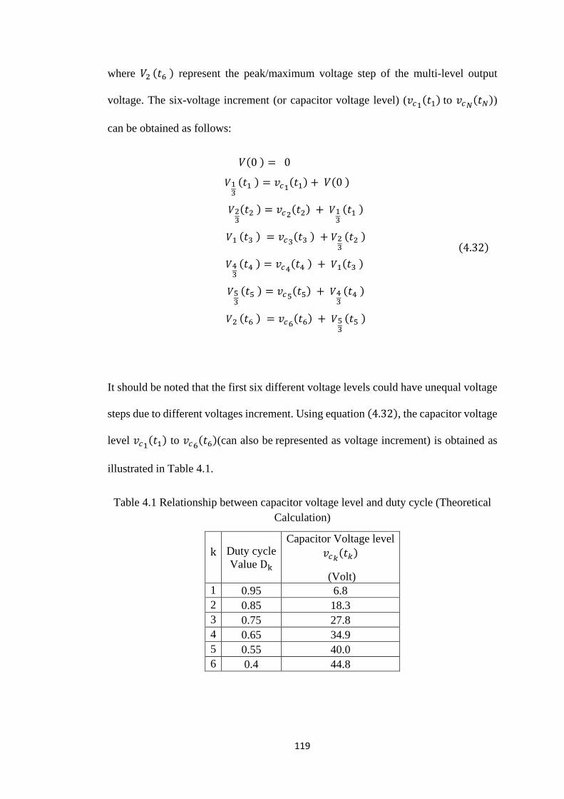
119
where 𝑉𝑉2 (𝑡𝑡6 ) represent the peak/maximum voltage step of the multi-level output
voltage. The six-voltage increment (or capacitor voltage level) (𝑣𝑣𝑐𝑐1(𝑡𝑡1) to 𝑣𝑣𝑐𝑐𝑁𝑁(𝑡𝑡𝑁𝑁))
can be obtained as follows:
𝑉𝑉(0 ) = 0
𝑉𝑉13
(𝑡𝑡1 ) = 𝑣𝑣𝑐𝑐1(𝑡𝑡1) + 𝑉𝑉(0 )
𝑉𝑉23
(𝑡𝑡2 ) = 𝑣𝑣𝑐𝑐2(𝑡𝑡2) + 𝑉𝑉13
(𝑡𝑡1 )
𝑉𝑉1 (𝑡𝑡3 ) = 𝑣𝑣𝑐𝑐3(𝑡𝑡3 ) + 𝑉𝑉23
(𝑡𝑡2 )
𝑉𝑉43
(𝑡𝑡4 ) = 𝑣𝑣𝑐𝑐4(𝑡𝑡4 ) + 𝑉𝑉1(𝑡𝑡3 )
𝑉𝑉53
(𝑡𝑡5 ) = 𝑣𝑣𝑐𝑐5(𝑡𝑡5) + 𝑉𝑉43
(𝑡𝑡4 )
𝑉𝑉2 (𝑡𝑡6 ) = 𝑣𝑣𝑐𝑐6(𝑡𝑡6) + 𝑉𝑉53
(𝑡𝑡5 )
(4.32)
It should be noted that the first six different voltage levels could have unequal voltage
steps due to different voltages increment. Using equation (4.32), the capacitor voltage
level 𝑣𝑣𝑐𝑐1(𝑡𝑡1) to 𝑣𝑣𝑐𝑐6(𝑡𝑡6)(can also be represented as voltage increment) is obtained as
illustrated in Table 4.1.
Table 4.1 Relationship between capacitor voltage level and duty cycle (Theoretical Calculation)
k Duty cycle
Value Dk
Capacitor Voltage level 𝑣𝑣𝑐𝑐𝑘𝑘(𝑡𝑡𝑘𝑘)
(Volt) 1 0.95 6.8 2 0.85 18.3 3 0.75 27.8 4 0.65 34.9 5 0.55 40.0 6 0.4 44.8
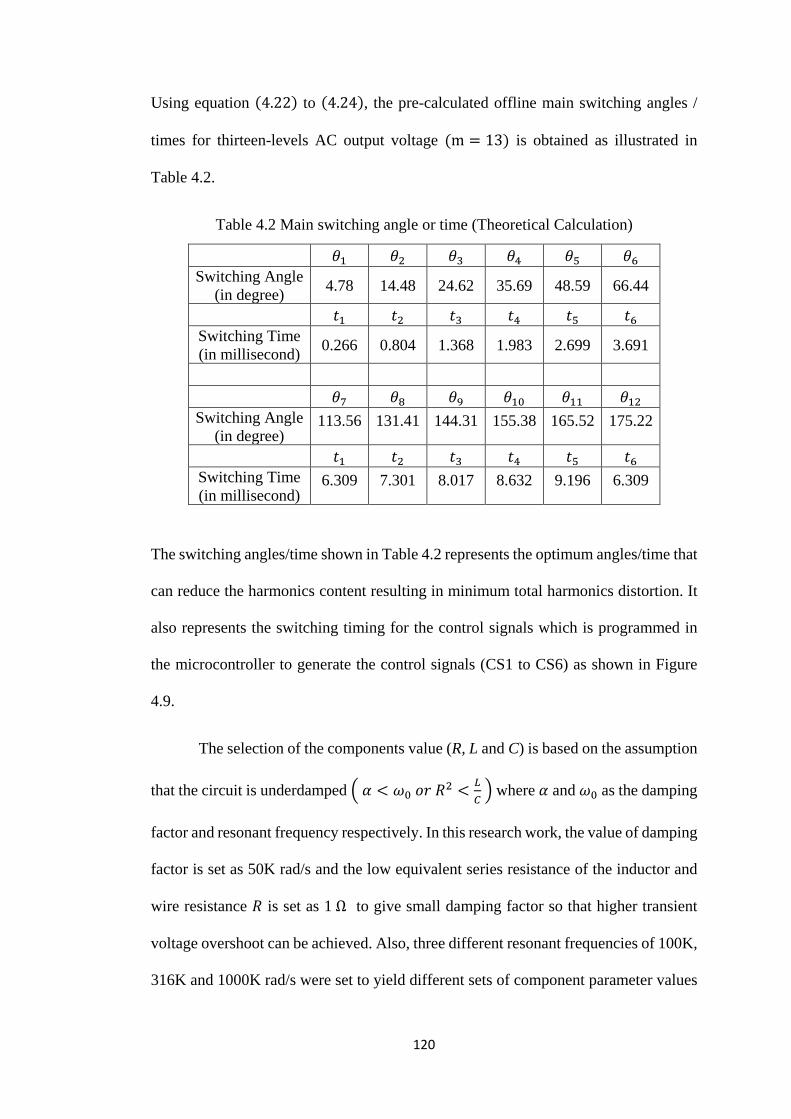
120
Using equation (4.22) to (4.24), the pre-calculated offline main switching angles /
times for thirteen-levels AC output voltage (m = 13) is obtained as illustrated in
Table 4.2.
Table 4.2 Main switching angle or time (Theoretical Calculation)
𝜃𝜃1 𝜃𝜃2 𝜃𝜃3 𝜃𝜃4 𝜃𝜃5 𝜃𝜃6 Switching Angle
(in degree) 4.78 14.48 24.62 35.69 48.59 66.44
𝑡𝑡1 𝑡𝑡2 𝑡𝑡3 𝑡𝑡4 𝑡𝑡5 𝑡𝑡6 Switching Time (in millisecond) 0.266 0.804 1.368 1.983 2.699 3.691
𝜃𝜃7 𝜃𝜃8 𝜃𝜃9 𝜃𝜃10 𝜃𝜃11 𝜃𝜃12
Switching Angle (in degree)
113.56 131.41 144.31 155.38 165.52 175.22
𝑡𝑡1 𝑡𝑡2 𝑡𝑡3 𝑡𝑡4 𝑡𝑡5 𝑡𝑡6 Switching Time (in millisecond)
6.309 7.301 8.017 8.632 9.196 6.309
The switching angles/time shown in Table 4.2 represents the optimum angles/time that
can reduce the harmonics content resulting in minimum total harmonics distortion. It
also represents the switching timing for the control signals which is programmed in
the microcontroller to generate the control signals (CS1 to CS6) as shown in Figure
4.9.
The selection of the components value (R, L and C) is based on the assumption
that the circuit is underdamped 𝛼𝛼 < 𝜔𝜔0 𝑜𝑜𝑜𝑜 𝑅𝑅2 < 𝐿𝐿𝐶𝐶
where 𝛼𝛼 and 𝜔𝜔0 as the damping
factor and resonant frequency respectively. In this research work, the value of damping
factor is set as 50K rad/s and the low equivalent series resistance of the inductor and
wire resistance 𝑅𝑅 is set as 1 Ω to give small damping factor so that higher transient
voltage overshoot can be achieved. Also, three different resonant frequencies of 100K,
316K and 1000K rad/s were set to yield different sets of component parameter values

121
range of options (Case 1,2 and 3) which can obtain low THD output. By substituting
the damping ratio, resonant frequency, the capacitor voltage levels and switching time
obtained (as illustrated in Table 4.1 and 4.2) into equation (3.32), three different cases
of parameter components values of L, C1 and C2 can be determined as follows:
Case 1: R1=1Ω, L=10µH, C1=10µF, C2=100uF, R𝑜𝑜=10Ω
Case 2: R1=1Ω, L=10 µH, C1=1µF, C2=100µF, R𝑜𝑜=10Ω
Case 3: R1=1Ω, L=10uH, C1=0.1µF, C2=100µF, R𝑜𝑜=10Ω
Using equation (4.28), the voltage THD for designed thirteen-levels inverter is
obtained. The relationship between voltage THD and high switching frequency (DSSC
SCC circuit) for three different cases is plotted in Figure 4.6.
Figure 4.6 Percentage of THD of output voltage VTHD in terms of high switching
frequency
For a thirteen-levels proposed inverter, the component parameter Case 1 is
chosen that can consistently provide low THD performance for wide switching
frequency operation (10 kHz ≤ 𝑓𝑓𝑠𝑠 ≤ 70 kHz) of the DSSC circuit. Under pure resistive
load (Ro =10 Ω), the lowest VTHD can be obtained when DSSC circuit operating at 10
0
10
20
30
40
50
60
0 10 20 30 40 50 60 70 80 90 100
Perc
enta
ge o
f VT
HD
(%
)
Switching Frequency, 𝑓𝑓𝑚𝑚 (kHz)
Case 1Case 2Case 3

122
kHz switching frequency 𝑓𝑓𝑠𝑠. The estimated calculation THD output voltage (VTHD) is
4.6 % as shown in Figure 4.6 (Case 1 (Green)). Therefore, Case 1 is chosen to be use
in design simulation of the proposed DC/AC inverter in Chapter 5.
Proposed Control Technique
This section explains the control technique used for the proposed DC/AC
inverter. The formation of a near AC (staircase/multi-level) voltage involves two
processes:
1) To generate full rectified multi-level waveform during the positive cycle of the
AC output.
2) To transform generated rectified multi-level waveform into complete near
multi-level AC voltage waveform.
Different transient capacitor voltage levels (multi-level voltage) can be obtained by
suitably charging a fixed capacitor (C1) in the resonant-based DSSC SCC circuit (in
Figure 4.2). This charging capacitor can be controlled by the proposed open-loop
control circuit shown in Figure 4.1 and Figure 4.7. The control logic circuit outputs
two PWM signals labelled as S1 and S2 which are responsible for controlling the
charging capacitor (C1) through switches (S1) and (S2). These switches have anti-
parallel operation i.e. when (S1) is turned on, (S2) is off and vice versa. The variable
switch duty cycle control PWM technique is proposed to generate control signals for
switches (S1) and (S2). The variable switch duty cycle control PWM technique is
variable switch duty cycle control in specific switching timing. This technique is used
to obtain a variable switch duty cycle PWM control signal. This is achieved by
comparing fundamental frequency multi-level DC waveform (reference signal) to the

123
high-frequency triangular waveform (carrier signal). Each step of the multi-level DC
waveform (reference signal) is controlled in specific switching timing. Figure 4.8
shows the control logic circuit used to generate the variable switch duty cycle PWM
control signal. This control signal will be applied to the control switches of the
resonant-based DSSC circuit so that six transient voltage steps/levels of the rectified
staircase/multi-level waveform (thirteen-levels peak-to-peak output voltage) can be
generated during the positive cycle of the fundamental period (0 to 10 ms).
The circuit comprises six AND gates, six comparators (Op-Amp), single OR
gate, and single NOT (inverter) gate to produce pulse train signals at six different duty
cycle modes. These pulse train signals can be divided into two control signals. The
first control signal S1 will be applied to switch (S1) of the resonant-based DSSC circuit.
The second control signal S2 will be applied to switch (S2) via a NOT (inverter) gate.
The input signals (Vdc1 to Vdc6) (signals at six different DC voltage levels) and control
signals (CS1 to CS6) are the input signals to be fed to the control circuit. (CS1 to CS6)
are pre-programmed in microcontroller according to the main switching time
calculated above. These microcontroller output signals are then multiplied by (Vdc1 to
Vdc6) through AND gates so that reference signals (RS1-RS6) can be generated. PWM
gating signals (with different duty cycle modes (D1 to D6)) can be generated by
comparing reference signal (RS1-RS6) with triangular carrier signal (10 kHz ≤ 𝑓𝑓𝑠𝑠≤ 70
kHz) using comparator (Op Amp) as shown in Figure 4.8.
The PWM signal (D1 to D3) is applied to the switch S1 to step-up capacitor
voltage in three transient voltage steps/levels during the first quarter cycle of AC
output waveform (0 to 5ms). The maximum voltages can be reached during duty cycle
when mode 3 (D3) is applied (where the determination of capacitance (C1) is based on
this maximum voltage). During the second quarter cycle of the fundamental period

124
(5ms to 10ms), the PWM signal (D3 to D6) is applied to the switch S1 step-down
capacitor voltage in three transient voltage steps/levels. OR gate is used to combine
each PWM signal (D1 to D6).
Figure 4.7 Control logic circuit for DSSC circuit
This PWM signal is called variable switch duty cycle PWM control signal (S1). The
signal (S2) is the inverted signal of (S1) via inverter gate. A hard-limiter is used to
obtain a square wave gating pulse. The variable switch duty cycle PWM control signal
is applied to switch (S1) and (S2) through isolating circuit (opto-isolator).
Figures 4.9 and 4.10 shows the example of 2 kHz control signals. The pulse
train signal S2 represents the inverted signal of S1. Figures 4.9 and 4.10 show the

125
theoretical timing diagram of the variable switch duty cycle PWM control signals S1
and S2 with variable amplitude modulation 𝑚𝑚𝑎𝑎𝑘𝑘 is shown in Table 4.3 and the
frequency modulation 𝑚𝑚𝑓𝑓 of 200. These output signals are generated from control
circuit in Figure 4.8 to be fed to switches (S1) and (S2) in the resonant-based DSSC
circuit. The switch duty cycle, which is also called amplitude modulation ratio 𝑚𝑚𝑎𝑎 can
be calculated using formula (4.33). 𝑚𝑚𝑎𝑎𝑘𝑘 is the ratio of the different DC levels in multi-
level DC waveform (amplitude of reference signal) to the amplitude of a triangular
waveform (amplitude of carrier signal). The frequency modulation ratio 𝑚𝑚𝑓𝑓 is the ratio
of the frequency of triangular waveform (frequency of the carrier signal) to the
frequency of multi-level DC waveform (frequency of the reference signal). This can
be calculated using equation (4.34).
Amplitude Modulation,𝑚𝑚𝑎𝑎𝑘𝑘 =VrefVtri
=VdckVtri
(4.33)
Frequency Modulation,𝑚𝑚𝑓𝑓 =FtriFref
(4.34)
where,
The gating pulse S1 = 1, when Vdck > Vtri(carrier)
The gating pulse S1 = 0, when Vdck < Vtri(carrier)
Vtri is the amplitude of the carrier signal (10 Volts)
Vdck is the different DC levels (multi-level DC voltage) reference signal
Ftri is the carrier signal frequency
Fref is reference signal frequency (multi-level DC waveform)

126
Table 4.3 Variable amplitude modulation (or variable duty cycle) (Theoretical Calculation)
k
Different DC levels, Vdck
(in Volts)
Amplitude Modulation 𝑚𝑚𝑎𝑎𝑘𝑘 or
Duty cycle value, Dk
1 9.5 0.95
2 8.5 0.85
3 7.5 0.75
4 6.5 0.65
5 5.5 0.55
6 4 0.4
In the first power conversion stage of the of the designed inverter system, a full
rectified multi-level/staircase waveform can be generated across a fixed capacitor (C1)
of the DSSC SCC circuit. This can be achieved by applying variable switch duty cycle
control PWM technique (variable duty cycle control in specific switching timing) to
the associated switches. In the second power conversion stage, a multi-level AC output
voltage waveform can be generated at output by a H-Bridge circuit. The resonant-
based DSSC SCC with variable switch duty cycle control PWM technique can
generate multi-step/multi-level voltages without the need of multiple stages of
switched-capacitor cells (which contains several number of switches and capacitor).
This technique could help to reduce the need of multiple stage of SCC cells such
required in many recent switched-capacitor multi-level inverter topologies.

127
Figure 4.8 Timing diagram of the control signal for a rectified staircase/multi-level waveform during period (0 to 10ms) (Theoretical)

128
Figure 4.9 Timing diagram of the control signal for one cycle near AC output voltage waveform (0 to 20ms) (Theoretical)

129
Summary
In this chapter, a single-phase DC/AC inverter based switched-capacitor circuit
with reduced component count and its control technique were designed and proposed.
The principle operation, design, and analysis were presented. The theoretical
estimation analysis through a comprehensive mathematical derivation that provides
the relation between output voltage THD and switching frequency of the resonant-
based DSSC SCC circuit is presented. This relationship led to adopting circuit
parameter values and optimum switching to be used in simulation as well as practical
implementation so that near AC output voltage with low THD (VTHD) can be obtained.
In Chapter 5, the proposed inverter is discussed by showing near AC output
voltage and current waveform through simulation results, and the practical
experimental result of this circuit is proved. In addition, the designed proposed inverter
is compared with the well-known PWM VSI inverter topology, classical Cascaded H-
Bridge multi-level inverter topology and also the recent switched-capacitor multi-level
inverter topology in terms of output voltage THD and components count.

130
Chapter 5 Simulation and Practical Implementation of the Proposed Inverter System
Introduction
Reviews of the published literature on the traditional three-levels PWM inverter
topologies and multi-level inverter topologies (classical and newly evolved) are
presented in both Chapter 2 and Chapter 3. A review of the newly evolved inverters
focused on switched-capacitor multi-level inverter topologies (or also known as multi-
level inverter based switched-capacitor circuit topologies) due to their advantages
(generating a high number of output voltage levels with less component count and
single DC source usages in comparison to the classical topology). The drawbacks each
of the covered inverter topologies were presented and discussed. These limitations
have led the author to propose a new DC/AC inverter circuit topology with a reduced
component count for use in low power applications. The available voltage
boosting/varying techniques were reviewed in Chapter 3.
A resonant-based DSSC configuration circuit with varying switch duty cycle
controlled technique was found to be suitable for boosting/varying the DC input
voltage. This topology and technique was adopted (due to its superiority over other
topologies/techniques). This adopted circuit was applied to the first power conversion
stage of the designed/proposed inverter circuit system, and the control technique
(variable switch duty cycle control PWM technique) was proposed to generate
rectified multi-level/staircase waveform as presented and discussed in Chapter 4.
In this chapter, the proposed inverter circuit is simulated and practically
implemented. The choice of simulation software to design the proposed inverter is
reviewed and simulation results of the designed/proposed inverter are presented,

131
showing the THD measurement of the output voltage and current. The experimental
result is also presented, showing the THD measurement of the output voltage and
current to prove the correct operation of the designed/proposed inverter circuit. The
proposed inverter is compared with 13-levels Cascaded H-bridge Multi-level Inverter
(CHB-MLI) circuit topology and Switched-Capacitor-Boost Multi-level Inverter
(SCB-MLI) in terms of harmonics distortion (THD) and number of components used.
Choice of Simulation Modelling Package
The simulation package is essential in examining the concept of many power
electronics circuit design and operation. It is a computer simulation program that
allows users to simulate circuit design and to observe output results in either tabular
format or in plotted out graphics using its measurement tools. Many packages are
available, such Matlab/SIMULINK, PSim, and OrCAD PSPICE. Matlab/SIMULINK
is a system level simulation. It is a graphical user tool which allows the user to simulate
by connecting blocks. This can act as an interface for embedded system electronics
devices, such as microcontroller and Digital Signal Processing. PSim has integrated
C-compiler, allowing the user to enter C-programming code without compiling it. Both
PSim and Matlab have the ability to interact with C language. The choice of simulation
package mainly depends upon the area of work and application. PSPICE stand for
Simulation Program for Integrated Circuits Emphasis and is an analogue circuit
simulator that allows multiple result plots (voltage, current, and power) to be observed
simultaneously. As far as design at component level simulation is concerned, OrCAD
PSPICE is superior in providing accurate modelling for inverter circuit design.
PSPICE comprises of libraries of components according to manufacturer’s

132
specification which can lead to obtaining realistic simulation results. It also contains
an extensive library of commercial electric components. Hence, OrCAD PSPICE was
adopted for the design and simulation of the proposed inverter circuit in this research.
Simulation of the Proposed Inverter Circuit using OrCAD
PSPICE
The proposed inverter circuit is designed and simulated using OrCAD PSPICE
software in order to verify design topology and its operation. The proposed inverter
performances are also assessed through this (measuring the quality of output waveform
(VTHD) and power losses). PSPICE software has the ability to perform a mathematical
simulation of the circuit's behaviour, which enables computing the average value and
root mean square (RMS) value of the voltage and current, and graphically displaying
the output results faster. The transient analysis is conducted for viewing voltage and
current with respect to time for this purpose. The Fourier analysis function is
performed to measure THD performance of the proposed inverter. The only limitation
observed in using PSPICE is the convergence problem. When giving some parameter
component values and running the simulation for a specific time, the computation in
PSPICE can have convergence problem.
Parameter of the Proposed Inverter Circuit
The circuit parameter values and optimum switching frequency operation were
adopted based on the relationship between output voltage THD and switching

133
frequency, derived from a comprehensive mathematical analysis (theoretical
estimation) as conducted in Chapter 3. Tables 5-1 and 5-2 illustrate the calculated
parameter values that can yield low-voltage THD (VTHD). These values are used in
proposed inverter circuit model in PSPICE simulation. The parameter components
used in this simulation are modelling and components parts taken from the library in
PSPICE software.
Table 5.1 Proposed inverter parameter for highly resistive load
Parameter Symbol Value
Input voltage Vdc 60 volts
Inductor L 10 µH
Inductor resistance R1 1 Ω
Capacitor (in DSSC circuit) C1 10 µF
Smoothing Capacitor C2 100 µF
Resistive Load R𝑜𝑜 10 Ω
The passive components such as resistor, inductor, and inductor, as well as active
components such as Power MOSFETs IRFZ34 switches and a diode, are placed into
the proposed system schematic model from PSPICE software part list library.

134
Table 5.2 Proposed inverter parameter for highly inductive load
Parameter Symbol Value
Input voltage Vdc 82 volts
Inductor L 10 mH
Inductor resistance R1 0.1 Ω
Capacitor (in DSSC circuit) C1 10 µF
Smoothing Capacitor C2 130 µF
Resistive Load R𝑜𝑜 0.932 Ω
Inductive Load L𝑜𝑜 84 mH
Simulation of the Designed Inverter System
The simulation of the proposed inverter system includes the single-phase
inverter circuit and its control circuit as shown in Figures 5.1 and 5.2. This proposed
inverter system has the ability to generate staircase/multi-level AC output voltage at
fundamental line frequency (50 Hz). The designed inverter circuit is composed of
switched-capacitor circuit (SCC) stage (resonant-based DSSC circuit) and inverting
stage (H-bridge circuit). The modulation control for the proposed inverter system has
hybrid switching operation (combined high and low switching frequency). Two power
MOSFETs switches (S1) and (S2) of the resonant-based DSSC SCC are switched at a
high switching frequency of 10 kHz. Meanwhile, the other four power MOSFETs
switches (S3 - S6) of the H-bridge circuit are switched at a fundamental line frequency
of 50 Hz.
Figure 5.1 shows the control circuit used to obtain the switching control signals
to be applied to each power MOSFETs switches in the proposed inverter. Figure 5.2
shows that the PSPICE simulation result; control signal derived from the control circuit

135
includes; (a) carrier signals and the multi-level DC reference signal & (b) to (e) control
signals (S1 to S6). The variable switch duty cycle PWM control technique is used to
generate the switching pattern of the control signals (S1 and S2). These are obtained by
comparing multi-level DC reference signal (Vref) with a high-frequency triangular
carrier signal (Vtri). Two control signals (S1 and S2) are generated by the control circuit
and applied to the two power MOSFETs switches (S1) and (S2) in the resonant-based
DSSC switched-capacitor circuit. Control signals (S3 to S6) are used to control the
MOSFETs switches in the H-bridge circuit.
Figure 5.1 Control Circuit
The following subsection shows that the simulation of the proposed inverter
system is conducted under two different output loads: pure resistive load and highly
inductive load. The simulation result of the proposed inverter system includes the
rectified multi-level/staircase voltage waveform, output voltage and current
waveform, and frequency spectrum of the output waveform (using Fourier fast
transform (FFT) function in PSPICE).

136
Figure 5.2 PSPICE switching pattern result: (a) carrier and reference signals & (b) to (e) control signals
(b)
(c)
(d)
(e)
(a)

137
5.5.1 Pure Resistive Load
The proposed inverter circuit with pure resistive load simulated in PSPICE is
shown in Figure 5.3.
Figure 5.3 Proposed inverter circuit with pure resistive load Ro =10 Ω
Figure 5.4 shows the simulation result; the rectified voltage across H-Bridge, output
voltage, and current for a purely resistive load. The output voltage is sine wave
modulated with an amplitude of 33.8 V RMS at 50 Hz output frequency. The RMS
output current is 3.38 A. The output power is 114 Watt and in this case the proposed
inverter has efficiency of 70 %.
Figure 5.5 shows the output voltage and current and the Fourier Fast Transform (FFT)
of the output voltage and current. The magnitude distortion in both voltage and current
in terms of harmonics order in harmonics spectrum are almost equaled. The THD of
the output voltage VTHD = 4.6 % and current harmonics ITHD = 4.5 %. There are two
bands of frequency are identified in the output voltage at chosen R, L and C value. A
lower-order harmonic near the fundamental and a high-order harmonic appears around

138
switching frequency and its multiple. The amplitude of fundamental output voltage is
46.9 Volt. The lower-order harmonics are less than 8 % of the amplitude of
fundamental output voltage, Vo. The amplitude of the 3rd harmonic is 2.19 Volts,
which is 5 % of the fundamental output voltage respectively. The amplitude of 200th
of the high-order harmonics are about 3 % and 2 % of the fundamental output voltage,
as shown in Figure 5.6 and 5.7.
Figure 5.4 Proposed inverter simulation result (for resistive load): (a) rectified voltage across H-Bridge, (b) output voltage and (a) output current
(b)
(a)
(c)

139
Figure 5.5 FFT analysis of the (a) output voltage and (b) output current spectrum (for resistive load)
Figure 5.6 FFT of the output voltage of the proposed inverter for purely resistive load (Simulation)
The reasons for the lower-order harmonics presented in the output voltage spectrum in
case for pure resistive load are mainly due to non-zero value of the voltage across the
capacitor when the H-Bridge swaps output polarity and non-unity load power factor
(Georgakas, Vovos & Vovos 2014) and (Marouchos et al. 2015).
05
101520253035404550
1 9 17 25 33 41 49 57 65 73 81 89 97 105
113
121
129
137
145
153
161
169
177
185
193
201
209
217
Vol
tage
V (V
olts
)
Harmonics Order (n)
(b)
(a)

140
Figure 5.7 FFT of the output voltage of the proposed inverter for purely resistive load (Simulation)
The low-order harmonics can be minimised by optimising the switching
control pattern. The higher-order harmonics can be further reduced by increasing the
switching frequency but the switching losses must be compromised. The following
subsection shows the losses in the proposed inverter under pure resistive load
5.5.1.1 Losses in the proposed inverter circuit for purely resistive load.
The Power MOSFETs IRZ34 switches and fast recovery diode MUR150 are
used in this simulation. Only two MOSFETs switches (S1 and S2) are switched at a
high switching frequency of 10 kHz and other four MOSFETs switches (S3 to S6) are
switched at fundamental line frequency of 50 Hz. The power losses are computed using
the following equation.
0
2
4
6
3 11 19 27 35 43 51 59 67 75 83 91 99 107
115
123
131
139
147
155
163
171
179
187
195
203
211
219
% o
f am
plitu
de v
olta
ge
Harmonics Order (n)

141
Power dissipated in R1
Pd(R1) = Iin(avg)2 × R1
(5.1)
Switching losses in MOSFETs switch S1
Psw(S1) =12
× Vds(RMS) × Ids(RMS) × (ton(ns) + toff(ns)) × Fsw
(5.2)
Conduction losses in MOSFETs switch S1
Pcond(S1) = Ids(RMS)2 × Rdson
(5.3)
Conduction losses in a Diode
Pcond(D) = Id(RMS)2 × Rd
(5.4)
Total inverter losses
Ptotlosses = Pd(R1) + Ptotsw(S1 to S6) + Ptotcond(S1 to S6) + Pcond(D)
(5.5)
The total power loss of the proposed inverter under pure resistive load is 551.4 Watt
which 32 % of the total power delivered to load. More than 50 % of the power losses
are the power dissipated in input resistance (R1). About 35 % and 7 % of the losses
come from conduction losses in power MOSFETs switches and a diode, as shown in

142
Figures 5.8 and 5.9. The comparison of losses in each power MOSFETs switch in the
proposed inverter is presented in Figure 5.10. The conduction loss is higher than
switching loss, which is mainly due to anti-parallel PWM switching control. Every
time (S2) is switched ON for certain switch conduction time, the (R-L) circuit is formed
and the inductor is charged to the input DC voltage. High conduction loss in switch
(S2) is due to high inductor current and high conduction period. The proposed inverter
has efficiency of nearly 70 %.
Figure 5.8 Total power losses in the proposed inverter
Power delivered to load68%
Inverter Losses32%
Inverter Total Power Losses(Total Power delivered to load Po = 2.3 kW)
Power delivered to load Inverter Losses
57%35%
1% 7%
Percentage of Inverter Losses
Power Dissipated in Resistor R1 Total Conduction Loss
Total Switching Loss Total Conduction Loss in Diode

143
Figure 5.9 losses in the proposed inverter system
Figure 5.10 Losses in MOSFETs Switches
5.5.2 High Inductive Load
The proposed inverter circuit with highly inductive load (R-L load Ro= 0.932
Ω and Lo= 84 mH) is simulated in PSPICE is shown in Figure 5.11. The parameter
value of R1=0.1 Ω, L=10 mH, C1=10 uF, C2=130 uF and R-L load = (Ro = 0.932 Ω
and Lo=84 mH). The output voltage and frequency are 250 Volt and 50 Hz.
314.7
194.2
6.1 36.5
0
100
200
300
400
Los
ses (
Wat
t )
Inverter Losses
Power dissipated in R1 Total Conduction Losses
Total Switching Losses Conduction Losses in Diode
4.8
137.4
13.0 13.0 13.0 13.00.0 1.8 1.1 1.1 1.1 1.1
020406080
100120140160
S1 S2 S3 S4 S5 S6
Los
ses (
Wat
t )
MOSFETSs Switches
Conduction Losses Switching Losses

144
Figure 5.11 The proposed inverter circuit with highly inductive load.
Figures 5.12 and 5.13 show the simulation result; the rectified sine voltage across H-
Bridge, output voltage and current for a highly inductive load. The output voltage is
nearly a sine wave with an amplitude of 269 V RMS at 50 Hz output frequency. The
RMS output current is 9.3 A. The output power is 2.3 kW.
Figure 5.14 shows the output voltage and current and the Fourier Fast Transform (FFT)
of the output voltage and current. The magnitude distortion in both voltage and current
in terms of harmonics order in harmonics spectrum are almost equal. The THD of the
output voltage VTHD =1.8 % and current harmonics ITHD = 1.6 %. The amplitude of
fundamental output voltage is 381 Volt. The lower-order harmonics near the
fundamental are less than 3 % of the amplitude of fundamental output voltage, Vo.

145
Figure 5.12 Proposed inverter simulation result (for inductive load): (a) rectified voltage across H-Bridge, (b) output voltage and (a) output current
Figure 5.13 Proposed inverter simulation result (for inductive load): (a) output
voltage and (b) output current
(b)
(a)
(c)
(b) (a)

146
The amplitude of 3rd and 5th harmonics are 10 Volt and 9 Volt which 2.63 % and 0.1
% of the fundamental output voltage respectively. The amplitudes of the high-order
harmonics are less than 1 % of the fundamental output voltage as shown in Figure
5.14. This means the highly inductive load acts as a passive filter at the output of the
proposed circuit.
Figure 5.14 FFT of the output voltage of the proposed inverter for highly inductive load (Simulation)
Practical Implementation of the Proposed Inverter
The practical experiment has been implemented for the proposed inverter
circuit. Figure 5.15 shows the overall experimental set up of the proposed system on
the working bench, including Digital Oscilloscope and DC Power supplies. The
proposed inverter circuit topology is constructed in the laboratory to prove the correct
operation according to the theoretical relation and simulation conducted previously.
The practical results i.e. output voltage waveform and its harmonics spectrum were
obtained for two different load conditions using different component parameter value
as shown in Table 5.3. The experiment setup of the proposed inverter circuit has been
0102030405060708090
100
1 3 5 7 9 11 13 15 17 19 21 23 25 27 29 31 33 35 37 39 41
% V
THD
and
% I
THD
Harmonics Order (n)
Vthd
Ithd

147
implemented in the laboratory which is based on the design the PSPICE design
simulation. This is to verify its performance in terms of harmonics distortion in output
voltage and current. The detailed experiment setup of the proposed inverter, shown in
Figure 5.16 illustrates the control signal and inverter circuit. The proposed inverter is
prototyped using power MOSFET switches (IRFZ34). Each power switch is fed by
switching pattern signal through a driver circuit (which contains an opto-is1olator
(6N137) and a MOSFETs driver circuit (ICL7667)). Microcontroller Arduino Uno is
used to output the switching pattern signals to a driver circuit via Arduino Uno output
port.
Figure 5.15 The experimental setup showing the proposed inverter system
and its associated equipment.

148
Figure 5.16 The proposed system showing control circuit (left) and inverter circuit (right)
Microcontroller Arduino UNO is used as a controller which is programmed using
Arduino Software. A simple C language program has been written to generate the
desired control signal pattern as shown in Appendix A. The voltage and current are
measured using voltage and current probes which are connected to Textronix TPS2024
Digital Oscilloscope. The output voltage and current waveforms and its harmonics
spectrum are monitored on Digital Oscilloscope and the screen shots results are
captured.
The experimental circuit is built based on the design in simulation. However, due to
practical laboratory limitations:
Control Circuit Inverter Circuit
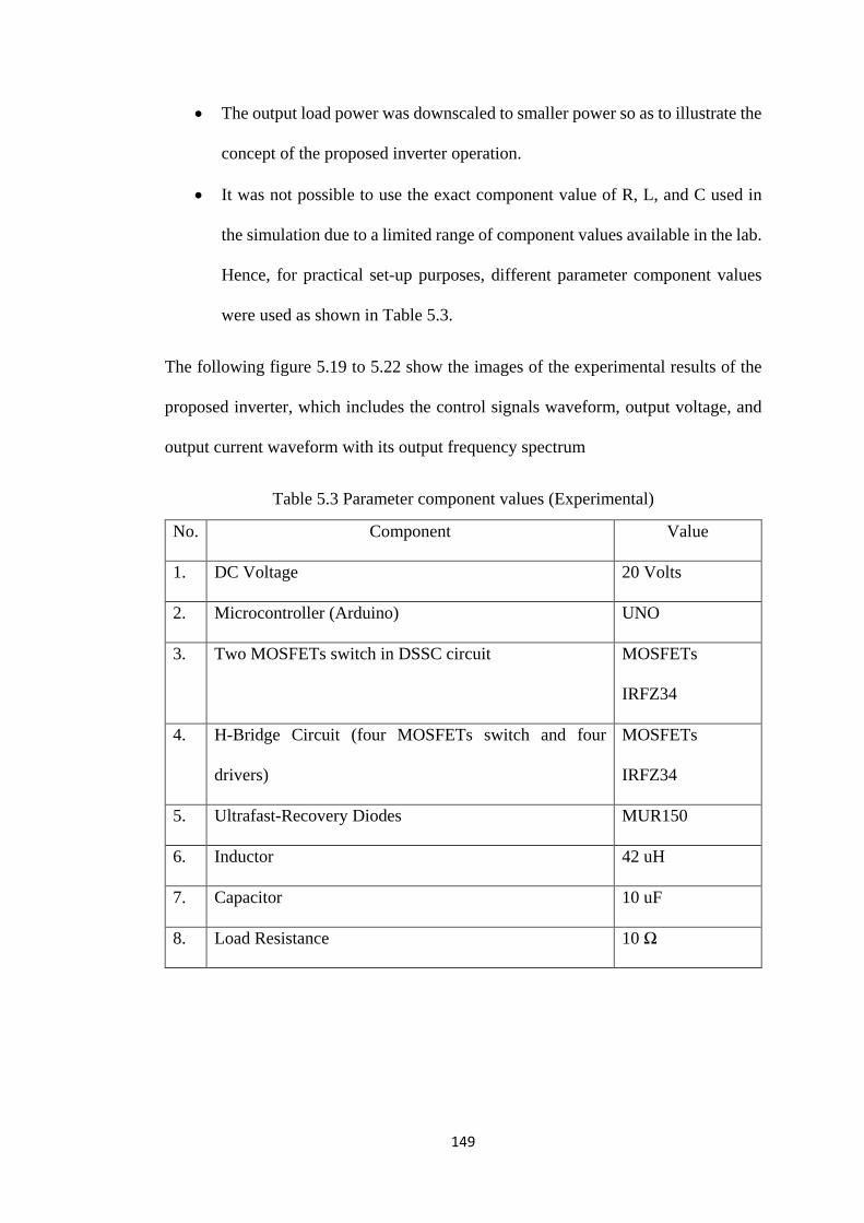
149
• The output load power was downscaled to smaller power so as to illustrate the
concept of the proposed inverter operation.
• It was not possible to use the exact component value of R, L, and C used in
the simulation due to a limited range of component values available in the lab.
Hence, for practical set-up purposes, different parameter component values
were used as shown in Table 5.3.
The following figure 5.19 to 5.22 show the images of the experimental results of the
proposed inverter, which includes the control signals waveform, output voltage, and
output current waveform with its output frequency spectrum
Table 5.3 Parameter component values (Experimental)
No. Component Value
1. DC Voltage 20 Volts
2. Microcontroller (Arduino) UNO
3. Two MOSFETs switch in DSSC circuit MOSFETs
IRFZ34
4. H-Bridge Circuit (four MOSFETs switch and four
drivers)
MOSFETs
IRFZ34
5. Ultrafast-Recovery Diodes MUR150
6. Inductor 42 uH
7. Capacitor 10 uF
8. Load Resistance 10 Ω

150
Figure 5.19 shows two switching pattern signals in anti-parallel waveform used to fed
to the gate terminal of the two power MOSFETs IRFZ34 switches (labelled as S1 and
S2 in circuit diagram Figure 4.2) of the DSSC SCC circuit.
Figure 5.15 Switching pattern control signals
The experiment is conducted to measure the harmonics distortion in proposed inverter
output for operating under two different load conditions. The first case is when a purely
resistive element is applied at output load and the second case is when a highly
inductive element is applied. The following figures show the images of the
experimental results of the voltage and current waveform captured from the
oscilloscope. Figure 5.18 and 5.19 show the output voltage and current waveforms
measured across a purely resistive load of 10 Ω measured result from oscilloscope.
The output voltage is stepped sinusoidal waveform with 15.9 Volts peak-to-peak
output voltage. The measured RMS output voltage Vo is 11.3 Volts. The output
voltage frequency is 50 Hz and the output load power is 12.77 Watt.
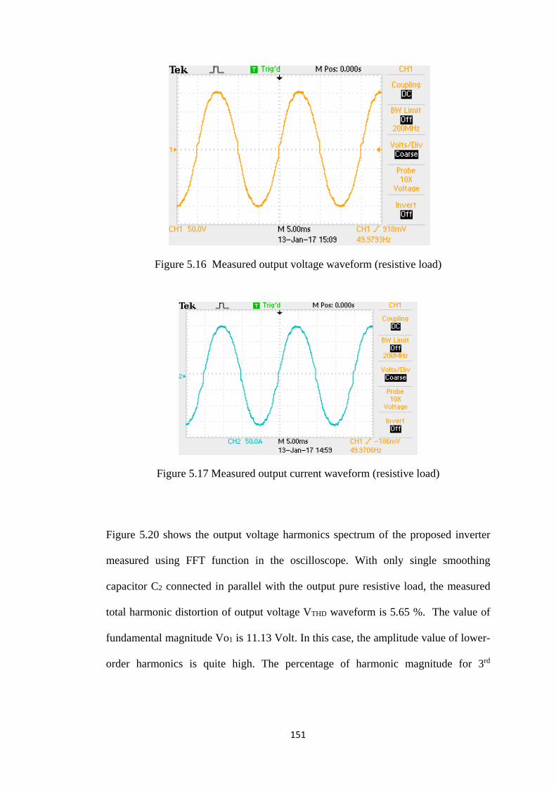
151
Figure 5.16 Measured output voltage waveform (resistive load)
Figure 5.17 Measured output current waveform (resistive load)
Figure 5.20 shows the output voltage harmonics spectrum of the proposed inverter
measured using FFT function in the oscilloscope. With only single smoothing
capacitor C2 connected in parallel with the output pure resistive load, the measured
total harmonic distortion of output voltage VTHD waveform is 5.65 %. The value of
fundamental magnitude Vo1 is 11.13 Volt. In this case, the amplitude value of lower-
order harmonics is quite high. The percentage of harmonic magnitude for 3rd

152
harmonics order is 4.6 % of the fundamental magnitude and other low-order harmonics
are small, less than 1 % of the fundamental magnitude.
Figure 5.18 Measured output voltage harmonics spectrum (resistive load)
Table 5.4 Amplitude of output harmonics (purely resistive load)
Harmonics Order Harmonics magnitude (in %)
3 4.6
5 0.3
7 0.3
9 0.3
11 1.0
13 0.2
Figure 5.21 shows the output voltage waveform across a highly inductive load, Z = 20
+ j 62.8Ω measured result from oscilloscope. The output voltage is a sinusoidal
waveform with 15.9 Volts peak-to-peak output voltage. The measured RMS output
voltage Vo is 11.2 Volts. The output voltage frequency is 50 Hz. The apparent power
is 5 VA.

153
Figure 5.19 Measured output voltage waveform (highly inductive load)
Figure 5.22 shows the output voltage harmonics spectrum of the proposed inverter
measured using FFT function in oscilloscope. The total harmonic distortion of output
voltage VTHD waveform is 3.4 %. The value of fundamental magnitude Vo1 is 11.15
Volt. In this case, the amplitude value of lower-order harmonics is quite high. The
percentage of low-order harmonics is small, less than 2 % of the fundamental
magnitude.
Figure 5.20 Measured output voltage harmonics spectrum (highly inductive load)

154
Table 5.5 Amplitude of output harmonics (highly inductive load)
Harmonics Order Harmonics magnitude (in %)
3 1.9
5 0.3
7 0.6
9 0.6
11 0.4
13 0.2
Figures 5.18 and 5.20 show the proposed inverter output voltage and its output
frequency spectrum which represents the experimental results for operating resistive
load. Only a single smoothing capacitor is used which is connected in parallel to the
load, and the measured THD of the output voltage (VTHD) across pure resistive load
was found to be 5.65 %, which slightly deviated from both the theoretical estimated
results and the simulation results, which are 4.6 % as shown in Figure 5.20. The slight
deviation of experiment result is due to different parameter component value was used
for practical set-up. In addition, the deviation is also due to the assumption to neglect
the inductor resistance, the ohmic resistance of the wires and the bleeder resistance in
capacitor of the proposed/designed inverter circuit. Figure 5.21 and 5.22 shows the
proposed inverter output voltage and its output frequency spectrum which represents
the experimental results for operating highly inductive load. The output voltage and
current waveform is smooth sinusoidal which the measured VTHD was found to be 3.4
% as shown in Figure 5.20. This is because the inductor acts as passive filter.
Therefore, this proposed inverter is ideal to operate with an inductive load. However,

155
it can be seen from the experimental results that the measured THD of the output
voltage waveforms (VTHD) of the proposed inverter shows agreement and validation
with the theoretical concept and estimation calculation results in terms of the THD
performance and operation as presented in Chapter 4, as well as the simulated result.
Practical Comparison amongst DC/AC Inverter Topologies
Table 5.6 shows the comparison amongst different types of DC/AC Inverter circuit;
the traditional three-levels PWM inverter, classical Cascaded H-Bridge Multi-level
inverter (CHB-MLI) circuit topology (Alamri, Darwish 2015), Switched-Capacitor
Boost Multi-Level Inverter (SCB-MLI) circuit topology (Chan and Chau 2007) and
the proposed inverter (A DC/AC Inverter based Switched-Capacitor topology with
reduced number of component). The performance each of topologies are compared in
terms of Total Harmonic Distortion (THD), rating output power and Efficiency as
shown in Table 5.6. These inverter circuit topologies were also compared in terms of
the number of component used for generating thirteen-levels of output voltage. These
circuits are compared in almost same condition for producing a thirteen-levels of
output voltage, rating output power and without use of filter at output.

156
Table 5.6 Experimental comparison between proposed inverter circuit topology and other inverter topologies performance for thirteen-levels output voltage
Topology Number of voltage
levels
m
Vdc
V
Output
Power
Watt
Efficiency THD
%
PWM Inverter
(VSI)
3 60 40 93 % 76
CHB-MLI
13 60 40 93 % 2.01
SCB-MLI
13 60 40 72% 6.3
Proposed Inverter
13 60 40 70% 5.64
Table 5.7 Comparison between proposed inverter and other multi-level inverter topologies in term of components count for thirteen-levels output voltage
Topology DC sources Inductor Capacitor Diode Power
Switch
Total number of
Component PWM
Inverter (VSI)
1 0 0 0 4 4
CHB-MLI
6 0 6 24 24 54
SCB-MLI
1 1 2 3 11 17
Proposed Inverter 1 1 2 1 6 13

157
Discussion
The classical CHB-MLI inverter topology and the recent SCB-MLI inverter
topology can obtain low THD and perform at high efficiency performance as
illustrated in Table 5.6. However, most of these circuit topologies require large number
of components i.e. power switches, diodes and capacitors, and/or isolated DC sources
as illustrated in Table 5.7. The proposed inverter can achieve low THD with less
number of component used in comparison to the CHB-MLI and SCB-MLI topology.
The output voltage shape is highly depending on the component parameter value, type
of semiconductor device used and type of output load. The output voltage is also
sensitive to the parasitic resistance in passive (capacitor and inductor) and active
(Power semiconductor switch) components. The efficiency of the practical
experimentation of the proposed inverter circuit is 70 %. This proposed circuit also
can operate with highly inductive load which can results in smoother output waveform
and lower THD in output voltage and current waveform.
Summary
This chapter presents the simulation and practical hardware implementation of
the proposed inverter circuit. The proposed inverter circuit was designed using the
OrCAD PSPICE simulation package. The simulation shows the ability of the proposed
inverter to generate staircase/multi-level AC output with low THD that can be
achieved without increasing the number of components. The results from the practical,
simulation, and theoretical estimations are consistent. This verified that the proposed
inverter circuit has the ability to generate near AC output voltage waveform with low

158
harmonics distortion using fewer components (power switches and capacitors). The
comparison has been made between the proposed inverter topology and the classical
multi-level inverter topology (Cascaded H-Bridge MLI) in terms of THD performance
and component count. In the final chapter, the conclusions and suggestions of future
works are presented.

159
Chapter 6 Conclusions and Future Work
Conclusions
In this thesis, a new optimum DC/AC inverter based switched-capacitor circuit
with reduced component count was proposed. The following objectives have been
conducted to achieve the research aim where the contribution of knowledge in the field
of DC/AC inverters is described:
1. A critical literature review of DC/AC inverters, conventional PWM, classical,
and newly-evolved multi-level topologies was presented, showing the
advantages and disadvantages of each topology. In addition, the review on the
available voltage boosting technique was presented.
2. The weaknesses of each well-known classical PWM and multi-level DC/AC
inverter topologies covered in the literature were identified. The classical
PWM inverter topologies’ limitations are associated with high total harmonics
distortion and high power losses. Meanwhile, classical multi-level DC/AC
inverter topologies are associated with a large number of power semiconductor
switches, diodes, capacitors, and isolated DC sources. This is to achieve high
output voltage and also to increase the number of levels (high-voltage
resolution) so that low output voltage THD can be obtained. Due to many
advantages, multi-level topology is preferred than traditional three-levels
PWM topology.

160
3. A review on the available voltage boosting technique was conducted. Many
efforts have made to integrate switched-capacitor circuit (SCC) techniques for
boosting voltage. The advantages of this technique can boost voltage and/or
varying voltage with a reduced number of multiple isolated DC input sources.
The decision was made to select SCC as the preferred boosting technique. The
SCC is a cell-based structure which is easy to integrate into other circuit
structures and provides high voltage gain/step-up ability.
4. Switched-capacitor circuit topologies have been examined and other voltage
boosting techniques have been reviewed for voltage gain and varying voltage
ability. Two types of mathematical analysis of the resonant-based DSSC SCC
were carried out. The theoretical relationship between effective capacitance
and duty-cycle, and the relationship between voltage across capacitor and duty
cycle were estimated. It was concluded that with varying duty-cycle the DSSC
circuit varies the capacitance value. It was also found that the voltage across
capacitor varies with varying duty-cycle. By appropriate duty cycle switch
control applied to the associated power switches, this configuration exhibits
voltage gain and regulating voltage abilities. This characteristic lead to the
formation of rectified staircase/multi-level voltage waveform. This
configuration has fewer power switches and capacitors components which may
have less power loss results in an improvement of the efficiency of the system.
5. Other voltage boosting techniques (magnetic couple and multi-stage booster)
were not discussed in detail and selected due to their bulky and inefficient
system. However, they have high-voltage boost voltage ability. The SCC was
found to be suitable as part of a proposed inverter system due to high-voltage
161
gain and varying voltage ability. The other resonant-based SCC configurations
were not discussed in detail due to them being unsuitable for producing multi-
level voltage waveform with duty-cycle controlled applied. The DSDC
configuration does not have varying voltage ability. In SCCC configuration,
short-circuit problems represent a major drawback. It can occur when a switch
is closed while voltage across capacitor has not reached zero. Triplen
configuration may have varying voltage ability. However, it is composed of
many power switches which added to the power losses. Also, high power
dissipation in branch auxiliary resistors may degrade the overall system
efficiency. This represents a major drawback of this configuration.
6. DC/AC inverter-based switched-capacitor circuit topology with reduced
number of components was designed/introduced. The circuit configuration and
modulation control technique were designed, showing the integration of a
DSSC configuration type of SCC with variable duty-cycle control technique
into a single-phase current source inverter (CSI) topology. The principle
operation, design procedure, and analysis were presented.
7. A mathematical derivation was developed for the designed inverter circuit
showing the design procedure leading to the formation of the staircase/multi-
level AC output voltage waveform. During the positive cycle of output
waveform, a rectified near sine (staircase/multi-level) can be first
formed/shaped by controlling the DSSC SCC with variable duty-cycle control
technique in specific switching time pattern. This rectified staircase/multi-level
is then transformed into sinusoidal AC waveform during the negative cycle. To

162
obtain low THD of AC output voltage waveform, the best switching time or
angle is determined by using the Half-Height method. This method is selected
due to simple way to arrange switching angle according to the sine function.
The formation of this rectified waveform is well-accorded to the estimated
relationship (between capacitor voltage and duty-cycle) which was conducted
earlier. Smoother waveform of rectified staircase/multi-level is obtained by
narrowing the pulse width signal applied to control switches. This is achieved
by operating switches of the selected switched-capacitor circuit (resonant-
based DSSC circuit) at high switching frequency. Smooth rectified staircase
waveform can lead to obtaining low THD of AC output voltage of the designed
inverter. Also, only single smoothing capacitor is used at output which act as
output filters. For these reasons, the decision was made for the selected
switched-capacitor circuit with variable duty-cycle controlled to operate at
high switching frequency.
8. The theoretical relationship between voltage THD and switching frequency of
the selected switched-capacitor circuit (resonant-based DSSC circuit) was
estimated. The optimum switching frequency that can yield was identified from
this theoretical estimation. However, switching losses can increase in direct
proportion with switching frequency. The decision of optimum switching
frequency was made by taking into consideration harmonics distortion and
switching losses where both of them must promise. To realise the variable
duty-cycle control technique, the open-loop control logic circuit, which
provides the switching timing control pattern, is presented.

163
9. An investigation has been conducted on commonly used power electronics
simulation software packages for designing and simulating electronics circuits.
OrCAD PSPICE and Psim software packages were identified as two best
alternatives to use. OrCAD PSPICE was found to be superior in providing
accurate modelling for inverter circuit design. PSPICE comprises of libraries
of components according to manufacturer’s specification which can lead to
obtaining realistic simulation result. It also includes an extensive library of
commercial electric components. Hence, OrCAD PSPICE was adopted for
simulating the proposed inverter circuit in this research.
10. The proposed inverter operating under different loads (pure resistive load and
highly inductive load) were verified experimentally. The measured THD of
output voltage across pure resistive load was consistent with the theoretical
estimated results and the simulation results. Meanwhile, the measured THD of
output voltage across highly inductive load was consistent with the simulation
results.
11. The proposed inverter was simulated, showing the full wave rectified near sine
(multi-level) voltage across H-bridge circuit is generated by applying the
control signals (proposed variable duty cycle control technique) fed to the
associated power switch. Also, showing its performance producing near AC
output voltage waveform. The simulation result proved that the new designed
inverter able to generate near sinusoidal AC output voltage with low total
harmonics distortion. It showed an effective way of generating multi-
level/staircase voltage waveform using a reduced number of components

164
(power switches and capacitors) and single DC sources. This was proved
experimentally showing its feasibility in the reduction in the number of
components used compared to VSI PWM inverter and multi-level inverters i.e.
Cascaded H-Bridge Multi-Level Inverter and Switched-Capacitor Boost Multi-
Level Inverter.
12. The simulation result of the new DC/AC inverter topology was discussed from
different views, which is considered as a major contribution to knowledge in
this thesis as follows:
- Contribution of a different way of generating staircase/multi-level voltage
waveform using a DSSC switched-capacitor circuit with variable duty cycle
control technique;
- Contribution to present the new DC/AC inverter-based switched-capacitor
circuit topology with reduced number of components showing its merits
compared to existing multi-level inverter based switched-capacitor circuit
topology.
The system testing and practical implementation were conducted. The simulation
and experimental results are compared which shows good agreement between practical
and simulation results of the new proposed inverter. This will allow researchers to
appreciate the performance of this developed DSSC switched-capacitor circuit with
variable duty cycle control technique by modifying other DC/AC inverter topologies
(multi-stage) for component reduction in future, as well as appreciating the new
designed inverter for use in low power applications.

165
Future Works
The following suggestions for future works are to improve the implementation of
the proposed inverter system.
• An investigation is required to assess the proposed inverter suitability to work
in three-phase AC system high power applications.
• More investigation on Triplen switch configurations of switched-capacitor
circuit with appropriate control technique can be conducted to prove its
suitability to work as a voltage regulator (to the DC input voltage to different
voltage levels). The current rating flow through auxiliary resistor should be
controlled in order to have minimum power dissipation leading to high
efficiency of the overall system.
• More investigation should be done in improving power losses and efficiency
performance of the proposed inverter by adding lossless snubber circuit. The
snubber circuit can be used to limit switch voltage stress dv/dt and reduce
switching losses in switch device. It also provides protection for power switch
devices.
• A closed-loop control system can be implemented to suitably control the
charging capacitor in switched capacitor circuit to achieve more number of
voltage levels in order to improve output voltage resolution.
• An accurate cost analysis of the proposed inverter system at manufacturing
stage can be carried out.

166
References
A. Rahim, K. Chaniago & J. Selvaraj 2011, "Single-Phase Seven-Level Grid-Connected Inverter for Photovoltaic System", IEEE Transactions on Industrial Electronics, vol. 58, no. 6, pp. 2435-2443.
A. Silva 2013, "Advanced DC/AC Inverters: Applications in Renewable Energy (Luo, F.L. and Ye, H.; 2013) [Book News]", IEEE Industrial Electronics Magazine, vol. 7, no. 4, pp. 68-69.
Alamri, B. & Darwish, M. 2014, "Precise modelling of switching and conduction losses in cascaded h-bridge multilevel inverters", Power Engineering Conference (UPEC), 2014 49th International Universities, pp. 1.
Alepuz, S., Busquets-Monge, S., Bordonau, J., Gago, J., Gonzalez, D. & Balcells, J. 2006, "Interfacing Renewable Energy Sources to the Utility Grid Using a Three-Level Inverter", Industrial Electronics, IEEE Transactions on, vol. 53, no. 5, pp. 1504-1511.
Amini & M. Moallem 2017, "A Fault-Diagnosis and Fault-Tolerant Control Scheme for Flying Capacitor Multilevel Inverters", IEEE Transactions on Industrial Electronics, vol. 64, no. 3, pp. 1818-1826.
Anderson & F. Z. Peng 2008, "Four quasi-Z-Source inverters", 2008 IEEE Power Electronics Specialists Conference, pp. 2743.
Arman, M.F. & Darwish, M.K. 2009, "Critical Review of Cascaded H-Bridge Multilevel Inverter Topologies", International Review of Electrical Engineering, vol. 4, no. 5, pp. 703-743.
Axelrod, Y. Berkovich & A. Ioinovici 2005, "A cascade boost-switched-capacitor-converter - two level inverter with an optimized multilevel output waveform", IEEE Transactions on Circuits and Systems I: Regular Papers, vol. 52, no. 12, pp. 2763-2770.
Babaei & S. S. Gowgani 2014, "Hybrid Multilevel Inverter Using Switched Capacitor Units", IEEE Transactions on Industrial Electronics, vol. 61, no. 9, pp. 4614-4621.
Bailu Xiao, Filho, F. & Tolbert, L.M. 2011, "Single-phase cascaded H-bridge multilevel inverter with nonactive power compensation for grid-connected photovoltaic generators", Energy Conversion Congress and Exposition (ECCE), 2011 IEEE, pp. 2733.
Barbosa, P.G., Braga, H.A.C., Rodrigues, M.C.B. & Teixeira, E.C. 2006, "Boost current multilevel inverter and its application on single-phase grid-connected

167
photovoltaic systems", Power Electronics, IEEE Transactions on, vol. 21, no. 4, pp. 1116-1124.
Barzegarkhoo, E. Zamiri, N. Vosoughi, H. M. Kojabadi & L. Chang 2016, "Cascaded multilevel inverter using series connection of novel capacitor-based units with minimum switch count", IET Power Electronics, vol. 9, no. 10, pp. 2060-2075.
Barzegarkhoo, H. M. Kojabadi, E. Zamiry, N. Vosoughi & L. Chang 2016, "Generalized Structure for a Single Phase Switched-Capacitor Multilevel Inverter Using a New Multiple DC Link Producer With Reduced Number of Switches", IEEE Transactions on Power Electronics, vol. 31, no. 8, pp. 5604-5617.
Beig, A.R. & Dekka, A. 2012, "Experimental verification of multilevel inverter-based standalone power supply for low-voltage and low-power applications", Power Electronics, IET, vol. 5, no. 6, pp. 635-643.
Bellar, M.D., Wu, T., Tchamdjou, A., Mahdavi, J. & Ehsani, M. 1998, "A review of soft-switched DC-AC converters", Industry Applications, IEEE Transactions on, vol. 34, no. 4, pp. 847-860.
Bragard, M., Soltau, N., Thomas, S. & De Doncker, R.W. 2010, "The Balance of Renewable Sources and User Demands in Grids: Power Electronics for Modular Battery Energy Storage Systems", Power Electronics, IEEE Transactions on, vol. 25, no. 12, pp. 3049-3056.
C. Marouchos, D. Xenofontos, M. Darwish, M. S. Moghadam & C. Armefti 2014, "The switched capacitor inverter as a MPPT in a photovoltaic application", 2014 49th International Universities Power Engineering Conference (UPEC), pp. 1.
Caceres, R.O. & Barbi, I. 1999, "A boost DC-AC converter: analysis, design, and experimentation", Power Electronics, IEEE Transactions on, vol. 14, no. 1, pp. 134-141.
Calais, M. & Agelidis, V.G. 1998, "Multilevel converters for single-phase grid connected photovoltaic systems-an overview", Industrial Electronics, 1998. Proceedings. ISIE '98. IEEE International Symposium on, pp. 224.
Carrasco, J.M., Franquelo, L.G., Bialasiewicz, J.T., Galvan, E., Guisado, R.C.P., Prats, M.A.M., Leon, J.I. & Moreno-Alfonso, N. 2006, "Power-Electronic Systems for the Grid Integration of Renewable Energy Sources: A Survey", Industrial Electronics, IEEE Transactions on, vol. 53, no. 4, pp. 1002-1016.
Chakraborty and S. Dalapati "A new voltage source inverter realized by controlled capacitor charging", Conf.Rec.International Power Electronic Conference (IPEC 2005), , pp. 2023-2029.

168
Chan, M.S. & Chau, K. 2007, "A new switched-capacitor boost-multilevel inverter using partial charging", Circuits and Systems II: Express Briefs, IEEE Transactions on, vol. 54, no. 12, pp. 1145-1149.
Chellammal, N., Dash, S.S., Velmurugan, V. & Gurram, R. 2012, "Power quality improvement using multilevel inverter as series active filter", Emerging Trends in Science, Engineering and Technology (INCOSET), 2012 International Conference on, pp. 450.
D. Mahale & R. J. Patil 2016, "Comparative analysis of various impedance source inverters", 2016 International Conference on Automatic Control and Dynamic Optimization Techniques (ICACDOT), pp. 207.
Daher, S., Schmid, J. & Antunes, F.L.M. 2008, "Multilevel Inverter Topologies for Stand-Alone PV Systems", Industrial Electronics, IEEE Transactions on, vol. 55, no. 7, pp. 2703-2712.
Darwish, B. R. Alamri & C. Marouchos 2015, "OrCAD vs Matlab Simulink in teaching power electronics", 2015 50th International Universities Power Engineering Conference (UPEC), pp. 1.
De, S., Banerjee, D., Gopakumar, K., Ramchand, R. & Patel, C. 2011, "Multilevel inverters for low-power application", IET Power Electronics, vol. 4, no. 4, pp. 384-392.
Ertl, H., Kolar, J.W. & Zach, F.C. 2002, "A novel multicell DC-AC converter for applications in renewable energy systems", Industrial Electronics, IEEE Transactions on, vol. 49, no. 5, pp. 1048-1057.
Fang Zheng Peng, Jih-Sheng Lai, McKeever, J. & VanCoevering, J. 1995, "A multilevel voltage-source inverter with separate DC sources for static VAr generation", Industry Applications Conference, 1995. Thirtieth IAS Annual Meeting, IAS '95., Conference Record of the 1995 IEEE, pp. 2541.
Floricau & L. Kreindler 2015, "Generalized multilevel inverter topology with stacked coupled inductors", 2015 17th European Conference on Power Electronics and Applications (EPE'15 ECCE-Europe), pp. 1.
Fri, A., El Bachtiri, R. & El Ghzizal, A. 2013, "Comparative study of H-bridge multilevel inverters dedicated to PV", Renewable and Sustainable Energy Conference (IRSEC), 2013 International, pp. 67.
G. Georgakas, P. N. Vovos & N. A. Vovos 2014, "Harmonic Reduction Method for a Single-Phase DC–AC Converter Without an Output Filter", IEEE Transactions on Power Electronics, vol. 29, no. 9, pp. 4624-4632.

169
Georgakas, K.G., Vovos, P.N. & Vovos, N.A. 2014, "Harmonic Reduction Method for a Single-Phase DC–AC Converter Without an Output Filter", Power Electronics, IEEE Transactions on, vol. 29, no. 9, pp. 4624-4632.
Ghasemi, N., Zare, F., Boora, A.A., Ghosh, A., Langton, C. & Blaabjerg, F. 2012, "Harmonic elimination technique for a single-phase multilevel converter with unequal DC link voltage levels", Power Electronics, IET, vol. 5, no. 8, pp. 1418-1429.
He & C. Cheng 2016, "A Flying-Capacitor-Clamped Five-Level Inverter Based on Bridge Modular Switched-Capacitor Topology", IEEE Transactions on Industrial Electronics, vol. 63, no. 12, pp. 7814-7822.
Heldwein, M.L. & Kolar, J.W. 2009, "Impact of EMC filters on the power density of modern three-phase PWM converters", Power Electronics, IEEE Transactions on, vol. 24, no. 6, pp. 1577-1588.
IEEE Recommended Practice and Requirements for Harmonic Control in Electric Power Systems 2014, .
J. C. Rosas-Caro, J. C. Mayo-Maldonado, F. Mancilla-David, A. Valderrabano-Gonzalez & F. Beltran Carbajal 2015, "Single-inductor resonant switched capacitor voltage multiplier with safe commutation", IET Power Electronics, vol. 8, no. 4, pp. 507-516.
J. C. Rosas-Caro, J. M. Ramirez, F. Z. Peng & A. Valderrabano 2010, "A DC-DC multilevel boost converter", IET Power Electronics, vol. 3, no. 1, pp. 129-137.
J. Liu, K. W. E. Cheng & Y. Ye 2014, "A Cascaded Multilevel Inverter Based on Switched-Capacitor for High-Frequency AC Power Distribution System", IEEE Transactions on Power Electronics, vol. 29, no. 8, pp. 4219-4230.
J. Zeng, J. Wu, J. Liu & H. Guo 2017, A Quasi-Resonant Switched-Capacitor Multilevel Inverter With Self-Voltage Balancing for Single-Phase High-Frequency AC Microgrids.
Jiang & T. A. Lipo 1998, "Switching angles and DC link voltages optimization for multilevel cascade inverters", 1998 International Conference on Power Electronic Drives and Energy Systems for Industrial Growth, 1998. Proceedings., pp. 56.
Jih-Sheng Lai & Fang Zheng Peng 1995, "Multilevel converters-a new breed of power converters", Industry Applications Conference, 1995. Thirtieth IAS Annual Meeting, IAS '95., Conference Record of the 1995 IEEE, pp. 2348.
Jing Huang & K. Corzine 2004, "Extended operation of flying capacitor multilevel inverters", Conference Record of the 2004 IEEE Industry Applications Conference, 2004. 39th IAS Annual Meeting., pp. 813.

170
K. K. Gupta, A. Ranjan, P. Bhatnagar, L. K. Sahu & S. Jain 2016, "Multilevel Inverter Topologies With Reduced Device Count: A Review", IEEE Transactions on Power Electronics, vol. 31, no. 1, pp. 135-151.
K. Peter & V. Agarwal 2017, "Photovoltaic Module-Integrated Stand-alone Single-Stage Switched Capacitor Inverter with Maximum Power Point Tracking", IEEE Transactions on Power Electronics, vol. 32, no. 5, pp. 3571-3584.
K. Sano & H. Fujita 2008, "Voltage-Balancing Circuit Based on a Resonant Switched-Capacitor Converter for Multilevel Inverters", IEEE Transactions on Industry Applications, vol. 44, no. 6, pp. 1768-1776.
Lin, B.-. & Hung, T.-. 2002, "Analysis and implementation of a single-phase multilevel inverter for power quality improvement", Industrial Electronics, 2002. ISIE 2002. Proceedings of the 2002 IEEE International Symposium on, pp. 1235.
M. Darwish & C. Marouchos 2014, "Modular OrCAD simulation approach in teaching power electronics", 2014 49th International Universities Power Engineering Conference (UPEC), pp. 1.
M. Darwish & P. Mehta 1990, "Switched-capacitor technique for power electronic applications", 21st Annual IEEE Conference on Power Electronics Specialists, pp. 698.
M. Darwish, P. Mehta & T. Thomson 1988, "Variable characteristic filters", Third International Conference on Power Electronics and Variable-Speed Drives, pp. 424.
M. F. Arman, C. C. Marouchos & M. K. Darwish 2012, "Self-tuning output passive-filter for low power DC/AC inverters", 2012 47th International Universities Power Engineering Conference (UPEC), pp. 1.
M. Forouzesh, Y. P. Siwakoti, S. A. Gorji, F. Blaabjerg & B. Lehman 2017, Step-Up DC–DC Converters: A Comprehensive Review of Voltage Boosting Techniques, Topologies, and Applications.
M. H. H. Rozlan, M. K. Darwish, A. Sallama & M. Khodapanah 2015, "Low loss inverter circuit based on buck and boost topology", 2015 50th International Universities Power Engineering Conference (UPEC), pp. 1.
Machado Martins, J. Antenor Pomilio & S. Buso 2001, "A single-phase low-frequency commutation inverter for renewables", Industrial Electronics Society, 2001. IECON '01. The 27th Annual Conference of the IEEE, pp. 1976.
Madouh, J., Ahmed, N.A. & Al-Kandari, A.M. 2012, "Advanced power conditioner using sinewave modulated buck–boost converter cascaded polarity

171
changing inverter", International Journal of Electrical Power & Energy Systems, vol. 43, no. 1, pp. 280-289.
Malad, C.P. & Rao, K.U. 2012, "Simulation of a buck-boost single phase voltage source inverter for distribution generation systems", Int.J.Modern Eng.Res, vol. 2, no. 5, pp. 3628-3632.
Malathy, S., Ramaprabha, R. & Mathur, B.L. 2013, "Asymmetrical multilevel inverters for partially shaded PV systems", Circuits, Power and Computing Technologies (ICCPCT), 2013 International Conference on, pp. 579.
Marchesoni, M., Mazzucchelli, M. & Tenconi, S. 1990, "A nonconventional power converter for plasma stabilization", Power Electronics, IEEE Transactions on, vol. 5, no. 2, pp. 212-219.
Marouchos, M. Darwish, M. S. Moghadam & M. Georgiou 2015, "A new switched capacitor inverter for stand alone photovoltaic applications", 2015 50th International Universities Power Engineering Conference (UPEC), pp. 1.
Martins, G.M., Pomilio, J.A. & Buso, S. 2001, "A single-phase low-frequency commutation inverter for renewables", Industrial Electronics Society, 2001. IECON '01. The 27th Annual Conference of the IEEE, pp. 1976.
Mecke, R. 2011, "Multilevel NPC inverter for low-voltage applications", Power Electronics and Applications (EPE 2011), Proceedings of the 2011-14th European Conference on, pp. 1.
Mellitt & M. H. Rashid 1974, "Analysis of d.c. chopper circuits by computer-based piecewise-linear technique", Electrical Engineers, Proceedings of the Institution of, vol. 121, no. 3, pp. 173-178.
Moghadam, M., Darwish, M. & Marouchos, C. 2013, "A simple drive induction motor based on buck/boost inverter topology", Power Engineering Conference (UPEC), 2013 48th International Universities'IEEE, , pp. 1.
Moghadam, M.S. & Darwish, M. 2012, "A buck/boost based Multilevel inverter topology for UPEC2012 conference proceeding", Universities Power Engineering Conference (UPEC), 2012 47th International, pp. 1.
Moir 1999, "More-electric aircraft-system considerations", IEE Colloquium on Electrical Machines and Systems for the More Electric Aircraft (Ref. No. 1999/180), pp. 10/1.
Mosazadeh, S.Y., Fathi, S.H. & Radmanesh, H. 2012, "New high frequency switching method of cascaded multilevel inverters in PV application", Power Engineering and Renewable Energy (ICPERE), 2012 International Conference on, pp. 1.

172
Nabae, I. Takahashi & H. Akagi 1981, "A New Neutral-Point-Clamped PWM Inverter", IEEE Transactions on Industry Applications, vol. IA-17, no. 5, pp. 518-523.
Panagis, P., Stergiopoulos, F., Marabeas, P. & Manias, S. 2008, "Comparison of state of the art multilevel inverters", Power Electronics Specialists Conference, 2008. PESC 2008. IEEE, pp. 4296.
Pereda, J. & Dixon, J. 2013, "Cascaded Multilevel Converters: Optimal Asymmetries and Floating Capacitor Control", Industrial Electronics, IEEE Transactions on, vol. 60, no. 11, pp. 4784-4793.
R. Beig & A. Dekka 2012, "Experimental verification of multilevel inverter-based standalone power supply for low-voltage and low-power applications", IET Power Electronics, vol. 5, no. 6, pp. 635-643.
R. de Souza Santos, T. B. Lazzarin & I. Barbi 2015, "A new half-bridge Hybrid Switched-Capacitor inverter", 2015 IEEE 13th Brazilian Power Electronics Conference and 1st Southern Power Electronics Conference (COBEP/SPEC), pp. 1.
R. Lai, F. Wang, R. Burgos, Y. Pei, D. Boroyevich, B. Wang, T. A. Lipo, V. D. Immanuel & K. J. Karimi 2008, "A Systematic Topology Evaluation Methodology for High-Density Three-Phase PWM AC-AC Converters", IEEE Transactions on Power Electronics, vol. 23, no. 6, pp. 2665-2680.
Rodriguez, J., Jih-Sheng Lai & Fang Zheng Peng 2002, "Multilevel inverters: a survey of topologies, controls, and applications", Industrial Electronics, IEEE Transactions on, vol. 49, no. 4, pp. 724-738.
S. De, D. Banerjee, K. S. Kumar, K. Gopakumar, R. Ramchand & C. Patel 2011, "Multilevel inverters for low-power application", IET Power Electronics, vol. 4, no. 4, pp. 384-392.
Sabahi, M., Marami Iranaq, A.R.M., Bahrami, K.M., Bahrami, K.M. & Sharifian, M.B.B. 2011, "Harmonics elimination in a multilevel inverter with unequal DC sources using genetic algorithm", Electrical Machines and Systems (ICEMS), 2011 International Conference on, pp. 1.
Sanjeev, P. & Jain, S. 2013, "Analysis of conduction and switching losses in two level inverter for low power applications", India Conference (INDICON), 2013 Annual IEEE, pp. 1.
Shamil, M., Darwish, M. & Marouchos, C. 2012, "Single phase Multi level inverter with desire harmonics", Universities Power Engineering Conference (UPEC), 2012 47th International, pp. 1.

173
Shinohara, H., Kimoto, K., Itami, T., Ambou, T., Okado, C., Nakajima, K., Hojo, S., Owada, K., Kuniyoshi, M. & Sato, Y. 1994, "Development of a residential use, utility interactive PV inverter with isolation transformer-less circuit-development aspects", Photovoltaic Energy Conversion, 1994., Conference Record of the Twenty Fourth. IEEE Photovoltaic Specialists Conference - 1994, 1994 IEEE First World Conference on, pp. 1216.
Shukla, A., Ghosh, A. & Joshi, A. 2012, "Control of dc capacitor voltages in diode-clamped multilevel inverter using bidirectional buck-boost choppers", Power Electronics, IET, vol. 5, no. 9, pp. 1723-1732.
Silva, F. 2013, "Advanced DC/AC Inverters: Applications in Renewable Energy (Luo, F.L. and Ye, H.; 2013) [Book News]", Industrial Electronics Magazine, IEEE, vol. 7, no. 4, pp. 68-69.
Taghvaie, J. Adabi & M. Rezanejad 2016, "Circuit Topology and Operation of a Step-Up Multilevel Inverter With a Single DC Source", IEEE Transactions on Industrial Electronics, vol. 63, no. 11, pp. 6643-6652.
Tolbert, L.M. & Peng, F.Z. 2000, "Multilevel converters as a utility interface for renewable energy systems", Power Engineering Society Summer Meeting, 2000. IEEE, pp. 1271.
Tsunoda, Y. Hinago & H. Koizumi 2012, "A grid connected inverter with switched capacitor inverter using series/parallel conversion", 2012 15th International Power Electronics and Motion Control Conference (EPE/PEMC), pp. LS7c.4-1.
Van der Broeck, H. & Miller, M. 1995, "Harmonics in DC to AC converters of single phase uninterruptible power supplies", Telecommunications Energy Conference, 1995. INTELEC '95., 17th International, pp. 653.
Velmurugan, V., Chellammal, N. & Abirami, R. 2013, "Power quality conditioning using Hybrid multilevel inverter as UPQC", Circuits, Power and Computing Technologies (ICCPCT), 2013 International Conference on, pp. 43.
X. Sun, B. Wang, Y. Zhou, W. Wang, H. Du & Z. Lu 2016, "A Single DC Source Cascaded Seven-Level Inverter Integrating Switched-Capacitor Techniques", IEEE Transactions on Industrial Electronics, vol. 63, no. 11, pp. 7184-7194.
Xue, Y., Chang, L., Kjaer, S.B., Bordonau, J. & Shimizu, T. 2004, "Topologies of single-phase inverters for small distributed power generators: an overview", Power Electronics, IEEE Transactions on, vol. 19, no. 5, pp. 1305-1314.
Y. Hinago & H. Koizumi 2012, "A Switched-Capacitor Inverter Using Series/Parallel Conversion With Inductive Load", IEEE Transactions on Industrial Electronics, vol. 59, no. 2, pp. 878-887.

174
Y. Ye, K. W. E. Cheng, J. Liu & K. Ding 2014, "A Step-Up Switched-Capacitor Multilevel Inverter With Self-Voltage Balancing", IEEE Transactions on Industrial Electronics, vol. 61, no. 12, pp. 6672-6680.
Z. Bai, Z. Zhang & Y. Zhang 2007, "A Generalized Three-Phase Multilevel Current Source Inverter with Carrier Phase-Shifted SPWM", 2007 IEEE Power Electronics Specialists Conference, pp. 2055.
Zamiri, N. Vosoughi, S. H. Hosseini, R. Barzegarkhoo & M. Sabahi 2016, "A New Cascaded Switched-Capacitor Multilevel Inverter Based on Improved Series–Parallel Conversion With Less Number of Components", IEEE Transactions on Industrial Electronics, vol. 63, no. 6, pp. 3582-3594.
Zhong Du, Ozpineci, B., Tolbert, L.M. & Chiasson, J.N. 2009, "DC–AC Cascaded H-Bridge Multilevel Boost Inverter With No Inductors for Electric/Hybrid Electric Vehicle Applications", Industry Applications, IEEE Transactions on, vol. 45, no. 3, pp. 963-970.

175
Appendix A

176
Arduino C-language Program Code: Switching Control Pattern Generation
The following Arduino C-language Program Code shows the generation of the
switching pattern pulses signals (S1 and S2) applied to the two power MOSFETs
switches (S1) and (S2) in Double Switches Single Capacitor (DSSC) circuit. Each of
power semiconductor MOSFETs used in the proposed circuit are controlled by the
microcontroller (Arduino Uno). The control signals (S1 and S2) are in anti-parallel
operation (S1 is HIGH(ON) and S2 is LOW(OFF)).
const int OutPin1 = 11; // control signals(S1)
const int OutPin2 = 10; // control signal (S2)
void setup()
pinMode(OutPin1,OUTPUT);
pinMode(OutPin2,OUTPUT);
void loop()
digitalWrite(11, HIGH); //
digitalWrite(10, LOW); //
delayMicroseconds(10000); // On for 10ms
digitalWrite(11, LOW); //
digitalWrite(10, HIGH); //
delayMicroseconds(10000); // On for 10ms

177
while(digitalRead(OutPin1) == HIGH)//while pin 11 high, perform looping
for (int i = 1; i <= 4; i++) //repeat 4 cycles
// DutyCycle(D)=95% or D=0.95
digitalWrite(13, LOW); //
digitalWrite(12, HIGH); //
delayMicroseconds(19); // On for 19us
digitalWrite(13, HIGH); //
digitalWrite(12, LOW); //
delayMicroseconds(1); // Off for 1 microseconds
for (int i = 1; i <= 3; i++) //repeat 3 cycles
// DutyCycle(D)=85% or D=0.85
digitalWrite(13, LOW); //
digitalWrite(12, HIGH); //
delayMicroseconds(17); // On for 17us
digitalWrite(13, HIGH); //
digitalWrite(12, LOW); //
delayMicroseconds(3); // Off for 3 microseconds
for (int i = 1; i <= 3; i++) //repeat 3 cycles

178
// DutyCycle(D)=75% or D=0.75
digitalWrite(13, LOW); //
digitalWrite(12, HIGH); //
delayMicroseconds(15); // On for 15us
digitalWrite(13, HIGH); //
digitalWrite(12, LOW); //
delayMicroseconds(5); // Off for 5 microseconds
for (int i = 1; i <= 4; i++) //repeat 3 cycles
// DutyCycle(D)=65% or D=0.65
digitalWrite(13, LOW); //
digitalWrite(12, HIGH); //
delayMicroseconds(13); // On for 15us
digitalWrite(13, HIGH); //
digitalWrite(12, LOW); //
delayMicroseconds(7); // Off for 5 microseconds
for (int i = 1; i <= 4; i++) //repeat 3 cycles
// DutyCycle(D)=55% or D=0.55
digitalWrite(13, LOW); //
digitalWrite(12, HIGH); //
delayMicroseconds(11); // On for 15us

179
digitalWrite(13, HIGH); //
digitalWrite(12, LOW); //
delayMicroseconds(9); // Off for 5 microseconds
for (int i = 1; i <= 14; i++) //repeat 7 cycles
// DutyCycle(D)=40% or D=0.4
digitalWrite(13, LOW); //
digitalWrite(12, HIGH); //
delayMicroseconds(8); //
digitalWrite(13, HIGH); //
digitalWrite(12, LOW); //
delayMicroseconds(12); //
for (int i = 1; i <= 4; i++) //repeat 3 cycles
// DutyCycle(D)=55% or D=0.55
digitalWrite(13, LOW); //
digitalWrite(12, HIGH); //
delayMicroseconds(11); // On for 15us
digitalWrite(13, HIGH); //
digitalWrite(12, LOW); //
delayMicroseconds(9); // Off for 5 microseconds
for (int i = 1; i <= 4; i++) //repeat 3 cycles

180
// DutyCycle(D)=65% or D=0.65
digitalWrite(13, LOW); //
digitalWrite(12, HIGH); //
delayMicroseconds(13); // On for 15us
digitalWrite(13, HIGH); //
digitalWrite(12, LOW); //
delayMicroseconds(7); // Off for 5 microseconds
for (int i = 1; i <= 3; i++) //repeat 3 cycles
// DutyCycle(D)=75% or D=0.75
digitalWrite(13, LOW); //
digitalWrite(12, HIGH); //
delayMicroseconds(15); // On for 15us
digitalWrite(13, HIGH); //
digitalWrite(12, LOW); //
delayMicroseconds(5); // Off for 5 microseconds
for (int i = 1; i <= 3; i++) //repeat 3 cycles
// DutyCycle(D)=85% or D=0.85
digitalWrite(13, LOW); //
digitalWrite(12, HIGH); //
delayMicroseconds(17); // On for 17us

181
digitalWrite(13, HIGH); //
digitalWrite(12, LOW); //
delayMicroseconds(3); // Off for 3 microseconds
for (int i = 1; i <= 4; i++) //repeat 4 cycles
// DutyCycle(D)=95% or D=0.95
digitalWrite(13, LOW); //
digitalWrite(12, HIGH); //
delayMicroseconds(19); // On for 19us
digitalWrite(13, HIGH); //
digitalWrite(12, LOW); //
delayMicroseconds(1); // Off for 1 microseconds

182
Appendix B

183
List of Publications
M. H. H. Rozlan, M. K. Darwish, A. Sallama & M. Khodapanah 2015, "Low loss
inverter circuit based on buck and boost topology", 2015 50th International
Universities Power Engineering Conference (UPEC), pp. 1.
M. Khodapanah, A. F. Zobaa, M. H. H. Rozlan, & M. Abbod 2015, "Monitoring of
power factor for induction machines using estimation techniques", 2015 50th
International Universities Power Engineering Conference (UPEC), pp. 1.
M. H. H. Rozlan, M. K. Darwish, "A components reduction in switched-capacitor
multilevel inverters topologies using resonant switched-capacitor circuit technique",
International Review of Electrical Engineering, Submitted in May 2017.