dcc booster module (kit 59) building instructions issue 1 ... · these are the building...
TRANSCRIPT
DCC Booster Module (Kit 59)Building Instructions Issue 1 March 2012
© Martin Perry – March 2012 Page 1 of 10 59DCCBooster BuildIns1.doc
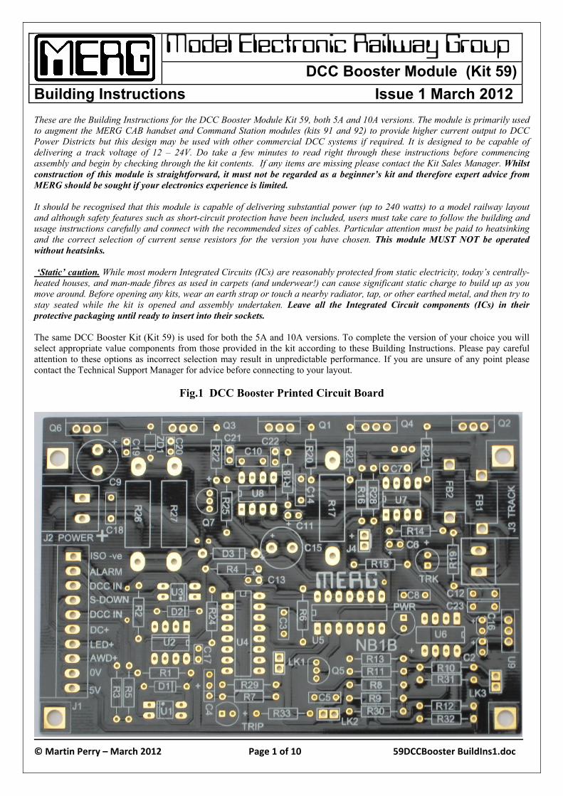
These are the Building Instructions for the DCC Booster Module Kit 59, both 5A and 10A versions. The module is primarily used to augment the MERG CAB handset and Command Station modules (kits 91 and 92) to provide higher current output to DCC Power Districts but this design may be used with other commercial DCC systems if required. It is designed to be capable of delivering a track voltage of 12 – 24V. Do take a few minutes to read right through these instructions before commencing assembly and begin by checking through the kit contents. If any items are missing please contact the Kit Sales Manager. Whilst construction of this module is straightforward, it must not be regarded as a beginner’s kit and therefore expert advice from MERG should be sought if your electronics experience is limited. It should be recognised that this module is capable of delivering substantial power (up to 240 watts) to a model railway layout and although safety features such as short-circuit protection have been included, users must take care to follow the building and usage instructions carefully and connect with the recommended sizes of cables. Particular attention must be paid to heatsinking and the correct selection of current sense resistors for the version you have chosen. This module MUST NOT be operated without heatsinks. ‘Static’ caution. While most modern Integrated Circuits (ICs) are reasonably protected from static electricity, today’s centrally-heated houses, and man-made fibres as used in carpets (and underwear!) can cause significant static charge to build up as you move around. Before opening any kits, wear an earth strap or touch a nearby radiator, tap, or other earthed metal, and then try to stay seated while the kit is opened and assembly undertaken. Leave all the Integrated Circuit components (ICs) in their protective packaging until ready to insert into their sockets. The same DCC Booster Kit (Kit 59) is used for both the 5A and 10A versions. To complete the version of your choice you will select appropriate value components from those provided in the kit according to these Building Instructions. Please pay careful attention to these options as incorrect selection may result in unpredictable performance. If you are unsure of any point please contact the Technical Support Manager for advice before connecting to your layout.
Fig.1 DCC Booster Printed Circuit Board
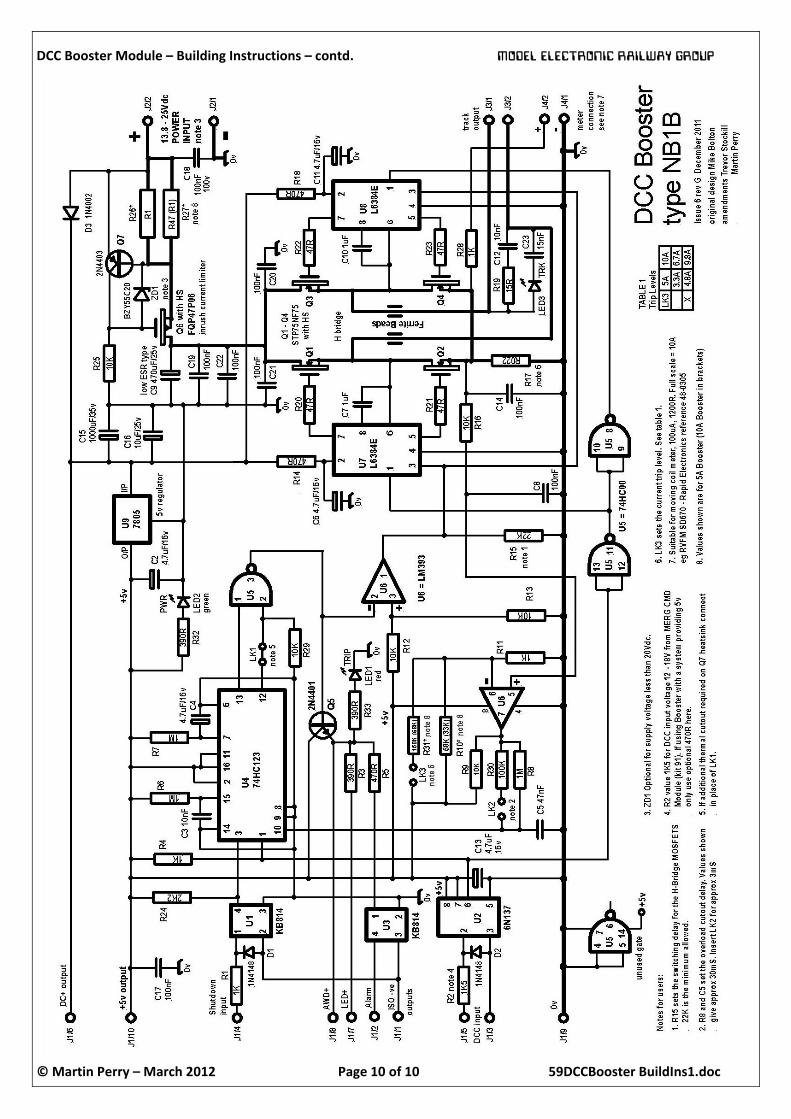
DCC Booster Module – Building Instructions – contd. MODEL ELECTRONIC RAILWAY GROUP
© Martin Perry – March 2012 Page 2 of 10 59DCCBooster BuildIns1.doc
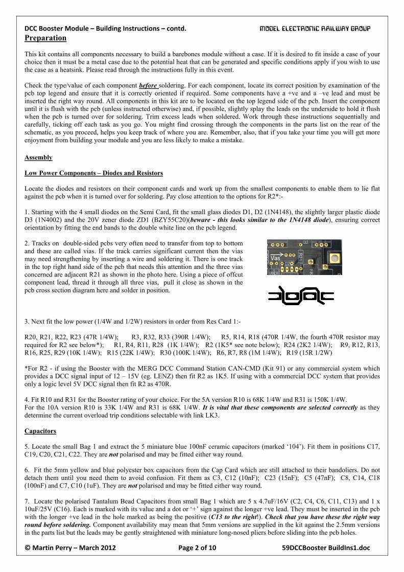
Preparation This kit contains all components necessary to build a barebones module without a case. If it is desired to fit inside a case of your choice then it must be a metal case due to the potential heat that can be generated and specific conditions apply if you wish to use the case as a heatsink. Please read through the instructions fully in this event. Check the type/value of each component before soldering. For each component, locate its correct position by examination of the pcb top legend and ensure that it is correctly oriented if required. Some components have a +ve and a –ve lead and must be inserted the right way round. All components in this kit are to be located on the top legend side of the pcb. Insert the component until it is flush with the pcb (unless instructed otherwise) and, if possible, slightly splay the leads on the underside to hold it flush when the pcb is turned over for soldering. Trim excess leads when soldered. Work through these instructions sequentially and carefully, ticking off each task as you go. You might find crossing through the components in the parts list on the rear of the schematic, as you proceed, helps you keep track of where you are. Remember, also, that if you take your time you will get more enjoyment from building your module and you are less likely to make a mistake. Assembly Low Power Components – Diodes and Resistors Locate the diodes and resistors on their component cards and work up from the smallest components to enable them to lie flat against the pcb when it is turned over for soldering. Pay close attention to the options for R2*:- 1. Starting with the 4 small diodes on the Semi Card, fit the small glass diodes D1, D2 (1N4148), the slightly larger plastic diode D3 (1N4002) and the 20V zener diode ZD1 (BZY55C20)(beware - this looks similar to the 1N4148 diode), ensuring correct orientation by fitting the end bands to the double white line on the pcb legend. 2. Tracks on double-sided pcbs very often need to transfer from top to bottom and these are called vias. If the track carries significant current then the vias may need strengthening by inserting a wire and soldering it. There is one track in the top right hand side of the pcb that needs this attention and the three vias concerned are adjacent R21 as shown in the photo here. Using a piece of offcut component lead, thread it through all three vias, pull it close as shown in the pcb cross section diagram here and solder in position.
3. Next fit the low power (1/4W and 1/2W) resistors in order from Res Card 1:- R20, R21, R22, R23 (47R 1/4W); R3, R32, R33 (390R 1/4W); R5, R14, R18 (470R 1/4W, the fourth 470R resistor may required for R2 see below*); R1, R4, R11, R28 (1K 1/4W); R2 (1K5* see note below); R24 (2K2 1/4W); R9, R12, R13, R16, R25, R29 (10K 1/4W); R15 (22K 1/4W); R30 (100K 1/4W); R6, R7, R8 (1M 1/4W); R19 (15R 1/2W) *For R2 - if using the Booster with the MERG DCC Command Station CAN-CMD (Kit 91) or any commercial system which provides a DCC signal input of 12 – 15V (eg. LENZ) then fit R2 as 1K5. If using with a commercial DCC system that provides only a logic level 5V DCC signal then fit R2 as 470R. 4. Fit R10 and R31 for the Booster rating of your choice. For the 5A version R10 is 68K 1/4W and R31 is 150K 1/4W. For the 10A version R10 is 33K 1/4W and R31 is 68K 1/4W. It is vital that these components are selected correctly as they determine the current overload trip conditions selectable with link LK3. Capacitors 5. Locate the small Bag 1 and extract the 5 miniature blue 100nF ceramic capacitors (marked ‘104’). Fit them in positions C17, C19, C20, C21, C22. They are not polarised and may be fitted either way round. 6. Fit the 5mm yellow and blue polyester box capacitors from the Cap Card which are still attached to their bandoliers. Do not detach them until you need them to avoid confusion. Fit them as C3, C12 (10nF); C23 (15nF); C5 (47nF); C8, C14, C18 (100nF) and C7, C10 (1uF). They are not polarised and may be fitted either way round. 7. Locate the polarised Tantalum Bead Capacitors from small Bag 1 which are 5 x 4.7uF/16V (C2, C4, C6, C11, C13) and 1 x 10uF/25V (C16). Each is marked with its value and a dot or ‘+’ sign against the longer +ve lead. They must be inserted in the pcb with the longer +ve lead in the hole marked as being the positive (C13 to the right!). Check that you have these the right way round before soldering. Component availability may mean that 5mm versions are supplied in the kit against the 2.5mm versions in the parts list but the leads may be gently straightened with miniature long-nosed pliers before sliding into the pcb holes.
DCC Booster Module – Building Instructions – contd. MODEL ELECTRONIC RAILWAY GROUP
© Martin Perry – March 2012 Page 3 of 10 59DCCBooster BuildIns1.doc
DIL Opto-Isolators and DIL Sockets 8. Locate the two 4-pin DIL KB814 opto-isolators from Bag 2 which are to be inserted directly into the pcb in positions U1 and U3. It is vital to install these correctly oriented where pin 1, top left of the IC, is on the chamfered side. Therefore when looking at the pcb the chamfer on U1 must be left-facing and that on U3 right facing (pin 1 is the square pad). Insert the IC into the pcb and bend over 2 diagonal corner pins to hold it in position. Solder the other 2 diagonal corner pins (the ones NOT bent over) and right the pcb to check you have indeed got the orientation correct (it’s a lot easier to extract an IC that way, if you get it wrong). If OK solder the remaining pins. 9. Fit the 6 DIL IC sockets from the DIL tube, for U2, U6, U7, U8 (8-pin); U5 (14 pin) and U4 (16-pin) using the same procedure as for the opto-isolators in paragraph 7 above. The ‘bite’ on the socket must align with that on the pcb legend. For each socket, insert into the pcb, slightly splay 2 diagonal corner pins, right the pcb to check you have it inserted correctly and solder 2 diagonal corner pins not splayed. If satisfied, solder the remaining pins. For any IC or DIL socket it is good practice to solder diagonally opposite pins to spread the heat effect on the component. Do not insert the DIL ICs at this stage Current Sense Resistors R26 and R27 – Res Card 2 10. Locate one of the high wattage resistors (0.1R 3W) for R26 which is common to both 5A and 10A versions. This resistor may get warm during normal operation so it shall be installed so that it sits slightly proud of the pcb. Bend its leads at right angles at the appropriate positions so that the component easily fits through the pcb pads provided and turn the pcb over, face down, ready for soldering. The resistor should drop slightly onto the bench surface leaving a small gap between itself and the pcb. Solder in this position. 11. If building the 5A version, R27 may be left vacant but, depending upon the PSU used, it might be required to establish a slightly higher current limiting threshold, eg if using MERG kit 774 15v 6A SMPS. If so, fit the 0.47R 1W resistor as R27, using the same method as for R26. Otherwise leave it out. 12. If building the 10A version fit the second 0.1R 3W resistor as R27 using the same method as for R26. Do not fit this resistor as R27 if building the 5A version. Links and Terminal Blocks from Bag 1 13. Locate the 6 pin 2.54mm pcb header plug which you must gently cut into 3 x 2 pin headers for LK1, LK2, LK3 with a small pair of cutters or a sharp pair of nail scissors. These headers shatter easily if not careful. Insert into position on the pcb with the longer pins upright, when looking at the pcb top, and solder in position one at a time. Try to ensure that the header is firm against the pcb or else it will look crooked when viewed from the top. Sometimes it is useful to place a jumper link over the longer component side pins. 14. The Booster allows for the optional attachment of a moving coil 100uA 1200ohm panel meter (not supplied in the kit) to provide a continuous measure of the current drawn from the attached track. This connects at J4. If opting for this facility then fit the 2 way yellow Molex-type 2.54mm header in position J4 so that the locking pad is adjacent to C6. A 2 way Molex-type shell and 2 crimp terminals are supplied to attach to your meter leads, one of which is +ve (connects closest to the MOSFETS) and one of which is –ve. Do get these the correct way round or else the meter needle will swing in the wrong direction and may damage the meter mechanism. When connected the meter would read 10A at full scale deflection so 50uA = 5A and 100uA = 10A. A suitable meter would be the RVFM SD670 available from Rapid Electronics ref 48-0305. For other meters of different resistance the value of R28 might need to be adjusted to render a full scale reading at 10A. 15. Locate the 5 2-way 3.5mm (smaller) terminal blocks which you will slide together to make 1 x 10way block (J1). They have small ribs and grooves on the mating edges which must be properly engaged to enable the resultant block to sit correctly on the pcb. Insert in the pcb ensuring that the cable entry holes face the pcb edge. Solder one pin at each end and right the pcb to check you have it the right way round. Solder the remaining pins. 16. Similarly fit the 2 larger 5mm terminal blocks (J2 and J3) with the cable entry holes facing the pcb edge. Major Components 17. Locate the large R022 resistor (R17) from Res Card 2. As for resistors R26 and R27 in paragraph 9. above, it should be installed slightly proud of the pcb as it may get warm in normal use. Bend the leads at right angles at the appropriate positions so that the resistor easily fits in the space provided and turn the pcb over, face down, ready for soldering. The resistor should drop slightly onto the bench surface leaving a small gap between itself and the pcb. Solder in this position. 18. Insert the red (TRIP), green (PWR) and white bi-coloured (TRK) Light Emitting Diodes from Bag 1 in the appropriate places on the pcb such that the longer +ve lead (the one opposite to the flat in the LED rim) is in the +ve hole. Slightly splay the leads to
DCC Booster Module – Building Instructions – contd. MODEL ELECTRONIC RAILWAY GROUP
© Martin Perry – March 2012 Page 4 of 10 59DCCBooster BuildIns1.doc
hold them in position and right the pcb to check you have them the right way round. Straighten them up, if standing crooked, and solder in position. 19. Locate the two small, black, plastic-bodied transistors, Q5 (2N4401) and Q7 (2N4403) from the Semi Card. One at a time insert their legs into the appropriate places on the pcb so that the transistor body matches that on the pcb legend. This ensures correct orientation. It is not necessary to push the body right up against the pcb but it’s neater if they stand up straight. Slightly splay the outer legs only to hold them in position and then right the pcb to check that you have them in the right position (the Booster will not work if you have them switched!). When satisfied, solder in position. 20. Cut the short 50mm section of grey or black insulated wire into two 25mm sections which will be used to mount the two 7mm x 8mm ferrite beads supplied in hardware Bag 3. Strip the insulation from about 6mm of each end of both leaving a central section of insulation about 12mm long. Thread one through one of the ferrite beads and pass the ends through the holes in the pcb for FB1. Pull tight so that the ferrite bead is held firmly against the pcb. Solder in position. Repeat for FB2. It is important that neither bead makes electrical contact with the securing wire or each other. 21. Insert the polarised Low ESR Electrolytic Capacitor C9 (470uF/25V) from Bag 2 into the pcb so that it is correctly oriented, the longer +ve lead (the one opposite the lighter stripe on the capacitor case) goes in the +ve hole. Insert it as far as it will go and slightly splay the leads to hold it in position. Right the pcb to check you have it the right way round before soldering. 22. Insert the TO220 7805 regulator IC (U9) into the pcb so that its metal tab faces the pcb edge and aligns with the pcb legend. Solder in position. This does not need a heatsink in normal operation but may do if you are planning on powering significant offboard units. 23. Insert the polarised Electrolytic Capacitor C15 (1000uF/35V) from Bag 2 into the pcb so that it is correctly oriented, the longer +ve lead (the one opposite the lighter stripe on the capacitor case) goes in the +ve hole. Insert it as far as it will go and slightly splay the leads to hold it in position. Right the pcb to check you have it the right way round before soldering. Inspection and Preliminary Electrical Test At this point, with most of the small components and DIL IC holders installed, it is useful to check the electrical integrity of the board to remove any problems with short circuits or bad joints prior to applying serious power. Use a 12Vdc 1A PSU if possible. 24. Carefully check the PCB trackside for any unsoldered or bridged joints and rectify any faults found. 25. Connect a 12 - 15Vdc regulated power supply to input terminals J2 ensuring that you have the connections the right way round. The +ve terminal is clearly marked. Power up and wait for 30 seconds. The green PWR LED should be illuminated. The other LEDs should be dark. Carefully check that the 5v regulator U9 remains cold. If it does not, switch off immediately and check the whole pcb for solder bridges/shorts on tracks and pads under the pcb and that all polarised components are installed the correct way round. 26. When satisfied, reapply power and, using a standard multimeter set to its Vdc range, check for the following voltages on the pin receptacles of the empty DIL sockets, ensuring that you get the probes on the right points:-
a. that there is 5v at U4 pins 2, 11 and 16 with respect to (wrt) both pins 8 and 9.
b. that there is 5v on U5 pin 14 wrt pin 7.
c. that there is 5v on U6 pin 8 wrt pin 4. d. that there is 5v on U2 pin 8 wrt pin 5. e. that there is 12 – 15v (depending on the voltage applied at J2) at pin 2 wrt pin 4 of both U7 and U8.
If these preliminary checks are successful then depower and proceed to the installation of the active components. If not then the pcb component pads must be checked for sound joints before proceeding. If you do not then there is a risk of unexpected electrical behaviour and possibly overheating when full power is applied. Installation of Active Components from the TO220 tube and Bag 2 All active components are potentially sensitive to damage from static discharge through careless handling and CMOS components (74HC series) particularly so. Ensure that you have grounded yourself on a nearby radiator or other anti-static device before proceeding further. Try to stay seated until this section is completed and avoid touching component pins if at all possible. All active components are polarised and MUST be inserted the right way round in accordance with the pcb legend. DIL ICs must be inserted to align the ‘bite’ at one end with that on the DIL socket and pcb legend, ensuring that no pins get bent under the IC.
DCC Booster Module – Building Instructions – contd. MODEL ELECTRONIC RAILWAY GROUP
© Martin Perry – March 2012 Page 5 of 10 59DCCBooster BuildIns1.doc
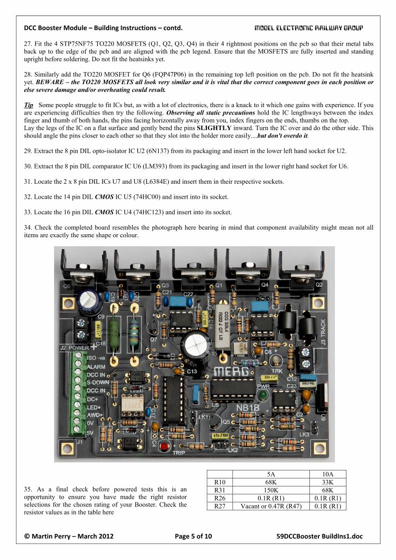
27. Fit the 4 STP75NF75 TO220 MOSFETS (Q1, Q2, Q3, Q4) in their 4 rightmost positions on the pcb so that their metal tabs back up to the edge of the pcb and are aligned with the pcb legend. Ensure that the MOSFETS are fully inserted and standing upright before soldering. Do not fit the heatsinks yet. 28. Similarly add the TO220 MOSFET for Q6 (FQP47P06) in the remaining top left position on the pcb. Do not fit the heatsink yet. BEWARE – the TO220 MOSFETS all look very similar and it is vital that the correct component goes in each position or else severe damage and/or overheating could result. Tip Some people struggle to fit ICs but, as with a lot of electronics, there is a knack to it which one gains with experience. If you are experiencing difficulties then try the following. Observing all static precautions hold the IC lengthways between the index finger and thumb of both hands, the pins facing horizontally away from you, index fingers on the ends, thumbs on the top. Lay the legs of the IC on a flat surface and gently bend the pins SLIGHTLY inward. Turn the IC over and do the other side. This should angle the pins closer to each other so that they slot into the holder more easily....but don't overdo it. 29. Extract the 8 pin DIL opto-isolator IC U2 (6N137) from its packaging and insert in the lower left hand socket for U2. 30. Extract the 8 pin DIL comparator IC U6 (LM393) from its packaging and insert in the lower right hand socket for U6. 31. Locate the 2 x 8 pin DIL ICs U7 and U8 (L6384E) and insert them in their respective sockets. 32. Locate the 14 pin DIL CMOS IC U5 (74HC00) and insert into its socket. 33. Locate the 16 pin DIL CMOS IC U4 (74HC123) and insert into its socket. 34. Check the completed board resembles the photograph here bearing in mind that component availability might mean not all items are exactly the same shape or colour.
35. As a final check before powered tests this is an opportunity to ensure you have made the right resistor selections for the chosen rating of your Booster. Check the resistor values as in the table here
5A 10A
R10 68K 33K R31 150K 68K R26 0.1R (R1) 0.1R (R1) R27 Vacant or 0.47R (R47) 0.1R (R1)
DCC Booster Module – Building Instructions – contd. MODEL ELECTRONIC RAILWAY GROUP
© Martin Perry – March 2012 Page 6 of 10 59DCCBooster BuildIns1.doc
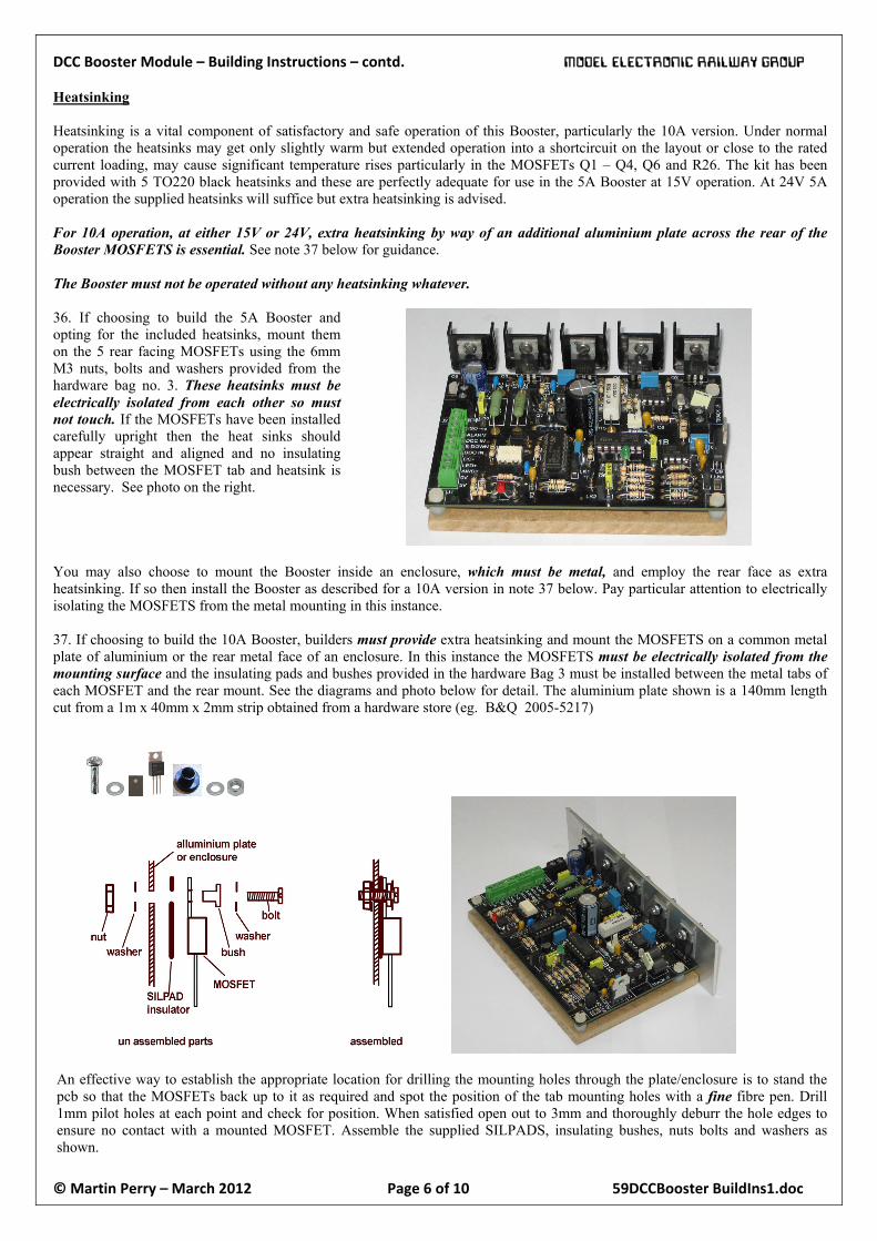
Heatsinking Heatsinking is a vital component of satisfactory and safe operation of this Booster, particularly the 10A version. Under normal operation the heatsinks may get only slightly warm but extended operation into a shortcircuit on the layout or close to the rated current loading, may cause significant temperature rises particularly in the MOSFETs Q1 – Q4, Q6 and R26. The kit has been provided with 5 TO220 black heatsinks and these are perfectly adequate for use in the 5A Booster at 15V operation. At 24V 5A operation the supplied heatsinks will suffice but extra heatsinking is advised. For 10A operation, at either 15V or 24V, extra heatsinking by way of an additional aluminium plate across the rear of the Booster MOSFETS is essential. See note 37 below for guidance. The Booster must not be operated without any heatsinking whatever. 36. If choosing to build the 5A Booster and opting for the included heatsinks, mount them on the 5 rear facing MOSFETs using the 6mm M3 nuts, bolts and washers provided from the hardware bag no. 3. These heatsinks must be electrically isolated from each other so must not touch. If the MOSFETs have been installed carefully upright then the heat sinks should appear straight and aligned and no insulating bush between the MOSFET tab and heatsink is necessary. See photo on the right.
You may also choose to mount the Booster inside an enclosure, which must be metal, and employ the rear face as extra heatsinking. If so then install the Booster as described for a 10A version in note 37 below. Pay particular attention to electrically isolating the MOSFETS from the metal mounting in this instance. 37. If choosing to build the 10A Booster, builders must provide extra heatsinking and mount the MOSFETS on a common metal plate of aluminium or the rear metal face of an enclosure. In this instance the MOSFETS must be electrically isolated from the mounting surface and the insulating pads and bushes provided in the hardware Bag 3 must be installed between the metal tabs of each MOSFET and the rear mount. See the diagrams and photo below for detail. The aluminium plate shown is a 140mm length cut from a 1m x 40mm x 2mm strip obtained from a hardware store (eg. B&Q 2005-5217)
An effective way to establish the appropriate location for drilling the mounting holes through the plate/enclosure is to stand the pcb so that the MOSFETs back up to it as required and spot the position of the tab mounting holes with a fine fibre pen. Drill 1mm pilot holes at each point and check for position. When satisfied open out to 3mm and thoroughly deburr the hole edges to ensure no contact with a mounted MOSFET. Assemble the supplied SILPADS, insulating bushes, nuts bolts and washers as shown.

DCC Booster Module – Building Instructions – contd. MODEL ELECTRONIC RAILWAY GROUP
© Martin Perry – March 2012 Page 7 of 10 59DCCBooster BuildIns1.doc
When completed, use a standard multimeter on its resistance range to check for electrical connection between each MOSFET tab and the mounting plate/enclosure. If correctly mounted there should be no direct electrical connection at 0 ohms. A DVM will indicate infinite resistance and an AVM will display no deflection of the meter needle. However, be aware that if the pcb is mounted onto an angled plate or enclosure using metal spacers or stand-offs then the pcb ground plane and the plate/enclosure will be electrically connected and a small degree of conductivity may be apparent through the MOSFETS themselves. If in any doubt seek advice from MERG Technical Support. The Booster design also incorporates a facility for attaching a thermal cutout (eg. Type Fc-p2d 60degC Rapid Electronics ref 61-2076 – not supplied in the kit) which should be firmly attached to the Q6 heatsink if very high currents are to be expected. The electrical leads of the cutout are connected in place of the normally present link LK1 which should be removed. The cutout removes DCC drive from the output H-bridge if its operating temperature is exceeded and may take several minutes to cool enough to re-establish Booster operation. Having completed the provisions for heatsinking in either section 36. or 37. above then your Booster is ready for final electrical testing. Final Electrical Testing
38. To test your Booster you will need the following: a. A source of DCC input signal from a system Command Station such as the SPROG or the MERG CAN-CMD module (Kit 91) connected to Booster J1 pins 3 and 5. Polarity can be important in ensuring the Booster powers up correctly. If this signal is absent the Booster reverts to shutdown mode which is a normal protective function and avoids damaging static DC voltage appearing across the track. Connect from the CAN-CMD module J5 pins 3 and 1 to the Booster J1 pins 5 and 3 respectively. On the CAN-CMD module jumper J7 must be absent and on the NB1B Booster link LK1 must be present. b. A connection from your chosen voltage (13.8V – 25VDC) Regulated Power Supply (eg. the MERG 15Vdc 6A SMPS Kit 774) to J2. The +ve terminal is clearly marked and it is vital that connection polarity is carefully observed. The NB1B Booster does not have any protection against reversed connection since inclusion of the necessary components would involve unproductive heating and power loss in normal operation. The output voltage of your chosen power supply determines the Booster’s applied track voltage which may be up to a volt less than the applied input voltage, depending on current drawn, and for the vast majority of circumstances 15V is adequate for scales up to modern 0-gauge locomotives. c. The supplied Audible Warning Device (AWD) is connected to J1/8 (+ve) and J1/9 (-ve). 39. Apply the DCC input signal first followed by the DC Power Source. The green PWR LED should illuminate and the track output TRK LED should show orange. If it shows either red or green then there is a fault and your assembly must be depowered and checked again for short circuits. At this point, the red TRIP LED should be dark. Wait 30 seconds and then repeat the preliminary electrical tests specified in paragraphs 25. and 26. above remembering that, now the IC sockets are populated, it is vital not to short adjacent IC pins with your meter probes. 40. Remove the DCC input signal from J1 and the Booster should enter shutdown mode. The TRK LED should go dark and red TRIP LED illuminate. The AWD will emit a continuous tone. Reapply DCC and the Booster reverts to normal operation. 41. To test short circuit protection apply a short circuit across the track output terminal block J3. The Booster should enter shutdown mode and commence retrying every 2 seconds. This will be evident from the AWD and TRK/TRIP LEDs alternating. 42. To test remote shutdown connect J1 pins 4 and 6 with a short loop of wire and then apply another between J1 pins 1 and 9. This simulates a remote panel switch requesting the Booster to shutdown under control from a layout operator. The TRIP LED and AWD should behave as in paragraph 40 above. This function will also be available from CAN-CAB handsets via the CAN-CMD module in the future. Your Booster is now ready to be connected to the track for running trains. Please pay particular attention to the notes on operation, cabling and correct connection on the following page. Acknowledgements Original NB1B design - Mike Bolton M786 Production Engineering - Trevor Stockill M2433 and Martin Perry M1481 PCB layout - Trevor Stockill M2433 Kit Crafting and Documentation – Martin Perry M1481
DCC Booster Module – Building Instructions – contd. MODEL ELECTRONIC RAILWAY GROUP
© Martin Perry – March 2012 Page 8 of 10 59DCCBooster BuildIns1.doc
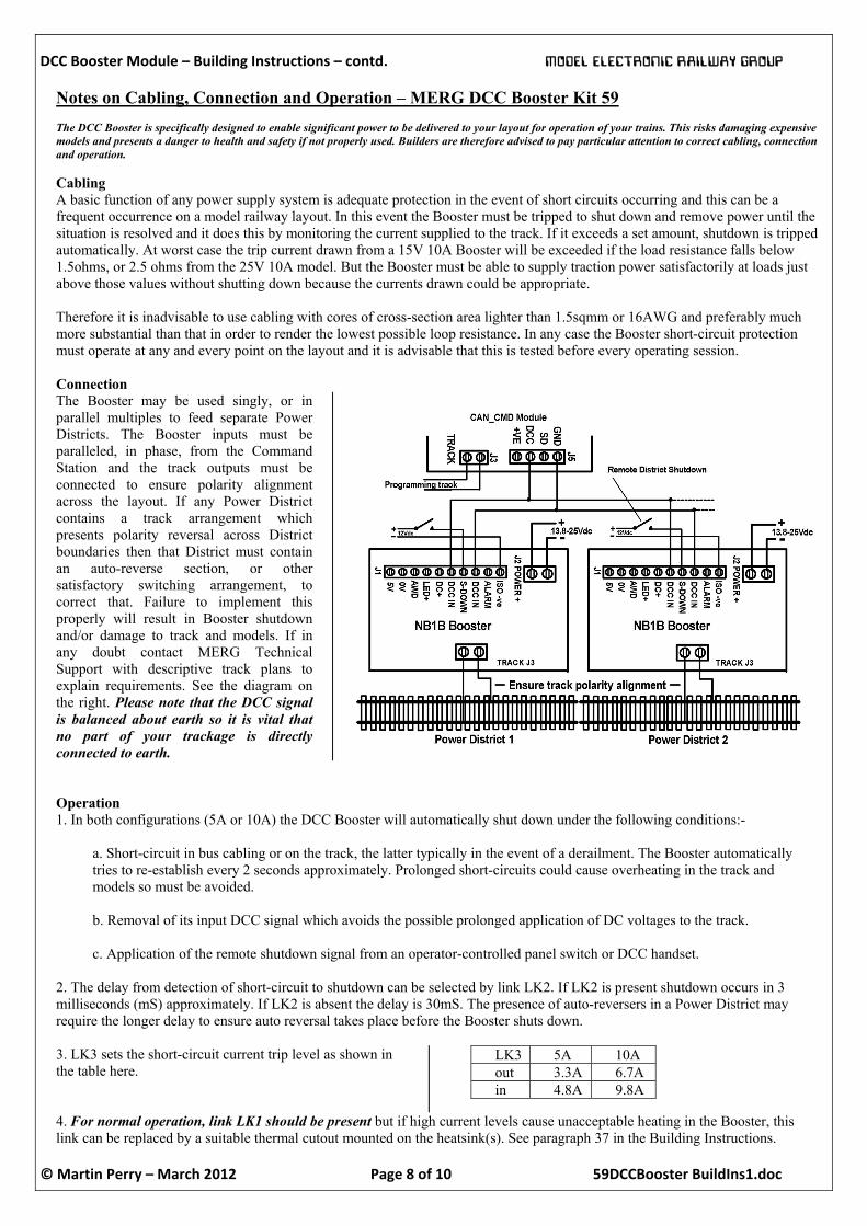
Notes on Cabling, Connection and Operation – MERG DCC Booster Kit 59 The DCC Booster is specifically designed to enable significant power to be delivered to your layout for operation of your trains. This risks damaging expensive models and presents a danger to health and safety if not properly used. Builders are therefore advised to pay particular attention to correct cabling, connection and operation. Cabling A basic function of any power supply system is adequate protection in the event of short circuits occurring and this can be a frequent occurrence on a model railway layout. In this event the Booster must be tripped to shut down and remove power until the situation is resolved and it does this by monitoring the current supplied to the track. If it exceeds a set amount, shutdown is tripped automatically. At worst case the trip current drawn from a 15V 10A Booster will be exceeded if the load resistance falls below 1.5ohms, or 2.5 ohms from the 25V 10A model. But the Booster must be able to supply traction power satisfactorily at loads just above those values without shutting down because the currents drawn could be appropriate. Therefore it is inadvisable to use cabling with cores of cross-section area lighter than 1.5sqmm or 16AWG and preferably much more substantial than that in order to render the lowest possible loop resistance. In any case the Booster short-circuit protection must operate at any and every point on the layout and it is advisable that this is tested before every operating session. Connection The Booster may be used singly, or in parallel multiples to feed separate Power Districts. The Booster inputs must be paralleled, in phase, from the Command Station and the track outputs must be connected to ensure polarity alignment across the layout. If any Power District contains a track arrangement which presents polarity reversal across District boundaries then that District must contain an auto-reverse section, or other satisfactory switching arrangement, to correct that. Failure to implement this properly will result in Booster shutdown and/or damage to track and models. If in any doubt contact MERG Technical Support with descriptive track plans to explain requirements. See the diagram on the right. Please note that the DCC signal is balanced about earth so it is vital that no part of your trackage is directly connected to earth.
Operation 1. In both configurations (5A or 10A) the DCC Booster will automatically shut down under the following conditions:-
a. Short-circuit in bus cabling or on the track, the latter typically in the event of a derailment. The Booster automatically tries to re-establish every 2 seconds approximately. Prolonged short-circuits could cause overheating in the track and models so must be avoided.
b. Removal of its input DCC signal which avoids the possible prolonged application of DC voltages to the track.
c. Application of the remote shutdown signal from an operator-controlled panel switch or DCC handset.
2. The delay from detection of short-circuit to shutdown can be selected by link LK2. If LK2 is present shutdown occurs in 3 milliseconds (mS) approximately. If LK2 is absent the delay is 30mS. The presence of auto-reversers in a Power District may require the longer delay to ensure auto reversal takes place before the Booster shuts down. 3. LK3 sets the short-circuit current trip level as shown in the table here.
LK3 5A 10A out 3.3A 6.7A in 4.8A 9.8A
4. For normal operation, link LK1 should be present but if high current levels cause unacceptable heating in the Booster, this link can be replaced by a suitable thermal cutout mounted on the heatsink(s). See paragraph 37 in the Building Instructions.
DCC Booster Module – Building Instructions – contd. MODEL ELECTRONIC RAILWAY GROUP
© Martin Perry – March 2012 Page 9 of 10 59DCCBooster BuildIns1.doc
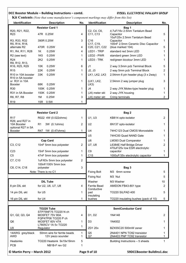
Kit Contents (Note that some manufacturer’s component markings may differ from this list) Identification Description No. Identification Description No.
Resistor Card 1 Bag 1 R20, R21, R22, R23 47R 0.25W 4
C2, C4, C6, C11, C13
4.7uF/16v 2.5mm Tantalum Bead Capacitor
5
R3, R33, R32 390R 0.25W 3 C16 10uF/25v 2.5mm Tantalum Bead Capacitor 1
R5, R14, R18, alternate R2 470R 0.25W 4
C17, C19, C20, C21, C22
100nF 2.5mm Ceramic Disc Capacitor (blue marked 104) 5
R1, R4, R11, R28 1K 0.25W 4 LED1 - TRIP standard red 3mm LED 1 R2 (see text) 1K5 0.25W 1 LED2 - PWR standard green 3mm LED 1 R24 2K2 0.25W 1 LED3 - TRK red/green bicolour 3mm LED 1 R9, R12, R13, R16, R25, R29 10K 0.25W 6 J1 2 way 3.5mm pcb Terminal Block 5 R15 22K 0.25W 1 J2, J3 2 way 5mm pcb Terminal Block 2 R10 in 10A booster 33K 0.25W 1 LK1, LK2, LK3 2.54mm 6 pin header plug (3 x 2way) 1 R10 in 5A booster or R31 in 10A Booster 68K 0.25W
1
(LK1, LK2, LK3)
2.54mm 2 way jumper plug 3
R30 100K 0.25W 1 J4 2 way JYK Molex-type header plug 1 R31 in 5A Booster 150K 0.25W 1 (J4) meter skt 2 way JYK housing 1 R6, R7, R8 1M 0.25W 3 (J4) meter skt Crimp terminals 2
R19 15R 0.5W 1
Resistor Card 2 Bag 2
R17 R022 4W (0.022ohms) 1 U1, U3 KB814 opto-isolator 2 R26; and R27 in 10A Booster R1 3W (0.1ohms) 2 U2 6N137 opto-isolator 1 optional R27 in 5A Booster R47 1W (0.47ohms) 1 U4 74HC123 Dual CMOS Monostable 1
U5 74HC00 Quad NAND Gate 1
Cap Card U6 LM393 Dual Comparator 1 C3, C12 10nF 5mm box polyester 2 U7, U8 L6384E Half Bridge Driver 2
C23 15nF 5mm box polyester 1 C9 470uF/25v low ESR electrolytic capacitor 1
C5 47nF 5mm box polyester 1 C15 1000uF/35v electrolytic capacitor 1
C7, C10 1uF/63v 5mm box polyester 2
C8, C14, C18 100nF/100V 5mm box polyester 3 Bag 3
Note: There is no C1 Fixing Bolt M3 6mm screw 5
Fixing Nut M3 Nut 5
DIL Tube Washer M3 Washer 10 8 pin DIL skt for U2, U6, U7, U8 4 Ferrite Bead AMIDON FB43-801 type 2
14 pin DIL skt for U5 1 Conductive pad TO220 SILPAD 400 5
16 pin DIL skt for U4 1 insulating bushes TO220 insulating bushes (pack of 10) 5
TO220 Tube SemiConductor Card
Q1, Q2, Q3, Q4 STP75NF75 TO220 N ch MOSFET 75V 80A 4 D1, D2 1N4148 2
Q6 FQP47P06 TO220 P ch MOSFET 60V 47A 1 D3 1N4002 1
U9 L7805CV 1A 5v TO220 Regulator 1 ZD1 20v BZX55C20 500mW zener 1
14AWG grey/black 50mm wire for ferrite beads 1 Q5 2N4401 NPN TO92 transistor 1 AWD 12V piezo sounder 1 Q7 2N4403 PNP TO92 transistor 1
Heatsinks TO220 Heatsink 9x19x19mm 5 Building Instructions – 5 sheets 1 PCB NB1B-F rev G2 1
DCC Booster Module – Building Instructions – contd. MODEL ELECTRONIC RAILWAY GROUP
© Martin Perry – March 2012 Page 10 of 10 59DCCBooster BuildIns1.doc