december 2011 samsung - arm开发板|嵌入式开发 … of figures figure title page number number...
TRANSCRIPT
S5M8767A
Power Management IC for Mobile Applications
Revision 0.10
December 2011
DDaattaa SShheeeett
2011 Samsung Electronics Co., Ltd. All rights reserved.
si-plaza / Jeff_cui at 14:14,2011.12.13
SAMSUNG
Important Notice
Samsung Electronics Co. Ltd. (“Samsung”) reserves the
right to make changes to the information in this publication
at any time without prior notice. All information provided is
for reference purpose only. Samsung assumes no
responsibility for possible errors or omissions, or for any
consequences resulting from the use of the information
contained herein.
This publication on its own does not convey any license,
either express or implied, relating to any Samsung and/or
third-party products, under the intellectual property rights of
Samsung and/or any third parties.
Samsung makes no warranty, representation, or guarantee
regarding the suitability of its products for any particular
purpose, nor does Samsung assume any liability arising out
of the application or use of any product or circuit and
specifically disclaims any and all liability, including without
limitation any consequential or incidental damages.
Customers are responsible for their own products and
applications. "Typical" parameters can and do vary in
different applications. All operating parameters, including
"Typicals" must be validated for each customer application
by the customer's technical experts.
Samsung products are not designed, intended, or authorized
for use in applications intended to support or sustain life, or
for any other application in which the failure of the Samsung
product could reasonably be expected to create a situation
where personal injury or death may occur. Customers
acknowledge and agree that they are solely responsible to
meet all other legal and regulatory requirements regarding
their applications using Samsung products notwithstanding
any information provided in this publication. Customer shall
indemnify and hold Samsung and its officers, employees,
subsidiaries, affiliates, and distributors harmless against all
claims, costs, damages, expenses, and reasonable attorney
fees arising out of, either directly or indirectly, any claim
(including but not limited to personal injury or death) that
may be associated with such unintended, unauthorized
and/or illegal use.
WARNING No part of this publication may be reproduced,
stored in a retrieval system, or transmitted in any form or by
any means, electric or mechanical, by photocopying,
recording, or otherwise, without the prior written consent of
Samsung. This publication is intended for use by designated
recipients only. This publication contains confidential
information (including trade secrets) of Samsung protected
by Competition Law, Trade Secrets Protection Act and other
related laws, and therefore may not be, in part or in whole,
directly or indirectly publicized, distributed, photocopied or
used (including in a posting on the Internet where
unspecified access is possible) by any unauthorized third
party. Samsung reserves its right to take any and all
measures both in equity and law available to it and claim full
damages against any party that misappropriates Samsung’s
trade secrets and/or confidential information.
警 告 本文件仅向经韩国三星电子株式会社授权的人员提供,
其内容含有商业秘密保护相关法规规定并受其保护的三星电
子株式会社商业秘密,任何直接或间接非法向第三人披露、
传播、复制或允许第三人使用该文件全部或部分内容的行为
(包括在互联网等公开媒介刊登该商业秘密而可能导致不特
定第三人获取相关信息的行为)皆为法律严格禁止。此等违
法行为一经发现,三星电子株式会社有权根据相关法规对其
采取法律措施,包括但不限于提出损害赔偿请求。
Copyright 2011 Samsung Electronics Co., Ltd.
Samsung Electronics Co., Ltd.
San #24 Nongseo-Dong, Giheung-Gu
Yongin-City, Gyeonggi-Do, Korea 446-711
Contact Us: [email protected]
TEL: (82)-(31)-209-9287
FAX: (82)-(31)-209-3131
Home Page: http://www.samsungsemi.com
si-plaza / Jeff_cui at 14:14,2011.12.13
SAMSUNG

Trademarks
All brand names, trademarks and registered trademarks belong to their respective owners.
Exynos, Exynos4210, FlexOneNAND, and OneNAND are trademarks of Samsung Electronics.
ARM, Jazelle, TrustZone, and Thumb are registered trademarks of ARM Limited. Cortex, ETM, ETB,
Coresight, ISA, and Neon are trademarks of ARM Limited.
Java is a trademark of Sun Microsystems, Inc.
SD is a registered trademark of Toshiba Corporation.
MMC and eMMC are trademarks of MultiMediaCard Association.
JTAG is a registered trademark of JTAG Technologies, Inc.
Synopsys is a registered trademark of Synopsys, Inc.
I2S is a trademark of Phillips Electronics.
I2C is a trademark of Phillips Semiconductor Corp.
MIPI and Slimbus are registered trademarks of the Mobile Industry Processor Interface (MIPI) Alliance.
All other trademarks used in this publication are the property of their respective owners.
si-plaza / Jeff_cui at 14:14,2011.12.13
SAMSUNG
Chip Handling Guide
Precaution against Electrostatic Discharge
When handling semiconductor devices, be sure that the environment is protected against static electricity.
1. Operators should wear anti-static clothing and use earth band.
2. All objects that come in direct contact with devices should be made of materials that do not produce static
electricity that would cause damage.
3. Equipment and work table must be earthed.
4. Ionizer is recommended to remove electron charge.
Contamination
Be sure to use semiconductor products in the environment that may not be exposed to dust or dirt adhesion.
Temperature/Humidity
Semiconductor devices are sensitive to environment temperature and humidity. High temperature or humidity may
deteriorate semiconductor device’s characteristics. Therefore avoid storage or use in such conditions.
Mechanical Shock
Care should be exercised not to apply excessive mechanical shock or force on semiconductor device.
Chemical
Do not expose semiconductor device to chemical because reaction to chemical may cause deterioration of device
characteristics.
Light Protection
In case of non-EMC (Epoxy Molding Compound) package, do not expose semiconductor IC to strong light. It may
cause device’s malfunction. (But, some special products which utilize the light or have security function are
excepted from this guide)
Radioactive, Cosmic and X-ray
Semiconductor devices can be influenced by radioactive, cosmic ray or X-ray. Radioactive, cosmic and X-ray may
cause soft error during device operation. Therefore semiconductor devices must be shielded under environment
that may be exposed to radioactive, cosmic ray or X-ray.
EMS (Electromagnetic Susceptibility)
Note that semiconductor device’s characteristics may be affected by strong electromagnetic wave or magnetic
field during operation under insufficient PCB circuit design for EMS.
si-plaza / Jeff_cui at 14:14,2011.12.13
SAMSUNG
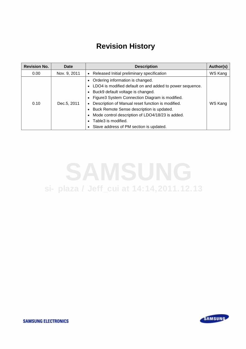
Revision History
Revision No. Date Description Author(s)
0.00 Nov. 9, 2011 Released Initial preliminary specification WS Kang
0.10 Dec.5, 2011
Ordering information is changed.
LDO4 is modified default on and added to power sequence.
Buck9 default voltage is changed.
Figure3 System Connection Diagram is modified.
Description of Manual reset function is modified.
Buck Remote Sense description is updated.
Mode control description of LDO4/18/23 is added.
Table3 is modified.
Slave address of PM section is updated.
WS Kang
si-plaza / Jeff_cui at 14:14,2011.12.13
SAMSUNG

Table of Contents
1 PRODUCT OVERVIEW .................................................................................. 11
1.1 Introduction ................................................................................................................................................ 11 1.2 Features ..................................................................................................................................................... 12
1.2.1 Regulators .......................................................................................................................................... 12 1.2.2 Supplementary Functions ................................................................................................................... 13 1.2.3 Applications ........................................................................................................................................ 13 1.2.4 Ordering Information ........................................................................................................................... 13
1.3 Block Diagram ............................................................................................................................................ 14 1.4 Ball Configuration (Top View) .................................................................................................................... 16 1.5 Ball Description .......................................................................................................................................... 17 1.6 Absolute Maximum Ratings ....................................................................................................................... 22 1.7 Recommended Operating Condition ......................................................................................................... 22
2 ELECTRICAL SPECIFICATIONS ................................................................... 23
2.1 General and Logic ...................................................................................................................................... 23 2.2 Buck Converters......................................................................................................................................... 25
2.2.1 Buck Converter 1, 3, 5, 6, 7, 8, 9 ........................................................................................................ 25 2.2.2 Buck Converter 2 & 4 ......................................................................................................................... 27
2.3 LDOs .......................................................................................................................................................... 29 2.3.1 LDO (P) 4, 5, 11, 12, 13, 14, 16, 17, 19, 20, 21, 22, 26, 27, 28 (150 mA, PMOS) ............................ 29 2.3.2 LDO (P) 3, 10, 18, 23, 24, 25 (300 mA, PMOS) ................................................................................. 32 2.3.3 LDO (P) 9 (400 mA, PMOS) ............................................................................................................... 35 2.3.4 LDO (N) 1, 6, 7, 15 (150 mA, NMOS)................................................................................................. 38 2.3.5 LDO (N) 8 (300 mA, NMOS) ............................................................................................................... 41 2.3.6 LDO (N) 2 (450 mA, NMOS) ............................................................................................................... 44
2.4 Backup Coin Battery Charger .................................................................................................................... 46 2.5 Clock and RTC ........................................................................................................................................... 48
3 FUNCTIONAL DESCRIPTION ........................................................................ 49
3.1 Power Sequence ........................................................................................................................................ 49 3.1.1 Power On Sequence .......................................................................................................................... 49 3.1.2 MR, SMPL, WTSR, RTC, POR, IRQB................................................................................................ 54
3.2 UVLO, Reference Voltage, Thermal Shutdown ......................................................................................... 58 3.3 Regulator .................................................................................................................................................... 59
3.3.1 Buck Converters ................................................................................................................................. 59 3.3.2 LDOs ................................................................................................................................................... 64
3.4 Backup Coin Battery .................................................................................................................................. 69 3.4.1 Backup Coin Battery ........................................................................................................................... 69
4 DIGITAL INTERFACE (I2C) ........................................................................... 70
4.1 Slave Address ............................................................................................................................................ 70 4.2 Register Address........................................................................................................................................ 71
4.2.1 I2C Interface ....................................................................................................................................... 71 4.2.2 Control Interface using SCL (Clock) and SDA (Data) ........................................................................ 71 4.2.3 I2C Interface Timing Diagram ............................................................................................................. 73
si-plaza / Jeff_cui at 14:14,2011.12.13
SAMSUNG
5 REGISTER DESCRIPTION ............................................................................ 75
5.1 Power Management ................................................................................................................................... 75 5.1.1 Register Map Summary ...................................................................................................................... 75 5.1.2 Bit Map Summary ............................................................................................................................... 79
5.2 RTC .......................................................................................................................................................... 113 5.2.1 Register Map Summary .................................................................................................................... 113 5.2.2 Bit Map Summary ............................................................................................................................. 114
6 APPLICATION CIRCUIT .............................................................................. 127
6.1 Package Dimension ................................................................................................................................. 128
si-plaza / Jeff_cui at 14:14,2011.12.13
SAMSUNG
List of Figures
Figure Title Page
Number Number
Figure 1 S5M8767A Package Top and Bottom Views ......................................................................................... 11 Figure 2 Block Diagram of S5M8767A ................................................................................................................. 14 Figure 3 System Connection Diagram ................................................................................................................. 15 Figure 4 Ball Configuration ................................................................................................................................... 16 Figure 5 Power On Sequence .............................................................................................................................. 51 Figure 6 Power on/off Sequence .......................................................................................................................... 52 Figure 7 Sleep and Wakeup by PWREN ............................................................................................................. 53 Figure 8 Manual Reset Sequence Timing Diagram ............................................................................................. 54 Figure 9 SMPL Timing Diagram ........................................................................................................................... 55 Figure 10 WTSR Timing Diagram ........................................................................................................................ 56 Figure 11 Power On Debounce and Interrupt ...................................................................................................... 57 Figure 12 Buck Converter Block Diagram ............................................................................................................ 59 Figure 13 Power On Sequence in Buck Converter .............................................................................................. 59 Figure 14 Buck2/3/4 DVS Control ........................................................................................................................ 60 Figure 15 Remote Sense Pin Connection ............................................................................................................ 60 Figure 16 SW Node Voltage and Inductor Current Waveforms in Dual Phase Buck Converter ......................... 61 Figure 17 Mode Transition Waveforms in Buck 5 ................................................................................................ 61 Figure 18 PLDO (Low-Dropout Regulator having a PMOS Power Transistor) .................................................... 64 Figure 19 Application Example ............................................................................................................................ 65 Figure 20 NLDO (Low-Dropout Regulator having a NMOS Power Transistor) ................................................... 66 Figure 21 Mode Control Waveforms in LDO4,LDO18 and LDO 23 ..................................................................... 67 Figure 22 Backup Coin Battery Charging Graph ................................................................................................. 69 Figure 23 Single Byte Write Mode ....................................................................................................................... 71 Figure 24 Multi Bytes Write Mode ........................................................................................................................ 71 Figure 25 Single Byte Read Mode ....................................................................................................................... 72 Figure 26 Multi Bytes Read Mode ........................................................................................................................ 72 Figure 27 I2C Control Interface Timing Diagram ................................................................................................. 73 Figure 28 Typical Application Circuit .................................................................................................................. 127 Figure 29 Package Dimension ........................................................................................................................... 128
si-plaza / Jeff_cui at 14:14,2011.12.13
SAMSUNG
List of Tables
Table Title Page
Number Number
Table 1 List of Recommended Inductors ............................................................................................................. 62 Table 2 List of Recommended Capacitors ........................................................................................................... 63 Table 3 Information of Power Supply on Each LDO ............................................................................................ 68 Table 4 I2C Electrical Specification ...................................................................................................................... 74 Table 5 Voltage Table for BUCK 2/3/4 ............................................................................................................... 104 Table 6 Voltage Table for BUCK1/5/6 ................................................................................................................ 105 Table 7 Voltage Table for BUCK7/8/9 ................................................................................................................ 106
si-plaza / Jeff_cui at 14:14,2011.12.13
SAMSUNG

List of Conventions
Register RW Access Type Conventions
Type Definition Description
R Read Only The application has permission to read the Register field. Writes to read-only fields
have no effect.
W Write Only The application has permission to write in the Register field.
RW Read & Write The application has permission to read and writes in the Register field. The
application sets this field by writing 1’b1 and clears it by writing 1’b0.
RC Read & Clear If reading 0x01 to 0x03 registers, the information is automatically cleared.
Register Value Conventions
Expression Description
x Undefined bit
X Undefined multiple bits
? Undefined, but depends on the device or pin status
Device dependent The value depends on the device
Pin value The value depends on the pin status
Reset Value Conventions
Expression Description
0
1
x
Warning: Some bits of control registers are driven by hardware or write only. As a result the indicated reset
value and the read value after reset might be different.
si-plaza / Jeff_cui at 14:14,2011.12.13
SAMSUNG

Samsung Confidential S5M8767A_Data Sheet_REV0.10 (Preliminary Spec) 1 Product Overview
11
Preliminary product information describes products that are in development, for which full characterization data and
associated errata are not yet available. Specifications and information herein are subject to change without notice.
1 Product Overview
1.1 Introduction
S5M8767A is an advanced Power Management IC (PMIC) designed for mobile applications. It is comprised of
high efficient Buck converters including Dual-Phase Buck converters, various LDOs, and an RTC integrated into a
144-WFP (Wafer-level Fabricated Package), 5.0mm 5.0mm package.
S5M8767A, coupled with Multi Core Samsung Application Processors (Exynos4212/4412/5250), is used in wide
mobile applications such as smart phones and tablet PCs.
The Buck Converters in S5M8767A provide stable power to the ARM core/cache, internal logic, memory, camera
processor, and sub-regulations. Three Buck Converters for high load capacity in Application Processor side also
provide optimal power control using Dynamic Voltage Scaling (DVS) via I2C or GPIO interface between PMIC and
Application Processor.
The various LDOs supply appropriate power to each I/O and functional block in an Application Processor and
camera IC in set application. Applying independent LDO to each I/O block helps the CPU to support various types
of devices. Each block can be turned on and turned off for power optimization. Other features include thermal
regulation and internal timer function.
144 WFP-5.0mm 5.0mm, 0.4mm pitch
Top View Bottom View
Figure 1 S5M8767A Package Top and Bottom Views
si-plaza / Jeff_cui at 14:14,2011.12.13
SAMSUNG
Samsung Confidential S5M8767A_Data Sheet_REV0.10 (Preliminary Spec) 1 Product Overview
12
Preliminary product information describes products that are in development, for which full characterization data and
associated errata are not yet available. Specifications and information herein are subject to change without notice.
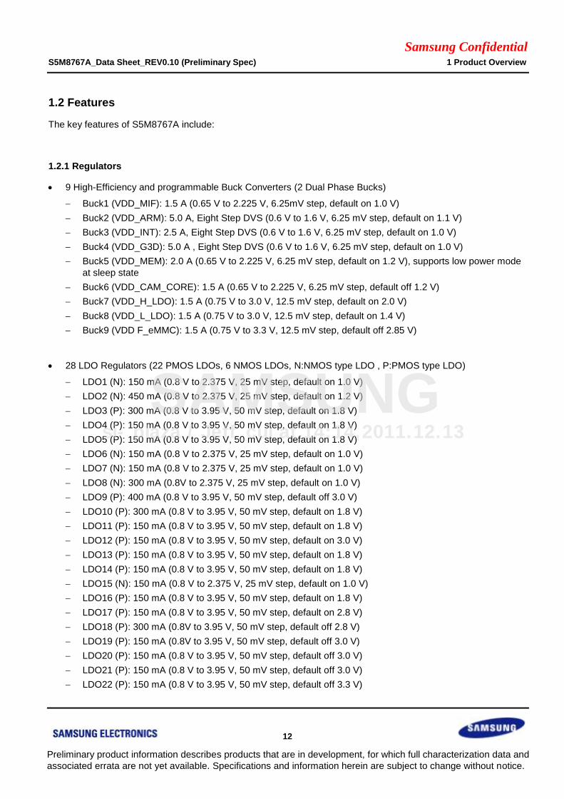
1.2 Features
The key features of S5M8767A include:
1.2.1 Regulators
9 High-Efficiency and programmable Buck Converters (2 Dual Phase Bucks)
Buck1 (VDD_MIF): 1.5 A (0.65 V to 2.225 V, 6.25mV step, default on 1.0 V)
Buck2 (VDD_ARM): 5.0 A, Eight Step DVS (0.6 V to 1.6 V, 6.25 mV step, default on 1.1 V)
Buck3 (VDD_INT): 2.5 A, Eight Step DVS (0.6 V to 1.6 V, 6.25 mV step, default on 1.0 V)
Buck4 (VDD_G3D): 5.0 A , Eight Step DVS (0.6 V to 1.6 V, 6.25 mV step, default on 1.0 V)
Buck5 (VDD_MEM): 2.0 A (0.65 V to 2.225 V, 6.25 mV step, default on 1.2 V), supports low power mode
at sleep state
Buck6 (VDD_CAM_CORE): 1.5 A (0.65 V to 2.225 V, 6.25 mV step, default off 1.2 V)
Buck7 (VDD_H_LDO): 1.5 A (0.75 V to 3.0 V, 12.5 mV step, default on 2.0 V)
Buck8 (VDD_L_LDO): 1.5 A (0.75 V to 3.0 V, 12.5 mV step, default on 1.4 V)
Buck9 (VDD F_eMMC): 1.5 A (0.75 V to 3.3 V, 12.5 mV step, default off 2.85 V)
28 LDO Regulators (22 PMOS LDOs, 6 NMOS LDOs, N:NMOS type LDO , P:PMOS type LDO)
LDO1 (N): 150 mA (0.8 V to 2.375 V, 25 mV step, default on 1.0 V)
LDO2 (N): 450 mA (0.8 V to 2.375 V, 25 mV step, default on 1.2 V)
LDO3 (P): 300 mA (0.8 V to 3.95 V, 50 mV step, default on 1.8 V)
LDO4 (P): 150 mA (0.8 V to 3.95 V, 50 mV step, default on 1.8 V)
LDO5 (P): 150 mA (0.8 V to 3.95 V, 50 mV step, default on 1.8 V)
LDO6 (N): 150 mA (0.8 V to 2.375 V, 25 mV step, default on 1.0 V)
LDO7 (N): 150 mA (0.8 V to 2.375 V, 25 mV step, default on 1.0 V)
LDO8 (N): 300 mA (0.8V to 2.375 V, 25 mV step, default on 1.0 V)
LDO9 (P): 400 mA (0.8 V to 3.95 V, 50 mV step, default off 3.0 V)
LDO10 (P): 300 mA (0.8 V to 3.95 V, 50 mV step, default on 1.8 V)
LDO11 (P): 150 mA (0.8 V to 3.95 V, 50 mV step, default on 1.8 V)
LDO12 (P): 150 mA (0.8 V to 3.95 V, 50 mV step, default on 3.0 V)
LDO13 (P): 150 mA (0.8 V to 3.95 V, 50 mV step, default on 1.8 V)
LDO14 (P): 150 mA (0.8 V to 3.95 V, 50 mV step, default on 1.8 V)
LDO15 (N): 150 mA (0.8 V to 2.375 V, 25 mV step, default on 1.0 V)
LDO16 (P): 150 mA (0.8 V to 3.95 V, 50 mV step, default on 1.8 V)
LDO17 (P): 150 mA (0.8 V to 3.95 V, 50 mV step, default on 2.8 V)
LDO18 (P): 300 mA (0.8V to 3.95 V, 50 mV step, default off 2.8 V)
LDO19 (P): 150 mA (0.8V to 3.95 V, 50 mV step, default off 3.0 V)
LDO20 (P): 150 mA (0.8 V to 3.95 V, 50 mV step, default off 3.0 V)
LDO21 (P): 150 mA (0.8 V to 3.95 V, 50 mV step, default off 3.0 V)
LDO22 (P): 150 mA (0.8 V to 3.95 V, 50 mV step, default off 3.3 V)
si-plaza / Jeff_cui at 14:14,2011.12.13
SAMSUNG
Samsung Confidential S5M8767A_Data Sheet_REV0.10 (Preliminary Spec) 1 Product Overview
13
Preliminary product information describes products that are in development, for which full characterization data and
associated errata are not yet available. Specifications and information herein are subject to change without notice.
LDO23 (P): 300 mA (0.8 V to 3.95 V, 50 mV step, default off 2.8 V)
LDO24 (P): 300 mA (0.8 V to 3.95 V, 50 mV step, default off 3.0 V)
LDO25 (P): 300 mA (0.8 V to 3.95 V, 50 mV step, default off 1.2 V)
LDO26 (P): 150 mA (0.8 V to 3.95 V, 50 mV step, default off 1.8 V)
LDO27 (P): 150 mA (0.8 V to 3.95 V, 50mV step, default off 1.8 V)
LDO28 (P): 150 mA (0.8 V to 3.95 V, 50 mV step, default off 1.8 V)
1.2.2 Supplementary Functions
RTC with two alarms
Three Buffered 32.768 kHz Outputs (for AP, CP, and B/T)
One Back up battery charger
Low-Battery Monitor and Reset Output
Under Voltage Lock Out / Thermal Shutdown / BandGap Reference
Power-on Sequence
I2C Interface for Programming
1.2.3 Applications
Smart Phones and Cellular Phones
Portable Applications (Tablet PC and Wireless Handheld)
1.2.4 Ordering Information
Device Package Operating Temperature
S5M8767A01-6030 (NOTE) 144 WFP – 5.0mm 5.0mm (0.4mm pitch) – 40C to 85C
NOTE: Under Development
Warning: This device should be shorted together or the device should be placed in conductive foam during
storage or handling to prevent electrostatic damage.
si-plaza / Jeff_cui at 14:14,2011.12.13
SAMSUNG

Samsung Confidential S5M8767A_Data Sheet_REV0.10 (Preliminary Spec) 1 Product Overview
14
Preliminary product information describes products that are in development, for which full characterization data and
associated errata are not yet available. Specifications and information herein are subject to change without notice.
1.3 Block Diagram
NC1
NC2
NC3
NC4
AG
ND
1
AG
ND
2
FB2
BS1
BS2
1.0
uH
10uF
VD
D_ARM
1.1
V /
5.0
A
VD
D_B2
BS3
10uF
PG
ND
2I2
C10uF
1.0
uH
32kHZ OSC
RTC
Backup Charger
Ba
cku
p
Ba
tte
ry
Ch
arg
er
0.2
2u
F
I2C
I2C
Divider
VBATT
AP32K
VD
D_CP32K
CP32K
BKCO
IN
XTALIN
XTALO
UT
FB1
EN_B1
1.0uH
10uF
VDD_DRAMC1.0V / 1.5A
VDD_B1
4.7uF
PGND1
LDO11150mA
EN
1u
F
IN3
IN9
EN
1u
F4.7
uF
2.2uF
IN1
2.2uF
IN1 1.0uF
IN2
1.0uF
IN3
1.0uF
IN1
2.2uF
IN2
1.0uF
IN1
1.0uF
IN2
2.2uF
IN4
1.0uF
IN5
1.0uF
IN4
2.2uF
IN6
1.0uF
IN5
1.0uF
IN7
2.2uF
IN5
1.0uF
IN5
1.0uF
IN6
2.2uF
IN6
1.0uF
IN6
1.0uF
IN7
1uF
IN8
1.0uF
IN8
1.0uF
IN8
1.0
uF
IN8
IN8
1.0
uF
TOP LOGIC
On/OffPower Sequence
&I2C
Interface
PWRON
JIGONB
PWRHOLD
ONOB
Reset I2C
TOP
RSOB
MR1B
MR2B
SCL
SDA
S5M8767A
BUCK61.5A
FB6
EN_B6
1.0uH
10uF
CAM1.2V / 1.5A
VDD_B6
4.7uF
PGND6
VDD_3D1.0V / 1.8A
/ 5A
FB4
RAMP
BS1
BS2
EN_B4
1.0uH
10uF
VDD_B4
BS3
10uF
PGND4I2C
10uF
1.0uH
BUCK4 5A
BUCK11.5A
FB3
1.0uH
10uF
VDD_INT1.0V / 2.5A
VDD_B3
10uF
PGND3
RAMP
BS1
BS2
BS3
I2C
BUCK32.5A
BUCK25A
VD
D_LD
O1.4
V /
1.5
A
FB8
EN
_B8
1.0
uH
10uF
VD
D_B8
4.7
uF
PG
ND
8
BUCK81.5A
UVLO
TSDTOP
VBATT
TO
P
TOP
VD
DQ
_M
EM
1.2
V /
2.0
A
FB5
1.0
uH
10uF
VD
D_B5
4.7
uF
PG
ND
5
BUCK52A
EN_B5
FB7
EN
_B7
1.0
uH
10uF
VD
D_LD
O2.0
V /
1.5
A
VD
D_B7
4.7
uF
PG
ND
7
BUCK71.5A
BGR I2C
VBATT
LDO2450mA
LDO3300mA
LDO10300mA
LDO13150mA
LDO14150mA
LDO27150mA
LDO26150mA
LDO16150mA
LDO25300mA
LDO12150mA
LDO9300mA
LDO4150mA
LDO18300mA
LDO17150mA
LDO5150mA
LDO19150mA
LDO23300mA
LDO21150mA
LDO24300mA
LDO20150mA
LDO22150mA
LDO8300mA
LDO15150mA
LDO7150mA
LDO6150mA
LDO1150mA
VD
D_eM
MC
2.8
5V /
1.5
A
FB9
EN
_B9
1.0
uH
10uF
VD
D_B9
4.7
uF
PG
ND
9
BUCK91.5A
1.0
uF
IN2
LDO28150mA
4.7
uF 4.7
uF
VD
D_BT32K
BT32K
1.0
V /
Alive
1.2
V /
VD
DQ
_M
1/M
2
1.8V / VDDI-E
1.8V /
VDD_eMMC
1.8V /
VDDQ-MMC1
1.0
V /
VD
DIO
_M
PL
L
1.0V /
VDDUI_XPLL
1.0V /
VDDIO_HDMI
3.0V /
VDD33_EFNAND
1.8V /
VDD18_MIPIO
1.8
V /
VD
D1
8_
AB
B1
3.0V /
VDD33_USB3
1.8V /
VDDQ_C2C
1.8V /
VDD18_ABB
1.0V /
VDDIO_USB3
1.8V /
VDD18_HSIC
2.8V /
VDDQ_MMC2/3
2.8V /
VDDF_eMMC
3.0V /
VDD-LCD
3.0V /
VCC-LCD
3.0V / HMD
3.3V / IRDA
2.8V / T_Flash
3.0V / Touch
1.2V /
Camera_sensor
1.8V /
Camera_ISP
1.8V /
VT_Camera1
.8V
/
CA
M_
ISP
_M
IPI
4.7uF
4.7
uF
4.7uF
4.7uF
4.7uF
4.7uF
RS4P
RS4N
RS3P
RS3N
RS2P
RS2N
Buck9_EN
Buck6_EN
LDO18_EN
LDO23_EN
LDO4_EN
EN_B3
RAM
P
EN
_B2
EN
_L28
EN
_L6
EN
_L1
EN_L7
EN_L8
EN_L15
EN_L20
EN_L24
EN_L22
EN_L19
EN_L23
EN_L21
EN_L18
EN_L17
EN_L5
EN_L4
EN_L9
EN_L12
EN_L26
EN_L16
EN_L25
EN_L14
EN_L27
EN_L10
EN_L13
EN_L3
EN
_L11
EN
_L2
Figure 2 Block Diagram of S5M8767A
si-plaza / Jeff_cui at 14:14,2011.12.13
SAMSUNG

Samsung Confidential S5M8767A_Data Sheet_REV0.10 (Preliminary Spec) 1 Product Overview
15
Preliminary product information describes products that are in development, for which full characterization data and
associated errata are not yet available. Specifications and information herein are subject to change without notice.
IRDA
CAMERA
AP
VDD_MIF
S5M8767A
VBATLi-ion/polymer
Battery 1uF INL4
BUCK1
(1500mA) SW1
FB1 1uH10uF
INB01
DVS1GPIO(XISPGP2)
VDD_ALIVELDO1
(150mA)1uF
BUCK7
(1500mA)SW7
FB71uH
10uF
2.0V
BUCK6
(1500mA)
SW6
FB61uH
10uF
DVS2GPIO(XISPGP3)
DVS3GPIO(XISPGP4)
VDD_ARMBUCK2
(5000mA)
VDD_INTBUCK3
(2500mA) FB3 1uH 10uF
VDD_G3DBUCK4
(5000mA)
SW4
FB4
1uH10uF
VDD18_ABB0LDO14
(150mA)1uF
VDD18_ABB1LDO11
(150mA)1uF
VDD1_E, VDDQ_AUD, VDDQ_CAMLDO3
(300mA)
VOUT3
2.2uF
VDDQ_M1LDO2
(450mA)
VOUT2
1uF
LDO13
(150mA)
VOUT13
1uF
VDDQ_MMC01LDO17
(150mA)
VOUT17
1uF
B2/B3/B4
DVS
VOUT9
2.2uF
INL6
INL5
INL1
LDO25
(300mA)2.2uF
VDD18_ABB2
VDDQ_M2
LDO27
(150mA)1uF
LDO26
(150mA)1uF
LDO8
(300mA)1uF
LDO15
(150mA)
VOUT15
1uF
VDD18_MIPI, VDD18_HDMI_OSC LDO10
(300mA)2.2uF
VDD18_HSIC LDO16
(150mA)
VOUT16
1uF
VDD33_UOTGLDO12
(150mA)
VOUT12
1uF
VOUT10
VOUT8
VDD_MEM
BUCK5
(2000mA) SW5
FB5 1uH10uF
1.2V
VDD10_MPLLLDO6
(150mA)1uF
VDD10_EPLLLDO7
(150mA)1uF
VDDQ_SBUS, VDDQ_M0, VDDQ_MMC3
VDDQ_GPS, VDDQ_ISP, VDDQ_EXT
VDDQ_MIPIHSI, VDDQ_CKO, VDD_RTC
VDDQ_LCD, VDDQ_C2C
VDDQ_SYS00, VDDQ_SYS02
VDDQ_MMC2
VDD10_HDMI, VDD10_HDMI_PLL
VDD10_MIPI, VDD10_MIPI_PLL
VDD10_MIPI2L
VDD10_HSIC
VDD10_UOTG
VDD18_MIPI2L, VDD18_ADC
VDD18_TS
Back-up
Battery
Charger
BKCOIN
Backup
Battery
PWRON
JIGONB
220nF0
I2C
SDAXi2cSDA0
SCLXi2cSCL0
1k 1k
LDO3(1.8V)
CP32K
XRTCXTIAP32K
PWREN
PWRHOLD
MR1B
ONOB
IRQB
RSOBXNRESET
XEINT26
XPSHOLD
XPWRRGTON
200k 14k
LDO3(1.8V)
XEINT11
MR2B200k
Reset
RTC
LDO20
(150mA)1uF
T FLASH
VDD_LCD1 (3.0V)
LCD
LED/Touch/MotorLDO24
(300mA)VDD_TOUCH (3.0V)
2.2uF
HMD (3.0V)LDO21
(150mA)1uF
LDO23
(300mA)VDD_VTF (2.8V)
2.2uF
LDO22
(150mA)VDD_IRDA (3.3V)
1uF
VDD_CAM_CORE (1.2V)
VDD_CAM_ISP (1.8V)
VDD_CAM_VT (1.8V)
VDD_CAM_SENSOR (1.2V)
1.0V
1.0V
VOUT7
VOUT6
VOUT11
VOUT14
VOUT1
1.0V
eMMC
LDO18
(300mA)VDD_eMMC (2.8V)
2.2uF
LDO5
(150mA)1uF
1uH
SW4
FB2
1uH10uF
1.1V1uH
SW2
VOUT5
VOUT18
SW3
SW2
BUCK8
(1500mA)SW8
FB81uH
10uF
1.4V
INL8
1.2V
1.0V
1.8V
1.8V
1.0V
1.0V
1.8V
1.2V
1.8V
2.8V
1.0V
1.0V
1.8V
3.0V
1.8V
3.0V
1.8V
1.8V
1.2V
3.0V
3.0V
3.0V
3.3V
2.8V
2.8V
100k
DS2GPIO(XVVD_21)
DS3GPIO(XVVD_22)
DS4GPIO(XVVD_23)
VDDQ_SYS33
AVDDB
AVDDT4.7uF10uF
INL7
INL2
INL3
INL9
BUCK9EN
LDO18EN
10
uF
4.7uF
4.7uF
RS2P
RS2N
RS3P
RS3N
RS4P
RS4N
BUCK9
(1500mA)SW9
FB91uH
10uF
2.85V
LDO28
(150mA)1uF
VDD_CAM_ISP_MIPI (1.8V)1.8V
VDDF_eMMC (2.85V)
LDO19
(150mA)1uF
VDD_LCD2 (3.0V)3.0V
ACOKB
BUCK6EN
BT32K
100nF
VREF
4.7uFGNDB1
INB02
10uFGNDB2
INB03
10uFGNDB3
INB04
10uFGNDB4
INB05
4.7uFGNDB5
B5S1
B5S2
INB07
4.7uF GNDB7
INB08
4.7uF GNDB8
INB06
4.7uF GNDB6
800k 800k
VBAT
VBAT
VBAT
VBAT
VBAT
VBAT
INB09
4.7uF GNDB9
VBAT
200k
(Optional)
10uF
4.7uF
10uF
VBAT
VBAT
VBAT
VBAT
VBAT
LDO4EN
AGNDT AGNDT AGND1 AGND2
VBAT
0 (Optional)
LDO9
(400mA)
B5S1 B5S2 Buck5 LDO2
LHLH
L 1.20 V 1.20 VL 1.35 V 1.35 VH 1.50 V 1.50 VH 1.80 V 1.80 V
VDD_BT32K
VDD_CP32K
LDO3
(Optional)
0.1uF
0.1uF
LDO3
(Optional)
1.8V
GND
LDO9(3.0V)
VOUT23
VOUT22
VOUT21
VOUT24
VOUT19
VOUT20
VOUT25
VOUT27
VOUT26
VOUT28
VDD10_APLL
VDD10_VPLL
XTALOUT
XTALIN
22pF
22pF
VCC_1.8V_IO
LDO4
(150mA)
VOUT4 1.8VVDDQ_PRE
1uF
VDDQ_C2C_W
LDO23EN
XMMC0CDN
XM0FCLE
(Exynos4212/4412)
100k(optional)
From AP
Figure 3 System Connection Diagram
si-plaza / Jeff_cui at 14:14,2011.12.13
SAMSUNG
Samsung Confidential S5M8767A_Data Sheet_REV0.10 (Preliminary Spec) 1 Product Overview
16
Preliminary product information describes products that are in development, for which full characterization data and
associated errata are not yet available. Specifications and information herein are subject to change without notice.
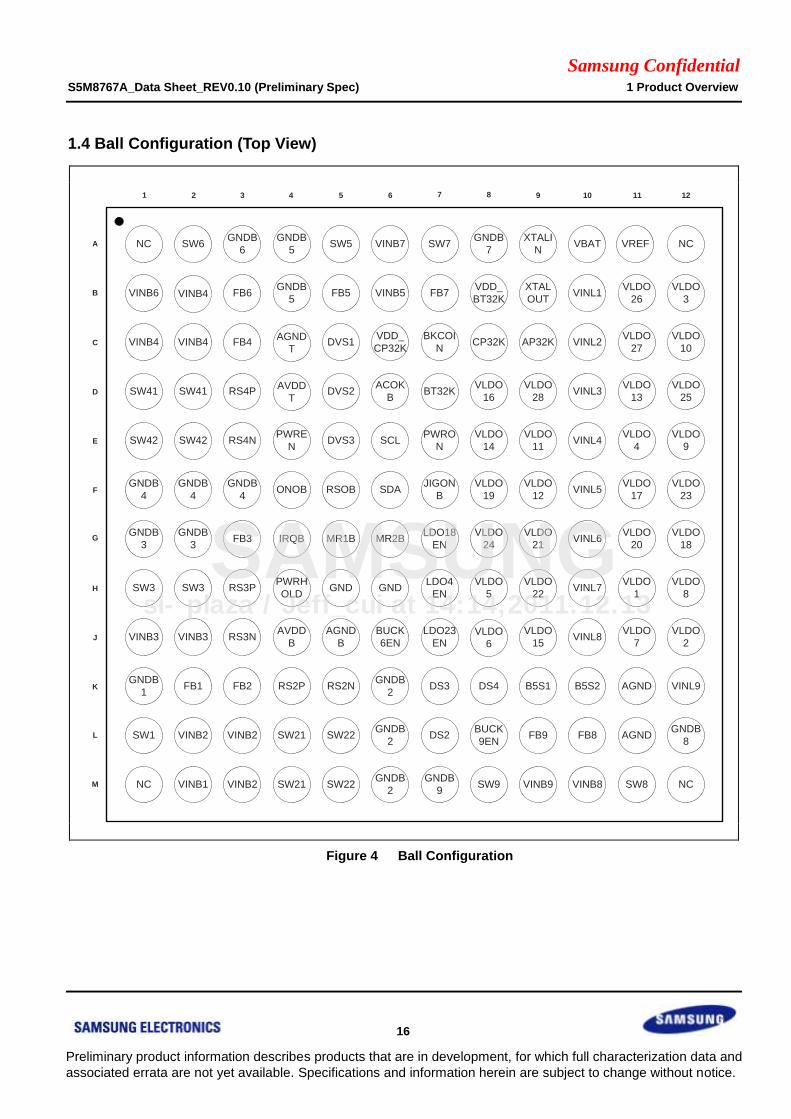
1.4 Ball Configuration (Top View)
A
B
C
D
E
F
G
H
J
K
L
1 2 3 4 5 6 7 8 9 10 11
NC SW6GNDB
6
GNDB
5SW5 VINB7 SW7
GNDB
7
XTALI
NNC
VINB6GNDB
5FB5 VINB5 FB7
VDD_
BT32K
XTAL
OUT
VLDO
10VINB4 VINB4
GND
BKCOI
N
VDD_
CP32KCP32K AP32K
VLDO
3
SW41 SW41 RS4P
GND
BT32KVLDO
16
VLDO
28
VLDO
25
SW42 SW42PWRE
N
RSOB
IRQB
SCLVLDO
14
VLDO
11
VLDO
9
GNDB
4
GNDB
4ONOB
JIGON
BSDA
VLDO
19
VLDO
12
VLDO
23
GNDB
3
GNDB
3
RS3P
ACOK
B
PWRH
OLD
MR1B MR2BVLDO
24
VLDO
21
VLDO
18
SW3 SW3
FB3
BUCK
6EN
LDO23
EN
B5S2
VLDO
5
VLDO
22
VLDO
8
VINB3 VINB3AVDD
BRS3N
DVS3
RS2P
VLDO
15
VLDO
2
GNDB
1
AGND
B
RS2NFB2 DS4 VINL9
SW1
FB1
VINB2 SW21 SW22GNDB
2DS2 FB9
DS3
GNDB
8
NC VINB1 VINB2 SW21 SW22GNDB
2
GNDB
9SW9 VINB9 NC
12
M
VLDO
26
VLDO
27
VLDO
13
VLDO
4
VLDO
17
VLDO
20
VLDO
1
VLDO
7
AGND
AGND
SW8
VINL1
VINL2
VINL3
VINL4
VINL5
VINL6
VINL7
VINL8
B5S1
FB8
VINB8
VLDO
6
VBAT VREF
AGND
T
FB6VINB4
AVDD
T
FB4
RS4N
GNDB
4
VINB2
LDO18
EN
LDO4
EN
GNDB
2
BUCK
9EN
DVS1
DVS2
PWRO
N
Figure 4 Ball Configuration
si-plaza / Jeff_cui at 14:14,2011.12.13
SAMSUNG

Samsung Confidential S5M8767A_Data Sheet_REV0.10 (Preliminary Spec) 1 Product Overview
17
Preliminary product information describes products that are in development, for which full characterization data and
associated errata are not yet available. Specifications and information herein are subject to change without notice.
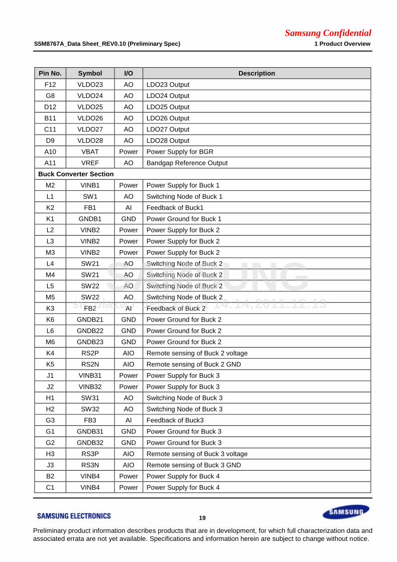
1.5 Ball Description
Pin No. Symbol I/O Description
Power Management and I2C Section
A9 XTALIN AI 32.768 kHz Crystal Oscillator Input. Connect 22 pF
B8 VDD_BT32K Power Power Supply for 32.768 kHz BT Buffer
B9 XTALOUT AO 32.768 kHz Crystal Oscillator Output. Connect 22 pF
C4 AGNDT GND Analog Ground for Bucks.
C6 VDD_CP32K Power Power Supply for 32.768 kHz CP Buffer
C7 BKCOIN AO Back up Battery Charger Output
C8 CP32K DO 32.768 kHz Output for CP
C9 AP32K DO 32.768 kHz Output for AP
D4 AVDDT Power Power Supply for Bucks.
D6 ACOKB DI VDCIN okay signal from external charger
D7 BT32K DO 32.768 kHz Output for BT
E4 PWREN DI Power Enable Pin for Buck2/3/4 and LDO2/6/7/8/10/11/12/14/15/16
E6 SCL DI I2C Serial Clock Input
E7 PWRON DI Power Enable Signal. Connected 800 k Pull-down to Ground.
F4 ONOB DO PWRON key active low signal. NMOS Open Drain
F5 RSOB DO Reset Output. NMOS Open Drain
F6 SDA DIO I2C Serial Data Bidirectional
F7 JIGONB DI Power Enable Signal through JIG.
G4 IRQB DO Interrupt Request Output (active low). NMOS Open Drain
G5 MR1B DI Manual Reset Input 1
G6 MR2B DI Manual Reset Input 2
G7 LDO18EN DI LDO18 Enable
H4 PWRHOLD DI Power Supply Hold Signal
H5 GND GND Ground
H6 GND GND Ground
H7 LDO4EN DI LDO4 Enable
J4 AVDDB Power Power Supply for Bucks.
J5 AGNDB GND Analog Ground for Bucks.
J6 BUCK6EN DI BUCK 6 Enable
J7 LDO23EN DI LDO23 Enable
K9 B5S1 DI Set the Buck 5 & LDO2 default voltage.
K10 B5S2 DI Set the Buck 5 & LDO2 default voltage.
K11 AGND GND Analog Ground
L8 BUCK9EN DI BUCK 9 Enable
si-plaza / Jeff_cui at 14:14,2011.12.13
SAMSUNG

Samsung Confidential S5M8767A_Data Sheet_REV0.10 (Preliminary Spec) 1 Product Overview
18
Preliminary product information describes products that are in development, for which full characterization data and
associated errata are not yet available. Specifications and information herein are subject to change without notice.
Pin No. Symbol I/O Description
L11 AGND GND Analog Ground
A1 NC AIO No Connection
A12 NC AIO No Connection
M1 NC AIO No Connection
M12 NC AIO No Connection
LDO Regulator, BGR Section
B10 VINL1 Power Power Supply for LDO3/10/26/27 from Buck 7 or VBAT
C10 VINL2 Power Power Supply for LDO13/16/25/28 from Buck 7 or VBAT
D10 VINL3 Power Power Supply for LDO11/14 from Buck7 or VBAT
E10 VINL4 Power Power Supply for LDO4/9
F10 VINL5 Power Power Supply for LDO12/17/19/23
G10 VINL6 Power Power Supply for LDO18/20/21/24
H10 VINL7 Power Power Supply for LDO5/22
J10 VINL8 Power Power Supply for LDO1/6/7/8/15 from Buck 8 or VBAT
K12 VINL9 Power Power Supply for LDO2 from Buck 8 or VBAT
H11 VLDO1 AO LDO1 Output
J12 VLDO2 AO LDO2 Output
B12 VLDO3 AO LDO3 Output
E11 VLDO4 AO LDO4 Output
H8 VLDO5 AO LDO5 Output
J8 VLDO6 AO LDO6 Output
J11 VLDO7 AO LDO7 Output
H12 VLDO8 AO LDO8 Output
E12 VLDO9 AO LDO9 Output
C12 VLDO10 AO LDO10 Output
E9 VLDO11 AO LDO11 Output
F9 VLDO12 AO LDO12 Output
D11 VLDO13 AO LDO13 Output
E8 VLDO14 AO LDO14 Output
J9 VLDO15 AO LDO15 Output
D8 VLDO16 AO LDO16 Output
F11 VLDO17 AO LDO17 Output
G12 VLDO18 AO LDO18 Output
F8 VLDO19 AO LDO19 Output
G11 VLDO20 AO LDO20 Output
G9 VLDO21 AO LDO21 Output
H9 VLDO22 AO LDO22 Output
si-plaza / Jeff_cui at 14:14,2011.12.13
SAMSUNG
Samsung Confidential S5M8767A_Data Sheet_REV0.10 (Preliminary Spec) 1 Product Overview
19
Preliminary product information describes products that are in development, for which full characterization data and
associated errata are not yet available. Specifications and information herein are subject to change without notice.
Pin No. Symbol I/O Description
F12 VLDO23 AO LDO23 Output
G8 VLDO24 AO LDO24 Output
D12 VLDO25 AO LDO25 Output
B11 VLDO26 AO LDO26 Output
C11 VLDO27 AO LDO27 Output
D9 VLDO28 AO LDO28 Output
A10 VBAT Power Power Supply for BGR
A11 VREF AO Bandgap Reference Output
Buck Converter Section
M2 VINB1 Power Power Supply for Buck 1
L1 SW1 AO Switching Node of Buck 1
K2 FB1 AI Feedback of Buck1
K1 GNDB1 GND Power Ground for Buck 1
L2 VINB2 Power Power Supply for Buck 2
L3 VINB2 Power Power Supply for Buck 2
M3 VINB2 Power Power Supply for Buck 2
L4 SW21 AO Switching Node of Buck 2
M4 SW21 AO Switching Node of Buck 2
L5 SW22 AO Switching Node of Buck 2
M5 SW22 AO Switching Node of Buck 2
K3 FB2 AI Feedback of Buck 2
K6 GNDB21 GND Power Ground for Buck 2
L6 GNDB22 GND Power Ground for Buck 2
M6 GNDB23 GND Power Ground for Buck 2
K4 RS2P AIO Remote sensing of Buck 2 voltage
K5 RS2N AIO Remote sensing of Buck 2 GND
J1 VINB31 Power Power Supply for Buck 3
J2 VINB32 Power Power Supply for Buck 3
H1 SW31 AO Switching Node of Buck 3
H2 SW32 AO Switching Node of Buck 3
G3 FB3 AI Feedback of Buck3
G1 GNDB31 GND Power Ground for Buck 3
G2 GNDB32 GND Power Ground for Buck 3
H3 RS3P AIO Remote sensing of Buck 3 voltage
J3 RS3N AIO Remote sensing of Buck 3 GND
B2 VINB4 Power Power Supply for Buck 4
C1 VINB4 Power Power Supply for Buck 4
si-plaza / Jeff_cui at 14:14,2011.12.13
SAMSUNG

Samsung Confidential S5M8767A_Data Sheet_REV0.10 (Preliminary Spec) 1 Product Overview
20
Preliminary product information describes products that are in development, for which full characterization data and
associated errata are not yet available. Specifications and information herein are subject to change without notice.
Pin No. Symbol I/O Description
C2 VINB4 Power Power Supply for Buck 4
D1 SW41 AO Switching Node of Buck 4
D2 SW41 AO Switching Node of Buck 4
E1 SW42 AO Switching Node of Buck 4
E2 SW42 AO Switching Node of Buck 4
C3 FB4 AI Feedback of Buck 4
F1 GNDB41 GND Power Ground for Buck 4
F2 GNDB42 GND Power Ground for Buck 4
F3 GNDB43 GND Power Ground for Buck 4
D3 RS4P AIO Remote sensing of Buck 4 voltage
E3 RS4N AIO Remote sensing of Buck 4 GND
B6 VINB5 Power Power Supply for Buck 5
A5 SW5 AO Switching Node of Buck 5
B5 FB5 AIO Feedback of Buck 5
A4 GNDB51 GND Power Ground for Buck 5
B4 GNDB52 GND Power Ground for Buck 5
B1 VINB6 Power Power Supply for Buck 6
A2 SW6 AO Switching Node of Buck 6
B3 FB6 AI Feedback of Buck 6
A3 GNDB6 GND Power Ground for Buck 6
A6 VINB7 Power Power Supply for Buck 7
A7 SW7 AO Switching Node of Buck 7
B7 FB7 AI Feedback of Buck 7
A8 GNDB7 GND Power Ground for Buck 7
M10 VINB8 Power Power Supply for Buck 8
M11 SW8 AO Switching Node of Buck 8
L10 FB8 AI Feedback of Buck 8
L12 GNDB8 GND Power Ground for Buck 8
M9 VINB9 Power Power Supply for Buck 9
M8 SW9 AO Switching Node of Buck 9
L9 FB9 AI Feedback of Buck 9
M7 GNDB9 GND Power Ground for Buck 9
L7 DS2 DI DVS Selection for Buck 2
K7 DS3 DI DVS Selection for Buck 3
K8 DS4 DI DVS Selection for Buck 4
C5 DVS1 DI Output Voltage Setting for Buck2/3/4
D5 DVS2 DI Output Voltage Setting for Buck2/3/4
si-plaza / Jeff_cui at 14:14,2011.12.13
SAMSUNG

Samsung Confidential S5M8767A_Data Sheet_REV0.10 (Preliminary Spec) 1 Product Overview
21
Preliminary product information describes products that are in development, for which full characterization data and
associated errata are not yet available. Specifications and information herein are subject to change without notice.
Pin No. Symbol I/O Description
E5 DVS3 DI Output Voltage Setting for Buck2/3/4
NOTE: Power, GND: Power Supply.
AI, AO, AIO: Analog Input, Output, Input/Output.
DI, DO, DIO: Digital Input, Output, Input/Output.
si-plaza / Jeff_cui at 14:14,2011.12.13
SAMSUNG
Samsung Confidential S5M8767A_Data Sheet_REV0.10 (Preliminary Spec) 1 Product Overview
22
Preliminary product information describes products that are in development, for which full characterization data and
associated errata are not yet available. Specifications and information herein are subject to change without notice.
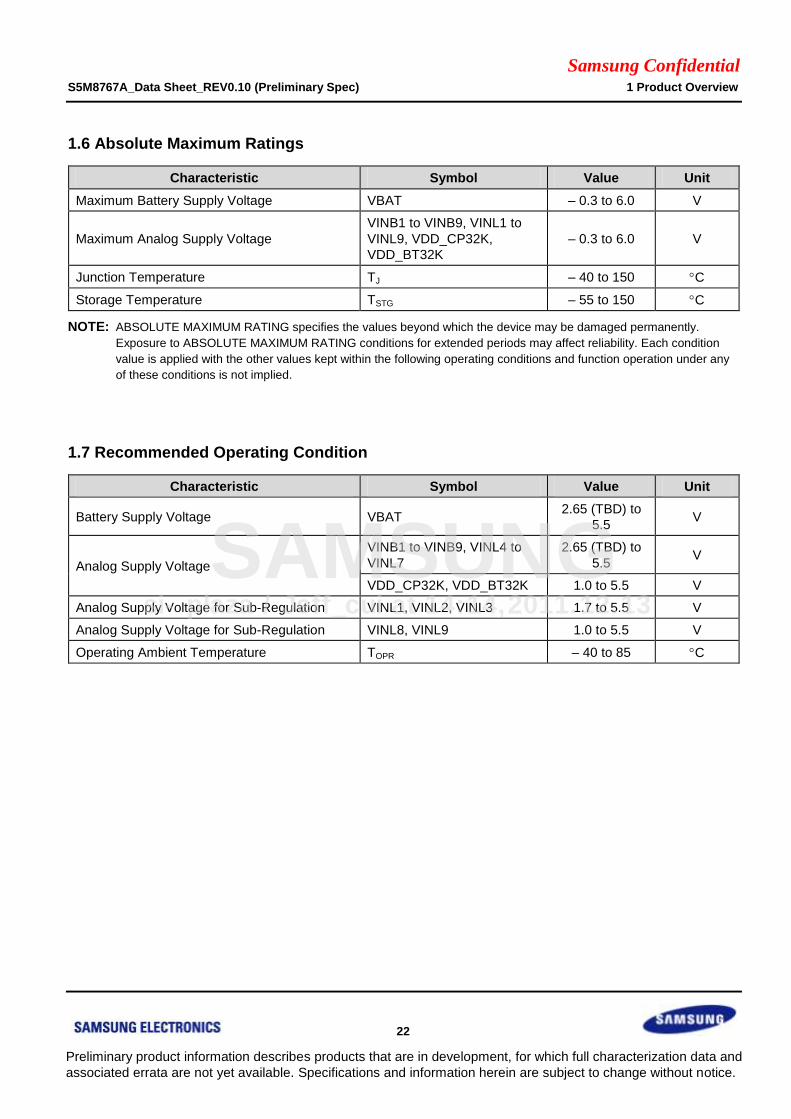
1.6 Absolute Maximum Ratings
Characteristic Symbol Value Unit
Maximum Battery Supply Voltage VBAT – 0.3 to 6.0 V
Maximum Analog Supply Voltage
VINB1 to VINB9, VINL1 to
VINL9, VDD_CP32K,
VDD_BT32K
– 0.3 to 6.0 V
Junction Temperature TJ – 40 to 150 C
Storage Temperature TSTG – 55 to 150 C
NOTE: ABSOLUTE MAXIMUM RATING specifies the values beyond which the device may be damaged permanently.
Exposure to ABSOLUTE MAXIMUM RATING conditions for extended periods may affect reliability. Each condition
value is applied with the other values kept within the following operating conditions and function operation under any
of these conditions is not implied.
1.7 Recommended Operating Condition
Characteristic Symbol Value Unit
Battery Supply Voltage VBAT 2.65 (TBD) to
5.5 V
Analog Supply Voltage
VINB1 to VINB9, VINL4 to
VINL7
2.65 (TBD) to
5.5 V
VDD_CP32K, VDD_BT32K 1.0 to 5.5 V
Analog Supply Voltage for Sub-Regulation VINL1, VINL2, VINL3 1.7 to 5.5 V
Analog Supply Voltage for Sub-Regulation VINL8, VINL9 1.0 to 5.5 V
Operating Ambient Temperature TOPR – 40 to 85 C
si-plaza / Jeff_cui at 14:14,2011.12.13
SAMSUNG
Samsung Confidential S5M8767A_Data Sheet_REV0.10 (Preliminary Spec) 2 Electrical Specifications
23
Preliminary product information describes products that are in development, for which full characterization data and
associated errata are not yet available. Specifications and information herein are subject to change without notice.
2 Electrical Specifications
2.1 General and Logic
(VBAT = 3.7 V, TA = 25 C, unless otherwise specified)
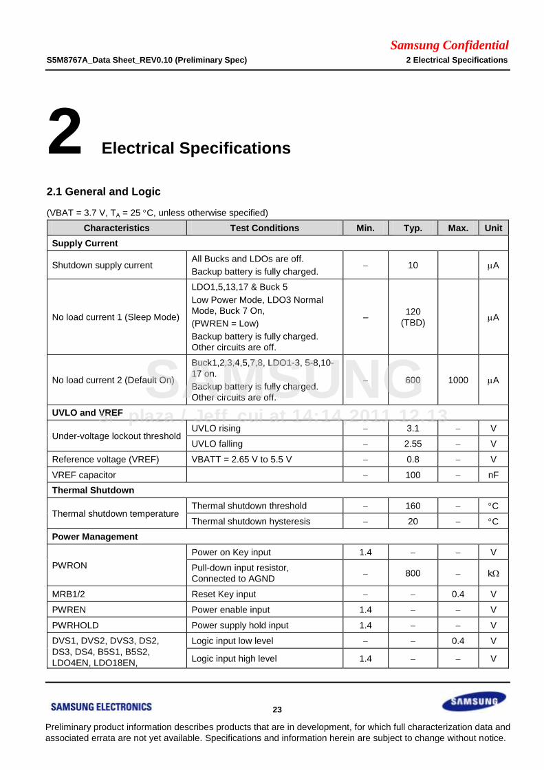
Characteristics Test Conditions Min. Typ. Max. Unit
Supply Current
Shutdown supply current All Bucks and LDOs are off.
Backup battery is fully charged. 10 A
No load current 1 (Sleep Mode)
LDO1,5,13,17 & Buck 5
Low Power Mode, LDO3 Normal
Mode, Buck 7 On,
(PWREN = Low)
Backup battery is fully charged.
Other circuits are off.
– 120
(TBD) A
No load current 2 (Default On)
Buck1,2,3,4,5,7,8, LDO1-3, 5-8,10-
17 on.
Backup battery is fully charged.
Other circuits are off.
600 1000 A
UVLO and VREF
Under-voltage lockout threshold UVLO rising 3.1 V
UVLO falling 2.55 V
Reference voltage (VREF) VBATT = 2.65 V to 5.5 V 0.8 V
VREF capacitor 100 nF
Thermal Shutdown
Thermal shutdown temperature Thermal shutdown threshold 160 C
Thermal shutdown hysteresis 20 C
Power Management
PWRON
Power on Key input 1.4 V
Pull-down input resistor,
Connected to AGND 800 k
MRB1/2 Reset Key input 0.4 V
PWREN Power enable input 1.4 V
PWRHOLD Power supply hold input 1.4 V
DVS1, DVS2, DVS3, DS2,
DS3, DS4, B5S1, B5S2,
LDO4EN, LDO18EN,
Logic input low level 0.4 V
Logic input high level 1.4 V
si-plaza / Jeff_cui at 14:14,2011.12.13
SAMSUNG
Samsung Confidential S5M8767A_Data Sheet_REV0.10 (Preliminary Spec) 2 Electrical Specifications
24
Preliminary product information describes products that are in development, for which full characterization data and
associated errata are not yet available. Specifications and information herein are subject to change without notice.
Characteristics Test Conditions Min. Typ. Max. Unit
LDO23EN, BUCK6EN,
BUCK9EN, JIGONB, ACOKB
SCL, SDA input
(I2C Control Signals)
Logic input low level from AP 0.4 V
Logic input high level from AP 1.4 V
Logic input hysteresis 0.2 V
Logic input coupling capacitor 10 pF
SDA Output (I2C Output Signal)
SDA logic output low signal,
NMOS open drain output, active low
Pull-up external resistor to
LDO3 V
Logic output to AP, active low 0.2 V
ONOB,RSOB, IRQB
System reset output signal,
NMOS open-drain output
Pull-up external resistor to
LDO3 V
Logic output to AP, active low 0.2 V
RSOB De-assert delay 60 ms
I2C Control
Clock frequency 3.5 MHz
Bus free time between start and
stop 1.3 s
Hold time repeated start
condition 0.6 s
CLK low period 1.3 s
si-plaza / Jeff_cui at 14:14,2011.12.13
SAMSUNG

Samsung Confidential S5M8767A_Data Sheet_REV0.10 (Preliminary Spec) 2 Electrical Specifications
25
Preliminary product information describes products that are in development, for which full characterization data and
associated errata are not yet available. Specifications and information herein are subject to change without notice.
2.2 Buck Converters
2.2.1 Buck Converter 1, 3, 5, 6, 7, 8, 9
(VBAT = 3.7 V, TA = 25 C, unless otherwise specified)
Buck 1, 3, and 5 to 9: Cout = 10 F, L = 1.0 H
Characteristics Test Conditions Min. Typ. Max. Unit
Voltage Mode Buck Converter
Input voltage range (1) 2.7 5.5 V
Shutdown current (2) Regulator disabled 0.1 A
Ground current (2)
Buck
1,3,5,6,
7,8,9
Regulator enabled, no load, no
switching, 17
A
Buck5 Low power mode 10
Output voltage range
Buck 1, programmable in 6.25 mV Steps 0.650 2.225
V
Buck 3, programmable in 6.25 mV Steps 0.600 1.6
Buck 5, programmable in 6.25 mV Steps 0.650 2.225
Buck 6, programmable in 6.25 mV Steps 0.650 2.225
Buck 7, programmable in 12.5 mV Steps 0.750 3.000
Buck 8, programmable in 12.5 mV Steps 0.750 3.000
Buck 9, programmable in 12.5 mV Steps 0.750 3.300
Default output voltage (5)
Buck 1 PWM Mode 3.0 % 1.0 + 3.0 %
V
Buck 3 PWM Mode 1.0 % 1.0 + 1.0 %
Buck 5
PWM Mode &
Iload < 5 mA
(Low power
mode)
B5S1 &
B5S2 (4)
00 3.0 % 1.2 + 3.0 %
01 3.0 % 1.35 + 3.0 %
10 3.0 % 1.50 + 3.0 %
11 3.0 % 1.80 + 3.0 %
Buck 6 PWM Mode 3.0 % 1.2 + 3.0 %
Buck 7 PWM Mode 3.0 % 2.0 + 3.0 %
Buck 8 PWM Mode 3.0 % 1.4 + 3.0 %
Buck 9 PWM Mode 3.0 % 2.85 + 3.0 %
Maximum output
current
Buck 1, 6, 7, 8, 9 1500
mA Buck 3 2500
Buck 5 Normal mode 2000
Low power mode 5
Output load regulation
Buck 1,
6, 7, 8,
9
10mA < Iout < 1.5 A (PWM) 0.15
%/A
Buck 3 10mA < Iout < 2.5 A (PWM) 0.15
Buck 5 10mA < Iout < 2.0 A (PWM) 0.15
si-plaza / Jeff_cui at 14:14,2011.12.13
SAMSUNG

Samsung Confidential S5M8767A_Data Sheet_REV0.10 (Preliminary Spec) 2 Electrical Specifications
26
Preliminary product information describes products that are in development, for which full characterization data and
associated errata are not yet available. Specifications and information herein are subject to change without notice.
Characteristics Test Conditions Min. Typ. Max. Unit
Output line regulation VINBx = 3.0 V to 4.5 V 0.1 %/V
Current limit
Buck 1 PFET Switch 2200
mA
Buck 3 PFET switch 3700
Buck 5 PFET switch 3000
Buck 6 PFET switch 2200
Buck 7,
8 PFET switch 2200
Buck 9 PFET switch 2200
On-resistance
Buck 1,
5, 6, 7,
8, 9
PFET switch (VINB to SW), ILX =
150 mA @3.7 V 150 -
m
NFET rectifier (SW to GNDB), ILX
= 150 mA @3.7 V 80 -
Buck 3
PFET switch (VINB to SW), ILX =
50 mA @3.7 V 130 -
NFET rectifier (SW to GNDB), ILX
= 150 mA @3.7 V 70 -
Switching frequency PWM mode 3.5 MHz
Active discharge
Regulator disabled, resistance from FB3 to
GNDB3 for Buck 3 0.1
k Regulator disabled, resistance from SWx to
GNDBx for Buck 1, 5, 6, 7, 8, 9 1
Soft start ramp rate (3) Ramp rate in soft start operation 30 mV/
s
Startup delay (3) Delay for calibration 20 s
Dynamic-change ramp
Rate (2) Buck 3
Positive and Negative Ramp Rate
in Dynamic Voltage Scale
5 mV/s,10 mV/s, 25 mV/s, 50
mV/s and 100 mV/s
Ramp off: Max ramp rate (100
mV)
5 10 100 mV/s
si-plaza / Jeff_cui at 14:14,2011.12.13
SAMSUNG
Samsung Confidential S5M8767A_Data Sheet_REV0.10 (Preliminary Spec) 2 Electrical Specifications
27
Preliminary product information describes products that are in development, for which full characterization data and
associated errata are not yet available. Specifications and information herein are subject to change without notice.
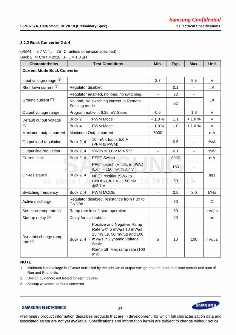
2.2.2 Buck Converter 2 & 4
(VBAT = 3.7 V, TA = 25 C, unless otherwise specified)
Buck 2, 4: Cout = 2x10 F, L = 1.0 H
Characteristics Test Conditions Min. Typ. Max. Unit
Current Mode Buck Converter
Input voltage range (1) 2.7 5.5 V
Shutdown current (2) Regulator disabled 0.1 A
Ground current (2)
Regulator enabled, no load, no switching, 22
A No load, No switching current In Remote
Sensing mode 32
Output voltage range Programmable in 6.25 mV Steps 0.6 1.6 V
Default output voltage (5)
Buck 2 PWM Mode 1.0 % 1.1 + 1.0 % V
Buck 4 PWM Mode 1.0 % 1.0 + 1.0 % V
Maximum output current Maximum Output current 5000 mA
Output load regulation Buck 2, 4 10 mA Iout 5.0 A
(PFM to PWM) 0.5 %/A
Output line regulation Buck 2, 4 VINBx = 3.0 V to 4.5 V 0.1 %/V
Current limit Buck 2, 4 PFET Switch 6000 mA
On-resistance Buck 2, 4
PFET switch (VINBx to SWx),
ILX = 150 mA @3.7 V 150
m NFET rectifier (SWx to
GNDBx), ILX = 150 mA
@3.7 V
80
Switching frequency Buck 2, 4 PWM MODE 2.5 3.0 MHz
Active discharge Regulator disabled, resistance from FBx to
GNDBx 50
Soft start ramp rate (3) Ramp rate in soft start operation 30 mV/s
Startup delay (3) Delay for calibration 20 s
Dynamic-change ramp
rate (2) Buck 2, 4
Positive and Negative Ramp
Rate with 5 mV/s,10 mV/s,
25 mV/s, 50 mV/s and 100
mV/s in Dynamic Voltage
Scale
Ramp off: Max ramp rate (100
mV)
5 10 100 mV/s
NOTE:
1. Minimum input voltage is 1/Dmax multiplied by the addition of output voltage and the product of load current and sum of
Ron and Rparasitic.
2. Design guidance; not tested for each device.
3. Startup waveform of Buck converter.
si-plaza / Jeff_cui at 14:14,2011.12.13
SAMSUNG
Samsung Confidential S5M8767A_Data Sheet_REV0.10 (Preliminary Spec) 2 Electrical Specifications
28
Preliminary product information describes products that are in development, for which full characterization data and
associated errata are not yet available. Specifications and information herein are subject to change without notice.
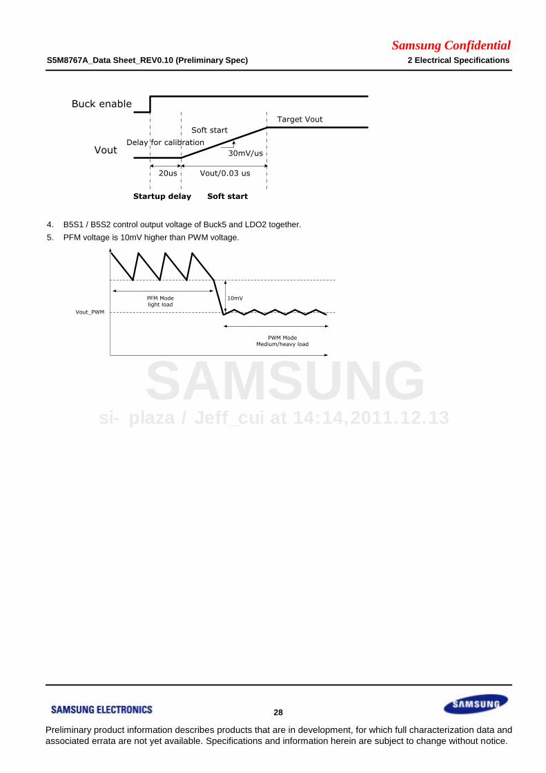
Buck enable
Vout
20us
30mV/us
Soft start
Delay for calibration
Target Vout
Vout/0.03 us
Startup delay Soft start
4. B5S1 / B5S2 control output voltage of Buck5 and LDO2 together.
5. PFM voltage is 10mV higher than PWM voltage.
PFM Mode light load
PWM Mode Medium/heavy load
Vout_PWM
10mV
si-plaza / Jeff_cui at 14:14,2011.12.13
SAMSUNG

Samsung Confidential S5M8767A_Data Sheet_REV0.10 (Preliminary Spec) 2 Electrical Specifications
29
Preliminary product information describes products that are in development, for which full characterization data and
associated errata are not yet available. Specifications and information herein are subject to change without notice.
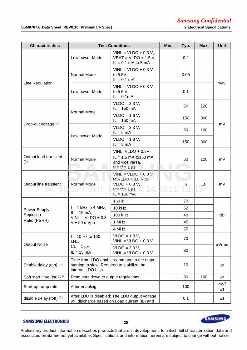
2.3 LDOs
2.3.1 LDO (P) 4, 5, 11, 12, 13, 14, 16, 17, 19, 20, 21, 22, 26, 27, 28 (150 mA, PMOS)
(VBAT = 3.7 V, TA = 25 C, unless otherwise specified)
Characteristics Test Conditions Min. Typ. Max. Unit
Input voltage range
(VINL) (1) 1.7 – 5.5 V
Under voltage Lockout Rising, 100 mV Hysteresis 1.6 1.7 V
Battery Voltage Range Equal or Higher than VINL 2.7 – 5.5 V
Output Voltage Range IL = 150 mA
Programmable in 50 mV steps 0.8 – 3.95 V
Default output voltage
(VLDO)
LDO (P) 4, 5, 11,
13, 14, 16, 26, 27,
28
150 mA @VINL
= VLDO +0.3V
1.8
V LDO (P) 17 2.8
LDO (P) 12, 19, 20,
21 3.0
LDO (P) 22 3.3
Maximum Load
Current
Normal Mode 150 mA
Low-Power Mode 5
Output Current Limit VOUT = 90 % of VLDO 180 225 270 mA
Minimum Output
Bypass Capacitance 0.7 1 F
Ground Current
Battery Supply
Current, with No
Load
Shutdown < 0.1
A
Normal Regulation 8 10
Low-Power Mode 0.5 1
Input Supply
Current, with No
Load
Shutdown 0 1
Normal Regulation 12 20
Low-Power Mode 2 5
Normal Mode Total Current 20 30
Low-Power Mode Total Current 2.5 6
LDO disabled Total Current < 0.1
Output voltage
accuracy
Normal Mode
VINL = VLDO + 0.3 V
to 5.5 V,
IL = 0.1 mA to 150 mA.
3 + 3
%
Low power Mode
VINL = VLDO + 0.3 V
to 5.5 V,
IL = 0.1 mA to 5 mA,
3 + 3
Load Regulation (2) Normal Mode
VINL = VLDO + 0.3 V,
VBAT = VLDO +1.5 V,
IL = 0.1 mA to 150 mA
0.1 %
si-plaza / Jeff_cui at 14:14,2011.12.13
SAMSUNG
Samsung Confidential S5M8767A_Data Sheet_REV0.10 (Preliminary Spec) 2 Electrical Specifications
30
Preliminary product information describes products that are in development, for which full characterization data and
associated errata are not yet available. Specifications and information herein are subject to change without notice.
Characteristics Test Conditions Min. Typ. Max. Unit
Low power Mode
VINL = VLDO + 0.3 V,
VBAT = VLDO + 1.5 V,
IL = 0.1 mA to 5 mA
0.2
Line Regulation
Normal Mode
VINL = VLDO + 0.3 V
to 5.5V,
IL = 0.1 mA
0.05
%/V
Low power Mode
VINL = VLDO + 0.3 V
to 5.5 V,
IL = 0.1mA
0.1
Drop-out voltage (2)
Normal Mode
VLDO = 3.3 V,
IL = 150 mA 60 120
mV
VLDO = 1.8 V,
IL = 150 mA 150 300
Low power Mode
VLDO = 3.3 V,
IL = 5 mA 50 100
VLDO = 1.8 V,
IL = 5 mA 150 300
Output load transient (2)
Normal Mode
VINL=VLDO + 0.3V
IL = 1.5 mA to150 mA,
and vice versa,
tr = tf = 1 µs
60 120 mV
Output line transient Normal Mode
VINL = VLDO + 0.3 V
to VLDO + 0.8 V to
VLDO + 0.3 V,
tr = tf = 1 µs,
IL = 150 mA
5 10 mV
Power Supply
Rejection
Ratio (PSRR)
f = 1 kHz to 4 MHz,
IL = 15 mA,
VINL = VLDO + 0.3
V + 50 mVpp
1 kHz 70
dB
10 kHz 62
100 kHz 40
1 MHz 45
4 MHz 55
Output Noise
f = 10 Hz to 100
kHz,
CL = 1 μF,
IL = 15 mA
VLDO = 1.8 V,
VINL = VLDO + 0.3 V 70
Vrms VLDO = 3.3 V,
VINL = VLDO + 0.3 V 80
Enable delay (ton) (3)
Time from LDO enable-command to the output
starting to slew. Required to stabilize the
internal LDO bias.
10 s
Soft start time (tsu) (3) From shut down to output regulations 30 100 s
Start-up ramp rate After enabling 100 mV/
s
disable delay (toff) (3) After LDO is disabled; The LDO output voltage
will discharge based on Load current (IL) and 0.1 s
si-plaza / Jeff_cui at 14:14,2011.12.13
SAMSUNG

Samsung Confidential S5M8767A_Data Sheet_REV0.10 (Preliminary Spec) 2 Electrical Specifications
31
Preliminary product information describes products that are in development, for which full characterization data and
associated errata are not yet available. Specifications and information herein are subject to change without notice.
Characteristics Test Conditions Min. Typ. Max. Unit
CL
Active Discharge
Resistance Output Disabled 0.05 0.08 0.15 k
Active Discharge Time
(tdis) (3) Until 10 % of VLDO 200 s
Transition time from
low power mode to
normal mode (tln), and
vice versa (tnl) (4)
IL = 1 mA 10 s
Clamp Active
Regulation Voltage (5) Clamp Active VLDO + 2.5 % V
Thermal shutdown Tj Rising. 165
C Tj Falling 150
si-plaza / Jeff_cui at 14:14,2011.12.13
SAMSUNG
Samsung Confidential S5M8767A_Data Sheet_REV0.10 (Preliminary Spec) 2 Electrical Specifications
32
Preliminary product information describes products that are in development, for which full characterization data and
associated errata are not yet available. Specifications and information herein are subject to change without notice.
2.3.2 LDO (P) 3, 10, 18, 23, 24, 25 (300 mA, PMOS)
(VBAT = 3.7 V, TA = 25 C, unless otherwise specified)
Characteristics Test Conditions Min. Typ. Max. Unit
Input voltage range
(VINL) (1) 1.7 5.5 V
Under voltage Lockout Rising, 100 mV Hysteresis 1.6 1.7 V
Battery Voltage Range Equal or Higher than VINL 2.7 – 5.5 V
Output Voltage Range IL = 300 mA
Programmable in 50 mV steps 0.8 – 3.95 V
Default output voltage
(VLDO)
LDO (P) 25
300 mA @VINL
= VLDO +0.3V
1.2
V LDO (P) 3, 10 1.8
LDO (P) 18, 23 2.8
LDO (P) 24 3.0
Maximum Load
Current
Normal Mode 300 mA
Low-Power Mode 5
Output Current Limit VOUT = 90 % of VLDO 350 500 750 mA
Minimum Output
Bypass Capacitance 1.5 2.2 F
Ground Current
Battery Supply
Current, with No
Load
Shutdown < 0.1
A
Normal Regulation 8 10
Low-Power Mode 0.5 1
Input Supply
Current, with No
Load
Shutdown 0 1
Normal Regulation 12 20
Low-Power Mode 2 5
Normal Mode Total Current 20 30
Low-Power Mode Total Current 2.5 6
LDO disabled Total Current < 0.1
Output voltage
accuracy
Normal Mode
VINL = VLDO + 0.3 V
to 5.5 V,
IL = 0.1 mA to 300 mA.
3 + 3
%
Low power Mode
VINL = VLDO + 0.3 V
to 5.5 V,
IL= 0.1 mA to 5 mA,
– 3 +3
Load Regulation (2)
Normal Mode
VINL = VLDO + 0.3 V,
VBAT = VLDO + 1.5 V,
IL = 0.1 mA to 300 mA
0.1
%
Low power Mode
VINL = VLDO + 0.3 V,
VBAT = VLDO + 1.5 V,
IL = 0.1 mA to 5 mA
0.2
Line Regulation Normal Mode VINL = VLDO + 0.3 V
to 5.5V, IL = 0.1 mA 0.05 %/V
si-plaza / Jeff_cui at 14:14,2011.12.13
SAMSUNG

Samsung Confidential S5M8767A_Data Sheet_REV0.10 (Preliminary Spec) 2 Electrical Specifications
33
Preliminary product information describes products that are in development, for which full characterization data and
associated errata are not yet available. Specifications and information herein are subject to change without notice.
Characteristics Test Conditions Min. Typ. Max. Unit
Low power Mode VINL = VLDO + 0.3 V
to 5.5 V, IL = 0.1 mA 0.1
Drop-out voltage (2)
Normal Mode
VLDO = 3.7 V,
IL = 300 mA 60 120
mV
VLDO = 1.8 V,
IL = 300 mA 150 300
Low power Mode
VLDO = 3.3 V,
IL = 5 mA 50 100
VLDO = 1.8 V,
IL = 5 mA 150 300
Output load transient (2)
Normal Mode
VINL=VLDO + 0.3V
IL = 1.5 mA to 300 mA,
and vice versa,
tr = tf = 1 µs
60 120 mV
Output line transient Normal Mode
VINL = VLDO + 0.3 V
to VLDO + 0.8 V to
VLDO + 0.3 V,
tr = tf = 1 µs,
IL = 300 mA
5 10 mV
Power Supply
Rejection
Ratio (PSRR)
f = 1 kHz to 4 MHz,
IL = 30 mA,
VINL= VLDO + 0.3
V + 50 mVpp
1 kHz 70
dB
10 kHz 62
100 kHz 40
1 MHz 45
4 MHz 55
Output Noise
f = 10 Hz to 100
kHz,
CL = 2.2 μF,
IL = 30 mA
VLDO = 1.8 V,
VINL= VLDO + 0.3 V 70
Vrms VLDO = 3.3 V,
VINL = VLDO + 0.3 V 100
Enable delay (ton) (3)
Time from LDO enable-command to the output
starting to slew. Required to stabilize the
internal LDO bias.
10 s
Soft start time (tsu) (3) From shut down to output regulations 30 100 s
Start-up ramp rate After enabling 150 mV/
s
disable delay (toff) (3)
After LDO is disabled; The LDO output voltage
will discharge based on Load current (IL) and
CL
0.1 s
Active Discharge
Resistance Output Disabled 0.05 0.08 0.15 k
Active Discharge Time
(tdis) (3) Until 10 % of VLDO 400 s
Transition time from
low power mode to IL = 1 mA 10 s
si-plaza / Jeff_cui at 14:14,2011.12.13
SAMSUNG
Samsung Confidential S5M8767A_Data Sheet_REV0.10 (Preliminary Spec) 2 Electrical Specifications
34
Preliminary product information describes products that are in development, for which full characterization data and
associated errata are not yet available. Specifications and information herein are subject to change without notice.
Characteristics Test Conditions Min. Typ. Max. Unit
normal mode (tln), and
vice versa (tnl) (4)
Clamp Active
Regulation Voltage (5) Clamp Active VLDO + 2.5 % V
Thermal shutdown Tj Rising. 165
C Tj Falling 150
si-plaza / Jeff_cui at 14:14,2011.12.13
SAMSUNG
Samsung Confidential S5M8767A_Data Sheet_REV0.10 (Preliminary Spec) 2 Electrical Specifications
35
Preliminary product information describes products that are in development, for which full characterization data and
associated errata are not yet available. Specifications and information herein are subject to change without notice.
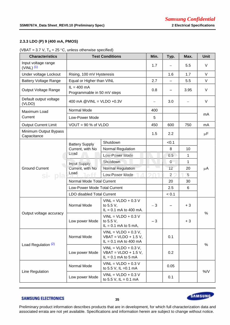
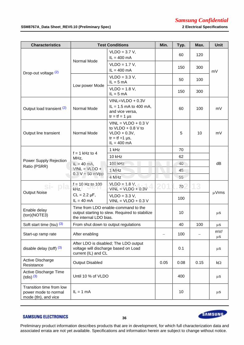
2.3.3 LDO (P) 9 (400 mA, PMOS)
(VBAT = 3.7 V, TA = 25 C, unless otherwise specified)
Characteristics Test Conditions Min. Typ. Max. Unit
Input voltage range
(VINL) (1) 1.7 5.5 V
Under voltage Lockout Rising, 100 mV Hysteresis 1.6 1.7 V
Battery Voltage Range Equal or Higher than VINL 2.7 – 5.5 V
Output Voltage Range IL = 400 mA
Programmable in 50 mV steps 0.8 – 3.95 V
Default output voltage
(VLDO) 400 mA @VINL = VLDO +0.3V 3.0 V
Maximum Load
Current
Normal Mode 400 mA
Low-Power Mode 5
Output Current Limit VOUT = 90 % of VLDO 450 600 750 mA
Minimum Output Bypass
Capacitance 1.5 2.2 F
Ground Current
Battery Supply
Current, with No
Load
Shutdown <0.1
A
Normal Regulation 8 10
Low-Power Mode 0.5 1
Input Supply
Current, with No
Load
Shutdown 0 1
Normal Regulation 12 20
Low-Power Mode 2 5
Normal Mode Total Current 20 30
Low-Power Mode Total Current 2.5 6
LDO disabled Total Current < 0.1
Output voltage accuracy
Normal Mode
VINL = VLDO + 0.3 V
to 5.5 V,
IL = 0.1 mA to 400 mA.
3 – + 3
%
Low power Mode
VINL = VLDO + 0.3 V
to 5.5 V,
IL = 0.1 mA to 5 mA,
– 3 + 3
Load Regulation (2)
Normal Mode
VINL = VLDO + 0.3 V,
VBAT = VLDO + 1.5 V,
IL = 0.1 mA to 400 mA
0.1
%
Low power Mode
VINL = VLDO + 0.3 V,
VBAT = VLDO + 1.5 V,
IL = 0.1 mA to 5 mA
0.2
Line Regulation
Normal Mode VINL = VLDO + 0.3 V
to 5.5 V, IL =0.1 mA 0.05
%/V
Low power Mode VINL = VLDO + 0.3 V
to 5.5 V, IL = 0.1 mA 0.1
si-plaza / Jeff_cui at 14:14,2011.12.13
SAMSUNG
Samsung Confidential S5M8767A_Data Sheet_REV0.10 (Preliminary Spec) 2 Electrical Specifications
36
Preliminary product information describes products that are in development, for which full characterization data and
associated errata are not yet available. Specifications and information herein are subject to change without notice.
Characteristics Test Conditions Min. Typ. Max. Unit
Drop-out voltage (2)
Normal Mode
VLDO = 3.7 V,
IL = 400 mA 60 120
mV
VLDO = 1.7 V,
IL = 400 mA 150 300
Low power Mode
VLDO = 3.3 V,
IL = 5 mA 50 100
VLDO = 1.8 V,
IL = 5 mA 150 300
Output load transient (2) Normal Mode
VINL=VLDO + 0.3V
IL = 1.5 mA to 400 mA,
and vice versa,
tr = tf = 1 µs
60 100 mV
Output line transient Normal Mode
VINL = VLDO + 0.3 V
to VLDO + 0.8 V to
VLDO + 0.3V,
tr = tf =1 µs,
IL = 400 mA
5 10 mV
Power Supply Rejection
Ratio (PSRR)
f = 1 kHz to 4
MHz,
IL = 40 mA,
VINL = VLDO +
0.3 V + 50 mVpp
1 kHz 70
dB
10 kHz 62
100 kHz 40
1 MHz 45
4 MHz 55
Output Noise
f = 10 Hz to 100
kHz,
CL = 2.2 μF,
IL = 40 mA
VLDO = 1.8 V,
VINL = VLDO + 0.3V 70
Vrms VLDO = 3.3 V,
VINL = VLDO + 0.3 V 100
Enable delay
(ton)(NOTE3)
Time from LDO enable-command to the
output starting to slew. Required to stabilize
the internal LDO bias.
10 s
Soft start time (tsu) (3) From shut down to output regulations 40 100 s
Start-up ramp rate After enabling 100 mV/
s
disable delay (toff) (3)
After LDO is disabled; The LDO output
voltage will discharge based on Load
current (IL) and CL
0.1 s
Active Discharge
Resistance Output Disabled 0.05 0.08 0.15 k
Active Discharge Time
(tdis) (3) Until 10 % of VLDO 400 s
Transition time from low
power mode to normal
mode (tln), and vice
IL = 1 mA 10 s
si-plaza / Jeff_cui at 14:14,2011.12.13
SAMSUNG
Samsung Confidential S5M8767A_Data Sheet_REV0.10 (Preliminary Spec) 2 Electrical Specifications
37
Preliminary product information describes products that are in development, for which full characterization data and
associated errata are not yet available. Specifications and information herein are subject to change without notice.
Characteristics Test Conditions Min. Typ. Max. Unit
versa (tnl) (4)
Clamp Active Regulation
Voltage (5) Clamp Active VLDO + 2.5 % V
Thermal shutdown Tj Rising. 165
C Tj Falling 150
si-plaza / Jeff_cui at 14:14,2011.12.13
SAMSUNG

Samsung Confidential S5M8767A_Data Sheet_REV0.10 (Preliminary Spec) 2 Electrical Specifications
38
Preliminary product information describes products that are in development, for which full characterization data and
associated errata are not yet available. Specifications and information herein are subject to change without notice.
2.3.4 LDO (N) 1, 6, 7, 15 (150 mA, NMOS)
(VBAT = 3.7 V, TA = 25 C, unless otherwise specified)
Characteristics Test Conditions Min. Typ. Max. Unit
Input voltage range
(VINL) (1) VLDO VBAT V
Battery Voltage Range Equal or Higher than VINL 2.7 – 5.5 V
Output Voltage Range IL = 150 mA
Programmable in 25 mV steps 0.8 – 2.375 V
Default output voltage
(VLDO)
LDO (P) 1, 6, 7,
15
150 mA @VINL
= VLDO + 0.3V 1.0 V
Maximum Load
Current
Normal Mode 150 mA
Low-Power Mode 5
Output Current Limit VOUT = 90 % of VLDO 180 225 270 mA
Minimum Output Bypass
Capacitance 0.7 1 F
Ground Current
Battery Supply
Current, with No
Load
Shutdown < 0.1
A
Normal Regulation 28 40
Low-Power Mode 2 3
Input Supply
Current, with No
Load
Shutdown 0 1
Normal Regulation 2 5
Low-Power Mode 0 1
Normal Mode Total Current 30 45
Low-Power Mode Total Current 2 4
LDO disabled Total Current < 0.1
Output voltage accuracy
Normal Mode
VINL = VLDO + 0.3 V
to 5.5 V,
IL = 0.1 mA to 150 mA.
3 + 3
%
Low power Mode
VINL = VLDO + 0.3 V
to 5.5 V,
IL= 0.1 mA to 5 mA,
3 +3
Load Regulation (2)
Normal Mode
VINL = VLDO + 0.3 V,
VBAT = VLDO + 1.5 V,
IL= 0.1 mA to 150 mA
0.1
%
Low power Mode
VINL = VLDO + 0.3 V,
VBAT = VLDO + 1.5 V,
IL= 0.1 mA to 5 mA
0.2
Line Regulation
Normal Mode VINL = VLDO + 0.3 V
to 5.5 V, IL = 0.1 mA 0.05
%/V
Low power Mode
VBAT = VLDO + 0.3 V
to 5.5 V, IL = 0.1 mA
VINL = VLDO + 0.3 V
0.1
si-plaza / Jeff_cui at 14:14,2011.12.13
SAMSUNG
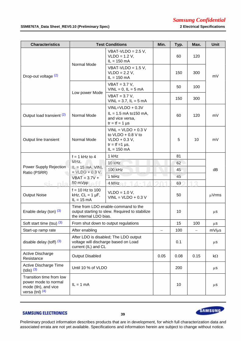
Samsung Confidential S5M8767A_Data Sheet_REV0.10 (Preliminary Spec) 2 Electrical Specifications
39
Preliminary product information describes products that are in development, for which full characterization data and
associated errata are not yet available. Specifications and information herein are subject to change without notice.
Characteristics Test Conditions Min. Typ. Max. Unit
Drop-out voltage (2)
Normal Mode
VBAT-VLDO = 2.5 V,
VLDO = 1.2 V,
IL = 150 mA
60 120
mV
VBAT-VLDO = 1.5 V,
VLDO = 2.2 V,
IL = 150 mA
150 300
Low power Mode
VBAT = 3.7 V,
VINL = 0, IL = 5 mA 50 100
VBAT = 3.7 V,
VINL = 3.7, IL = 5 mA 150 300
Output load transient (2) Normal Mode
VINL=VLDO + 0.3V
IL = 1.5 mA to150 mA,
and vice versa,
tr = tf = 1 µs
60 120 mV
Output line transient Normal Mode
VINL = VLDO + 0.3 V
to VLDO + 0.8 V to
VLDO + 0.3 V,
tr = tf =1 µs,
IL = 150 mA
5 10 mV
Power Supply Rejection
Ratio (PSRR)
f = 1 kHz to 4
MHz,
IL = 15 mA, VINL
= VLDO + 0.3 V,
VBAT = 3.7V +
50 mVpp
1 kHz 81
dB
10 kHz 62
100 kHz 45
1 MHz 45
4 MHz 69
Output Noise
f = 10 Hz to 100
kHz, CL = 1 μF,
IL = 15 mA
VLDO = 1.0 V,
VINL = VLDO + 0.3 V 50 Vrms
Enable delay (ton) (3)
Time from LDO enable-command to the
output starting to slew. Required to stabilize
the internal LDO bias.
10 s
Soft start time (tsu) (3) From shut down to output regulations 15 100 s
Start-up ramp rate After enabling 100 mV/s
disable delay (toff) (3)
After LDO is disabled; The LDO output
voltage will discharge based on Load
current (IL) and CL
0.1 s
Active Discharge
Resistance Output Disabled 0.05 0.08 0.15 k
Active Discharge Time
(tdis) (3) Until 10 % of VLDO 200 s
Transition time from low
power mode to normal
mode (tln), and vice
versa (tnl) (4)
IL = 1 mA 10 s
si-plaza / Jeff_cui at 14:14,2011.12.13
SAMSUNG
Samsung Confidential S5M8767A_Data Sheet_REV0.10 (Preliminary Spec) 2 Electrical Specifications
40
Preliminary product information describes products that are in development, for which full characterization data and
associated errata are not yet available. Specifications and information herein are subject to change without notice.
Characteristics Test Conditions Min. Typ. Max. Unit
Clamp Active Regulation
Voltage (5) Clamp Active VLDO + 2.5 % V
Thermal shutdown Tj Rising. 165
C Tj Falling 150
si-plaza / Jeff_cui at 14:14,2011.12.13
SAMSUNG
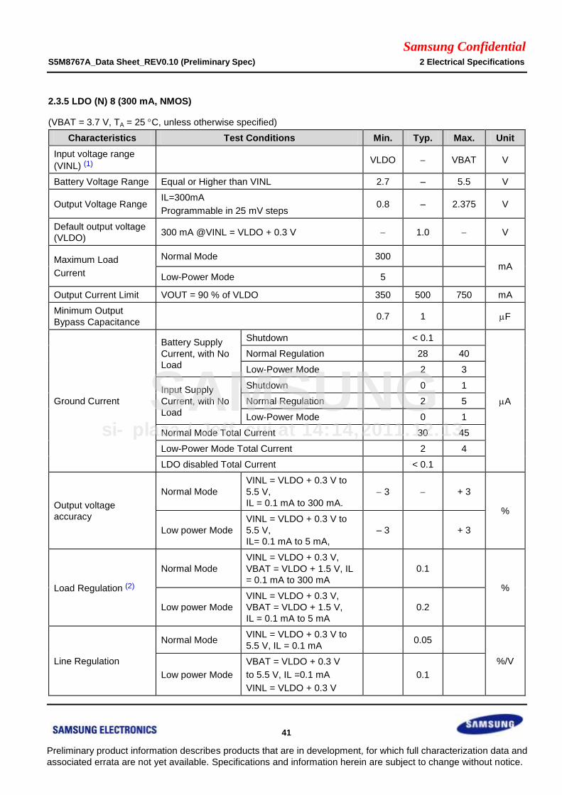
Samsung Confidential S5M8767A_Data Sheet_REV0.10 (Preliminary Spec) 2 Electrical Specifications
41
Preliminary product information describes products that are in development, for which full characterization data and
associated errata are not yet available. Specifications and information herein are subject to change without notice.
2.3.5 LDO (N) 8 (300 mA, NMOS)
(VBAT = 3.7 V, TA = 25 C, unless otherwise specified)
Characteristics Test Conditions Min. Typ. Max. Unit
Input voltage range
(VINL) (1) VLDO VBAT V
Battery Voltage Range Equal or Higher than VINL 2.7 – 5.5 V
Output Voltage Range IL=300mA
Programmable in 25 mV steps 0.8 – 2.375 V
Default output voltage
(VLDO) 300 mA @VINL = VLDO + 0.3 V 1.0 V
Maximum Load
Current
Normal Mode 300 mA
Low-Power Mode 5
Output Current Limit VOUT = 90 % of VLDO 350 500 750 mA
Minimum Output
Bypass Capacitance 0.7 1 F
Ground Current
Battery Supply
Current, with No
Load
Shutdown < 0.1
A
Normal Regulation 28 40
Low-Power Mode 2 3
Input Supply
Current, with No
Load
Shutdown 0 1
Normal Regulation 2 5
Low-Power Mode 0 1
Normal Mode Total Current 30 45
Low-Power Mode Total Current 2 4
LDO disabled Total Current < 0.1
Output voltage
accuracy
Normal Mode
VINL = VLDO + 0.3 V to
5.5 V,
IL = 0.1 mA to 300 mA.
3 + 3
%
Low power Mode
VINL = VLDO + 0.3 V to
5.5 V,
IL= 0.1 mA to 5 mA,
– 3 + 3
Load Regulation (2)
Normal Mode
VINL = VLDO + 0.3 V,
VBAT = VLDO + 1.5 V, IL
= 0.1 mA to 300 mA
0.1
%
Low power Mode
VINL = VLDO + 0.3 V,
VBAT = VLDO + 1.5 V,
IL = 0.1 mA to 5 mA
0.2
Line Regulation
Normal Mode VINL = VLDO + 0.3 V to
5.5 V, IL = 0.1 mA 0.05
%/V
Low power Mode
VBAT = VLDO + 0.3 V
to 5.5 V, IL =0.1 mA
VINL = VLDO + 0.3 V
0.1
si-plaza / Jeff_cui at 14:14,2011.12.13
SAMSUNG

Samsung Confidential S5M8767A_Data Sheet_REV0.10 (Preliminary Spec) 2 Electrical Specifications
42
Preliminary product information describes products that are in development, for which full characterization data and
associated errata are not yet available. Specifications and information herein are subject to change without notice.
Characteristics Test Conditions Min. Typ. Max. Unit
Drop-out voltage (2)
Normal Mode
VBAT-VLDO = 2.5 V,
VLDO = 1.2 V,
IL = 300 mA
60 120
mV
VBAT-VLDO = 1.5 V,
VLDO = 2.2 V,
IL = 300 mA
150 300
Low power Mode
VBAT = 3.7 V, VINL = 0,
IL = 5 mA 50 100
VBAT = 3.7 V,
VINL = 3.7, IL = 5 mA 150 300
Output load transient (2)
Normal Mode
VINL=VLDO + 0.3V
IL = 1.5 mA to 300 mA,
and vice versa,
tr = tf = 1 µs
60 120 mV
Output line transient Normal Mode
VINL = VLDO + 0.3 V to
VLDO + 0.8 V to VLDO +
0.3 V,
tr = tf = 1 µs, IL = 300 mA
5 10 mV
Power Supply
Rejection
Ratio (PSRR)
f = 1 kHz to 4
MHz,
IL = 30 mA, VINL
= VLDO + 0.3 V,
VBAT = 3.7V +
50 mVpp
1 kHz 81
dB
10 kHz 62
100 kHz 45
1 MHz 45
4 MHz 55
Output Noise
f = 10 Hz to 100
kHz,
CL = 1 μF, IL =
30 mA
VLDO = 1.0 V, VINL =
VLDO + 0.3 V 50 Vrms
Enable delay (ton) (3)
Time from LDO enable-command to the output
starting to slew. Required to stabilize the
internal LDO bias.
10 s
Soft start time (tsu) (3) From shut down to output regulations 16 100 s
Start-up ramp rate After enabling 100 mV/
s
disable delay (toff) (3)
After LDO is disabled; The LDO output voltage
will discharge based on Load current (IL) and
CL
0.1 s
Active Discharge
Resistance Output Disabled 0.05 0.08 0.15 k
Active Discharge Time
(tdis) (3) Until 1 0 % of VLDO 200 s
Transition time from
low power mode to
normal mode (tln), and
IL = 1 mA 10 s
si-plaza / Jeff_cui at 14:14,2011.12.13
SAMSUNG

Samsung Confidential S5M8767A_Data Sheet_REV0.10 (Preliminary Spec) 2 Electrical Specifications
43
Preliminary product information describes products that are in development, for which full characterization data and
associated errata are not yet available. Specifications and information herein are subject to change without notice.
Characteristics Test Conditions Min. Typ. Max. Unit
vice versa (tnl) (4)
Clamp Active
Regulation Voltage (5) Clamp Active VLDO + 2.5 % V
Thermal shutdown Tj Rising. 165
C Tj Falling 150
si-plaza / Jeff_cui at 14:14,2011.12.13
SAMSUNG

Samsung Confidential S5M8767A_Data Sheet_REV0.10 (Preliminary Spec) 2 Electrical Specifications
44
Preliminary product information describes products that are in development, for which full characterization data and
associated errata are not yet available. Specifications and information herein are subject to change without notice.
2.3.6 LDO (N) 2 (450 mA, NMOS)
(VBAT = 3.7 V, TA = 25 C, unless otherwise specified)
Characteristics Test Conditions Min. Typ. Max. Unit
Input voltage range
(VINL) (1) VLDO VBAT V
Battery Voltage Range Equal or Higher than VINL 2.7 – 5.5 V
Output Voltage Range IL = 450 mA
Programmable in 25 mV steps 0.8 – 2.375 V
Default output voltage
(VLDO)
450 mA @VINL
= VLDO + 0.3V
B5S1 & B5S2 (6)
00 1.2
V 01 1.35
10 1.5
11 1.8
Maximum Load
Current
Normal Mode 450 mA
Low-Power Mode 5
Output Current Limit VOUT = 90 % of VLDO 495 765 1125 mA
Minimum Output Bypass
Capacitance 0.7 1 F
Ground Current
Battery Supply
Current, with No
Load
Shutdown < 0.1
A
Normal Regulation 28 40
Low-Power Mode 2 3
Input Supply
Current, with No
Load
Shutdown 0 1
Normal Regulation 2 5
Low-Power Mode 0 1
Normal Mode Total Current 30 45
Low-Power Mode Total Current 2 4
LDO disabled Total Current < 0.1
Output voltage accuracy
Normal Mode
VINL = VLDO + 0.3 V to
5.5 V,
IL = 0.1 mA to 450 mA.
3 + 3
%
Low power
Mode
VINL = VLDO + 0.3 V to
5.5 V,
IL = 0.1 mA to 5 mA,
– 3 + 3
Load Regulation (2)
Normal Mode
VINL = VLDO + 0.3 V,
VBAT = VLDO + 1.5 V,
IL = 0.1 mA to 450 mA
0.1
%
Low power
Mode
VINL = VLDO + 0.3 V,
VBAT = VLDO + 1.5 V,
IL = 0.1 mA to 5 mA
0.2
Line Regulation Normal Mode
VINL = VLDO + 0.3 V to
5.5 V, IL = 0.1 mA 0.05
%/V
Low power VBAT = VLDO + 0.3 V 0.1
si-plaza / Jeff_cui at 14:14,2011.12.13
SAMSUNG

Samsung Confidential S5M8767A_Data Sheet_REV0.10 (Preliminary Spec) 2 Electrical Specifications
45
Preliminary product information describes products that are in development, for which full characterization data and
associated errata are not yet available. Specifications and information herein are subject to change without notice.
Characteristics Test Conditions Min. Typ. Max. Unit
Mode to 5.5 V, IL =0.1 mA
VINL = VLDO + 0.3 V
Drop-out voltage (2)
Normal Mode
VBAT-VLDO = 2.5 V,
VLDO = 1.2 V,
IL = 450 mA
60 120
mV
VBAT-VLDO =1.5 V,
VLDO = 2.2 V,
IL = 450 mA
150 300
Low power
Mode
VBAT = 3.7 V, VINL = 0,
IL = 5 mA 50 100
VBAT = 3.7 V,
VINL = 3.7, IL= 5 mA 150 300
Output load transient (2) Normal Mode
VINL=VLDO + 0.3V
IL = 1.5 mA to 450 mA,
and vice versa,
tr = tf = 1 µs
60 120 mV
Output line transient Normal Mode
VINL = VLDO + 0.3 V to
VLDO + 0.8 V to VLDO +
0.3 V,
tr = tf = 1 µs,
IL = 450 mA
5 10 mV
Power Supply Rejection
Ratio (PSRR)
f = 1 kHz to 4
MHz,
IL = 45 mA,
VINL = VLDO +
0.3 V,
VBAT = 3.7V +
50 mVpp
1 kHz 81
dB
10 kHz 62
100 kHz 45
1 MHz 45
4 MHz 69
Output Noise
f = 10 Hz to 100
kHz, CL = 1 μF,
IL = 45 mA
VLDO = 1.2 V, VINL =
VLDO + 0.3 V 50 Vrms
Enable delay (ton) (3)
Time from LDO enable-command to the
output starting to slew. Required to stabilize
the internal LDO bias.
10 s
Soft start time (tsu) (3) From shut down to output regulations 16 100 s
Start-up ramp rate After enabling 100 mV/s
disable delay (toff) (3)
After LDO is disabled; The LDO output
voltage will discharge based on load current
(IL) and CL
0.1 s
Active Discharge
Resistance Output Disabled 0.05 0.08 0.15 k
Active Discharge Time
(tdis) (3) Until 10 % of VLDO 200 s
Transition time from low IL = 1 mA 10 s
si-plaza / Jeff_cui at 14:14,2011.12.13
SAMSUNG
Samsung Confidential S5M8767A_Data Sheet_REV0.10 (Preliminary Spec) 2 Electrical Specifications
46
Preliminary product information describes products that are in development, for which full characterization data and
associated errata are not yet available. Specifications and information herein are subject to change without notice.
Characteristics Test Conditions Min. Typ. Max. Unit
power mode to normal
mode (tln), and vice
versa (tnl) (4)
Clamp Active Regulation
Voltage (5) Clamp Active VLDO + 2.5 % V
Thermal shutdown Tj Rising. 165
C Tj Falling 150
NOTE:
1. Input voltage range is guaranteed from VLDOs + 0.3 V to 5.5 V.
2. Performance may be different by the effect of PCB layout and external components.
3. Enable and Disable timing diagram is shown as below:
90%
10%
LDO_EN
VLDO
ton
tsu toff
tdis
4. Transition waveforms from low-power mode to normal mode and vice versa are shown as below:
LPM
VLDO
tnl tln
Within ±3%
5. Over-voltage clamp operation is shown as below:
VLDO
Vnom*107.5%
Vnom*102.5%
t1 t2
t1: discharged by active current sink (80) and load current.
t2: discharged by bleeding resistor (PLDO: 750 k, NLDO: 1.1 M) and load current.
6. B5S1 / B5S2 control output voltage of Buck5 and LDO2 together.
2.4 Backup Coin Battery Charger
(VBATT = 3.7 V, TA = 25 C, unless otherwise specified)
Characteristics Test Conditions Min. Typ. Max. Unit
si-plaza / Jeff_cui at 14:14,2011.12.13
SAMSUNG
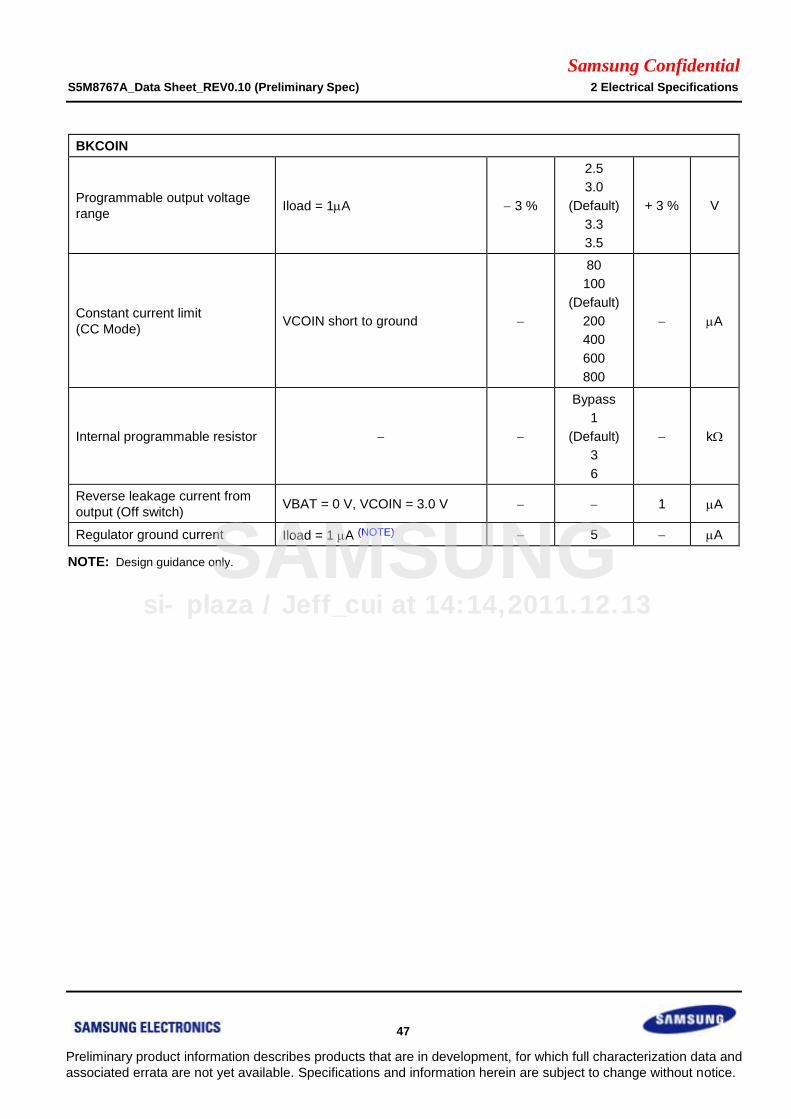
Samsung Confidential S5M8767A_Data Sheet_REV0.10 (Preliminary Spec) 2 Electrical Specifications
47
Preliminary product information describes products that are in development, for which full characterization data and
associated errata are not yet available. Specifications and information herein are subject to change without notice.
BKCOIN
Programmable output voltage
range Iload = 1A 3 %
2.5
3.0
(Default)
3.3
3.5
+ 3 % V
Constant current limit
(CC Mode) VCOIN short to ground
80
100
(Default)
200
400
600
800
A
Internal programmable resistor
Bypass
1
(Default)
3
6
k
Reverse leakage current from
output (Off switch) VBAT = 0 V, VCOIN = 3.0 V 1 A
Regulator ground current Iload = 1 A (NOTE) 5 A
NOTE: Design guidance only.
si-plaza / Jeff_cui at 14:14,2011.12.13
SAMSUNG
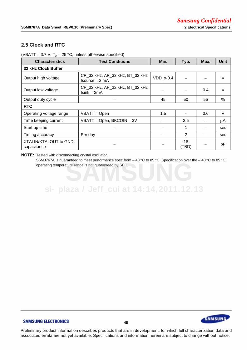
Samsung Confidential S5M8767A_Data Sheet_REV0.10 (Preliminary Spec) 2 Electrical Specifications
48
Preliminary product information describes products that are in development, for which full characterization data and
associated errata are not yet available. Specifications and information herein are subject to change without notice.
2.5 Clock and RTC
(VBATT = 3.7 V, TA = 25 C, unless otherwise specified)
Characteristics Test Conditions Min. Typ. Max. Unit
32 kHz Clock Buffer
Output high voltage CP_32 kHz, AP_32 kHz, BT_32 kHz
Isource = 2 mA VDD_x-0.4 V
Output low voltage CP_32 kHz, AP_32 kHz, BT_32 kHz
Isink = 2mA 0.4 V
Output duty cycle 45 50 55 %
RTC
Operating voltage range VBATT = Open 1.5 - 3.6 V
Time keeping current VBATT = Open, BKCOIN = 3V 2.5 A
Start up time 1 sec
Timing accuracy Per day 2 sec
XTALIN/XTALOUT to GND
capacitance
18
(TBD) pF
NOTE: Tested with disconnecting crystal oscillator.
S5M8767A is guaranteed to meet performance spec from – 40 C to 85 C. Specification over the – 40 C to 85 C
operating temperature range is not guaranteed by SEC.
si-plaza / Jeff_cui at 14:14,2011.12.13
SAMSUNG
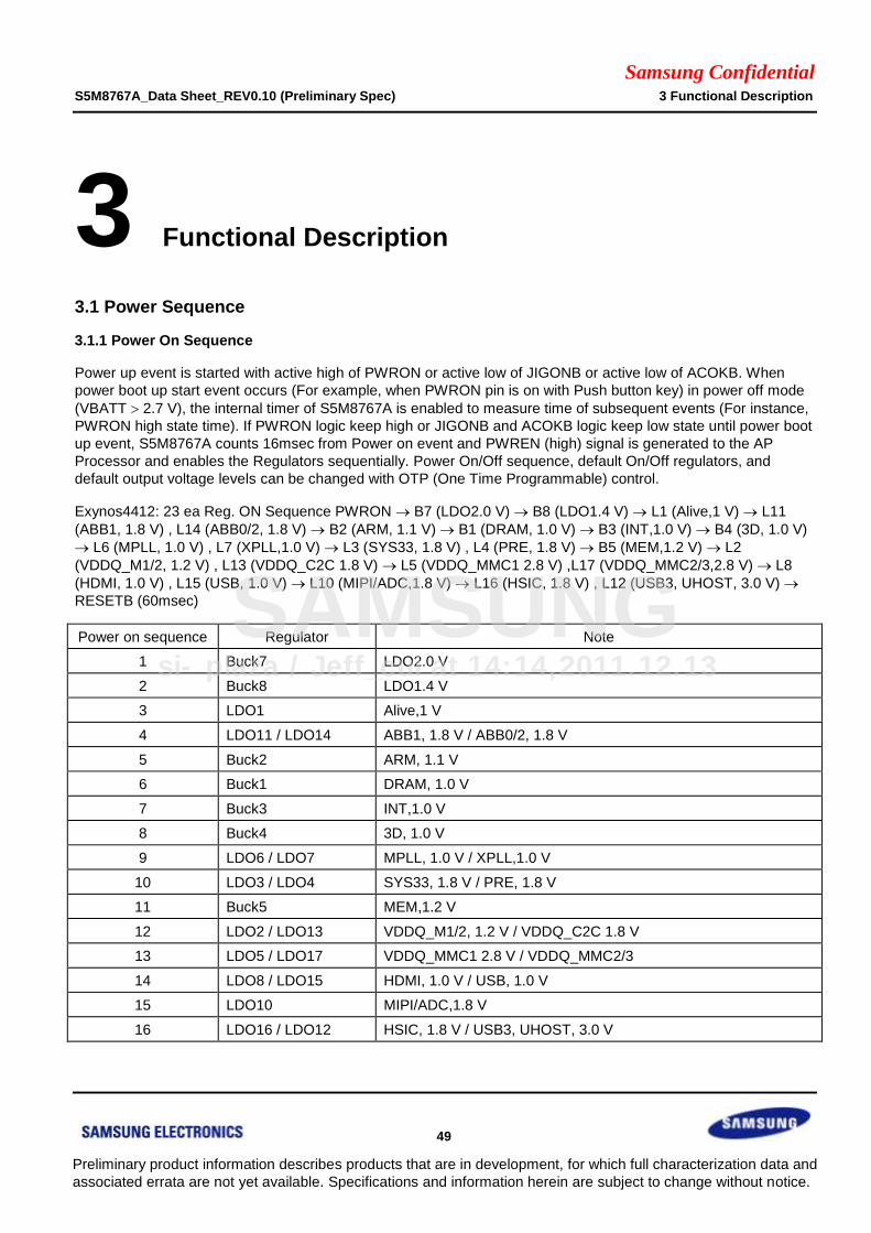
Samsung Confidential S5M8767A_Data Sheet_REV0.10 (Preliminary Spec) 3 Functional Description
49
Preliminary product information describes products that are in development, for which full characterization data and
associated errata are not yet available. Specifications and information herein are subject to change without notice.
3 Functional Description
3.1 Power Sequence
3.1.1 Power On Sequence
Power up event is started with active high of PWRON or active low of JIGONB or active low of ACOKB. When
power boot up start event occurs (For example, when PWRON pin is on with Push button key) in power off mode
(VBATT 2.7 V), the internal timer of S5M8767A is enabled to measure time of subsequent events (For instance,
PWRON high state time). If PWRON logic keep high or JIGONB and ACOKB logic keep low state until power boot
up event, S5M8767A counts 16msec from Power on event and PWREN (high) signal is generated to the AP
Processor and enables the Regulators sequentially. Power On/Off sequence, default On/Off regulators, and
default output voltage levels can be changed with OTP (One Time Programmable) control.
Exynos4412: 23 ea Reg. ON Sequence PWRON B7 (LDO2.0 V) B8 (LDO1.4 V) L1 (Alive,1 V) L11
(ABB1, 1.8 V) , L14 (ABB0/2, 1.8 V) B2 (ARM, 1.1 V) B1 (DRAM, 1.0 V) B3 (INT,1.0 V) B4 (3D, 1.0 V)
L6 (MPLL, 1.0 V) , L7 (XPLL,1.0 V) L3 (SYS33, 1.8 V) , L4 (PRE, 1.8 V) B5 (MEM,1.2 V) L2
(VDDQ_M1/2, 1.2 V) , L13 (VDDQ_C2C 1.8 V) L5 (VDDQ_MMC1 2.8 V) ,L17 (VDDQ_MMC2/3,2.8 V) L8
(HDMI, 1.0 V) , L15 (USB, 1.0 V) L10 (MIPI/ADC,1.8 V) L16 (HSIC, 1.8 V) , L12 (USB3, UHOST, 3.0 V)
RESETB (60msec)
Power on sequence Regulator Note
1 Buck7 LDO2.0 V
2 Buck8 LDO1.4 V
3 LDO1 Alive,1 V
4 LDO11 / LDO14 ABB1, 1.8 V / ABB0/2, 1.8 V
5 Buck2 ARM, 1.1 V
6 Buck1 DRAM, 1.0 V
7 Buck3 INT,1.0 V
8 Buck4 3D, 1.0 V
9 LDO6 / LDO7 MPLL, 1.0 V / XPLL,1.0 V
10 LDO3 / LDO4 SYS33, 1.8 V / PRE, 1.8 V
11 Buck5 MEM,1.2 V
12 LDO2 / LDO13 VDDQ_M1/2, 1.2 V / VDDQ_C2C 1.8 V
13 LDO5 / LDO17 VDDQ_MMC1 2.8 V / VDDQ_MMC2/3
14 LDO8 / LDO15 HDMI, 1.0 V / USB, 1.0 V
15 LDO10 MIPI/ADC,1.8 V
16 LDO16 / LDO12 HSIC, 1.8 V / USB3, UHOST, 3.0 V
si-plaza / Jeff_cui at 14:14,2011.12.13
SAMSUNG
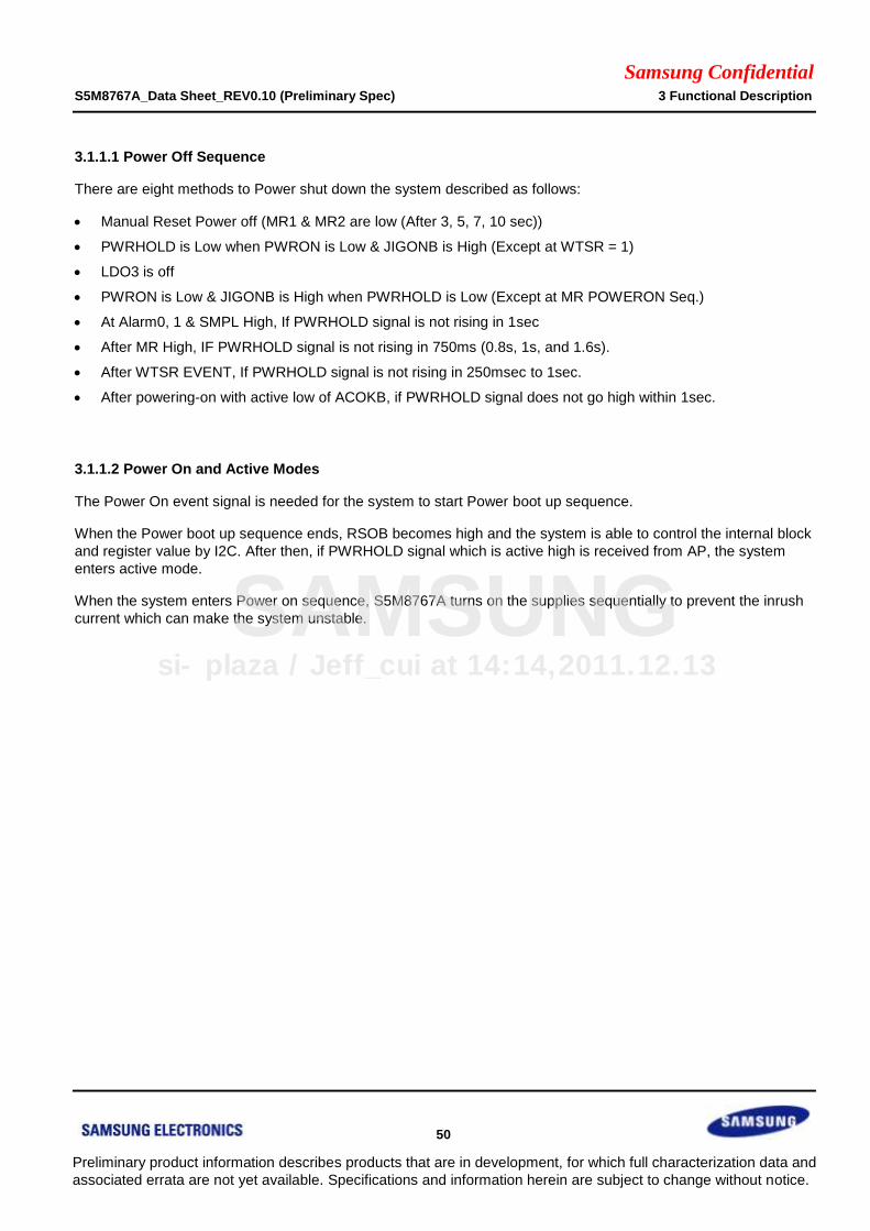
Samsung Confidential S5M8767A_Data Sheet_REV0.10 (Preliminary Spec) 3 Functional Description
50
Preliminary product information describes products that are in development, for which full characterization data and
associated errata are not yet available. Specifications and information herein are subject to change without notice.
3.1.1.1 Power Off Sequence
There are eight methods to Power shut down the system described as follows:
Manual Reset Power off (MR1 & MR2 are low (After 3, 5, 7, 10 sec))
PWRHOLD is Low when PWRON is Low & JIGONB is High (Except at WTSR = 1)
LDO3 is off
PWRON is Low & JIGONB is High when PWRHOLD is Low (Except at MR POWERON Seq.)
At Alarm0, 1 & SMPL High, If PWRHOLD signal is not rising in 1sec
After MR High, IF PWRHOLD signal is not rising in 750ms (0.8s, 1s, and 1.6s).
After WTSR EVENT, If PWRHOLD signal is not rising in 250msec to 1sec.
After powering-on with active low of ACOKB, if PWRHOLD signal does not go high within 1sec.
3.1.1.2 Power On and Active Modes
The Power On event signal is needed for the system to start Power boot up sequence.
When the Power boot up sequence ends, RSOB becomes high and the system is able to control the internal block
and register value by I2C. After then, if PWRHOLD signal which is active high is received from AP, the system
enters active mode.
When the system enters Power on sequence, S5M8767A turns on the supplies sequentially to prevent the inrush
current which can make the system unstable.
si-plaza / Jeff_cui at 14:14,2011.12.13
SAMSUNG
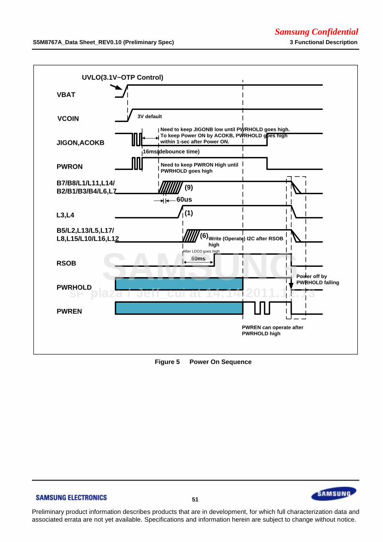
Samsung Confidential S5M8767A_Data Sheet_REV0.10 (Preliminary Spec) 3 Functional Description
51
Preliminary product information describes products that are in development, for which full characterization data and
associated errata are not yet available. Specifications and information herein are subject to change without notice.
VBAT
VCOIN
JIGON,ACOKB
PWRON
B7/B8/L1/L11,L14/
B2/B1/B3/B4/L6,L7
L3,L4
B5/L2,L13/L5,L17/
L8,L15/L10/L16,L12
RSOB
PWRHOLD
PWREN
UVLO(3.1V~OTP Control)
3V default
16ms(debounce time)
60us
(9)
(1)
(6)
60ms
Need to keep JIGONB low until PWRHOLD goes high.
To keep Power ON by ACOKB, PWRHOLD goes high
within 1-sec after Power ON.
Need to keep PWRON High until
PWRHOLD goes high
Write (Operate) I2C after RSOB
high
Power off by
PWRHOLD falling
PWREN can operate after
PWRHOLD high
After LDO3 goes high
Figure 5 Power On Sequence
si-plaza / Jeff_cui at 14:14,2011.12.13
SAMSUNG
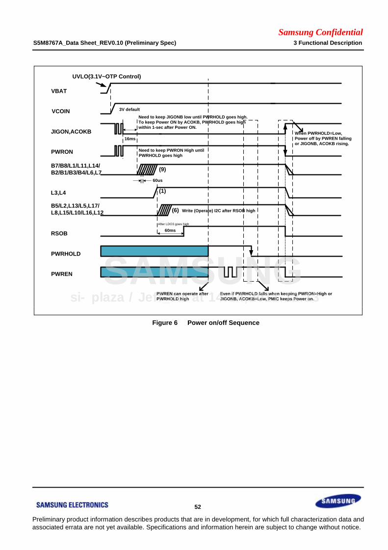
Samsung Confidential S5M8767A_Data Sheet_REV0.10 (Preliminary Spec) 3 Functional Description
52
Preliminary product information describes products that are in development, for which full characterization data and
associated errata are not yet available. Specifications and information herein are subject to change without notice.
VBAT
VCOIN
JIGON,ACOKB
PWRON
B7/B8/L1/L11,L14/
B2/B1/B3/B4/L6,L7
L3,L4
B5/L2,L13/L5,L17/
L8,L15/L10/L16,L12
RSOB
PWRHOLD
PWREN
UVLO(3.1V~OTP Control)
3V default
16ms
60us
(9)
(1)
(6)
60ms
Need to keep JIGONB low until PWRHOLD goes high.
To keep Power ON by ACOKB, PWRHOLD goes high
within 1-sec after Power ON.
Need to keep PWRON High until
PWRHOLD goes high
Write (Operate) I2C after RSOB high
PWREN can operate after
PWRHOLD high
Even if PWRHOLD falls when keeping PWRON=High or
JIGONB, ACOKB=Low, PMIC keeps Power on.
When PWRHOLD=Low,
Power off by PWREN falling
or JIGONB, ACOKB rising.
After LDO3 goes high
Figure 6 Power on/off Sequence
si-plaza / Jeff_cui at 14:14,2011.12.13
SAMSUNG
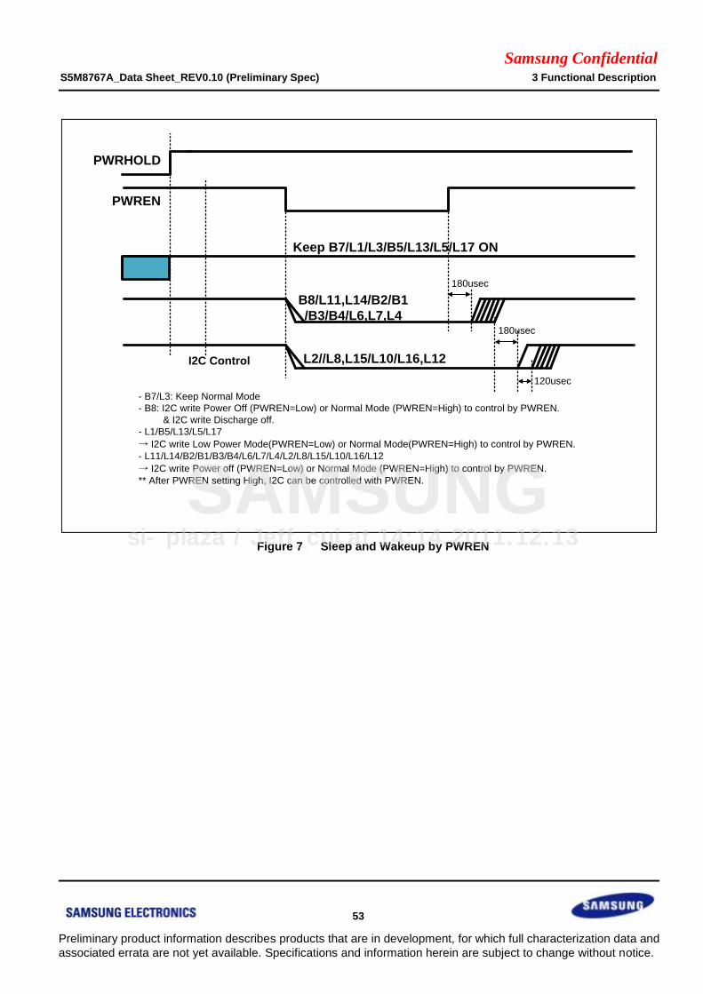
Samsung Confidential S5M8767A_Data Sheet_REV0.10 (Preliminary Spec) 3 Functional Description
53
Preliminary product information describes products that are in development, for which full characterization data and
associated errata are not yet available. Specifications and information herein are subject to change without notice.
PWREN
Keep B7/L1/L3/B5/L13/L5/L17 ON
B8/L11,L14/B2/B1
/B3/B4/L6,L7,L4
180usec
180usec
L2//L8,L15/L10/L16,L12I2C Control
- B7/L3: Keep Normal Mode
- B8: I2C write Power Off (PWREN=Low) or Normal Mode (PWREN=High) to control by PWREN.
& I2C write Discharge off.
- L1/B5/L13/L5/L17
→ I2C write Low Power Mode(PWREN=Low) or Normal Mode(PWREN=High) to control by PWREN.
- L11/L14/B2/B1/B3/B4/L6/L7/L4/L2/L8/L15/L10/L16/L12
→ I2C write Power off (PWREN=Low) or Normal Mode (PWREN=High) to control by PWREN.
** After PWREN setting High, I2C can be controlled with PWREN.
120usec
PWRHOLD
Figure 7 Sleep and Wakeup by PWREN
si-plaza / Jeff_cui at 14:14,2011.12.13
SAMSUNG

Samsung Confidential S5M8767A_Data Sheet_REV0.10 (Preliminary Spec) 3 Functional Description
54
Preliminary product information describes products that are in development, for which full characterization data and
associated errata are not yet available. Specifications and information herein are subject to change without notice.
3.1.2 MR, SMPL, WTSR, RTC, POR, IRQB
3.1.2.1 Manual Reset Function
Manual Reset function is for Hardware reset in the Active mode. If MR1B and MR2B is kept low during the VLDO3
is active state, the system makes all internal presetting registers as default in the active mode (automatic power
on sequence). If this hardware reset function is not required, connect MRB pin to high.
16msec 16msec
Status=0 Status=1
MRB1/2 (external pin) debounce
debounce time
All Regulator Default on Regulator
256 msec 60 msec
750 msec
Both MR1 and MR2
RSOB
PWRHOLD
PWRHOLD must be high within 750ms after LDO3
goes up. If not, PMIC is shutdown.
MRB1/2 (external pin) Power on/off
(3,4,5,6,7,8,9,10sec I2C programmable,Default:7sec)
After LDO3 goes high
Figure 8 Manual Reset Sequence Timing Diagram
si-plaza / Jeff_cui at 14:14,2011.12.13
SAMSUNG
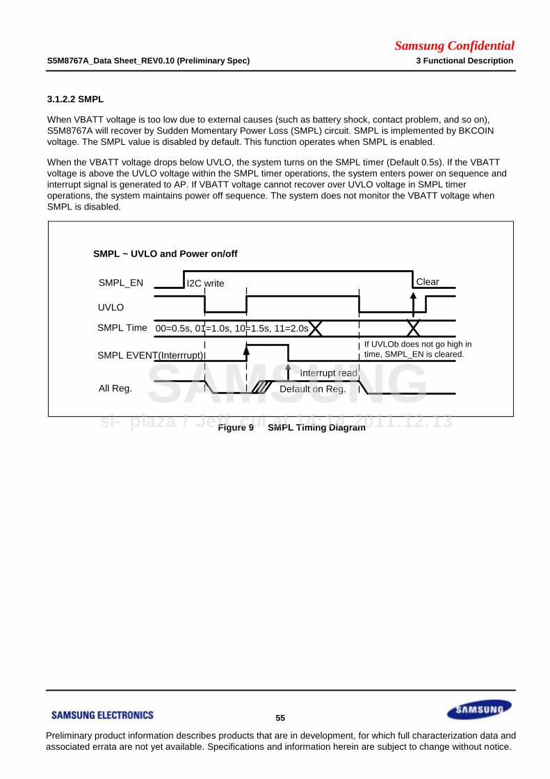
Samsung Confidential S5M8767A_Data Sheet_REV0.10 (Preliminary Spec) 3 Functional Description
55
Preliminary product information describes products that are in development, for which full characterization data and
associated errata are not yet available. Specifications and information herein are subject to change without notice.
3.1.2.2 SMPL
When VBATT voltage is too low due to external causes (such as battery shock, contact problem, and so on),
S5M8767A will recover by Sudden Momentary Power Loss (SMPL) circuit. SMPL is implemented by BKCOIN
voltage. The SMPL value is disabled by default. This function operates when SMPL is enabled.
When the VBATT voltage drops below UVLO, the system turns on the SMPL timer (Default 0.5s). If the VBATT
voltage is above the UVLO voltage within the SMPL timer operations, the system enters power on sequence and
interrupt signal is generated to AP. If VBATT voltage cannot recover over UVLO voltage in SMPL timer
operations, the system maintains power off sequence. The system does not monitor the VBATT voltage when
SMPL is disabled.
All Reg. Default on Reg.
SMPL EVENT(Interrrupt)
SMPL Time
UVLO
SMPL_EN I2C write Clear
00=0.5s, 01=1.0s, 10=1.5s, 11=2.0s
If UVLOb does not go high in
time, SMPL_EN is cleared.
Interrupt read
SMPL ~ UVLO and Power on/off
Figure 9 SMPL Timing Diagram
si-plaza / Jeff_cui at 14:14,2011.12.13
SAMSUNG
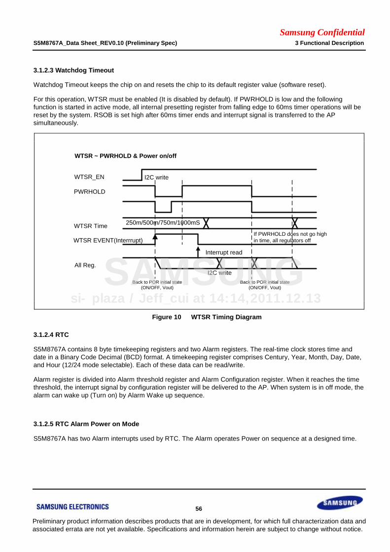
Samsung Confidential S5M8767A_Data Sheet_REV0.10 (Preliminary Spec) 3 Functional Description
56
Preliminary product information describes products that are in development, for which full characterization data and
associated errata are not yet available. Specifications and information herein are subject to change without notice.
3.1.2.3 Watchdog Timeout
Watchdog Timeout keeps the chip on and resets the chip to its default register value (software reset).
For this operation, WTSR must be enabled (It is disabled by default). If PWRHOLD is low and the following
function is started in active mode, all internal presetting register from falling edge to 60ms timer operations will be
reset by the system. RSOB is set high after 60ms timer ends and interrupt signal is transferred to the AP
simultaneously.
All Reg.
Back to POR initial state
(ON/OFF, Vout)
WTSR EVENT(Interrrupt)
WTSR Time
PWRHOLD
WTSR_EN I2C write
250m/500m/750m/1000mS
If PWRHOLD does not go high
in time, all regulators off
Interrupt read
I2C write
WTSR ~ PWRHOLD & Power on/off
Back to POR initial state
(ON/OFF, Vout)
Figure 10 WTSR Timing Diagram
3.1.2.4 RTC
S5M8767A contains 8 byte timekeeping registers and two Alarm registers. The real-time clock stores time and
date in a Binary Code Decimal (BCD) format. A timekeeping register comprises Century, Year, Month, Day, Date,
and Hour (12/24 mode selectable). Each of these data can be read/write.
Alarm register is divided into Alarm threshold register and Alarm Configuration register. When it reaches the time
threshold, the interrupt signal by configuration register will be delivered to the AP. When system is in off mode, the
alarm can wake up (Turn on) by Alarm Wake up sequence.
3.1.2.5 RTC Alarm Power on Mode
S5M8767A has two Alarm interrupts used by RTC. The Alarm operates Power on sequence at a designed time.
si-plaza / Jeff_cui at 14:14,2011.12.13
SAMSUNG
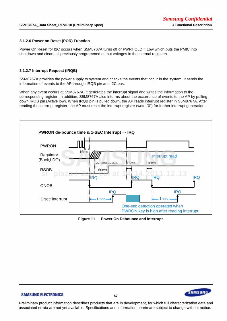
Samsung Confidential S5M8767A_Data Sheet_REV0.10 (Preliminary Spec) 3 Functional Description
57
Preliminary product information describes products that are in development, for which full characterization data and
associated errata are not yet available. Specifications and information herein are subject to change without notice.
3.1.2.6 Power on Reset (POR) Function
Power On Reset for I2C occurs when S5M8767A turns off or PWRHOLD = Low which puts the PMIC into
shutdown and clears all previously programmed output voltages in the internal registers.
3.1.2.7 Interrupt Request (IRQB)
S5M8767A provides the power supply to system and checks the events that occur in the system. It sends the
information of events to the AP through IRQB pin and I2C bus.
When any event occurs at S5M8767A, it generates the interrupt signal and writes the information to the
corresponding register. In addition, S5M8767A also informs about the occurrence of events to the AP by pulling
down IRQB pin (Active low). When IRQB pin is pulled down, the AP reads interrupt register in S5M8767A. After
reading the interrupt register, the AP must reset the interrupt register (write "0") for further interrupt generation.
16ms
16ms 16ms
60ms
IRQ IRQ IRQ IRQ
1-sec 1-sec
IRQ
Interrupt read
One-sec detection operates when
PWRON key is high after reading interrupt
PWRON
Regulator
(Buck,LDO)
RSOB
ONOB
1-sec Interrupt
PWRON de-bounce time & 1-SEC Interrupt → IRQ
after LDO3 goes high
IRQ
Figure 11 Power On Debounce and Interrupt
si-plaza / Jeff_cui at 14:14,2011.12.13
SAMSUNG
Samsung Confidential S5M8767A_Data Sheet_REV0.10 (Preliminary Spec) 3 Functional Description
58
Preliminary product information describes products that are in development, for which full characterization data and
associated errata are not yet available. Specifications and information herein are subject to change without notice.
3.2 UVLO, Reference Voltage, Thermal Shutdown
S5M8767A contains Under-Voltage Lock Out (UVLO). The thermal protection limits total power dissipation.
Reference block supplies voltage reference for regulators and internal block, and it has a noise filter to suppress
voltage fluctuation.
3.2.1.1 Under-Voltage Lock Out (UVLO)
The UVLO circuit for the S5M8767A prevents the device from malfunctioning at low-input voltages and from
excessive discharge of the battery. As VBAT voltage is under UVLO threshold, the S5M8767A enters into UVLO
state which forces the device to a inactive state until the VBAT is high enough to allow the device to operate
normal function.
The UVLO voltage level are 3.1 V rising and 2.55 V falling (hysteresis 550 mV), respectively. In case the VIN
voltage rises over 3.1 V, S5M8767A including all regulators starts to operate from lockout state and if the VBAT
voltage falls under 2.55 V, S5M8767A is turned off.
3.2.1.2 Reference Voltage and Thermal Shutdown
When VBATT is applied, UVLO, Reference Voltage (VREF), and BKCOIN start to work. VREF generates 0.8V
output and no current can be loaded from VREF for external use. Loading any current from this node can drop the
voltage in reference and LDO output. VREF needs an external bypass capacitor (over 100nF) for noise reduction.
Thermal overload protection in each regulator limits total power dissipation in S5M8767A which shut downs
corresponding regulator at a die temperature of 160 C above and turns it on with a down hysteresis of 20 C.
si-plaza / Jeff_cui at 14:14,2011.12.13
SAMSUNG
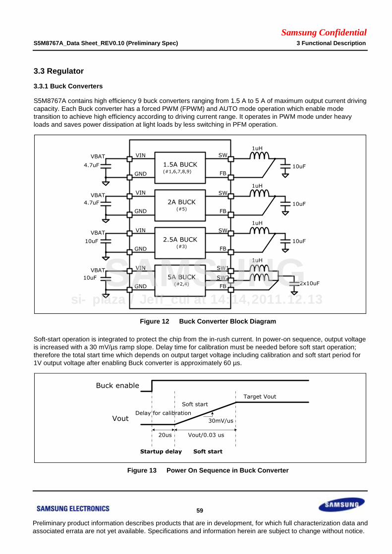
Samsung Confidential S5M8767A_Data Sheet_REV0.10 (Preliminary Spec) 3 Functional Description
59
Preliminary product information describes products that are in development, for which full characterization data and
associated errata are not yet available. Specifications and information herein are subject to change without notice.
3.3 Regulator
3.3.1 Buck Converters
S5M8767A contains high efficiency 9 buck converters ranging from 1.5 A to 5 A of maximum output current driving
capacity. Each Buck converter has a forced PWM (FPWM) and AUTO mode operation which enable mode
transition to achieve high efficiency according to driving current range. It operates in PWM mode under heavy
loads and saves power dissipation at light loads by less switching in PFM operation.
1.5A BUCK(#1,6,7,8,9)
2A BUCK(#5)
2.5A BUCK(#3)
5A BUCK(#2,4)
SW
FB
SW
FB
SW
FB
SW1
FB
SW2
GND
VIN
GND
VIN
GND
VIN
GND
VIN
VBAT
VBAT
VBAT
VBAT
1uH
10uF
1uH
10uF
1uH
10uF
2x10uF
1uH
10uF
10uF
4.7uF
4.7uF
Figure 12 Buck Converter Block Diagram
Soft-start operation is integrated to protect the chip from the in-rush current. In power-on sequence, output voltage
is increased with a 30 mV/µs ramp slope. Delay time for calibration must be needed before soft start operation;
therefore the total start time which depends on output target voltage including calibration and soft start period for
1V output voltage after enabling Buck converter is approximately 60 µs.
Buck enable
Vout
20us
30mV/us
Soft start
Delay for calibration
Target Vout
Vout/0.03 us
Startup delay Soft start
Figure 13 Power On Sequence in Buck Converter
si-plaza / Jeff_cui at 14:14,2011.12.13
SAMSUNG
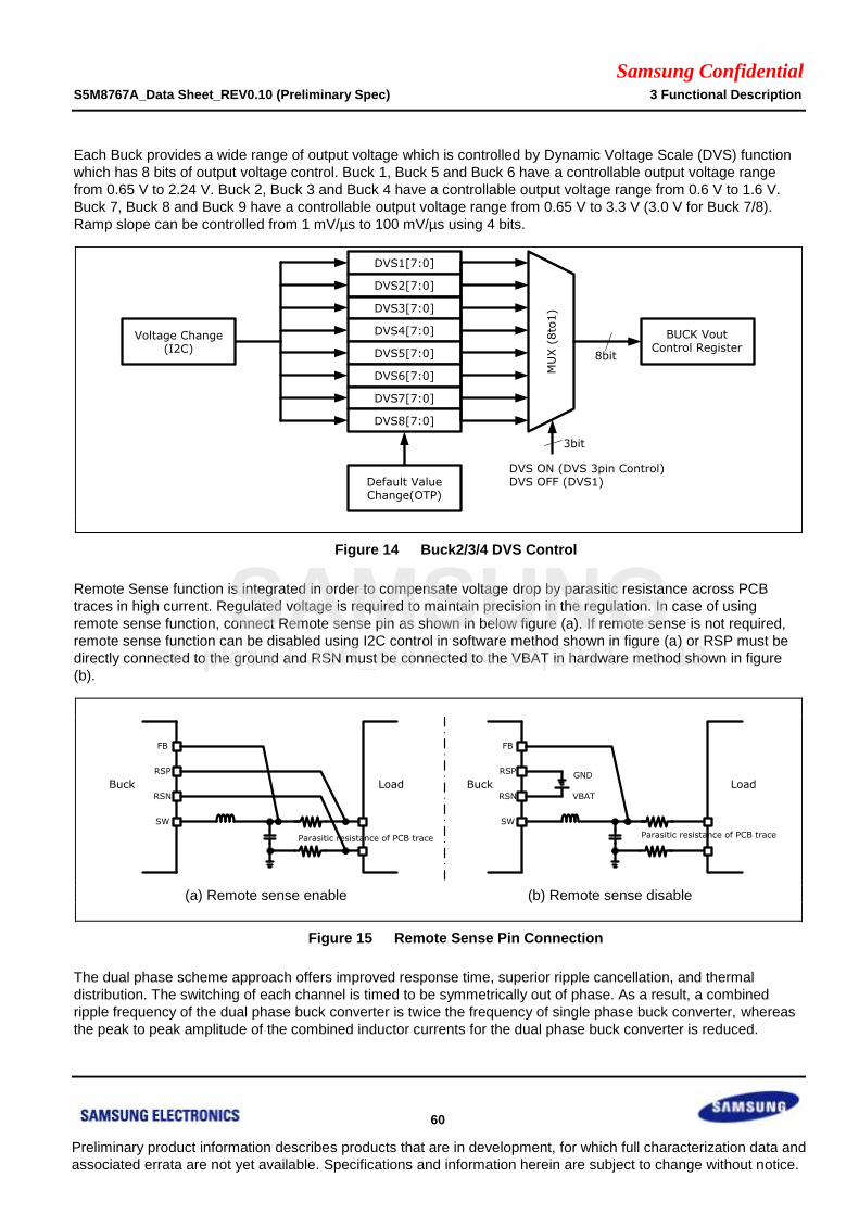
Samsung Confidential S5M8767A_Data Sheet_REV0.10 (Preliminary Spec) 3 Functional Description
60
Preliminary product information describes products that are in development, for which full characterization data and
associated errata are not yet available. Specifications and information herein are subject to change without notice.
Each Buck provides a wide range of output voltage which is controlled by Dynamic Voltage Scale (DVS) function
which has 8 bits of output voltage control. Buck 1, Buck 5 and Buck 6 have a controllable output voltage range
from 0.65 V to 2.24 V. Buck 2, Buck 3 and Buck 4 have a controllable output voltage range from 0.6 V to 1.6 V.
Buck 7, Buck 8 and Buck 9 have a controllable output voltage range from 0.65 V to 3.3 V (3.0 V for Buck 7/8).
Ramp slope can be controlled from 1 mV/µs to 100 mV/µs using 4 bits.
DVS1[7:0]
DVS2[7:0]
DVS3[7:0]
DVS4[7:0]
DVS5[7:0]
DVS6[7:0]
DVS7[7:0]
DVS8[7:0]
Voltage Change (I2C)
Default Value Change(OTP)
MU
X (
8to
1)
BUCK Vout Control Register
DVS ON (DVS 3pin Control)DVS OFF (DVS1)
8bit
3bit
Figure 14 Buck2/3/4 DVS Control
Remote Sense function is integrated in order to compensate voltage drop by parasitic resistance across PCB
traces in high current. Regulated voltage is required to maintain precision in the regulation. In case of using
remote sense function, connect Remote sense pin as shown in below figure (a). If remote sense is not required,
remote sense function can be disabled using I2C control in software method shown in figure (a) or RSP must be
directly connected to the ground and RSN must be connected to the VBAT in hardware method shown in figure
(b).
Buck Load
FB
RSP
RSN
SW
Load
FB
RSP
RSN
SW
GND
VBAT
Parasitic resistance of PCB trace Parasitic resistance of PCB trace
Buck
(a) Remote sense enable (b) Remote sense disable
Figure 15 Remote Sense Pin Connection
The dual phase scheme approach offers improved response time, superior ripple cancellation, and thermal
distribution. The switching of each channel is timed to be symmetrically out of phase. As a result, a combined
ripple frequency of the dual phase buck converter is twice the frequency of single phase buck converter, whereas
the peak to peak amplitude of the combined inductor currents for the dual phase buck converter is reduced.
si-plaza / Jeff_cui at 14:14,2011.12.13
SAMSUNG
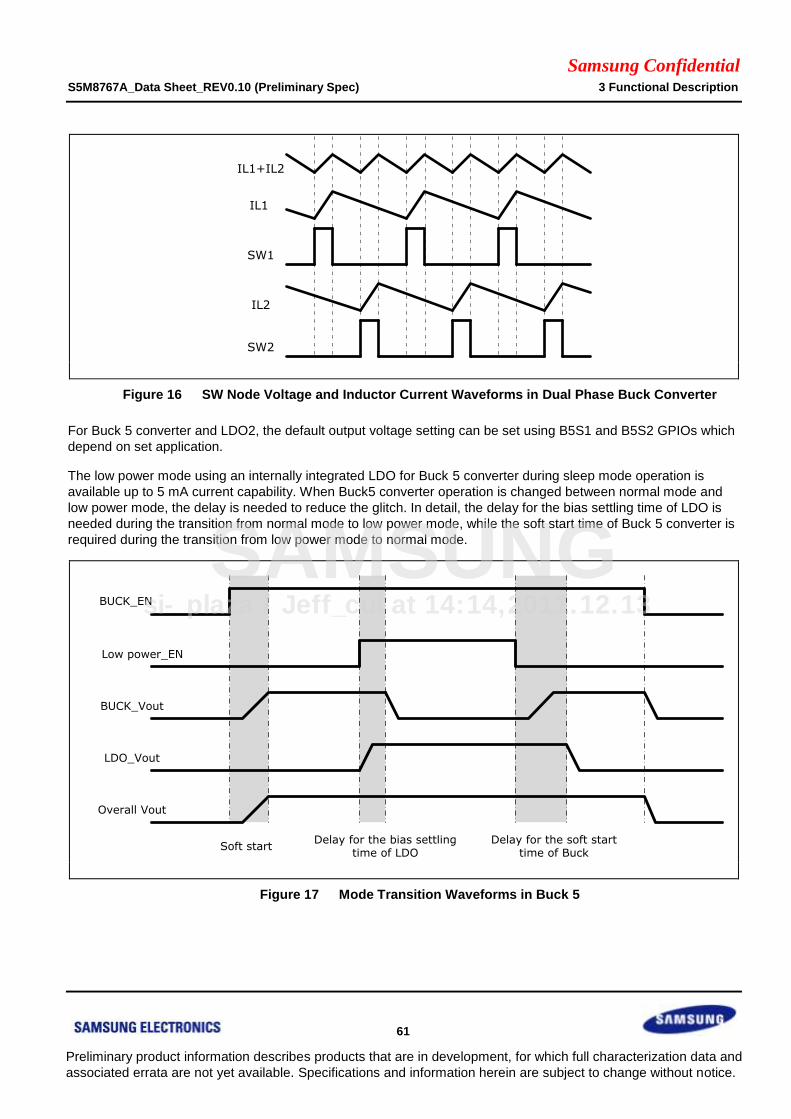
Samsung Confidential S5M8767A_Data Sheet_REV0.10 (Preliminary Spec) 3 Functional Description
61
Preliminary product information describes products that are in development, for which full characterization data and
associated errata are not yet available. Specifications and information herein are subject to change without notice.
SW1
SW2
IL2
IL1
IL1+IL2
Figure 16 SW Node Voltage and Inductor Current Waveforms in Dual Phase Buck Converter
For Buck 5 converter and LDO2, the default output voltage setting can be set using B5S1 and B5S2 GPIOs which
depend on set application.
The low power mode using an internally integrated LDO for Buck 5 converter during sleep mode operation is
available up to 5 mA current capability. When Buck5 converter operation is changed between normal mode and
low power mode, the delay is needed to reduce the glitch. In detail, the delay for the bias settling time of LDO is
needed during the transition from normal mode to low power mode, while the soft start time of Buck 5 converter is
required during the transition from low power mode to normal mode.
BUCK_EN
Low power_EN
BUCK_Vout
LDO_Vout
Overall Vout
Soft startDelay for the bias settling
time of LDODelay for the soft start
time of Buck
Figure 17 Mode Transition Waveforms in Buck 5
si-plaza / Jeff_cui at 14:14,2011.12.13
SAMSUNG

Samsung Confidential S5M8767A_Data Sheet_REV0.10 (Preliminary Spec) 3 Functional Description
62
Preliminary product information describes products that are in development, for which full characterization data and
associated errata are not yet available. Specifications and information herein are subject to change without notice.
3.3.1.1 Inductor Selection
The inductor can be chosen with two main considerations which include its DC resistance (DCR) and saturation
current. Since the inductor value has a significant impact on the ripple current and output voltage ripple, it should
be carefully considered. A 1.0 H inductor with a saturation current of at least 2 A to 2.5 A is strongly
recommended for high load capacity buck converters (Buck2/3/4/5) with a full load. For medium load capacity
buck converters (Buck1/6/7/8/9), a slightly smaller size is allowed. Also, inductor rated current can be reduced
with lower DCR. For maximum efficiency, the inductor’s DCR should be as low as possible.
NOTE: The inductor type and core materials are different among several manufacturers and affect the converter efficiency.
See Table 1 for suggested inductors and their manufacturers. You may choose other manufacturers’ inductors with
similar inductor value and DCR.
Table 1 List of Recommended Inductors
Model Number Inductor Value
(H) Vendor
Dimension
L W H (mm)
Max. IDC
(A)
Max. DCR
(m)
1.0 H Multi-Layer Chip or Metal Alloy Type Power Inductor for Buck2/3/4/5 (High Load Capacity)
DFE252010C 1.0 TOKO 2.5 x 2.0 x 1.0 3.0 60
CIG22H1R0MAE 1.0 SEM 2.5 x 2.0 x 0.9 2.3 65
TFM252010A-1R0M 1.0 TDK 2.5 x 2.0 x 1.0 2.5 65
LQM2HPN1R0NGHL07 1.0 Murata 2.5 x 2.0 x 0.9 2 100
DFE252012C 1.0 TOKO 2.5 x 2.0 x 1.2 3.8 59
1.0 H Multi-Layer Chip Type or Metal Alloy Power Inductor for Buck1/6/7/8/9 (Medium Load Capacity)
DFE201610C 1.0 TOKO 2.0 x 1.6 x 1.0 2.0 80
MDT2012-CR1R0N 1.0 TOKO 2.0 x 1.2 x 1.0 2.15 80
CIG21L1R0MNE 1.0 SEM 2.0 x 1.2 x 1.0 1.15 110
MLP2012L1R0M 1.0 TDK 2.0 x 1.2 x 1.0 1.2 100
LQM2MPN1R0MG0 1.0 Murata 2.0 x 1.6 x 1.0 1.4 55
3.3.1.2 Capacitor Selection
Ceramic capacitors are used for most linear regulators’ and switching converters’ input and output filters. Low
equivalent series resistance (ESR) ceramic capacitors should be chosen as output filter capacitors and input filter
capacitors. Since X5R or X7R ceramic capacitors maintain their capacitance over a wide voltage range and
temperature range, X5R or X7R ceramic capacitors are strongly recommended.
3.3.1.3 Output Capacitors
The output ripple voltage depends upon the charging and discharging of output capacitor and depends upon the
ESR too. A X5R or X7R type of 10 F ceramic output capacitor with low ESR is recommended for linear
regulators and switching converters. This keeps the output ripple voltage small and ensures good transient
response for converter with loop stability over a wide operating temperature range and voltage.
si-plaza / Jeff_cui at 14:14,2011.12.13
SAMSUNG
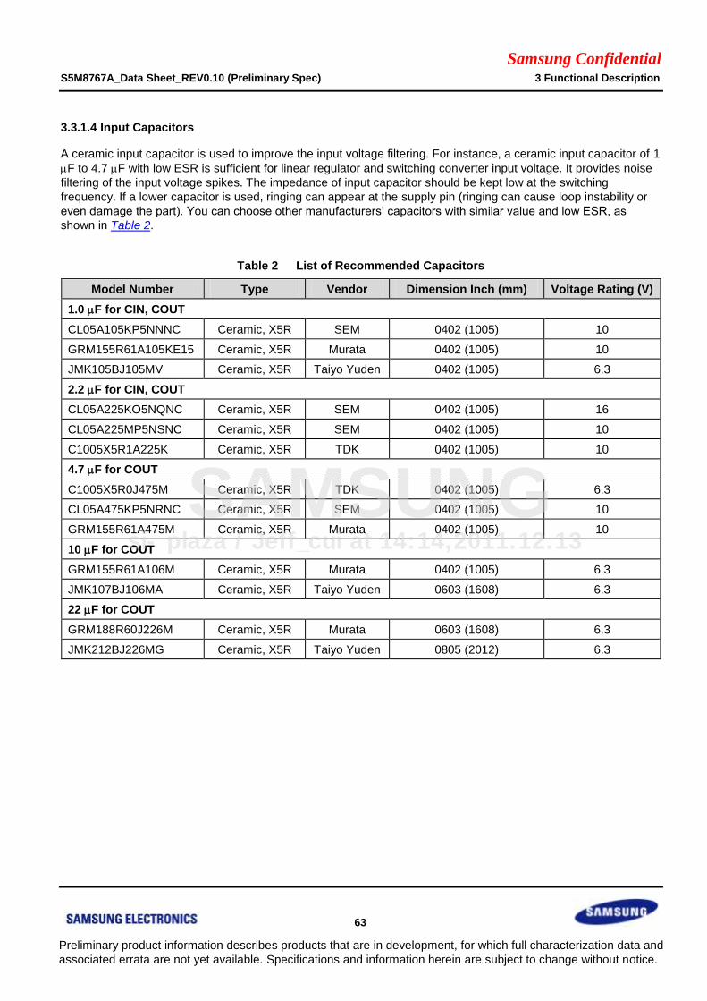
Samsung Confidential S5M8767A_Data Sheet_REV0.10 (Preliminary Spec) 3 Functional Description
63
Preliminary product information describes products that are in development, for which full characterization data and
associated errata are not yet available. Specifications and information herein are subject to change without notice.
3.3.1.4 Input Capacitors
A ceramic input capacitor is used to improve the input voltage filtering. For instance, a ceramic input capacitor of 1
F to 4.7 F with low ESR is sufficient for linear regulator and switching converter input voltage. It provides noise
filtering of the input voltage spikes. The impedance of input capacitor should be kept low at the switching
frequency. If a lower capacitor is used, ringing can appear at the supply pin (ringing can cause loop instability or
even damage the part). You can choose other manufacturers’ capacitors with similar value and low ESR, as
shown in Table 2.
Table 2 List of Recommended Capacitors
Model Number Type Vendor Dimension Inch (mm) Voltage Rating (V)
1.0 F for CIN, COUT
CL05A105KP5NNNC Ceramic, X5R SEM 0402 (1005) 10
GRM155R61A105KE15 Ceramic, X5R Murata 0402 (1005) 10
JMK105BJ105MV Ceramic, X5R Taiyo Yuden 0402 (1005) 6.3
2.2 F for CIN, COUT
CL05A225KO5NQNC Ceramic, X5R SEM 0402 (1005) 16
CL05A225MP5NSNC Ceramic, X5R SEM 0402 (1005) 10
C1005X5R1A225K Ceramic, X5R TDK 0402 (1005) 10
4.7 F for COUT
C1005X5R0J475M Ceramic, X5R TDK 0402 (1005) 6.3
CL05A475KP5NRNC Ceramic, X5R SEM 0402 (1005) 10
GRM155R61A475M Ceramic, X5R Murata 0402 (1005) 10
10 F for COUT
GRM155R61A106M Ceramic, X5R Murata 0402 (1005) 6.3
JMK107BJ106MA Ceramic, X5R Taiyo Yuden 0603 (1608) 6.3
22 F for COUT
GRM188R60J226M Ceramic, X5R Murata 0603 (1608) 6.3
JMK212BJ226MG Ceramic, X5R Taiyo Yuden 0805 (2012) 6.3
si-plaza / Jeff_cui at 14:14,2011.12.13
SAMSUNG
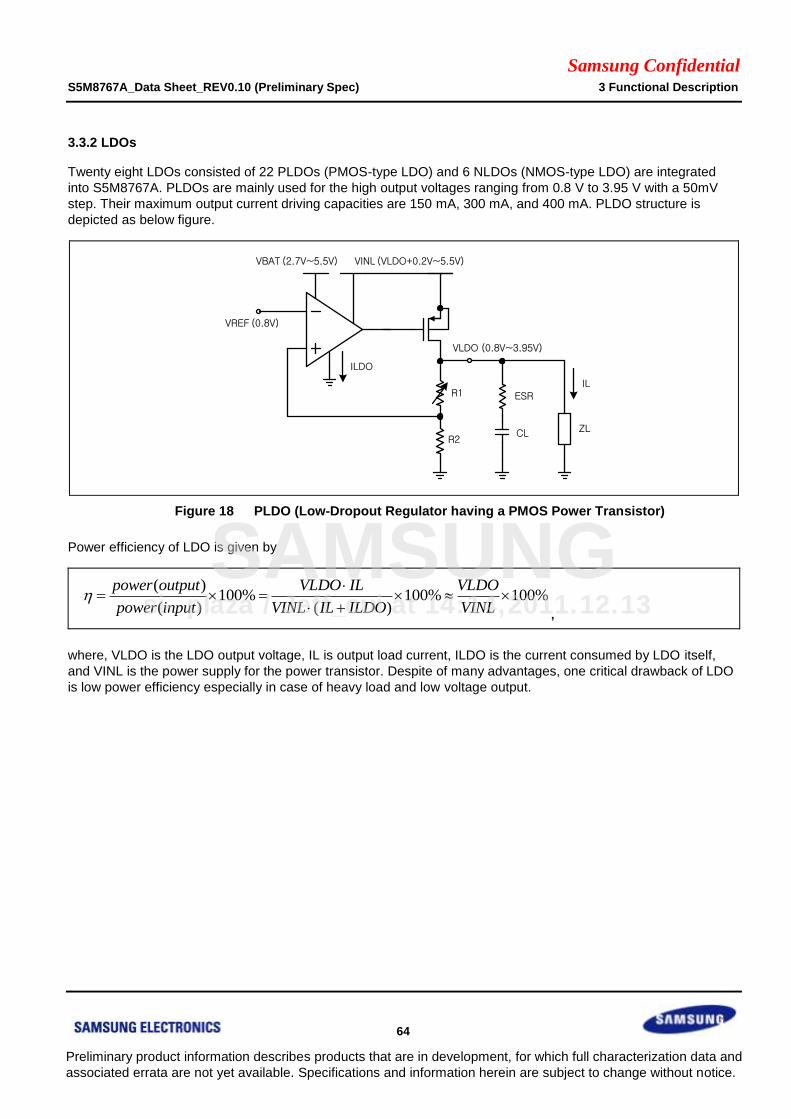
Samsung Confidential S5M8767A_Data Sheet_REV0.10 (Preliminary Spec) 3 Functional Description
64
Preliminary product information describes products that are in development, for which full characterization data and
associated errata are not yet available. Specifications and information herein are subject to change without notice.
3.3.2 LDOs
Twenty eight LDOs consisted of 22 PLDOs (PMOS-type LDO) and 6 NLDOs (NMOS-type LDO) are integrated
into S5M8767A. PLDOs are mainly used for the high output voltages ranging from 0.8 V to 3.95 V with a 50mV
step. Their maximum output current driving capacities are 150 mA, 300 mA, and 400 mA. PLDO structure is
depicted as below figure.
VINL (VLDO+0.2V~5.5V)
VLDO (0.8V~3.95V)
VREF (0.8V)
R1
R2
ESR
CL ZL
IL
VBAT (2.7V~5.5V)
ILDO
Figure 18 PLDO (Low-Dropout Regulator having a PMOS Power Transistor)
Power efficiency of LDO is given by
( )100% 100% 100%
( ) ( )
power output VLDO IL VLDO
power input VINL IL ILDO VINL
,
where, VLDO is the LDO output voltage, IL is output load current, ILDO is the current consumed by LDO itself,
and VINL is the power supply for the power transistor. Despite of many advantages, one critical drawback of LDO
is low power efficiency especially in case of heavy load and low voltage output.
si-plaza / Jeff_cui at 14:14,2011.12.13
SAMSUNG
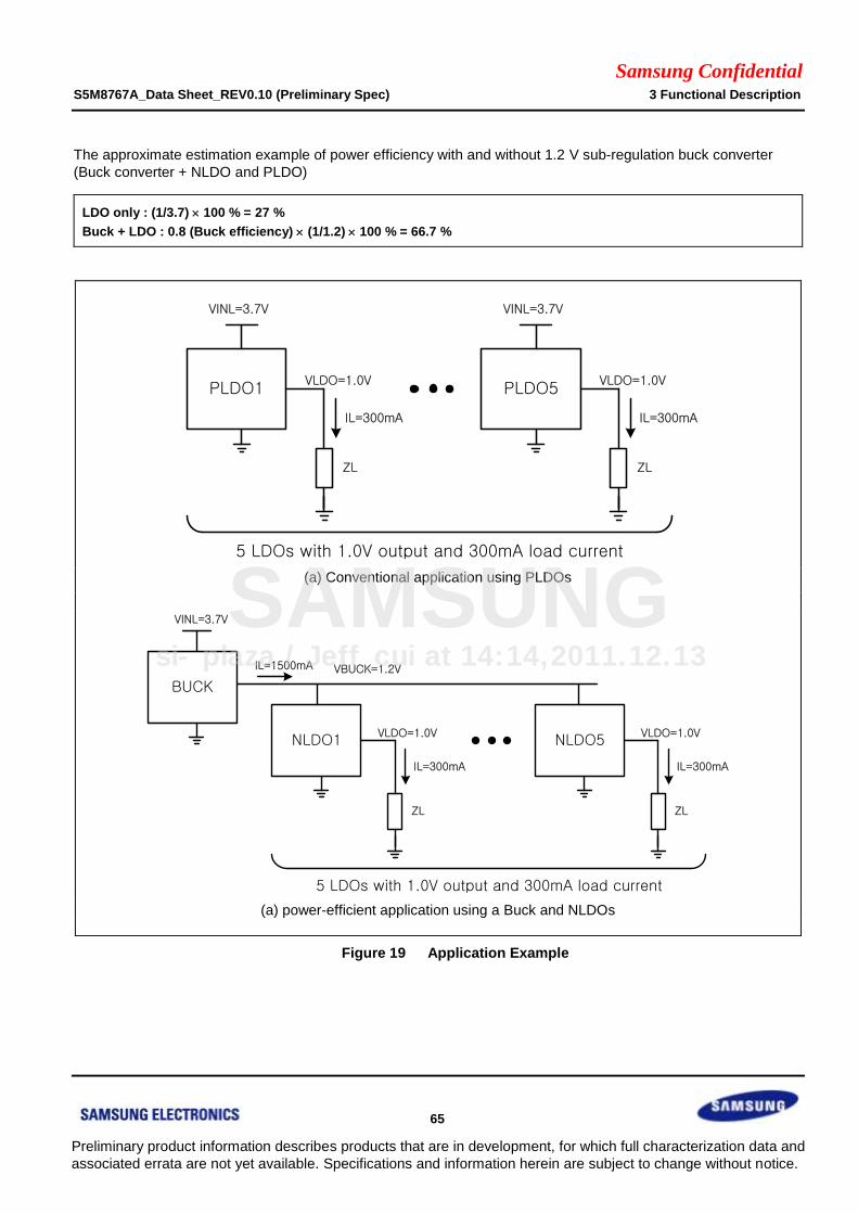
Samsung Confidential S5M8767A_Data Sheet_REV0.10 (Preliminary Spec) 3 Functional Description
65
Preliminary product information describes products that are in development, for which full characterization data and
associated errata are not yet available. Specifications and information herein are subject to change without notice.
The approximate estimation example of power efficiency with and without 1.2 V sub-regulation buck converter
(Buck converter + NLDO and PLDO)
LDO only : (1/3.7) 100 % = 27 %
Buck + LDO : 0.8 (Buck efficiency) (1/1.2) 100 % = 66.7 %
PLDO1VLDO=1.0V
ZL
IL=300mA
VINL=3.7V
PLDO5VLDO=1.0V
ZL
IL=300mA
VINL=3.7V
5 LDOs with 1.0V output and 300mA load current
(a) Conventional application using PLDOs
NLDO1VLDO=1.0V
ZL
IL=300mA
VINL=3.7V
NLDO5VLDO=1.0V
ZL
IL=300mA
5 LDOs with 1.0V output and 300mA load current
BUCK
IL=1500mA VBUCK=1.2V
(a) power-efficient application using a Buck and NLDOs
Figure 19 Application Example
si-plaza / Jeff_cui at 14:14,2011.12.13
SAMSUNG
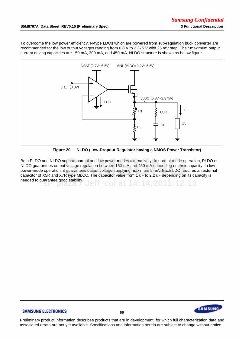
Samsung Confidential S5M8767A_Data Sheet_REV0.10 (Preliminary Spec) 3 Functional Description
66
Preliminary product information describes products that are in development, for which full characterization data and
associated errata are not yet available. Specifications and information herein are subject to change without notice.
To overcome the low power efficiency, N-type LDOs which are powered from sub-regulation buck converter are
recommended for the low output voltages ranging from 0.8 V to 2.375 V with 25 mV step. Their maximum output
current driving capacities are 150 mA, 300 mA, and 450 mA. NLDO structure is shown as below figure.
VBAT (2.7V~5.5V) VINL (VLDO+0.2V~5.5V)
VLDO (0.8V~2.375V)
VREF (0.8V)
R1
R2
ESR
CL ZL
IL
ILDO
Figure 20 NLDO (Low-Dropout Regulator having a NMOS Power Transistor)
Both PLDO and NLDO support normal and low power modes alternatively. In normal-mode operation, PLDO or
NLDO guarantees output voltage regulation between 150 mA and 450 mA depending on their capacity. In low-
power-mode operation, it guarantees output voltage supplying maximum 5 mA. Each LDO requires an external
capacitor of X5R and X7R type MLCC. The capacitor value from 1 uF to 2.2 uF depending on its capacity is
needed to guarantee good stability.
si-plaza / Jeff_cui at 14:14,2011.12.13
SAMSUNG
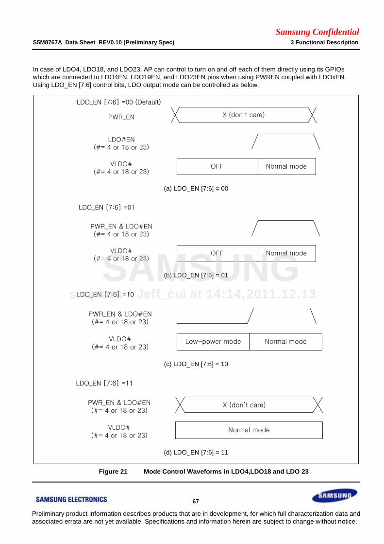
Samsung Confidential S5M8767A_Data Sheet_REV0.10 (Preliminary Spec) 3 Functional Description
67
Preliminary product information describes products that are in development, for which full characterization data and
associated errata are not yet available. Specifications and information herein are subject to change without notice.
In case of LDO4, LDO18, and LDO23, AP can control to turn on and off each of them directly using its GPIOs
which are connected to LDO4EN, LDO19EN, and LDO23EN pins when using PWREN coupled with LDOxEN.
Using LDO_EN [7:6] control bits, LDO output mode can be controlled as below.
LDO_EN [7:6] =00 (Default)
LDO#EN(#= 4 or 18 or 23)
VLDO# (#= 4 or 18 or 23)
Normal modeOFF
PWR_EN X (don’t care)
(a) LDO_EN [7:6] = 00
LDO_EN [7:6] =01
PWR_EN & LDO#EN(#= 4 or 18 or 23)
VLDO# (#= 4 or 18 or 23)
Normal modeOFF
(b) LDO_EN [7:6] = 01
LDO_EN [7:6] =10
PWR_EN & LDO#EN(#= 4 or 18 or 23)
VLDO# (#= 4 or 18 or 23)
Normal modeLow-power mode
(c) LDO_EN [7:6] = 10
LDO_EN [7:6] =11
PWR_EN & LDO#EN(#= 4 or 18 or 23)
VLDO# (#= 4 or 18 or 23)
Normal mode
X (don’t care)
(d) LDO_EN [7:6] = 11
Figure 21 Mode Control Waveforms in LDO4,LDO18 and LDO 23
si-plaza / Jeff_cui at 14:14,2011.12.13
SAMSUNG

Samsung Confidential S5M8767A_Data Sheet_REV0.10 (Preliminary Spec) 3 Functional Description
68
Preliminary product information describes products that are in development, for which full characterization data and
associated errata are not yet available. Specifications and information herein are subject to change without notice.
Table 3 Information of Power Supply on Each LDO
LDO Default Voltage Max. Current Voltage Range/Step (I2C) Purpose_AP, Peri (NOTE)
LDO1 1.0 V 150 mA 0.8 V to 2.375 V, 25 mV step
Alive
LDO2 1.2 V 450 mA VDDQ_M1/M2
LDO3 1.8 V 300 mA
0.8 V to 3.95 V, 50 mV Step
E, SBUS, GPIO, MIPIHSI,
RTC, CKO, SYS33
LDO4 1.8 V 150 mA VDD_PRE
LDO5 1.8 V 150 mA VCC_18_IO
LDO6 1.0 V 150 mA
0.8 V to 2.375 V, 25 mV step
VDD10_MPLL
LDO7 1.0 V 150 mA VDD10_VPLL ,EPLL,APLL
LDO8 1.0 V 300 mA VDD10_HDMI, HDMI_PLL,
MIPI, MIPI_PLL, MIPI2L
LDO9 3.0 V 400 mA
0.8 V to 3.95 V, 50 mV Step
VDD33_EFNAND
LDO10 1.8 V 300 mA VDD18_ HDMI_OSC , MIPI,
MIPI2L,ADC,TS
LDO11 1.8 V 150 mA VDD18_ABB1
LDO12 3.0 V 150 mA VDD33_UOTG
LDO13 1.8 V 150 mA VDDQ_C2C
LDO14 1.8 V 150 mA VDD18_ABB0, ABB2
LDO15 1.0 V 150 mA 0.8 V to 2.375 V, 25 mV step VDD10_HSIC, UOTG
LDO16 1.8 V 150 mA
0.8 V to 3.95 V, 50 mV Step
VDD18_HSIC
LDO17 2.8 V 150 mA VDDQ_MMC01/MMC2
LDO18 2.8 V 300 mA VDDF_eMMC
LDO19 3.0 V 150 mA Cam_AF
LDO20 3.0 V 150 mA VCC-LCD
LDO21 3.0 V 150 mA Haptic Motor Driver
LDO22 3.3 V 150 mA IRDA (LEDA)
LDO23 2.8 V 300 mA T-Flash
LDO24 3.0 V 300 mA Touch
LDO25 1.2 V 300 mA Cam Sensor
LDO26 1.8 V 150 mA CAM ISP
LDO27 1.8 V 150 mA VT Cam
LDO28 1.8 V 150 mA CAM_ISP_MIPI
NOTE: Samsung Application Processor is recommended.
si-plaza / Jeff_cui at 14:14,2011.12.13
SAMSUNG

Samsung Confidential S5M8767A_Data Sheet_REV0.10 (Preliminary Spec) 3 Functional Description
69
Preliminary product information describes products that are in development, for which full characterization data and
associated errata are not yet available. Specifications and information herein are subject to change without notice.
3.4 Backup Coin Battery
3.4.1 Backup Coin Battery
The backup coin battery charger is a voltage limited current source with a 1 k output resistor. This charger is
always on regardless of power on/off status (except if the main battery voltage is below UVLO). Backup Charger
has an I2C controlled output voltage from 2.5 V to 3.5 V with a default output voltage of 3.0 V. This charger can
also support a super capacitor.
IBKBATT
100uA
VBKBATTBackup Coin Charger
CC mode
Coin Charger
CV mode
Figure 22 Backup Coin Battery Charging Graph
si-plaza / Jeff_cui at 14:14,2011.12.13
SAMSUNG
Samsung Confidential S5M8767A_Data Sheet_REV0.10 (Preliminary Spec) 4 Digital Interface (I2C)
70
Preliminary product information describes products that are in development, for which full characterization data and
associated errata are not yet available. Specifications and information herein are subject to change without notice.
4 Digital Interface (I2C)
S5M8767A is controlled through the I2C interface. The operational mode in S5M8767A is set by the I2C. Read
and Write modes are also supported. S5M8767A is activated only as a slave mode.
Access Mode Host (Master) S5M8767A (Slave)
Write Transmitter Receiver
Read Receiver Transmitter
4.1 Slave Address
Slave address is used to select the S5M8767A on the I2C bus. This address consists of 8-bit data. The LSB 1-bit
determines the read or write mode. If the LSB 1-bit is low, the write mode is selected.
Section Address selection Access Mode
PM section 1100 1100 (0CC) PM Write
1100 1101 (0CD) PM Read
RTC section 0000 1100 (00C) RTC Write
0000 1101 (00D) RTC Read
si-plaza / Jeff_cui at 14:14,2011.12.13
SAMSUNG
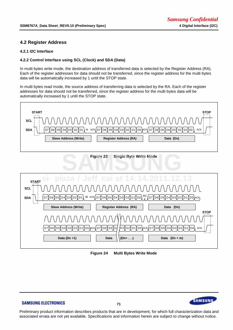
Samsung Confidential S5M8767A_Data Sheet_REV0.10 (Preliminary Spec) 4 Digital Interface (I2C)
71
Preliminary product information describes products that are in development, for which full characterization data and
associated errata are not yet available. Specifications and information herein are subject to change without notice.
4.2 Register Address
4.2.1 I2C Interface
4.2.2 Control Interface using SCL (Clock) and SDA (Data)
In multi bytes write mode, the destination address of transferred data is selected by the Register Address (RA).
Each of the register addresses for data should not be transferred, since the register address for the multi bytes
data will be automatically increased by 1 until the STOP state.
In multi bytes read mode, the source address of transferring data is selected by the RA. Each of the register
addresses for data should not be transferred, since the register address for the multi bytes data will be
automatically increased by 1 until the STOP state.
Figure 23 Single Byte Write Mode
Figure 24 Multi Bytes Write Mode
D7
START
SCL
SDA D6 D5 D4 D3 D2 D1 W ACK D7 D6 D5 D4 D3 D2 D1 D0 ACK D7 D6 D5 D4 D3 D2 D1 D0
STOP
ACK
Slave Address (Write) Register Address (RA) Data (Dn)
Data (Dn+ . . .)
D7
START
SCL
SDA D6 D5 D4 D3 D2 D1 W ACK D7 D6 D5 D4 D3 D2 D1 D0AC
KD7 D6 D5 D4 D3 D2 D1 D0 ACK
D7
STOP
D6 D5 D4 D3 D2 D1 D0 ACK D7 D6 D5 D4 D3 D2 D1 D0 D7 D6 D5 D4 D3 D2 D1 D0 ACKACK
Slave Address (Write) Register Address (RA) Data (Dn)
Data (Dn +1) Data (Dn + m)
si-plaza / Jeff_cui at 14:14,2011.12.13
SAMSUNG
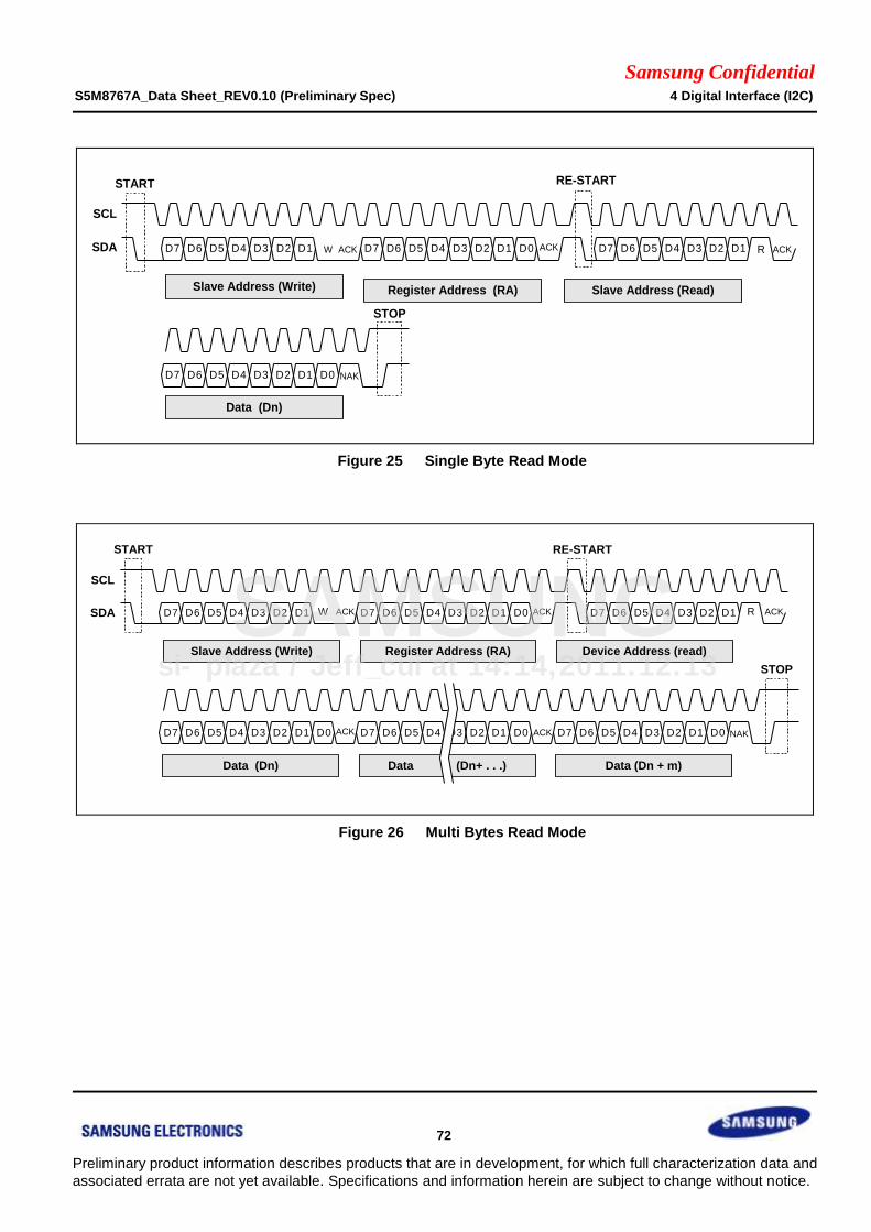
Samsung Confidential S5M8767A_Data Sheet_REV0.10 (Preliminary Spec) 4 Digital Interface (I2C)
72
Preliminary product information describes products that are in development, for which full characterization data and
associated errata are not yet available. Specifications and information herein are subject to change without notice.
Figure 25 Single Byte Read Mode
Figure 26 Multi Bytes Read Mode
D7
START
SCL
SDA D6 D5 D4 D3 D2 D1 D7 D6 D5 D4 D3 D2 D1 D0 D6 D5 D4 D3 D2 D1 R
D7 D6 D5 D4 D3 D2 D1 D0
D7
RE-START
W ACK ACK ACK
STOP
NAK
Slave Address (Write) Register Address (RA) Slave Address (Read)
Data (Dn)
Data (Dn+ . . .)
D7
START
SCL
SDA D6 D5 D4 D3 D2 D1 D7 D6 D5 D4 D3 D2 D1 D0 D6 D5 D4 D3 D2 D1 R
D7 D6 D5 D4 D3 D2 D1 D0 D7 D6 D5 D4 D3 D2 D1 D0 D7 D6 D5 D4 D3 D2 D1 D0
D7
RE-START
W ACK ACK ACK
ACK ACK NAK
STOP
Slave Address (Write) Register Address (RA) Device Address (read)
Data (Dn) Data (Dn + m)
si-plaza / Jeff_cui at 14:14,2011.12.13
SAMSUNG
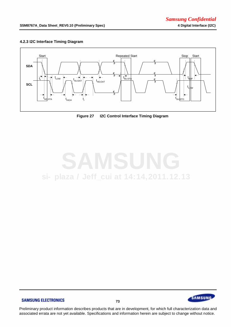
Samsung Confidential S5M8767A_Data Sheet_REV0.10 (Preliminary Spec) 4 Digital Interface (I2C)
73
Preliminary product information describes products that are in development, for which full characterization data and
associated errata are not yet available. Specifications and information herein are subject to change without notice.
4.2.3 I2C Interface Timing Diagram
Figure 27 I2C Control Interface Timing Diagram
Start
tf
tLOW
tHD;STA t
HIGH
tSU;DAT
tSU;STA
tHD;DAT
tr
tBUF
tLOW
tSU;STO
Repeated Start Stop Start
SDA
SCL
si-plaza / Jeff_cui at 14:14,2011.12.13
SAMSUNG
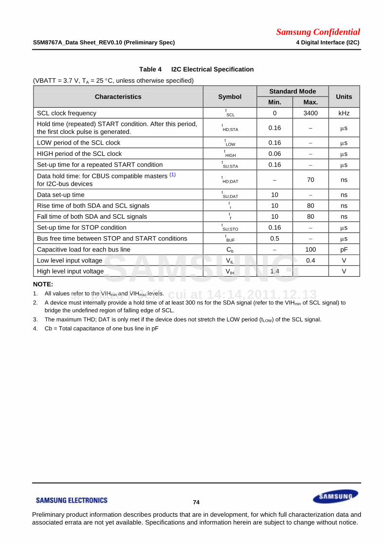
Samsung Confidential S5M8767A_Data Sheet_REV0.10 (Preliminary Spec) 4 Digital Interface (I2C)
74
Preliminary product information describes products that are in development, for which full characterization data and
associated errata are not yet available. Specifications and information herein are subject to change without notice.
Table 4 I2C Electrical Specification
(VBATT = 3.7 V, TA = 25 C, unless otherwise specified)
Characteristics Symbol Standard Mode
Units Min. Max.
SCL clock frequency fSCL 0 3400 kHz
Hold time (repeated) START condition. After this period,
the first clock pulse is generated. tHD;STA 0.16 s
LOW period of the SCL clock tLOW 0.16 s
HIGH period of the SCL clock tHIGH 0.06 s
Set-up time for a repeated START condition tSU;STA 0.16 s
Data hold time: for CBUS compatible masters (1)
for I2C-bus devices tHD;DAT 70 ns
Data set-up time tSU;DAT 10 ns
Rise time of both SDA and SCL signals tr 10 80 ns
Fall time of both SDA and SCL signals tf 10 80 ns
Set-up time for STOP condition tSU;STO 0.16 s
Bus free time between STOP and START conditions tBUF 0.5 s
Capacitive load for each bus line Cb 100 pF
Low level input voltage VIL 0.4 V
High level input voltage VIH 1.4 V
NOTE:
1. All values refer to the VIHmin and VIHmax levels.
2. A device must internally provide a hold time of at least 300 ns for the SDA signal (refer to the VIHmin of SCL signal) to
bridge the undefined region of falling edge of SCL.
3. The maximum THD; DAT is only met if the device does not stretch the LOW period (tLOW) of the SCL signal.
4. Cb = Total capacitance of one bus line in pF
si-plaza / Jeff_cui at 14:14,2011.12.13
SAMSUNG

Samsung Confidential S5M8767A_Data Sheet_REV0.10 (Preliminary Spec) 5 Register Description
75
Preliminary product information describes products that are in development, for which full characterization data and
associated errata are not yet available. Specifications and information herein are subject to change without notice.
5 Register Description
5.1 Power Management
5.1.1 Register Map Summary
Register Address Description Reset Value
PMIC_ID 0x00 PMIC ID Register 0x00
ONOFF INT1 0x01 On/OFF Interrupt 1 Register 0x00
ONOFF INT2 0x02 On/OFF Interrupt 2 Register 0x00
RTC INT3 0x03 RTC Interrupt Register 0x00
ONOFF INT1M 0x04 On/OFF Interrupt 1 Mask Register 0x00
ONOFF INT2M 0x05 On/OFF Interrupt 2 Mask Register 0x78
RTC INT3M 0x06 RTC Interrupt Mask Register 0x00
STATUS1 0x07 Status1 Register N/A
STATUS2 0x08 Status 2 Register N/A
RSVD 0X09 Reserved N/A
CTRL1 0x0A Control 1 Register 0x01
CTRL2 0x0B Control 2 Register 0x0E
RSVD 0x0C Reserved N/A
RSVD 0x0D Reserved N/A
BU_CHG 0x0E Back-Up Charger Register 0x4F
DVS_RAMP 0x0F DVS Ramp Register 0x90
RSVD 0x10 Reserved N/A
RSVD 0x11 Reserved N/A
RSVD 0x12 Reserved N/A
LDO1 0x13 LDO1 Configuration Register 0x22
LDO2 0x14 LDO2 Configuration Register 0x22
LDO3 0x15 LDO3 Configuration Register 0x22
LDO4 0x16 LDO4 Configuration Register 0x22
LDO5 0x17 LDO5 Configuration Register 0x22
LDO6 0x18 LDO6 Configuration Register 0x22
LDO7 0x19 LDO7 Configuration Register 0x22
LDO8 0x1A LDO8 Configuration Register 0x22
LDO9 0x1B LDO9 Configuration Register 0x22
si-plaza / Jeff_cui at 14:14,2011.12.13
SAMSUNG

Samsung Confidential S5M8767A_Data Sheet_REV0.10 (Preliminary Spec) 5 Register Description
76
Preliminary product information describes products that are in development, for which full characterization data and
associated errata are not yet available. Specifications and information herein are subject to change without notice.
Register Address Description Reset Value
LDO10 0x1C LDO10 Configuration Register 0x22
LDO11 0x1D LDO11 Configuration Register 0x22
LDO12 0x1E LDO12 Configuration Register 0x22
LDO13 0x1F LDO13 Configuration Register 0x22
LDO14 0x20 LDO14 Configuration Register 0x22
LDO15 0x21 LDO15 Configuration Register 0x22
LDO16 0x22 LDO16 Configuration Register 0x22
LDO17 0x23 LDO17 Configuration Register 0x22
LDO18 0x24 LDO18 Configuration Register 0x22
LDO19 0x25 LDO19 Configuration Register 0x22
LDO20 0x26 LDO20 Configuration Register 0x22
LDO21 0x27 LDO21 Configuration Register 0x22
LDO22 0x28 LDO22 Configuration Register 0x22
LDO23 0x29 LDO23 Configuration Register 0x22
LDO24 0x2A LDO24 Configuration Register 0x22
LDO25 0x2B LDO25 Configuration Register 0x22
LDO26 0x2C LDO26 Configuration Register 0x22
LDO27 0x2D LDO27 Configuration Register 0x22
LDO28 0x2E LDO28 Configuration Register 0x22
RSVD 0x2F Reserved 0x00
RSVD 0x30 Reserved 0x00
UVLO 0x31 Under Voltage Lock Out Register 0x04
BUCK1_CTRL1 0x32 BUCK1 Control1 Register 0xD8
BUCK1_CTRL2 0x33 BUCK1 Control2 Register 0x38
BUCK2_CTRL 0x34 BUCK2 Control Register 0xFA
BUCK2_DVS1 0x35 BUCK2 DVS1 Register 0x50
BUCK2_DVS2 0x36 BUCK2 DVS2 Register 0x50
BUCK2_DVS3 0x37 BUCK2 DVS3 Register 0x50
BUCK2_DVS4 0x38 BUCK2 DVS4 Register 0x50
BUCK2_DVS5 0x39 BUCK2 DVS5 Register 0x50
BUCK2_DVS6 0x3A BUCK2 DVS6 Register 0x50
BUCK2_DVS7 0x3B BUCK2 DVS7 Register 0x50
BUCK2_DVS8 0x3C BUCK2 DVS8 Register 0x50
BUCK3_CTRL 0x3D BUCK3 Control Register 0xFA
BUCK3_DVS1 0x3E BUCK3 DVS1 Register 0x40
BUCK3_DVS2 0x3F BUCK3 DVS2 Register 0x40
BUCK3_DVS3 0x40 BUCK3 DVS3 Register 0x40
si-plaza / Jeff_cui at 14:14,2011.12.13
SAMSUNG
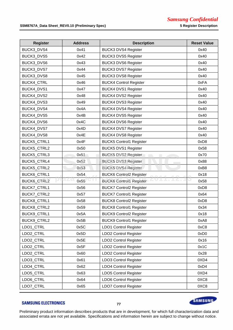
Samsung Confidential S5M8767A_Data Sheet_REV0.10 (Preliminary Spec) 5 Register Description
77
Preliminary product information describes products that are in development, for which full characterization data and
associated errata are not yet available. Specifications and information herein are subject to change without notice.
Register Address Description Reset Value
BUCK3_DVS4 0x41 BUCK3 DVS4 Register 0x40
BUCK3_DVS5 0x42 BUCK3 DVS5 Register 0x40
BUCK3_DVS6 0x43 BUCK3 DVS6 Register 0x40
BUCK3_DVS7 0x44 BUCK3 DVS7 Register 0x40
BUCK3_DVS8 0x45 BUCK3 DVS8 Register 0x40
BUCK4_CTRL 0x46 BUCK4 Control Register 0xFA
BUCK4_DVS1 0x47 BUCK4 DVS1 Register 0x40
BUCK4_DVS2 0x48 BUCK4 DVS2 Register 0x40
BUCK4_DVS3 0x49 BUCK4 DVS3 Register 0x40
BUCK4_DVS4 0x4A BUCK4 DVS4 Register 0x40
BUCK4_DVS5 0x4B BUCK4 DVS5 Register 0x40
BUCK4_DVS6 0x4C BUCK4 DVS6 Register 0x40
BUCK4_DVS7 0x4D BUCK4 DVS7 Register 0x40
BUCK4_DVS8 0x4E BUCK4 DVS8 Register 0x40
BUCK5_CTRL1 0x4F BUCK5 Control1 Register 0xD8
BUCK5_CTRL2 0x50 BUCK5 DVS1 Register 0x58
BUCK5_CTRL3 0x51 BUCK5 DVS2 Register 0x70
BUCK5_CTRL4 0x52 BUCK5 DVS3 Register 0x88
BUCK5_CTRL2 0x53 BUCK5 DVS4 Register 0xB8
BUCK6_CTRL1 0x54 BUCK6 Control2 Register 0x18
BUCK6_CTRL2 0x55 BUCK6 Control1 Register 0x58
BUCK7_CTRL1 0x56 BUCK7 Control2 Register 0xD8
BUCK7_CTRL2 0x57 BUCK7 Control1 Register 0x64
BUCK8_CTRL1 0x58 BUCK8 Control2 Register 0xD8
BUCK8_CTRL2 0x59 BUCK8 Control1 Register 0x34
BUCK9_CTRL1 0x5A BUCK9 Control2 Register 0x18
BUCK9_CTRL2 0x5B BUCK9 Control1 Register 0xA8
LDO1_CTRL 0x5C LDO1 Control Register 0xC8
LDO2_CTRL 0x5D LDO2 Control Register 0xD0
LDO2_CTRL 0x5E LDO2 Control Register 0x16
LDO2_CTRL 0x5F LDO2 Control Register 0x1C
LDO2_CTRL 0x60 LDO2 Control Register 0x28
LDO3_CTRL 0x61 LDO3 Control Register 0XD4
LDO4_CTRL 0x62 LDO4 Control Register 0xD4
LDO5_CTRL 0x63 LDO5 Control Register 0XD4
LDO6_CTRL 0x64 LDO6 Control Register 0XC8
LDO7_CTRL 0x65 LDO7 Control Register 0XC8
si-plaza / Jeff_cui at 14:14,2011.12.13
SAMSUNG

Samsung Confidential S5M8767A_Data Sheet_REV0.10 (Preliminary Spec) 5 Register Description
78
Preliminary product information describes products that are in development, for which full characterization data and
associated errata are not yet available. Specifications and information herein are subject to change without notice.
Register Address Description Reset Value
LDO8_CTRL 0x66 LDO8 Control Register 0XC8
LDO9_CTRL 0x67 LDO9 Control Register 0x2C
LDO10_CTRL 0x68 LDO10 Control Register 0XD4
LDO11_CTRL 0x69 LDO11 Control Register 0XD4
LDO12_CTRL 0x6A LDO12 Control Register 0XEC
LDO13_CTRL 0x6B LDO13 Control Register 0XD4
LDO14_CTRL 0x6C LDO14 Control Register 0XD4
LDO15_CTRL 0x6D LDO15 Control Register 0XC8
LDO16_CTRL 0x6E LDO16 Control Register 0xD4
LDO17_CTRL 0x6F LDO17 Control Register 0xE8
LDO18_CTRL 0x70 LDO18 Control Register 0x28
LDO19_CTRL 0x71 LDO19 Control Register 0x2C
LDO20_CTRL 0x72 LDO20 Control Register 0x2C
LDO21_CTRL 0x73 LDO21 Control Register 0x2C
LDO22_CTRL 0x74 LDO22 Control Register 0x32
LDO23_CTRL 0x75 LDO23 Control Register 0x28
LDO24_CTRL 0x76 LDO24 Control Register 0x2C
LDO25_CTRL 0x77 LDO25 Control Register 0x08
LDO26_CTRL 0x78 LDO26 Control Register 0x14
LDO27_CTRL 0x79 LDO27 Control Register 0x14
LDO28_CTRL 0x7A LDO28 Control Register 0x14
PWRONSRC 0xE0 Power on source Register N/A
si-plaza / Jeff_cui at 14:14,2011.12.13
SAMSUNG
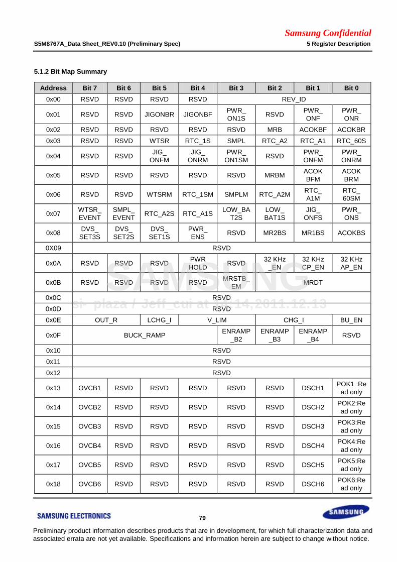
Samsung Confidential S5M8767A_Data Sheet_REV0.10 (Preliminary Spec) 5 Register Description
79
Preliminary product information describes products that are in development, for which full characterization data and
associated errata are not yet available. Specifications and information herein are subject to change without notice.
5.1.2 Bit Map Summary
Address Bit 7 Bit 6 Bit 5 Bit 4 Bit 3 Bit 2 Bit 1 Bit 0
0x00 RSVD RSVD RSVD RSVD REV_ID
0x01 RSVD RSVD JIGONBR JIGONBF PWR_
ON1S RSVD
PWR_
ONF
PWR_
ONR
0x02 RSVD RSVD RSVD RSVD RSVD MRB ACOKBF ACOKBR
0x03 RSVD RSVD WTSR RTC_1S SMPL RTC_A2 RTC_A1 RTC_60S
0x04 RSVD RSVD JIG_
ONFM
JIG_
ONRM
PWR_
ON1SM RSVD
PWR_
ONFM
PWR_
ONRM
0x05 RSVD RSVD RSVD RSVD RSVD MRBM ACOK
BFM
ACOK
BRM
0x06 RSVD RSVD WTSRM RTC_1SM SMPLM RTC_A2M RTC_
A1M
RTC_
60SM
0x07 WTSR_
EVENT
SMPL_
EVENT RTC_A2S RTC_A1S
LOW_BA
T2S
LOW_
BAT1S
JIG_
ONFS
PWR_
ONS
0x08 DVS_
SET3S
DVS_
SET2S
DVS_
SET1S
PWR_
ENS RSVD MR2BS MR1BS ACOKBS
0X09 RSVD
0x0A RSVD RSVD RSVD PWR
HOLD RSVD
32 KHz
_EN
32 KHz
CP_EN
32 KHz
AP_EN
0x0B RSVD RSVD RSVD RSVD MRSTB_
EM MRDT
0x0C RSVD
0x0D RSVD
0x0E OUT_R LCHG_I V_LIM CHG_I BU_EN
0x0F BUCK_RAMP ENRAMP
_B2
ENRAMP
_B3
ENRAMP
_B4 RSVD
0x10 RSVD
0x11 RSVD
0x12 RSVD
0x13 OVCB1 RSVD RSVD RSVD RSVD RSVD DSCH1 POK1 :Re
ad only
0x14 OVCB2 RSVD RSVD RSVD RSVD RSVD DSCH2 POK2:Re
ad only
0x15 OVCB3 RSVD RSVD RSVD RSVD RSVD DSCH3 POK3:Re
ad only
0x16 OVCB4 RSVD RSVD RSVD RSVD RSVD DSCH4 POK4:Re
ad only
0x17 OVCB5 RSVD RSVD RSVD RSVD RSVD DSCH5 POK5:Re
ad only
0x18 OVCB6 RSVD RSVD RSVD RSVD RSVD DSCH6 POK6:Re
ad only
si-plaza / Jeff_cui at 14:14,2011.12.13
SAMSUNG

Samsung Confidential S5M8767A_Data Sheet_REV0.10 (Preliminary Spec) 5 Register Description
80
Preliminary product information describes products that are in development, for which full characterization data and
associated errata are not yet available. Specifications and information herein are subject to change without notice.
Address Bit 7 Bit 6 Bit 5 Bit 4 Bit 3 Bit 2 Bit 1 Bit 0
0x19 OVCB7 RSVD RSVD RSVD RSVD RSVD DSCH7 POK7:Re
ad only
0x1A OVCB8 RSVD RSVD RSVD RSVD RSVD DSCH8 POK8:Re
ad only
0x1B OVCB9 RSVD RSVD RSVD RSVD RSVD DSCH9 POK9:Re
ad only
0x1C OVCB10 RSVD RSVD RSVD RSVD RSVD DSCH10 POK10:R
ead only
0x1D OVCB11 RSVD RSVD RSVD RSVD RSVD DSCH11 POK11:R
ead only
0x1E OVCB12 RSVD RSVD RSVD RSVD RSVD DSCH12 POK12:R
ead only
0x1F OVCB13 RSVD RSVD RSVD RSVD RSVD DSCH13 POK13:R
ead only
0x20 OVCB14 RSVD RSVD RSVD RSVD RSVD DSCH14 POK14:R
ead only
0x21 OVCB15 RSVD RSVD RSVD RSVD RSVD DSCH15 POK15:R
ead only
0x22 OVCB16 RSVD RSVD RSVD RSVD RSVD DSCH16 POK16:R
ead only
0x23 OVCB17 RSVD RSVD RSVD RSVD RSVD DSCH17 POK17:R
ead only
0x24 OVCB18 RSVD RSVD RSVD RSVD RSVD DSCH18 POK18:R
ead only
0x25 OVCB19 RSVD RSVD RSVD RSVD RSVD DSCH19 POK19:R
ead only
0x26 OVCB20 RSVD RSVD RSVD RSVD RSVD DSCH20 POK20:R
ead only
0x27 OVCB21 RSVD RSVD RSVD RSVD RSVD DSCH21 POK21:R
ead only
0x28 OVCB22 RSVD RSVD RSVD RSVD RSVD DSCH22 POK22:R
ead only
0x29 OVCB23 RSVD RSVD RSVD RSVD RSVD DSCH23 POK23:R
ead only
0x2A OVCB24 RSVD RSVD RSVD RSVD RSVD DSCH24 POK24:R
ead only
0x2B OVCB25 RSVD RSVD RSVD RSVD RSVD DSCH25 POK25:R
ead only
0x2C OVCB26 RSVD RSVD RSVD RSVD RSVD DSCH26 POK26:R
ead only
0x2D OVCB27 RSVD RSVD RSVD RSVD RSVD DSCH27 POK27:R
ead only
0x2E OVCB28 RSVD RSVD RSVD RSVD RSVD DSCH28 POK28:R
si-plaza / Jeff_cui at 14:14,2011.12.13
SAMSUNG
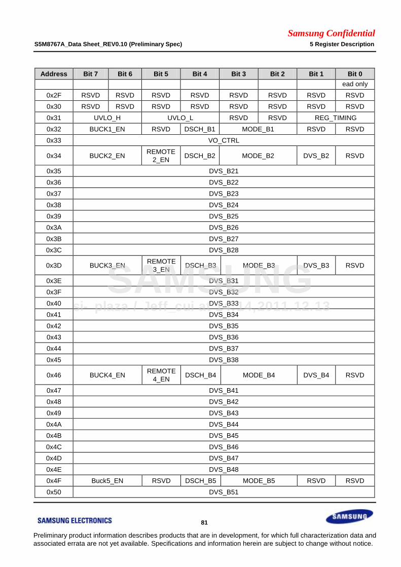
Samsung Confidential S5M8767A_Data Sheet_REV0.10 (Preliminary Spec) 5 Register Description
81
Preliminary product information describes products that are in development, for which full characterization data and
associated errata are not yet available. Specifications and information herein are subject to change without notice.
Address Bit 7 Bit 6 Bit 5 Bit 4 Bit 3 Bit 2 Bit 1 Bit 0
ead only
0x2F RSVD RSVD RSVD RSVD RSVD RSVD RSVD RSVD
0x30 RSVD RSVD RSVD RSVD RSVD RSVD RSVD RSVD
0x31 UVLO_H UVLO_L RSVD RSVD REG_TIMING
0x32 BUCK1_EN RSVD DSCH_B1 MODE_B1 RSVD RSVD
0x33 VO_CTRL
0x34 BUCK2_EN REMOTE
2_EN DSCH_B2 MODE_B2 DVS_B2 RSVD
0x35 DVS_B21
0x36 DVS_B22
0x37 DVS_B23
0x38 DVS_B24
0x39 DVS_B25
0x3A DVS_B26
0x3B DVS_B27
0x3C DVS_B28
0x3D BUCK3_EN REMOTE
3_EN DSCH_B3 MODE_B3 DVS_B3 RSVD
0x3E DVS_B31
0x3F DVS_B32
0x40 DVS_B33
0x41 DVS_B34
0x42 DVS_B35
0x43 DVS_B36
0x44 DVS_B37
0x45 DVS_B38
0x46 BUCK4_EN REMOTE
4_EN DSCH_B4 MODE_B4 DVS_B4 RSVD
0x47 DVS_B41
0x48 DVS_B42
0x49 DVS_B43
0x4A DVS_B44
0x4B DVS_B45
0x4C DVS_B46
0x4D DVS_B47
0x4E DVS_B48
0x4F Buck5_EN RSVD DSCH_B5 MODE_B5 RSVD RSVD
0x50 DVS_B51
si-plaza / Jeff_cui at 14:14,2011.12.13
SAMSUNG
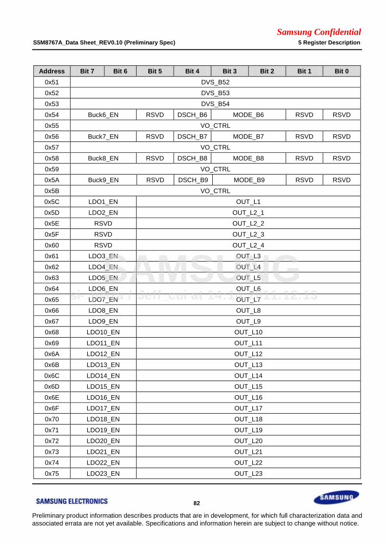
Samsung Confidential S5M8767A_Data Sheet_REV0.10 (Preliminary Spec) 5 Register Description
82
Preliminary product information describes products that are in development, for which full characterization data and
associated errata are not yet available. Specifications and information herein are subject to change without notice.
Address Bit 7 Bit 6 Bit 5 Bit 4 Bit 3 Bit 2 Bit 1 Bit 0
0x51 DVS_B52
0x52 DVS_B53
0x53 DVS_B54
0x54 Buck6_EN RSVD DSCH_B6 MODE_B6 RSVD RSVD
0x55 VO_CTRL
0x56 Buck7_EN RSVD DSCH_B7 MODE_B7 RSVD RSVD
0x57 VO_CTRL
0x58 Buck8_EN RSVD DSCH_B8 MODE_B8 RSVD RSVD
0x59 VO_CTRL
0x5A Buck9_EN RSVD DSCH_B9 MODE_B9 RSVD RSVD
0x5B VO_CTRL
0x5C LDO1_EN OUT_L1
0x5D LDO2_EN OUT_L2_1
0x5E RSVD OUT_L2_2
0x5F RSVD OUT_L2_3
0x60 RSVD OUT_L2_4
0x61 LDO3_EN OUT_L3
0x62 LDO4_EN OUT_L4
0x63 LDO5_EN OUT_L5
0x64 LDO6_EN OUT_L6
0x65 LDO7_EN OUT_L7
0x66 LDO8_EN OUT_L8
0x67 LDO9_EN OUT_L9
0x68 LDO10_EN OUT_L10
0x69 LDO11_EN OUT_L11
0x6A LDO12_EN OUT_L12
0x6B LDO13_EN OUT_L13
0x6C LDO14_EN OUT_L14
0x6D LDO15_EN OUT_L15
0x6E LDO16_EN OUT_L16
0x6F LDO17_EN OUT_L17
0x70 LDO18_EN OUT_L18
0x71 LDO19_EN OUT_L19
0x72 LDO20_EN OUT_L20
0x73 LDO21_EN OUT_L21
0x74 LDO22_EN OUT_L22
0x75 LDO23_EN OUT_L23
si-plaza / Jeff_cui at 14:14,2011.12.13
SAMSUNG
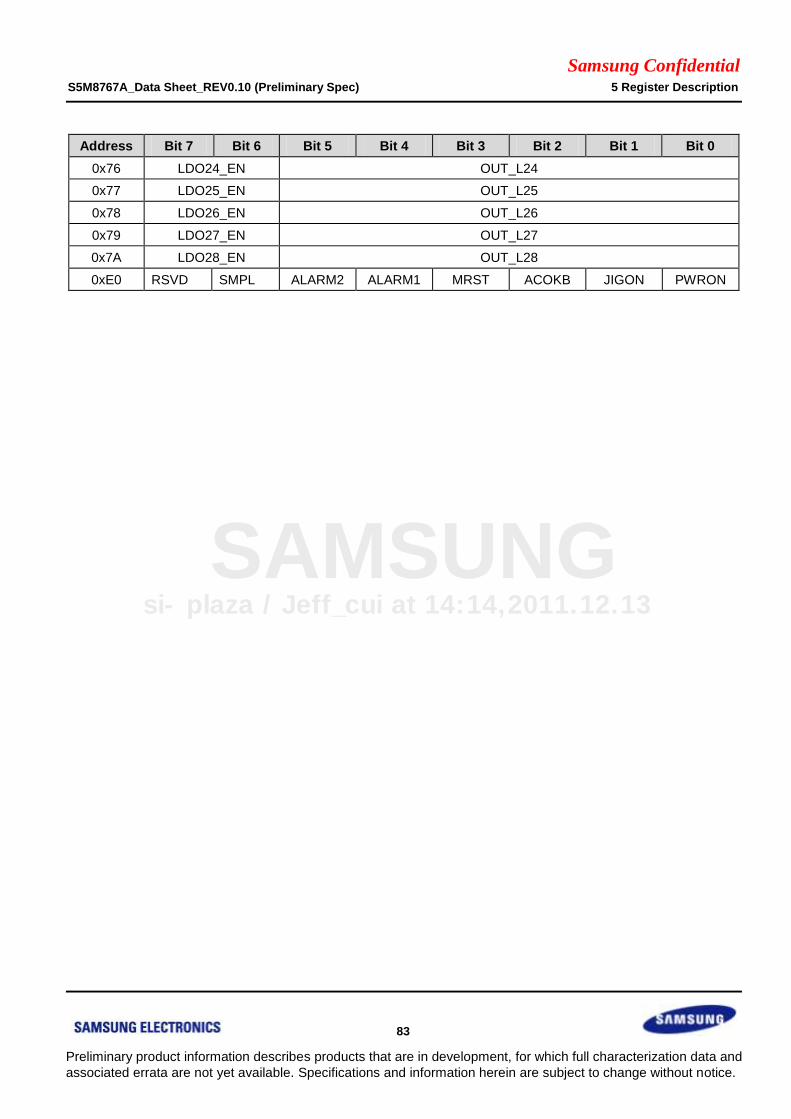
Samsung Confidential S5M8767A_Data Sheet_REV0.10 (Preliminary Spec) 5 Register Description
83
Preliminary product information describes products that are in development, for which full characterization data and
associated errata are not yet available. Specifications and information herein are subject to change without notice.
Address Bit 7 Bit 6 Bit 5 Bit 4 Bit 3 Bit 2 Bit 1 Bit 0
0x76 LDO24_EN OUT_L24
0x77 LDO25_EN OUT_L25
0x78 LDO26_EN OUT_L26
0x79 LDO27_EN OUT_L27
0x7A LDO28_EN OUT_L28
0xE0 RSVD SMPL ALARM2 ALARM1 MRST ACOKB JIGON PWRON
si-plaza / Jeff_cui at 14:14,2011.12.13
SAMSUNG
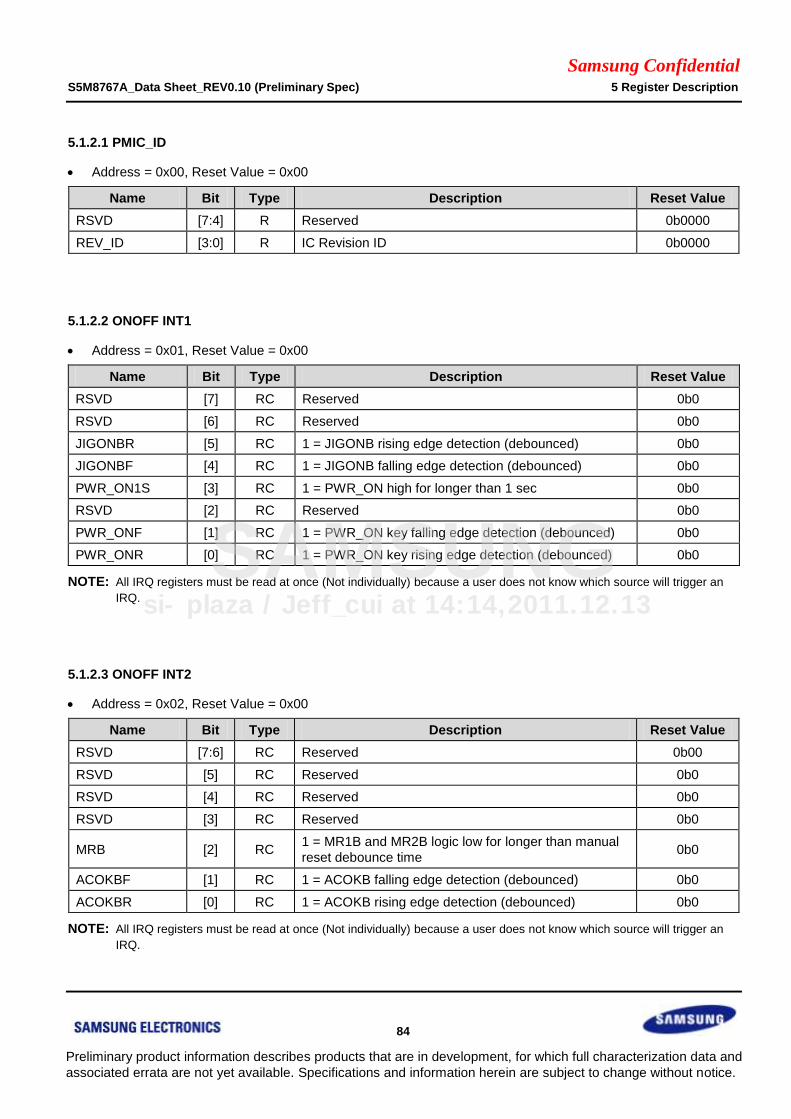
Samsung Confidential S5M8767A_Data Sheet_REV0.10 (Preliminary Spec) 5 Register Description
84
Preliminary product information describes products that are in development, for which full characterization data and
associated errata are not yet available. Specifications and information herein are subject to change without notice.
5.1.2.1 PMIC_ID
Address = 0x00, Reset Value = 0x00
Name Bit Type Description Reset Value
RSVD [7:4] R Reserved 0b0000
REV_ID [3:0] R IC Revision ID 0b0000
5.1.2.2 ONOFF INT1
Address = 0x01, Reset Value = 0x00
Name Bit Type Description Reset Value
RSVD [7] RC Reserved 0b0
RSVD [6] RC Reserved 0b0
JIGONBR [5] RC 1 = JIGONB rising edge detection (debounced) 0b0
JIGONBF [4] RC 1 = JIGONB falling edge detection (debounced) 0b0
PWR_ON1S [3] RC 1 = PWR_ON high for longer than 1 sec 0b0
RSVD [2] RC Reserved 0b0
PWR_ONF [1] RC 1 = PWR_ON key falling edge detection (debounced) 0b0
PWR_ONR [0] RC 1 = PWR_ON key rising edge detection (debounced) 0b0
NOTE: All IRQ registers must be read at once (Not individually) because a user does not know which source will trigger an
IRQ.
5.1.2.3 ONOFF INT2
Address = 0x02, Reset Value = 0x00
Name Bit Type Description Reset Value
RSVD [7:6] RC Reserved 0b00
RSVD [5] RC Reserved 0b0
RSVD [4] RC Reserved 0b0
RSVD [3] RC Reserved 0b0
MRB [2] RC 1 = MR1B and MR2B logic low for longer than manual
reset debounce time 0b0
ACOKBF [1] RC 1 = ACOKB falling edge detection (debounced) 0b0
ACOKBR [0] RC 1 = ACOKB rising edge detection (debounced) 0b0
NOTE: All IRQ registers must be read at once (Not individually) because a user does not know which source will trigger an
IRQ.
si-plaza / Jeff_cui at 14:14,2011.12.13
SAMSUNG
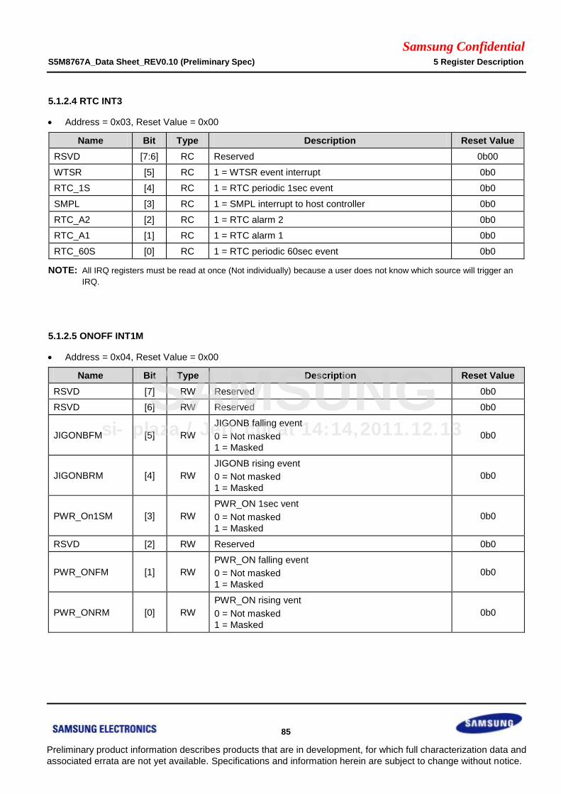
Samsung Confidential S5M8767A_Data Sheet_REV0.10 (Preliminary Spec) 5 Register Description
85
Preliminary product information describes products that are in development, for which full characterization data and
associated errata are not yet available. Specifications and information herein are subject to change without notice.
5.1.2.4 RTC INT3
Address = 0x03, Reset Value = 0x00
Name Bit Type Description Reset Value
RSVD [7:6] RC Reserved 0b00
WTSR [5] RC 1 = WTSR event interrupt 0b0
RTC_1S [4] RC 1 = RTC periodic 1sec event 0b0
SMPL [3] RC 1 = SMPL interrupt to host controller 0b0
RTC_A2 [2] RC 1 = RTC alarm 2 0b0
RTC_A1 [1] RC 1 = RTC alarm 1 0b0
RTC_60S [0] RC 1 = RTC periodic 60sec event 0b0
NOTE: All IRQ registers must be read at once (Not individually) because a user does not know which source will trigger an
IRQ.
5.1.2.5 ONOFF INT1M
Address = 0x04, Reset Value = 0x00
Name Bit Type Description Reset Value
RSVD [7] RW Reserved 0b0
RSVD [6] RW Reserved 0b0
JIGONBFM [5] RW
JIGONB falling event
0 = Not masked
1 = Masked
0b0
JIGONBRM [4] RW
JIGONB rising event
0 = Not masked
1 = Masked
0b0
PWR_On1SM [3] RW
PWR_ON 1sec vent
0 = Not masked
1 = Masked
0b0
RSVD [2] RW Reserved 0b0
PWR_ONFM [1] RW
PWR_ON falling event
0 = Not masked
1 = Masked
0b0
PWR_ONRM [0] RW
PWR_ON rising vent
0 = Not masked
1 = Masked
0b0
si-plaza / Jeff_cui at 14:14,2011.12.13
SAMSUNG
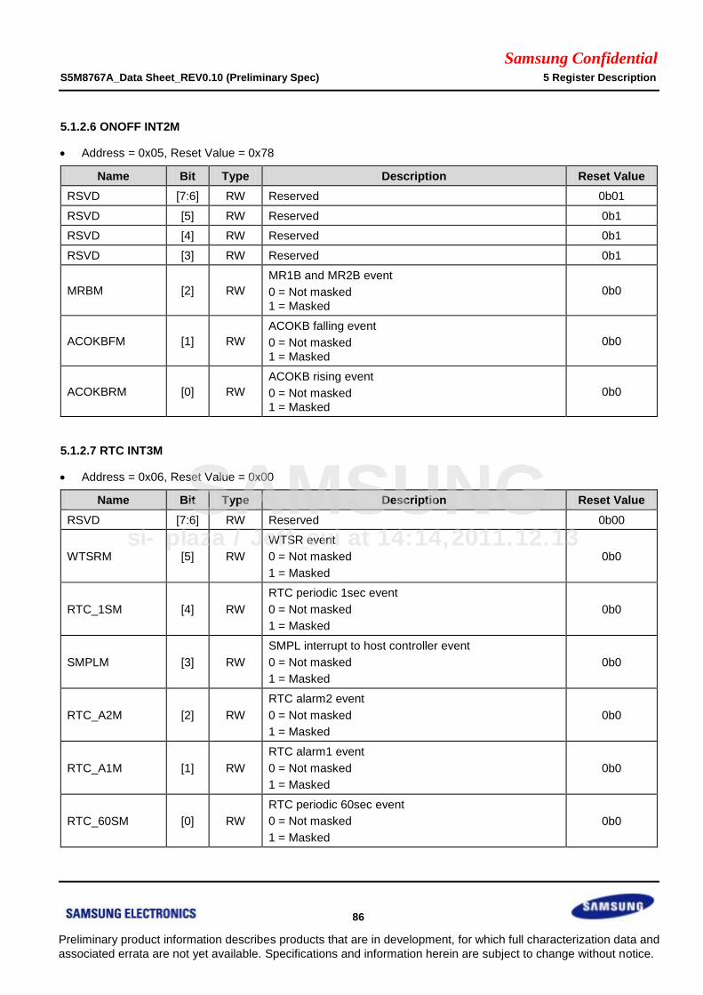
Samsung Confidential S5M8767A_Data Sheet_REV0.10 (Preliminary Spec) 5 Register Description
86
Preliminary product information describes products that are in development, for which full characterization data and
associated errata are not yet available. Specifications and information herein are subject to change without notice.
5.1.2.6 ONOFF INT2M
Address = 0x05, Reset Value = 0x78
Name Bit Type Description Reset Value
RSVD [7:6] RW Reserved 0b01
RSVD [5] RW Reserved 0b1
RSVD [4] RW Reserved 0b1
RSVD [3] RW Reserved 0b1
MRBM [2] RW
MR1B and MR2B event
0 = Not masked
1 = Masked
0b0
ACOKBFM [1] RW
ACOKB falling event
0 = Not masked
1 = Masked
0b0
ACOKBRM [0] RW
ACOKB rising event
0 = Not masked
1 = Masked
0b0
5.1.2.7 RTC INT3M
Address = 0x06, Reset Value = 0x00
Name Bit Type Description Reset Value
RSVD [7:6] RW Reserved 0b00
WTSRM [5] RW
WTSR event
0 = Not masked
1 = Masked
0b0
RTC_1SM [4] RW
RTC periodic 1sec event
0 = Not masked
1 = Masked
0b0
SMPLM [3] RW
SMPL interrupt to host controller event
0 = Not masked
1 = Masked
0b0
RTC_A2M [2] RW
RTC alarm2 event
0 = Not masked
1 = Masked
0b0
RTC_A1M [1] RW
RTC alarm1 event
0 = Not masked
1 = Masked
0b0
RTC_60SM [0] RW
RTC periodic 60sec event
0 = Not masked
1 = Masked
0b0
si-plaza / Jeff_cui at 14:14,2011.12.13
SAMSUNG
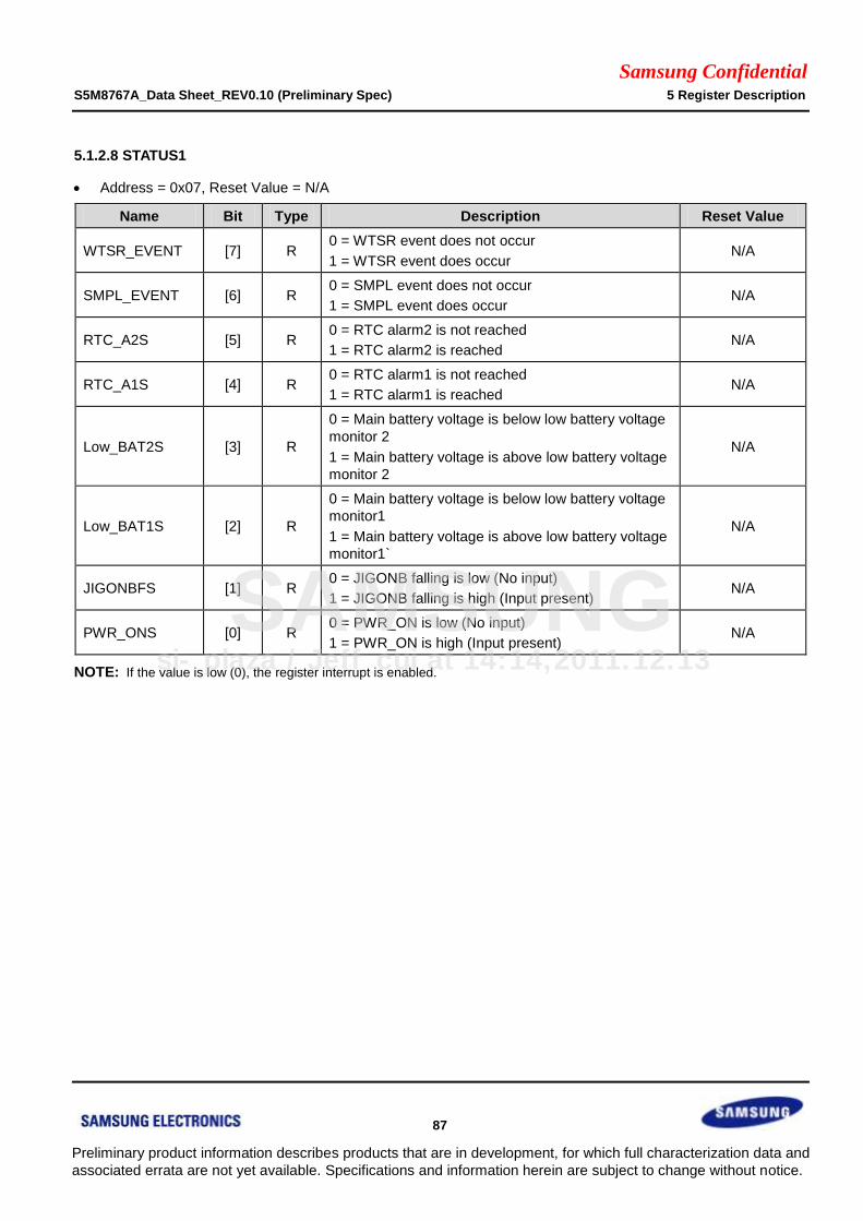
Samsung Confidential S5M8767A_Data Sheet_REV0.10 (Preliminary Spec) 5 Register Description
87
Preliminary product information describes products that are in development, for which full characterization data and
associated errata are not yet available. Specifications and information herein are subject to change without notice.
5.1.2.8 STATUS1
Address = 0x07, Reset Value = N/A
Name Bit Type Description Reset Value
WTSR_EVENT [7] R 0 = WTSR event does not occur
1 = WTSR event does occur N/A
SMPL_EVENT [6] R 0 = SMPL event does not occur
1 = SMPL event does occur N/A
RTC_A2S [5] R 0 = RTC alarm2 is not reached
1 = RTC alarm2 is reached N/A
RTC_A1S [4] R 0 = RTC alarm1 is not reached
1 = RTC alarm1 is reached N/A
Low_BAT2S [3] R
0 = Main battery voltage is below low battery voltage
monitor 2
1 = Main battery voltage is above low battery voltage
monitor 2
N/A
Low_BAT1S [2] R
0 = Main battery voltage is below low battery voltage
monitor1
1 = Main battery voltage is above low battery voltage
monitor1`
N/A
JIGONBFS [1] R 0 = JIGONB falling is low (No input)
1 = JIGONB falling is high (Input present) N/A
PWR_ONS [0] R 0 = PWR_ON is low (No input)
1 = PWR_ON is high (Input present) N/A
NOTE: If the value is low (0), the register interrupt is enabled. si-plaza / Jeff_cui at 14:14,2011.12.13
SAMSUNG
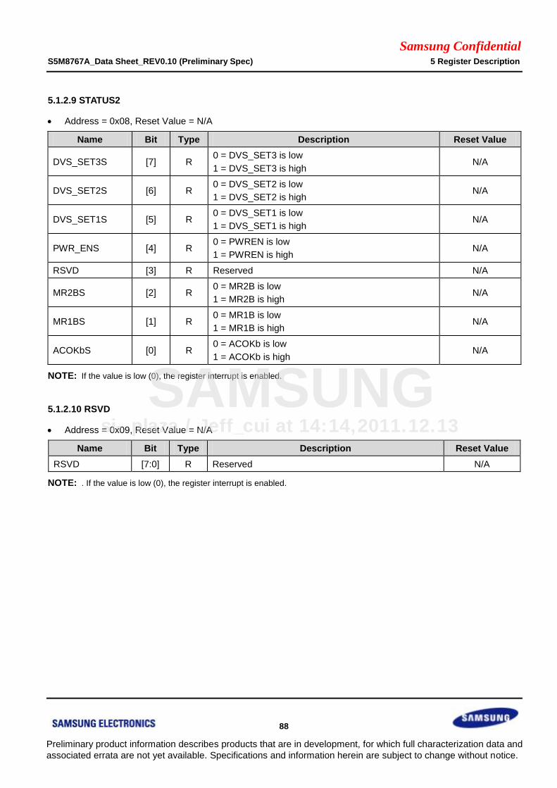
Samsung Confidential S5M8767A_Data Sheet_REV0.10 (Preliminary Spec) 5 Register Description
88
Preliminary product information describes products that are in development, for which full characterization data and
associated errata are not yet available. Specifications and information herein are subject to change without notice.
5.1.2.9 STATUS2
Address = 0x08, Reset Value = N/A
Name Bit Type Description Reset Value
DVS_SET3S [7] R 0 = DVS_SET3 is low
1 = DVS_SET3 is high N/A
DVS_SET2S [6] R 0 = DVS_SET2 is low
1 = DVS_SET2 is high N/A
DVS_SET1S [5] R 0 = DVS_SET1 is low
1 = DVS_SET1 is high N/A
PWR_ENS [4] R 0 = PWREN is low
1 = PWREN is high N/A
RSVD [3] R Reserved N/A
MR2BS [2] R 0 = MR2B is low
1 = MR2B is high N/A
MR1BS [1] R 0 = MR1B is low
1 = MR1B is high N/A
ACOKbS [0] R 0 = ACOKb is low
1 = ACOKb is high N/A
NOTE: If the value is low (0), the register interrupt is enabled.
5.1.2.10 RSVD
Address = 0x09, Reset Value = N/A
Name Bit Type Description Reset Value
RSVD [7:0] R Reserved N/A
NOTE: . If the value is low (0), the register interrupt is enabled.
si-plaza / Jeff_cui at 14:14,2011.12.13
SAMSUNG

Samsung Confidential S5M8767A_Data Sheet_REV0.10 (Preliminary Spec) 5 Register Description
89
Preliminary product information describes products that are in development, for which full characterization data and
associated errata are not yet available. Specifications and information herein are subject to change without notice.
5.1.2.11 CTRL1
Address = 0x0A, Reset Value = 0x01
Name Bit Type Description Reset Value
RSVD [7:5] RW Reserved 0b000
PWRHOLD [4] RW
Internal PWRHOLD logic and external PWRHOLD
signal are ORed
0 = Internal PWRHOLD logic is low
1 = Internal PWRHOLD logic is high
0b0
RSVD [3] RW Reserved 0b0
32KHzBT_EN [1] RW 0 = Turn 32 kHz BT on
1 = Turn 32 kHz BT off 0b0
32KHzCP_EN [1] RW 0 = Turn 32 kHz CP on
1 = Turn 32 kHz CP off 0b0
32KHzAP_EN [0] RW 0 = Turn 32 kHz AP on
1 = Turn 32 kHz AP off 0b1
5.1.2.12 CTRL2
Address = 0x0B, Reset Value = 0x0E
Name Bit Type Description Reset Value
RSVD [7:4] RW Reserved 0b0000
MRSTB_EN [3] RW 0 = Manual Resetb disable
1 = Manual Resetb enable 0b1
MRDT [2:0] RW
Manual Reset Debounce Timer when MR1B = MR2B =
low
000 = 9 sec
001 = 10 sec
010 = 3 sec
011 = 4 sec
100 = 5 sec
101 = 6 sec
110 = 7 sec (Default)
111 = 8 sec
0b110
5.1.2.13 RSVD
Address = 0x0C, Reset Value = 0xE7
Name Bit Type Description Reset Value
RSVD [7:0] R Reserved N/A
si-plaza / Jeff_cui at 14:14,2011.12.13
SAMSUNG
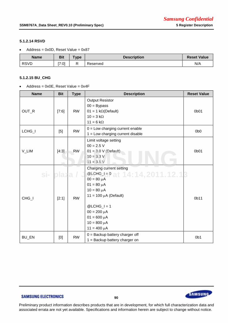
Samsung Confidential S5M8767A_Data Sheet_REV0.10 (Preliminary Spec) 5 Register Description
90
Preliminary product information describes products that are in development, for which full characterization data and
associated errata are not yet available. Specifications and information herein are subject to change without notice.
5.1.2.14 RSVD
Address = 0x0D, Reset Value = 0x87
Name Bit Type Description Reset Value
RSVD [7:0] R Reserved N/A
5.1.2.15 BU_CHG
Address = 0x0E, Reset Value = 0x4F
Name Bit Type Description Reset Value
OUT_R [7:6] RW
Output Resistor
00 = Bypass
01 = 1 k(Default)
10 = 3 k
11 = 6 k
0b01
LCHG_I [5] RW 0 = Low charging current enable
1 = Low charging current disable 0b0
V_LIM [4:3] RW
Limit voltage setting
00 = 2.5 V
01 = 3.0 V (Default)
10 = 3.3 V
11 = 3.5 V
0b01
CHG_I [2:1] RW
Charging current setting
@LCHG_I = 0
00 = 80 A
01 = 80 A
10 = 80 A
11 = 100 A (Default)
@LCHG_I = 1
00 = 200 A
01 = 600 A
10 = 800 A
11 = 400 A
0b11
BU_EN [0] RW 0 = Backup battery charger off
1 = Backup battery charger on 0b1
si-plaza / Jeff_cui at 14:14,2011.12.13
SAMSUNG
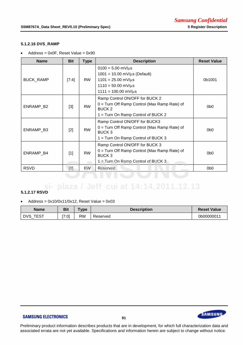
Samsung Confidential S5M8767A_Data Sheet_REV0.10 (Preliminary Spec) 5 Register Description
91
Preliminary product information describes products that are in development, for which full characterization data and
associated errata are not yet available. Specifications and information herein are subject to change without notice.
5.1.2.16 DVS_RAMP
Address = 0x0F, Reset Value = 0x90
Name Bit Type Description Reset Value
BUCK_RAMP [7:4] RW
0100 = 5.00 mV/s
1001 = 10.00 mV/s (Default)
1101 = 25.00 mV/s
1110 = 50.00 mV/s
1111 = 100.00 mV/s
0b1001
ENRAMP_B2 [3] RW
Ramp Control ON/OFF for BUCK 2
0 = Turn Off Ramp Control (Max Ramp Rate) of
BUCK 2
1 = Turn On Ramp Control of BUCK 2
0b0
ENRAMP_B3 [2] RW
Ramp Control ON/OFF for BUCK3
0 = Turn Off Ramp Control (Max Ramp Rate) of
BUCK 3
1 = Turn On Ramp Control of BUCK 3
0b0
ENRAMP_B4 [1] RW
Ramp Control ON/OFF for BUCK 3
0 = Turn Off Ramp Control (Max Ramp Rate) of
BUCK 3
1 = Turn On Ramp Control of BUCK 3
0b0
RSVD [0] RW Reserved 0b0
5.1.2.17 RSVD
Address = 0x10/0x11/0x12, Reset Value = 0x03
Name Bit Type Description Reset Value
DVS_TEST [7:0] RW Reserved 0b00000011
si-plaza / Jeff_cui at 14:14,2011.12.13
SAMSUNG
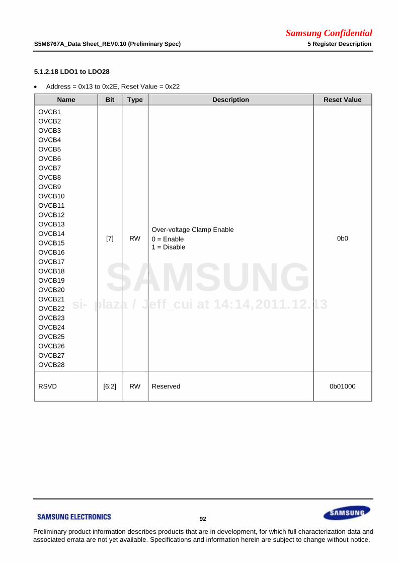
Samsung Confidential S5M8767A_Data Sheet_REV0.10 (Preliminary Spec) 5 Register Description
92
Preliminary product information describes products that are in development, for which full characterization data and
associated errata are not yet available. Specifications and information herein are subject to change without notice.
5.1.2.18 LDO1 to LDO28
Address = 0x13 to 0x2E, Reset Value = 0x22
Name Bit Type Description Reset Value
OVCB1
OVCB2
OVCB3
OVCB4
OVCB5
OVCB6
OVCB7
OVCB8
OVCB9
OVCB10
OVCB11
OVCB12
OVCB13
OVCB14
OVCB15
OVCB16
OVCB17
OVCB18
OVCB19
OVCB20
OVCB21
OVCB22
OVCB23
OVCB24
OVCB25
OVCB26
OVCB27
OVCB28
[7] RW
Over-voltage Clamp Enable
0 = Enable
1 = Disable
0b0
RSVD [6:2] RW Reserved 0b01000
si-plaza / Jeff_cui at 14:14,2011.12.13
SAMSUNG

Samsung Confidential S5M8767A_Data Sheet_REV0.10 (Preliminary Spec) 5 Register Description
93
Preliminary product information describes products that are in development, for which full characterization data and
associated errata are not yet available. Specifications and information herein are subject to change without notice.
Name Bit Type Description Reset Value
DSCH1
DSCH2
DSCH3
DSCH4
DSCH5
DSCH6
DSCH7
DSCH8
DSCH9
DSCH10
DSCH11
DSCH12
DSCH13
DSCH14
DSCH15
DSCH16
DSCH17
DSCH18
DSCH19
DSCH20
DSCH21
DSCH22
DSCH23
DSCH24
DSCH25
DSCH26
DSCH27
DSCH28
[1] RW
Active Discharge Enable
0 = Disable
1 = Enable
0b1
POK1: Read only
POK2: Read only
POK3: Read only
POK4: Read only
POK5: Read only
POK6: Read only
POK7: Read only
POK8: Read only
POK9: Read only
POK10: Read only
POK11: Read only
POK12: Read only
POK13: Read only
POK14: Read only
POK15: Read only
[0] RW
LDO output voltage OK flag bit
0 = LDO output is less than 90 % of target output
voltage (POK threshold), and the device is operating
in normal mode.
1 = LDO output is higher than the POK threshold, or
LDO is operating in low-power mode, or the device is
disabled.
0b0
si-plaza / Jeff_cui at 14:14,2011.12.13
SAMSUNG

Samsung Confidential S5M8767A_Data Sheet_REV0.10 (Preliminary Spec) 5 Register Description
94
Preliminary product information describes products that are in development, for which full characterization data and
associated errata are not yet available. Specifications and information herein are subject to change without notice.
Name Bit Type Description Reset Value
POK16: Read only
POK17: Read only
POK18: Read only
POK19: Read only
POK20: Read only
POK21: Read only
POK22: Read only
POK23: Read only
POK24: Read only
POK25: Read only
POK26: Read only
POK27: Read only
POK28: Read only
5.1.2.19 RSVD
Address = 0x2F/0x30, Reset Value = 0x00
Name Bit Type Description Reset Value
RSVD [7:0] RW Reserved 0b00000000
5.1.2.20 UVLO
Address = 0x31, Reset Value = 0x04
Name Bit Type Description Reset Value
UVLO_H [7:6] RW UVLO Rising Level Trimming 0b00
UVLO_L [5:4] RW UVLO Falling Level Trimming 0b00
RSVD [3] RW Reserved 0b0
RSVD [2] RW Reserved 0b1
REG_TIMING [1:0] RW Regulator Timing Trimming 0b00
si-plaza / Jeff_cui at 14:14,2011.12.13
SAMSUNG

Samsung Confidential S5M8767A_Data Sheet_REV0.10 (Preliminary Spec) 5 Register Description
95
Preliminary product information describes products that are in development, for which full characterization data and
associated errata are not yet available. Specifications and information herein are subject to change without notice.
5.1.2.21 BUCK1_CTRL1
Address = 0x32, Reset Value = 0xD8
Name Bit Type Description Reset Value
BUCK1_EN [7:6] RW
BUCK1 enable control
00 = Always off
01 = On/off by PWREN (High: On, Low: Off)
1x = Always on (Default)
0b11
RSVD [5] RW Reserved 0b0
DSCH_B1 [4] RW
Active Discharge of SW1
0 = No Active Discharge
1 = Active Discharge (Default)
0b1
MODE_B1 [3:2] RW
Mode Control
10 = Auto mode (Default)
11 = Forced PWM
0b10
RSVD [1] RW Reserved 0b0
RSVD [0] RW Reserved 0b0
5.1.2.22 BUCK1_CTRL2
Address = 0x33, Reset Value = 0x38
Name Bit Type Description Reset Value
VO_CTRL [7:0] RW
BUCK 1 Output Voltage Control
8-bit Programmable from 0.65 V to 2.225 V in 6.25
mV steps
0b00111000
si-plaza / Jeff_cui at 14:14,2011.12.13
SAMSUNG

Samsung Confidential S5M8767A_Data Sheet_REV0.10 (Preliminary Spec) 5 Register Description
96
Preliminary product information describes products that are in development, for which full characterization data and
associated errata are not yet available. Specifications and information herein are subject to change without notice.
5.1.2.23 BUCK2_CTRL
Address = 0x34, Reset Value = 0xFA
Name Bit Type Description Reset Value
BUCK2_EN [7:6] RW
BUCK2 enable control
00 = Always off
01 = On/off by PWREN (High: On, Low: Off)
10 = Reserved
11 = Always on (Default)
0b11
REMOTE2_EN [5] RW 0 = Turn Remote2_sense Off
1 = Turn Remote2_sense On (Default) 0b1
DSCH_B2 [4] RW
Active Discharge of SW2
0 = No Active Discharge
1 = Active Discharge (Default)
0b1
MODE_B2 [3:2] RW
Mode Control
10 = Auto mode (Default)
11 = Forced PWM
0b10
DVS_B2 [1] RW
DVS Control
0 = DVS Off
1 = DVS On (Output Voltage is chosen by SET1, SET2
and SET3)
0b1
RSVD [0] RW Reserved 0b0
5.1.2.24 BUCK2_DVS1 to BUCK2_DVS8
Address = 0x35 to 0x3C, Reset Value = 0x50
Name Bit Type Description Reset Value
DVS_B21
DVS_B22
DVS_B23
DVS_B24
DVS_B25
DVS_B26
DVS_B27
DVS_B28
[7:0] RW
BUCK2 DVS Output Voltage Option
8-bit Programmable from 0.6 V to 1.6 V in 6.25 mV
steps
0b01010000
si-plaza / Jeff_cui at 14:14,2011.12.13
SAMSUNG

Samsung Confidential S5M8767A_Data Sheet_REV0.10 (Preliminary Spec) 5 Register Description
97
Preliminary product information describes products that are in development, for which full characterization data and
associated errata are not yet available. Specifications and information herein are subject to change without notice.
5.1.2.25 BUCK3_CTRL
Address = 0x3D, Reset Value = 0xFA
Name Bit Type Description Reset Value
BUCK3_EN [7:6] RW
BUCK 3 enable control
00 = Always off
01 = On/off by PWREN (High:On, Low:Off)
10 = Reserved
11 = Always on (Default)
0b11
REMOTE3_EN [5] RW 0 = Turn Remote3_sense Off
1 = Turn Remote3_sense On (Default) 0b1
DSCH_B3 [4] RW
Active Discharge of SW3
0 = No Active Discharge
1 = Active Discharge (Default)
0b1
MODE_B3 [3:2] RW
Mode Control
10 = Auto Mode (Default)
11 = Forced PWM
0b10
DVS_B3 [1] RW
Dvs Control
0 = DVS Off
1 = DVS On (Output voltage is chosen by SET1, SET2
and SET3)
0b1
RSVD [0] RW Reserved 0b0
5.1.2.26 BUCK3_DVS1 to BUCK3_DVS8
Address = 0x3E to 0x45, Reset Value = 0x40
Name Bit Type Description Reset Value
DVS_B31
DVS_B32
DVS_B33
DVS_B34
DVS_B35
DVS_B36
DVS_B37
DVS_B38
[7:0] RW
BUCK 3 DVS Output Voltage Option
8-bit Programmable from 0.6 V to 1.6 V in 6.25 mV
steps
0b01000000
si-plaza / Jeff_cui at 14:14,2011.12.13
SAMSUNG
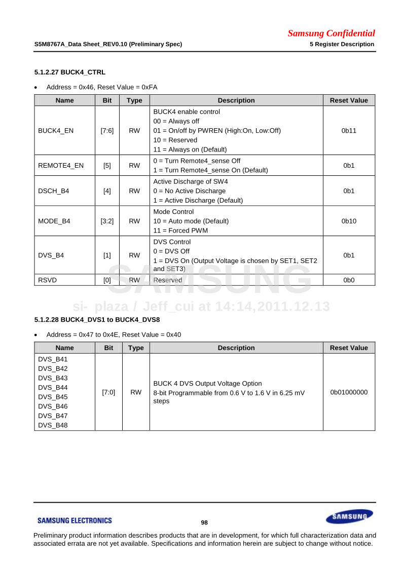
Samsung Confidential S5M8767A_Data Sheet_REV0.10 (Preliminary Spec) 5 Register Description
98
Preliminary product information describes products that are in development, for which full characterization data and
associated errata are not yet available. Specifications and information herein are subject to change without notice.
5.1.2.27 BUCK4_CTRL
Address = 0x46, Reset Value = 0xFA
Name Bit Type Description Reset Value
BUCK4_EN [7:6] RW
BUCK4 enable control
00 = Always off
01 = On/off by PWREN (High:On, Low:Off)
10 = Reserved
11 = Always on (Default)
0b11
REMOTE4_EN [5] RW 0 = Turn Remote4_sense Off
1 = Turn Remote4_sense On (Default) 0b1
DSCH_B4 [4] RW
Active Discharge of SW4
0 = No Active Discharge
1 = Active Discharge (Default)
0b1
MODE_B4 [3:2] RW
Mode Control
10 = Auto mode (Default)
11 = Forced PWM
0b10
DVS_B4 [1] RW
DVS Control
0 = DVS Off
1 = DVS On (Output Voltage is chosen by SET1, SET2
and SET3)
0b1
RSVD [0] RW Reserved 0b0
5.1.2.28 BUCK4_DVS1 to BUCK4_DVS8
Address = 0x47 to 0x4E, Reset Value = 0x40
Name Bit Type Description Reset Value
DVS_B41
DVS_B42
DVS_B43
DVS_B44
DVS_B45
DVS_B46
DVS_B47
DVS_B48
[7:0] RW
BUCK 4 DVS Output Voltage Option
8-bit Programmable from 0.6 V to 1.6 V in 6.25 mV
steps
0b01000000
si-plaza / Jeff_cui at 14:14,2011.12.13
SAMSUNG
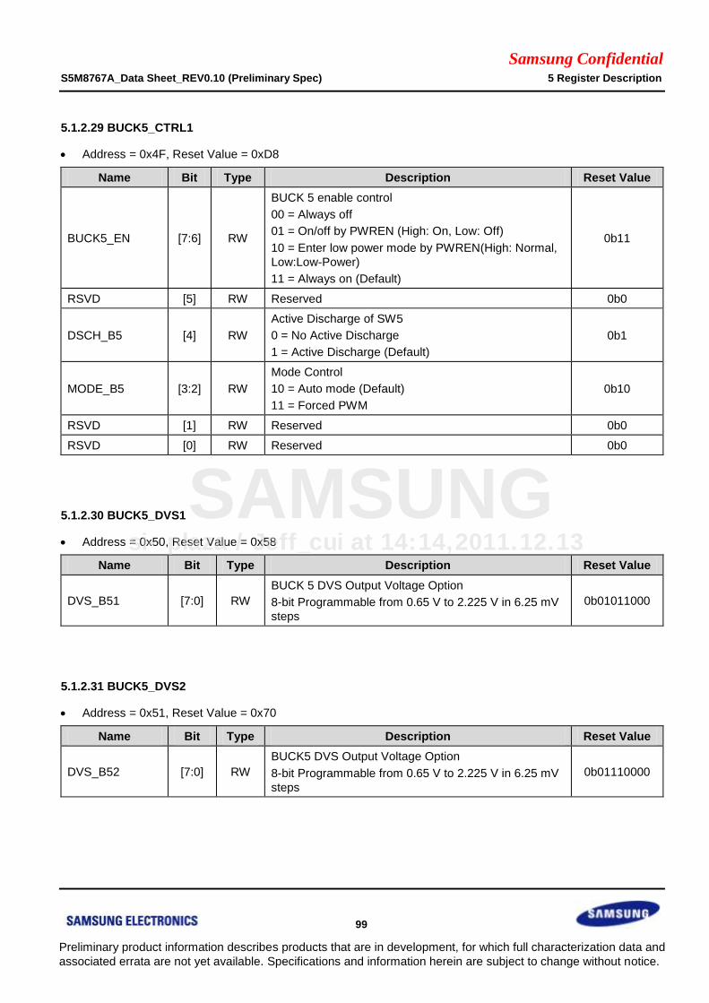
Samsung Confidential S5M8767A_Data Sheet_REV0.10 (Preliminary Spec) 5 Register Description
99
Preliminary product information describes products that are in development, for which full characterization data and
associated errata are not yet available. Specifications and information herein are subject to change without notice.
5.1.2.29 BUCK5_CTRL1
Address = 0x4F, Reset Value = 0xD8
Name Bit Type Description Reset Value
BUCK5_EN [7:6] RW
BUCK 5 enable control
00 = Always off
01 = On/off by PWREN (High: On, Low: Off)
10 = Enter low power mode by PWREN(High: Normal,
Low:Low-Power)
11 = Always on (Default)
0b11
RSVD [5] RW Reserved 0b0
DSCH_B5 [4] RW
Active Discharge of SW5
0 = No Active Discharge
1 = Active Discharge (Default)
0b1
MODE_B5 [3:2] RW
Mode Control
10 = Auto mode (Default)
11 = Forced PWM
0b10
RSVD [1] RW Reserved 0b0
RSVD [0] RW Reserved 0b0
5.1.2.30 BUCK5_DVS1
Address = 0x50, Reset Value = 0x58
Name Bit Type Description Reset Value
DVS_B51 [7:0] RW
BUCK 5 DVS Output Voltage Option
8-bit Programmable from 0.65 V to 2.225 V in 6.25 mV
steps
0b01011000
5.1.2.31 BUCK5_DVS2
Address = 0x51, Reset Value = 0x70
Name Bit Type Description Reset Value
DVS_B52 [7:0] RW
BUCK5 DVS Output Voltage Option
8-bit Programmable from 0.65 V to 2.225 V in 6.25 mV
steps
0b01110000
si-plaza / Jeff_cui at 14:14,2011.12.13
SAMSUNG

Samsung Confidential S5M8767A_Data Sheet_REV0.10 (Preliminary Spec) 5 Register Description
100
Preliminary product information describes products that are in development, for which full characterization data and
associated errata are not yet available. Specifications and information herein are subject to change without notice.
5.1.2.32 BUCK5_DVS3
Address = 0x52, Reset Value = 0x88
Name Bit Type Description Reset Value
DVS_B53 [7:0] RW BUCK5 DVS Output Voltage Option
8-bit Programmable from 0.65 V to 2.225 V in 6.25 mV steps 0b10001000
5.1.2.33 BUCK5_DVS4
Address = 0x53, Reset Value = 0xB8
Name Bit Type Description Reset Value
DVS_B54 [7:0] RW BUCK5 DVS Output Voltage Option
8-bit Programmable from 0.65 V to 2.225 V in 6.25 mV steps 0b10111000
5.1.2.34 BUCK6_CTRL1
Address = 0x54, Reset Value = 0x18
Name Bit Type Description Reset Value
BUCK6_EN [7:6] RW
BUCK6 enable control
00 = Always off (Default)
01 = On/off by BUCK6EN (High:On, Low:Off)
1x = Always on
0b00
RSVD [5] RW Reserved 0b0
DSCH_B6 [4] RW
Active Discharge of SW6
0 = No Active Discharge
1 = Active Discharge (Default)
0b1
MODE_B6 [3:2] RW
Mode Control
10 = Auto mode (Default)
11 = Forced PWM
0b10
RSVD [1] RW Reserved 0b0
RSVD [0] RW Reserved 0b0
si-plaza / Jeff_cui at 14:14,2011.12.13
SAMSUNG
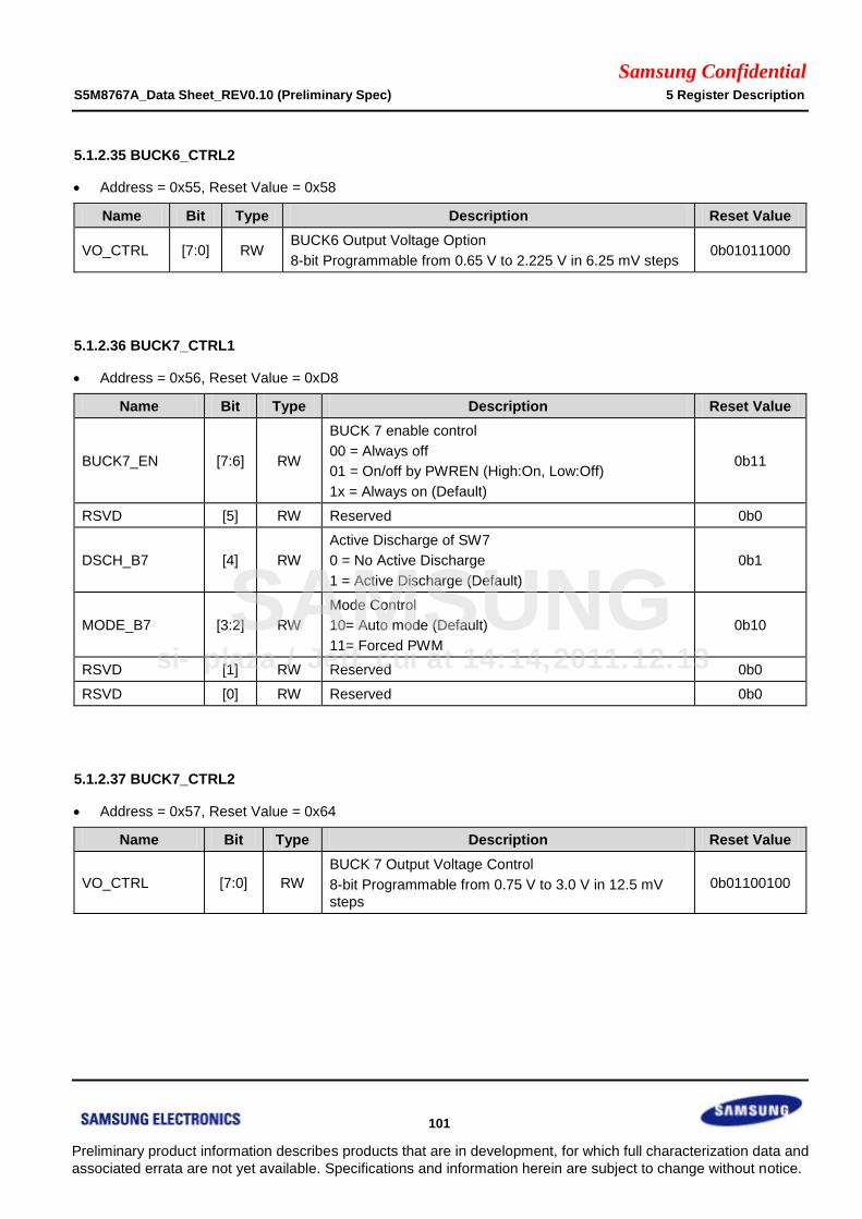
Samsung Confidential S5M8767A_Data Sheet_REV0.10 (Preliminary Spec) 5 Register Description
101
Preliminary product information describes products that are in development, for which full characterization data and
associated errata are not yet available. Specifications and information herein are subject to change without notice.
5.1.2.35 BUCK6_CTRL2
Address = 0x55, Reset Value = 0x58
Name Bit Type Description Reset Value
VO_CTRL [7:0] RW BUCK6 Output Voltage Option
8-bit Programmable from 0.65 V to 2.225 V in 6.25 mV steps 0b01011000
5.1.2.36 BUCK7_CTRL1
Address = 0x56, Reset Value = 0xD8
Name Bit Type Description Reset Value
BUCK7_EN [7:6] RW
BUCK 7 enable control
00 = Always off
01 = On/off by PWREN (High:On, Low:Off)
1x = Always on (Default)
0b11
RSVD [5] RW Reserved 0b0
DSCH_B7 [4] RW
Active Discharge of SW7
0 = No Active Discharge
1 = Active Discharge (Default)
0b1
MODE_B7 [3:2] RW
Mode Control
10= Auto mode (Default)
11= Forced PWM
0b10
RSVD [1] RW Reserved 0b0
RSVD [0] RW Reserved 0b0
5.1.2.37 BUCK7_CTRL2
Address = 0x57, Reset Value = 0x64
Name Bit Type Description Reset Value
VO_CTRL [7:0] RW
BUCK 7 Output Voltage Control
8-bit Programmable from 0.75 V to 3.0 V in 12.5 mV
steps
0b01100100
si-plaza / Jeff_cui at 14:14,2011.12.13
SAMSUNG

Samsung Confidential S5M8767A_Data Sheet_REV0.10 (Preliminary Spec) 5 Register Description
102
Preliminary product information describes products that are in development, for which full characterization data and
associated errata are not yet available. Specifications and information herein are subject to change without notice.
5.1.2.38 BUCK8_CTRL1
Address = 0x58, Reset Value = 0xD8
Name Bit Type Description Reset Value
BUCK8_EN [7:6] RW
BUCK8 enable control
00 = Always off
01 = On/off by PWREN (High: On, Low: Off)
1x = Always on (Default)
0b11
RSVD [5] RW Reserved 0b0
DSCH_B8 [4] RW
Active Discharge of SW8
0 = No Active Discharge
1 = Active Discharge (Default)
0b1
MODE_B8 [3:2] RW
Mode Control
10 = Auto mode (Default)
11 = Forced PWM
0b10
RSVD [1] RW Reserved 0b0
RSVD [0] RW Reserved 0b0
5.1.2.39 BUCK8_CTRL2
Address = 0x59, Reset Value = 0x34
Name Bit Type Description Reset Value
VO_CTRL [7:0] RW
BUCK 8 Output Voltage Control
8-bit Programmable from 0.75 V to 3.0V in 12.5 mV
steps
0b00110100
si-plaza / Jeff_cui at 14:14,2011.12.13
SAMSUNG
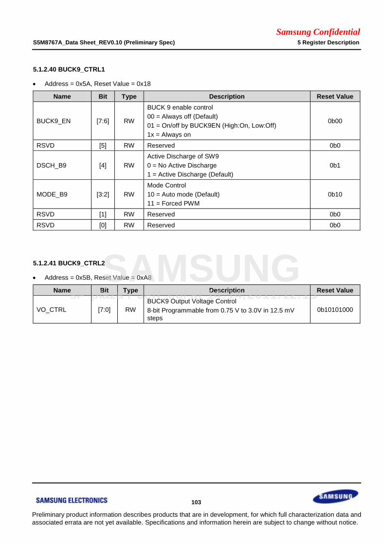
Samsung Confidential S5M8767A_Data Sheet_REV0.10 (Preliminary Spec) 5 Register Description
103
Preliminary product information describes products that are in development, for which full characterization data and
associated errata are not yet available. Specifications and information herein are subject to change without notice.
5.1.2.40 BUCK9_CTRL1
Address = 0x5A, Reset Value = 0x18
Name Bit Type Description Reset Value
BUCK9_EN [7:6] RW
BUCK 9 enable control
00 = Always off (Default)
01 = On/off by BUCK9EN (High:On, Low:Off)
1x = Always on
0b00
RSVD [5] RW Reserved 0b0
DSCH_B9 [4] RW
Active Discharge of SW9
0 = No Active Discharge
1 = Active Discharge (Default)
0b1
MODE_B9 [3:2] RW
Mode Control
10 = Auto mode (Default)
11 = Forced PWM
0b10
RSVD [1] RW Reserved 0b0
RSVD [0] RW Reserved 0b0
5.1.2.41 BUCK9_CTRL2
Address = 0x5B, Reset Value = 0xA8
Name Bit Type Description Reset Value
VO_CTRL [7:0] RW
BUCK9 Output Voltage Control
8-bit Programmable from 0.75 V to 3.0V in 12.5 mV
steps
0b10101000
si-plaza / Jeff_cui at 14:14,2011.12.13
SAMSUNG

Samsung Confidential S5M8767A_Data Sheet_REV0.10 (Preliminary Spec) 5 Register Description
104
Preliminary product information describes products that are in development, for which full characterization data and
associated errata are not yet available. Specifications and information herein are subject to change without notice.
Table 5 Voltage Table for BUCK 2/3/4
0x00 = 0.60000 0x20 = 0.80000 0x40 = 1.00000 0x60 = 1.20000 0x80 = 1.40000 0xA0 = 1.60000
0x01 = 0.60625 0x21 = 0.80625 0x41 = 1.00625 0x61 = 1.20625 0x81 = 1.40625
0x02 = 0.61250 0x22 = 0.81250 0x42 = 1.01250 0x62 = 1.21250 0x82 = 1.41250
0x03 = 0.61875 0x23 = 0.81875 0x43 = 1.01875 0x63 = 1.21875 0x83 = 1.41875
0x04 = 0.62500 0x24 = 0.82500 0x44 = 1.02500 0x64 = 1.22500 0x84 = 1.42500
0x05 = 0.63125 0x25 = 0.83125 0x45 = 1.03125 0x65 = 1.23125 0x85 = 1.43125
0x06 = 0.63750 0x26 = 0.83750 0x46 = 1.03750 0x66 = 1.23750 0x86 = 1.43750
0x07 = 0.64375 0x27 = 0.84375 0x47 = 1.04375 0x67 = 1.24375 0x87 = 1.44375
0x08 = 0.65000 0x28 = 0.85000 0x48 = 1.05000 0x68 = 1.25000 0x88 = 1.45000
0x09 = 0.65625 0x29 = 0.85625 0x49 = 1.05625 0x69 = 1.25625 0x89 = 1.45625
0x0A = 0.66250 0x2A = 0.86250 0x4A = 1.06250 0x6A = 1.26250 0x8A = 1.46250
0x0B = 0.66875 0x2B = 0.86875 0x4B = 1.06875 0x6B = 1.26875 0x8B = 1.46875
0x0C = 0.67500 0x2C = 0.87500 0x4C = 1.07500 0x6C = 1.27500 0x8C = 1.47500
0x0D = 0.68125 0x2D = 0.88125 0x4D = 1.08125 0x6D = 1.28125 0x8D = 1.48125
0x0E = 0.68750 0x2E = 0.88750 0x4E = 1.08750 0x6E = 1.28750 0x8E = 1.48750
0x0F = 0.69375 0x2F = 0.89375 0x4F = 1.09375 0x6F = 1.29375 0x8F = 1.49375
0x10 = 0.70000 0x30 = 0.90000 0x50 = 1.10000 0x70 = 1.30000 0x90 = 1.50000
0x11 = 0.70625 0x31 = 0.90625 0x51 = 1.10625 0x71 = 1.30625 0x91 = 1.50625
0x12 = 0.71250 0x32 = 0.91250 0x52 = 1.11250 0x72 = 1.31250 0x92 = 1.51250
0x13 = 0.71875 0x33 = 0.91875 0x53 = 1.11875 0x73 = 1.31875 0x93 = 1.51875
0x14 = 0.72500 0x34 = 0.92500 0x54 = 1.12500 0x74 = 1.32500 0x94 = 1.52500
0x15 = 0.73125 0x35 = 0.93125 0x55 = 1.13125 0x75 = 1.33125 0x95 = 1.53125
0x16 = 0.73750 0x36 = 0.93750 0x56 = 1.13750 0x76 = 1.33750 0x96 = 1.53750
0x17 = 0.74375 0x37 = 0.94375 0x57 = 1.14375 0x77 = 1.34375 0x97 = 1.54375
0x18 = 0.75000 0x38 = 0.95000 0x58 = 1.15000 0x78 = 1.35000 0x98 = 1.55000
0x19 = 0.75625 0x39 = 0.95625 0x59 = 1.15625 0x79 = 1.35625 0x99 = 1.55625
0x1A = 0.76250 0x3A = 0.96250 0x5A = 1.16250 0x7A = 1.36250 0x9A = 1.56250
0x1B = 0.76875 0x3B = 0.96875 0x5B = 1.16875 0x7B = 1.36875 0x9B = 1.56875
0x1C = 0.77500 0x3C = 0.97500 0x5C = 1.17500 0x7C = 1.37500 0x9C = 1.57500
0x1D = 0.78125 0x3D = 0.98125 0x5D = 1.18125 0x7D = 1.38125 0x9D = 1.58125
0x1E = 0.78750 0x3E = 0.98750 0x5E = 1.18750 0x7E = 1.38750 0x9E = 1.58750
0x1F = 0.79375 0x3F = 0.99375 0x5F = 1.19375 0x7F = 1.39375 0x9F = 1.59375
si-plaza / Jeff_cui at 14:14,2011.12.13
SAMSUNG

Samsung Confidential S5M8767A_Data Sheet_REV0.10 (Preliminary Spec) 5 Register Description
105
Preliminary product information describes products that are in development, for which full characterization data and
associated errata are not yet available. Specifications and information herein are subject to change without notice.
Table 6 Voltage Table for BUCK1/5/6
0x00= 0.65000 0x20 = 0.85000 0x40 = 1.05000 0x60 = 1.25000 0x80 = 1.45000 0xA0 = 1.65000 0xC0 = 1.85000 0xE0 = 2.05000
0x01 = 0.65625 0x21 = 0.85625 0x41 = 1.05625 0x61 = 1.25625 0x81 = 1.45625 0xA1 = 1.65625 0xC1 = 1.85625 0xE1 = 2.05625
0x02 = 0.66250 0x22 = 0.86250 0x42 = 1.06250 0x62 = 1.26250 0x82 = 1.46250 0xA2 = 1.66250 0xC2 = 1.86250 0xE2 = 2.06250
0x03 = 0.66875 0x23 = 0.86875 0x43 = 1.06875 0x63 = 1.26875 0x83 = 1.46875 0xA3 = 1.66875 0xC3 = 1.86875 0xE3 = 2.06875
0x04 = 0.67500 0x24 = 0.87500 0x44 = 1.07500 0x64 = 1.27500 0x84 = 1.47500 0xA4 = 1.67500 0xC4 = 1.87500 0xE4 = 2.07500
0x05 = 0.68125 0x25 = 0.88125 0x45 = 1.08125 0x65 = 1.28125 0x85 = 1.48125 0xA5 = 1.68125 0xC5 = 1.88125 0xE5 = 2.08125
0x06 = 0.68750 0x26 = 0.88750 0x46 = 1.08750 0x66 = 1.28750 0x86 = 1.48750 0xA6 = 1.68750 0xC6 = 1.88750 0xE6 = 2.08750
0x07 = 0.69375 0x27 = 0.89375 0x47 = 1.09375 0x67 = 1.29375 0x87 = 1.49375 0xA7 = 1.69375 0xC7 = 1.89375 0xE7 = 2.09375
0x08 = 0.70000 0x28 = 0.90000 0x48 = 1.10000 0x68 = 1.30000 0x88 = 1.50000 0xA8 = 1.70000 0xC8 = 1.90000 0xE8 = 2.10000
0x09 = 0.70625 0x29 = 0.90625 0x49 = 1.10625 0x69 = 1.30625 0x89 = 1.50625 0xA9 = 1.70625 0xC9 = 1.90625 0xE9 = 2.10625
0x0A = 0.71250 0x2A = 0.91250 0x4A = 1.11250 0x6A = 1.31250 0x8A = 1.51250 0xAA = 1.71250 0xCA = 1.91250 0xEA = 2.11250
0x0B = 0.71875 0x2B = 0.91875 0x4B = 1.11875 0x6B = 1.31875 0x8B = 1.51875 0xAB = 1.71875 0xCB = 1.91875 0xEB = 2.11875
0x0C = 0.72500 0x2C = 0.92500 0x4C = 1.12500 0x6C = 1.32500 0x8C = 1.52500 0xAC = 1.72500 0xCC = 1.92500 0xEC = 2.12500
0x0D = 0.73125 0x2D = 0.93125 0x4D = 1.13125 0x6D = 1.33125 0x8D = 1.53125 0xAD = 1.73125 0xCD = 1.93125 0xED = 2.13125
0x0E = 0.73750 0x2E = 0.93750 0x4E = 1.13750 0x6E = 1.33750 0x8E = 1.53750 0xAE = 1.73750 0xCE = 1.93750 0xEE = 2.13750
0x0F = 0.74375 0x2F = 0.94375 0x4F = 1.14375 0x6F = 1.34375 0x8F = 1.54375 0xAF = 1.74375 0xCF = 1.94375 0xEF = 2.14375
0x10 = 0.75000 0x30 = 0.95000 0x50 = 1.15000 0x70 = 1.35000 0x90 = 1.55000 0xB0 = 1.75000 0xD0 = 1.95000 0xF0 = 2.15000
0x11 = 0.75625 0x31 = 0.95625 0x51 = 1.15625 0x71 = 1.35625 0x91 = 1.55625 0xB1 = 1.75625 0xD1 = 1.95625 0xF1 = 2.15625
0x12 = 0.76250 0x32 = 0.96250 0x52 = 1.16250 0x72 = 1.36250 0x92 = 1.56250 0xB2 = 1.76250 0xD2 = 1.96250 0xF2 = 2.16250
0x13 = 0.76875 0x33 = 0.96875 0x53 = 1.16875 0x73 = 1.36875 0x93 = 1.56875 0xB3 = 1.76875 0xD3 = 1.96875 0xF3 = 2.16875
0x14 = 0.77500 0x34 = 0.97500 0x54 = 1.17500 0x74 = 1.37500 0x94 = 1.57500 0xB4 = 1.77500 0xD4 = 1.97500 0xF4 = 2.17500
0x15 = 0.78125 0x35 = 0.98125 0x55 = 1.18125 0x75 = 1.38125 0x95 = 1.58125 0xB5 = 1.78125 0xD5 = 1.98125 0xF5 = 2.18125
0x16 = 0.78750 0x36 = 0.98750 0x56 = 1.18750 0x76 = 1.38750 0x96 = 1.58750 0xB6 = 1.78750 0xD6 = 1.98750 0xF6 = 2.18750
0x17 = 0.79375 0x37 = 0.99375 0x57 = 1.19375 0x77 = 1.39375 0x97 = 1.59375 0xB7 = 1.79375 0xD7 = 1.99375 0xF7 = 2.19375
0x18 = 0.80000 0x38 = 1.0 0x58 = 1.2 0x78 = 1.40000 0x98 = 1.60000 0xB8 = 1.80000 0xD8 = 2.00000 0xF8 = 2.20000
0x19 = 0.80625 0x39 = 1.00625 0x59 = 1.20625 0x79 = 1.40625 0x99 = 1.60625 0xB9 = 1.80625 0xD9 = 2.00625 0xF9 = 2.20625
0x1A = 0.81250 0x3A = 1.01250 0x5A = 1.21250 0x7A = 1.41250 0x9A = 1.61250 0xBA = 1.81250 0xDA = 2.01250 0xFA = 2.21250
0x1B = 0.81875 0x3B = 1.01875 0x5B = 1.21875 0x7B = 1.41875 0x9B = 1.61875 0xBB = 1.81875 0xDB = 2.01875 0xFB = 2.21875
0x1C = 0.82500 0x3C = 1.02500 0x5C = 1.22500 0x7C = 1.42500 0x9C = 1.62500 0xBC = 1.82500 0xDC = 2.02500 0xFC = 2.22500
0x1D = 0.83125 0x3D = 1.03125 0x5D = 1.23125 0x7D = 1.43125 0x9D = 1.63125 0xBD = 1.83125 0xDD = 2.03125
0x1E = 0.83750 0x3E = 1.04750 0x5E = 1.23750 0x7E = 1.43750 0x9E = 1.63750 0xBE = 1.83750 0xDE = 2.03750
0x1F = 0.84375 0x3F = 1.04375 0x5F = 1.24375 0x7F = 1.44375 0x9F = 1.64375 0xBF = 1.84375 0xDF = 2.04375
si-plaza / Jeff_cui at 14:14,2011.12.13
SAMSUNG

Samsung Confidential S5M8767A_Data Sheet_REV0.10 (Preliminary Spec) 5 Register Description
106
Preliminary product information describes products that are in development, for which full characterization data and
associated errata are not yet available. Specifications and information herein are subject to change without notice.
Table 7 Voltage Table for BUCK7/8/9
0x00 = 0.7500 0x20 = 1.1500 0x40 = 1.5500 0x60 = 1.9500 0x80 = 2.3500 0xA0 = 2.7500
0x01 = 0.7625 0x21 = 1.1625 0x41 = 1.5625 0x61 = 1.9625 0x81 = 2.3625 0xA1 = 2.7625
0x02 = 0.7750 0x22 = 1.1750 0x42 = 1.5750 0x62 = 1.9750 0x82 = 2.3750 0xA2 = 2.7750
0x03 = 0.7875 0x23 = 1.1875 0x43 = 1.5875 0x63 = 1.9875 0x83 = 2.3875 0xA3 = 2.7875
0x04 = 0.8000 0x24 = 1.2000 0x44 = 1.6000 0x64 = 2.0000 0x84 = 2.4000 0xA4 = 2.8000
0x05 = 0.8125 0x25 = 1.2125 0x45 = 1.6125 0x65 = 2.0125 0x85 = 2.4125 0xA5 = 2.8125
0x06 = 0.8250 0x26 = 1.2250 0x46 = 1.6250 0x66 = 2.0250 0x86 = 2.4250 0xA6 = 2.8250
0x07 = 0.8375 0x27 = 1.2375 0x47 = 1.6375 0x67 = 2.0375 0x87 = 2.4375 0xA7 = 2.8375
0x08 = 0.8500 0x28 = 1.2500 0x48 = 1.6500 0x68 = 2.0500 0x88 = 2.4500 0xA8 = 2.85
0x09 = 0.8625 0x29 = 1.2625 0x49 = 1.6625 0x69 = 2.0625 0x89 = 2.4625 0xA9 = 2.8625
0x0A = 0.8750 0x2A = 1.2750 0x4A = 1.6750 0x6A = 2.0750 0x8A = 2.4750 0xAA = 2.8750
0x0B = 0.8875 0x2B = 1.2875 0x4B = 1.6875 0x6B = 2.0875 0x8B = 2.4875 0xAB = 2.8875
0x0C = 0.9000 0x2C = 1.3000 0x4C = 1.7000 0x6C = 2.1000 0x8C = 2.5000 0xAC = 2.9000
0x0D = 0.9125 0x2D = 1.3125 0x4D = 1.7125 0x6D = 2.1125 0x8D = 2.5125 0xAD = 2.9125
0x0E = 0.9250 0x2E = 1.3250 0x4E = 1.7250 0x6E = 2.1250 0x8E = 2.5250 0xAE = 2.9250
0x0F = 0.9375 0x2F = 1.3375 0x4F = 1.7375 0x6F = 2.1375 0x8F = 2.5375 0xAF = 2.9375
0x10 = 0.9500 0x30 = 1.3500 0x50 = 1.7500 0x70 = 2.1500 0x90 = 2.5500 0xB0 = 2.9500
0x11 = 0.9625 0x31 = 1.3625 0x51 = 1.7625 0x71 = 2.1625 0x91 = 2.5625 0xB1 = 2.9625
0x12 = 0.9750 0x32 = 1.3750 0x52 = 1.7750 0x72 = 2.1750 0x92 = 2.5750 0xB2 = 2.9750
0x13 = 0.9875 0x33 = 1.3875 0x53 = 1.7875 0x73 = 2.1875 0x93 = 2.5875 0xB3 = 2.9875
0x14 = 1.0000 0x34 = 1.4000 0x54 = 1.8000 0x74 = 2.2000 0x94 = 2.6000 0xB4 = 3.0000
0x15 = 1.0125 0x35 = 1.4125 0x55 = 1.8125 0x75 = 2.2125 0x95 = 2.6125
0x16 = 1.0250 0x36 = 1.4250 0x56 = 1.8250 0x76 = 2.2250 0x96 = 2.6250
0x17 = 1.0375 0x37 = 1.4375 0x57 = 1.8375 0x77 = 2.2375 0x97 = 2.6375
0x18 = 1.0500 0x38 = 1.4500 0x58 = 1.8500 0x78 = 2.2500 0x98 = 2.6500
0x19 = 1.0625 0x39 = 1.4625 0x59 = 1.8625 0x79 = 2.2625 0x99 = 2.6625
0x1A = 1.0750 0x3A = 1.4750 0x5A = 1.8750 0x7A = 2.2750 0x9A = 2.6750
0x1B = 1.0875 0x3B = 1.4875 0x5B = 1.8875 0x7B = 2.2875 0x9B = 2.6875
0x1C = 1.1000 0x3C = 1.5000 0x5C = 1.9000 0x7C = 2.3000 0x9C = 2.7000
0x1D = 1.1125 0x3D = 1.5125 0x5D = 1.9125 0x7D = 2.3125 0x9D = 2.7125
0x1E = 1.1250 0x3E = 1.5250 0x5E = 1.9250 0x7E = 2.3250 0x9E = 2.7250
0x1F = 1.1375 0x3F = 1.5375 0x5F = 1.9375 0x7F = 2.3375 0x9F = 2.7375
si-plaza / Jeff_cui at 14:14,2011.12.13
SAMSUNG
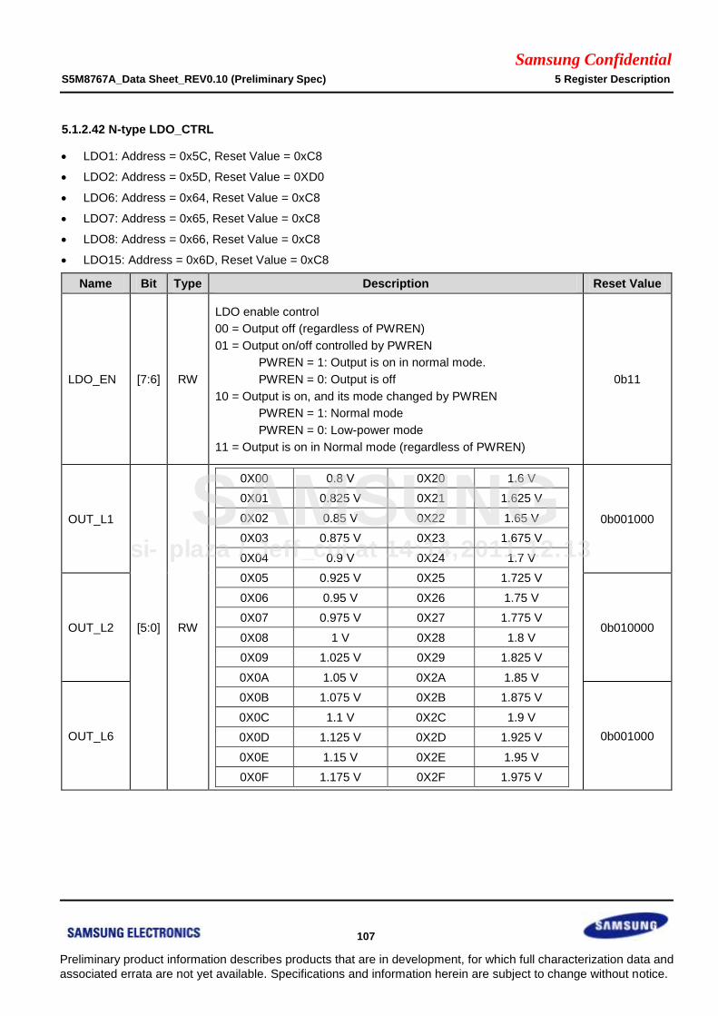
Samsung Confidential S5M8767A_Data Sheet_REV0.10 (Preliminary Spec) 5 Register Description
107
Preliminary product information describes products that are in development, for which full characterization data and
associated errata are not yet available. Specifications and information herein are subject to change without notice.
5.1.2.42 N-type LDO_CTRL
LDO1: Address = 0x5C, Reset Value = 0xC8
LDO2: Address = 0x5D, Reset Value = 0XD0
LDO6: Address = 0x64, Reset Value = 0xC8
LDO7: Address = 0x65, Reset Value = 0xC8
LDO8: Address = 0x66, Reset Value = 0xC8
LDO15: Address = 0x6D, Reset Value = 0xC8
Name Bit Type Description Reset Value
LDO_EN [7:6] RW
LDO enable control
00 = Output off (regardless of PWREN)
01 = Output on/off controlled by PWREN
PWREN = 1: Output is on in normal mode.
PWREN = 0: Output is off
10 = Output is on, and its mode changed by PWREN
PWREN = 1: Normal mode
PWREN = 0: Low-power mode
11 = Output is on in Normal mode (regardless of PWREN)
0b11
OUT_L1
[5:0] RW
0X00 0.8 V 0X20 1.6 V
0X01 0.825 V 0X21 1.625 V
0X02 0.85 V 0X22 1.65 V
0X03 0.875 V 0X23 1.675 V
0X04 0.9 V 0X24 1.7 V
0X05 0.925 V 0X25 1.725 V
0X06 0.95 V 0X26 1.75 V
0X07 0.975 V 0X27 1.775 V
0X08 1 V 0X28 1.8 V
0X09 1.025 V 0X29 1.825 V
0X0A 1.05 V 0X2A 1.85 V
0X0B 1.075 V 0X2B 1.875 V
0X0C 1.1 V 0X2C 1.9 V
0X0D 1.125 V 0X2D 1.925 V
0X0E 1.15 V 0X2E 1.95 V
0X0F 1.175 V 0X2F 1.975 V
0b001000
OUT_L2 0b010000
OUT_L6 0b001000
si-plaza / Jeff_cui at 14:14,2011.12.13
SAMSUNG
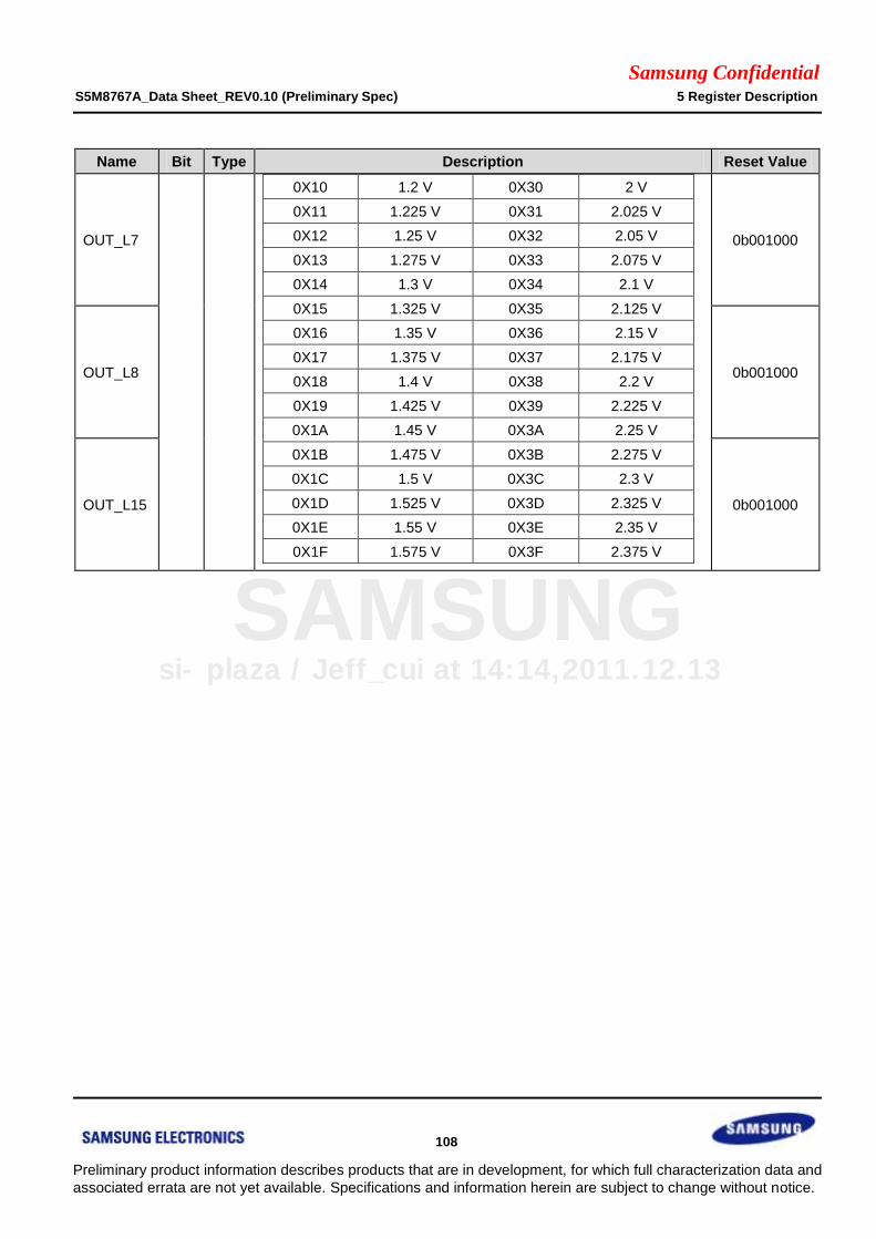
Samsung Confidential S5M8767A_Data Sheet_REV0.10 (Preliminary Spec) 5 Register Description
108
Preliminary product information describes products that are in development, for which full characterization data and
associated errata are not yet available. Specifications and information herein are subject to change without notice.
Name Bit Type Description Reset Value
OUT_L7
0X10 1.2 V 0X30 2 V
0X11 1.225 V 0X31 2.025 V
0X12 1.25 V 0X32 2.05 V
0X13 1.275 V 0X33 2.075 V
0X14 1.3 V 0X34 2.1 V
0X15 1.325 V 0X35 2.125 V
0X16 1.35 V 0X36 2.15 V
0X17 1.375 V 0X37 2.175 V
0X18 1.4 V 0X38 2.2 V
0X19 1.425 V 0X39 2.225 V
0X1A 1.45 V 0X3A 2.25 V
0X1B 1.475 V 0X3B 2.275 V
0X1C 1.5 V 0X3C 2.3 V
0X1D 1.525 V 0X3D 2.325 V
0X1E 1.55 V 0X3E 2.35 V
0X1F 1.575 V 0X3F 2.375 V
0b001000
OUT_L8 0b001000
OUT_L15 0b001000
si-plaza / Jeff_cui at 14:14,2011.12.13
SAMSUNG

Samsung Confidential S5M8767A_Data Sheet_REV0.10 (Preliminary Spec) 5 Register Description
109
Preliminary product information describes products that are in development, for which full characterization data and
associated errata are not yet available. Specifications and information herein are subject to change without notice.
5.1.2.43 P-type LDO_CTRL
LDO3: Address = 0x61, Reset Value = 0xD4
LDO4: Address = 0x62, Reset Value = 0xD4
LDO5: Address = 0x63, Reset Value = 0xD4
LDO9: Address = 0x67, Reset Value = 0x2C
LDO10: Address = 0x68, Reset Value = 0xD4
LDO11: Address = 0x69, Reset Value = 0xD4
LDO12: Address = 0x6A, Reset Value = 0xEC
LDO13: Address = 0x6B, Reset Value = 0xD4
LDO14: Address = 0x6C, Reset Value = 0xD4
LDO16: Address = 0x6E, Reset Value = 0xD4
LDO17: Address = 0x6F, Reset Value = 0xE8
LDO18: Address = 0x70, Reset Value = 0x28
LDO19: Address = 0x71, Reset Value = 0x2C
LDO20: Address = 0x72, Reset Value = 0x2C
LDO21: Address = 0x73, Reset Value = 0x2C
LDO22: Address = 0x74, Reset Value = 0x32
LDO23: Address = 0x75, Reset Value = 0x28
LDO24: Address = 0x76, Reset Value = 0x2C
LDO25: Address = 0x77, Reset Value = 0x08
LDO26: Address = 0x78, Reset Value = 0x14
LDO27: Address = 0x79, Reset Value = 0x14
LDO28: Address = 0x7A, Reset Value = 0x14
Name Bit Type Description Reset Value
LDO_EN [7:6] RW
LDO enable control: LDO5, LDO9, LDO10, LDO11, LDO12,
LDO13, LDO14, LDO16, LDO17, LDO19, LDO20, LDO21,
LDO22, LDO24, LDO25, LDO26, LDO27, LDO28,
►00 = Output off (regardless of PWREN)
►01 = Output on/off controlled by PWREN
PWREN = 1: Output is on in normal mode.
PWREN = 0: Output is off
►10 = Output is on, and its mode changed by PWREN
PWREN = 1: Normal mode
PWREN = 0: Low-power mode
►11 = Output is on in Normal mode (regardless of PWREN)
0b00:
LDO9,
LDO19,
LDO20,
LDO21,
LDO22,
LDO24,
LDO25,
LDO26,
LDO27,
LDO28
0b11:
LDO5,
LDO10,
si-plaza / Jeff_cui at 14:14,2011.12.13
SAMSUNG
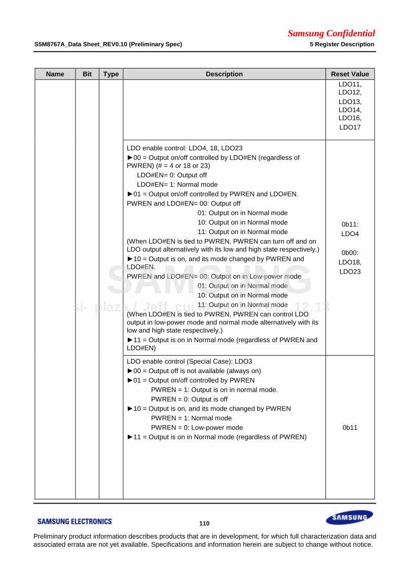
Samsung Confidential S5M8767A_Data Sheet_REV0.10 (Preliminary Spec) 5 Register Description
110
Preliminary product information describes products that are in development, for which full characterization data and
associated errata are not yet available. Specifications and information herein are subject to change without notice.
Name Bit Type Description Reset Value
LDO11,
LDO12,
LDO13,
LDO14,
LDO16,
LDO17
LDO enable control: LDO4, 18, LDO23
►00 = Output on/off controlled by LDO#EN (regardless of
PWREN) (# = 4 or 18 or 23)
LDO#EN= 0: Output off
LDO#EN= 1: Normal mode
►01 = Output on/off controlled by PWREN and LDO#EN.
PWREN and LDO#EN= 00: Output off
01: Output on in Normal mode
10: Output on in Normal mode
11: Output on in Normal mode
(When LDO#EN is tied to PWREN, PWREN can turn off and on
LDO output alternatively with its low and high state respectively.)
►10 = Output is on, and its mode changed by PWREN and
LDO#EN.
PWREN and LDO#EN= 00: Output on in Low-power mode
01: Output on in Normal mode
10: Output on in Normal mode
11: Output on in Normal mode
(When LDO#EN is tied to PWREN, PWREN can control LDO
output in low-power mode and normal mode alternatively with its
low and high state respectively.)
►11 = Output is on in Normal mode (regardless of PWREN and
LDO#EN)
0b11:
LDO4
0b00:
LDO18,
LDO23
LDO enable control (Special Case): LDO3
►00 = Output off is not available (always on)
►01 = Output on/off controlled by PWREN
PWREN = 1: Output is on in normal mode.
PWREN = 0: Output is off
►10 = Output is on, and its mode changed by PWREN
PWREN = 1: Normal mode
PWREN = 0: Low-power mode
►11 = Output is on in Normal mode (regardless of PWREN)
0b11
si-plaza / Jeff_cui at 14:14,2011.12.13
SAMSUNG
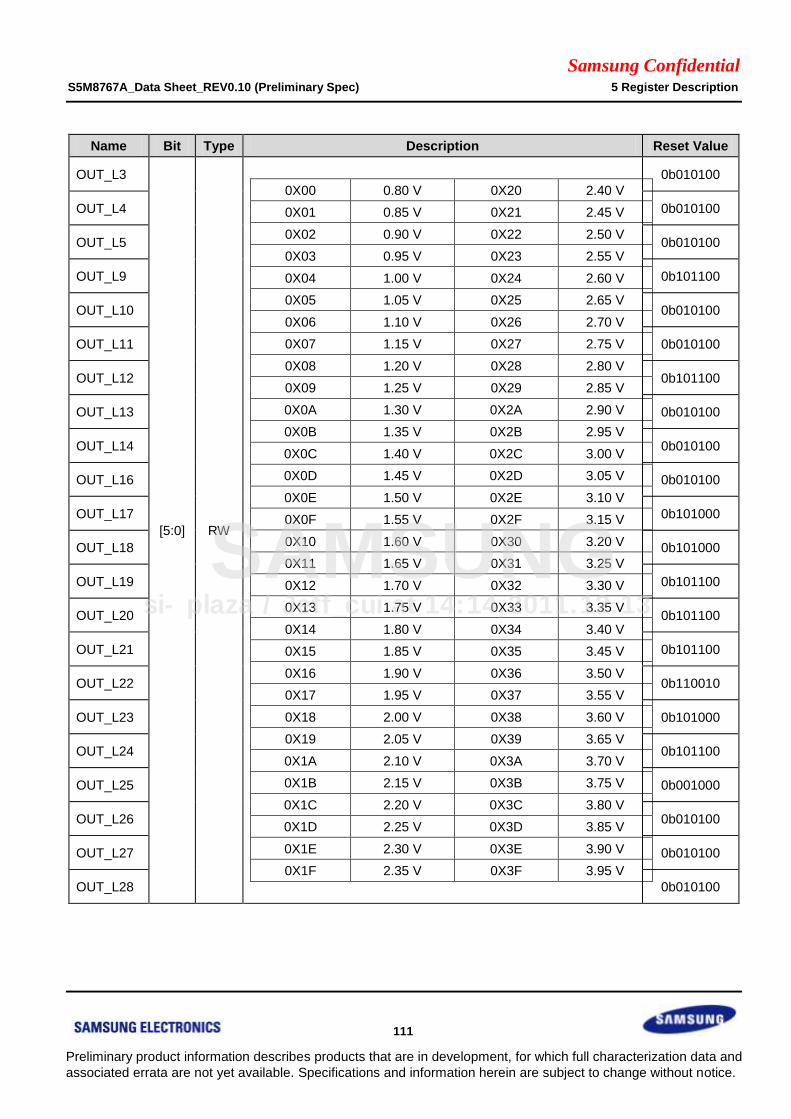
Samsung Confidential S5M8767A_Data Sheet_REV0.10 (Preliminary Spec) 5 Register Description
111
Preliminary product information describes products that are in development, for which full characterization data and
associated errata are not yet available. Specifications and information herein are subject to change without notice.
Name Bit Type Description Reset Value
OUT_L3
[5:0] RW
0X00 0.80 V 0X20 2.40 V
0X01 0.85 V 0X21 2.45 V
0X02 0.90 V 0X22 2.50 V
0X03 0.95 V 0X23 2.55 V
0X04 1.00 V 0X24 2.60 V
0X05 1.05 V 0X25 2.65 V
0X06 1.10 V 0X26 2.70 V
0X07 1.15 V 0X27 2.75 V
0X08 1.20 V 0X28 2.80 V
0X09 1.25 V 0X29 2.85 V
0X0A 1.30 V 0X2A 2.90 V
0X0B 1.35 V 0X2B 2.95 V
0X0C 1.40 V 0X2C 3.00 V
0X0D 1.45 V 0X2D 3.05 V
0X0E 1.50 V 0X2E 3.10 V
0X0F 1.55 V 0X2F 3.15 V
0X10 1.60 V 0X30 3.20 V
0X11 1.65 V 0X31 3.25 V
0X12 1.70 V 0X32 3.30 V
0X13 1.75 V 0X33 3.35 V
0X14 1.80 V 0X34 3.40 V
0X15 1.85 V 0X35 3.45 V
0X16 1.90 V 0X36 3.50 V
0X17 1.95 V 0X37 3.55 V
0X18 2.00 V 0X38 3.60 V
0X19 2.05 V 0X39 3.65 V
0X1A 2.10 V 0X3A 3.70 V
0X1B 2.15 V 0X3B 3.75 V
0X1C 2.20 V 0X3C 3.80 V
0X1D 2.25 V 0X3D 3.85 V
0X1E 2.30 V 0X3E 3.90 V
0X1F 2.35 V 0X3F 3.95 V
0b010100
OUT_L4 0b010100
OUT_L5 0b010100
OUT_L9 0b101100
OUT_L10 0b010100
OUT_L11 0b010100
OUT_L12 0b101100
OUT_L13 0b010100
OUT_L14 0b010100
OUT_L16 0b010100
OUT_L17 0b101000
OUT_L18 0b101000
OUT_L19 0b101100
OUT_L20 0b101100
OUT_L21 0b101100
OUT_L22 0b110010
OUT_L23 0b101000
OUT_L24 0b101100
OUT_L25 0b001000
OUT_L26 0b010100
OUT_L27 0b010100
OUT_L28 0b010100
si-plaza / Jeff_cui at 14:14,2011.12.13
SAMSUNG
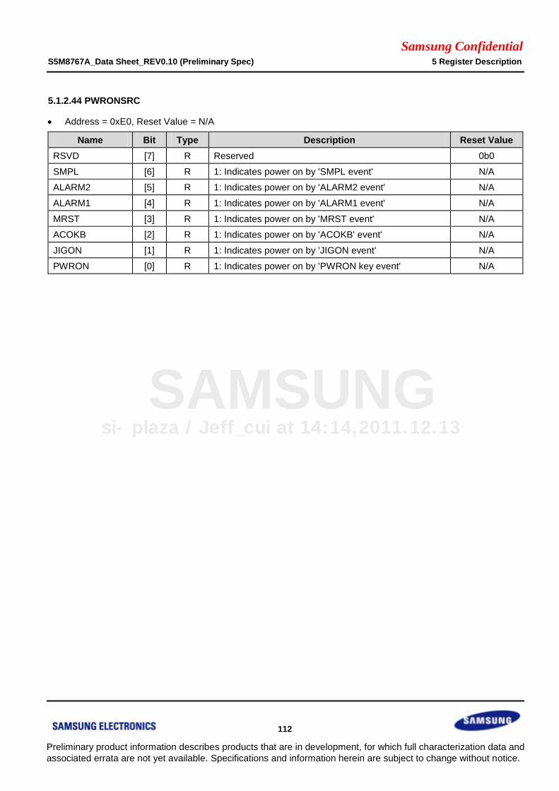
Samsung Confidential S5M8767A_Data Sheet_REV0.10 (Preliminary Spec) 5 Register Description
112
Preliminary product information describes products that are in development, for which full characterization data and
associated errata are not yet available. Specifications and information herein are subject to change without notice.
5.1.2.44 PWRONSRC
Address = 0xE0, Reset Value = N/A
Name Bit Type Description Reset Value
RSVD [7] R Reserved 0b0
SMPL [6] R 1: Indicates power on by 'SMPL event' N/A
ALARM2 [5] R 1: Indicates power on by 'ALARM2 event' N/A
ALARM1 [4] R 1: Indicates power on by 'ALARM1 event' N/A
MRST [3] R 1: Indicates power on by 'MRST event' N/A
ACOKB [2] R 1: Indicates power on by 'ACOKB' event' N/A
JIGON [1] R 1: Indicates power on by 'JIGON event' N/A
PWRON [0] R 1: Indicates power on by 'PWRON key event' N/A
si-plaza / Jeff_cui at 14:14,2011.12.13
SAMSUNG

Samsung Confidential S5M8767A_Data Sheet_REV0.10 (Preliminary Spec) 5 Register Description
113
Preliminary product information describes products that are in development, for which full characterization data and
associated errata are not yet available. Specifications and information herein are subject to change without notice.
5.2 RTC
5.2.1 Register Map Summary
Register Address Description Reset Value
SEC_TK 0x00 Current Seconds Set Register 0x00
MIN_TK 0x01 Current Minutes Set Register 0x00
HR_TK 0x02 Current Hours Set Register 0x00
WD_TK 0x03 Current Weeks Set Register 0x01
DATE_TK 0x04 Current Date Set Register 0x01
MON_TK 0x05 Current Month Set Register 0x01
YEAR_TK 0x06 Current Year Set Register 0x00
CENT_TK (BCD) 0x07 Current Century Set Register 0x00
SEC_Alarm0 0x08 Alarm0 Seconds Set Register 0x00
MIN_Alarm0 0X09 Alarm0 Minutes Set Register 0x00
HR_Alarm0 0x0A Alarm0 Hours Set Register 0x00
WD_Alarm0 0x0B Alarm0 Weeks Set Register 0x00
DATE_Alarm0 0x0C Alarm0 Date Set Register 0x01
MON_Alarm0 0x0D Alarm0 Month Set Register 0x00
YR_Alarm0 0x0E Alarm0 Year Set Register 0x00
CENT_Alarm0 (BCD) 0x0F Alarm0 Century Set Register 0x00
SEC_Alarm1 0x10 Alarm1 Seconds Set Register 0x00
MIN_Alarm1 0x11 Alarm1 Minutes Set Register 0x00
HR_Alarm1 0x12 Alarm1 Hours Set Register 0x00
WD_Alarm1 0x13 Alarm1 Weeks Set Register 0x00
DATE_Alarm1 0x14 Alarm1 Date Set Register 0x01
MON_Alarm1 0x15 Alarm1 Month Set Register 0x00
YR_Alarm1 0x16 Alarm1 Year Set Register 0x00
CENT_Alarm1 (BCD) 0x17 Alarm1 Century Set Register 0x00
RTC_CTRLM 0x18 RTC Control Mask Register 0x03
RTC_CTRL 0x19 RTC Control Register 0x00
TEST_STATUS 0x1A Status Register NA
SMPL_WTSR 0x1B SMPL WTSR Register 0x00
TEST_CON 0x1C Update Register 0x00
si-plaza / Jeff_cui at 14:14,2011.12.13
SAMSUNG

Samsung Confidential S5M8767A_Data Sheet_REV0.10 (Preliminary Spec) 5 Register Description
114
Preliminary product information describes products that are in development, for which full characterization data and
associated errata are not yet available. Specifications and information herein are subject to change without notice.
5.2.2 Bit Map Summary
Address Bit 7 Bit 6 Bit 5 Bit 4 Bit 3 Bit 2 Bit 1 Bit 0
0x00 RSVD SEC
0x01 RSVD MIN
0x02 RSVD AM/PM HOUR
0x03 RSVD SAT FRI THU WED TUE MON SUN
0x04 RSVD RSVD DATE
0x05 RSVD RSVD RSVD MONTH
0x06 YEAR
0x07 1000YEAR : BCD format only 100YEAR : BCD format only
0x08 ALM0_EN ALM0_SEC
0x09 ALM0_EN ALM0_MIN
0x0A ALM0_EN AM/PM ALM0_HOUR
0x0B ALM0_EN SAT FRI THU WED TUE MON SUN
0x0C ALM0_EN RSVD ALM0_DATE
0x0D ALM0_EN RSVD RSVD ALM0_MONTH
0x0E ALM0_EN ALM0_YEAR
0x0F ALM0_1000YEAR ALM0_100YEAR
0x10 ALM1_EN ALM1_SEC
0x11 ALM1_EN ALM1_MIN
0x12 ALM1_EN AM/PM ALM1_HOUR
0x13 ALM1_EN SAT FRI THU WED TUE MON SUN
0x14 ALM1_EN RSVD ALM1_DATE
0x15 ALM1_EN RSVD RSVD ALM1_MONTH
0x16 ALM1_EN ALM1_YEAR
0x17 ALM1_1000YEAR ALM1_100YEAR
0x18 1 SECM ALM
CENTM RSVD RSVD RSVD RSVD
MODE24
_12nM BCDM
0x19 1 SEC ALM
CENT RSVD RSVD RSVD RSVD
MODE24
_12n BCD
0x1A RSVD LEAP_
OK RSVD RSVD RSVD ALARM1 ALARM0 UDF
0x1B SMPL WTSR WTSR_H_TIMER SMPL_TIMER WTSR_TIMER
0x1C UDR_T SEL_
OSC
TEST_
OSC TIMEN
SEC_
FREEZE RSVD UDR
si-plaza / Jeff_cui at 14:14,2011.12.13
SAMSUNG

Samsung Confidential S5M8767A_Data Sheet_REV0.10 (Preliminary Spec) 5 Register Description
115
Preliminary product information describes products that are in development, for which full characterization data and
associated errata are not yet available. Specifications and information herein are subject to change without notice.
5.2.2.1 SEC_TK
Address = 0x00, Reset Value = 0x00
Name Bit Type Description Reset Value
RSVD [7] RW Reserved 0b0
SEC [6:0] RW
BIN Format BCD Format
0 sec 000_0000 0h 000_0000 0h
59 sec 011_1011 3Bh 101_1001 59h
If setting value is bigger than 3Bh in BIN mode, it is
set to 3Bh.
BCD/BIN mode selection is referred to 0x18 and
0x19.
0b0000000
5.2.2.2 MIN_TK
Address = 0x01, Reset Value = 0x00
Name Bit Type Description Reset Value
RSVD [7] RW Reserved 0b0
MIN [6:0] RW
B N Format BCD Format
0 min 000_0000 0h 000_0000 0h
59 min 011_1011 3Bh 101_1001 59h
If setting vales is bigger than 3Bh in BIN mode, it is
set to 3Bh.
BCD/BIN mode selection is referred to 0x18 and
0x19.
0b0000000
si-plaza / Jeff_cui at 14:14,2011.12.13
SAMSUNG

Samsung Confidential S5M8767A_Data Sheet_REV0.10 (Preliminary Spec) 5 Register Description
116
Preliminary product information describes products that are in development, for which full characterization data and
associated errata are not yet available. Specifications and information herein are subject to change without notice.
5.2.2.3 HR_TK
Address = 0x02, Reset Value = 0x00
Name Bit Type Description Reset Value
RSVD [7] RW Reserved 0b0
AM/PM [6] RW Select AM/PM 0b0
HOUR [5:0} RW
Mode BIN Format BCD Format
12
Hour
00_0000 0h 00_0000 0h
00_1100 0Ch 01_0010 12h
24
Hour
00_0000 0h 00_0000 0h
01_0111 17h 10_0011 23h
If setting vales is bigger than 17h in BIN mode, it is
set to 17h.
BCD/BIN mode and 12/24 hour mode selection is
referred to 0x18 and 0x19.
0b000000
5.2.2.4 WD_TK
Address = 0x03, Reset Value = 0x01
Name Bit Type Description Reset Value
RSVD [7] RW Reserved 0b0
SAT [6] RW
Multi-setting is not supported.
0b0
FRI [5] RW 0b0
THU [4] RW 0b0
WED [3] RW 0b0
TUE [2] RW 0b0
MON [1] RW 0b0
SUN [0] RW 0b1
si-plaza / Jeff_cui at 14:14,2011.12.13
SAMSUNG
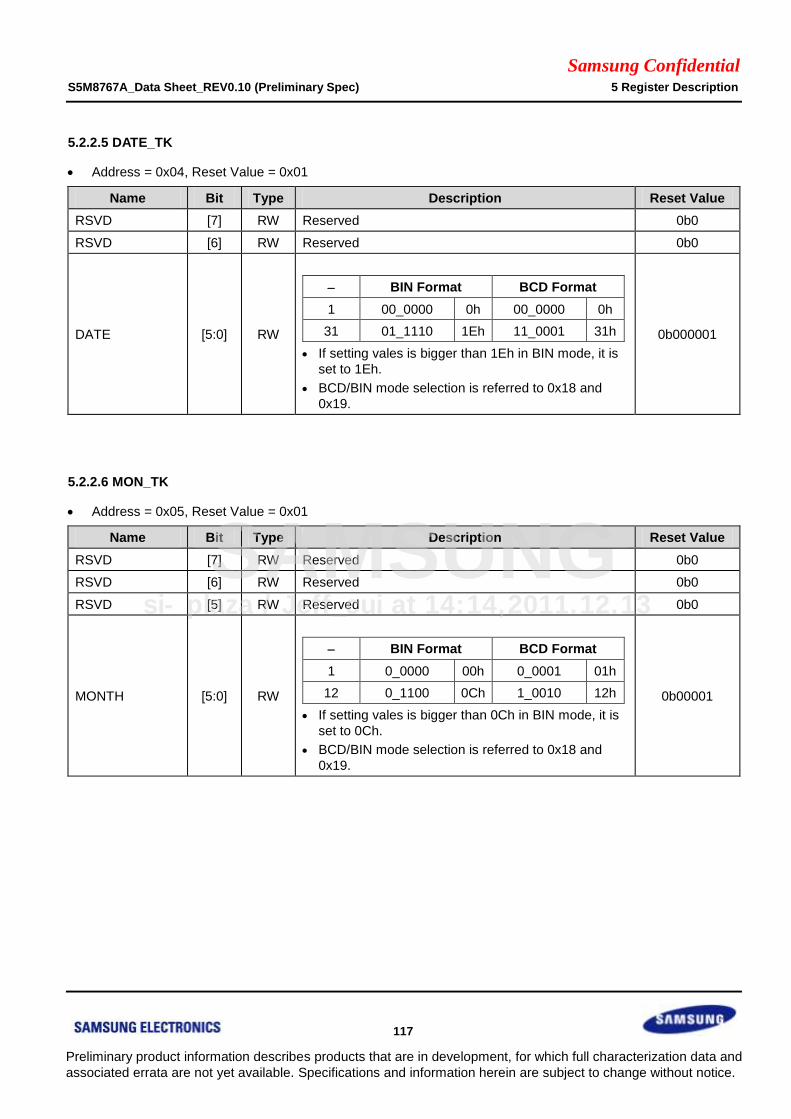
Samsung Confidential S5M8767A_Data Sheet_REV0.10 (Preliminary Spec) 5 Register Description
117
Preliminary product information describes products that are in development, for which full characterization data and
associated errata are not yet available. Specifications and information herein are subject to change without notice.
5.2.2.5 DATE_TK
Address = 0x04, Reset Value = 0x01
Name Bit Type Description Reset Value
RSVD [7] RW Reserved 0b0
RSVD [6] RW Reserved 0b0
DATE [5:0] RW
BIN Format BCD Format
1 00_0000 0h 00_0000 0h
31 01_1110 1Eh 11_0001 31h
If setting vales is bigger than 1Eh in BIN mode, it is
set to 1Eh.
BCD/BIN mode selection is referred to 0x18 and
0x19.
0b000001
5.2.2.6 MON_TK
Address = 0x05, Reset Value = 0x01
Name Bit Type Description Reset Value
RSVD [7] RW Reserved 0b0
RSVD [6] RW Reserved 0b0
RSVD [5] RW Reserved 0b0
MONTH [5:0] RW
BIN Format BCD Format
1 0_0000 00h 0_0001 01h
12 0_1100 0Ch 1_0010 12h
If setting vales is bigger than 0Ch in BIN mode, it is
set to 0Ch.
BCD/BIN mode selection is referred to 0x18 and
0x19.
0b00001
si-plaza / Jeff_cui at 14:14,2011.12.13
SAMSUNG

Samsung Confidential S5M8767A_Data Sheet_REV0.10 (Preliminary Spec) 5 Register Description
118
Preliminary product information describes products that are in development, for which full characterization data and
associated errata are not yet available. Specifications and information herein are subject to change without notice.
5.2.2.7 YEAR_TK
Address = 0x06, Reset Value = 0x00
Name Bit Type Description Reset Value
YEAR [7:0] RW
BIN Format BCD Format
1 0000_0000 00h 00 0_0000 00h
99 (BIN)
/79 (BCD) 0110_ 011 63h X111_1001 79h
Maximum setting value is 63h in BIN mode and 79h in BCD
mode.
0b00000000
5.2.2.8 CENT_TK (BC)
Address = 0x07, Reset Value = 0x00
Name Bit Type Description Reset Value
1000YEAR [7:4] RW
BIN Format BCD Format
1 X X 0000_0000 0h
9900 X X 1001_1001 99h
CENT is only valid in BCD mode.
0b0000
100YEAR [3:0] RW 0b0000
5.2.2.9 SEC_Alarm0
Address = 0x08, Reset Value = 0x00
Name Bit Type Description Reset Value
ALM0_EN [7] RW SEC ALARM enable 0b0
ALM0_SEC [6:0] RW
BIN Format BCD Format
0 sec 000_0000 0h 000_0000 0h
59 sec 011_1011 3Bh 101_1001 59h
0b0000000
si-plaza / Jeff_cui at 14:14,2011.12.13
SAMSUNG
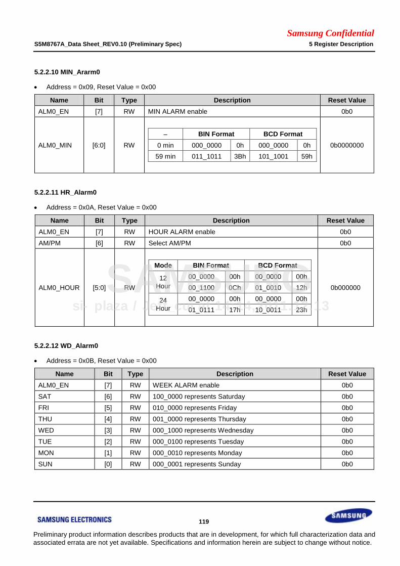
Samsung Confidential S5M8767A_Data Sheet_REV0.10 (Preliminary Spec) 5 Register Description
119
Preliminary product information describes products that are in development, for which full characterization data and
associated errata are not yet available. Specifications and information herein are subject to change without notice.
5.2.2.10 MIN_Ararm0
Address = 0x09, Reset Value = 0x00
Name Bit Type Description Reset Value
ALM0_EN [7] RW MIN ALARM enable 0b0
ALM0_MIN [6:0] RW
BIN Format BCD Format
0 min 000_0000 0h 000_0000 0h
59 min 011_1011 3Bh 101_1001 59h
0b0000000
5.2.2.11 HR_Alarm0
Address = 0x0A, Reset Value = 0x00
Name Bit Type Description Reset Value
ALM0_EN [7] RW HOUR ALARM enable 0b0
AM/PM [6] RW Select AM/PM 0b0
ALM0_HOUR [5:0] RW
Mode BIN Format BCD Format
12
Hour
00_0000 00h 00_0000 00h
00_1100 0Ch 01_0010 12h
24
Hour
00_0000 00h 00_0000 00h
01_0111 17h 10_0011 23h
0b000000
5.2.2.12 WD_Alarm0
Address = 0x0B, Reset Value = 0x00
Name Bit Type Description Reset Value
ALM0_EN [7] RW WEEK ALARM enable 0b0
SAT [6] RW 100_0000 represents Saturday 0b0
FRI [5] RW 010_0000 represents Friday 0b0
THU [4] RW 001_0000 represents Thursday 0b0
WED [3] RW 000_1000 represents Wednesday 0b0
TUE [2] RW 000_0100 represents Tuesday 0b0
MON [1] RW 000_0010 represents Monday 0b0
SUN [0] RW 000_0001 represents Sunday 0b0
si-plaza / Jeff_cui at 14:14,2011.12.13
SAMSUNG
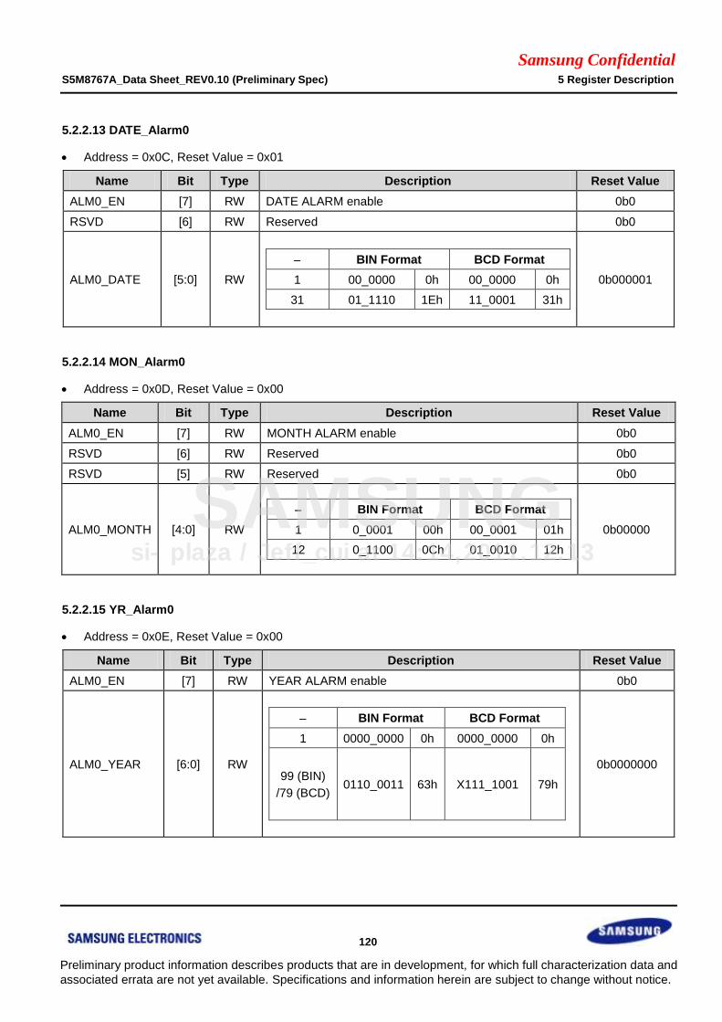
Samsung Confidential S5M8767A_Data Sheet_REV0.10 (Preliminary Spec) 5 Register Description
120
Preliminary product information describes products that are in development, for which full characterization data and
associated errata are not yet available. Specifications and information herein are subject to change without notice.
5.2.2.13 DATE_Alarm0
Address = 0x0C, Reset Value = 0x01
Name Bit Type Description Reset Value
ALM0_EN [7] RW DATE ALARM enable 0b0
RSVD [6] RW Reserved 0b0
ALM0_DATE [5:0] RW
BIN Format BCD Format
1 00_0000 0h 00_0000 0h
31 01_1110 1Eh 11_0001 31h
0b000001
5.2.2.14 MON_Alarm0
Address = 0x0D, Reset Value = 0x00
Name Bit Type Description Reset Value
ALM0_EN [7] RW MONTH ALARM enable 0b0
RSVD [6] RW Reserved 0b0
RSVD [5] RW Reserved 0b0
ALM0_MONTH [4:0] RW
BIN Format BCD Format
1 0_0001 00h 00_0001 01h
12 0_1100 0Ch 01_0010 12h
0b00000
5.2.2.15 YR_Alarm0
Address = 0x0E, Reset Value = 0x00
Name Bit Type Description Reset Value
ALM0_EN [7] RW YEAR ALARM enable 0b0
ALM0_YEAR [6:0] RW
BIN Format BCD Format
1 0000_0000 0h 0000_0000 0h
99 (BIN)
/79 (BCD) 0110_0011 63h X111_1001 79h
0b0000000
si-plaza / Jeff_cui at 14:14,2011.12.13
SAMSUNG

Samsung Confidential S5M8767A_Data Sheet_REV0.10 (Preliminary Spec) 5 Register Description
121
Preliminary product information describes products that are in development, for which full characterization data and
associated errata are not yet available. Specifications and information herein are subject to change without notice.
5.2.2.16 CENT_Alarm0
Address = 0x0F, Reset Value = 0x00
Name Bit Type Description Reset Value
ALM0_
1000YEAR [7:4] RW
BIN Format BCD Format
1 X X 0000_0000 0h
9900 X X 1001_1001 99h
If 0x0E[7] is set high, CENT ALARM enabled.
CENT is only valid in BCD mode.
CENT Comparison is activated when 0x19[6] is set to
high.
0b0000
ALM0_
100YEAR [3:0] RW 0b0000
5.2.2.17 SEC_Alarm1
Address = 0x10, Reset Value = 0x00
Name Bit Type Description Reset Value
ALM1_EN [7] RW SEC ALARM enable 0b0
ALM1_SEC [6:0] RW
BIN Format BCD Format
0 sec 000_0000 0h 000_0000 0h
59 sec 011_1011 3Bh 101_1001 59h
0b0000000
5.2.2.18 MIN_Alarm1
Address = 0x11, Reset Value = 0x00
Name Bit Type Description Reset Value
ALM1_EN [7] RW MIN ALARM enable 0b0
ALM1_MIN [6:0] RW
BIN Format BCD Format
0 min 000_0000 0h 000_0000 0h
59 min 011_1011 3Bh 101_1001 59h
0b0000000
si-plaza / Jeff_cui at 14:14,2011.12.13
SAMSUNG
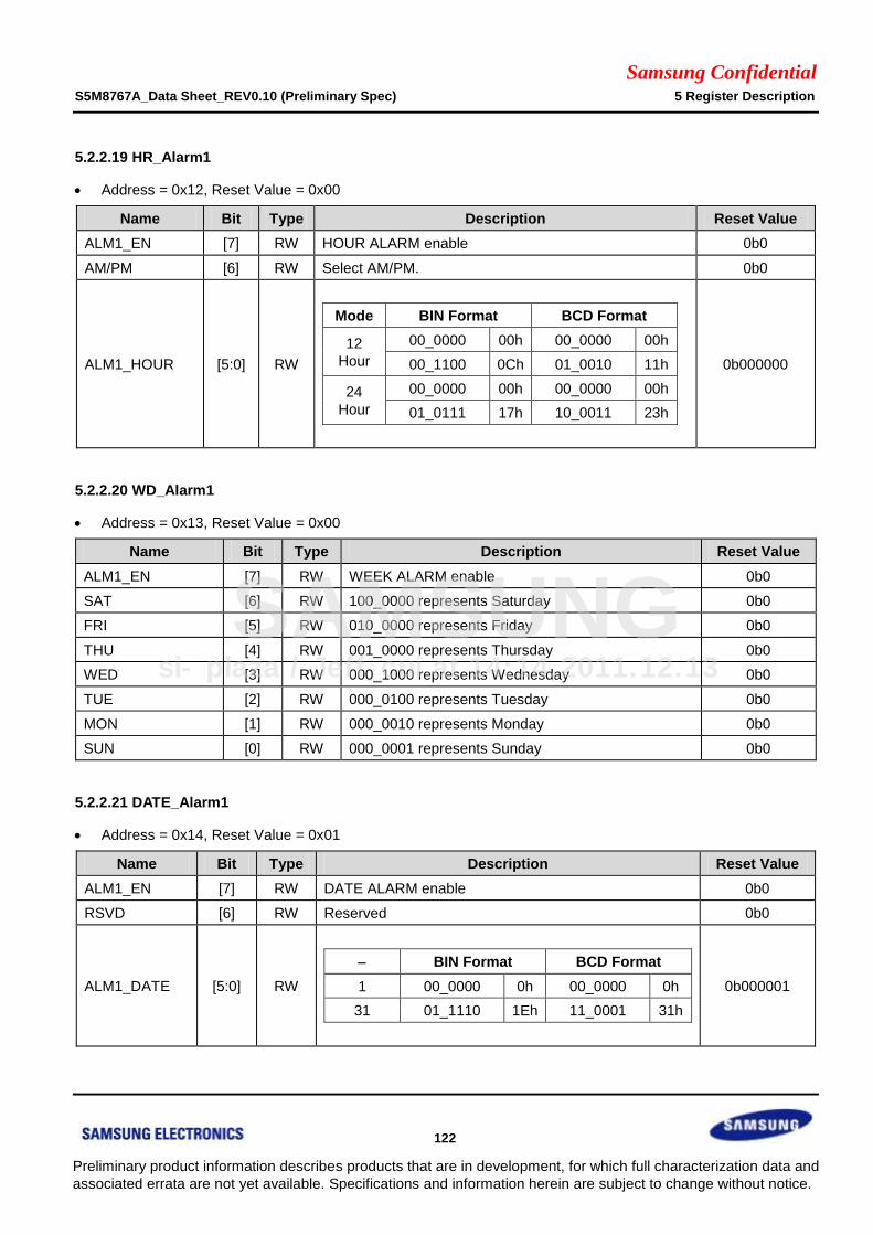
Samsung Confidential S5M8767A_Data Sheet_REV0.10 (Preliminary Spec) 5 Register Description
122
Preliminary product information describes products that are in development, for which full characterization data and
associated errata are not yet available. Specifications and information herein are subject to change without notice.
5.2.2.19 HR_Alarm1
Address = 0x12, Reset Value = 0x00
Name Bit Type Description Reset Value
ALM1_EN [7] RW HOUR ALARM enable 0b0
AM/PM [6] RW Select AM/PM. 0b0
ALM1_HOUR [5:0] RW
Mode BIN Format BCD Format
12
Hour
00_0000 00h 00_0000 00h
00_1100 0Ch 01_0010 11h
24
Hour
00_0000 00h 00_0000 00h
01_0111 17h 10_0011 23h
0b000000
5.2.2.20 WD_Alarm1
Address = 0x13, Reset Value = 0x00
Name Bit Type Description Reset Value
ALM1_EN [7] RW WEEK ALARM enable 0b0
SAT [6] RW 100_0000 represents Saturday 0b0
FRI [5] RW 010_0000 represents Friday 0b0
THU [4] RW 001_0000 represents Thursday 0b0
WED [3] RW 000_1000 represents Wednesday 0b0
TUE [2] RW 000_0100 represents Tuesday 0b0
MON [1] RW 000_0010 represents Monday 0b0
SUN [0] RW 000_0001 represents Sunday 0b0
5.2.2.21 DATE_Alarm1
Address = 0x14, Reset Value = 0x01
Name Bit Type Description Reset Value
ALM1_EN [7] RW DATE ALARM enable 0b0
RSVD [6] RW Reserved 0b0
ALM1_DATE [5:0] RW
BIN Format BCD Format
1 00_0000 0h 00_0000 0h
31 01_1110 1Eh 11_0001 31h
0b000001
si-plaza / Jeff_cui at 14:14,2011.12.13
SAMSUNG
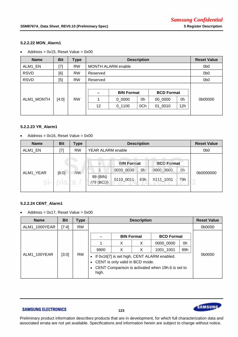
Samsung Confidential S5M8767A_Data Sheet_REV0.10 (Preliminary Spec) 5 Register Description
123
Preliminary product information describes products that are in development, for which full characterization data and
associated errata are not yet available. Specifications and information herein are subject to change without notice.
5.2.2.22 MON_Alarm1
Address = 0x15, Reset Value = 0x00
Name Bit Type Description Reset Value
ALM1_EN [7] RW MONTH ALARM enable 0b0
RSVD [6] RW Reserved 0b0
RSVD [5] RW Reserved 0b0
ALM1_MONTH [4:0] RW
BIN Format BCD Format
1 0_0000 0h 00_0000 0h
12 0_1100 0Ch 01_0010 12h
0b00000
5.2.2.23 YR_Alarm1
Address = 0x16, Reset Value = 0x00
Name Bit Type Description Reset Value
ALM1_EN [7] RW YEAR ALARM enable 0b0
ALM1_YEAR [6:0] RW
BIN Format BCD Format
1 0000_0000 0h 0000_0000 0h
99 (BIN)
/79 (BCD) 0110_0011 63h X111_1001 79h
0b0000000
5.2.2.24 CENT_Alarm1
Address = 0x17, Reset Value = 0x00
Name Bit Type Description Reset Value
ALM1_1000YEAR [7:4] RW
BIN Format BCD Format
1 X X 0000_0000 0h
9900 X X 1001_1001 99h
If 0x16[7] is set high, CENT ALARM enabled.
CENT is only valid in BCD mode.
CENT Comparison is activated when 19h.6 is set to
high.
0b0000
ALM1_100YEAR [3:0] RW 0b0000
si-plaza / Jeff_cui at 14:14,2011.12.13
SAMSUNG

Samsung Confidential S5M8767A_Data Sheet_REV0.10 (Preliminary Spec) 5 Register Description
124
Preliminary product information describes products that are in development, for which full characterization data and
associated errata are not yet available. Specifications and information herein are subject to change without notice.
5.2.2.25 RTL_CTRLM
Address = 0x18, Reset Value = 0x03
Name Bit Type Description Reset Value
1SECM [7] RW
Monitor selection.
0 = When read, ALARM0 status
1 = When read, 1SEC period
0b0
ALMCENTM [6] RW
ALMCENT
0 = Not masked
1 = Masked
0b0
RSVD [5] RW Reserved 0b0
RSVD [4] RW Reserved 0b0
RSVD [3] RW Reserved 0b0
RSVD [2] RW Reserved 0b0
MODE24_12nM [1] RW
Mode24_12n
0 = Not masked
1 = Masked
0b1
BCDM [0] RW
BCD
0 = Not masked
1 = Masked
0b1
5.2.2.26 RTL_CTRL
Address = 0x19, Reset Value = 0x00
Name Bit Type Description Reset Value
1SEC [7] RW
Monitor selection.
0 = When read, ALARM1 status
1 = When read, 1SEC period
0b0
ALMCENT [6] RW 0 = Only compare YEAR
1 = Compare both CENT and YEAR 0b0
RSVD [5] RW Reserved 0b0
RSVD [4] RW Reserved 0b0
RSVD [3] RW Reserved 0b0
RSVD [2] RW Reserved 0b0
MODE24_12n [1] RW 0 = 12 hour mode
1 = 24 hour mode 0b0
BCD [0] RW 0 = Binary mode
1 = BCD mode 0b0
si-plaza / Jeff_cui at 14:14,2011.12.13
SAMSUNG
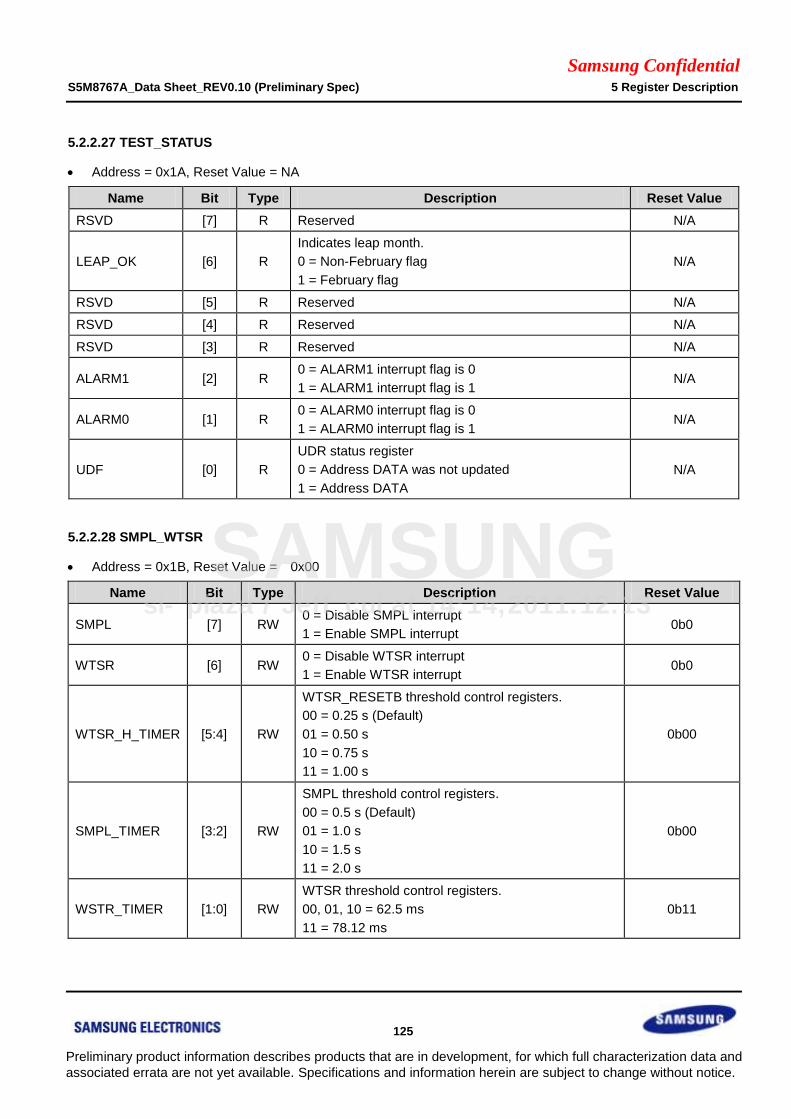
Samsung Confidential S5M8767A_Data Sheet_REV0.10 (Preliminary Spec) 5 Register Description
125
Preliminary product information describes products that are in development, for which full characterization data and
associated errata are not yet available. Specifications and information herein are subject to change without notice.
5.2.2.27 TEST_STATUS
Address = 0x1A, Reset Value = NA
Name Bit Type Description Reset Value
RSVD [7] R Reserved N/A
LEAP_OK [6] R
Indicates leap month.
0 = Non-February flag
1 = February flag
N/A
RSVD [5] R Reserved N/A
RSVD [4] R Reserved N/A
RSVD [3] R Reserved N/A
ALARM1 [2] R 0 = ALARM1 interrupt flag is 0
1 = ALARM1 interrupt flag is 1 N/A
ALARM0 [1] R 0 = ALARM0 interrupt flag is 0
1 = ALARM0 interrupt flag is 1 N/A
UDF [0] R
UDR status register
0 = Address DATA was not updated
1 = Address DATA
N/A
5.2.2.28 SMPL_WTSR
Address = 0x1B, Reset Value = 0x00
Name Bit Type Description Reset Value
SMPL [7] RW 0 = Disable SMPL interrupt
1 = Enable SMPL interrupt 0b0
WTSR [6] RW 0 = Disable WTSR interrupt
1 = Enable WTSR interrupt 0b0
WTSR_H_TIMER [5:4] RW
WTSR_RESETB threshold control registers.
00 = 0.25 s (Default)
01 = 0.50 s
10 = 0.75 s
11 = 1.00 s
0b00
SMPL_TIMER [3:2] RW
SMPL threshold control registers.
00 = 0.5 s (Default)
01 = 1.0 s
10 = 1.5 s
11 = 2.0 s
0b00
WSTR_TIMER [1:0] RW
WTSR threshold control registers.
00, 01, 10 = 62.5 ms
11 = 78.12 ms
0b11
si-plaza / Jeff_cui at 14:14,2011.12.13
SAMSUNG

Samsung Confidential S5M8767A_Data Sheet_REV0.10 (Preliminary Spec) 5 Register Description
126
Preliminary product information describes products that are in development, for which full characterization data and
associated errata are not yet available. Specifications and information herein are subject to change without notice.
5.2.2.29 TEST_CON
Address = 0x1C, Reset Value = 0x00
Name Bit Type Description Reset Value
UDR_T [7:6] RW
Determines UDR (Update Register) time.
00 = 7.32 ms (Default)
01 = 1.83 ms
10 = 3.66 ms
11 = 0.45 ms
0b00
SEL_OSC [5] RW 0 = SEC counter clock inversion off
1 = SEC counter clock inversion on 0b0
TEST_OSC [4] RW 0 = 1 Hz for SEC counter
1 = 16 Hz for SEC counter 0b0
TIMEN [3] RW Enable write current time register 0b0
SEC_FREEZE [2] RW
This bit freezes the RTC.
0 = Normal Timer
1 = Clock Disable for SEC Counter
0b0
RESERVED [1] RW Reserved 0b0
UDR [0] RW
Enable flag of update. UDR is auto cleared to after
the registers data have been transferred.
0 = Address & Data Hold
1 = Address & Data Update Enable
0b0
si-plaza / Jeff_cui at 14:14,2011.12.13
SAMSUNG
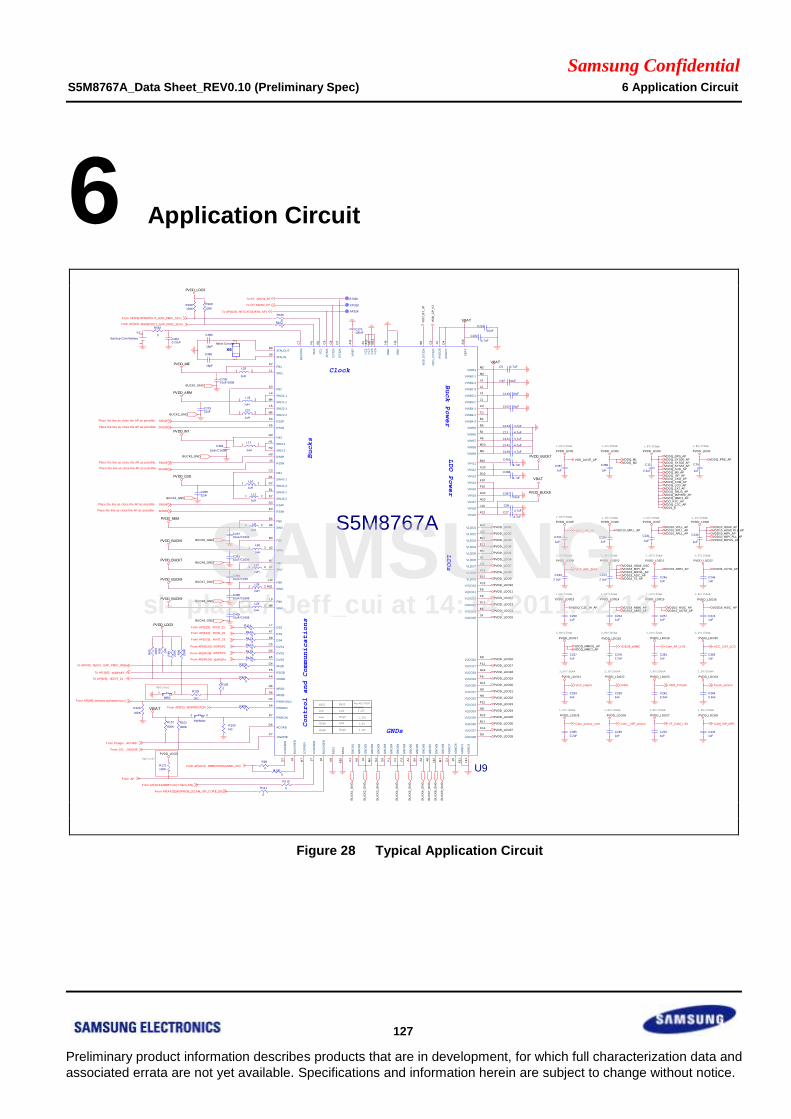
Samsung Confidential S5M8767A_Data Sheet_REV0.10 (Preliminary Spec) 6 Application Circuit
127
Preliminary product information describes products that are in development, for which full characterization data and
associated errata are not yet available. Specifications and information herein are subject to change without notice.
6 Application Circuit
Figure 28 Typical Application Circuit
R127
0
R1260
L25
1uH
1 2
VDDQ_MMC3_AP
PVDD_MIF
C23510uF/1608
XPWRRGTONFrom AP[P2]: R105
0
VDDQ_SYS33_AP
C386
18pF
VDD_RTC_AP
C388
18pF
L23
1uH
1 2
L24
1uH
1 2
PVDD_ARM
C22522uF
C250
1uF
L12
1uH
1 2
C254
1uF
C257
1uF
PVDD_LDO13 PVDD_LDO15PVDD_LDO14
3.0V/150mA1.8V/150mA1.8V/300mA
R120
200K
XPSHOLD(PWRHOLD)From AP[M5]:
PVDD_INT
C25522uF L11
1uH
1 2
L10
1uH
1 2
Control and Communications
LDOs
Bucks
GNDs
Buck Power
LDO Power
Clock
U9
S5M8767A
CP
32K
C8
XTALINA9
XTALOUTB9
AP
32K
C9
MR1BG5
RSOBF5
IRQBG4
VINB1M2
SW1L1
GN
DB
1K
1
FB1K2
PWRENE4
VINB2-1M3
SW21-1L4
GN
DB
2K
6
FB2K3
BK
CO
INC
7
PWRHOLDH4
JIGONBF7
PWRONE7
ONOBF4
ACOKBD6
VINL1B10
VLDO13D11
VLDO12F9
AG
ND
2L11
AG
ND
1K
11
VLDO23F12
VINL2C10
VLDO11E9
SC
LE
6
SD
AF
6
GN
DB
8L12
VLDO20G11
VLDO10C12
VLDO3B12
VLDO9E12
VLDO27C11
VLDO17F11
MR2BG6
VD
D_C
P32K
C6
VINL3D10
VINL4E10
VINL5F10
VINL6G10
VINL7H10
VLDO24G8
VLDO22H9
VINB3-2J1
GN
DB
3G
1
SW3-1H1
VINB2-2L3
SW21-2M4
SW22-1L5
SW22-2M5
GN
DB
2L6
VINB3-1J2
SW3-2H2
GN
DB
3G
2
FB3G3
GN
DB
4F
2
SW42-2E2
GN
DB
4F
1
SW41-2D2
SW42-1E1
VINB4-1C2
SW41-1D1
VINB4-2C1
FB4C3
SW5A5
GN
DB
5A
4
FB5B5
VINB5B6
GN
DB
5B
4
VINB6B1
SW6A2
FB6B3
GN
DB
6A
3
VINB7A6
VD
D_B
T32K
B8
SW7A7
FB7B7
GN
DB
7A
8
VINL8J10
VINB8M10
B5S
2K
10
VLDO15J9
VLDO25D12
VLDO28D9
VLDO14E8
VLDO19F8
VLDO16D8
VLDO26B11
VR
EF
A11
LD
O18E
NG
7
LD
O4E
NH
7
AV
DD
TD
4
AV
DD
BJ4
AG
ND
BJ5
AG
ND
TC
4
GN
DB
9M
7
BU
CK
9E
NL8
VINB9M9
FB9L9
B5S
1K
9
GN
DH
6
GN
DH
5
BU
CK
6E
NJ6
VB
AT
A10
VINB4-3B2
GN
DB
4F
3
VINB2-3L2
GN
DB
2M
6
SW9M8
DVS1C5
DVS2D5
DVS3E5
RS3PH3
RS3NJ3
RS2PK4
RS2NK5
RS4PD3
RS4NE3
FB8L10
SW8M11
DS2L7
DS3K7
DS4K8
VINL9K12
VLDO1H11
VLDO2J12
VLDO4E11
VLDO5H8
VLDO6J8
VLDO7J11
VLDO8H12
VLDO18G12
VLDO21G9
BT
32K
D7
NC
1A
1
NC
2A
12
NC
5M
1
NC
6M
12
LD
O23E
NJ7
VBAT
C381
1uF
C383
1uF
C378
2.2uF
C227
1uF
PVDD_LDO18
PVDD_LDO21
PVDD_LDO20PVDD_LDO19
PVDD_LDO25
PVDD_LDO24PVDD_LDO23PVDD_LDO22
PVDD_LDO17
C384
2.2uF
C239
1uF
C234
1uF
C242
2.2uF
C385
2.2uF
PVDD_LDO2
PVDD_LDO1
PVDD_LDO4
PVDD_LDO3
PVDD_G3D
C397
10uF
C398
4.7uF
PVDD_BUCK7
X6
Micro Cry stal
12
VBAT
C374
1uF
C23710uF/C1608
L8
1uH
1 2
PVDD_LDO16
PVDD_MEM
SNS3PPlace the line as close the AP as possible:
SNS2PPlace the line as close the AP as possible:
SNS4PPlace the line as close the AP as possible:
SNS3NPlace the line as close the AP as possible:
SNS2NPlace the line as close the AP as possible:
C39410uF/C108
SNS4NPlace the line as close the AP as possible:
PVDD_BUCK7
R56
14K
R101
800K
R122
800K
L26
1uH
1 2
C39110uF/C1608
VDDQ_C2C_W_AP
PVDD_BUCK6
R92
200K
L27
1uH
1 2
C373100nF
VDD18_ABB0_APVDD18_ABB2_AP
L28
1uH
1 2
PVDD_BUCK8
XnRESETTo AP:[N5]
VDDQ_PRE_AP
PVDD_LDO28
C433
1uF
C39510uF/C1608
C252
1uF
C249
1uF
1.8V/150mA1.8V/300mA1.0V/150mA
VDD10_UOTG_APVDD10_HSIC_AP VDD18_HSIC_AP
PVDD_LDO27PVDD_LDO26
1.8V/150mA
2.8V/300mA
1.8V/150mA 1.8V/150mA1.0V/150mA
2.8V/150mA 3.0V/150mA3.0V/150mA
L29
1uH
1 2
C40510uF/C1608
PVDD_BUCK9
C231
1uF
VBAT
R170
0
C232
4.7uF
C253
10uF
XMMC0CDN(eMMC_EN)From AP[AF4]:
R85
200K
R124
0
R99
200K
PVDD_LDO5
R123
0
VCC_I.8V_IO
XM0FCLE(T-f lash_EN)From AP[AD14]:
R110
0
PVDD_LDO3
R98
0
1.8V/150mA
Y2
Backup Coin Battery
12
C4030.22uF
R562
0
C236
1uF
XRTCXTI(32KHz_AP)To AP[AJ6]:
PVDD_LDO6
VDDQ_MMC01_APVDDQ_MMC2_AP
VDDQ_C2C_AP
VDD28_eMMC Cam_AF_3.0V VCC_3.0V_LCD
C12
2.2uF
APFrom
C27
4.7uF
C96
4.7uF
VDD10_MPLL_AP
1.0V/150mA
3.0V/300mA2.8V/300mA3.3V/300mA
R100
NC
1.8V/150mA1.8V/150mA1.8V/150mA
3.0V/150mA
1.2V/300mA
VCC_Haptic
C241
1uF
IRDA
XISPRGB_2(CAM_ISP_CORE_EN)From AP[AA25]):
VDD_T-Flash Touch_sensor
PVDD_LDO7
Cam_sensor_core
R128
0
Cam__ISP_sensor
R129
NC
VDD10_APLL_AP
VDD10_VPLL_APVDD10_EPLL_AP
Optional
PVDD_BUCK8
1.0V/150mA
C13 4.7uF
C5 4.7uF
C102 10uF
C97 10uF
C140 10uF
C139 4.7uF
C142 4.7uF
C141 4.7uF
C143 4.7uF
VT_CAM_1.8V
VBAT
CAM_ISP_MIPI
Low
B5S2B5S1
Low
LowHigh
HighLow
1.2V
Buck5/LDO2
Output
HighHigh 1.8V
1.5V
1.35V
BU
CK
1_G
ND
Optional
R172
100K
PVDD_LDO1
PVDD_LDO3
1.2V/450mA
PVDD_LDO2
MRB
21
BU
CK
3_G
ND
BU
CK
2_G
ND
BU
CK
5_G
ND
BU
CK
4_G
ND
BU
CK
7_G
ND
BU
CK
6_G
ND
BU
CK
8_G
ND
BU
CK
9_G
ND
PVDD_LDO18
PVDD_LDO16
PVDD_LDO17
PVDD_LDO20
PVDD_LDO19
BUCK1_GND
PWRON
21
BUCK2_GND
PVDD_LDO22
PVDD_LDO21
PVDD_LDO25
PVDD_LDO24
PVDD_LDO23
C382
10uF/C1608
PVDD_LDO28
PVDD_LDO27
PVDD_LDO26
BUCK3_GND
32KHz_CPTo CP:
32KHz_BTTo BT:
BUCK4_GND
CP32K
BT32K
AP32K
BUCK5_GND
BUCK6_GND
C240
1uF
PVDD_LDO8
1.0V/300mA
BUCK7_GND
BUCK8_GND
BUCK9_GND
VDD10_HDMI_APVDD10_HDMI_PLL_AP
VDD10_MIPI_PLL_APVDD10_MIPI2L_AP
VDD10_MIPI_AP
VD
D_C
P_IO
VD
D_B
T_IO
PVDD_LDO9
C243
2.2uF
VCC_MIC_BIAS
R111
0
XVVD_21From AP[E23]:
XISPGP3From AP[AF24]:
ACOKBFrom Chager :
C224
2.2uF
PVDD_LDO10
JIGONBFrom JIG :
3.0V/400mA
VDD18_MIPI_APVDD18_MIPI2L_AP
R109
100K
R108
100K
VDD18_HDMI_OSC
PVDD_LDO3
VDD18_TS_APVDD18_ADC_AP
PVDD_LDO3
XEINT_7(AP_PMIC_IRQ)To AP[V6]:
XEINT_23To AP[W3]:
VDD_ALIVE_APVDDQ_M2VDDQ_M1
C387
1uF
C389
1uF
VDDQ_GPS_APVDDQ_SYS00_AP
VDDQ_AUD_AP
PVDD_LDO14
PVDD_LDO12
PVDD_LDO13
PVDD_LDO15
PVDD_LDO11
PVDD_LDO5
PVDD_LDO6
PVDD_LDO7
PVDD_LDO8
PVDD_LDO9
PVDD_LDO10
PVDD_LDO4
VDDQ_M0_AP
C16
1uF
VDDQ_ISP_APVDDQ_CKO_AP
C245
1uF
PVDD_LDO11
VDDQ_SYS02_AP
VDD18_ABB1_AP
VDDQ_CAM_AP
C246
1uF
PVDD_LDO12
VDDQ_LCD_AP
C401
4.7uF
R106
0R107
0XPWMTOUT_2(AP_PMIC_SDA)From AP[D9]:
VDDQ_EXT_AP
XPWMTOUT_3(AP_PMIC_SCL)From AP[F9]:
VDD33_UOTG_AP
VDDQ_SBUS_AP
XVVD_23From AP[D25]:
XVVD_22From AP[F24]:
XISPGP2From AP[AD24]:
VDDQ_MIPIHSI_AP
XISPGP4From AP[AH24]:
R112
0R113
0
R114
0
VDD1_E
R125
0
si-plaza / Jeff_cui at 14:14,2011.12.13
SAMSUNG
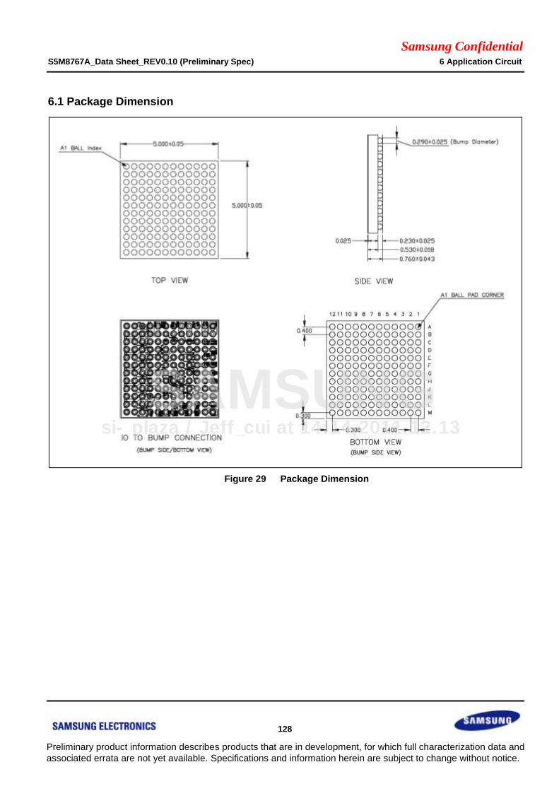
Samsung Confidential S5M8767A_Data Sheet_REV0.10 (Preliminary Spec) 6 Application Circuit
128
Preliminary product information describes products that are in development, for which full characterization data and
associated errata are not yet available. Specifications and information herein are subject to change without notice.
6.1 Package Dimension
Figure 29 Package Dimension
si-plaza / Jeff_cui at 14:14,2011.12.13
SAMSUNG