defects analysis and a self-repairable strategy for
TRANSCRIPT

Defects Analysis and
A Self-Repairable Strategy for
Tunable RF MEMS Filter
by
Ker Chia Lee
A thesis submitted for the degree of
Master of Engineering
at the
School of Engineering, Computing and Science
Swinburne University of Technology
Malaysia
2010

i
Abstract
Radio frequency (RF) Micro-Electro-Mechanical Systems (MEMS) is currently a developing
field. In order to make RF MEMS devices more applicable and marketable, the reliability and
testability of the device are critical.
In this thesis, a testing methodology to be applied onto the RF MEMS devices is proposed. The
RF MEMS device under test is the tunable filter with RF MEMS switches.
First, the layout of the tunable MEMS filter is determined. Then electromagnetic simulation is
carried out on the filter. Faults are introduced into the layouts of the filters and the frequency
output responses of the faulty filter are simulated using the Sonnet EM simulation software. The
faults that are simulated are broken structures, parametric variation, stuck-at-on and stuck-at-off
for switch faulty condition, and a combination of stuck-at-on and stuck-at-off faults. From the
simulation analysis two classifications of the faults are made: one is made according to the effect
on the output frequency response, another one is made according to the fault on the filter.
Using this testing methodology, the fault that occurs during fabrication process can be quickly
identified from measuring the frequency output response of the tunable filter. With the quick
identification of the fault, this fault can be corrected during fabrication process so that less faulty
filter will be fabricated. Once the list of faults and their effects is available, the tunable filter can
be quickly tested to determine the fault. The limitation of this method is that the change of the
filter design will require the repetition of the whole procedure to obtain a whole new list of the
fault and effect. Admittedly, only a single fault and the combination of the stuck-at-on fault can
be detected from the list, but future work will address this issue.
Knowing the importance of the MEMS switches, a filter with built-in self repair function is
proposed. This filter is designed using “redundant structures” method. This is done by
redesigning the MEMS switch biasing circuit into separate control biasing circuit. Then each of
the resonators is designed separately for the required tuning center frequency by elongating the
narrow line segments. Lastly, all three resonators are put together as one filter. The location of

ii
the MEMS switches and switch grounding pads will move according to the narrow line
segments. Then this design method is simplified to obtain another similar filter with the built-in
self-repair function. This simplified method is easier and requires shorter time to implement the
built-in self-repair function on the filter.

iii
Acknowledgement
First, I would like to express my sincere gratitude to my coordinating supervisor Professor
Anatoli Vakhguelt for giving me an opportunity to further my study at Swinburne University of
Technology (Sarawak Campus). I would like to thank him for his support and trust throughout
the research period.
I wish to give special appreciation to my co-supervisor Dr. Wallace Wong S. H. for introducing
me into the world of Microelectromechanical Systems. I also would like to thank him for his
trust, support and help in making me a better researcher.
I would like to thank my co-supervisor Dr. Su Hieng Tiong. If it were not for his rich
knowledge, close guidance and endless support, I would never finish this study. I learnt a great
deal about both technical issues and general methods of research in the field of radio frequency
and microwave filter. His specialization in the field of designing tunable radio frequency filter is
a great help to me for starting this research and ending this research.
I would like to thank Luk Tien Boh for helping me with his expertise in computer technical
supports.
I have enjoyed the advice, help and good memories with the other graduate students in the same
faculty. I enjoyed their company and friendship that I may able to complete this research.
I wish to acknowledge the funding support from Australia Swinburne University of Technology
under the Researcher Development Scheme for part of the study. I would like to acknowledge
Swinburne University of Technology (Sarawak Campus) for waving my tuition fee. This made it
bearable for me to pursue my master degree. Furthermore, the provision of sufficient facilities
made it possible for me to complete my research faster. Thanks for the computer, photocopy
machine and reference journal articles.

iv
I would also like to thank Malaysia Ministry of Science, Technology and Innovation (MOSTI)
for supporting this work through eScienceFund Scheme 03-01-02-SF0254 and 03-02-14-
SF0002. I would like to thank the Ministry for supporting this work again.
Finally, I would like to thank my family for their love, emotional support and understanding that
made all of this possible.

v
Declaration of Originality
This thesis contains no material which has been accepted for the award of any other degree or
diploma in any university, except where due reference is made in the text of the examinable
outcome. To the best of my knowledge, this thesis contains no material previously published or
written by another person except where due reference made in the text of the thesis. The work
that is based on joint research or publications in this thesis fully acknowledges the relative
contributions of the respective workers or authors.
Signed …………………………………..
Ker Chia, Lee
JUNE 12, 2009
Date……………………………………….

vi
Table of Contents
Abstract........................................................................................................................................... i
Acknowledgement ........................................................................................................................ iii
Declaration of Originality...............................................................................................................v
Table of Contents.......................................................................................................................... vi
List of Figures............................................................................................................................. viii
List of Tables ............................................................................................................................... xii
1. Introduction.........................................................................................................................1
1.1 Micro-Electro-Mechanical Systems .....................................................................................1
1.2 Current MEMS Technologies...............................................................................................2
1.3 Motivation of this work ........................................................................................................5
1.4 Objective of this work ..........................................................................................................6
1.5 Thesis Overview...................................................................................................................7
2. Literature Review ..............................................................................................................8
2.1 Current development of Tunable MEMS Filter ...................................................................8
2.2 Current Development of Testing Method of MEMS..........................................................12
3. Methodology .....................................................................................................................15
3.1 RF MEMS Filter under study.............................................................................................15
3.2 Design Concepts for a microwave filter .............................................................................18
3.2.1 Filter Transfer Function ..............................................................................................18
3.2.2 Chebyshev Response...................................................................................................19
3.2.3 Chebyshev Lowpass Prototype Filter..........................................................................20
3.2.4 Tunable bandpass filter design....................................................................................21
3.3 MEMS Switch for RF Filter ...............................................................................................27
3.4 Fault simulation and Modeling...........................................................................................30
3.5 RF MEMS Filter Defects....................................................................................................32
3.5.1 Particulate Contamination...........................................................................................32

vii
3.5.2 Geometrical Variation.................................................................................................32
3.5.3 MEMS Switch Stuck-at-ON and Stuck-at-OFF..........................................................33
3.5.4 Other Defects ..............................................................................................................33
3.6 Software and Hardware Used.............................................................................................34
4. Simulation Results ...........................................................................................................35
4.1 Particulate contamination ...................................................................................................35
4.1.1 Particles away from the filter structure .......................................................................35
4.1.2 Particulate on the RF MEMS switch biasing lines......................................................36
4.1.3 Particulate on the filter main structure ........................................................................37
4.1.4 Summary of the effect of particulate contamination ...................................................43
4.2 Physical defects ..................................................................................................................44
4.2.1 Broken structures ........................................................................................................44
4.2.3 Parametric variations...................................................................................................46
4.3 MEMS Switch Failure........................................................................................................47
4.4 Limitation of the analysis ...................................................................................................49
5. Built-In Self Repairable Design ......................................................................................50
5.1 Symmetry and Redundancy................................................................................................51
5.2 Filter Redesign with BISR..................................................................................................52
5.2.1 Hairpin Resonator .......................................................................................................52
5.2.2 External quality factor value and Coupling Coefficient value ....................................54
5.3 Performance of the Redesign BISR Filter ..........................................................................58
5.4 Simplified BISR Filter design ............................................................................................61
5.5 Limitation of the BISR Filter design ..................................................................................64
5.5.1 Filter design specific ...................................................................................................64
5.5.2 Combination of two or more faults .............................................................................64
5.5.3 BISR Filter has to be implemented with another external system ..............................64
6. Conclusions and Future Works ......................................................................................65
6.1 Defects and Their Effects on RF Filter...............................................................................65
6.2 BISR Design.......................................................................................................................67
References.....................................................................................................................................68
List of Publications .......................................................................................................................74

viii
List of Figures
Chapter 1
Figure 1.1 Analog Device ADXL 50 accelerometer. Image from reference [2]. ..........................2
Figure 1.2 Illustration of 2 landed DMD mirrors. Image from reference [5]. ...............................2
Figure 1.3 The 'core' of an Agilent lab-on-a-chip cartridge showing the microfluidic channels.
The photo on the right is the plastics cover of the core of the chip. Image from
reference [7]..................................................................................................................3
Figure 1.4 Photo of microgripper. Image from reference [8]. .......................................................3
Figure 1.5 RF MEMS switch from Raytheon Systems Company. Image from reference [11]. ....4
Chapter 2
Figure 2.1 Photograph of the tunable combline bandpass filter from [17]. ....................................9
Figure 2.2 Proposed tunable dual-band filter using non-uniform microstrip line from [18]. .........9
Figure 2.3 (Left) optical micrograph of completed RF MEMS filter from [19]. Insert: RF
MEMS switches. (Right) (a) Insertion loss and (b) return loss. ................................10
Figure 2.4 (a) Photograph of the SP3T, (b) The overall layout of the filter from [20]. ................10
Figure 2.5 (Left) Layout of the two-pole tunable filter on a 62-mil FR4 substrate (100 mm x 60
mm). (Right) Photograph of the MEMS switch from Radant MEMS inc. mounted to
the FR4 substrate [21].................................................................................................10
Figure 2.6 Contamination analysis of Microelectromechanical systems (CARAMEL)..............13
Figure 2.7 Flowchart of the proposed test method from Rosing [36]..........................................14
Chapter 3
Figure 3.1 Layout of the filter under study with the important part being labeled and the labeling
of the number of MEMS switches. .............................................................................16
Figure 3.2 The narrow line segments, biasing line, grounding pads, grounding line of the RF
MEMS switches that are located at the tip of the resonator........................................17
Figure 3.3 (a) Lowpass prototype filters for all-poles filter with a ladder network structure and
(b) its dual. ..................................................................................................................20

ix
Figure 3.4 (a) Layout of the resonator to compute external quality factor value. t is the tap
position of the tapline. This layout will give the frequency response as in (b)..........23
Figure 3.5 External quality factor value versus tap position on the resonator.............................24
Figure 3.6 (a) Layout for measuring the coupling coefficient value between two resonators. S is
the spacing between the two resonators. (b) Output frequency response that is given
by the layout of the resonators. ...................................................................................25
Figure 3.7 Spacing between the resonators versus the coupling coefficient value between the
first resonator and the second resonator......................................................................25
Figure 3.8 Simulated results for output frequency response of the filter with all the tuning.......26
Figure 3.9 Schematic view of the RF MEMS switch from Reference [43].................................28
Figure 3.10 Photograph of the RF MEMS switch under inspection microscope [43]. .................28
Figure 3.11 Set 1 switches (red lines are the biasing line and the orange lines are the ground
line). ............................................................................................................................29
Figure 3.12 Set 2 switches (red lines are the biasing line and the orange lines are the ground
line). ............................................................................................................................29
Figure 3.13 Flow chart of the method used in this study.............................................................31
Figure 3.14 Subsections of the filter's layout...............................................................................34
Chapter 4
Figure 4.1 The region further away from the main structure (grey colour). The particulate
contamination in the grey areas will not show any effect on the output frequency
response of the filter. ..................................................................................................36
Figure 4.2 RF MEMS switches biasing lines are in the grey regions. .........................................36
Figure 4.3 Layout of the (a) input signal feedline with port 1 and (b) output signal feedline with
port 2. ..........................................................................................................................37
Figure 4.4 The location of the particle contamination on the first hairpin resonator...................42
Figure 4.5 (a) Broken line segment near the tip of the hairpin resonator. (b) Broken microstrip
line on the narrow line segment further away from the hairpin resonator. .................44
Figure 4.6 Return loss (a) and insertion loss (b) curves of the filter with breakage on the first
narrow line segment on different resonators. Breakage at the second resonator causes
most deterioration. ......................................................................................................45
Figure 4.7 Under-etching causing short circuits at different part of the narrow line segments.
Black dots represent short circuit caused by under-etching........................................46

x
Chapter 5
Figure 5.1 Insertion loss when Switch 3, 5, and 9 are ON is similar to when Switch 1, 5, and 9
are ON.........................................................................................................................51
Figure 5.2 Insertion loss when Switch 1, 2, 5, 6, 9, and 10 are ON is similar to when Switch 3, 4,
5, 6, 9 and 10 are ON. .................................................................................................51
Figure 5.3 (a) Layout of the filter’s first hairpin resonator together with input signal tapline and
weak coupling on the output signal tapline. (b) The zoomed in on the MEMS
switches biasing circuit and the adjustment of the narrow line segments on the first
hairpin resonator. ........................................................................................................53
Figure 5.4 (a) Layout of the filter's second resonator with weak coupling for both the input and
output signal taplines. (b) Highlight the adjustment of the narrow line segments......53
Figure 5.5 Layout of the third hairpin resonator together with the output signal tapline and the
weak coupling for the 50 ohms input signal tapline. (b) The zoomed in on the MEMS
switches biasing circuit and the adjustment of the narrow line segments on the third
hairpin resonator. ........................................................................................................54
Figure 5.6 Layout of the filter's hairpin resonator together with the signal tapline for weak
coupling to determine the external quality factor value for both (a) the input signal
tapline into the modified first hairpin resonator, (b) the output signal tapline from the
modified first hairpin resonator. t is the tap position of the tapline on the resonator.55
Figure 5.7 External quality factors, Q of the modified resonator versus the length of t for (a)
input signal external quality factor and (b) output signal external quality factor of the
filter.............................................................................................................................55
Figure 5.8 Layout of the structure for measuring the coupling coefficient between the two
resonators: (a) between first resonator and second resonator, (b) between the second
resonator and third resonator. .....................................................................................56
Figure 5.9 (a) Graph of coupling coefficient value between the first and the second resonators
versus the width of the gap between them. (b) Graph of coupling coefficient value
between the second and the third resonators versus the width of the gap between
them. ...........................................................................................................................57
Figure 5.10 Layout of the redesigned filter with BISR................................................................57
Figure 5.11 Return loss of the redesign filter with intended switches turned ON (1, 7, 9, and 1, 2,
7, 8, 9, 10) is similar to when the redundant switches (3, 5, 11 and 3, 4, 5, 6, 11, 12)
are turned ON.............................................................................................................59

xi
Figure 5.12 Insertion loss of the filter with intended switches turned ON (1, 7, 9 and 1, 2, 7, 8, 9,
10) is similar to when the redundant switches (3, 5, 11 and 3, 4, 5, 6, 11, 12) are
turned ON..................................................................................................................59
Figure 5.13 Insertion loss when switches 1, 7, and 9 are ON and it is comparable to the response
when switches 3, 7, and 9 are ON. ............................................................................60
Figure 5.14 Insertion loss when switches 1, 2, 7, 8, 9 and 10 are ON and it is comparable to the
response when switches 3, 4, 7, 8, 9 and 10 are ON. ................................................60
Figure 5.15 Layout of the filter with BISR function designed using the “redundant structures”
method. The zoom in view is the “redundant structures”. .......................................62
Figure 5.16 Return loss for the simplified BISR filter with all tuning/ switching conditions. ....62
Figure 5.17 Insertion loss curve for the simplified BISR filter with all the required switching
conditions. .................................................................................................................63
Chapter 6
Figure 6.1 Schematic on the proposed working of Probabilistic Design System. .......................66

xii
List of Tables
Chapter 4
Table 4.1 Effect of particulate contamination at the first hairpin resonator. ...............................38
Table 4.2 Effect of particulate contamination at the second hairpin resonator............................39
Table 4.3 Effect of particulate contamination at the third hairpin resonator. ..............................40
Table 4.4 Effect of particulate contamination at the narrow line segments.................................41
Table 4.5 Summary of the output frequency response of single stuck-at-ON fault of each switch.
......................................................................................................................................48

Chapter 1 Introduction
1
Chapter 1
1. Introduction
This section introduces the Micro-electro-Mechanical Systems (MEMS), presents the current
MEMS technology and discusses the advantages and the challenges in using MEMS devices.
1.1 Micro-Electro-Mechanical Systems
Micro-Electro-Mechanical Systems or MEMS is an integration of mechanical elements, sensor,
actuators and electronics circuitry in a package measuring from microns to millimeters in size.
The advantages of MEMS include [1]:
• Since MEMS devices can be produced using integrated circuit batch fabrication
technology, they can be fabricated in larger number at low cost.
• Due to its small size and volume and being light weight, it is easily deployable.
• Radio Frequency (RF) switches based on MEMS, which is the device under
study in this work, has a larger isolation when off and low device insertion loss
when on.
MEMS have been used in various fields, such as telecommunication, automobile and measuring
instrumentation. For MEMS to appeal to wider applications, the following issues need to be
resolved [1]:
• Reliability and testability of MEMS devices, which are addressed in this work.
• Complex MEMS packaging process.

Chapter 1 Introduction
2
1.2 Current MEMS Technologies
Micro-accelerometer
Micro-accelerometer is generally made up of a poly-silicon beam suspended over the surface of
the substrate. When the substrate body is accelerated, the beam will be deflected due to its
inertia. The deflection is detected using capacitive sensor which gives voltage output that is
proportional to the acceleration. The micro-accelerometer is usually used for vibration
monitoring and motion sensing [2]. Figure 1.1 shows the commercially available Analogue
Device ADXL 50 accelerometer which senses acceleration in two dimensions.
Figure 1.1 Analog Device ADXL 50 accelerometer. Image from reference [2].
Optical and Micro-mirror
Optical MEMS mirrors are used to create optical biopsies that provide high-resolution, cross-
sectional imaging of tissue [3], which enable the application of several biopsy techniques
including the optical coherence tomography, non-linear optical imaging and confocal imaging
[4]. Micro-mirrors are also used for projection systems where they form part of the digital light-
processing pixel that can be electronically titled to the required angle by applying the biasing
voltage [5], as shown in Figure 1.2.
Figure 1.2 Illustration of 2 landed DMD mirrors. Image from reference [5].

Chapter 1 Introduction
3
BioMEMS
BioMEMS chips are designed for pathogen detection, drug discovery and DNA fingerprinting.
With the addition of more separation techniques and on-chip chemistry, BioMEMS can now be
applied to protein analysis, immunoassays and point-of-care diagnostics [6, 7]. Figure 1.3 shows
Agilent’s “Lab-on-a-chip” BioMEMS which consists of micro-channel which is able to separate
DNA fragment sample according to size by the means of molecular sieving. DNA fragments are
detected by fluorescence at the detection point with the Agilent 2100 bioanalyzer software.
Figure 1.3 The 'core' of an Agilent lab-on-a-chip cartridge showing the microfluidic channels. The photo
on the right is the plastics cover of the core of the chip. Image from reference [7].
Micro Actuators
Pick-and-place robotic micro assembler and manipulator systems which are capable of micron
scale assembly have been developed at Zyvex Corporation [8]. The end-effector is the
microgripper as shown in Figure 1.4. The tele-operated microgripper is designed for
microsurgery [9]. Another micro-actuator, the micropipette has been developed for placing
liquids in chemical analysis systems, drug delivery or biofluid sampling applications [10].
Figure 1.4 Photo of microgripper. Image from reference [8].
Chapter 1 Introduction
4
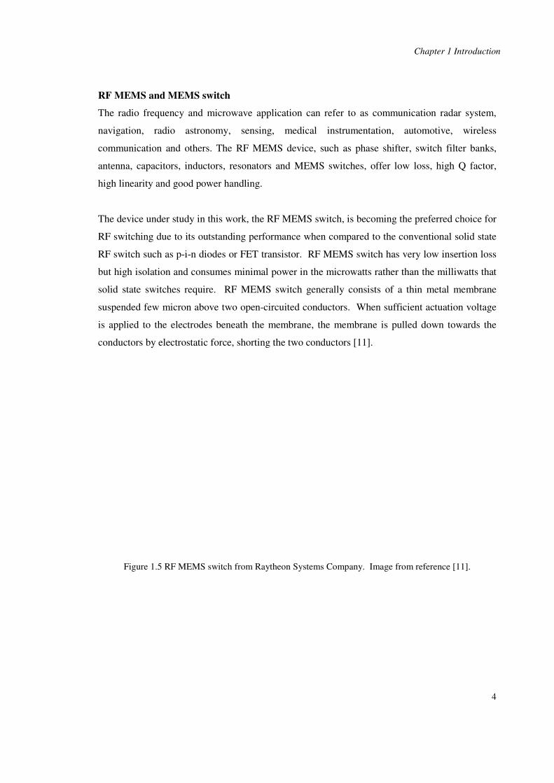
RF MEMS and MEMS switch
The radio frequency and microwave application can refer to as communication radar system,
navigation, radio astronomy, sensing, medical instrumentation, automotive, wireless
communication and others. The RF MEMS device, such as phase shifter, switch filter banks,
antenna, capacitors, inductors, resonators and MEMS switches, offer low loss, high Q factor,
high linearity and good power handling.
The device under study in this work, the RF MEMS switch, is becoming the preferred choice for
RF switching due to its outstanding performance when compared to the conventional solid state
RF switch such as p-i-n diodes or FET transistor. RF MEMS switch has very low insertion loss
but high isolation and consumes minimal power in the microwatts rather than the milliwatts that
solid state switches require. RF MEMS switch generally consists of a thin metal membrane
suspended few micron above two open-circuited conductors. When sufficient actuation voltage
is applied to the electrodes beneath the membrane, the membrane is pulled down towards the
conductors by electrostatic force, shorting the two conductors [11].
Figure 1.5 RF MEMS switch from Raytheon Systems Company. Image from reference [11].

Chapter 1 Introduction
5
1.3 Motivation of this work
The testability and reliability of the MEMS devices are crucial for quality control and long term
application of the devices. This work addresses the issue of testability and reliability of a
tunable RF MEMS filter using RF MEMS switch, which unlike electronics integrated circuit,
MEMS switch is based on interaction between electrical and mechanical components of the
device.
Blanton et al. first addressed the issue of MEMS reliability and testing in 1997 where attempts
were made to map MEMS structural defects and the resulting behaviours with contaminations
during the fabrication process [12]. Blanton et al. suggested that the MEMS defects could be
categorized according to the faulty behaviour classes. Then, with the available fault classes, the
test methodologies could be developed to ensure the reliability of the MEMS devices.
With more understanding of the possible MEMS defects and their effect on the system response,
work on a Built-In-Self-Test (BIST) MEMS have started recently. Blanton et al. has developed
an algorithm to detect faulty MEMS microaccelerometer on a modularized design, where the
sensing elements of the microaccelerometer are divided into standalone segments [13]. By
applying certain test pattern (a combination of ON and OFF modules), the modules that are
faulty could be detected. In [14], Xiong et al. proposed a Built-In-Self-Repair (BISR) technique
that enables the microaccelerometer to switch to redundant module when defect occurs.
Most previous work on MEMS reliability focused on micro-accelerometer and resonators which
exhibit the basic elements of MEMS, but proper mapping between possible physical defects with
the RF MEMS filter response has been lacking. The defects of the RF MEMS filter could occur
on the filter structure or the MEMS switch used for tuning the filter. By analyzing the faulty RF
filter output responses, some of these defects can be identified. Hence, with a library of
common defects and the resulting defective output, if a defective response is detected right after
device fabrication it can be quickly mapped to the defect that causes it. The defects is identified
and corrected during normal operation of the device. Admittedly, this technique is only possible
for common defects and does not cater for multiple defects but even with this limitation the
reliability of RF MEMS filter can be potentially improved.
Chapter 1 Introduction
6
1.4 Objective of this work
This work addresses the reliability of the tunable RF MEMS filter, where the possible common
defects during fabrication and normal operation of the device are analyzed and classified
according to the nature of the defects.
The effects of all these defects on the filter response are then analyzed via simulation so that:
1. The impact of each defect can be assessed and thus allowing the designer to optimize the
design in certain area which is more susceptible to the defects.
2. In future, the defects can be identified by just analyzing the faulty response, or at least
the general location and type of the defect that causes the filter faulty behaviour.
3. A build-in-self-testable and repairable technique can be developed for MEMS switch
failure.
After analyzing the possible defects and effects on the RF filter, a Built-In-Self-Repair technique
is developed so that the device can ‘repair’ itself in the event of MEMS switch failure.
Although the study carried out in this work is specifically for a tunable three poles Chebyshev
bandpass filter, the methodology used in this study can be replicated for other filter devices.
This study also demonstrates how the reliability of a RF device can be analyzed and how failure
analysis can be used for the development of built-in-self-repair mechanism with some device
design changes.

Chapter 1 Introduction
7
1.5 Thesis Overview
This chapter starts with an introduction to the thesis. It gives a summary of the MEMS
technology, the advantages and challenges of MEMS and the motivation for this work.
In Chapter 2, the first part reviews the design and development of the tunable RF MEMS filter.
The second part discusses the testing methods of the RF MEMS filter.
The simulation set-up and various tests that were carried out are summarized in Chapter 3. This
chapter will include the description of the tunable filter under test, the setting of the test, the
software that is being used, the testability of the fault and failure mode in this setting, the
combination fault mode that will be tested, and the limitation of this methodology.
Chapter 4 summarizes the results and observations from the simulation, and discusses different
faults as well as the effects they have on the filter response. These faults include the fault caused
by particulate contamination, geometric variation broken structure, switch stuck-at-on, switch
stuck-at-off and a combination of the fault mode.
Chapter 5 presents a Build-In-Self-Repairable filter design which is able to maintain the filter
functionality even when the MEMS switch used to tune the filter fails. This is made possible
using the “redundant structures” approach. The limitation of this design is also listed.
Chapter 6 concludes the work and discusses further work in this research area.

Chapter 2 Literature Review
8
Chapter 2
2. Literature Review
This chapter reviews the current development of the tunable RF MEMS filter. Then the current
test method based on induction fault analysis for MEMS devices is presented and related to the
RF MEMS filter.
2.1 Current development of Tunable MEMS Filter
Parameters such as signal-to-noise ratio, selectivity of signal, linearity and insertion loss are
optimized when designing a tunable radio frequency filter for the transceiver of multi-channel
communication systems. To tune the filter, varactor (tunable capacitor) and MEMS switches,
and in some cases p-i-n diodes, can be used.
When different biasing voltage is applied to a varactor, the capacitance of the varactor will
change. Examples of varactor used for tuning filter include those by Borwick et al. [15] which
has a good quality factor value of more than 100 and by Kraus et al. [16] which includes
varactor together with filter fabrication giving a good 35% tuning range with constant factional
bandwidth. For Barium Strontium Titanate (BST) thin film type varactor, changing the biasing
voltage of the varactor will alter the value of the dielectric material thereby changing the
capacitance. Figure 2.1 shows a BST varactor designed by Nath et al. [17]. The varactor
requires biasing voltage between 0 V to 200 V to give good return loss of better than 13 dB over
the tuning range. Commercial varactor SMV1763 manufactured by Skyworks Solutions Inc.
was used in the tunable filter developed by Zhang and Xue [18], as shown in Figure 2.2. The

Chapter 2 Literature Review
9
varactor capacitance can be tuned from 1.8 to 9 pF over a 5 V bias range. The filter gives an
insertion loss of less than 3.4 dB and the return loss of better than 10 dB over the tuning range.
Figure 2.1 Photograph of the tunable combline bandpass filter from [17].
Figure 2.2 Proposed tunable dual-band filter using non-uniform microstrip line from [18].
MEMS switches can be used to change RF filter capacitive and inductive behaviour by breaking
or extending filter structures. For example, Nordquist et al. [19] fabricated a tunable X-band
combline filter where the inner three resonators can be extended using MEMS switches to make
the combline longer, as shown in Figure 2.3. This has the effect of increasing the coupling
effects of the resonators and thus the frequency response of the filter. In [20], a switched filter
bank is designed so that it can be switches to three different fixed center frequencies using a
single-pole triple-throw (SP3T) MEMS switch as shown in Figure 2.4. In the tunable filter
designed by Entesari et al. [21] shown in Figure 2.5, commercially available MEMS switches
from Radant MEMS Inc. were used to switch between capacitor banks.

Chapter 2 Literature Review
10
Figure 2.3 (Left) optical micrograph of completed RF MEMS filter from [19]. Insert: RF MEMS
switches. (Right) (a) Insertion loss and (b) return loss.
(a) (b)
Figure 2.4 (a) Photograph of the SP3T, (b) The overall layout of the filter from [20].
Figure 2.5 (Left) Layout of the two-pole tunable filter on a 62-mil FR4 substrate (100 mm x 60 mm).
(Right) Photograph of the MEMS switch from Radant MEMS inc. mounted to the FR4 substrate [21].

Chapter 2 Literature Review
11
Previous work in the field has generally indicated MEMS switch as the better performing RF
tuning method as compared to varactors, p-i-n diodes and FET transistor. While MEMS switch
has the advantage of low insertion loss and high isolation, current work on the MEMS switch
focuses on improving the switch biasing lines design in further minimize insertion loss,
improving the switch linearity and enhancing the lifetime of the switch. There is also an
emerging trend where tunable filter is designed with high quality, commercially available
external MEMS switches.

Chapter 2 Literature Review
12
2.2 Current Development of Testing Method of MEMS
There is an emerging interest in the issue of MEMS testing methodologies, which is uncommon
as unlike electronics integrated circuit, there are diverse MEMS devices based on interaction
between different physical domain including electrical, mechanical, optical, thermal, chemical
and fluidic. Work carried out in the field so far suggested that the development of cost effective
reliability testing techniques for MEMS is an important factor to ensure successful mass-
production of the devices.
The development of MEMS testing methodology follows the footprint of its silicon based
integrated circuit counterparts [22-26]. These methods generally analyze the defective
behaviours of the device and inspect the device under the scanning electron microscope for
particulate contamination, broken structures and geometrical error which may lead to the cause
of defects.
In an effort to address comb-driven MEMS micro-resonator reliability, Blanton et al. [12, 13,
27-30] extends the testing method introduced by Ohletz for integrated circuit testing [26]. The
method, called the “Contamination and Reliability Analysis of Microelectromechanical Layout”
or CARAMEL, involves familiarization with the manufacturing process, contamination
properties and microstructure layout of the microresonator. With these three inputs, the
fabrication process is simulated using a proposed “Contamination-Defect-Fault” or CODEF
simulator to predict the resulting shuttle, comb finger and flexure defects. The defective
microstructure is then simulated using ABAQUS to investigate their effects on the device
response. Figure 2.6 shows the flowchart of the defect analysis process. This work included
that some defects cause catastrophic changes in resonator behaviour, others cause subtle or
insignificant changes in behaviour but might have some implications on long term reliability,
and the impact of some defects cannot be predicted with mechanical simulation alone but require
experiment with real defective MEMS. The CARAMEL method is then improved with the
addition of electrical simulation using HSPICE in [27-30]. Electrical simulation is incorporated
to determine the electrical misbehaviour of the comb-drive micro-resonator that cannot be
detected using mechanical simulation only. With the fault model data in hand, when a device
fails the source of the defects can be quickly determined and if possible removed by comparing
the actual test data with the model data.

Chapter 2 Literature Review
13
Figure 2.6 Contamination analysis of Microelectromechanical systems (CARAMEL).
Deb and Blanton [31, 32] have also analyzed the failure source in surface-micromachined
MEMS device such as micro-resonator and micro-accelerometer. Failures on these devices that
are being investigated include sensor finger stiction, particulate contamination, and etch
variations. These failures are further classified as anchor defect on flexure beam, shuttle,
movable finger, broken beam defect or inter-finger defect.
Courtois et al. [33, 34] investigated the testing methodology for MEMS electro-thermal
converter and resonant beam force sensor using the behaviour model and HDL-A language to
model the devices and their possible defects. The HDL-A together with input stimulus is input
into the mixed-mode multi-level simulator to obtain faulty device graphical interface. The
extended fault-based testing to both bulk and surface micromachined systems are done by Mir,
Charlot and Courtois [34, 35]. There are two main groups of faults are being considered: faults
affecting the MEMS gauge and faults affecting the microstructure that supports the gauge.
Rosing et al. [36-39] proposed a validation methodology which is extended the mixed signal and
analogue integrated circuit fault simulation techniques. The method includes behavioural
modeling techniques with compatible electrical simulators and data classification for failure
mode and effect analysis on MEMS pressure sensor and comb-drive resonator. The layout of the
device is described using the lumped level modeling. Then component level modeling is used to

Chapter 2 Literature Review
14
obtain the complete behaviour model of the device which is then used for modeling the fault of
the devices. Once the fault model of the device is obtained, they are used for developing design-
for-testability or built-in-self-test techniques for the device.
Figure 2.7 Flowchart of the proposed test method from Rosing [36].
Apart from test methodology development, work on built-in self-repairable (BISR) techniques
for MEMS has begun. Xingguo Xiong et al. in [14, 40] proposed a new microaccelerometer
layout that has a built-in self-test (BIST) function which compares a faulty behaviour with
simulated data pre-stored on the device. Once defect is detected, the device has a BISR
mechanism which enables the microaccelerometer to switch to the redundant module.
In summary, the stages in developing testing method for MEMS devices are as follows.
1. Common of defects in MEMS device are identified.
2. Effects of the defects on the behaviour of MEMS elements are analyzed and classified.
3. Simplified fault model of MEMS elements is developed. Realistic wafer-level tests are
done on MEMS components to investigate the incipient failure condition.
4. A test methodology is developed to determine if the device is operating correctly.
5. Some built-in tests for in-service verification of component functional correctness are
developed to improve the testability of device.
6. Eventually, with a good built-in-self-testing mode, a built-in self-repairing technique can
be developed.
Development of testing method and fault modeling for MEMS devices are made complicated by
the multi-domain (electromagnetics, mechanical, thermal and others) nature of MEMS, the
infinite possibilities of defects and the need to be familiar with the device fabrication process.
However, once the common defects and their corresponding impact on the device response are
known when a device fails the source of the defects can be quickly determined. In the following
chapters, testing challenges, methodologies and self-repairing strategy for RF MEMS filter will
be investigated.
Physical layout
of device
device
Lumped
modeling
Component
level modeling
Behaviour
modeling
modeling
Fault
modeling
Parameter
analysis

Chapter 3 Methodology
15
Chapter 3
3. Methodology
The work in this thesis focuses on developing fault models for the RF MEMS filter which can be
used for identification defects from the filter defective response. From these work, a built-in-
self-repairing strategy for the filter is then proposed.
This chapter describes the RF MEMS filter structure under investigation and how software
simulation is used to study the common defects and their effects on the filter behaviour.
3.1 RF MEMS Filter under study
Radio Frequency Micro-Electro-Mechanical system or RF MEMS filter is a device that
eliminates undesired frequencies from the received signal thus only allowing the desired
frequencies to pass through it. RF MEMS filter is fabricated using micro-fabrication technology
integrated with MEMS micro-switches which are used for tuning its frequencies.
The RF MEMS filter under investigation is a 3-pole Chebyshev bandpass filter [41] fabricated
on a 0.52 mm thick quartz substrate with dielectric constant of 3.78. The microstrip on the filter
is made of 0.003 mm thick gold with the conductivity of 40900000 S/m. The design of this filter
is based on the half-wavelength hairpin resonator topology with three hairpin resonators
connected to two feedlines for the input and output of the signal. The tips of each hairpin
resonator can be extended with three narrow line segments with the length of 0.50 mm apart,
which can be connected to each other using the RF MEMS switches. Figure 3.1 shows the
layout of the RF MEMS filter under investigation.

Chapter 3 Methodology
16
Figure 3.1 Layout of the filter under study with the important part being labeled and the labeling of the
number of MEMS switches.
The hairpin resonators are half wavelength of the required center frequency. The following is
the formula for calculating the wavelength of the length value for center frequency of the hairpin
resonator.
(1)
where λ is the wavelength of the resonator, c is the speed of light in meter per second, fc is the
center frequency of the resonator of the filter, ε is the effective dielectric constant. The half-
wavelength of the resonator’s arm is calculated as 1/2 of the hairpin resonator wavelength.
The turns of the hairpin resonator are wider than the hairpin arms in order to reduce the
resistance for the electrons that flow through the microstrip. As shown in Figure 3.2, the 0.05
mm wide narrow line segments at the tips of the hairpin resonator can be connected or
disconnected using MEMS switch to alter the electrical length of the half-wavelength hairpin
ελ
cf
c=

Chapter 3 Methodology
17
resonator. These segments are 0.05 mm apart, in accordance to the RF MEMS switch actuation
size so that the switch pad is large enough to connect one narrow line segment to the adjacent
narrow line segment. Connecting the narrow line segment at the tip of the hairpin resonator with
second line segment will decrease the center frequency of the filter. With all the three narrow
line segments connected together, the center frequency of the filter will decrease further.
A 50 ohms signal input feedline/tapline is connected to the first hairpin resonator through a thin
line segment that act as an inductor to provide the required external quality factor for the filter.
Similarly, a signal output tapline is connected to the last hairpin resonator through another thin
line segment. The location of the tapline connected to the hairpin resonator is determined from
the value of the external quality factor of the design specification of the filter.
Figure 3.2 The narrow line segments, biasing line, grounding pads, grounding line of the RF MEMS
switches that are located at the tip of the resonator.
The following section is a step-by-step demonstration on how this filter is designed, starting
from the design theory of a microwave filter.

Chapter 3 Methodology
18
)(1
1)(
2221
Ω+=Ω
nFjS
ε
3.2 Design Concepts for a microwave filter The design theory of a microwave filter will be discussed, starting from its filter transfer
function and its lowpass prototype. For a given filter specification, the design parameters will be
explained. The final filter is a 3-pole Chebyshev bandpass filter as from reference [41], consists
of hairpin resonators in microstrip structure. The filter is made tunable using
Microelectromechanical systems (MEMS) switches. The design consideration for a tunable
filter is given.
3.2.1 Filter Transfer Function
Two-port filter network characteristics can be written as an amplitude transfer function given as
(2)
where ε is the ripple constant. Fn(Ω) is the filtering characteristic function that will be described
in the following section. Ω is the frequency variable and is equal to 1 radian per second at the
cutoff frequency.
The rational function for the linear time-invariant network is defined as follows:
(3)
where D(p) is a Hurwitz polynomial where the roots (or zeros) are located in the left half-plane
of the complex plane. The roots of zero of N(p) may occur anywhere on the entire complex
plane. The value of p which causes the function to become zero is the zero of the function.
When the function S21(p) to become infinite, the values of p in the denominator D(p) function are
singularities (poles) of the function. When the function of S21(p) becomes zero, the values of p
in the numerator N(p) function are the roots of the function.
)(
)()(21
pD
pNpS =
Chapter 3 Methodology
19
= −
εη
1sinh
1sinh 1
n
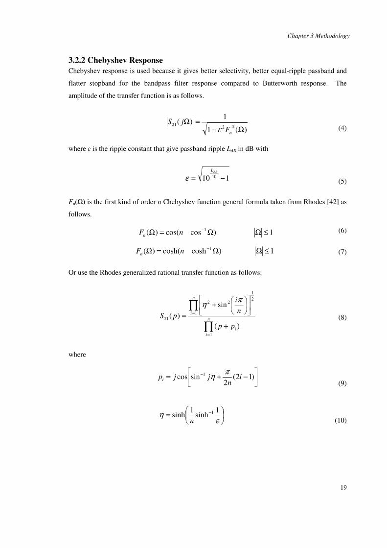
3.2.2 Chebyshev Response
Chebyshev response is used because it gives better selectivity, better equal-ripple passband and
flatter stopband for the bandpass filter response compared to Butterworth response. The
amplitude of the transfer function is as follows.
(4)
where ε is the ripple constant that give passband ripple LAR in dB with
(5)
Fn(Ω) is the first kind of order n Chebyshev function general formula taken from Rhodes [42] as
follows.
(6)
(7)
Or use the Rhodes generalized rational transfer function as follows:
(8)
where
(9)
(10)
)(1
1)(
2221
Ω−=Ω
nFjS
ε
110 10 −=ARL
ε
1)coscos()(1 ≤ΩΩ=Ω −
nFn
1)coshcosh()(1 ≤ΩΩ=Ω −
nFn
∏
∏
=
=
+
+
=n
i
i
n
i
pp
n
i
pS
1
1
2
1
22
21
)(
sin
)(
πη
−+= − )12(
2sincos 1
in
jjpi
πη

Chapter 3 Methodology
20
3.2.3 Chebyshev Lowpass Prototype Filter
Chebyshev lowpass filter serves as a prototype for designing Chebyshev bandpass filter with
frequency and element transformation. Hence, the element values in the Chebyshev lowpass
prototype filter have to be calculated first before the design of the Chebyshev bandpass filter.
The following Figure 3.3 showing the two forms of an n-pole lowpass prototypes for n-pole
filter response.
or
(n even) (n odd)
(a)
or
(n even) (n odd)
(b)
Figure 3.3 (a) Lowpass prototype filters for all-poles filter with a ladder network structure and (b) its dual.
The Chebyshev lowpass prototype filter transfer function is computed with the passband ripple
LAR and the cutoff frequency of 1. The lowpass prototype element values denoted as ‘g’ values
can be computed using the following formula.
(11)
(12)
for i = 2, 3, … n
(13)
0.10 =g
=
ng
2sin
21
π
γ
−+
−
−
=− )1(sin
)32(2
sin)12(2
sin41
221 in
in
in
gg
i
i πγ
ππ

Chapter 3 Methodology
21
(14)
where
(15)
(16)
where n is the number of the pole for the filter. The value of n can be determined by
(17)
where LAS is the minimum stopband attenuation. Using the formula listed below to calculate the
passband ripple, the minimum passband return loss is LR.
(18)
3.2.4 Tunable bandpass filter design
The bandpass filter consists of half-wavelength resonators folded into “U” shape. Due to its
folded U-shape structure, it is commonly known as the “hairpin” resonator. This filter design is
a tunable filter design. It is tuned using MEMS switches to reach the required center
frequencies. The design of this filter includes a quartz material with dielectric constant of 3.78
and the thickness of the quartz is 0.52 mm. The targeted center frequencies are 10.0 GHz, 9.6
GHz and 9.3 GHz.
The device-under-test in this study is a 3-pole Chebyshev hairpin resonators filter design with a
fractional bandwidth of 2.0% (FBW=0.02) and a passband ripple of 0.01 dB. The values
obtained from a normalized lowpass filter with cutoff frequency of 1 radian per second are g0=1,
g1=0.6292, g2=0.9703, g3=0.6292 and g4=1.
=+ even for 4
coth
odd for 0.1
21 n
n
gnβ
=
37.17coshln ARL
β
=
n2sinh
βγ
110
110cosh
cosh
11.0
1.01
1 −
−
Ω≥ −
− AR
AS
L
L
n
( )dBL RL
AR
1.0101log10 −−=

Chapter 3 Methodology
22
With these normalized values, the bandpass design parameters are then calculated using the
following formulae:
(19)
(20)
(21)
where Qei is the input signal external quality factor, Qeo is the output signal external quality
factor, and Mi,i+1 is the coupling coefficient value between the resonators, n is the number of
poles in the filter design, and FBW is the fractional bandwidth of the passband. Fractional
bandwidth (FBW) is calculated using the following equation:
(22)
where f2(-3dB) is the upper limit of the -3 dB of the passband and f1(-3dB) is the lower limit of the
-3 dB of the passband.
For the given fractional bandwidth and normalized values, the calculated input quality factor
(Qei) and output external quality factor (Qeo) are both 31.46. The coupling coefficient between
the first resonator and the second resonator (M1,2) is 0.02560. The coupling coefficient value
between the second resonator and the third resonator (M2,3) is also 0.02560.
The guided wavelength of the microstrip filter is calculated using the formula (1). The half-
length of the resonator is about a quarter length of the guided wavelength λ. The width of the
hairpin resonator is 0.5 mm, but the folding area has a width of 0.8 mm. The size of the hairpin
resonator without the narrow line segment is 4.8 mm in length and 1.5 mm in width.
The three narrow line segments located on the tip of the resonator is for the tuning of the three
different center frequencies. The width of the narrow line segments is 0.05 mm. The length of
first narrow line segment is 0.50 mm. The length of second and the third narrow line segments
FBW
ggQei
10=
FBW
ggQ nn
eo1+=
1- to1for 1
1, nigg
FBWM
ii
ii ==+
+
)3(1)3(2
)3(1)3(2
dBdB
dBdB
ff
ffFBW
−−
−− −=

Chapter 3 Methodology
23
is 0.20 mm. The gap between the two narrow line segments has a size of 0.05 mm. This is
needed for the implementation of the MEMS switches for tuning the length of the wavelength in
the resonators together with the biasing line for the MEMS switches. The biasing line for the
MEMS switches is designed together with the narrow line segments.
As for the biasing circuit for the MEMS switch, the biasing circuit is designed as far as possible
from the narrow line segment. The biasing line should not be longer than ¼ of the wavelength
of the filter; this is to prevent spurious resonant peaks occurring close to the desired filter’s
center frequency.
External quality factor Qe
The external quality factor for both the input and output are obtained using the tapline connected
to the first resonator and a weak coupling at the output end, as shown in Figure 3.4. The Qe is
calculated by varying the tap position t as shown in the following figure.
(a) (b)
Figure 3.4 (a) Layout of the resonator to compute external quality factor value. t is the tap position of the
tapline. This layout will give the frequency response as in (b).
The external quality factor is computed based on the simulated center frequency and the 3 dB
bandwidth using the formula
)3(1)3(2 dBdB
ce
ff
fQ
−− −= (23)
Chapter 3 Methodology
24
22
22
lowhigh
lowhigh
ff
ffM
+
−=
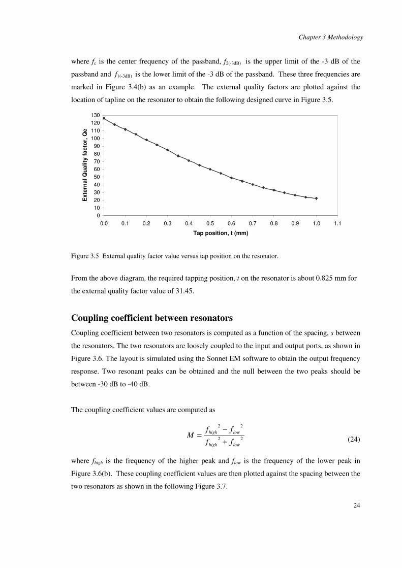
where fc is the center frequency of the passband, f2(-3dB) is the upper limit of the -3 dB of the
passband and f1(-3dB) is the lower limit of the -3 dB of the passband. These three frequencies are
marked in Figure 3.4(b) as an example. The external quality factors are plotted against the
location of tapline on the resonator to obtain the following designed curve in Figure 3.5.
0
10
20
30
40
50
60
70
80
90
100
110
120
130
0.0 0.1 0.2 0.3 0.4 0.5 0.6 0.7 0.8 0.9 1.0 1.1
Tap position, t (mm)
Ex
tern
al
Qu
ali
ty f
ac
tor,
Qe
Figure 3.5 External quality factor value versus tap position on the resonator.
From the above diagram, the required tapping position, t on the resonator is about 0.825 mm for
the external quality factor value of 31.45.
Coupling coefficient between resonators
Coupling coefficient between two resonators is computed as a function of the spacing, s between
the resonators. The two resonators are loosely coupled to the input and output ports, as shown in
Figure 3.6. The layout is simulated using the Sonnet EM software to obtain the output frequency
response. Two resonant peaks can be obtained and the null between the two peaks should be
between -30 dB to -40 dB.
The coupling coefficient values are computed as
(24)
where fhigh is the frequency of the higher peak and flow is the frequency of the lower peak in
Figure 3.6(b). These coupling coefficient values are then plotted against the spacing between the
two resonators as shown in the following Figure 3.7.

Chapter 3 Methodology
25
(a) (b)
Figure 3.6 (a) Layout for measuring the coupling coefficient value between two resonators. S is the
spacing between the two resonators. (b) Output frequency response that is given by the layout of the
resonators.
0
0.01
0.02
0.03
0.04
0.05
0.06
0.07
0.08
0.09
0.1
0.11
0.1 0.2 0.3 0.4 0.5 0.6 0.7 0.8 0.9 1 1.1
Spacing between the resonators, S (mm)
Co
up
lin
g c
oeff
icie
nt
valu
e, M
Figure 3.7 Spacing between the resonators versus the coupling coefficient value between the first
resonator and the second resonator.
The least-squares second- or third-order polynomial function can be fitted to the data shown in
Figure 3.7. The fitted curve should pass through the data points with very low residual error.
Hence, the n-th order polynomial function with a R-squared value of closest to 1 is chosen as the
best-fit curve.

Chapter 3 Methodology
26
The required value of the coupling coefficient is 0.02560. The design specification of the filter
requires 0.825 mm spacing between the resonators. This is the same for both the coupling
coefficient values of M1,2 and M2,3.
Simulation results
After obtaining the required spacing between the resonators and the location for the tapline on
the resonator, three of the resonators are arranged into the required layout together with the input
and output taplines. With the shortened on the narrow line segments on the second resonator,
the three poles hairpin resonator Chebyshev bandpass filter (Figure 3.1) with fractional
bandwidth of 2% and ripple of 0.01 is obtained with the tuning center frequencies of 10.0 GHz,
9.7 GHz and 9.3 GHz as in the following Figure 3.8.
-50
-45
-40
-35
-30
-25
-20
-15
-10
-5
0
8.5 9 9.5 10 10.5 11
Frequency (GHz)
Ma
gn
itu
de
S11 when all switches are OFF S21 when all switches are OFF
S11 when ODD number switches are ON S21 when ODD number switches are ON
S11 when all switches are ON S21 when all switches are ON
Figure 3.8 Simulated results for output frequency response of the filter with all the tuning.

Chapter 3 Methodology
27
3.3 MEMS Switch for RF Filter
MEMS switches are used to connect or disconnect the narrow line segment to tune the center
frequency of the filter. The MEMS switch used for the filter under study was developed in [43]
and is as shown in Figures 3.9 (schematic) and 3.10 (actual photograph). It is a direct contact
type switch as opposed to capacitive type. The size of the switch is about 0.5 mm x 0.32 mm
with the signal line width of 0.05 mm and thickness of 3 µm. The switch is built on the same
substrate as the filter. Its contact bar is made of gold with resistance of about 2 ohms and is
connected to the actuation pad through a thin dielectric membrane. The contact bar is held 1.2
µm above the two narrow line segments (labeled S in the Figure 3.9) of the filter. When a
biasing voltage of 35 V is applied between the actuation pad and ground plate (labeled G), the
pad together with the gold contact bar will be pulled down by electrostatic force, thus connecting
the filter’s two narrow line segments. The switch shows isolation of 8 dB and insertion loss of
0.5 dB at 20 GHz. At cold switching, the lifetime of the switch is approximately 107 cycles [44].
After that, wear and erosion occurs at the contact surface and causes the switch to fail. The
lifetime of the switch during hot switching is 105 cycles with the conduction of the current of
50mA [44].
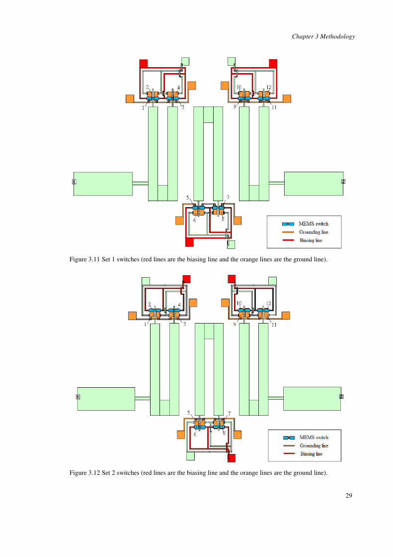
The switches on the filter are divided into two sets. Set 1 consists of the switch with odd
numbering and Set 2 consists of switch with even numbering as shown in Figure 3.11. When
Set 1 switch is turn ON, the center frequency of the filter will be tuned to 9.6 GHz. When both
Set 1 and Set 2 are turned ON, the center frequency will be further lowered to 9.3 GHz. The
biasing lines of the RF MEMS also affect the filter behaviour because it is fabricated using the
same material as the filter. The biasing lines were designed before adjusting the external quality
factor values and the coupling coefficient values of the filters. Figure 3.11 shows the biasing
lines together with the ground plate for Set 1 switches and Figure 3.12 shows the biasing lines
together with the ground plate for Set 2 switches.

Chapter 3 Methodology
28
Figure 3.9 Schematic view of the RF MEMS switch from Reference [43].
Figure 3.10 Photograph of the RF MEMS switch under inspection microscope [43].
Chapter 3 Methodology
29
Figure 3.11 Set 1 switches (red lines are the biasing line and the orange lines are the ground line).
Figure 3.12 Set 2 switches (red lines are the biasing line and the orange lines are the ground line).

Chapter 3 Methodology
30
3.4 Fault simulation and Modeling
The effect of different possible fault during fabrication and normal operation on the RF MEMS
filter behaviour were investigated via simulation using Sonnet Suite Version 11.52 software
[45]. From the simulation results, the faulty behaviours are classified according to their causes
and their effects. This method of fault study is adopted from the inductive fault analysis
approach proposed by Blanton et al. in [13] to study the defect and their effects on the comb-
drive MEMS accelerometer. In their work, firstly the layout, the contaminations and fabrication
process of the MEMS are input into a simulator to simulate the effects of contamination and
fabrication process on the device structure. Then a finite element analysis is carried out to
simulate the mechanical performance of the defective structure. Next, electrical simulation for
the defective device is simulated using HSPICE. Finally, the misbehaviour classifications are
done according to the structural defects, process step classification, probabilities of occurrence
and mechanical and electrical misbehaviour of the device. With these data available, it was
shown that future defects detection and rectification can be carried out quickly.
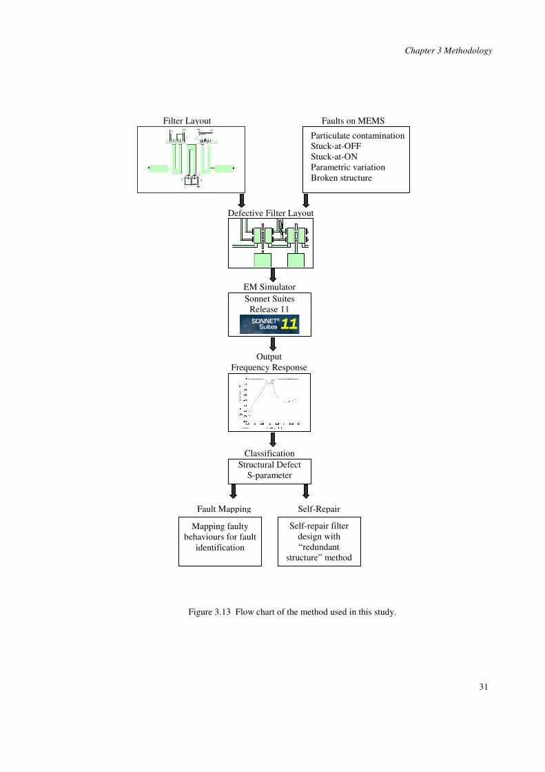
Similarly for studying the defects and faulty behaviour of RF MEMS filter in this work, first the
possible structural defects such as broken structures and geometrical error due to defective
fabrication process are introduced to the filter layout. Then, electromagnetic finite element
analysis is performed on the faulty filter structure using Sonnet software for the S-parameter of
the filter. Loss of tenability and performance degradation of the filter due to MEMS switch
malfunction is also studied in similar manner. Mechanical and electrical analyses on the RF
filter were omitted as RF MEMS filter operation is solely electromagnetic in nature. The faulty
behaviours of the defective filter are then classified according to the cause of defects and effects
on filter performance. This is a novel attempt on applying the inductive fault analysis on RF
MEMS filter. Figure 3.13 shows the methodology undertaken by this work.
Through this study of the defects and the resulting faulty behaviour of the filter, it may enable:
1. Quick prediction of the type and location of defects in future by analyzing the behaviour
of faulty filter. Rectification process can then take place.
2. Filter design to be improved to be less susceptible to common defects.
3. Development of self-test and self-repairing RF MEMS filter that could identify defects
itself and perform in-chip rectifications. This will be demonstrated at a later part of this
thesis.
Chapter 3 Methodology
31
Figure 3.13 Flow chart of the method used in this study.
Filter Layout Faults on MEMS
Particulate contamination
Stuck-at-OFF
Stuck-at-ON
Parametric variation
Broken structure
Defective Filter Layout
Sonnet Suites
Release 11
EM Simulator
Output
Frequency Response
Structural Defect
S-parameter
Classification
Self-repair filter
design with
“redundant
structure” method
Self-Repair
Mapping faulty
behaviours for fault
identification
Fault Mapping

Chapter 3 Methodology
32
3.5 RF MEMS Filter Defects
Admittedly, there are infinite possibilities of defects and combination of them. In this work,
only the common MEMS defects as analyzed in Blanton et al. [13, 30-32] and MEMS switch
failures which is the main cause of failure during normal operation are studied. These defects
are discussed below.
3.5.1 Particulate Contamination
During fabrication process, unwanted materials may be introduced to the device to be fabricated.
Common contamination includes chemical agents and base materials used and environment
particulate. Contamination may cause the disappearance of parts of the structure leading to
pitting (hole) on the surface and on a more severe note may lead to complete breakage of
structure. Contamination may also add unwanted material that leads to small bridging or
bonding of the structures. In this work, particulate contamination defect is simulated as small
square pieces of gold particle randomly placed throughout the surface of the filter structure. For
breakage, it is treated as structural omission in the filter layout.
3.5.2 Geometrical Variation
Geometrical or parametric variation is the deviation of the length, width and height of the filter
structure from intended fabrication specification. The deviation may be caused during masking,
electroplating and etching processes. Mask variation occurs when there is variation in the
frequency, quality and exposure duration of the light-wave that is applied onto the photo resist
mask [46]. Under-etching of the structure happens when the mask is smaller than the required
dimension, therefore retaining unwanted parts on the structure. This may lead to complete filter
failure if the under-etched area bridges the two separate components on the filter structure. Over-
etching occurs when the masked area that is not supposed to be etched is accidentally etched
away. This can happen when the photo-resist protection mask is too small or the concentration of
the etching solution is too thick.
Geometrical variation at the filter’s narrow line segments affect its behavior mostly due to the
segment relatively smaller dimension compared to the rest of the structure. Over or under-
etching of the narrow lines may decrease or increase the quarter-wavelength of the hairpin
resonator thereby changing the center frequency. In severe cases, over-etching may lead to

Chapter 3 Methodology
33
broken structures especially at these lines such as the RF MEMS switch biasing line and the
connection between the tapline and the hairpin resonator.
3.5.3 MEMS Switch Stuck-at-ON and Stuck-at-OFF
MEMS switch failure is perhaps the most probable defect which will occur during fabrication
and normal operating time [47]. During the wet release stage in the fabrication process, the
MEMS switch may get stuck-at-ON due to the strong capillary force that pulls down the contact
pad onto the signal lines for the filter [47]. During normal operating times, repeated switching
between the ON and OFF state accumulates the charges trapped on the substrate, generating
electrostatic force. Over time, these charges are large enough to generate its own electrostatic
force to hold the switch at ON state permanently even without any biasing voltage. The MEMS
switch may get stuck-at-OFF during fabrication if there is a broken biasing line or incomplete
release of the sacrificial layer between the contact bar narrow lines blocking their contact [47].
Switch stuck-at-ON is modeled as a short circuit between the narrow lines segments and the
stuck-at-OFF is modeled as open circuit. A combination of multiple stuck-at-ON and stuck-at-
OFF switch failures can be modeled in this work. But any combination of more than 3 switch
failure is disregarded as the resulting faulty behaviour is indistinguishable. Moreover, once a
switch fails usually the device is rendered useless.
3.5.4 Other Defects
Inter-metallic diffusion may occur on the RF MEMS switch as it is fabricated with two types of
metal - gold and nickel. When inter-metallic diffusion happens, it increases the resistivity of the
switch contact bar. Fortunately, the change in the resistance is insignificant and therefore the
inter-metallic diffusion is not taken into consideration in this study.
Under-cutting of silicon substrate during etching is not common for the filter under investigation
since the substrate for the filter is made of quartz. Under-cutting may only happen on the
actuation pad and the contact bar of the RF MEMS switch. When under-cutting happens, cracks
are observed on the actuation pad and on the contact pad. This might lead to the stuck-at-OFF
fault on the switch.
Chapter 3 Methodology
34
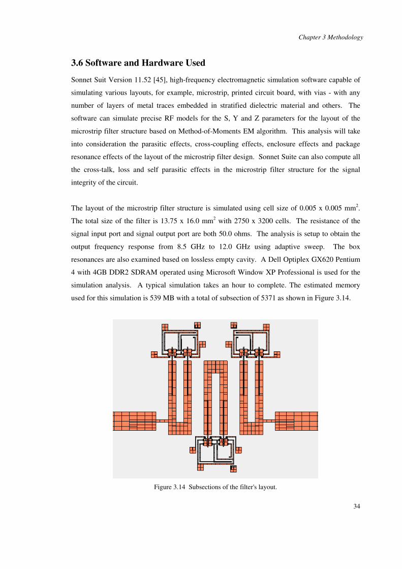
3.6 Software and Hardware Used
Sonnet Suit Version 11.52 [45], high-frequency electromagnetic simulation software capable of
simulating various layouts, for example, microstrip, printed circuit board, with vias - with any
number of layers of metal traces embedded in stratified dielectric material and others. The
software can simulate precise RF models for the S, Y and Z parameters for the layout of the
microstrip filter structure based on Method-of-Moments EM algorithm. This analysis will take
into consideration the parasitic effects, cross-coupling effects, enclosure effects and package
resonance effects of the layout of the microstrip filter design. Sonnet Suite can also compute all
the cross-talk, loss and self parasitic effects in the microstrip filter structure for the signal
integrity of the circuit.
The layout of the microstrip filter structure is simulated using cell size of 0.005 x 0.005 mm2.
The total size of the filter is 13.75 x 16.0 mm2 with 2750 x 3200 cells. The resistance of the
signal input port and signal output port are both 50.0 ohms. The analysis is setup to obtain the
output frequency response from 8.5 GHz to 12.0 GHz using adaptive sweep. The box
resonances are also examined based on lossless empty cavity. A Dell Optiplex GX620 Pentium
4 with 4GB DDR2 SDRAM operated using Microsoft Window XP Professional is used for the
simulation analysis. A typical simulation takes an hour to complete. The estimated memory
used for this simulation is 539 MB with a total of subsection of 5371 as shown in Figure 3.14.
Figure 3.14 Subsections of the filter's layout.

Chapter 4 Simulation Results
35
Chapter 4
4. Simulation Results
In this chapter, the common MEMS defects discussed previously are simulated and their effects
on MEMS filter response are studied. The simulation output of the filter’s S-parameters,
specifically the return (S11) and the insertion loss (S21) parameters for frequency, ranges from
8.5 GHz to 11.5 GHz. The faulty behaviours are classified according to the nature of the defects
and the effects that they bring about to the filter response.
4.1 Particulate contamination
Only particulate contaminations that potentially change the capacitive value of the main MEMS
filter structure are taken into account in this simulation study. Therefore, particles with the size
of less than 5µm in diameter are not considered as they were shown to be rather inconsequential
due to the relatively small size as compared to the filter structure. In this work, 5µm gold
particles are scattered randomly at different parts on the layout of the filter structure to emulate
particulate contamination as gold is the most probable contaminations, since the main structure
of the filter is fabricated using gold.
4.1.1 Particles away from the filter structure
Particles in the region further than 5µm away from the filter structure, as shown on grey in
Figure 4.1 have no significant effect on the response of the filter as well because the particle
cannot generate electromagnetic field that is large enough to affect the electromagnetic field

Chapter 4 Simulation Results
36
pattern of their main filter structure. This has been verified by randomly placing gold particle in
this region, and all simulation results show the filter response is not affected.
Figure 4.1 The region further away from the main structure (grey colour). The particulate contamination
in the grey areas will not show any effect on the output frequency response of the filter.
4.1.2 Particulate on the RF MEMS switch biasing lines
From simulation, it is shown that any particulate contamination on the biasing lines and area
around them, as shown in grey in Figure 4.2 will not affect the response of the filter.
Figure 4.2 RF MEMS switches biasing lines are in the grey regions.

Chapter 4 Simulation Results
37
4.1.3 Particulate on the filter main structure
The main filter structures consist of the taplines, hairpin resonators and narrow line segments at
the end of the resonators. The RF MEMS switch and biasing line are not considered here.
Particulate contamination may lead to surface protrusion and side protrusion. All the MEMS
switches are at the OFF state.
i. Taplines/feedlines
Figure 4.3 shows the layout of the signal input feedline with port 1 and output feedline with port
2. If particle contamination leads to surface protrusion on the edge of the dark grey region on
the feedline, it may reduce the return loss from 25.5 dB to as low as 23 dB. If particle
contamination occurs on the light grey regions, return loss may be increased to 26 dB. However,
if contamination occurs in the white regions, the filter response is not affected. Particle
contamination that causes protrusion on the side of the feedlines leads to a decrease in the return
loss from 25 dB to 22 dB. If particle contamination appears next to the surface mount connector,
it may bounce back the signal from the input/output line, leading to noise and therefore reduce
the value of the return loss further.
(a) (b)
Figure 4.3 Layout of the (a) input signal feedline with port 1 and (b) output signal feedline with port 2.
ii. Hairpin resonators
Any particle on the resonators that causes surface protrusion has insignificant effect on the
frequency response of the filter. However, the particle that caused protrusion on the side of the
resonator will lead to a formation of extra parasitic capacitance, affecting the response of the
filter. Tables 4.1, 4.2 and 4.3 below detail the effect of contamination at the different resonators.
iii. Narrow line segments
Any particle contamination at the narrow line segments does not affect the response of the filter
as long as the contamination does not impede the MEMS switch operation. The details are
presented in Table 4.4. The MEMS switch contact pad is located about 1.2 micrometers above
the narrow line. If the particulate contamination occurs on the line that is covered by the contact
pad, the movement of the contact pad will be impeded, causing the filter to loose its tunability.

Chapter 4 Simulation Results
38
Table 4.1 Effect of particulate contamination at the first hairpin resonator.
On the first hairpin
resonator
S11 S21 Frequency shift Remark
Tip of the resonator, far
from the narrow line
segments
11 dB – 15 dB S21 decreases Lower frequency The increase in the length of the
half-wavelength resonator leads
to the decrease in the center
frequency of the resonator.
The inside of the U-bend of
the resonator
23 dB – 24 dB No significant
change
No significant
shift
Only a minute change in the
bending area.
The outside of the U-bend
of the resonator.
14 dB – 20 dB (from
the edge to the center of
U)
S21 decreases Higher frequency The contamination acts as a
capacitance that shifts the center
frequency to a higher frequency
value.
The connection between the
tapline and the resonator
23 dB – 24 dB No significant
change
No significant
shift
Only a minute change in the
bending area.
Tip of the resonator, close
to the narrow line segments
26 dB – 28 dB (from
narrow line segment to
the side of resonator )
No significant
change
No significant
shift
This actually improves the
external quality factor of the input
signal into the filter.
Side of the resonator tip 25 dB – 28 dB No significant
change
No significant
shift
This actually improves the
external quality factor of the input
signal into the filter.
Note: Please refer to Figure 4.4 for the location of the particulate contamination on first hairpin resonator.

Chapter 4 Simulation Results
39
Table 4.2 Effect of particulate contamination at the second hairpin resonator.
On Second hairpin
resonator
S11 S21 Frequency shift Remark
Tip of the resonator, far
from the narrow line
segments
20 dB – 25 dB (from
the hairpin edge toward
the narrow line
segment)
S21 decreases Lower frequency The increase in the length of the
half-wavelength resonator leads
to the decrease in the center
frequency of the resonator.
The inside of the U-bend of
the resonator
25 dB – 28 dB No significant
change
No significant
shift
Minute change in the bending
area. Does not change the overall
output frequency response.
The outside of the U-bend
of the resonator.
11 dB – 21 dB
(from middle of U-
bend to the edge)
No significant
change
Higher frequency Extra capacitance is introduced
onto the bending area, thus
shifting the center frequency to a
higher frequency.
Tip of the resonator, close
to the narrow line segments
24 dB – 20 dB
(outwards from near the
narrow line segments)
No significant
change
No significant
shift
Similar to the frequency response
of the faultless filter. However,
the coupling coefficient between
the resonators is affected, hence
the decrease in the S11 value.
Tip of the resonator, the
side of the resonator
21 dB to 24 dB
(moving away from the
tip of the resonator)
No significant
change
No significant
shift
Similar to the frequency response
of the faultless filter. This might
have affected the coupling
coefficient between the
resonators, hence the decrease in
the S11 value.

Chapter 4 Simulation Results
40
Table 4.3 Effect of particulate contamination at the third hairpin resonator.
On the third hairpin
resonator
S11 S21 Frequency shift Remark
Tip of the resonator, far
from the narrow line
segments
18 dB - 23 dB S21 decreases Lower frequency The increase in the length of the
half-wavelength resonator leads
to the decrease in the center
frequency of the resonator.
The inside of the U-turn of
the resonator
23 dB – 24 dB No significant
change
No significant
shift
Minute change in the bending
area.
The outside of the U-turn of
the resonator.
18 dB - to 21 dB
(from the edge to the
center of U)
S21 decreases Higher frequency Extra structure acts as a
capacitance that shifts the center
frequency to a higher frequency
value.
The connection between the
tapline and the resonator
23d B – 24 dB No significant
change
No significant
shift
Minute change in the bending
area.
Tip of the resonator, close
to the narrow line segments
26 dB – 28 dB
(from narrow line
segment to the side of
resonator )
No significant
change
No significant
shift
It still has the same center
frequency because this fault does
not affect the coupling coefficient
of between the second resonator
and the third resonator.
Tip of the resonator, the
side of the resonator
25 dB – 28 dB No significant
change
No significant
shift
Improvement is insignificant,
since the narrow line segment is
much longer than the length of
the particle.

Chapter 4 Simulation Results
41
Table 4.4 Effect of particulate contamination at the narrow line segments.
Narrow line segments Surface / Side
protrusion
S11 S21 Frequency
shift
Reason
On narrow line
segments covered by
the contact pad
Surface
(height < 3µm)
No significant
change
No
significant
change
No significant
change
Insignificant if all switches
at OFF state.
However, this
contamination impedes the
switch contacting pad, thus
leading to a stuck-at-OFF
fault when switch needs to
be turned ON.
On narrow line
segments that is not
covered by the contact
pad
Side protrusion
( <10% of the width
of the narrow line)
No significant
change
No
significant
change
No significant
change
No significant effect at any
switching state.
Particulate
contamination located
in the middle of the gap
of two narrow line
segments.
Surface protrusion
( < 10% of the
width of the narrow
line segments, and
height does not
impede the switch)
No significant
change
No
significant
change
No significant
change
No significant effect at any
switching state due to the
small size of the particulate
contamination and the
contamination does not join
the two narrow line
segments together to form a
short circuit.

Chapter 4 Simulation Results
42
Figure 4.4 The location of the particle contamination on the first hairpin resonator.
Tip of the resonator,
close to the narrow line
segments
Sides of the resonator tip
Tip of the resonator, far from
the narrow line segments
Connection between the
tapline and the resonator
Inside of the U-bend of the
resonator
Outside of the U-bend of
the resonator
Outside of the U-bend of
the resonator

Chapter 4 Simulation Results
43
4.1.4 Summary of the effect of particulate contamination
From the simulation analysis, it can be concluded that if the filter is contaminated by randomly
scattering 5µm gold particles at the MEMS switch biasing circuit and at region more than 5µm
away, the filter response would not be affected.
Particulate contamination leads to:
i. surface and side protrusion on the 50 ohm tapline, especially near the surface mount
connector
ii. side protrusion on the tip of the hairpin resonator away from the narrow line segment,
especially those hairpins adjacent to the tapline may lower the return loss.
Some contamination may increase the performance of the filter. This was observed when particle
contamination leads to:
iii. side protrusion near the line segments of the first and third resonators hairpins’ tip
iv. the inner bend of the middle hairpin resonator
Due to symmetry, a side protrusion on the third hairpin resonator will lead to an almost similar
filter response as to when a side protrusion occurs at the first resonator. Similarly, a side
protrusion on the left arm of a resonator will bring about comparable response as to when a side
protrusion occurs on the right arm.
Gold particle contamination of the diameter that is 5µm or less will not have any effect on the
filter response if:
i. it occurs in the region further than 5µm away from the filter structure
ii. it occurs on the biasing lines
iii. it leads to surface protrusion on the filter
iv. it occurs at the narrow line segments (as long as the contamination does not impede
the MEMS switch operation)

Chapter 4 Simulation Results
44
4.2 Physical defects
4.2.1 Broken structures
Parts of the filter structure may be accidentally etched away when the photo-resist mask used is
too small or the concentration of the etching solution is too thick. Over-etching may lead to the
disappearing of parts of the filter, mainly at the narrow line segments due to their smaller
dimension. If breakage occurs at the line segment that is connected to the resonator as shown in
Figure 4.5(a), the filter will have deteriorated insertion and return loss. For example when all the
switches are in the OFF state, the broken narrow line segment leads to return loss of about 7 dB
and shifts the center frequency higher due to the decrease in the length of the resonator. The
deterioration is especially noticeable when the breakage occurs in the second resonator, as
shown in Figure 4.6 (a). Also, since the path from the resonator to the switch-able line segments
is broken, the filter looses its tunability.
If the breakage occurs at the outer line segment as shown in Figure 4.6 (b), the filter is still
tunable though it may suffers minor performance deterioration. Breakage in the middle line
segment is not considered as the MEMS switch contact pad may be large enough to reconnect
the break.
(a) (b)
Figure 4.5 (a) Broken line segment near the tip of the hairpin resonator. (b) Broken microstrip line on the
narrow line segment further away from the hairpin resonator.
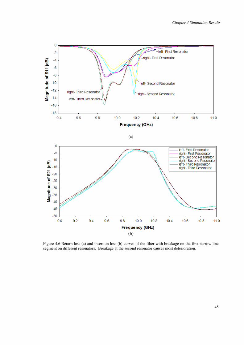
Chapter 4 Simulation Results
45
(a)
(b)
Figure 4.6 Return loss (a) and insertion loss (b) curves of the filter with breakage on the first narrow line
segment on different resonators. Breakage at the second resonator causes most deterioration.

Chapter 4 Simulation Results
46
4.2.2 Short circuit
Though highly unlikely, short circuit caused by under-etching may happen at the gap between
the grounding pad of the MEMS switches’ actuation pad and the narrow line segments as this
location has the smallest gap in the whole structure. When this happens, the current that flows
through the resonator into the narrow line segments will be grounded before it reaches the end of
the tip of the microstrip filter narrow line segment, causing complete filter failure.
Figure 4.7 Under-etching causing short circuits at different part of the narrow line segments. Black dots
represent short circuit caused by under-etching.
4.2.3 Parametric variations
Geometrical errors of between ±15µm on the filter structure caused by etching variation have
been simulated. Analysis of the filter response shows that geometrical errors on the hairpin
resonator, narrow line segments, taplines and biasing lines only shift the center frequency by 1%
at most and cause minor reduction in the return loss.
This is mainly due to the relatively large dimension of the filter structure when compared to the
potential geometrical error. Moreover, since in actual fabrication the geometrical variations will
be much less than ±15µm, this error may be safely ignored.

Chapter 4 Simulation Results
47
4.3 MEMS Switch Failure
MEMS switch failure is perhaps the most probable defect which will occur during fabrication
and normal operating times [47]. During the wet release stage in the fabrication process, the
MEMS switch may get stuck-at-ON due to the strong capillary force that pulls down the contact
pad onto the signal lines of the filter [47]. During normal operating times, repeated switching
between the ON and OFF state accumulates the charges trapped on the substrate, generating
electrostatic force. Over time, these charges are large enough to generates its own electrostatic
force to hold the switch at ON permanently even without any biasing voltage [47]. The MEMS
switch may get stuck-at-OFF during fabrication if there is a broken biasing lines or incomplete
release of the sacrificial layer between the contact bar and narrow lines blocking their contact.
Switch stuck-at-ON is modeled as a short circuit between the narrow lines segments and stuck-
at-OFF is modeled as open circuit. A combinations of multiple stuck-at-ON and stuck-at-OFF
switch failures can be modeled but in this work, any combination of switch failure is disregarded
as the resulting faulty behavior is too complicated to generalize. More importantly, once a switch
fails, usually the device is rendered useless. In addition, though not shown here it was found that
if two or more switches are stuck-at-ON / OFF the response of the filter will be dominated by the
most deteriorated response of the individual defective switches. Therefore, only analysis of one
single switch failure is taken into consideration.
If a MEMS switch which is supposed to be OFF but it got stuck at ON, it causes the length of
the resonator to become longer and hence decreases the center frequency of the filter. For
example, all switches should be turned OFF to tune the filter center frequency to 10GHz but if
switch 1 is stuck-at-ON, the center frequency drops to 9.85GHz. Similarly, any switch which is
stuck-at-OFF will increase the filter center frequency. This effect is especially apparent if the
defective switch is on the middle hairpin resonator. Since the even number MEMS switches (2,
4, 6, 8, 10 and 12) only connect the outer line segments to the hairpin resonators when the odd
number switch (1, 3, 5, 7, 9 and 11) is ON, any defective even number switches will only shows
up when the all the odd switches are connected first.
Table 4.5 shows the simulated parameters of the filter when switch is stuck-at-ON. In this table,
the defective even number switches are considered when the filter is on 9.6 GHz settings (all odd
switches are ON). The defective odd number switches are considered when the filter is on 10.0
GHz settings (all switch are OFF). From the table due to symmetry of the filter design, defects

Chapter 4 Simulation Results
48
in the pairs of switches (1, 11), (2, 12), (3, 9), (4, 10), (5, 7) and (6, 8) produce similar
deterioration in the bandwidth and center frequency and the filter exhibits similar insertion loss.
Defects in the middle hairpin (5, 7) and (6, 8) switch pairs even produce similar return loss
curve.
Table 4.5 Summary of the output frequency response of single stuck-at-ON fault of each switch.
Switch no. Lower -3 dB
(GHz)
Upper -3 dB
(GHz)
Center frequency
(GHz)
S11 (dB) S21 (dB)
1 9.695 10.018 9.8565 3.3 4.796
3 9.771 10.088 9.9295 4.9 3.406
5 9.638 10.036 9.837 3.205 4.86
7 9.633 10.028 9.8305 3.071 5.03
9 9.771 10.088 9.9295 8.559 3.678
11 9.693 10.017 9.855 4.8 5.371
2 9.335 9.651 9.493 3.45 5.0
4 9.395 9.704 9.5495 5.39 3.74
6 9.3 9.664 9.482 4.87 3.64
8 9.299 9.663 9.481 4.81 3.65
10 9.395 9.7035 9.54925 8.18 3.16
12 9.334 9.652 9.493 5.16 6.0

Chapter 4 Simulation Results
49
4.4 Limitation of the analysis
Admittedly, the analysis carried out above was focused on the specific 10 GHz hairpin filter
design. Generalization on the effects of the defects on a common filter will be far too complex
and will require a much more extensive work. This work however, successfully demonstrates
how the analysis on a defective MEMS filter can be conducted. The analysis on defective filter
response carried out in this chapter has:
1. identified the possible effects from the different defects in the filter
2. revealed the depth of impact of each defect, which would allow designer to optimize
design in certain area (e.g. tip of hairpin resonators must be accurate and free from
geometrical error while surface inaccuracy can be tolerated)
3. allowed the defects to be identified, or at least the general location and type of the
defect that causes the filter faulty behavior
4. showed that symmetry of the filter design may hide many defects
5. led to the development of BISR (later chapter) in case of MEMS switch failure
which can be replicated for study into other filter structures.
This analysis does not take into account the combination of two or more faults that may occur
simultaneously. Also, the exact cause and location of the faults cannot be accurately pinpointed
by just looking at the defective response alone. Nevertheless through this work, it offers a good
first guess on the possible causes of the faulty behavior and leads the search for the fault.
In future, a probabilistic design can be used to simulate the effects of the combination of faults
on the behaviors of the device. This is further discussed in Chapter 6 in the future work for this
study.
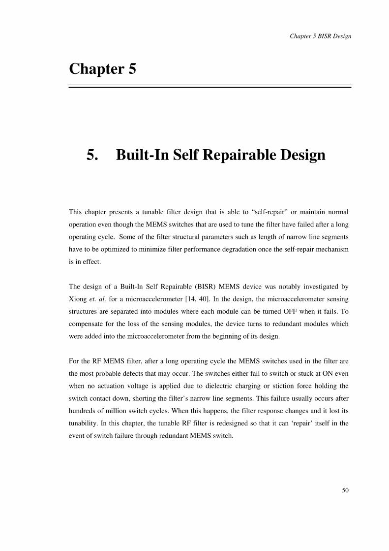
Chapter 5 BISR Design
50
Chapter 5
5. Built-In Self Repairable Design
This chapter presents a tunable filter design that is able to “self-repair” or maintain normal
operation even though the MEMS switches that are used to tune the filter have failed after a long
operating cycle. Some of the filter structural parameters such as length of narrow line segments
have to be optimized to minimize filter performance degradation once the self-repair mechanism
is in effect.
The design of a Built-In Self Repairable (BISR) MEMS device was notably investigated by
Xiong et. al. for a microaccelerometer [14, 40]. In the design, the microaccelerometer sensing
structures are separated into modules where each module can be turned OFF when it fails. To
compensate for the loss of the sensing modules, the device turns to redundant modules which
were added into the microaccelerometer from the beginning of its design.
For the RF MEMS filter, after a long operating cycle the MEMS switches used in the filter are
the most probable defects that may occur. The switches either fail to switch or stuck at ON even
when no actuation voltage is applied due to dielectric charging or stiction force holding the
switch contact down, shorting the filter’s narrow line segments. This failure usually occurs after
hundreds of million switch cycles. When this happens, the filter response changes and it lost its
tunability. In this chapter, the tunable RF filter is redesigned so that it can ‘repair’ itself in the
event of switch failure through redundant MEMS switch.

Chapter 5 BISR Design
51
5.1 Symmetry and Redundancy
The RF MEMS filter designed in this work has symmetries at the switches on the hairpin
resonators’ end. For example in the first resonator, the Switch 3 and 4 are at symmetry with
Switch 1 and 2. Therefore, switching Switch 1 ON produces the same effect as switching Switch
3 ON, and switching Switch 1 and 2 ON is the same as switching Switch 3 and 4. This makes
Switch 3 and 4 the potential ‘redundant’ switches that can be used to ‘repair’ Switch 1 and 2
later. Simulation results in Figure 5.1 below shows that Switch 3 and 4 produces similar filter
response to Switch 1 and 2.
-60
-50
-40
-30
-20
-10
0
8.5 9 9.5 10 10.5 11 11.5 12
Frequency (GHz)
Ma
gn
itu
de
of
S2
1 (
dB
)
3-5-9 ON 1-5-9 ON
Figure 5.1 Insertion loss when Switch 3, 5, and 9 are ON is similar to when Switch 1, 5, and 9 are ON.
-60
-50
-40
-30
-20
-10
0
8.5 9 9.5 10 10.5 11 11.5 12
Frequency (GHz)
Ma
gn
itu
de
of
S2
1 (
dB
)
1-2-5-6-9-10 ON 3-4-5-6-9-10 ON
Figure 5.2 Insertion loss when Switch 1, 2, 5, 6, 9, and 10 are ON is similar to when Switch 3, 4, 5, 6, 9
and 10 are ON.

Chapter 5 BISR Design
52
Similarly, Switch 7 and 8 can replace Switch 5 and 6, and Switch 11 and 12 can replace Switch
9 and 10. Note however, as shown in Figure 5.2, that the filter response is not exactly the same
when the ‘redundant’ switches are used, and some fine-tuning of the filter structure is needed to
ensure similar performance is retained.
5.2 Filter Redesign with BISR
The filter was designed to switch between 9.3GHz, 9.6GHz and 10GHz. However, by using the
symmetry and ‘redundant’ switching as suggested above, the filter switched between 9.6GHz,
9.8GHz and 10GHz. Therefore, the layout of the filter needs to be reconsidered to reposition the
center frequency, and fine-tuning measures added to make the filter perform similarly when
redundant structures are in effect. Before redesigning the filter, the biasing line for each of the
MEMS switches has to be separated so that each of the switches can be independently biased.
The grounding line for the switches remains the same.
5.2.1 Hairpin Resonator
In order to redesign the filter, the resonators are separated and considered individually. Starting
with the first resonator, the length of the second and third narrow line segments are adjusted to
obtain the desired center frequency where:
a. 10 GHz without any switching
b. 9.6GHz when either Switch 1 or 3 is ON
c. 9.3GHz when either Switch 1 & 2 or Switch 3 & 4 are ON
In order to reduce the required length of the second narrow line segment that is connected to
Switch 3, a low impedance area in the middle of the second narrow line segment is introduced.
For the same purpose, a low impedance area is also introduced onto the tip of the third narrow
line segment connected to Switch 4. Figure 5.3 shows the amended layout.
Similarly, the second resonator’s line segments are adjusted to obtain the right center frequency.
However, since the required narrow line segments are not as long as that required by the first
resonator, the low impedance area are not introduced for designing the second resonator. Figure
5.4 shows the layout of the second resonator together with its MEMS switch biasing lines.
Figure 5.5 shows amended the third resonator.

Chapter 5 BISR Design
53
(a) (b)
Figure 5.3 (a) Layout of the filter’s first hairpin resonator together with input signal tapline and weak
coupling on the output signal tapline. (b) The zoomed in on the MEMS switches biasing circuit and the
adjustment of the narrow line segments on the first hairpin resonator.
(a) (b)
Figure 5.4 (a) Layout of the filter's second resonator with weak coupling for both the input and output
signal taplines. (b) Highlight the adjustment of the narrow line segments.
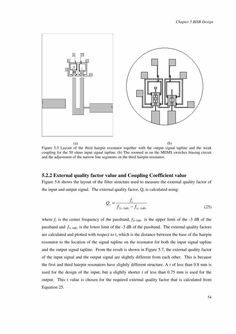
Chapter 5 BISR Design
54
(a) (b)
Figure 5.5 Layout of the third hairpin resonator together with the output signal tapline and the weak
coupling for the 50 ohms input signal tapline. (b) The zoomed in on the MEMS switches biasing circuit
and the adjustment of the narrow line segments on the third hairpin resonator.
5.2.2 External quality factor value and Coupling Coefficient value
Figure 5.6 shows the layout of the filter structure used to measure the external quality factor of
the input and output signal. The external quality factor, Q, is calculated using:
(25)
where fc is the center frequency of the passband, f2(-3dB) is the upper limit of the -3 dB of the
passband and f1(-3dB) is the lower limit of the -3 dB of the passband. The external quality factors
are calculated and plotted with respect to t, which is the distance between the base of the hairpin
resonator to the location of the signal tapline on the resonator for both the input signal tapline
and the output signal tapline. From the result is shown in Figure 5.7, the external quality factor
of the input signal and the output signal are slightly different from each other. This is because
the first and third hairpin resonators have slightly different structure. A t of less than 0.8 mm is
used for the design of the input, but a slightly shorter t of less than 0.75 mm is used for the
output. This t value is chosen for the required external quality factor that is calculated from
Equation 25.
)3(1)3(2 dBdB
ce
ff
fQ
−− −=

Chapter 5 BISR Design
55
(a) (b)
Figure 5.6 Layout of the filter's hairpin resonator together with the signal tapline for weak coupling to
determine the external quality factor value for both (a) the input signal tapline into the modified first
hairpin resonator, (b) the output signal tapline from the modified first hairpin resonator. t is the tap
position of the tapline on the resonator.
(a) (b)
Figure 5.7 External quality factors, Q of the modified resonator versus the length of t for (a) input signal
external quality factor and (b) output signal external quality factor of the filter.
0
10
20
30
40
50
60
70
80
90
100
0.2 0.4 0.6 0.8 1 1.2 1.4
Length of t (mm)
Exte
rnal
Qu
ali
ty F
acto
r, Q
e
0
10
20
30
40
50
60
70
80
90
100
0.2 0.4 0.6 0.8 1 1.2 1.4
Length of t (mm)
Exte
rnal Q
uality
Facto
r, Q
e

Chapter 5 BISR Design
56
To measure the coupling coefficient against the gap between the resonators, the layout shown in
Figure 5.8 is used. All the switches are OFF. The coupling coefficients between the hairpin
resonators, M, are calculated using:
(26)
where fhigh is the frequency of the upper peak and flow is the frequency of the lower peak. These
coupling coefficient values are then plotted against the spacing between the two resonators as
shown in the following Figure 5.7.
(a) (b)
Figure 5.8 Layout of the structure for measuring the coupling coefficient between the two resonators: (a)
between first and second resonators, (b) between the second and third resonators.
As shown in Figure 5.9, the coupling coefficient between the first and second resonators is
different compared to the coupling coefficient between the second and third resonators. This is
because the third resonator designed is slight different from that of the first resonator. Note that
the decrease in the coupling coefficient due to the biasing of the MEMS switches is not taken
into consideration of the design. A gap of less than 0.8 mm between the first and second
resonator is used whilst a gap of less than 0.7 mm between the second and third resonators is
used to achieve a coupling coefficient of more than 0.020. This is to fulfill the design
requirement for the original 3-pole Chebyshev filter.
lowhigh
lowhigh
ff
ffM
22
22
+
−=

Chapter 5 BISR Design
57
0.000
0.005
0.010
0.015
0.020
0.025
0.030
0.035
0.040
0.045
0.050
0.4 0.5 0.6 0.7 0.8 0.9 1 1.1 1.2 1.3
Width of the Gap, W (mm)
Co
up
lin
g C
oeff
icie
nt,
K23
(a) (b)
Figure 5.9 (a) Graph of coupling coefficient value between the first and the second resonators versus the
width of the gap between them. (b) Graph of coupling coefficient value between the second and the third
resonators versus the width of the gap between them.
The redesigned filter is then fine tuned through simulation using Sonnet by:
a. adjusting the location of the signal tapline
b. moving the resonators closer to each other, decreasing the gap and thus enhancing
the external quality factor and the coupling coefficient between the resonators
c. increasing or decreasing the narrow line segment length and low impedance area
until an optimized filter response is obtained. The final filter design is shown in Figure 5.10.
Figure 5.10 Layout of the redesigned filter with BISR.
0.000
0.005
0.010
0.015
0.020
0.025
0.030
0.035
0.040
0.045
0.050
0.4 0.5 0.6 0.7 0.8 0.9 1 1.1 1.2 1.3
Width of the Gap, W (mm)
Co
up
ling
Coeff
icie
nt,
K12
Chapter 5 BISR Design
58
5.3 Performance of the Redesign BISR Filter
With the redesigned filter, we aim to achieve a center frequency of:
a. 10.0 GHz, where all the switches are OFF.
b. 9.6 GHz, where Switch 1, 7 and 9 must be turned ON, with Switch 3, 5 and 11
acting as the redundant or backup switch.
c. 9.3 GHz, where Switch 1, 2, 7, 8, 9 and 10 must be turned ON, with Switch 3, 4, 5,
6, 11 and 12 acting as the redundant or backup switch.
Simulation results show that the redesigned filter behaves similarly to the original filter design.
Figure 5.11 illustrates that in the redesigned filter, the return loss produced using the intended
switches is the same as using the redundant switches. The insertion loss of the filter shows the
similar characteristics as shown in Figure 5.12.
To demonstrate the BISR mechanism, Figure 5.13 shows that when Switch 1 fails to switch ON,
reverting to Switch 3 will produce similar filter response. Similarly, when both Switch 1 and 2
fail to switch ON, turning to Switch 3 and 4 will maintain the filter response as shown in Figure
5.14. To demonstrate the redundancy technique when there is a stuck-at-ON switch failure,
consider the filter when it returns from switching state (1, 2, 7, 8, 9, 10) to (1, 7, 9) but Switch 2
is stuck-at-ON. To overcome this problem, Switch 1 can be turned off the remove the effect of
failed Switch 2. Then Switch 3 is turned ON to generate effectively the switching set (3, 7, 9)
which, as Figure 5.13 has shown, produces the same response as (1, 7, 9).
Unfortunately, this redundancy technique would not be able to maintain the filter response if
Switch 1, 7 or 9 is stuck-at-ON. To make the BISR works for all switch failure, the filter needs
complete redesign. However, it does demonstrate how symmetries and redundancies in filter
design can be exploited for BISR.

Chapter 5 BISR Design
59
-30
-25
-20
-15
-10
-5
0
8.6 8.8 9 9.2 9.4 9.6 9.8 10 10.2 10.4 10.6 10.8
Frequency (GHz)
Mag
nit
ud
e o
f S
11 (
dB
)
All Off
1,7,9
1,2,7,8,9,10
3,5,11
3,4,5,6,11,12
Figure 5.11 Return loss of the redesign filter with intended switches turned ON (1, 7, 9, and 1, 2, 7, 8, 9,
10) is similar to when the redundant switches (3, 5, 11 and 3, 4, 5, 6, 11, 12) are turned ON.
-60
-50
-40
-30
-20
-10
0
8.6 8.8 9 9.2 9.4 9.6 9.8 10 10.2 10.4 10.6 10.8 11 11.2 11.4 11.6
Frequency (GHz)
Mag
nit
ud
e o
f S
21 (
dB
)
All Off
1,7,9
1,2,7,8,9,10
3,5,11
1,2,7,8,9,10
Figure 5.12 Insertion loss of the filter with intended switches turned ON (1, 7, 9 and 1, 2, 7, 8, 9, 10) is
similar to when the redundant switches (3, 5, 11 and 3, 4, 5, 6, 11, 12) are turned ON.
3,4,5,6,11,12

Chapter 5 BISR Design
60
-60
-50
-40
-30
-20
-10
0
8.5 9 9.5 10 10.5 11 11.5 12
Frequency (GHz)
Mag
nit
ud
e o
f S
21 (
dB
)
3-7-9 1-7-9
Figure 5.13 Insertion loss when switches 1, 7, and 9 are ON and it is comparable to the response when
switches 3, 7, and 9 are ON.
-60
-50
-40
-30
-20
-10
0
8.5 9 9.5 10 10.5 11 11.5 12
Frequency (GHz)
Ma
gn
itu
de
of
S2
1 (
dB
)
3-4-7-8-9-10 1-2-7-8-9-10
Figure 5.14 Insertion loss when switches 1, 2, 7, 8, 9 and 10 are ON and it is comparable to the response
when switches 3, 4, 7, 8, 9 and 10 are ON.
Chapter 5 BISR Design
61
5.4 Simplified BISR Filter design
A faster method is needed for designing a simpler BISR function for the filter. As a result, a
simpler procedure for the design is studied in this chapter. This simpler method is less time
consuming. This method will obtain the same output frequency response as the output
frequency response from the filter that is designed using the former method. The method here
will make the backup / redundant structure on the filter looks identical in shapes and sizes to the
original structure.
The original biasing lines for the MEMS switches of the original filter are removed. The
separate biasing lines for controlling each of the MEMS switches are introduced into this filter.
Analysis from the last redesigned filter shows that there are similarities between the output
frequency response of when switches 1, 7 and 9, are ON and when switches 3, 5 and 11 are ON.
Another similarity between the output frequency responses is when switches 1, 2, 7, 8, 9 and 10
are ON and when switches 3, 4, 5, 6, 11 and 12 are ON. Hence, this filter with a modified
biasing line can be used as the basic design of the BISR filter using “redundant structures”
method.
An adjustment on the length of the second narrow line segments in all the resonators is done to
increase the center frequency of the filter with switching condition of 1, 7, 9 and switching
condition of 3, 5, 11 to 9.6 GHz. In addition to the increase in the length of the second narrow
line segments, the third narrow line segments of all three resonators are lengthened. This will
tune the center frequency to about 9.3 GHz for the switching condition of 1, 2, 7, 8, 9, 10 and 3,
4, 5, 6, 11, 12 biased to ON state. The insertion loss at the center frequency of 9.3 GHz is about
7 dB for both switching conditions. The center frequency for all switches at the OFF state still
remains at 10.0 GHz.
Next, the location of the tapline is adjusted using the external quality factor illustrated in Figure
5.6. The width of the gaps between resonators is adjusted using the coupling coefficient value in
Figure 5.8. The final simplified and modified tunable bandpass filter with the BISR function
layout is shown in the following Figure 5.15 together with the enlarge view of the “redundant
structures” for this simplified BISR filter. The return loss (Figure 5.16) and the insertion loss
(Figure 5.17) of the simplified BISR filter are similar to the simulation results obtained from the
former BISR filter.

Chapter 5 BISR Design
62
Furthermore, when this modified filter with BISR function is used as a tunable bandpass filter,
the center frequency obtained from three tuning ranges agrees with the center frequency from the
calculation of the length of the resonator using the half-wavelength resonator.
Figure 5.15 Layout of the filter with BISR function designed using the “redundant structures” method.
The zoom in view is the “redundant structures”.
-35
-30
-25
-20
-15
-10
-5
0
8.6 8.8 9 9.2 9.4 9.6 9.8 10 10.2 10.4 10.6 10.8 11
Frequency (GHz)
Mag
nit
ud
e o
f S
11 (
dB
)
All OFF
1,7,9
3,5,11
1,2,7,8,9,10
3,4,5,6,11,12
Figure 5.16 Return loss for the simplified BISR filter with all tuning/ switching conditions.
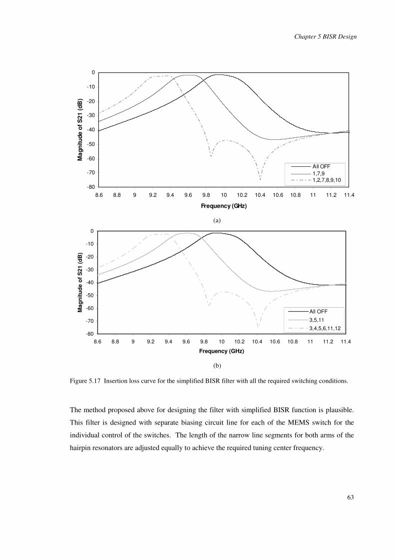
Chapter 5 BISR Design
63
-80
-70
-60
-50
-40
-30
-20
-10
0
8.6 8.8 9 9.2 9.4 9.6 9.8 10 10.2 10.4 10.6 10.8 11 11.2 11.4
Frequency (GHz)
Ma
gn
itu
de
of
S2
1 (
dB
)
All OFF
1,7,9
1,2,7,8,9,10
(a)
-80
-70
-60
-50
-40
-30
-20
-10
0
8.6 8.8 9 9.2 9.4 9.6 9.8 10 10.2 10.4 10.6 10.8 11 11.2 11.4
Frequency (GHz)
Ma
gn
itu
de
of
S2
1 (
dB
)
All OFF
3,5,11
3,4,5,6,11,12
(b)
Figure 5.17 Insertion loss curve for the simplified BISR filter with all the required switching conditions.
The method proposed above for designing the filter with simplified BISR function is plausible.
This filter is designed with separate biasing circuit line for each of the MEMS switch for the
individual control of the switches. The length of the narrow line segments for both arms of the
hairpin resonators are adjusted equally to achieve the required tuning center frequency.
Chapter 5 BISR Design
64
5.5 Limitation of the BISR Filter design
5.5.1 Filter design specific
This classification can only be used for this specific tunable filter. The findings cannot be
generalized to other tunable filter. The most important structures in this tunable filter are the
switching area and the MEMS switches. The switching areas are the narrow line segments and
the functionality of the MEMS switches. A small change in the filter design will affect the
output frequency response of the filter other than the changes on the MEMS biasing line. Hence,
any changes in the design of the filter or the MEMS switches might change the effects of the
fault on the filter. The whole process of mapping the fault and effect has to be done on the filter
with the small changes.
5.5.2 Combination of two or more faults
This analysis does not take into account the combination of two or more faults that happen on
the filter simultaneously, and also on different locations of the faulty filter. This analysis will be
able to detect the combine fault of the stuck-at-on and stuck-at-off fault only. These combined
faults have to be tested using three of the filter settings, that is, for tuning to the center frequency
of 10.0 GHz, 9.6 GHz and 9.3 GHz.
The other kind of faults such as particulate contamination, broken structures, short circuit and
parametric variations can only be properly detected if it is a single fault occurring on the filter at
one time. If the combined faults are required for this testing, a new set of combined faults
testing has to be done using the required combined faults.
5.5.3 BISR Filter has to be implemented with another external system
These BISR filters have to be implemented together with another external system that is able to
record the number of cycles that is being used by the MEMS switches. When the mean number
of the switches’ lifetime cycles has reached its limit, the redundant structures of the whole filter
will function as the main structures for tuning the filter. In addition, the main switches will be
switched off completely and will not be used from that time onwards. Hence the lifetime of the
external system has to be longer than the lifetime of the BISR filter.

Chapter 6 Conclusions and Future Works
65
Chapter 6
6. Conclusions and Future Works
6.1 Defects and Their Effects on RF Filter
The common defects on a tunable RF MEMS filter have been simulated and their effects on the
RF filter response are analyzed. The filter under investigation is a newly designed 3-pole
Chebyshev bandpass filter which switches between 9.3GHz, 9.6GHz and 10GHz. The defects
that have been analyzed in this study are:
a. gold particulate contamination
b. geometrical variation which includes broken structure and short circuit
c. MEMS switch stuck-at-ON and OFF
As expected, rather than obtaining specific faulty filter response with respect to individual
defect, different general filter performance deterioration are observed with different nature of the
defects. Therefore, rather than pinpointing the exact defects that cause the faulty response
analyzing the faulty response can help the defect identification process by narrowing down the
potential suspects. The study also enables the impact of each defect to be known, thus helping
the designer to control sensitive design / fabrication parameters.
In future, a more general fault model for the tunable filter can be developed which also take into
account overlapping multiple defects. The final aim is to provide accurate guesses to the defects
that cause the faulty filter response.

Chapter 6 Conclusions and Future Works
66
For future works, a probabilistic design as in Figure 6.1 can be used to simulate the effects of the
combination of faults on the behaviors of the device. The probabilistic design system analyzes
uncertain parameter input of a system. These input parameters are the fault from geometrical
variations (width of resonator, length of resonator, width of narrow line segment, length of
narrow line segments, width of 50 ohms feedline, and width of the gap between two resonators),
location of particulate contamination, stuck-at-on fault on switches and stuck-at-off fault on
switches. These parameters are defined as random input variables and are characterized by their
type of distribution and measurements in mean and standard deviation. The key outputs of the
simulation are defined as random output combination of several faults on the filter. With the
random output of the combined faults on the filter via Monte Carlo simulation, the most
probable occurrence combination faults will be generated together with the probability value.
This combination of faults on the filter is simulated to obtain the simulated output frequency
response. Using the list of most probable occurrence combination of faults, the measured output
frequency response can predict the possible faults on the faulty filter. The following is the
schematic diagram on the proposed working of the probabilistic design system as referred
earlier.
Figure 6.1 Schematic on the proposed working of Probabilistic Design System.

Chapter 6 Conclusions and Future Works
67
6.2 BISR Design
The second part of this work has demonstrated that the symmetries and redundancies in the filter
design bring about the possibility of a Built-In Self Repairable mechanism to be developed for
the device. To preserve the performance of the BISR filter, minor design parameters such as
length of resonator’s end, low impedance patches and feedlines location have to be retuned.
For future work, the technique should be tested on real filter with the BISR implementation for
all possible combination of switch failures. A microcontroller can be used to implement the
scheme.

68
References
[1] G. M. Rebeiz and J. B. Muldavin, “RF MEMS Switches and Switch Circuits,” IEEE
Microwave Magazine, vol. 2, no. 4, pp. 59-71, Dec. 2001.
[2] “Model 1210 analog Accelerometer,” Silicon Designs, Inc..
[Online] Available: http://www.silicondesigns.com/Pdf/1210.pdf [Accessed: June 3,
2008].
[3] A. Jain, A. Kopa, Y. Pan, G.K. Fedder, H. Xie, “A Two-Axis Electrothermal
Micromirror for Endoscopic OCT,” IEEE Journal of Selected Topics in Quantum
Electronics, vol.10, pp. 636-642, 2004.
[4] D. T. McCormick, W. Jung, Y.-C. Ahn, V. Milanovic, Z. Chen, and N. C. Tien, “A
MEMS based optical Coherence Tomography Image System and optical Biopsy Probes
for Real-Time, High Resolution In-Viva and In-Vitro 2-D or 3-D Imaging,” in
IEEE/LEOS International Conference on Optical MEMS and Their Applications
Conference, 2006, pp. 162-163.
[5] L. J. Hornbeck, “Digital Light Processing and MEMS: an overview,” IEEE/LEOS
Advanced Applications of Lasers in Materials Processing, 1996/ Broadband Optical
Networks/ Smart Pixels/ optical MEMS and Their Applications, 1996, pp. 7-8.
[6] M. Tokeshi, K. Sato, and T. Kitamori, “Integration chemistry for bio-chip: Integration of
immunoassay and bio-chemical lab on a chip,” RIKEN Review: Focused on Science and
Technology in Micro/Nano Scale, no.36, pp. 24-25, June 2001.
[7] S. Haeberle and R. Zengerle, “Microfludic platforms for lab-on-chip applications,” Lab
on a chip, July 2007, pp. 1094-1110.
69
[8] K. Kim, E. Nilsen, T. Huang, A. Kim, M. Ellis, G. Skidmore, and J.-B. Lee, “Metallic
microgripper with SU-8 adaptor and end-effectors for heterogeneous micro/nano
assembly applications,” Microsystem Technologies, vol. 10, no. 10, pp. 1432-1858,
2004.
[9] S. Ku and S.E. Salcudean, “Design and Control of a Teleoperated Microgripper for
Microsurgery,” in IEEE Proceedings of the International Conference on Robotics and
Automation, 1996, pp.1-6.
[10] R. Hochmuth, “Micropipette aspiration of living cells,” Journal of Biomechanics, vol.
33, no. 1, pp. 15-22, January 2000.
[11] J. Brank, J. Yao, M. Eberly, A. Malczewski, K. Varian, and C. Goldsmith, “RF MEMS-
based tunable filters,” International Journal of RF and Microwave Computer-Aided
Engineering, vol. 11, no. 5, pp. 276-284, 2001.
[12] A. Kolpekwar and R.D. (Shawn) Blanton, “Development of a MEMS Testing
Methodology,” in Proceedings of the 1997 IEEE International Test Conference, 1997,
pp. 923-831.
[13] A. Kolpekwar, C. Kellen, and R. D. (Shawn) Blanton, “MEMS Fault Model Generation
using CARAMEL,” in Proceedings of the 1999 IEEE International Test Conference,
1998, pp. 557-566.
[14] X. Xiong, Y.-L. Wu, and W.-B. Jone, “A Dual-Mode Built-in Self-Test Technique for
Capacitive MEMS Devices,” IEEE Transactions on instrumentation and Measurement,
vol. 54, no. 5, pp.1739-1750, Oct 2005.
[15] R. L. Borwick, P. A. Stupar, J. F. DeNatale, R. Anderson, and R. Erlandson, “Variable
MEMS capacitors implemented into RF filter systems,” IEEE Transaction Microwave
Theory and Techniques, vol. 51, no. 1, pp. 315-319, Jan 2003.

70
[16] G. M. Kraus, C. L. Goldsmith, C. D. Nordquist, and C. W. Dyck, P. S. Finnegan, F.
Austin IV, A. Muyshondt and C. T. Sullivan, “A Widely Tunable RF MEMS End-
coupled Filter,” IEEE MMT-S Digest, 2004, pp. 429-432.
[17] J. Nath, D. Ghosh, J-P, Maria, A.I. Kingon, W. Fathelbab, P.D. Franzon, and M.B.
Steer, “An Electronically Tunable Microstrip Bandpass Filter Using Thin-Film Barium-
Strontium-Titanate (BST) Varactors”, IEEE Transactions on Microwave Theory and
Techniques, vol. 53, no. 9, pp. 2707-2712, September 2005.
[18] X. Y. Zhang and Q. Xue, “Novel Centrally Loaded Resonators and Their Applications
to Bandpass Filters,” IEEE Transactions on Microwave Theory and Techniques, vol. 56,
no. 4, April 2008, pp. 913-921.
[19] C. D. Nordquist, C. L. Gold Smith, C. W. Dyck, G. M. Kraus, P. S. Finnegan, F. Austin
IV and C. T. Sullivan, “X-band RF MEMS tuned combline filter”, Electronics Letters,
vol. 41, no. 2, pp. 76-77, Jan. 2005.
[20] I.C. Reines, C.L. Goldsmith, C.D. Nordquist, C.W. Dyck, G.M. Kraus, T.A. Plut, P.S.
Finnegan, F. Austin, and C.T. Sullivan, “A low loss rf mems Ku-band integrated
switched filter bank,” IEEE Microwave and Wireless Component Letters, vol. 15, no. 2,
pp. 74-76, Feb. 2005.
[21] K. Entesari and G.M. Rebeiz, “A Differential 4-bit 6.5-10-GHz RF MEMS Tunable
Filter”, IEEE Transactions on Microwave Theory and Techniques, vol. 53, no. 3,
pp.1003-1110, March 2005.
[22] M. Sachdev, “A Realistic Defect Oriented Testability Methodology for Analog
Circuits,” Journal of Electronic Testing: Theory and Applications, vol. 6, pp. 265-276,
1995.
[23] E. Jenn, J. Arlat, M. Rimen, J. Ohlsson and J. Karlsson, “Fault Injection into VHDL
Models: The MEFISTO Tool,” in Proceedings of the Twenty-fourth International
Symposium on fault-Tolerant Computing (FTCS-24), 1994, pp. 66-75.

71
[24] F.C.M. Kuijstermans, M. Sachdev and A.P. Thijssen, “Defect-Oriented Test
Methodology for Complex Mixed-Signal Circuit,” in Proceedings of European Design
and Test Conference (ED&TC 1995), 1995, pp. 18-23.
[25] J.P, Shen, W. Maly, and F.J. Ferguson, “Inductive Fault Analysis of MOS Integrated
Circuits,” IEEE Design and Test of Computers, vol. 2, no. 6, pp. 13-26, Dec. 1985.
[26] M. J. Ohletz, “Realistic Faults Mapping Scheme for the Fault Simulation of Integrated
Analogue CMOS Circuits,” in International Test Conference, October 1996, pp. 776-
785.
[27] A. Kolpekwar, T. Jiang and R.D. (Shawn) Blanton, “CARAMEL: Contamination and
Reliability Analysis of MicroElectromechanical Layout,” Journal of
Microelectromechanical Systems, vol. 8, no. 3, pp. 309-318, 1999.
[28] T. Jiang and R.D. (Shawn) Blanton, “Particulate Failure for Surface-Micromachined
MEMS,” in Proceedings of the 1999 IEEE International Test Conference, 1999, pp.
329-337.
[29] T. Jiang, C. Kellen and R.D. (Shawn) Blanton, “Inductive Fault Analysis of a
Microresonator,” in Technical Proceedings of the 1999 International Conference of
Modeling and Simulation of Microsystems, 1999, pp. 498-501.
[30] T. Jiang and R.D. (Shawn) Blanton, “Inductive Fault Analysis of Surface-
Micromachined MEMS,” IEEE Transactions on Computer-Aided Design of Integrated
Circuits and Systems, vol. 25, no. 6, pp. 1104-1116, June 2006.
[31] N. Deb and R.D. (Shawn) Blanton, “Analysis of Failure Sources in Surface-
Micromachined MEMS,” in Proceedings of the 2000 IEEE International Test
Conference, 1999, pp. 739-749.
[32] N. Deb and R.D. (Shawn) Blanton, “High-Level fault Modeling in Surface-
Micromachined MEMS,” Analog integrated Circuits and signal Processing, vol. 29, pp.
151-158, Oct. 2001.

72
[33] M. Lubaszewki, E. F. Cota and B. Courtois, “Microsystems Testing: an Approach and
Open Problems,” in Proceedings of the 1999 Design, Automation and Test in Europe,
1998, pp. 524-528.
[34] S. Mir, B. Charlot and B. Courtois, “Extending fault-based testing to
Microelectromechanical Systems,” in Proceedings of the Fourth IEEE European Test
Workshop, 1999, pp. 64-68.
[35] S. Mir and B. Charlot, “On the Integration of Design and Test for Chip Embedding
MEMS,” IEEE Design and Test of Computers, vol. 16, no. 4, pp. 28-38, October 1999.
[36] R. Rosing, A. Richardson, A. Dorey and A. Peyton, “Test support Strategies for
MEMS,” Proceedings of Fifth International Mixed Signal Testing Workshop, 1999, pp.
345-350.
[37] R. Rosing, A. Lechner, A. Richardson and A. Dorey, “Fault simulation and modeling of
Microelectromechanical systems,” Special Feature-Intelligent Sensors: IEE Computing
and Control Engineering Journal, vol. 11, no. 5, pp. 242-250, Oct. 2000.
[38] R. Rosing, A.M. Richardson and A.P. Dorey, “A Fault Simulation Methodology for
MEMS,” in Proceedings of the Conference on Design and Test in Europe, Paris, France,
2000, pp. 476-483.
[39] R. Rosing, R. Reinchenbach and A. Richardson, “Generation of component level fault
models for MEMS,” Microelectronics Journal, vol. 33, no. 10, pp. 861-868, 2002.
[40] X. Xiong, Y.-L. Wu, and W.-B. Jone, “Design and Analysis of Self-Repairable MEMS
Accelerometer,” Proceedings of the 2005 20th ICCC International Symposium on Defect
and Fault Tolerance in VLSI Systems (DFT’05), 2005, pp. 21-29.
[41] H. T. Su, “Switchable Filter Structures Using MEMS switches,” Reported by Hieng
Tiong Su dated on 4 July 2005, EDT Centre, Department of Electronic, Electrical and
Computer Engineering, The University of Birmingham, Edgbaston, Birmingham, 2005.

73
[42] J. D. Rhodes, Theory of Electrical Filters, New York, 1976.
[43] J.-H. Park, S. Lee, J.-M. Kim, H.-T, Kim, Y. Kwon, and Y.-K. Kim, “Reconfigurable
Millimeter-Wave Filters using CPW-Based Periodic Structure with novel Multiple-
Contact MEMS Switches,” Journal of Microelectromechanical Systems, vol. 14, no. 3,
pp. 456-463, June 2005.
[44] J.-H. Park, “Fabrication and Measurements of direct contact type RF MEMS switch,”
IEICE Electronics Express, vol. 4, no. 10, pp. 319-325, 2007.
[45] EM User’s Manual ver. 11.52, Sonnet Software Inc., North Syracuse, NY, 2007.
[46] J. A. Walraven, E. I. Cole Jr., L. R. Sloan, S. Hietala, C. P. Tigges, and C. W. Dyck,
“Failure Analysis of Radio Frequency (RF) Microelectromechanical Systems (MEMS),”
Proceedings of SPIE (Reliability, Testing, and Characterization of MEMS/MOEMS),
vol. 4558, pp. 254-259, 2001.
[47] J. A. Walraven, “Failure Mechanisms in MEMS,” in International Test Conference,
Charlotte, NC, USA, September 30-October 02, 2003, pp. 808-812.
[48] W. M. V. Spengen, R. Puers, R. Mertens, and I. DeWolf, “Experimental
Characterization of stiction due to charging in RF MEMS,” International Electron
Devices Meeting Digest, 2002, pp. 901-904.

74
List of Publications
1. S. H. Wong, K. C. Lee, and H. T. Su, M. A. M. Ali, “A built-in self repairable RF
MEMS filter using redundant structures,” in IEEE International Conference on
Semiconductor Electronics, 25-27 Nov. 2008, pp. 158-160.
2. W. Wong, H. T. Su, K. C. Lee, M. A. M. Ali, B. Y. Majlis, “Performance degradation of
defective MEMS tunable RF filter,” in Asia-Pacific Conference on Applied
Electromagnetics, 4-6 Dec. 2007, pp. 1-5.
3. K. C. Lee, W. S. H. Wong, H. T. Su, “Fault Analysis of a MEMS Tuneable Bandpass
Filter,” in 5th Student Conference on Research and Development, 11-12 Dec. 2007, pp.
1-5.
4. K. C. Lee, H. T. Su, and W. S. H. Wong, “Realization of a wideband band pass filter
using cascaded lowpass to highpass filter,” in International conference on Microwave
and millimeter Wave Technology, Nanjing, China, 21-24 April 2008, pp. 14-17.