degradation effect of polymer hole transport layer on organic electroluminescence device performance
TRANSCRIPT
Degradation effect of polymer hole transport layer on organicelectroluminescence device performance
Jeong-Woo Choia,*, Joo Sung Kima, Se Yong Oha, Hee-Woo Rheea,Won Hong Leea, Sang Baek Leeb
aDepartment of Chemical Engineering, Sogang University, C.P.O. Box 1142, Seoul 100-611, South KoreabDepartment of Chemical Engineering, Cheju National University, Cheju 690-756, South Korea
Abstract
The effect of heat treatment to the polymer hole transport layer (HTL) on the performance of the organic light emitting devices (OLEDs)
was investigated. Poly-N- (p-diphenylamine) phenyl methacrylamide [PDPMA] was used as a polymer HTL. Polymer HTL was coated onto
ITO substrate by spin coating method. The effect of polymer HTL degradation on the turn-on voltage of the prepared OLEDs was
investigated by I±V measurement at the various conditions of temperature and exposure time. OLEDs were fabricated with the structure
of ITO/Polymer HTL/Emitting layer (Alq3)/Electrode (Al), and polymer HTL was treated by heat. The different surface morphologies of
polymer HTL was observed by atomic force microscopy (AFM) at the variation of exposure time and temperature. The degree of the polymer
HTL degradation was increased as the exposure time and temperature were increased, and it was observed that the increase of turn-on voltage
was primarily caused by the polymer HTL degradation. q 2000 Elsevier Science S.A. All rights reserved.
Keywords: Organic electroluminescence device; Atomic force microscopy; Thermal degradation
1. Introduction
In the electroluminescence devices industry, the remark-
able technological improvement has been made with the
initial discovery of conjugated polymer electrolumines-
cence [1,2]. It has been widely known that the polymer
light emitting diode (LED) displays have several advan-
tages, such as easiness of fabrication and commercially
useful lifetime [3], compared with the inorganic-based
LED. Polymer LED shows no image ¯icker, image latency,
and loss of contrast or color change, compared with the
monomer-based LED. For the commercialization of organic
electroluminescence devices, two major criteria should be
considered, i.e. quantum ef®ciency and lifetime. In the
viewpoint of the importance of the hole mobility and the
density in the emitting layer (EML), the number of injected
holes from the anode should be balanced to enhance the EL
quantum ef®ciency [4]. It has been considered that humidity
and Joule heat would be the crucial factors mainly affecting
the degradation process of the devices [5±7]. Although the
encapsulation method has been used as one of the best poli-
cies to protect the EL device from degradation sources and
to extend the lifetime of devices, the Joule heat caused by
large current ¯ow irrespective of light emission could not be
eliminated. Other methods to reduce the current ¯ow with-
out the reduction of the light emitting performance of the
device have also been reported, such as the fabrication of the
polymer/organic hetero-structure devices with various
organic layers for hole blocking [8]. Even though the
Joule heat can be prevented by fabricating this kind of struc-
ture, the ef®ciency of electroluminescence device can be
reduced if polymer layer degradation occurs. It has also
been reported that the poor electroluminescence ef®ciency
can be resulted from the device degradation caused by the
crystallization of the HTLs [9,10] or the delimitation at the
cathode/Alq3 interface [11,12]. However, the time course
behavior or the temperature dependency of the polymer
HTL degradation caused by the Joule heat has not been
reported yet. In this study, the degradation processes of
polymer HTL were investigated by the observation of
morphology change using atomic force microscopy
(AFM) at the different conditions of temperature and expo-
sure time. Maximum temperature in the experiment was
958C due to the consideration of local Joule heat [13]. The
effects of the surface degradation of polymer HTL on the I±
V characteristics and turn-on voltage of the fabricated elec-
troluminescence device were investigated.
Thin Solid Films 363 (2000) 271±274
0040-6090/00/$ - see front matter q 2000 Elsevier Science S.A. All rights reserved.
PII: S0040-6090(99)01001-9
www.elsevier.com/locate/tsf
* Corresponding author. Tel.: 1 82-2-705-8480; fax: 1 82-2-711-0439.
E-mail address: [email protected] (J.-W. Choi)
2. Experimental
Tris(8-quinolinolato)aluminum (Alq3), used as light-
emitting material, was purchased from Sigma (St. Louis,
USA). Poly-N-(p-diphenylamine) phenyl methacrylamide
[PDPMA] was synthesized and used as a polymer HTL
[14]. The OLED consist of ITO/HTL (polymer)/EML
(Alq3)/Electrode (Al). The ITO-coated glass plates were
kindly obtained from Samsung Display Device Co.
(Korea). The ITO-coated glass (transparent anode, sheet
resistance ,20 V/cm2) was treated by chromic-sulfuric
acid solution followed by rinsing with de-ionized water,
methanol, and acetone, and ®nally dried under nitrogen
gas. ITO-coated glass was treated with O2 plasma treatment.
The polymer HTL was prepared onto the pretreated ITO
glass by spin coating method (PWM32, Headway Research
Co., USA). The thickness of polymer HTL was found as
about 800 AÊ based on the measurement by the ellipsometry
analysis. Each polymer HTL prepared onto ITO glass was
thermally treated at 55 and 958C, respectively. The exposure
times to temperature variation were 3, 5, 7 and 14 days,
respectively. The surface morphologies of the thermally
treated polymer HTL according to the variation of exposure
time and temperature were obtained by AFM (Autoprobe
CP, Park Scienti®c Instruments, USA). The Alq3 (EML) and
aluminum electrode were then sequentially deposited onto
polymer HTL by vacuum evaporation (1026 Torr). The
thickness of Alq3 emitting layer and of Al to be deposited
were set to 800 and 1000 AÊ , respectively (CRTM-5000,
SINKU-KIKO Co., Japan). The I±V characteristics of the
fabricated device were measured using the source measur-
ing unit (SMU 236, Keithley, USA).
3. Results and discussion
Since the ITO surface was used as a template for the
J.-W. Choi et al. / Thin Solid Films 363 (2000) 271±274272
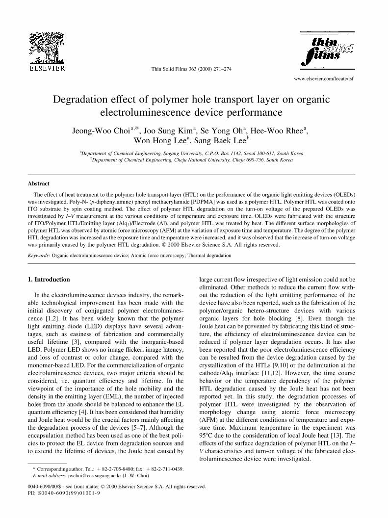
Fig. 1. The PDPMA morphology after 3 days (at 258C).
Fig. 2. The PDPMA morphology after 14 days (at 258C).
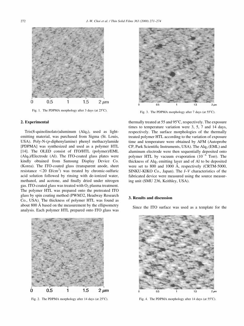
Fig. 3. The PDPMA morphology after 7 days (at 558C).
Fig. 4. The PDPMA morphology after 14 days (at 558C).
polymer HTL deposition and the surface morphology of the
polymer HTL can be affected by the template morphology,
the ITO surface morphology could be a very important
factor to affect the effective interface contact and effective
hole transport. O2 plasma treatment leads to improvement of
uniformity of the ITO surface, and thereby increases the
effective interfacial area. The change of the polymer HTL
morphology would be affected mainly by the thermal treat-
ment, not by the change of the template morphology.
Because, the severe changes of the template (ITO) morphol-
ogy was not be observed with respect to the various condi-
tions of time and temperature.
The surface morphologies of PDPMA ®lms fabricated by
spin coating method at the various temperature and exposure
time were shown in Figs. 1±6. It was observed that the thin
layer of PDPMA showed a fairly good surface morphology
and its surface morphology was not changed with the expo-
sure time at room temperature (258C) (Figs. 1 and 2). In the
case of the PDPMA ®lms treated at 558C, the quality of
surface morphology became worse than those treated at
room temperature in Figs. 3 and 4. There was not a remark-
able change in the surface morphology until 5 days, but the
number of voids (dark spots) was increased and the size
became broaden from 7 days. From Figs. 5 and 6. it was
observed that the trend in morphology degradation at 958Cwas similar to that at 558C except that the remarkable degra-
dation occurred from 5 days. In order to elucidate the rela-
tionship between the degradation of PDPMA morphology
and device performance, the I±V characteristics of the
devices fabricated at different conditions were also investi-
gated. In Figs. 3±8, bounces were observed in the I±V curves.
These irregularities should be related with the thermal treat-
ment conditions such as the variation of time and tempera-
ture. Since the degradation of the polymer HTL would result
J.-W. Choi et al. / Thin Solid Films 363 (2000) 271±274 273
Fig. 5. The PDPMA morphology after 5 days (at 958C). Fig. 6. The PDPMA morphology after 14 days (at 958C).
Fig. 7. The I±V Characteristic of ITO/PDPMA(PHTL)/Alq3(EML)/Al with time (at 558C): (X), ®rst; (W), 7 days; (P), 14 days; (L) 21 days).
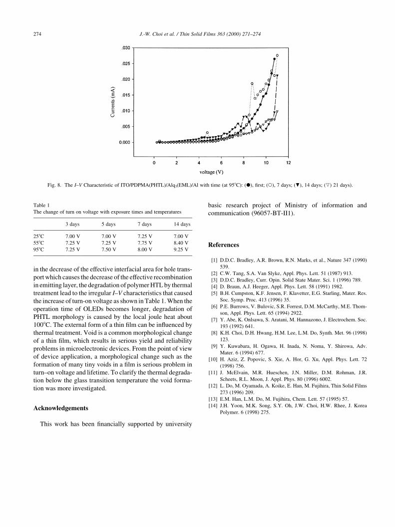
in the decrease of the effective interfacial area for hole trans-
port which causes the decrease of the effective recombination
in emitting layer, the degradation of polymer HTL by thermal
treatment lead to the irregular I±V characteristics that caused
the increase of turn-on voltage as shown in Table 1. When the
operation time of OLEDs becomes longer, degradation of
PHTL morphology is caused by the local joule heat about
1008C. The external form of a thin ®lm can be in¯uenced by
thermal treatment. Void is a common morphological change
of a thin ®lm, which results in serious yield and reliability
problems in microelectronic devices. From the point of view
of device application, a morphological change such as the
formation of many tiny voids in a ®lm is serious problem in
turn±on voltage and lifetime. To clarify the thermal degrada-
tion below the glass transition temperature the void forma-
tion was more investigated.
Acknowledgements
This work has been ®nancially supported by university
basic research project of Ministry of information and
communication (96057-BT-II1).
References
[1] D.D.C. Bradley, A.R. Brown, R.N. Marks, et al., Nature 347 (1990)
539.
[2] C.W. Tang, S.A. Van Slyke, Appl. Phys. Lett. 51 (1987) 913.
[3] D.D.C. Bradley, Curr. Opin. Solid State Mater. Sci. 1 (1996) 789.
[4] D. Braun, A.J. Heeger, Appl. Phys. Lett. 58 (1991) 1982.
[5] B.H. Cumpston, K.F. Jensen, F. Klavetter, E.G. Starling, Mater. Res.
Soc. Symp. Proc. 413 (1996) 35.
[6] P.E. Burrows, V. Bulovic, S.R. Forrest, D.M. McCarthy, M.E. Thom-
son, Appl. Phys. Lett. 65 (1994) 2922.
[7] Y. Abe, K. Onlsawa, S. Aratani, M. Hannazono, J. Electrochem. Soc.
193 (1992) 641.
[8] K.H. Choi, D.H. Hwang, H.M. Lee, L.M. Do, Synth. Met. 96 (1998)
123.
[9] Y. Kuwabara, H. Ogawa, H. Inada, N. Noma, Y. Shirowa, Adv.
Mater. 6 (1994) 677.
[10] H. Aziz, Z. Popovic, S. Xie, A. Hor, G. Xu, Appl. Phys. Lett. 72
(1998) 756.
[11] J. McElvain, M.R. Hueschen, J.N. Miller, D.M. Rohman, J.R.
Scheets, R.L. Moon, J. Appl. Phys. 80 (1996) 6002.
[12] L. Do, M. Oyamada, A. Koike, E. Han, M. Fujihira, Thin Solid Films
273 (1996) 209.
[13] E.M. Han, L.M. Do, M. Fujihira, Chem. Lett. 57 (1995) 57.
[14] J.H. Yoon, M.K. Song, S.Y. Oh, J.W. Choi, H.W. Rhee, J. Korea
Polymer. 6 (1998) 275.
J.-W. Choi et al. / Thin Solid Films 363 (2000) 271±274274
Fig. 8. The I±V Characteristic of ITO/PDPMA(PHTL)/Alq3(EML)/Al with time (at 958C): (X), ®rst; (W), 7 days; (P), 14 days; (L) 21 days).
Table 1
The change of turn on voltage with exposure times and temperatures
3 days 5 days 7 days 14 days
258C 7.00 V 7.00 V 7.25 V 7.00 V
558C 7.25 V 7.25 V 7.75 V 8.40 V
958C 7.25 V 7.50 V 8.00 V 9.25 V