deliverable 2 - timewarp it consulting gmbh · 1.3 deliverable objective ... figure 20: elektor...
TRANSCRIPT
1
DELIVERABLE 2.2
Report on the impact of emerging micro- and
nanotechnologies on waste prevention
Grant Agreement number: 226752
Project acronym: ZEROWIN
Project title: Towards Zero Waste in Industrial Networks
FUNDING Scheme: Collaborative project
Delivery date: 31st Mai 2012
Deliverable number: 2.2
Work package number: 2
Lead participant: Technical University of Berlin (TU-Berlin)
Nature: Research
Dissemination level: Public
Author(s): Dr.-Ing. Andreas Middendorf, Dr. Stewart Hickey, Dr. Bernd Kopacek, Sabine Schadlbauer
Project coordinator: Dr. Bernd Kopacek, Austrian Society for Systems Engineering and Automation
Tel: +43-1-298 20 20
Fax: +43-1-876 06 619
E-mail: [email protected]
Project website: www.zeroWIN.eu

2
TABLE OF CONTENTS
TABLE OF CONTENTS ......................................................................................................... 2
LIST OF FIGURES .................................................................................................................. 3
EXECUTIVE SUMMARY ...................................................................................................... 4
1. INTRODUCTION ................................................................................................................ 5
1.1 Background ............................................................................................................................. 5
1.2 ELIMA ...................................................................................................................................... 5
1.3 Deliverable Objective ............................................................................................................. 6
1.4 Deliverable Scope .................................................................................................................. 6
1.5 Deliverable Restrictions ........................................................................................................ 7
1.6 Deliverable Structure ............................................................................................................. 7
2. INFORMATION FLOW IN ZEROWIN NETWORK .................................................... 8
2.1 Information context in reuse management ......................................................................... 8
2.2 Information Flow ..................................................................................................................... 9
2.3 Challenges and Requirements on information based reuse in industrial networks ... 10
2.4 Challenges and Requirements on information based on EOL ...................................... 12
2.5 Challenges and Requirements on information based technical concepts .................. 12
2.6 Considerations for EOL data generated by the proposed condition Monitoring
Technologies ............................................................................................................................... 14
3. TECHNOLOGY CONCEPTS FOR REUSE .................................................................. 16
3.1 Introduction ........................................................................................................................... 16
3.2 Condition Monitoring Technologies Development .......................................................... 16
3.3 PC Condition Monitoring ..................................................................................................... 24
3.4 Concepts based on programmable logic to enable reuse of products ........................ 51
3.5 Evaluation of EOL levels according to the technology concepts .................................. 58
4. SUMMARY ..................................................................................................................... 58
5. REFERENCES ................................................................................................................ 61
6. GLOSSARY OF SYMBOLS AND ABBREVIATIONS ............................................. 63

3
LIST OF FIGURES Figure 1: ZeroWIN Scope & Boundary .................................................................................. 6
Figure 2: Conceptual information tracking of inputs and products .......................................... 9
Figure 3: Material and products cycle ...................................................................................10
Figure 4: ROI for condition based maintenance affords ........................................................13
Figure 5: Platform for intelligent condition monitoring ...........................................................17
Figure 6: Chip Embedding development ...............................................................................17
Figure 7: Communication concept in the modular structure ..................................................18
Figure 8: The circuit diagram for the master sheet ................................................................19
Figure 9: Energy Harvesting – Currently available technologies and future challenges ........20
Figure 10: Energy-autarkic Condition Monitoring System for a paper mill .............................20
Figure 11: Open IGBT-Module .............................................................................................22
Figure 12: Collector-emitter-voltage VCE versus temperature ................................................22
Figure 13: thermal behaviour within a new (blue curve) and aged (red curve) power module .............................................................................................................................................24
Figure 14: VCE versus number of disconnected wire bonds and chips at load current ...........24
Figure 15: Condition Monitoring for PC Systems ..................................................................25
Figure 16: Results of period and mean temperature analysis ...............................................29
Figure 17: Results of temperature swing versus mean temperature analysis .......................29
Figure 18: Block diagram of data storage methodology ........................................................30
Figure 19: Log file size with data reduction verses no data reduction ...................................30
Figure 20: ELEKTOR RFID reader .......................................................................................31
Figure 21: RFID Circuit .........................................................................................................32
Figure 22: ISO 14443 definition for "pause" in communication .............................................33
Figure 23: Possible bit sequences at output of microcontroller .............................................36
Figure 24: Flow diagram outlining operation of transmission section of assembly code ........37
Figure 25: Flow chart for receiving and decoding of data ......................................................39
Figure 26: AVR Studio 5 debugging interface .......................................................................42
Figure 27: Layout of stimulus file for AVR Studio 4 ...............................................................43
Figure 28: PICC output sequences with delays highlighted for stimulus file generation ........44
Figure 29: Example of input and output calculations for stimulus files ..................................45
Figure 30: CRC generation and testing software ..................................................................45
Figure 31: Sample of graphed output of log file from AVR Studio 4 ......................................46
Figure 32: RFID Communications Module with Antenna .......................................................47
Figure 33: REQA required by the PICC ................................................................................47
Figure 34: Output of the RFID antennae and corresponding comparator output ...................48
Figure 35: REQA ..................................................................................................................48
Figure 368: Period of the modulation ....................................................................................48
Figure 379: Signal response from tag as measured at the reader ........................................49
Figure 38: PCI Circuitry ........................................................................................................50
Figure 39: Role of PC Condition Monitoring Concept in ZeroWIN’s Resource Exchange Platform ................................................................................................................................50
Figure 40: Eco-design Methodology for Enabling Industrial Networking of Electronic Products and Assemblies ....................................................................................................................51
Figure 41: The Bathtub Curve ..............................................................................................52
Figure 42: Programmable Device Types...............................................................................53
Figure 43: PLD Configuration Methods .................................................................................54
Figure 44: Internal structure of a CPLD. ...............................................................................55
Figure 45: Internal structure of a FPGA ................................................................................55
Figure 46: CMOS logic configuration for aircraft ...................................................................57
Figure 47: Replacement for CMOS logic configuration for aircraft ........................................57

4
EXECUTIVE SUMMARY The hypothesis that waste is material that is useless and unwanted because no information and knowledge about it is available, has been introduced and suggested in this report. Based on this hypothesis technical concepts have been suggested. A modular hardware concept based on embedding of passive and active components in various stacks with standardized communication protocol between the different stacks has the potential to fulfill variable demands from several case studies. The Implementation of various energy harvesters to create autonomous micro systems enables in combination with wireless network communication the monitoring of sensor data in harsh environments and on difficult to reach places. IGBT (insulated gate bipolar transistor) are the back bone of modern power electronics. The condition monitoring of such devices is crucial for all energy infrastructures now and in the future. A concept for the photovoltaic industry is developed together with the Zerowin partner TTA and will be implemented and tested in the next time. Computer condition monitoring utilising existing hardware sensing technologies within systems is demonstrated at a proof of concept level. This is applicable CS1 and CS3 in ZeroWIN. The system utilises thermal sensors already present in the components of a computer system to track the health of the computer throughout its lifetime. At end of life (EOL), this data can be extracted using radio frequency identification (RFID) to allow a fast first diagnosis of the reuse potential of the system. The choice of RFID as a suitable technology, the requirements of the MIFARE RFID standard, and the modifications made to the standard to allow the transmission of the volumes of data required for lifetime condition monitoring is investigated. Programmable logic devices (PLDs) are a technology that is eminently suitable to increase reuse in industrial networks. When utilising PLD technology, the internal hardware configuration (circuit) is changed rather than the external printed circuit board (PCB) design. It is described how a modular card containing a state-of-the-art PLD can be used in various generations of a product or in a completely different application. This has the benefits in that the PCB only needs to be designed and manufactured once and when the design is to be upgraded or the functionality changed, then the configuration of the PLD is changed via a software program running on a programmer PC.

5
1. INTRODUCTION
1.1 Background
This deliverable follows the hypothesis that waste is material without sufficient related knowledge. Knowledge in this context refers to information regarding material quantity, quality, ageing and handling. Waste can only be used as an input for industrial processes if specific details and information regarding its state is readily available. This new hypothesis allows industrial partners to view waste as a material resource or product rather than waste. In a production context, increasing the availability of explicit and implicit information about materials from the manufacturer(s) involved creates the opportunity for other manufacturers to use these materials as inputs for their respective production processes. This information could comprise of static and dynamic data (e.g. Bill of materials (BoM), remaining residual life etc.) specifically related to the secondary production resources (by-products) but also spatially referenced data (e.g. location information). Information pertaining to production resources includes:
� End of life estimation � History and ingredients � Material condition and contamination � Actual geographic position � Amount and weight � Handling and Transportation
Making information readily available regarding the current state of materials/by-products aims to achieve environmentally and economically and even socially positive cultural effects. This new hypothesis will serve to enhance materials management and deliver a means to prevent waste occurring in the primary instance. From the European Union (EU) Directive 2002/96/EC, it must also be taken into consideration that reuse of secondary production resources (by-products) has, with respect to its counterpart of recovery (recycling), legal implications. The proposed hypothesis can make it simple for stakeholders to determine whether their practices comply with this legal obligation.
1.2 ELIMA
The is deliverable builds specifically on the findings of the previous FP-project “ELIMA - Environmental Life Cycle Information Management and Acquisition for Consumer products” where the feasibility of advanced concepts in managing the life cycle of products has been tested in 2 real-life cases – one refrigerator and a game console. The principle behind ELIMA is that the manufacturer of a product should, in taking extended producer responsibility, have data available on all stages of the product life cycle. This calls for an integrated information system, with databases and management tools under the control of the manufacturer, but open to access by other parties such as those involved in supply of components, the maintenance and the recycling of the product. It is this information system that the project will prototype for two typical cases. The rapidly changing nature of information technologies means that ELIMA systems must be robust and flexible; if well designed it can exploit emerging technologies to bring the manufacture, component supplier, user and recycler together as a unit. The ELIMA system combines so called static environmental data programmed in at the manufacturing stage e.g. materials used, together with dynamic data acquired from sensors active throughout the life cycle of the product. Therefore, future consumer product systems

6
will need memory for data storage and systems that record data to monitor environmental parameters such as time, temperature, shock or vibration. This basis has been developed further in this deliverable.
1.3 Deliverable Objective
The deliverable aims to develop new technology concepts to overcome the lack of information associated with resources/by-products of the production process. The use of waste as a raw material input for processes is a concept which is ever omnipresent in the natural world. The overall objective here is to realize this concept in the industrial domain and more specifically facilitate the creation of industrial networks which can metabolize unused resources occurring as a result of the production process. However, the obtaining information regarding materials/by-products requires the appropriate enabling technologies. This report discusses available technologies which can support reuse concepts in industry today and furthermore the technology solutions necessary to satisfy industrial networking into the future. The focus will be the four sectors engaged in the ZeroWIN project and more specifically the electrical and electronic (EEE), photovoltaic (PV), automotive and construction sectors.
1.4 Deliverable Scope
The report will establish the informational requirements and identify the technological solutions to tackle the hypothesis that waste is material without sufficient knowledge. Knowledge in this context refers to information regarding material quantity, quality, ageing and handling. The scope of the report will consider the players shown in Figure 1. The participating stakeholders include:
� Material suppliers
� Manufacturer
� Component Suppliers
� Recycler
� Refurbishers and dismantlers
Figure 1: ZeroWIN Scope & Boundary

7
The consumers are not addressed within this project. Electronic market places like “ebay” foster the development of “prosumers” (consumer and producer). They look for products with special properties that enable the possibility to sell the product several times. The authors expect that the implementation of life cycle units has the potential to be a relevant attribute for products according to the demands of “prosumers” in the future.
1.5 Deliverable Restrictions
The technical concepts will be introduced based on the hypothesis that waste is material without sufficient knowledge. The deliverable will focus on technical concepts and technologies that serve to industrial networking in the respective case studies introduced in Deliverable 6A1. The aim will be the improvement of reuse strategies for industrial networks. The following technical solutions will be considered:
� Tracking systems to follow the material flow from secondary resource/ by-product conception to the recycling/reuse stage
� Communication technologies to facilitate smooth informational flows between network institutions prior to the actual business transactions.
� Condition monitoring of the processing unit and also the materials production unit. These technological interventions can serve to avoid the production of off-spec products and minimize raw material use also the need for spare parts
1.6 Deliverable Structure
The deliverable is structured as follows. Chapter 2 commences with a conceptual overview of information flows in the ZeroWIN network. This includes a discussion of information in reuse management, information flow between industrial network partners, challenges and requirements of information based reuse in industrial networks, and challenges and requirements on information based technical concepts. Chapter 3 develops novel technology concepts to enable reuse of products. The developed concepts concern quality control (e.g through condition monitoring), adaptation of software tools, technology developments tackling the products’ weak point and facilitating upgrade of electronic hardware through programmable logic with built in redundancy. Finally, Chapter 4 presents a summary from the research carried out in the deliverable.
8
2. INFORMATION FLOW IN ZEROWIN NETWORK
2.1 Information context in reuse management
A major objective of this work is to increase information availability related to materials, products and by-products in industrial networks. The following technical aspects need to be considered:
� Semi-automatic saving of information in material flow � Gaining material/by-product related information at source � Information repository for storage of information � Internal communication of information between the source and the repository � External secure communication of information to industrial partners � Technical solutions for information saving, recognition and tracking
As a primary step, the information related to secondary production resources (by-products) must to be documented and saved. This step requires human intervention and therefore can only be achieved in a semi-automatic manner. Technical concepts and solutions can be put in place to perform this task. The information repository plays an important role in saving related information in central accessible place. Gaining material/by-product related information at the source considers the output of by-products in one process step inside a network institution, and also the output of components or product at the end of pipe in the value chain. Collecting and maintaining information about materials and by-products at the source can be achieved by the use of technical instruments. Recognition of materials at source follows the concept of divide and role. This step simplifies further steps in reuse of by-products. The information collection at this level can be only done in semi-automatic manner as manual intervention cannot be avoided. The information collected must be communicated internally. The use of technical instruments can speed up the time efforts. Understanding how information is communicated requires a distinction between two types of information: (1) explicit information and (2) implicit information or know-how (Grant, 2010). Explicit information is information related to the product or by-products in one process step inside a network institution, and information related to the output of components or product at the end of pipe in the value chain. Examples of explicit information include material condition, amount, weight, ingredients and history. Implicit information is information or know-how related to the actual situation or context, for example problem solving skills, coordination, which can get things done and development issues of products and components at the end of value chain. If implicit information is unavailable it is highly probable that valuable by-products of the production process will be deemed as waste. Informational requirements must also to be considered during transport between industrial network partners. Technical solutions must also consider this aspect in the network and deliver automatic tracking and localization capabilities. The understanding of information context and the use of information revolution has dramatically reduced the cost and manual efforts of the communication platforms. To ensure a correct use of information, all the introduced aspects should go through the following steps: Information identification, assessment, barrier removal, commercialization and adaptive management and documentation, review and publication.

9
2.2 Information Flow
Accounting for the information flow reflects the need to maintain information concerning materials and products inside one value chain and also to allow cross linking between other network partners. The hypothesis that waste is material without value because no information and knowledge about it is available can only be supported when the exact need of information in the industrial flow of materials is specified. Figure 2 illustrates the conceptual flow:
Figure 2: Conceptual information tracking of inputs and products Each step in the flow diagram has information requirements so that reuse management can be supported. Without catering for information requirements during each step there will be no possibilities to choose a suitable technical concept to enable the reuse of the created waste.
Procurement of materials
Utilization of materials
Accumulation of waste at source
On-site reuse
management
Off-site reuse management
Discharges and emissions
Quality and reliability
check

10
Each step should be analyzed so that the hypothesis behind this deliverable can be a solution for the reuse management inside the industrial network. Furthermore, there are information requirements when products have been used already. The product lifecycle is illustrated in Figure 3. The information requirements consider the lifecycle steps: Transport, Production, Use and End-of-life. In general, the information requirements in the suggested flow include the availability of the following facts:
� Material type, source and condition � Amount � Quality level � End-of-life estimation � Assembling and disassembling information
Figure 3: Material and products cycle
2.3 Challenges and Requirements on information based reuse in industrial
networks
Information concerning unused production resources or by-products must be of sufficient resolution before the materials concerned may be considered for the purpose of reuse for other industrial processes in other industry sectors. The fact that each industrial application has a specific production line and material specification requirement makes this issue extremely complex. Because of the multitude of different possibilities on material specifications in industry, there is seldom one single technical solution that satisfies multiple industrial partners. The sources of the requirements vary based on the industrial characterization. This is one of the reasons why information about the context is extremely important. It will help to understand the necessity of information flow and explicit and implicit information in reuse technology management. Reuse could be a viable way of improving industrial sustainability, but also a method to meet a variety of following challenges: Regulation aspects: This has always been improved based on the technical state of the art. The Rio Declaration on Environment and Development in 1992 made efforts and works on increased sustainability clear. National and international conferences and regulations have been established to ensure reuse. It is necessary for a manufacturing plant to treat its outputs when it violates criteria and standards established by governmental regulatory agencies.

11
Information Technology improvement: Information and communication technology (ICT) is subject to Continuous Improvement Process (CIP). This improvement gives the possibility to have the new thinking approach concerning reuse. The improvement can be used to establish networks between firms to exchange unnecessary output materials and by-products. The degree of success requires high innovation by constantly developing new ideas based on the state of the art of available technology. Possibility of having bilateral Reuse Interfaces: There is always a dynamic interaction in industrial networks, especially between those in the same regions. This point considers the technical interfaces and business to business interfaces. Competitive pressures and globalization: Due to globalization and opened international markets in the industrial field, there is an increased need to be at the forefront of knowledge. The reuse demand can be seen as a feature which gives the product and producer increased acceptance by the end user. Cost minimization: Production costs in all industries comprise the three components: Operation, Maintenance and Materials. Reuse causes cost savings. This will lead to cheaper production. Environmental issues: The fragile and limited environment is rapidly approaching the breaking point. No longer can industry discharge any amount of contaminants into the surrounding air, water and land without some adverse effects. This fact makes clear, that Environmental issues should be considered in line with reuse demand. Industrial specification and end user requirements: Environmental awareness has increased. This leads to changes in production requirements. Management rules and standards have been developed to ensure the end user’s needs. The end user can make an effort not to trash his purchased product when he knows that it can potentially be reused. Reuse in industrial networks assumes different facts. These facts need to be clarified. Information based reuse assumes the following aspects:
� Clearly defined technical input-output correlation between different processes (M. Chertow, 2007)
� Clear economic feasibility (ideally balanced between participating companies) (Noel Brings Jacobsen, 2007)
� Low or only moderate capital expenditure requirements � Expected long-term environmental benefits � The geographical target area � Industrial Reuse desires "social engineering" equally as "technical engineering" � Organizational stability
Operational stability (stable and larger amounts of exchangeable material or excess energy) The type of related information plays an important role in the reuse debate. Which type of information is important to enhance the reuse in industrial networks? The study of types of information forms the basic building block for the selection of appropriate technological concepts. The following information types have been selected:
� Material or product type � acceptable and unacceptable levels of contamination � acceptable and unacceptable levels of damage � quantities accepted � transportation requirements � required documentation including output tracking forms � sorting and handling requirements for each material type � Dismantling design and information � Reliability and quality � End of life estimation

12
� History and ingredients � Amount and weight
The life cycle of the by-product and controlled outputs after the accruement has to be seen as an important requirement and should be considered. Main points will be focused on output at source. The industry always faces the challenge of reducing unnecessary outputs. The benefits always remain the same:
� Cost savings � Compliance � Risk reduction � Market positioning
Production outputs can have positive or negative effects. The effect is negative when there is no more use for the outputs and it has to be landfilled. The positive effect is the aim for sustainable product development. It describes the target that unnecessary outputs in one production cycle can be used as a raw material for other process. In this case it does not matter whether the other process is inside or outside one company. The technical possibilities will make sense for a network and possible partnerships. There are requirements which have to be considered by the output material of one process step. The following requirements will be considered:
� Communication of output material in a process chain and inside the manufacturer (internal communication)
� Reducing manual efforts � Communication of the output material for other manufacturer (external
communication) � Recording the material amount � Collecting the material at source � Identification of the material and documentation of their characteristic � Tracking of the material
The selection of an appropriate technology must meet these requirements. The technological development shouldn’t be an obstacle to enhance reuse. These information requirements should be a guidance document. The technological concepts should be able to adapt new requirements in a flexible way and without much effort.
2.4 Challenges and Requirements on information based on EOL
End of life systems (EOL) includes collection, transportation, data elaboration, material flows, handling/processing and the management of these steps. The overall look to European legislation (RoHS, WEEE, ERP) demands the setting of priorities according to reuse of products as the best level followed by the reuse and recycling of materials. These requirements demands as one consequence mainly an adequate handling of information during the different EOL steps and interact strongly with the discussed technical solutions. A further aspect is the economic boundary. Collection, handling and storage of data have a significant prize. The range starts with a minimum of 100 Euro. Based on this all EOL activities have to take this into account.
2.5 Challenges and Requirements on information based technical concepts
The objective of using technical concepts in reuse materials can be summarized in the following points:
� Collection and transport should be monitored � Human health risks should be minimized

13
� Environmental issues should be automatically considered
Today’s technology provides industry with the ability to process large amounts of information and to do so in a way which presents the information in a clear and concise manner. Anticipated benefits of implementing an information technology system include increased productivity, improved profit performance and also a higher degree of information accuracy within the environment.
Figure 4: ROI for condition based maintenance affords
One of the biggest arguments against the adoption of modern technology in industry is the high costs associated with deployment. This argument will always arise when technical concepts are to be employed in a reuse strategy. But it is an undeniable fact that technology has helped the industry make many tasks easier. The rationale behind the use of technical solutions in reuse strategy is based on many reasons. One reason is the efficiency and accuracy of manual labor through man power alone which cannot be compared to that of technology. Technology improvements lead to time and cost savings. The ability of automatic and synchronized approaches of technical instruments is another reason why reuse cannot only be achieved by man power alone. Technology use in developing a reuse strategy of by-products and unnecessary output materials has different benefits. These benefits can be summarized as follows:
� Automatic recognition of the output � Dynamic and fast information flow between firms � Stand-alone application without the need of huge man power � High reliability and quality � Reliable and secure communication � Adjustable depending on user needs � Reducing the production of off-spec products � Improving production quality by reliability improvement of production equipment and
machines � Integration of different technology concepts to reach the optimal solution � Improving image and product quality

14
� Improving the competitive environment � Reducing manual labor to a minimum
Qualifying certain technical solutions and disqualifying others for the reuse strategy can be based on the following aspects:
� The technology should be upgradable. Requirements can change and the technology chosen should able to adapt to these changes.
� The technology chosen should provide return on investment. � The correct use of the technology should be well documented � The feature of cross-platform should be considered � Procurement cost should be calculable � The technology should be user friendly so that users can be trained in short time
2.6 Considerations for EOL data generated by the proposed condition Monitor-
ing Technologies
End of life data generated by the technology concepts proposed must finally be integrated into the whole EOL system and made available through the resource exchange platform. The following paragraphs outline considerations for storage and management of EOL data. Resource ─ For the condition monitoring technology concepts proposed in Section 3.2 and 3.3, the data resource for EOL data must be designed in such a manner to permit seamless capture of EOL data, and allow EOL data to be quickly converted to information so electronic parts/sub-assembles so can be used for resource exchange. ZeroWIN Deliverable 2.1 de-scribed the potential role of the EPC global architecture in conjunction with the resource ex-change platform for lifecycle data and information management for the EEE sector (Hickey et al, 2012). However, currently EPC global only supports the storage of static and quasi-static data such as object identifier, location, business step, etc. and has no support for managing sensor data. With the proposed integration of condition monitoring technologies in EEE products as well, it would be beneficial to see support for sensor data becoming part of the EPC global framework of standards. Standards development could potentially be based on the architecture developed by the European FP6 Project PROMISE. Access ─ Many enterprises find themselves with copious amounts of data residing in data-bases developed for individual business tasks with little coordination in hardware software and data modelling approaches. The challenge for ZeroWIN concerning EOL data generated by condition monitoring technologies is to not make the same mistakes, and facilitate ease of access to all members of the industrial network. Pursuing standards’ based protocols from the onset can facilitate inter-operability as industrial network deployments scale up. The EPC global architectural approach with integrated support for sensor data deployed in conjunction with the resource exchange platform can again satisfy access solution requirements Quantity ─ the notion of “Big data‟ is another challenge associated with the deployment of the proposed condition monitoring technologies for industrial networks. Big data is defined as data sets whose size is beyond the ability of typical database software tools to capture, store, manage and analyse (McKinsey and Company 2011). When there is too much EOL data of little of no value the richness of data becomes lost. Management of redundant data is anoth-er issue that must be addressed. For example, in the context of the PC monitoring technolo-gy concept, there must be mechanisms in place to deal with EOL data that is no longer needed. When computer systems (or computer parts) deemed unsuitable for refurbishment are subsequently disassembled into their separate WEEE fractions, the EOL data records associated with the previously functioning systems and parts must be retired. Quality is an equally important issue. Data streaming into EOL databases needs to be accurate. Other-

15
wise the garbage-in garbage-out (GIGO) phenomenon is probable decreasing the probability of potential resource exchange as a result. Security─ Security of data resources is another aspect closely linked with quality. If there are breaches in security, quality of EOL data is unquestionably affected. It is vital that ZeroWIN put in place safeguards against preventing unauthorised access and unplanned destruction of EOL data resources. The resource exchange platform has an obligation to suppliers and customers to keep data private or confidential from actors residing outside the industrial network. References Hickey et al, (2011) Feasibility study on technologies to facilitate product identification for various IPR models & a technology roadmap for RFID in waste management ZeroWIN De-liverable 2.1 Submitted 6th Oct 2011 McKinsey & Company (2011), “Big Data: The next frontier for innovation, competition and productivity”, The McKinsey Global Institute, June 2011.
16
3. TECHNOLOGY CONCEPTS FOR REUSE
3.1 Introduction
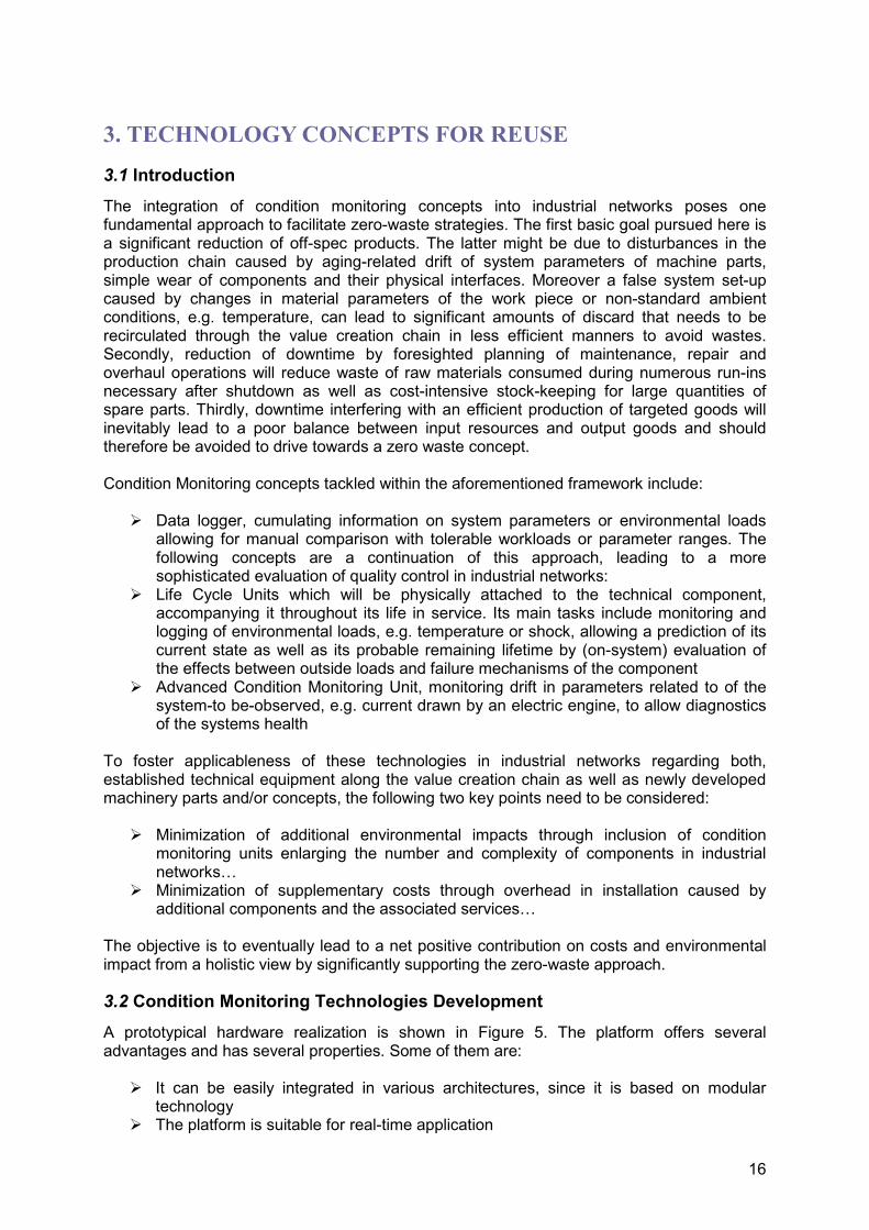
The integration of condition monitoring concepts into industrial networks poses one fundamental approach to facilitate zero-waste strategies. The first basic goal pursued here is a significant reduction of off-spec products. The latter might be due to disturbances in the production chain caused by aging-related drift of system parameters of machine parts, simple wear of components and their physical interfaces. Moreover a false system set-up caused by changes in material parameters of the work piece or non-standard ambient conditions, e.g. temperature, can lead to significant amounts of discard that needs to be recirculated through the value creation chain in less efficient manners to avoid wastes. Secondly, reduction of downtime by foresighted planning of maintenance, repair and overhaul operations will reduce waste of raw materials consumed during numerous run-ins necessary after shutdown as well as cost-intensive stock-keeping for large quantities of spare parts. Thirdly, downtime interfering with an efficient production of targeted goods will inevitably lead to a poor balance between input resources and output goods and should therefore be avoided to drive towards a zero waste concept. Condition Monitoring concepts tackled within the aforementioned framework include:
� Data logger, cumulating information on system parameters or environmental loads allowing for manual comparison with tolerable workloads or parameter ranges. The following concepts are a continuation of this approach, leading to a more sophisticated evaluation of quality control in industrial networks:
� Life Cycle Units which will be physically attached to the technical component, accompanying it throughout its life in service. Its main tasks include monitoring and logging of environmental loads, e.g. temperature or shock, allowing a prediction of its current state as well as its probable remaining lifetime by (on-system) evaluation of the effects between outside loads and failure mechanisms of the component
� Advanced Condition Monitoring Unit, monitoring drift in parameters related to of the system-to be-observed, e.g. current drawn by an electric engine, to allow diagnostics of the systems health
To foster applicableness of these technologies in industrial networks regarding both, established technical equipment along the value creation chain as well as newly developed machinery parts and/or concepts, the following two key points need to be considered:
� Minimization of additional environmental impacts through inclusion of condition monitoring units enlarging the number and complexity of components in industrial networksN
� Minimization of supplementary costs through overhead in installation caused by additional components and the associated servicesN
The objective is to eventually lead to a net positive contribution on costs and environmental impact from a holistic view by significantly supporting the zero-waste approach.
3.2 Condition Monitoring Technologies Development
A prototypical hardware realization is shown in Figure 5. The platform offers several advantages and has several properties. Some of them are:
� It can be easily integrated in various architectures, since it is based on modular technology
� The platform is suitable for real-time application

17
� It is easy to configure � It is hardware and processor independent � The communication is done via I2C bus � Plug-in power supply via the USB interface � Condition monitoring algorithms can be easily implemented on the basis of the used
C code
Figure 5: Platform for intelligent condition monitoring
Figure 5 shows the portion of the structure, which represents prior art.
Figure 6: Chip Embedding development
Substrate
Assembly of components
Lamination and interconnection
(1st level interconnect)
Module stacking
(2nd level interconnect)
18
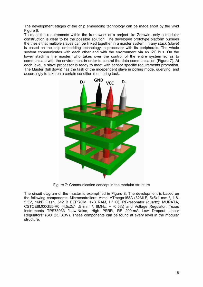
The development stages of the chip embedding technology can be made short by the vivid Figure 6. To meet the requirements within the framework of a project like Zerowin, only a modular construction is clear to be the possible solution. The developed prototype platform pursues the thesis that multiple slaves can be linked together in a master system. In any stack (slave) is based on the chip embedding technology, a processor with its peripherals. The whole system communicates with each other and with the environment via an I2C bus. On the lower stack is the master, who takes over the control of the entire system so as to communicate with the environment in order to control the data communication (Figure 7). At each level, a slave processor is ready to meet with sensor specific requirements promotion. The Master (full down) has the task of the independent slave in polling mode, querying, and accordingly to take on a certain condition monitoring task.
Figure 7: Communication concept in the modular structure
The circuit diagram of the master is exemplified in Figure 8. The development is based on the following components: Microcontrollers: Atmel ATmega168A (32MLF, 5x5x1 mm ³, 1.8-5.5V, 16kB Flash, 512 B EEPROM, 1kB RAM, I ² C), RF-resonator (quartz): MURATA, CSTCE8M00G55-R0 (4.5x2x1 .5 mm ³, 8MHz, + -0.5%) and Voltage Regulator: Texas Instruments TPS73033 "Low-Noise, High PSRR, RF 200-mA Low Dropout Linear Regulators" (SOT23, 3.3V). These components can be found at every level in the modular structure.
GND VCC D+ D-
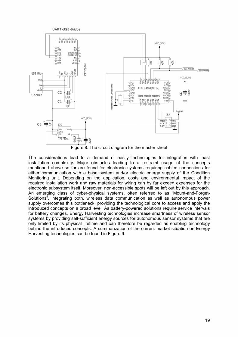
19
Figure 8: The circuit diagram for the master sheet
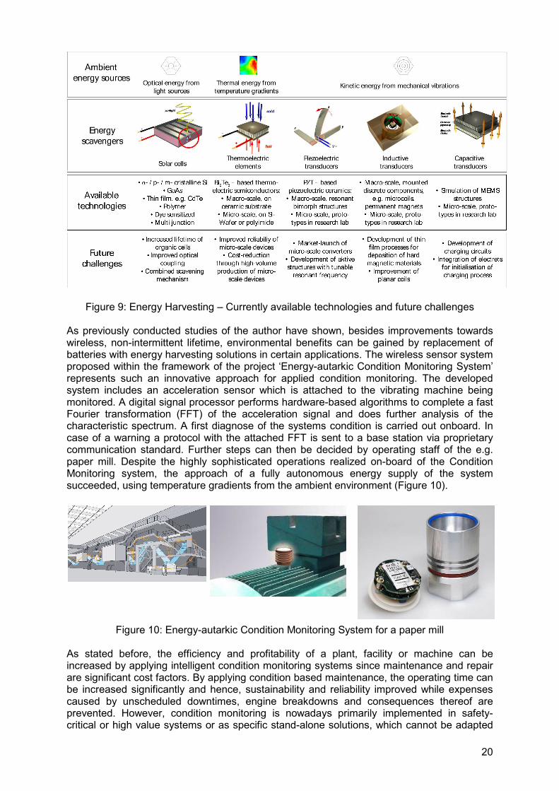
The considerations lead to a demand of easily technologies for integration with least installation complexity. Major obstacles leading to a restraint usage of the concepts mentioned above so far are found for electronic systems requiring cabled connections for either communication with a base system and/or electric energy supply of the Condition Monitoring unit. Depending on the application, costs and environmental impact of the required installation work and raw materials for wiring can by far exceed expenses for the electronic subsystem itself. Moreover, non-accessible spots will be left out by this approach. An emerging class of cyber-physical systems, often referred to as “Mount-and-Forget-Solutions”, integrating both, wireless data communication as well as autonomous power supply overcomes this bottleneck, providing the technological core to access and apply the introduced concepts on a broad level. As battery-powered solutions require service intervals for battery changes, Energy Harvesting technologies increase smartness of wireless sensor systems by providing self-sufficient energy sources for autonomous sensor systems that are only limited by its physical lifetime and can therefore be regarded as enabling technology behind the introduced concepts. A summarization of the current market situation on Energy Harvesting technologies can be found in Figure 9.
20
Figure 9: Energy Harvesting – Currently available technologies and future challenges
As previously conducted studies of the author have shown, besides improvements towards wireless, non-intermittent lifetime, environmental benefits can be gained by replacement of batteries with energy harvesting solutions in certain applications. The wireless sensor system proposed within the framework of the project ‘Energy-autarkic Condition Monitoring System’ represents such an innovative approach for applied condition monitoring. The developed system includes an acceleration sensor which is attached to the vibrating machine being monitored. A digital signal processor performs hardware-based algorithms to complete a fast Fourier transformation (FFT) of the acceleration signal and does further analysis of the characteristic spectrum. A first diagnose of the systems condition is carried out onboard. In case of a warning a protocol with the attached FFT is sent to a base station via proprietary communication standard. Further steps can then be decided by operating staff of the e.g. paper mill. Despite the highly sophisticated operations realized on-board of the Condition Monitoring system, the approach of a fully autonomous energy supply of the system succeeded, using temperature gradients from the ambient environment (Figure 10).
Figure 10: Energy-autarkic Condition Monitoring System for a paper mill As stated before, the efficiency and profitability of a plant, facility or machine can be increased by applying intelligent condition monitoring systems since maintenance and repair are significant cost factors. By applying condition based maintenance, the operating time can be increased significantly and hence, sustainability and reliability improved while expenses caused by unscheduled downtimes, engine breakdowns and consequences thereof are prevented. However, condition monitoring is nowadays primarily implemented in safety-critical or high value systems or as specific stand-alone solutions, which cannot be adapted

21
one-to-one to other applications. The cost awareness with 5000 Euro per hour if the mill has an unexpected shot down is compared with the automobile industry low. This is on the other hand the advantage of the autonomous microsystem using harvesting energy because the hardware (LCU and Cu-cable) as well as the set up and implementation have a much more significant influence. In the future there will be a significant market with sophisticated while adapted solutions. The development of micro systems and packaging technologies in recent years enables the development and implementation of more complex and reliable sensor devices for condition monitoring. Due to reduced size and improved mechanical robustness the possibilities and the field of application have enlarged. Since condition monitoring is nowadays usually not included in designs of electronic products and systems, the possibility of retrofitting must be given. Therefore, the monitoring system should be small and easy to be integrated into any product. However, for detecting precursor parameters, system parameters or environmental loads for life time estimation an appropriate sensor device and measurement equipment is required. To mount the sensor devices to the monitored system, proper places providing significant data have to be figured out. In order to be applicable to various types of products and thus a broad range of application, monitoring devices must be sufficiently robust to withstand all conceivable environmental impacts. Condition monitoring of electronic systems is more difficult than monitoring most mechanical systems due to more complex structures and nano- or micro-scale effects. A monitoring system should not cause unwanted interference with the monitored system. Especially in electronic systems, the integration of monitoring circuits needs to match various requirements, such as EMC, for instance. A further requirement is that the lifespan and the reliability of the monitoring device must necessarily exceed that of the monitored product. Any unexpected failure of systems results in decrease of profits. Especially if complex and expensive manufacturing facilities are stopped or expensive products (e.g. single-units) are faulty, costs can be very high. Loss of comfort, such as cancelled flights and delayed trains can lead to bad reputation, causing falling profits as well. In some cases, e.g. difficult to access machines such as offshore wind turbines, resolving an unexpected failure can take a long time (in that case depending on the weather). During that time no electric energy is produced and thus high financial losses may occur. In many cases the damage caused by a failure can be minimized if machines are turned off instantly as soon as a problem is detected. This is the case if, for instance, expensive tools, installed in fast running machines are damaged due to a delayed machine-stop in case of error. Through condition monitoring problems can be detected very fast and appropriate actions can be implemented quickly. Too early replacement of parts can be avoided because the system status is known and the remaining life time can be estimated. Exploiting the entire lifespan of parts increases the operating time and thereby saving money as well. Knowing the time of failure also reduces the amount of spare parts hold in stock because just in time ordering can be done. Another important issue is that the technology has to prove economically feasible. The costs of the monitoring system, including installation and operation, must not be higher than the costs the prevented failure would have caused. The Re-use of products is a key measure of an overall waste prevention strategy. Used products or their individual components are designated for use in new products. In order to apply appropriate handling at the end-of-(first) life, precise information on the product’s re-use potential is required. By using condition monitoring technologies, the potential for re-use can be determined. By reusing products less material and energy are needed compared to producing new ones. Therefore by using Condition Monitoring sustainability can be improved as well.
22
As stated in [4], the quality in reused products is not an issue at all. In fact, studies have shown that second life electronic equipment, if correctly remanufactured, can be more reliable than new. As described, failures in production lines are spotted quickly, therefore none or less faulty products, which in worst case have to be scrapped, are produced. Last but not least, failures in general can be a danger for health, safety, the environment and life. Thus any failure recognized by a monitoring system on time is a great benefit. In the following an adapted Condition Monitoring System for Photovoltaic Power Converter is exemplary shown. This is especially interesting, for it is an environmental friendly renewable energy producing technology. The major failure causes of photovoltaic converters are temperature shifts resulting in solder and bond-wire fatigues of the IGBT power modules (see Figure 11).
Figure 11: Open IGBT-Module
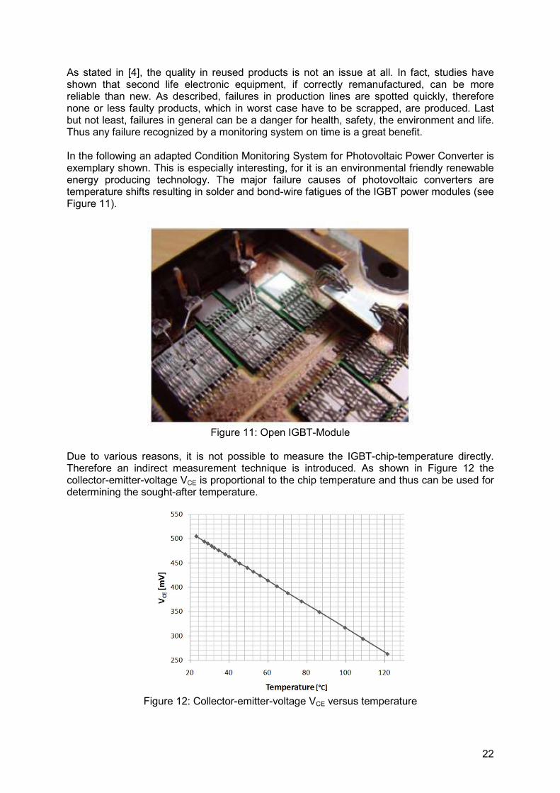
Due to various reasons, it is not possible to measure the IGBT-chip-temperature directly. Therefore an indirect measurement technique is introduced. As shown in Figure 12 the collector-emitter-voltage VCE is proportional to the chip temperature and thus can be used for determining the sought-after temperature.
Figure 12: Collector-emitter-voltage VCE versus temperature

23
In order to perform a life time prognostic, the measured temperature and temperature shifts are applied to the physics of failure model. This approach is called „Life Time Calculation“ and is realized in data loggers. Due to high currents (up to one hundred or more Amperes) and high voltages (couple of hundred Volts), the robustness of the condition monitoring system is crucial. Furthermore, the environmental temperature, the converter is exposed to, is an important factor. Temperatures can range in some environments, such as deserts, from below zero degrees Celsius in the nighttime to more than a hundred degrees Celsius during the day. This again shows the requirement of robustness of the monitoring system. The spare space in converter modules is rare and usually no room has been allocated for monitoring systems in the design-phase. Therefore the later-on installed monitoring system has to be small in size. The lifespan of photovoltaic panels is indicated with around 30 years. This implies that the condition monitoring has to work properly for even more than 30 years. Using condition monitoring systems has two positive economic and environmental consequences, respectively: First of all, the down-time of the system is minimized. In the case of photovoltaic-systems, longer run-time is equal to more electric power produced. In that case the energy is produced regenerative, therefore non-polluting. The more energy is being inducted into the grid, the higher the return on investment. A grid system based on renewable energy will only be successful if the reliability of the energy production is equal to or higher than conventional systems. To ensure the reliability of smart grids, made up of various (small) power producing systems, the reliability of each single unit has to be ensured. This requirement can be fulfilled by using condition monitoring. The other advantage is the utilization of a longer lifespan of the alternating-current converters. That means less energy and material are needed for new converters. By using condition monitoring systems, preventive exchange of the converters is no longer needed. They are replaced in case of an upcoming failure only, which reduces the maintenance and acquisition rate, hence the operational costs. The second approach is the Advanced Condition Monitoring Unit, which monitors the drift in parameters related to the system-to be-observed in order to allow diagnostics of the systems health. Again the example of IGBT-modules used in power converters in PV-plants is described. Two significant system-parameters are observed. On the one hand, the temperature within the module is obtained again by measuring the collector-emitter-voltage. This allows conclusions to the thermal resistance (see Figure 13) of the module. This is a suited indicator for the health of the solder-layers within the power module. The solder degradation is, as can be seen, leading to higher thermal resistance (difference of red and blue curve in Figure 13).

24
Figure 13: thermal behaviour within a new (blue curve) and aged (red curve) power module
The second relevant failure-mechanism is the wire bond lift off. Figure 14 shows that wire bond lift off is detectable as well as failure of single IGBT-chips by monitoring VCE. The red curve represent VCE while a current of 400 A is being applied to the module consisting of six IGBT-chips in parallel. The more wire bonds and especially the more chips are disconnected (numbers next to the red curve), the electrical resistance as well as the temperature increase and therefore VCE rises.
Figure 14: VCE versus number of disconnected wire bonds and chips at load current
3.3 PC Condition Monitoring
The following sections introduce the concept of PC condition monitoring. The concept relies on the monitoring the life cycle loads experienced by primary system PC components in order to facilitate usage qualification and therefore more efficient and cost effective triage operations at EOL. A report published in 2009 by the Green Electronics Council (GEC) concerning electronics design to enhance reuse/recycling value has termed “triage” as the
25
“inventorying, sorting and as appropriate, the testing, of incoming material in order to route into the selected business activities” (GEC 2009). This contrasts with previous approaches to condition monitoring of computer equipment in that embedded hardware and software technologies already present in PC systems are used for purpose of monitoring the lifecycle loads as opposed to the introduction of new sensor hardware. A method of data retrieval is developed in the following sections using RFID at a proof of concept level that demonstrates applicability of the concept in refurbishment operations. The concept is applicable for CS1 and CS3 as it allows quality determination of used primary system computer components.
3.3.1 Methodology
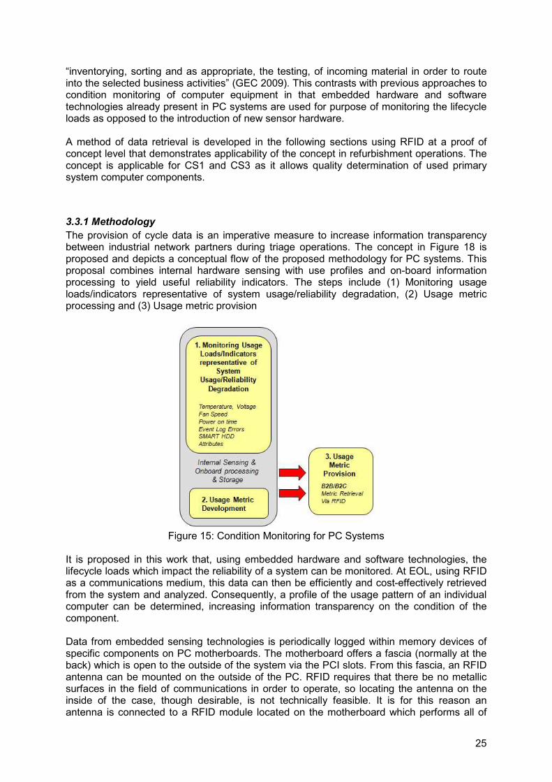
The provision of cycle data is an imperative measure to increase information transparency between industrial network partners during triage operations. The concept in Figure 18 is proposed and depicts a conceptual flow of the proposed methodology for PC systems. This proposal combines internal hardware sensing with use profiles and on-board information processing to yield useful reliability indicators. The steps include (1) Monitoring usage loads/indicators representative of system usage/reliability degradation, (2) Usage metric processing and (3) Usage metric provision
Figure 15: Condition Monitoring for PC Systems
It is proposed in this work that, using embedded hardware and software technologies, the lifecycle loads which impact the reliability of a system can be monitored. At EOL, using RFID as a communications medium, this data can then be efficiently and cost-effectively retrieved from the system and analyzed. Consequently, a profile of the usage pattern of an individual computer can be determined, increasing information transparency on the condition of the component. Data from embedded sensing technologies is periodically logged within memory devices of specific components on PC motherboards. The motherboard offers a fascia (normally at the back) which is open to the outside of the system via the PCI slots. From this fascia, an RFID antenna can be mounted on the outside of the PC. RFID requires that there be no metallic surfaces in the field of communications in order to operate, so locating the antenna on the inside of the case, though desirable, is not technically feasible. It is for this reason an antenna is connected to a RFID module located on the motherboard which performs all of

26
the necessary data modulation in order to initialize communications and to transmit information from the memory device to a reader. This component must be capable of processing the communications, and of additionally transmitting the volume of data which would be stored in a PC throughout a lifetime of use. This is outside the scope of existing RFID protocols which has led to its development in this deliverable. From the reader, data is transmitted to “middleware”, software which processes the information retrieved and analyses it to determine the patterns present and their impact on the reliability of a PC. This information can then be cross-referenced with current market values, based on trends in technology and the expected continued life of the used PC to give a value for the used system/component which accurately reflects its reliability, its functionality and the competing value offered by newer systems. In order to demonstrate the potential for the development of this type of technology, a proof of concept has been developed, which is the communications of large volumes of stored information from a RFID tag to a reader, and the streaming of this information to a computer for analysis. A volume of information can be transmitted in this way which would not be possible using currently available RFID technology. The next sections discuss the embedded hardware and software technologies in modern desktop systems that can enable usage qualification of systems.
3.3.2 Technology
In recent years, primary computer components have been designed with built-in sensors that monitor these components as to how they are being used. Temperature sensors are currently incorporated in all modern processors and certain high performance graphics cards. The rate of hardware faults occurring in the useful life of electronic components is tightly coupled with increasing temperature (Lall et al 1997). Voltages of primary system components are also software visible. Over-volting of CPUs is common among power users as a means of enhancing stability while over-clocking (over-clocking is the term used for changing a system’s configuration to that it runs at a faster speed than that recommended by the manufacturer). By recording the voltage supplied to key components, it is possible to detect voltage spikes or deviations which would indicate degradation of components. For example, the deviation of system voltages from nominal is an important indicator of the health status of the power supply. Certain PC fans are equipped with fan management ICs which monitor fan speed. The most basic fan failure detection is implemented using discrete components. Some available fan management ICs can monitor the fan’s commutation pulses and assert an alarm signal when no pulses are detected (Paparrizos 2005). Conventional hard disk drives (HDDs) based on rotating platter technology currently incorporate self-monitoring and reporting technology (SMART) diagnostics that permit the end user to evaluate the probability of drive failure at any given instant. Predictable failures are characterized by degradation of a certain attribute over time before the disk drive fails. Mechanical failures and other certain electronic failures are considered predictable because they show a degree of degradation before failing (Vichare and Pecht 2006). Examples of attributes set by drive manufacturers include read error rate, throughput performance, power-on hours, un-correctable sector count as well as a host of others (Seagate 1999). A survey carried out on a large population of disk drives in 2007 has established that scan errors, reallocation counts, offline reallocation counts, and Probational counts have the most significant impact on disk drive reliability (Pinheiro et al, 2007). Solid State drives (SSDs) have no moving parts therefore many of the parameters monitored by existing SMART technology are not applicable. Indeed, it is speculated that write/erase cycles are the only real failure mechanism present in solid-state storage (37). While these

27
disks have an infinite number of read cycles, they have a finite number of write cycles. New SMART technology developed enables user s to see the aggregated number of write cycles experienced by the disk over its lifetime (Silicon Systems 2005). Moreover certain hard disks employ accelerometers which increments a counter should the drive experience a shock over a defined threshold. The diagnostic technologies mentioned above have been incorporated primarily as health monitors to provide feedback to users on the current operating health of their systems. This feedback is particularly of interest to power users where “over clocking” is common practice causing their system components to run at higher temperatures than intended by the manufacturer. 3.3.3 Prototype Development In terms of the frequency and types of RFID technology that would be most suitable for the proposed system, the read range, data rate, ease of development and tolerance of barriers were all taken into consideration. Low frequency technologies were considered to be too limited with regard to data rate, while the complexity of the antenna design required for the functioning of the far-field magnetic coupling made the ultra high frequency (UHF) and microwave frequency ranges unsuitable as a prototype. Following adoption of the technology, it is likely that the advantages offered by far-field coupling would mean the eventual adoption of UHF technologies, however technological limitations in the process of creating and testing a prototype device precluded their immediate use. High Frequency (HF) technology, operating in the 13.56 megahertz (MHz) frequency range, is demonstrable in a lab environment, using oscilloscopes. Furthermore, microcontrollers operating at frequencies of up to 16MHz are relatively common and inexpensive. The design of RFID circuits is relatively common at this frequency, meaning there is readily available literature about the process of coupling and circuit design. Data Reduction Life cycle loads associated with hardware reliability degradation for example temperature, and voltage may be graphically presented by a series of peaks and valleys in a specific time domain. However to store this information over the entire lifecycle of a PC taking into account the maximum permissible sampling rate capable by the sensing devices (approx 1 second) would mean larger memory requirements introducing increased cost. Furthermore limitations imposed by the data rates of RFID also limit the volume of data being transmitted at EOL. A means of data reduction or screening is therefore required to condense these load histories. Data simplification methodologies condense load histories without sacrificing important damage characteristics. Existing methods for data simplification include data reduction and cycle counting (Ramakrishnan and Pecht 2003). While data reduction allows the user to specify a screening level where a specific range of certain data can be eliminated, cycle counting methods are used to transform a time history consisting of several peaks and valleys into an equivalent cyclic history (Ramakrishnan and Pecht 2003). Cycle counting methods are usually employed in systems which monitor fatigue and stress in materials. To analyse and monitor these device stresses, cycles which place less stress on the device and cause less damage can be removed from the load analysis. A cycle occurs when the applied load returns the material to the state it was in before the load occurred. When the load reaches a value at which the stress was previously changing in the reverse direction a full cycle occurs. The stress path beyond this point is the same as if the initial loading had not occurred and it no longer affects the behaviour of subsequent cycles (Mishra et al 2004). For temperature analysis one cycle is identified as a temperature increase and

28
the corresponding decrease. Amongst the most common methods of reducing data to cycles are: • Level counting • Peak counting • Simple range/mean counting • Rainflow Counting • Probability density function (PDF) Of these the rainflow counting method and its variations are the most widely accepted cycle counting techniques as it can handle non-repeating time histories and results in the least amount of data loss. Using data reduced by cycle counting, damage calculation times can also be greatly reduced. An investigation into the efficacy of rainflow cycle counting has been carried out for this application. By monitoring the temperature of a PC using C in conjunction with windows management instrumentation (WMI), a log of time series temperature was obtained, and cycle counting was carried out on the sample. The main purpose of this cycle counting technique is to ensure that the more relevant data is highlighted among the rest of the data. The mean temperature at which cycles occur needs to be recorded, as unlike stress measurements the temperature is not likely to fluctuate about zero and is likely to cycle about a varying mean temperature. This method of counting also allows for the use of a cut-off where only temperature cycles above a certain level are recorded. Before cycle counting the temperature data must be filtered to turning point data only, this means that all time history would be lost if time indexing of the inputs did not take place. There are several filtering techniques used to reduce data, the method used in this application is known as Ordered Overall Range filtering. This algorithm must be developed to suit the temperature data being analysed. The graphs in Figure 19 and Figure 20 show the results of the cycle counting analysis. Figure 18 compares the number of cycles at each mean temperature with each period, while Figure 19 shows the same results compared under the headings of mean temperature and temperature swing amplitude. In order to capture all of this data, it is necessary to express the results as a four dimensional array. A limit of 145 kilobytes was put on the data to be stored, owing to the limitations of the SD card being used, and as this would represent a transfer time of approximately one second using HF RFID.

29
Figure 16: Results of period and mean temperature analysis
Figure 17: Results of temperature swing versus mean temperature analysis Temperature data was broken down, as shown in Figure 21, into 25 blocks, each representing a specific temperature swing, with a resolution of one degree Celsius.

30
Figure 18: Block diagram of data storage methodology Within each of these blocks is 11 further blocks, each representing a different mean temperature, with a temperature resolution of three degrees centigrade. Finally, within each mean block are 170 frequency bins, of 6 bytes each, each representing a specific period of temperature swing, with a resolution of 30 seconds. The number in a bin is incremented every time temperatures cycle of that frequency, mean and amplitude occurs. In the worst case scenario, where the same temperature swing about the same mean is exhibited throughout the lifetime of the system, that specific bin would take almost 8years to fill. This represents a very unlikely confluence of conditions, and would be very improbable in practice. Nonetheless, for comparison purposes, if temperature values were to be constantly stored using the same sample rate over the same period, over 8.3 MB of storage space would be required, at one byte per sample as shown in Figure 22.
Figure 19: Log file size with data reduction verses no data reduction
Therefore, through the implementation of this data reduction method, the volume of data is reduced to less than two percent of its potential maximum size. To transfer this data using RFID at 848kilobits per second would take in excess of one minute. Swift transfers of data

31
are required, as interference is common in industrial environments, and through the reduction of the length of time taken to transfer data, the probability of an error is reduced. One restriction of rainflow counting using the ordered overall range method is that the algorithm must be applied to a block of data, and cannot be implemented on real-time, running data. This places some restrictions on the maximum temperature swing that could be recorded, as device memory constraints dictate how large the maximum data blocks can be, and thus how large the maximum possible recording period is. RFID Communication The previous section has investigated methods of data reduction for life cycle data based on the rainflow counting methodology. This section focuses on RFID communication aspects. Following the choice of HF technologies, it was necessary to decide upon a protocol on which to base the operation of a prototype device. Although the protocols currently in use do not allow for the transmission of the volume of data required, by basing the fundamental operation of the prototype on an existing protocol a large amount of complexity surrounding initiating communication between the reader and the tag could be bypassed. Basing the prototype on existing protocols also allowed for the use of existing RFID reader technology without the need for excessive modification of the fundamental operating principles. The MIFARE protocol was selected the most appropriate protocol for designing a prototype tag. A user programmable “ELEKTOR“ RFID reader shown in Figure 23, allowed the modification of the firmware on the reader without affecting the low-level functionality.
Figure 20: ELEKTOR RFID reader The MIFARE protocol features methods for the identification of a single tag type, multiple tag handling, and error handling by means of both the use of byte level parity bits and frame level cyclic redundancy checks. The error checking functionality is necessary in order to deal with the amount of data which would be transmitted using the prototype tag, as an increased volume of data increases the probability that an error will occur at some point during transmission. Tags normally associated with this standard are used as identification cards for such purposes as building access control. These are passive tags, and are used only within a short range of the reader. The objective in development was to retain all of the functionality associated with the protocol, allowing it to continue to recognise the common RFID tags and perform access control functions, while at the same time allowing the reader to communicate with and identify the newly designed tag, and to modify the way in which data is handled so that the increased volume of information could be processed using the existing hardware.
32
Developing RFID communication required utilising the ISO/IEC 14443 standard for contactless integrated circuit cards (The ISO/IEC 14443 standard, defines the physical characteristics, the radio frequency power and signal interface, initialisation and anti-collision processes and the transmission protocol and governs the communication between devices), and the modification of a MIFARE reader to allow the transmission of greater volumes of data than would normally be permitted. In order to implement these requirements, it was necessary to first design a circuit which would behave exactly in the same manner as a proximity integrated circuit card (PICC) from the perspective of the reader/proximity control device (PCD), but also be capable of transmitting a much greater volume of data. A circuit diagram of the RFID hardware is shown in Figure 24. The module contains a ATmega16 microcontroller with integrated EEPROM in conjunction with an RFID antennae. The role of the microcontroller is data flow control with temperature sensing devices on the CPU and other hardware sensing devices on the super I/O chip on the motherboard. In addition it plays a role in data reduction of the acquired lifecycle data as demonstrated in the previous section. The EEPROM stores the lifecycle information until EOL where this information is transmitted to middleware for analysis via the RFID circuit shown.
Figure 21: RFID Circuit
Figure 24 illustrates a tuned receiver (13.56MHz), leading to a rectifying diode and voltage divider. The output is fed into a comparator which provides a digital signal for the microcontroller (not shown). The following sections step through (A) Modulation, (B) Physical Communications Interface, (C) State Machine Implementation, and (D) Simulation aspects (A) Modulation The ISO/IEC 14443 standard specifies a different type of modulation and encoding to be used in communications in each direction between the PICC and PCD. As the technology is based around the assumption that power for the tag will be provided by the reader, the purpose of the modulation is to ensure that the reader is transmitting for a maximum possible proportion of the time during communication. This allows the PICC to gather enough of the power through inductive coupling to be capable of responding.
33
PCD to PICC In communications from reader to tag, the modulation in use is 100% amplitude modulation. However, it is necessary for the PCD to provide enough energy to allow the PICC to respond, so the communication is encoded so that information may be transmitted with minimal disruption to the carrier wave. In this manner, the energy required to enable PICC circuitry operation may be transmitted entirely from the PCD, and the pauses in the carrier signal, which are required to communicate data, are sufficiently short to ensure that a PICC remains energised throughout the communications.
Figure 22: ISO 14443 definition for "pause" in communication
The bit representation sequences as defined in the ISO 14443 standard are described in Table 1, and the standard definition for the “pause” transmitted is shown in Figure 24 .
• Sequence X
• After a time of 64/fc a “pause” shall occur
• Sequence Y
• For the full bit duration (128/fc) no modulation shall occur
• Sequence Z
• At the beginning of the bit duration a “pause” shall occur
Table 1: Signal sequences for PCD to PICC communication defined in ISO 14443 standard In order to differentiate between the transmission of signals, the provision of energy for response from the PICC and the absence of a PCD entirely, the sequences from Table 1 are used as described in Table 2. Specific combinations of sequences are also used to identify the start and ends of communications. In this way it is ensured that the absence of data can easily be distinguished from the transmission of a continuous sequence of ‘0’s.
• Logic “1” • Sequence X
• Logic “0” • Sequence Y with the following two exceptions
• If there are two or more contiguous “0”s, sequence Z shall be used from the second “0” on

34
• If the first bit after a start of frame is “0”, sequence Z shall be used to represent this and any “0”s which follow directly thereafter
• Start of communication
• Sequence Z
• End of communication
• Logic “0” followed by sequence Y
• No information • At least two sequences Y
Table 2: Information coding for PCD to PICC communications
PICC to PCD Communications between the PICC and the PCD are performed by means of increasing or decreasing the load applied to the RF field generated by the PCD. This in turn affects the magnetic field intensity, which is detected at the PCD, and decoded to recover the transmitted information.
• Sequence D
• the carrier shall be modulated with the subcarrier for the first half (50%) of the bit duration
• Sequence E
• the carrier shall be modulated with the subcarrier for the second half (50%) of the bit duration
• Sequence F
• the carrier is not modulated with the subcarrier for one bit duration
Table 3: Signal sequences for PICC to PCD communication defined in ISO 14443 standard These communications are also encoded using a form of Manchester encoding, whereby modulation is applied during the first half of a bit period if the bit represented is a ‘1’, or in the second half if the bit is a ‘0’, as shown in Table 3. Communication is always preceded by a ‘1’, and the modulated portion of each communicated bit starts with the load applied. Table 4 shows how information is communicated using the sequences defined in Table 3.
• Logic “1” • Sequence D
• Logic “0” • Sequence E
• Start of communication
• Sequence D
• End of communication
• Sequence F
• No information • No subcarrier
Table 4: Information coding for PICC to PCD communications Error Checking The ISO 14443 standard defines error checking protocols which ensure the validity of information communicated in both directions. Odd parity bits are appended to all communications of greater than eight bits length, and for standard communications two cyclic redundancy check (CRC) bytes are appended to each frame. The polynomial for the calculation of the CRC bytes is x16 + x12 + x5 + 1, and the initial value is defined as 6363 hexadecimal. (B) Physical Communications Interface At the physical level, it is not necessary to be concerned about the function of the data which is being transmitted, and only the methods of communication need to be considered. For the
35
purpose of the RFID tag and reader, the physical layer is implemented in the hardware which performs the modulation and demodulation of the transmitted signals, and by the software on the PICC which encodes and generates the outgoing signals, and decodes those incoming signals into simple digital data, which may then be passed to the higher levels of the code, where the resultant data is analysed and appropriate responses generated. This section examines the process for the development of software which implements the requirements of the physical interface. Owing to the requirements of the standard governing RFID communications, as explained in section 0, it was necessary for the hardware code which affected the physical transmission of data to be written in assembly language. This was preferable to writing it in the more powerful language of C because while C may simplify the programming process, the compiler performs optimisation of any C code entered, which makes it impossible to predict exactly the timing of the final implementation which is programmed to the microcontroller. Given a clock at the carrier frequency, 13.56MHz, transmissions from the PICC during the application of modulation change every eight system clock periods, which is a narrow time frame in which to execute the intervening commands. The advantage of programming in assembly language is that each command in assembly has a specific execution time, defined in numbers of clock periods, which is defined in the datasheet of the device in question. This allows the code writer to determine, by counting commands and considering the clock frequency, exactly the length of time which will pass between the alteration of the voltages on the output pins, guaranteeing that the signals from the device will conform as closely as possible to those laid out in the communications protocol. Software Solution Initially, the possibility of performing encoding, decoding and error checking using assembly code was considered. This solution was originally dismissed as requiring too much assembly coding. An initial software solution was developed in which the transmission of data was performed with assembly language. After examining the cost in processing time and memory of using C code to perform these functions, it was decided to revisit the possibility of performing basic error checking, encoding and decoding using assembly code functions. There were several advantages to the ability to encode the data as it was transmitted and to decode data as it was received over the previous solution - which stored samples sequentially, and subsequently analysed the resultant data to recover the information which was transmitted. Primarily, the amount of time required to analyse data is reduced drastically, as incoming data is analysed in real time, as the bits arrive at the input pin. This allows the program to operate within the requirements laid out in the standard outlined. As a result a further examination was made into the viability of using assembly language to perform the encoding and decoding of data as it was received. Encoding Encoding of data in the program was performed by the asm_TX function. The purpose of the encoding section of the assembly code was to transmit information in the manner required by the protocol, so that it could be received and decoded by a MIFARE RFID reader. The code for transmission of data operates by taking information which is stored in the IObuffer array. In IObuffer, the total number of bits to be transmitted is stored in the first address in the array, and all sequential bytes contain the information to be transmitted. A major problem with encoding information using assembly was the restriction on timing. Owing to the fact that the modulation frequency for transmitting responses to the reader was one sixteenth of the carrier frequency, it is necessary to load the input waveform once every eight system clocks. Given the fact that the assembly command to alter the signal on an output pin required 2 system clocks to operate, this only allowed six system clocks of free processing time between each event during the modulated half of each transmitted bit. As

36
such, all calculations relating to subsequent bit transmissions were performed during the unmodulated half of each bit, which allowed 64 clocks in which to perform the necessary operations. During the development of the code for transmission of information further issues arose. Any viable code for this purpose would have to follow several ‘branches’ depending on what was required. These include two normal branches, appending a zero or a one, and several more complicated branches, such as appending a parity bit, or accessing the next byte for transmission. While none of these processes were necessarily impossible, it was vital that each branch within the code would take exactly the same length of time, which made the process very exacting, as changing any branch would have a knock-on effect on any successive code, and it was necessary to ensure the cumulative time taken between the output events was consistent.
Figure 23: Possible bit sequences at output of microcontroller
It is possible to describe the three main operations to be performed each time the PICC would transmit a bit in normal operation. These are best described by observing Figure 25. If the next bit to be transmitted was the same as the current bit, as shown in 25(a) and (d), then one modulated half bit must occur before the subsequent unmodulated half-bit. If the sequence is “01”, then two modulated half bits occur with no unmodulated time in between. Finally, if the sequence is “10”, nothing needs to be done before the next bit, as there are two consecutive unmodulated half bits, as shown in 25(c). As the output is required to change once every eight clock periods during the modulated half-bit, all of the computations were carried out during the unmodulated half, which is 64 clock periods in duration. While the signal is being modulated, a counter monitors the number of modulations which have occurred. This counter is loaded with the required number of modulations by considering the current bit and the next bit as described above. Each of these processes was relatively quick. Adding a zero was found to take only six clock periods, while adding a one took eight. By putting these processes towards the end of the unmodulated half bit, it was possible to add the remaining required processes before them, and to ensure that each process is started at the same time regardless of which branch it is being accessed from. Figure 26 is a detailed examination of the operation of the section of code governing transmission of data. As described previously each communication from the PICC is required to start with a ‘1’, so the initial transmission of data is four sequences of modulation. Following this, there are three paths, depending on which of the following actions is being performed:
a) Transmitting normally b) Transmission has reached the end of a byte and needs to append
parity c) Transmission has appended the parity bit and needs to fetch the next
byte from the IObuffer
The decision is made by observing the “bits remaining in byte” counter, and if it is 0, then a parity bit must be added. If the counter is less than 0, an additional byte should be fetched from memory, and the counter should be reset to eight bits.
00 10 1 101
(a) (b) (c) (d)

37
Concurrently, each time a bit which is not a parity bit is transmitted, the “overall bits” counter is decremented. This is initially loaded from the first address in IObuffer, and when it reaches 0, all of the required information has been transmitted by the PICC. At this point, if the final bit was a ‘1’, the function can exit immediately, as the modulated half bit has already been transmitted, while if it is a ‘0’, a final modulated half-bit needs to be transmitted before exiting.
Figure 24: Flow diagram outlining operation of transmission section of assembly code
Decoding As with the encoding section of the solution, the decoding function, asm_RX, performed the function of receiving the information being transmitted by the PCD, decoding the signals and storing the information received in the IObuffer. Because the number of samples in a bit is known, it was possible to write code which, at the end of eight samples, would decode which bit has been received. This is done by counting logic high signals. When a transition from low to high is registered, the count is reset. As long as the input remains high, the count is incremented. The hardware involved is described in later sections, and performs the function of converting the carrier frequency, when transmitted, to a ‘high’ logic level, and the pauses to a ‘low’ logic level.
Mod
count=0?
Set mod. count=4
Load output
Wait
Unload output
Dec. mod. count
Dec bits in byte
Bits
remaining
in byte?
Next bit?
Current
bit?
Current
bit?
Update parity
Set mod. count=4Set mod. count=8
Bits
remaining
overall?
Parity bit Reset parity
Set mod. count=4
Load output
Wait
Unload output
Dec. mod. count
Current
bit?
Mod
count=0?
Dec. bits overallLoad next byte
Reset parity
Exit
1 0
Yes
No
10
1
0
1
0
<00
>0
0
>0
1
0
Yes
No

38
By examining the definition of a “pause” as shown in 27, it can be seen the delay between the initial deviation from 100% of the carrier amplitude to 60% of the amplitude after the “pause”, a minimum of 2 µs, and a maximum of 3.4 µs passes. Allowing for the best and worst cases and taking into account a sampling period of 1.18 µs, a minimum of one and a maximum of three low samples may be recorded during the pause. From Table 1, a pause will begin either at the start of a bit period or half way through the bit. Allowing for the best and worst cases above:
a) If three or less consecutive high samples are recorded before the end of a bit, the sequence transmitted corresponds to a sequence X, meaning a logic ‘1’ was transmitted
b) If between nine and eleven consecutive high samples occur before the end of a bit, the sequence was the last one to three samples in the preceding sequence X, and the eight high samples of a sequence Y, representing a logic ‘0’
c) If between five and seven consecutive high samples are recorded before the end of a bit, sequence Z was transmitted, meaning either the start of communication or second or subsequent contiguous logic ‘0’
d) If greater than 12 high signals are received, the signal is either a sequence Z followed by a sequence Y or two consecutive sequences Y, in either case denoting the end of the data communicated.
In the implementation of these rules in the code if one, two or three samples are found to have been high at the end of a bit, then that bit is stored as a ‘1’. If greater than four samples were high, it is recorded as a ‘0’, unless greater than 12 sequential samples were high, as this is the indication of the end of transmission. While the function sequentially receives and decodes bits, it rotates them into a temporary memory address, temp, and calculates the parity for the current byte. On receiving the ninth bit since the start of a byte it tests the parity bit to ensure that it is correct, and stores the contents of temp in the IObuffer at the next location. If the parity bit is not correct for any received byte, the function terminates.

39
Figure 25: Flow chart for receiving and decoding of data
At the end of transmission, the last two bits received are discounted as they are the two end bits, and the total number of bits received is stored in the first address in IObuffer. At this point the amount of information referred to by the first address in IObuffer should be stored in the following addresses. (C) State Machine Implementation The ISO 14443 standard describes the higher operations of the PICC and reader in the form of a state machine. This model significantly simplifies the protocol from a design perspective, as the PICC may be programmed to remain in any individual state until such time as it receives specific commands. Once these commands are decoded, the PICC can move onto the next state in the sequence, depending on the exact command received. It was decided to use the state machine as the model for the functionality of the main part of the PICC program. In this way, as the PICC receives commands from the PCD it is only necessary to compare them to a predefined selection of commands. For each state, only certain specific commands will allow progression to the sequentially following state, while a different selection of commands will cause the PICC to either reset or to go into a ‘Halt’ state. A synopsis of those commands which were defined in the program is presented in Table 5. Any command not catered for in a particular state will be ignored by the PICC.
• Abbreviation • Command • bits • Value
• REQA • Request Command, Type A
• 7 • 26h
• WAKE-UP/WUP
• Wake Up • 7 • 52h
• ATQA • Answer to Request, • 16 • Proprietary
Sample
pin
Clear 1s count
Dec .sample count
8
samples?
Previous
sample?
Increment 0s count Increment 1s count
>4 seq.
0s?Clear 0s count
Reset sample count
Dec.no. bits rcvd
9 bits
received?
<4 seq.
1s?
Rotate 0 into byteRotate 1 into byte
Update parity bit>12 seq.
1s?
Reset bits rcvd count
>12 seq.
1s?
Parity ok?
Store byte
Inc. data stored
Store outstanding
data
Update data stored
Exit
Exit:
Parity
Error
Exit::
Signal
Lost
1
0 1
0
Yes No
YesNo
YesNo
Yes
Yes No
No
No
Yes
YesNo
40
Type A
• SEL • Select Command • 8 • 93h: Select cascade level 1
• 95h: Select cascade level 2
• 97h: Select cascade level 3
• NVB • Number of valid bits • 8 •
• HALT • Halt • 32 • 50h+00h+CRC
Table 5: Synopsis of commands used in state machine For these more complex commands, governing data recovery and analysis, the higher programming language of C was used. This was possible as the ISO 14443 standard allows generous delays between transmission and receipt of blocks of data. Between the initial activation command for a device and its response, exactly 960 clock periods are required, or a total of 70.8µs. Between all other PCD transmissions and PICC responses, 960 clock periods is defined as the minimum response delay, while the delay is permitted to be anything up to almost half a second, or over 6.5 million clock periods. This allows ample time for complex operations to be performed in the code without concern for the exact timing of responses. Responses are only required to occur at a time equal to an integer multiple of bits periods since the last bit transmitted by the PCD. During inter-transmission delays it is possible to perform analysis on the data received and prepare the appropriate next data blocks for transmission without exact knowledge of the number of clock periods required. While it was not necessarily certain to what degree the optimisation performed by the compiler would affect the timing parameters between input or output events, once the program was implemented on hardware it was simple to add and modify delays to the code so that the requirements of the protocol were satisfied. The following is an overview of the states outlined in the ISO 14443 standard and the signals from the reader which would result in the progression to subsequent states. In order for communication of stored information to occur, the PICC must enter the active state. In order to simplify the debugging and testing process, three outputs of the microcontroller were configured to activate LEDs to indicate the state which the PICC was currently operating in. The LEDs were configured as follows: 001 Programmed, not yet in any state 010 Idle state 011 Ready state 100 Active state 101 Halt state State 1: Idle In this state the PICC is inactive until it encounters the field of a PCD, which gives it the power necessary to process commands. On detecting a PCD in range, the PICC enters receiving mode, and will remain there until such time as a transmission is received from the PCD or the PCD goes out of range. In order to exit the idle state, the PICC must receive either the seven bit request acknowledge (REQA), or wake up (WUP) command. On receiving any communications from a PCD, the PICC compares the information received with these values. If the value is as expected, the PICC automatically transmits the response, ATQA, and transitions to the next state. Should any other command be received, the comparison will return a ‘false’, and the PICC will return to receiving mode.
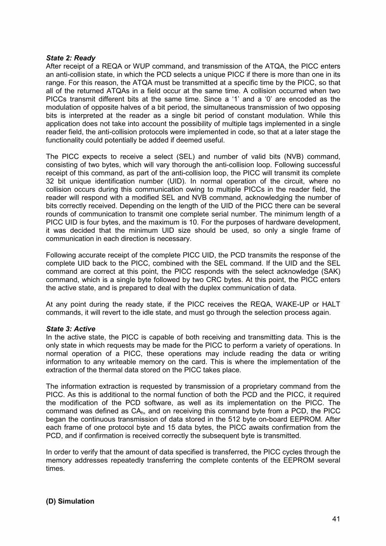
41
State 2: Ready After receipt of a REQA or WUP command, and transmission of the ATQA, the PICC enters an anti-collision state, in which the PCD selects a unique PICC if there is more than one in its range. For this reason, the ATQA must be transmitted at a specific time by the PICC, so that all of the returned ATQAs in a field occur at the same time. A collision occurred when two PICCs transmit different bits at the same time. Since a ‘1’ and a ‘0’ are encoded as the modulation of opposite halves of a bit period, the simultaneous transmission of two opposing bits is interpreted at the reader as a single bit period of constant modulation. While this application does not take into account the possibility of multiple tags implemented in a single reader field, the anti-collision protocols were implemented in code, so that at a later stage the functionality could potentially be added if deemed useful. The PICC expects to receive a select (SEL) and number of valid bits (NVB) command, consisting of two bytes, which will vary thorough the anti-collision loop. Following successful receipt of this command, as part of the anti-collision loop, the PICC will transmit its complete 32 bit unique identification number (UID). In normal operation of the circuit, where no collision occurs during this communication owing to multiple PICCs in the reader field, the reader will respond with a modified SEL and NVB command, acknowledging the number of bits correctly received. Depending on the length of the UID of the PICC there can be several rounds of communication to transmit one complete serial number. The minimum length of a PICC UID is four bytes, and the maximum is 10. For the purposes of hardware development, it was decided that the minimum UID size should be used, so only a single frame of communication in each direction is necessary. Following accurate receipt of the complete PICC UID, the PCD transmits the response of the complete UID back to the PICC, combined with the SEL command. If the UID and the SEL command are correct at this point, the PICC responds with the select acknowledge (SAK) command, which is a single byte followed by two CRC bytes. At this point, the PICC enters the active state, and is prepared to deal with the duplex communication of data. At any point during the ready state, if the PICC receives the REQA, WAKE-UP or HALT commands, it will revert to the idle state, and must go through the selection process again. State 3: Active In the active state, the PICC is capable of both receiving and transmitting data. This is the only state in which requests may be made for the PICC to perform a variety of operations. In normal operation of a PICC, these operations may include reading the data or writing information to any writeable memory on the card. This is where the implementation of the extraction of the thermal data stored on the PICC takes place. The information extraction is requested by transmission of a proprietary command from the PICC. As this is additional to the normal function of both the PCD and the PICC, it required the modification of the PCD software, as well as its implementation on the PICC. The command was defined as CAh, and on receiving this command byte from a PCD, the PICC began the continuous transmission of data stored in the 512 byte on-board EEPROM. After each frame of one protocol byte and 15 data bytes, the PICC awaits confirmation from the PCD, and if confirmation is received correctly the subsequent byte is transmitted. In order to verify that the amount of data specified is transferred, the PICC cycles through the memory addresses repeatedly transferring the complete contents of the EEPROM several times. (D) Simulation
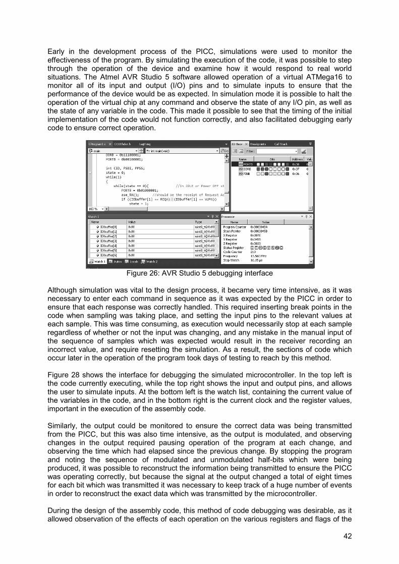
42
Early in the development process of the PICC, simulations were used to monitor the effectiveness of the program. By simulating the execution of the code, it was possible to step through the operation of the device and examine how it would respond to real world situations. The Atmel AVR Studio 5 software allowed operation of a virtual ATMega16 to monitor all of its input and output (I/O) pins and to simulate inputs to ensure that the performance of the device would be as expected. In simulation mode it is possible to halt the operation of the virtual chip at any command and observe the state of any I/O pin, as well as the state of any variable in the code. This made it possible to see that the timing of the initial implementation of the code would not function correctly, and also facilitated debugging early code to ensure correct operation.
Figure 26: AVR Studio 5 debugging interface
Although simulation was vital to the design process, it became very time intensive, as it was necessary to enter each command in sequence as it was expected by the PICC in order to ensure that each response was correctly handled. This required inserting break points in the code when sampling was taking place, and setting the input pins to the relevant values at each sample. This was time consuming, as execution would necessarily stop at each sample regardless of whether or not the input was changing, and any mistake in the manual input of the sequence of samples which was expected would result in the receiver recording an incorrect value, and require resetting the simulation. As a result, the sections of code which occur later in the operation of the program took days of testing to reach by this method. Figure 28 shows the interface for debugging the simulated microcontroller. In the top left is the code currently executing, while the top right shows the input and output pins, and allows the user to simulate inputs. At the bottom left is the watch list, containing the current value of the variables in the code, and in the bottom right is the current clock and the register values, important in the execution of the assembly code. Similarly, the output could be monitored to ensure the correct data was being transmitted from the PICC, but this was also time intensive, as the output is modulated, and observing changes in the output required pausing operation of the program at each change, and observing the time which had elapsed since the previous change. By stopping the program and noting the sequence of modulated and unmodulated half-bits which were being produced, it was possible to reconstruct the information being transmitted to ensure the PICC was operating correctly, but because the signal at the output changed a total of eight times for each bit which was transmitted it was necessary to keep track of a huge number of events in order to reconstruct the exact data which was transmitted by the microcontroller. During the design of the assembly code, this method of code debugging was desirable, as it allowed observation of the effects of each operation on the various registers and flags of the

43
ATMega16. After the assembly language had been completed, however, and it was ascertained that information could be transferred successfully, debugging the timing features of the program required automation in order to avoid highly repetitive analysis. In order to overcome this problem, it was necessary to set up stimuli in advance of running the simulation. This would automatically alter the inputs and outputs at the relevant times in order to facilitate much faster simulation of the program. Unfortunately, AVR Studio 5 does not support preloading of stimuli or logging of outputs. Further investigation revealed that AVR Studio 4, the previous version of the compiler program, did support stimuli and logging. Stimuli In the AVR Studio 4 software, inputs to any port can be preset to occur at specific times through the use of a stimulus file. Each file relates to only one eight bit port on a device, and a specific format of data is required in the file to ensure that it is interpreted correctly. Figure 29 shows the layout of a stimulus file. The first set of numbers is the clock number at which the input should change. The number after the colon is the hexadecimal representation of the eight pins of the port in question. These are numbered from seven down to zero. Since the only pin in use as an input is Pin 4 of Port B, the input alternates between ‘10’ when Pin 4 is set and ‘00’ when all pins are cleared.
Figure 27: Layout of stimulus file for AVR Studio 4
While this significantly improved the speed at which repetitive processes could be performed, it also required the timing for each command to be entered manually. This was quite time consuming, and changing the starting time of one command required recalculating the time for every subsequent change in the inputs. Added to this, as the inputs to be included represented the modulated data incoming from the PCD, rather than simple digital commands, it was necessary to calculate the pattern of modulated bits for each input to the PICC. Parity bits and CRC bits also had to be calculated and included. The process was therefore highly calculation-intensive, and as the timing for each value would determine every subsequent one, it was highly susceptible to human error. In light of this fact, a spread sheet was developed in Microsoft Excel which was capable of determining the sequence of stimuli for any given command. It was also capable of varying the length of a ‘pause’ to be any value in the permissible range defined in ISO 14443, and of starting the command at any given clock. The spread sheet functions by alternating the commands stored in vertical cells. As each ‘pause’ can reasonably be expected to be of more or less uniform length, every second timing line would simply be the previous time with the length of the pause added. The entire

44
sheet worked by starting from the least significant bit, calculating the pause to the next change in input, and then erasing the bit already handled. In this way, the same formula could be used in each calculating cell, and the sheet could be extended to calculate the timings for a command of any length. The first bit transmitted is a ‘Z’ signal for any command, so the first bit is always predefined. Subsequent timings were decided on the basis of the following formula, where A8 is the cell currently under examination, and B9 is the cell containing the start time of the previous pause: =IF(LEN(A8) = 1, "", IF(LEFT(A8, 3) = "101", B9 + 256, IF(LEFT(A8, 3) = "100", B9 + 192, IF(LEFT(A8, 2) = "01", B9 + 192, IF(LEN(A8) = 2, IF(A8 = "10", "", B9 + 128), B9 + 128))))) This operates on the basis of considering three possible conditions for the data, and depending on the length of data remaining to be processed.
Figure 28: PICC output sequences with delays highlighted for stimulus file generation
If the first two bits are ‘10’ then (if there are three or greater bits of data for processing) the first three bits are taken into account, as the ‘0’ will not require a change in the signal. As can be seen from Figure 30, if the third bit is a ‘1’, then the signal is ‘101’ (XYX), and the input should change 256 clocks after the start of the previous pause. If the third bit is a ‘0’, then the sequence is ‘100’ (XYZ). In this case the initial change for the ‘1’ took place half way through the bit interval, so the next change occurs 192 clocks later. If the first two bits are not ‘10’, then only the first two bits are taken into account, as the successive change in polarity occurs in the second bit. The possible conditions are ‘11’, ‘00’ or ’01’. In the case of ‘00’ (ZZ) and ‘11’ (XX), as the same bit is in use, the pause will start 128 clocks after the previous one. For the case ‘01’ (ZY), the pause starts 192 clocks after the previous one. The final condition is again when the first two bits are ‘10’ (XY), but when the length of the remaining information is two bits. This means that the ‘0’ in this case is the end bit, appended to the signal at the start of computation of the excel sheet. Since the initial ‘1’ would be handled by the spread sheet in the previous line of the sheet, no further action is required, as the ‘0’ will not require a pause to be inserted, as described in Table 2 and Table 1. Once each calculation has been completed, all of the bits taken into account except the rightmost are removed, so that the remainder of the data may be handled. It’s necessary to preserve one of the bits already handled, as it is the specific sequence of bits, rather than the bits themselves that determine the starting point for the next “pause”.
Sequence Pattern
100
101
00
11
01
Z Z
128
X XY
256
X Y Z
192
XX
128
Z X
192
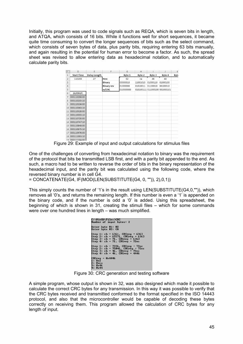
45
Initially, this program was used to code signals such as REQA, which is seven bits in length, and ATQA, which consists of 16 bits. While it functions well for short sequences, it became quite time consuming to convert the longer sequences of bits such as the select command, which consists of seven bytes of data, plus parity bits, requiring entering 63 bits manually, and again resulting in the potential for human error to become a factor. As such, the spread sheet was revised to allow entering data as hexadecimal notation, and to automatically calculate parity bits.
Figure 29: Example of input and output calculations for stimulus files
One of the challenges of converting from hexadecimal notation to binary was the requirement of the protocol that bits be transmitted LSB first, and with a parity bit appended to the end. As such, a macro had to be written to reverse the order of bits in the binary representation of the hexadecimal input, and the parity bit was calculated using the following code, where the reversed binary number is in cell G4. = CONCATENATE(G4, IF(MOD(LEN(SUBSTITUTE(G4, 0, "")), 2),0,1)) This simply counts the number of ‘1’s in the result using LEN(SUBSTITUTE(G4,0,"")), which removes all ‘0’s, and returns the remaining length. If this number is even a ‘1’ is appended on the binary code, and if the number is odd a ‘0’ is added. Using this spreadsheet, the beginning of which is shown in 31, creating the stimuli files – which for some commands were over one hundred lines in length – was much simplified.
Figure 30: CRC generation and testing software
A simple program, whose output is shown in 32, was also designed which made it possible to calculate the correct CRC bytes for any transmission. In this way it was possible to verify that the CRC bytes received and transmitted conformed to the format specified in the ISO 14443 protocol, and also that the microcontroller would be capable of decoding these bytes correctly on receiving them. This program allowed the calculation of CRC bytes for any length of input.
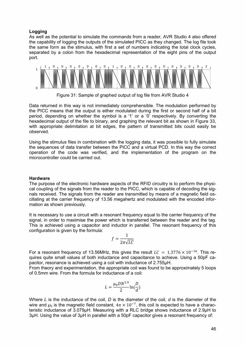
46
Logging As well as the potential to simulate the commands from a reader, AVR Studio 4 also offered the capability of logging the outputs of the simulated PICC as they changed. The log file took the same form as the stimulus, with first a set of numbers indicating the total clock cycles, separated by a colon from the hexadecimal representation of the eight pins of the output port.
Figure 31: Sample of graphed output of log file from AVR Studio 4
Data returned in this way is not immediately comprehensible. The modulation performed by the PICC means that the output is either modulated during the first or second half of a bit period, depending on whether the symbol is a ‘1’ or a ‘0’ respectively. By converting the hexadecimal output of the file to binary, and graphing the relevant bit as shown in Figure 33, with appropriate delimitation at bit edges, the pattern of transmitted bits could easily be observed. Using the stimulus files in combination with the logging data, it was possible to fully simulate the sequences of data transfer between the PICC and a virtual PCD. In this way the correct operation of the code was verified, and the implementation of the program on the microcontroller could be carried out. Hardware The purpose of the electronic hardware aspects of the RFID circuitry is to perform the physi-cal coupling of the signals from the reader to the PICC, which is capable of decoding the sig-nals received. The signals from the reader are transmitted by means of a magnetic field os-cillating at the carrier frequency of 13.56 megahertz and modulated with the encoded infor-mation as shown previously. It is necessary to use a circuit with a resonant frequency equal to the carrier frequency of the signal, in order to maximise the power which is transferred between the reader and the tag. This is achieved using a capacitor and inductor in parallel. The resonant frequency of this configuration is given by the formula:
� =1
2�√��
For a resonant frequency of 13.56MHz, this gives the result �� = 1.3776 × 10���. This re-quires quite small values of both inductance and capacitance to achieve. Using a 50pF ca-pacitor, resonance is achieved using a coil with inductance of 2.755µH. From theory and experimentation, the appropriate coil was found to be approximately 5 loops of 0.5mm wire. From the formula for inductance of a coil:
� =����
�.�
2ln(
�
�)
Where L is the inductance of the coil, D is the diameter of the coil, d is the diameter of the
wire and µ0 is the magnetic field constant, 4� × 10��, this coil is expected to have a charac-teristic inductance of 3.079µH. Measuring with a RLC bridge shows inductance of 2.9µH to 3µH. Using the value of 3µH in parallel with a 50pF capacitor gives a resonant frequency of:
1 0 0 0 0 0 0 0 1 0 0 0 0 0 0 0 0 0 0 E
0
1
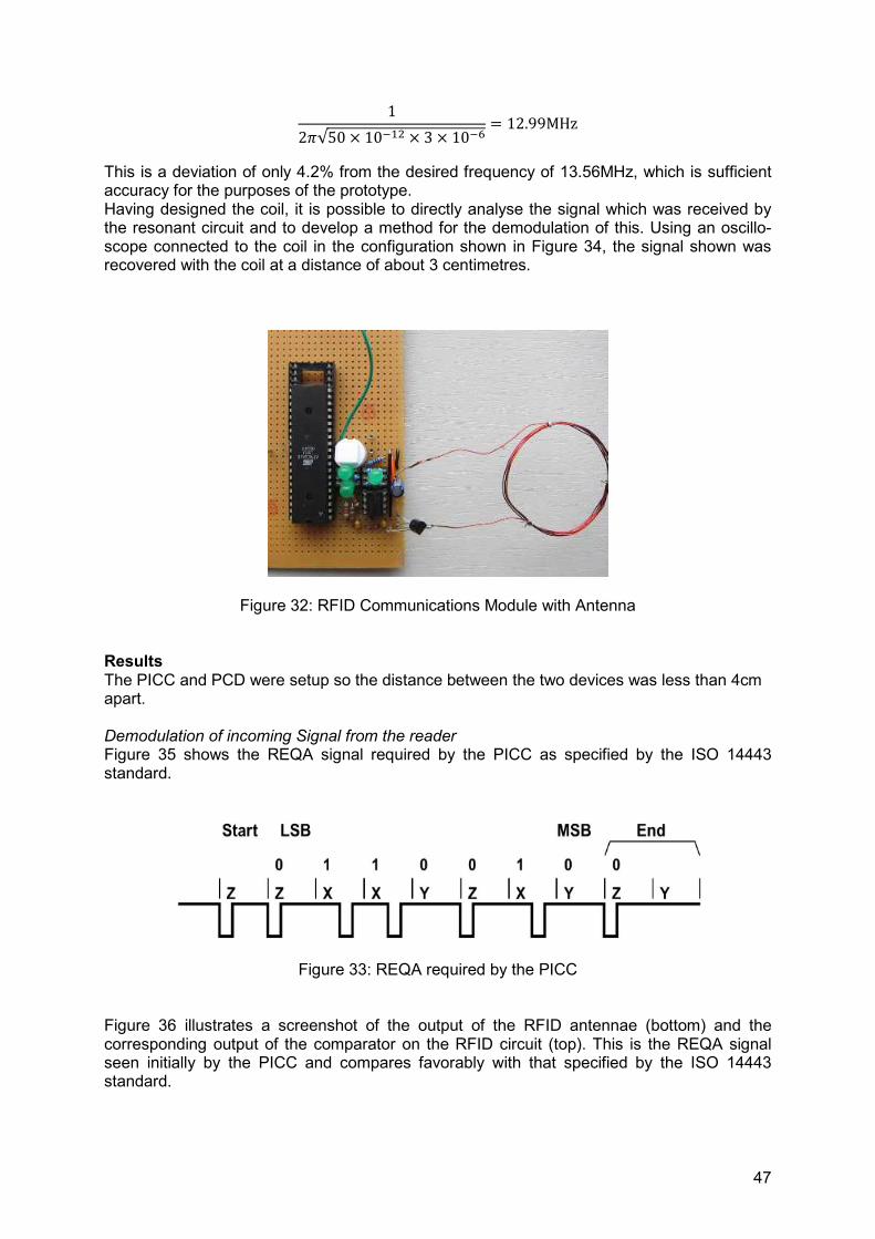
47
1
2�√50 × 10�� × 3 × 10��= 12.99MHz
This is a deviation of only 4.2% from the desired frequency of 13.56MHz, which is sufficient accuracy for the purposes of the prototype. Having designed the coil, it is possible to directly analyse the signal which was received by the resonant circuit and to develop a method for the demodulation of this. Using an oscillo-scope connected to the coil in the configuration shown in Figure 34, the signal shown was recovered with the coil at a distance of about 3 centimetres.
Figure 32: RFID Communications Module with Antenna Results The PICC and PCD were setup so the distance between the two devices was less than 4cm apart. Demodulation of incoming Signal from the reader Figure 35 shows the REQA signal required by the PICC as specified by the ISO 14443 standard.
Figure 33: REQA required by the PICC Figure 36 illustrates a screenshot of the output of the RFID antennae (bottom) and the corresponding output of the comparator on the RFID circuit (top). This is the REQA signal seen initially by the PICC and compares favorably with that specified by the ISO 14443 standard.

48
Figure 34: Output of the RFID antennae and corresponding comparator output
PICC Output Figure 37 illustrates the request acknowledge as received on the RFID antennae (Top) and the response on the output pin of the PICC (bottom). The 18 bits shown correspond to the ATQA (Answer to query) which encompasses the anti-collision protocol. This shows the intial handshaking between the PICC and the reader was successful.
Figure 35: REQA
Figure 38 highlights the period (1.258us) of the modulation is correct which illustrates the timing of the assembly code is working in practice.
Figure 368: Period of the modulation

49
Signal Response from tag as measured at the reader Figure 39 shows the signal response from the tag as measured at the reader. A clock at 1/16th of the carrier frequency is also shown. As seen in the figure when the clock is high the 13.56MHz signal gets loaded. The signal response is subsequently decoded by the reader which completes the duplex transmission of information.
Figure 379: Signal response from tag as measured at the reader
3.3.4 Implementation in Practice
It is important for the condition monitoring system to be easily incorporated into a wide variety of computer architectures. Within a desktop/laptop, there are a variety of possible configurations of hardware, owing to the number of different manufacturers and possible applications of PCs. However, the PCI bus is a standard feature of the vast majority of PCs, and has proven to be very resistant to the changes that computer architectures are constantly undergoing. While the PCI card has changed somewhat since it was introduced, compatibility has been maintained between the current standard and previous ones. This suggests that the PCI bus is likely to be similarly robust to future change, and that it will remain a feature of PCs for the foreseeable future. A further advantage of the PCI card as a development platform is that one end of the card is external to the PC, allowing the location of the RFID antenna on the outside of the case, preventing magnetic interference from the metal case. A conceptual illustration of the hardware on a PCI card is shown in Figure 40. The microcontroller generates the interrupt that requests lifecycle information from the CPU and other primary system components containing hardware sensing devices. It is also involved in data reduction on the lifecycle information generated by each respective component and again in RFID communications. The compressed lifecycle information is stored in the EEPROM before transfer to the reader.
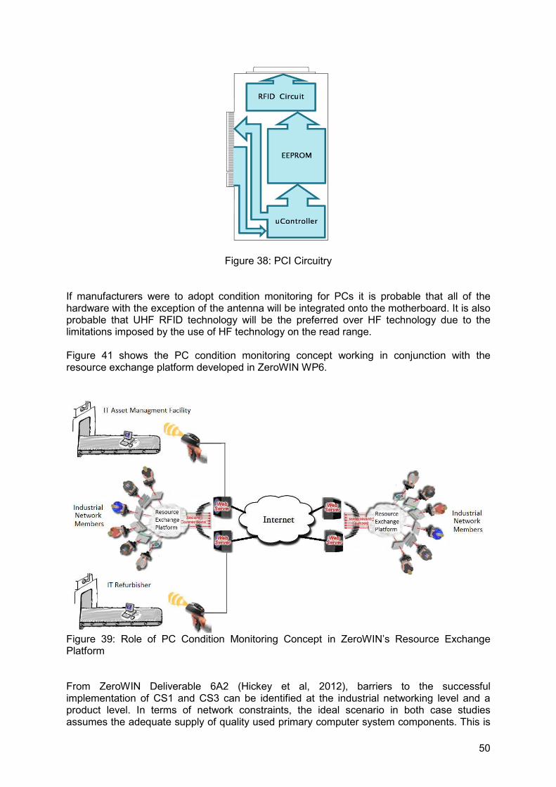
50
Figure 38: PCI Circuitry If manufacturers were to adopt condition monitoring for PCs it is probable that all of the hardware with the exception of the antenna will be integrated onto the motherboard. It is also probable that UHF RFID technology will be the preferred over HF technology due to the limitations imposed by the use of HF technology on the read range. Figure 41 shows the PC condition monitoring concept working in conjunction with the resource exchange platform developed in ZeroWIN WP6.
Figure 39: Role of PC Condition Monitoring Concept in ZeroWIN’s Resource Exchange Platform From ZeroWIN Deliverable 6A2 (Hickey et al, 2012), barriers to the successful implementation of CS1 and CS3 can be identified at the industrial networking level and a product level. In terms of network constraints, the ideal scenario in both case studies assumes the adequate supply of quality used primary computer system components. This is

51
essentially an issue of reverse logistics, where supply uncertainties in terms of quality, timing, and quantity of returned products are issues that can impact the feasibility of the proposed concept. At a product level, quality is a key issue. This issue arises from the lack of information associated with the returned products. The PC condition monitoring concept demonstrated can serve to addresses information asymmetries concerning used primary system components between IT asset management firms/Refurbishers and computer manufacturers.
3.4 Concepts based on programmable logic to enable reuse of products
The following sections introduce the concept of modular digital electronic circuits based on programmable logic device (PLD) technology. The proposed concept is that the functional electronic units can be reused at EOL to perform a similar task in a different system or different industry. This may be viewed as an ecodesign methodology that can be employed for industrial networks to increase environmental efficiency when dealing with complex low entropy products,typically electronics sub-assemblies.
3.4.1 Methodology
A diagram outlining a typical product life cycle where environmental considerations have been taken at the design stage is shown in Figure 42. For this product the ecodesign strategy incorporates the re-use of subsystems in future products from the same generation and also in future generations of products.
Figure 40: Eco-design Methodology for Enabling Industrial Networking of Electronic Products and Assemblies

52
There are a number of important aspects which must be examined in order to ensure that this can be implemented successfully. The first of these aspects is the design stage. As illustrated in Figure 1, there must be interconnectivity at a design level between the various product iterations as it is necessary for product designers within the industrial network to consider future generations of products as well as previous generations. In consideration of other products at the design stage it is required to incorporate electronic systems with sufficient functional capabilities and flexibility to be of use in other products within the industrial networks. Whereas this may be at the burden of some additional cost initially (but not necessarily), a life cycle costing approach should more than compensate for it. Considering previous designs is also essential to ensure that these systems actually get incorporated in the latest version as any environmental benefit is forfeited unless this takes place. Potentially, upon larger adoption of the scheme in industrial networks, designers should also give consideration to suitable programmable logic device (PLD) based systems that may be available from take back schemes involving other products. The next aspect for consideration is the use phase and more specifically the reliability of the re-used systems. Systems based entirely on solid-state devices are particularly suited to re-use as their reliability profile is described in terms of a bathtub curve shown in Figure 43.
Figure 41: The Bathtub Curve
This profile represents a failure probability that is relatively high in early life, known as burn-in, due to intrinsic material or process defects, before entering a long period of very high reliability. The typical lifetime of consumer electronics, particularly mobile products, is far shorter than this period of low failure rates ensuring that reuse of semiconductor systems within these timescales is a reliable activity. Indeed, any functional aspects of an electronic system, even those of PLD systems, will most likely be redundant in the case of the system reaching the end of life wearing out point on the bathtub curve where the failure probability increases again. The final issue with respect to the successful implementation of such a scheme is the feedback loop from end of life to (re)manufacture. In an unregulated market the economic factors associated with take back would make it an unlikely strategy to pursue. However, with radio frequency identification (RFID) (which has been shown to be technically feasible for deployment in industrial networks in D2.1) it can lead to the development of a reverse logistics infrastructure that can make the above concept realisable. Utilities like resource exchange platform being developed in ZeroWIN WP6 can serve to further auger the success of adoption.
3.4.2 Technology

53
There are many technologies available today used to build digital circuits. Digital Signal Processors (DSPs) are designed specifically for signal processing in real time. Standard microprocessors can also perform DSP, but in general DSPs are usually dedicated integrated circuits (ICs). Another type of IC used to build digital circuits are called Programmable Logic Device (PLDs), a PLD has an undefined function when manufactured and the function can be programmed into the IC at a later stage unlike a fixed function logic gate IC. The main types available are shown in Figure 44.
Figure 42: Programmable Device Types PLDs were invented in the late seventies and since then they have proved to be very popular, so much that they are now one of the largest growing sectors in the semiconductor industry. If a manufacturer is looking for a lower risk route into customized silicon a PLD can be used, for small to medium volume production, or where a higher volume but Fast Time To Market (TTM) is required. PLDs can provide designers with greater flexibility, design integration and can be easily reprogrammed to upgrade system functionality. Today, the use of high performance PLDs is persuasive in industrial electronic system design application. The ability to configure and readily modify complex digital circuits and systems provides many time and cost advantages. Such devices also provide a good example of how over the last number of years, the line between hardware and software has blurred. With electronic hardware design engineers creating the bulk of their new digital circuitry in programming languages such as VHDL and Verilog- HDL and often target it to programmable logic, this is changing the way electronic systems are designed. In simple terms, a single PLD can replace a PCB containing multiple COTS discrete digital ICs, providing a potentially smaller and faster solution with lower power consumption. However, the devices have more use for their ability to rapidly prototype complex Application Specific Integrated Circuit (ASIC) designs through to in-system upgrading via a local programme or remotely via the Internet as shown in figure 45 .
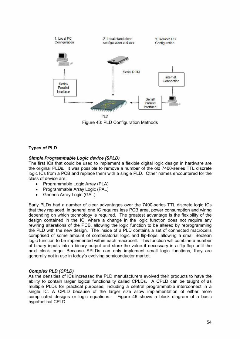
54
Figure 43: PLD Configuration Methods
Types of PLD Simple Programmable Logic device (SPLD) The first ICs that could be used to implement a flexible digital logic design in hardware are the original PLDs. It was possible to remove a number of the old 7400-series TTL discrete logic ICs from a PCB and replace them with a single PLD. Other names encountered for the class of device are:
• Programmable Logic Array (PLA)
• Programmable Array Logic (PAL)
• Generic Array Logic (GAL) Early PLDs had a number of clear advantages over the 7400-series TTL discrete logic ICs that they replaced, in general one IC requires less PCB area, power consumption and wiring depending on which technology is required. The greatest advantage is the flexibility of the design contained in the IC, where a change in the logic function does not require any rewiring alterations of the PCB, allowing the logic function to be altered by reprogramming the PLD with the new design. The inside of a PLD contains a set of connected macrocells comprised of some amount of combinatorial logic and flip-flops, allowing a small Boolean logic function to be implemented within each macrocell. This function will combine a number of binary inputs into a binary output and store the value if necessary in a flip-flop until the next clock edge. Because SPLDs can only implement small logic functions, they are generally not in use in today’s evolving semiconductor market. Complex PLD (CPLD) As the densities of ICs increased the PLD manufacturers evolved their products to have the ability to contain larger logical functionality called CPLDs. A CPLD can be taught of as multiple PLDs for practical purposes, including a central programmable interconnect in a single IC. A CPLD because of the larger size allow implementation of either more complicated designs or logic equations. Figure 46 shows a block diagram of a basic hypothetical CPLD

55
Figure 44: Internal structure of a CPLD.
The logic blocks that correspond to one SPLD, each comprised of macrocells and interconnect wiring like an ordinary SPLD, but the switch matrix in a CPLD might not be fully connected unlike the programmable interconnect within a SPLD. The problem with this is that some of the possible connections between logic block outputs and inputs may not actually be included within the CPLD, making 100 per cent utilisation of the macrocells very difficult to achieve. If there are sufficient logic gates and flip-flops available, some hardware designs will not fit within the CPLD. Field Programmable Gate Array (FPGA) A FPGA is a device that can be used to implement any digital hardware design, prototyping of ASIC hardware is one common use, and a designer has the option to use the FPGA in the final manufactured product. The initial costs associated with the development of an ASIC can be high, but in the long run the cost per IC may be cheaper than a FPGA. The FPGA has a different architecture than the CPLD, and this can be seen when looking at the basic internal architecture. Figure 47 illustrates a typical FPGA architecture
Figure 45: Internal structure of a FPGA
The structure of a FPGA can be grouped into 3 blocks, programmable interconnect, core logic blocks and I/O logic blocks, the perimeter around the device contains the big I/O logic, each providing programmable access to the input, output, or by directional general purpose package I/O pins on the device. Contained within the device is an array of core logic blocks,

56
and the programmable interconnections between core logic blocks to core logic blocks and the I/O. The core logic blocks within the device are relatively small and simple, on the other hand the macrocells in a CPLD are far more complex, but because of the amount of core logic blocks there are a far greater number of flip-flops, which means that the architecture of a FPGA is far more flexible than a CPLD. Crucially, for their use in industrial networks, it is possible to configure any of the pins in any manner desirable. i.e., any pin can be an input or an output depending on the application required. This inherent flexibility makes FPGA’s the most adaptable of all integrated electronics and the choice for industrial networking.
3.4.4 Design Examples
The use of digital PL in the design and development of reconfigurable electronic systems that can be used to extend the lifespan of an electronic product or circuit board are investigated in this section. Utilising PL within a suitably defined electronic system, the same electronics can be configured to adapt to new end-user requirements. This permits the development of generic electronic platforms ranging from the simple to the high-functionality that when appropriately configured, can be used in a diverse range of end-user applications. A review of the available PL technologies matching their capabilities to potential design applications was undertaken. The PLD needs to contain sufficient functional capabilities to carry out all of the tasks required while still being cost efficient to be considered in evolving generations of the designs or completely different designs. A number of products with a range of turnover times and the requirements for each product are identified in table 6.
Design
Product Turnover
Examples
Technologies Employed
1
18 Months – 2
Years.
Mobile Phones,
Microprocessors, Memory
(SRAM,Flash, EPROM),
DSP
2
3 – 5 Years.
Audio Hi-fi
Memory, DSP,
3
Greater than 5
Years.
Washing
Machines,
Embedded State Machine
Designs (Hardware or
Software)
Table 6: Application Designs Considered
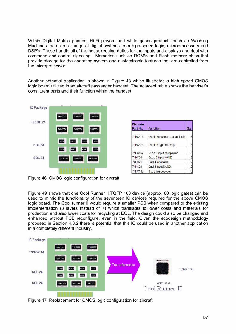
57
Within Digital Mobile phones, Hi-Fi players and white goods products such as Washing Machines there are a range of digital systems from high-speed logic, microprocessors and DSP’s. These handle all of the housekeeping duties for the inputs and displays and deal with command and control signaling. Memories such as ROM’s and Flash memory chips that provide storage for the operating system and customizable features that are controlled from the microprocessor.
Another potential application is shown in Figure 48 which illustrates a high speed CMOS logic board utilized in an aircraft passenger handset. The adjacent table shows the handset’s constituent parts and their function within the handset.
Figure 46: CMOS logic configuration for aircraft Figure 49 shows that one Cool Runner II TQFP 100 device (approx. 60 logic gates) can be used to mimic the functionality of the seventeen IC devices required for the above CMOS logic board. The Cool runner II would require a smaller PCB when compared to the existing implementation (3 layers instead of 7) which translates to lower costs and materials for production and also lower costs for recycling at EOL. The design could also be changed and enhanced without PCB reconfigure, even in the field. Given the ecodesign methodology proposed in Section 4.3.2 there is potential that this IC could be used in another application in a completely different industry.
Figure 47: Replacement for CMOS logic configuration for aircraft

58
3.5 Evaluation of EOL levels according to the technology concepts
Table 7 summarizes the technology concepts and shows possible impacts for the different steps in EOL. These steps include collection, transportation, data elaboration, materials flow, handling processing and management.
collection transportation data elaboration
materials flow
handling/ processing
management
RFID active + + ++ o - ++
RFID passive
++ + ++ + o ++
Monitoring system extern
+ o ++ - - +
Monitoring system intern
- o ++ - - +
--: high negative impact, -: negative impact, o: no impact, +: impact, ++: high positive impact
Table 7: Potential for the Integration in EOL systems The table compares the impacts at EOL of the condition monitoring technology concepts proposed in Section 3.2 and 3.3 with the impacts at EOL of active and passive RFID technologies. In the case of active RFID, positive impacts are seen across all EOL stages with the exception of materials flow (no impact) and handling/processing. Active RFID represents a negative impact for handling/processing as the technology must be removed from the electronics sub-assembly prior to this step. This contrasts with passive RFID which does not negatively impact EOL processing to the same degree. External and internal condition monitoring concepts have both similar implications across the transportation, data elaboration, materials flow, handling processing and management EOL stages. No impact is incurred in transportation for both types of technology. While positive impacts are true for both again in terms of data elaboration and management, negative impacts are incurred for materials flow and handling/processing. However, external condition monitoring is advantageous over internal condition monitoring during the collection stage.
4. SUMMARY The hypothesis that waste is materials that is useless and unwanted because no information and knowledge about it is available, has been introduced and suggested in this report. Based on this hypothesis technical concepts have been suggested. The introduced technical possibilities try to engage separate industries in a collective approach to competitive advantage involving physical exchange of materials, energy, water, and by-products. The focus has been set on collaboration and synergistic possibilities offered by geographic proximity. A general understanding of useful tools and approaches has been discussed. The following aspects have been considered in the explored tools:
� Condition monitoring of products and processing units � Input-output matching � Material identification and tracking � Communication (internal and external) � Logistic and transport monitoring � Optimization and design of industrial networks

59
Possible technical solutions have been discussed to establish either a stream-based or a business-based reuse of products in industrial networks. The stream-based reuse accounts the material and energy in the planning of industrial networks. A business-based approach foremost considers the network institution in the reuse planning. The enormous potential of using information technology for environmental improvement through reuse in industrial network has been illustrated. It starts with the industrial single process and leads to the chain of processes inside one manufacturer or by cross linking of materials, products and by-products between different manufacturers. The report can be used as a feasibility study of how technology could enhance the reuse in the industry. The challenges facing the reuse are introduced. On the basis of these technical challenges, potential solutions are developed. Through these solutions, the problem of reuse can be better understood. The exemplary solutions suggest that the technology introduced in the report can help to make a step forward into the next generation of industrial networks. A summary of the technology concepts developed are as follows: A modular hardware concept based on embedding of passive and active components in various stacks with standardized communication protocol between the different stacks has the potential to fulfill variable demands from several case studies. The Implementation of various energy harvesters to create autonomous micro systems enables in combination with wireless network communication the monitoring of sensor data in harsh environments and on difficult to reach places. IGBT are the back bone of modern power electronics. The condition monitoring of such devices is crucial for all energy infrastructures now and in the future. A concept for the photovoltaic industry is developed together with the Zerowin partner TTA and will be implemented and tested in the next time. Computer condition monitoring utilizing existing hardware sensing technologies within systems has been demonstrated at a proof of concept level. This is applicable CS1 and CS3 in ZeroWIN. The system utilises thermal sensors already present in the components of a computer system to track the health of the computer throughout its lifetime. At EOL, this data can be extracted using RFID to allow a fast first diagnosis of the reuse potential of the system. The choice of RFID as a suitable technology, the requirements of the MIFARE RFID standard, and the modifications made to the standard to allow the transmission of the volumes of data required for lifetime condition monitoring has been investigated. The method of data reduction in use for thermal data, and the location of the system on the PCI bus of the PC have also been examined. As demonstrated in Section 3.4, PLDs are a technology that is eminently suitable to increase reuse in industrial networks. When utilising PLD technology, the internal hardware configuration (circuit) is changed rather than the external printed circuit board design. It was also described how a modular card containing a state-of-the-art PLD can be used in various generations of a product or in a completely different application. This has the benefits in that the PCB only needs to be designed and manufactured once and when the design is to be upgraded or the functionality changed, then the configuration of the PLD is changed via a software program running on a programmer PC. The designs described conform with the Eco-Design principles of modularity, upgradability and re-usability, and are suitable for use in a multitude of applications from the simple to the high functionality with no re-use bottlenecks associated with microprocessor based circuit boards. The report has illustrated the mentioned techniques in exemplary solutions in different fields. These specific solutions represent a possible use of the technology to ensure the philosophy

60
behind the industrial symbiosis. The exemplary solutions are based on case studies of the ZeroWin project. This report contends that end-of-pipe treatment techniques do not actually eliminate the waste but simply transfer it from one environmental medium to another. The key factor to solve this problem is to have information and knowledge about the waste. It is likely that, as further restrictions are placed on the disposal of substances to environmental media, the costs of treatment and disposal of substances continue to rise. This report will suggest possible techniques, which had already reached a state of the art that can change the way of thinking about the end-of-pipe treatment. It is now possible to transfer unnecessary output material and by-product from one company environment to another. The report will enable decision makers in the industry to settle on whether to use the technical possibilities and go forward in the planning of reuse in industrial networks or not. Reuse is therefore a strategy and comprises one of the most important components of a company’s environmental management system.

61
5. REFERENCES Benecke, S., Rueckschloss,J., Middendorf, A., Nissen, N. F., Lang, K.-D., Energy Harvesting for Distributed Microsystems – The Link between Environmental Performance and Availability of Power Supply, ECODESIGN, Japan, 2011 Chertow, M., Uncovering industrial symbiosis, Journal of Industrial Ecology, 11(1): 11–30, 2007 Cole, D. Energy consumption and personal computers. In Computers and the Environment-Understanding and Managingtheir Impacts; Ruediger, K., Williams, E., Eds.; Kluwer Academic Publishers: London, 2004; p 154. Gabriel B. Grant, Thomas P. Seager Guillaume Massard and Loring Nies, Information and Communication Technology for Industrial Symbiosis, Center for Industrial Ecology, Yale University, 2010 Gasperi, M. L. Life Prediction Model for Aluminum Electrolytic Capacitors. IEEE Industry Applications Conference1996 GEC 2008. "Closing the Loop : Electronics Design to Enhance Reuse/Recycling Value Discussion Draft Report," Green Electronics Council in collaboration with the National Center for Electronics Recycling and Resource Recycling, Inc., 2008, September. Goel, A.; Graves, R. J. Electronic system reliability: collating prediction models IEEE Trans. Device Mater Reliab. 2006, 6 (2). Lall, P.; Pecht, M. G.; Hakim, E. B. Influence of Temperature onMicroelectronics and System Reliability; CRC Press: Boca Raton,FL, 1997. Linc IT. PC Shutdown-to Be or Not to Be; Commonwealth Department of Primary Industries and Energy, 1995. Mercer, K., et al“Does Power Cycling a Desktop Computer harm it?” A review of the literature, ” New Zealand Energy Efficiency and Conservation Authority, www.energywise.co.nz/content/ ew_business/office_equipment/Power_Cycling.html, Accessed01-02-09. Nelson L. Nemerow, Zero Pollution for Industry, A Wiley-Interscience Publication, 1995 Noel Brings Jacobsen, Voraussetzungen für eine erfolgreiche industrielle Symbiose, Industrial Ecology: Erfolgreiche Wege zu nachhaltigen industriellen Systemen, Vieweg Teubner, 2007 Paparrizos, G. Detecting Failure in DC Cooling Fan 2005,http://www.electronicproducts.com/ShowPage.asp?FileName)microchip.may2005.HTML (Accessed 01-02-08). Pinheiro, E.; Weber, W. D.; Barroso, L. A. Failure Trends in a Large Disk Drive Population; 5th USENIX Conference on File and Storage Technologies (FAST):, 2007,San Jose, CA. Vichare, N. M.; Pecht,M.G. Prognostics and health management of electronics. IEEE Trans Compon., Packag. Technol. 2006, 29(1), 222–229.

62
Seagate1999 GetSMART for Reliability; Seagate Technology, Inc.: Scotts Valley,CA, 1999. Silicon Systems, 2005 Increasing Flash Solid State Disk Reliability; 2005, http://www.storagesearch.com/siliconsys-art1.html, Accessed (28-10-10).
63
6. GLOSSARY OF SYMBOLS AND ABBREVIATIONS ASIC Application Specific Integrated Circuit ATQA Answer to Request CPLD Complex Programmable Logic Device CPU Central Processing Unit CRC Cyclic Redundancy Check CMOS complementary-symmetry metal–oxide semiconductor EEPROM Electrically erasable programmable read-only memory EOL end-of-life FPGA Field Programmable Gate Array GAL Generic Array of Logic GEC Green Electronics Council HDD Hard Disk Drive HDL Hardware Description Language HF High Frequency ISO International standards Organization I/O Input/Output KB kilobyte MB motherboard MHz megahertz NVB Number of Valid Bits PAL Programmable Array of Logic PC Personal Computer PCD Proximity Control Device PCI Peripheral Component Inter-connect PDF Probability density Function PICC Proximity Integrated circuit card PL Programmable Logic PLA Programmable Logic Array REQA Request Command Type A RFID Radio Frequency Identification SD Standard Definition SEL Select Command SMART Self-Monitoring and Reporting Technology SPLD Simple Programmable Logic Device SSD Solid State Drive TTM Time to Market UHF Ultra High Frequency UID Unique Identification

64
VHDL Verilog Hardware Description Language WUP wakeup oC degrees celcius