delivering next generation technology series ......delivering next generation technology series...
TRANSCRIPT

Page 1 of 18
Delivering Next Generation Technology
Series
FPLR36T5R010NJ 19.2-60Vdc Input, 10A, 5-18Vdc Output
http://www.fdk.co.jp Ver 1.1 Dec. 25, 2013
Preliminary Datasheet
The FPLR36T5R010NJ converter of the Series operates from 19.2Vdc-60Vdc wide input, and delivers 10A of output current at a tightly regulated programmable output voltage of 5Vdc to 18Vdc. The thermal performance is excellent.
シリーズの FPLR36T5R010NJはワイド入力電圧範囲 19.2Vdc~
60Vdcで動作し、高精度でプログラム可能な出力電圧5Vdc~18Vdcで、
10Aの出力電流を供給します。また、温度特性が非常に優れています。
This leading edge thermal performance results from electrical, thermal and packaging design that is optimized for high density circuit card conditions. Extremely high quality and reliability are achieved through advanced circuit and thermal design techniques and FDK’s state of the art in-house manufacturing processes and systems.
回路設計、放熱設計、及びパッケージング設計の結果である、この最先端
の温度特性は、高密度実装回路用に最適化されています。非常に優
れた品質と信頼性は高度な回路設計、温度設計技術、及びFDKの最
先端の自社製造プロセスによりもたらされます。
Applications
Amusement/Gaming Machines アミューズメント/ゲーム機器
Factory Automation FA機器
Connections
Features Compliant to RoHS EU Directive 2011/65/EC
RoHS 2011/65/EU 適合 Delivers up to 10A (180W)
10A (180W)まで供給可能 High efficiency, 95%peak at 36Vin, 12Vout
高効率-放熱器が不要 Small size and low profile:1.681” x 0.760” x 0.512”
小型、低背 (42.7 x 19.3 x 13.0mm) SIP pin-out
SIPピンレイアウト Remote ON/OFF, Negative logic
リモートON/OFFはネガティブロジック Programmable output voltage via external resistor
外部接続の抵抗によりプログラム可能な出力電圧
Start up into pre-biased output 出力にプリバイアスがあっても起動可能
Auto-reset output over-current protection 過電流保護機能: 自動復帰
Auto-reset output over-temperature protection 内部加熱保護機能
High reliability, MTBF = 1 Million Hours 高信頼性: MTBF = 1 Million 時間
UL60950 compliant UL60950とIEC/EN60950 準拠
All materials meet UL94, V-0 flammability rating 全ての部品は UL94 V-0に適合
FPLR36T5R010*J

Page 2 of 18
Delivering Next Generation Technology
Series
FPLR36T5R010NJ 19.2-60Vdc Input, 10A, 5-18Vdc Output
http://www.fdk.co.jp Ver 1.1 Dec. 25, 2013
Preliminary Datasheet
Electrical Specifications 電気的仕様 All specifications apply over specified input voltage, output load, and temperature range, unless otherwise noted. 注記が無い場合、全ての仕様は指定された入力電圧、負荷、温度範囲で適用されます。 Conditions: Ta=25degC, Airflow=200LFM (1.0m/s), Vin=36Vdc, Vout=5-18Vdc, unless otherwise specified.
1Absolute Maximum Ratings 絶対最大定格 Stresses in excess of the absolute maximum ratings may lead to degradation in performance and reliability of the converter and may result in permanent damage. 絶対最大定格を超えたストレスは、性能の低下、長期信頼性の低下、及びモジュールの破損を引き起こすことがあります。
PARAMETER NOTES MIN TYP MAX UNITS
ABSOLUTE MAXIMUM RATINGS1
Input Voltage Continuous -0.3 60 Vdc
Operating Temperature Ambient temperature -40 85 °C
Storage Temperature -55 125 °C
Output Voltage 5 18 Vdc
FEATURE CHARACTERISTICS
Switching Frequency 350 kHz
Output Voltage Programming Range By external resistor. See trim table-1 5 18 Vdc
Remote Sense Compensation 0.5 Vdc
Turn-On Delay Time Full resistive load
with Vin (module enabled, then Vin applied) From Vin=Vin(min) to 0.1*Vout(nom) 5 ms
with Enable (Vin applied, then enabled) From enable to 0.1*Vout(nom) 5 ms
Rise Time (Full resistive load) From 0.1*Vout(nom) to 0.9*Vout(nom) 5 ms
ON/OFF Control (Negative)
Module Off 2.4 12 Vdc
Module On -5 0.8 Vdc

Page 3 of 18
Delivering Next Generation Technology
Series
FPLR36T5R010NJ 19.2-60Vdc Input, 10A, 5-18Vdc Output
http://www.fdk.co.jp Ver 1.1 Dec. 25, 2013
Preliminary Datasheet
Electrical Specifications (Continued) 電気的仕様 (続き) Conditions: Ta=25degC, Airflow=200LFM (1.0m/s), Vin=36Vdc, Vout=5-18Vdc, unless otherwise specified.
PARAMETER NOTES MIN TYP MAX UNITS
INPUT CHARACTERISTICS
Operating Input Voltage Range Vout≦ 15Vdc 19.2 60 Vdc
15Vdc < Vout ≦ 18Vdc 23.0 60 Vdc
Input Under Voltage Lockout
Turn-on Threshold 17.0 Vdc
Turn-off Threshold 14.5 Vdc
External Input Capacitance 47 100 uF
Maximum Input Current 10Adc out at 36Vdc in
Vout=18Vdc 5.3 Adc
Vout=12Vdc 3.6 Adc
Vout=5Vdc 1.6 Adc
Input Stand-by Current (module disabled) 10 mA
Input No Load Current Vout=18Vdc 55 mA
Vout=12Vdc 50 mA
Vout=5Vdc 30 mA
Input Reflected-Ripple Curren See Fig. G for setup (BW=20MHz) mAp-p
Vout=18Vdc 84 mAp-p
Vout=12Vdc 78 mAp-p
Vout=5Vdc 50 mAp-p

Page 4 of 18
Delivering Next Generation Technology
Series
FPLR36T5R010NJ 19.2-60Vdc Input, 10A, 5-18Vdc Output
http://www.fdk.co.jp Ver 1.1 Dec. 25, 2013
Preliminary Datasheet
Electrical Specifications (Continued) 電気的仕様 (続き) Conditions: Ta=25degC, Airflow=200LFM (1.05m/s), Vin=36Vdc, Vout=5-18Vdc, unless otherwise specified.
PARAMETER NOTES MIN TYP MAX UNITS
OUTPUT CHARACTERISTICS Output Voltage Set Point (no load) -1.5 Vout +1.5 %Vout
Output Regulation
Over Line Full resistive load +/- 0.1 %Vout
Over Load From no load to full load +/- 0.4 %Vout
Output Voltage Range (Over all operating input voltage, resistive load and temperature conditions until end of life)
-3.0 +3.0 %Vout
Output Ripple and Noise BW=20MHz Over line, load and temperature (Fig. F)
Peak to Peak Vout=18Vdc 180 270 mVp-p
Peak to Peak Vout=12Vdc 100 150 mVp-p
Peak to Peak Vout=5Vdc 30 45 mVp-p
External Load Capacitance Plus full load (resistive)
Min ESR > 1mΩ 330 820 uF
Output Current Range 0 10 A
Output Current Limit Inception (Iout) Vout=5 Vdc 15.7 A
Output Short-Circuit Current Short=10mΩ, Vout=5 Vdc set 2.4 Arms
DYNAMIC RESPONSE
Iout step from 5A to 10A with di/dt= 0.1A/uS Co=330uF x 1 aluminum + 1uF ceramic 300 mV
Setting time (Vout < 10% peak deviation) 150 μS
Iout step from 10A to 5A with di/dt= 0.1A/uS Co=330uF x 1 aluminum + 1uF ceramic 300 mV
Setting time (Vout < 10% peak deviation) 200 μS
EFFICIENCY Full load (10A)
Vout=18Vdc 96.0 %
Vout=12Vdc 95.0 %
Vout=5Vdc 90.0 %

Page 5 of 18
Delivering Next Generation Technology
Series
FPLR36T5R010NJ 19.2-60Vdc Input, 10A, 5-18Vdc Output
http://www.fdk.co.jp Ver 1.1 Dec. 25, 2013
Preliminary Datasheet
Operation Input and Output Impedance The FPLR36T5R010*J converter should be connected to a DC power source using a low impedance input line. In order to counteract the possible effect of input line inductance on the stability of the converter, the use of decoupling capacitors placed in close proximity to the converter input pins is recommended. This will ensure stability of the converter and reduce input ripple voltage. Although low ESR Tantalum or other capacitors should typically be adequate, very low ESR capacitors (ceramic, over 47uF) are recommended to minimize input ripple voltage. The converter itself has on-board internal input capacitance of 10uF with very low ESR (ceramic). FPLR36T5R010*Jと入力電源間は低インピーダンスで接続してください。コン
バータの安定性に影響のある入力インダクタンスを抑えるため、コンバータの入
力ピンの近傍にデカップリングコンデンサを付加することをお勧めします。これ
によりコンバータの安定動作を確実にし、入力リップル電圧を抑制します。低
ESRタンタル、又はその他のコンデンサも一般的には問題ありませんが、入
力リップルを最小にするためには、非常に低ESRコンデンサ(セラミックで47uF以
上)を推奨します。コンバータ自身は入力回路に極低ESRの10uFセラミック入
力コンデンサを搭載しています。
The FPLR36T5R010*J is capable of stable operation with no external capacitance on the output. To minimize output ripple voltage, the use of very low ESR ceramic capacitors is recommended. These capacitors should be placed in close proximity to the load to improve transient performance and to decrease output voltage ripple. FPLR36T5R010*Jは出力に外付けコンデンサが無い状態でも安定して動
作します。出力リップルを最小にするため、極低ESRのセラミックコンデンサの接
続を推奨します。過渡時の特性向上と出力リップル低減のために負荷の
近傍に極低ESRセラミックコンデンサを実装することをお勧めします。
Note that the converter has a SENSE pin to counteract voltage drops between the output pins and the load. However, the impedance of the line from the converter output to the load should thus be kept as low as possible to maintain good load regulation. このコンバータは出力端子と負荷間の電圧ドロップを補正するセンス端子を
持っています。しかし、精度の高い負荷特性を保持するために、コンバータ
の出力から負荷までのラインインピーダンスは可能な限り低くしてください。
ON/OFF (Pin 12) The ON/OFF pin (pin 12) can be used to turn the converter on or off remotely using a signal that is referenced to GND (pin 6, 7 & 8), as shown in Fig. A. To turn the converter on Pin 12 should be at logic low or left open, and to turn the converter off Pin 12 should be at logic high or connected to Vin. ON/OFF端子(12番ピン)は図Aのように、グランド(6番ピン、7番ピン、8番ピン)
を基準としたリモート信号によりコンバータをON/OFFするのに使われます。コ
ンバータをONするには12番ピンをLowレベル、又は未接続とし、コンバータを
OFFするには12番ピンをHighレベル、又はVinと接続とします。
The ON/OFF pin (pin 12) is internally pulled-down. A TTL or CMOS logic gate or an open collector (open-drain) transistor can be used to drive Pin 12. When using an open collector (open -drain) transistor, a pull-up resistor, R*=75kΩ, should be connected to Vin (See Fig.A). The device driving Pin 12 must be capable of: (b) Sinking up to 0.2mA at low logic level (≦0.8V) (c) Sourcing up to 0.25mA at high logic level (2.4–5V) (d) Sourcing up to 0.75mA when connected to Vin ON/OFFピンはモジュール内部でプルダウンされています。TTL、 CMOSロジッ
ク、又はオープンコレクタ(オープンドレイン)のトランジスタもON/OFFピンの操作に使
用可能です。オープンコレクタ(オープンドレイン)のトランジスタを使用する時は75k
Ωのプルアップ抵抗をVinに接続してください。
(図A参照) ON/OFFピンを操作するデバイスには下記能力が必要です。
(b) 0.8V以下のLowレベルで0.2mAまでのシンク能力
(c) 2.4V-5VのHighロジックレベルで0.25mAまでの供給能力
(d) Vin接続時には0.75mAまでの供給能力
Fig. A: Circuit configuration for remote ON/OFF
R* is for negative logic option only

Page 6 of 18
Delivering Next Generation Technology
Series
FPLR36T5R010NJ 19.2-60Vdc Input, 10A, 5-18Vdc Output
http://www.fdk.co.jp Ver 1.1 Dec. 25, 2013
Preliminary Datasheet
Remote Sense (Pin 4) The FPLR36T5R010*J converter incorporates a remote sense function to compensate for voltage drops between Vout (pin 1, 2 & 3) and the load. SENSE (pin 4) should be connected via a separate trace to a point close to the load or to a point where regulation is required; see Fig. B. This trace should be located in proximity to a ground plane to minimize noise pick-up. Note that GND (pin 6, 7 & 8) does not have a sense function: good connectivity to a ground plane is needed for low voltage drop.
In case the remote sense function is not required, SENSE (pin 4) must be connected to Vout (Pin 1, 2 & 3). In the absence of this connection, the converter will provide a slightly higher output voltage than that specified. FPLR36T5R010*JコンバータはVout(1, 2, 3番ピン)と負荷の間で起こる電圧
低下を補正するために、リモートセンス機能を有しています。SENSE(4番ピン)
は負荷端、又は補正が必要な箇所に個別の配線で接続してください。
(図B参照) この配線はノイズの影響を最小にするため、グランドに近接し
て配線してください。GND(6, 7, 8番ピン)はセンス機能がありませんので、
電圧低下を少なくするためにグランドに良好な接続が必要です。
リモートセンス機能が必要無い場合は、SENSE(4番ピン)はVout(1, 2, 3番ピン)
に接続してください。接続が無い場合、コンバータは出力電圧規格より若
干高い電圧を出力します。
Note that the remote sense function will allow the output voltage at Vout to be up to 0.5V above the nominal rated voltage in order to maintain regulation at the sense point. The system design should take this into account to ensure that the maximum power drawn from the converter under a given set of conditions does not exceed that allowed by the derating curves. リモートセンス機能は、センス箇所の電圧を規格内にするため、Vout端の電
圧を基準出力電圧より最大0.5V高くします。システムをデザインする際、こ
の機能に留意し、ディレーティングカーブで許容される最大電力以下で使用す
るよう、注意してください。
Output Voltage Programming (Pin 5) The output voltage of the FPLR36T5R010*J converter can be programmed from 5V to 18V by using an external resistor or a voltage source FPLR36T5R010*Jの出力電圧は外部抵抗を接続するか、又は外部電
源を印加することで 5V~18Vまで可変可能です。
External Resistor An external trim resistor, RTRIM, should be connected between TRIM (pin 5) and GND (pin 6, 7 & 8); see Fig. C. The value of RTRIM, in kΩ, for a desired output voltage, VO-REQ, in V, is given by: 外部抵抗 RTRIMはTRIM端子(5番ピン)とGND端子(6, 7, 8番ピン)の間に接
続してください。図Cを参照。 RTRIM の定数、及び必要な出力電圧は次
の式により求めます。
]k[2.2R9.49
)2.2R(9.49x
1.150
)25.1V(25.1
TRIM
TRIMREQ_O
Note that the tolerance of a trim resistor will affect the tolerance of the output voltage. Standard 1% or 0.5% resistors may suffice for most applications; however, a tighter tolerance can be obtained by using two resistors in series instead of one standard value resistor. Table 1 lists calculated values of RTRIM for common output voltages. For each value of RTRIM, Table 1 also shows the closest available standard resistor value. RTRIM の公差は出力電圧の公差に影響します。ほとんどの使用状況に
おいては、標準的な1%又は0.5%品の抵抗で十分です。しかしながら、よ
り厳しい出力精度のためには、抵抗1本よりも2本を直列に使用します。
Table 1に一般的な出力電圧を設定する際の抵抗値を表示します。また
Table 1に標準的な抵抗を使用した場合の近似値も表示しています。
Fig. B: Remote Sense Circuit Configuration
Fig. C: Configuration for programming output voltage

Page 7 of 18
Delivering Next Generation Technology
Series
FPLR36T5R010NJ 19.2-60Vdc Input, 10A, 5-18Vdc Output
http://www.fdk.co.jp Ver 1.1 Dec. 25, 2013
Preliminary Datasheet
External Voltage Source To program the output voltage using an external voltage source, a voltage, VCTRL, should be applied to the TRIM pin. Use of a series resistor, REXT, between the TRIM pin and the programming voltage source is recommended to make trimming less sensitive. 外部電源を使って出力電圧を可変するには、TRIM端子にVCTRLの電圧
を印加します。電圧設定が敏感すぎるのを避けるため、TRIM端子と外
部電源間に抵抗を直列に接続することをお勧めします。
The voltage of the control voltage VCTRL, in V, for a given value of REXT, in kΩ, is given by: VCTRL電圧は下記の式により算出が可能です。
]V[1.150
)0.5V)(R2.2(25.1V REQ_OEXT
CTRL
Table 2 lists values of VCTRL for REXT=0 and REXT=15kΩ. Table 2はREXT=0の時とREXT=15kの時のVCTRL電圧を表しています。
Protection Features Output Over-Current Protection (OCP) The converter is self-protected against over-current and short circuit conditions. On the occurrence of an over-current condition, the converter will enter a pulse-by-pulse hiccup mode. On the removal of the over-current or short circuit condition, Vout will return to the original value (auto-reset). このコンバータは過電流と短絡に対し自己保護します。過電流状態になる
と、このコンバータはパルス-バイ-パルス HICCUPモードになり、過電流状態が
解除されるとVoutは通常の値に戻ります。(自動リセット)
Over-Temperature Protection (OTP) The converter is self-protected against over-temperature conditions. In case of overheating due to abnormal operation conditions, the converter will turn off automatically. It will turn back on automatically once it has cooled down to a safe temperature (auto-reset). このコンバータは加熱保護機能を有しています。異常な動作条件によって
加熱状態になると、このコンバータは自動的に停止します。安全な温度に
まで下がると自動的に復帰します。(自動リセット)
Safety Requirements The converter meets North American and International safety regulatory requirements per UL60950 and EN60950. The converter meets SELV (safety extra-low voltage) requirements under normal operating conditions in that the output voltages are ELV (extra- low voltage) when all the input voltages are ELV. Note that the converter is not internally fused: to meet safety requirements, a fast acting in-line fuse with a maximum rating of 12A must be used in the positive input line. このコンバータはUL60950とEN60950による北米、及び国際的な安全基準
を満たしています。このコンバータは通常の動作条件下においてSELVの
条件を満たしており、入力電圧がELVであれば出力電圧もELVとなりま
す。但し、このコンバータは内部にヒューズを持っていませんので、安全規格
に適合させるためには、入力ラインのプラス側に即断型で最大定格12 Aの
ヒューズを接続してください。
Table 1: Trim Resistor Value
VO-REG [V] RTRIM [kΩ] The Closest
Standard Value [kΩ]
5 Open -
12 24.3 24.3
18 12.15 12.15
Table 2: Control Voltage [Vdc]
VO-REG [V] VCTRL (REXT=0) VCTRL (REXT=15k)
5 1.25 1.25
12 1.145 0.450
15 1.110 0.105

Page 8 of 18
Delivering Next Generation Technology
Series
FPLR36T5R010NJ 19.2-60Vdc Input, 10A, 5-18Vdc Output
http://www.fdk.co.jp Ver 1.1 Dec. 25, 2013
Preliminary Datasheet
Input Under-Voltage Lockout (UVLO) From a turned-on state, the converter will turn off automatically when the input voltage drops below typically 14.5 V. It will then turn on automatically when the input voltage reaches typically 17.0 V. 動作している状態で入力電圧がTYPで14.5V未満になると、このコンバータ
は自動的に停止します。また、入力電圧がTYPで17.0V以上になると、こ
のコンバータは自動的に動作を開始します。
UVLO Programming (Pin 11) The UVLO voltage of the FPLR36T5R010*J converter can be programmed from typically 17V to 32V by using an external resistor. FPLR36T5R010*JのUVLO電圧は外部抵抗を接続することで、Typ 17V
~32Vまで可変可能です。
An external resistor, RUVLO, should be connected between UVLO (pin 11) and GND (pin 6, 7 & 8); see Fig. D. The value of RUVLO, in kΩ, for a desired under voltage lock out, VUVLO-R (turn on voltage), in V, is given by: 外部抵抗 RUVLOはUVLO端子(11番ピン)とGND端子(6, 7, 8番ピン)の間に
接続してください。RUVLO の定数、及び必要なUVLO-R(起動電圧)は次
の式により求めます。
]k[1365.16V
2.189R
RUVLOUVLO
Note that the tolerance of a trim resistor will affect the tolerance of the VUVLO-R (turn on voltage). Standard 1% or 0.5% resistors may suffice for most applications.
Table 3 lists calculated values of RUVLO for common UVLO voltages, VUVLO-R.
RUVLO の公差はVUVLO-R(起動電圧)の公差に影響します。ほとんどの使
用状況においては、標準的な1%又は0.5%品の抵抗で十分です。
Table 3にVUVLO-R を設定する際の抵抗値を表示します。
The UVLO pin (pin 11) is connected to 13kΩ in series inside. When using UVLO programming, less than 120kΩ resistor value is recommended between UVLO to GND. The hysteresis width for VUVLO-R - VUVLO-F is typical 2.5V. UVLO端子はモジュール内部でシリーズに゙13KΩの抵抗が接続されていま
す。UVLO-GND間には120KΩ以下のRUVLO を接続してください。
VUVLO-RとVUVLO-F (停止電圧)のヒステリシス幅はTyp で2.5Vです。
Table 3: Trim Resistor Value
VUVLO-R [V] RUVLO [kΩ]
17 Open
20 43.0
30 1.1
32 Short
Fig. D: Configuration for programming UVLO

Page 9 of 18
Delivering Next Generation Technology
Series
FPLR36T5R010NJ 19.2-60Vdc Input, 10A, 5-18Vdc Output
http://www.fdk.co.jp Ver 1.1 Dec. 25, 2013
Preliminary Datasheet
Characterization Overview The converter has been characterized for several operational features, including thermal derating (maximum available load current as a function of ambient temperature and airflow), efficiency, power dissipation, start-up and shutdown characteristics, ripple and noise, and transient response to load step-changes. このコンバータは温度ディレーティング、効率、電力損失、スタートアップ時、及び
シャットダウン時の動作、リップル・ノイズ、動的負荷変動などを含む、さまざま
な動作状態で特徴付けられます。
Figures showing data plots and waveforms for different output voltages are presented in the following pages. The figures are numbered as Fig.*V-#, where *V indicates the output voltage, and # indicates a particular plot type for that voltage. For example, Fig *V-2 is a plot of efficiency vs. load current for any output voltage *V. 各出力電圧時のデータ、及び波形の図は以後のページに掲載されていま
す。図はFig *V-#のように番号付けされており、*Vは出力電圧を表し、#
は特定のプロットを表します。例えば Fig *V-2とあれば、*V出力での効
率特性を表します。
Test Conditions To ensure measurement accuracy and reproducibility, all thermal and efficiency data were taken with the converter soldered to a standardized thermal test board. The thermal test board was mounted inside FDK’s custom wind tunnel to enable precise control of ambient temperature and airflow conditions. 測定精度、及び再現性を確実にするために、全ての温度、及び効率
データは標準化された温度評価ボードにコンバータを半田付けして取得して
います。温度評価ボードをFDK特製の風洞実験設備内に設置すること
で、環境温度、及び風量を精密に管理しています。
The thermal test board comprised a four layer printed circuit board (PCB) with a total thickness of 0.060”. Copper metallization on the two outer layers was limited to pads and traces needed for soldering the converter and peripheral components to the board. The two inner layers comprised power and ground planes of 2 oz. copper. This thermal test board, with the paucity of copper on the outer surfaces, limits heat transfer from the converter to the PCB, thereby providing a worst-case but consistent set of conditions for thermal measurements. 温度評価ボードは厚さ0.060”(1.6mm)厚の4層PCBで作成しています。表
面2層の銅箔はコンバータを実装するためのパッドと周辺部品へのパターンの
みに限定しています。内側2層は70μmの銅箔で電力、及びグランドライン
を形成しています。このように表層の銅箔を限りなく少なくした温度評価
ボードは、コンバータからPCBへの熱の逃げを制限し、ワーストケースでありな
がら矛盾の無い温度評価条件を実現しています。
FDK’s custom wind tunnel was used to provide precise horizontal laminar airflow in the range of 50 LFM (equivalent to natural convection, NC) to 600LFM, at ambient temperatures between 30°C and 85°C. Infrared (IR) thermography and thermocouples were used for temperature measurements. FDK特製の風洞実験装置は水平方向の層流を50LFM(自然対流と同
等、NC)から600LFMまで精密に制御でき、環境温度は30から85を
制御できます。温度測定には赤外線(IR)サーモグラフィと熱電対を使用して
います。
It is advisable to check the converter temperature in the actual application, particularly if the application calls for loads close to the maximums specified by the derating curves. IR thermography or thermocouples may be used for this purpose. In the latter case, AWG#40 gauge thermocouples are recommended to minimize interference and measurement error. An optimum location for placement of a thermocouple is indicated in Fig. E. コンバータの温度を実際の使用環境で測定することをお勧めします。特に
実使用上の負荷が温度ディレーティングの最大値に近い場合は測定が必
要です。温度測定には赤外線サーモグラフィ、又は熱電対をお使いいただ
けます。熱電対を使用する場合、風の妨げになることを防ぐためと、測
定誤差を少なくするため、AWG40の熱電対を推奨します。熱電対での
測定に最適な箇所は図Eに示します。
Test Chamber
FDK Original Wind Tunnel

Page 10 of 18
Delivering Next Generation Technology
Series
FPLR36T5R010NJ 19.2-60Vdc Input, 10A, 5-18Vdc Output
http://www.fdk.co.jp Ver 1.1 Dec. 25, 2013
Preliminary Datasheet
Thermal Derating Figs *V-1 show the maximum available load current vs. ambient temperature and airflow rates. Ambient temperature was varied between 30°C and 85°C, with airflow rates from NC(50LFM) to 400LFM (0.25m/s to 2.0m/s). The converter was mounted vertically, and the airflow was parallel to the long axis of the converter, going from pin 12 to pin 1. 図 *V-1はある環境温度と風量の条件下における最大出力電流を表し
ます。環境温度は風量NC(50LFM)~400LFMの条件で30~85の間
を変動させています。コンバータは垂直に設置し、風向きはコンバータの長手
方向に平行で12番ピンから1番ピンに向けて吹いています。
The maximum available load current, for any given set of conditions, is defined as the lower of: (i) The output current at which the temperature of any component reaches 120°C, or (ii) The current rating of the converter (10A) 各々の測定条件で最大出力電流の値は下記のとおり定義します。
(i) いずれかの部品の温度が120に到達した時点の出力電流値又は
(ii) コンバータの公称定格電流 (10A)
A maximum component temperature of 120°C should not be exceeded in order to operate within the derating curves. Thus, the temperature at the thermocouple location shown in Fig. E should not exceed 120°C in normal operation. 温度ディレーティングの範囲内で動作させるために、部品温度は120を超
えないようにご注意ください。従って、通常動作時に図Eに示す位置の
熱電対の温度が120を超えないようにしてください。
In case the application requires high reliability or operates continuously for a long term, a maximum component temperature of 85°C should not be exceeded. Exposure to temperature more than 85°C for extended periods may affect converter reliability.
高信頼性が要求される装置での使用や、長時間連続動作する様なご
使用方法の場合は、85を超えない範囲で使用して下さい。 85を超
える状態での長時間動作は、本製品の信頼性に影響を与えることがあ
ります。
Note that continuous operation beyond the derated current as specified by the derating curves may lead to degradation in performance and reliability of the converter and may result in permanent damage. 出力電流ディレーティングカーブで指定された定格電流を超えた連続した操
作は、性能の低下、信頼性の低下、及びモジュールの破損を引き起こすこ
とがあります。
Ripple and Noise
The test circuit setup shown in Fig. F was used to obtain the output voltage ripple. And Fig. G was used to obtain the input reflected ripple current waveforms. The output voltage ripple waveform was measured across a 1uF ceramic capacitor at full load current. 図Fに示す試験回路は出力リップルの測定に使用しており、入力リップルの
測定には図Gの試験回路を使用しています。全ての出力リップル波形は
1uFのセラミックコンデンサを通して測定しています。
Fig. F: Test setup for measuring output voltage ripple
Fig. G: Test setup for measuring input reflected ripple current
Fig. E: Location of the thermo couples for thermal testing
Thermocouples
Is
10μH Input Inductor Vout
+
Cin Co 47μF 1μF 1x330μF Aluminum
Ceramic Aluminum
Vin source Capacitor
Capacitor Capacitor
Vin
GND
Vout
GND
DC/DCConverter
DC
Is
10μH Input Inductor Vout
+ CinCo
1μF 1x330μFCeramic Aluminum
Vin source
OPEN
Capacitor CapacitorCeramic
Vin
GND
Vout
GND
DC/DCConverter DC
: Current Probe

Page 11 of 18
Delivering Next Generation Technology
Series
FPLR36T5R010NJ 19.2-60Vdc Input, 10A, 5-18Vdc Output
http://www.fdk.co.jp Ver 1.1 Dec. 25, 2013
Preliminary Datasheet
Fig-18V-1: Available load current vs. ambient
temperature and airflow rates for Vout=18V with Vin=36V. Maximum component temperature≦120°C
Fig-18V-2: Efficiency vs. load current and input voltage for Vout=18V. Airflow rate=200 LFM (1m/s) and Ta=25°C.
Fig-18V-3: Power Loss vs. load current and input voltage for Vout=18V. Airflow rate=200 LFM (1m/s) and Ta=25°C.
60
65
70
75
80
85
90
95
100
0 1 2 3 4 5 6 7 8 9 10
Current [A]
Eff
icie
ncy
[%]
22Vin
36Vin
60Vin
0.00
1.00
2.00
3.00
4.00
5.00
6.00
7.00
8.00
9.00
10.00
0 1 2 3 4 5 6 7 8 9 10
Current [A]
Pow
er
Dissipation [
W]
22Vin
36Vin
60Vin

Page 12 of 18
Delivering Next Generation Technology
Series
FPLR36T5R010NJ 19.2-60Vdc Input, 10A, 5-18Vdc Output
http://www.fdk.co.jp Ver 1.1 Dec. 25, 2013
Preliminary Datasheet
Fig-18V-4: Turn-on transient for Vout=18V with application of Vin at full rated load current (resistive) and 330uFx1 external capacitance at Vin=36V. Top trace: Vin (10V/div.) Bottom trace: output voltage (5V/div.) Time scale: 2ms/div.
Fig-18V-5: Output voltage ripple (50mV/div.) for Vout=18V at full rated load current into a resistive load with external capacitance 330uFx1 aluminum + 1uF ceramic at Vin=36V. Time scale: 2 us/div
Fig-18V-6: Output voltage response for Vout=18V to positive load current step-change from 5A to 10A with slew rate of 0.1A/us at Vin=36V. Co=330uFx1 aluminum. Top trace: output voltage (200mV/div.) Bottom trace: load current (5A/div.) Time scale: 100us/div.
Fig-18V-7: Output voltage response for Vout=18V to negative load current step change from 10A to 5A with slew rate of -0.1A/us at Vin=36V. Co=330uFx1 aluminum. Top trace: output voltage (200mV/div.) Bottom trace: load current (5A/div.) Time scale: 100us/div.

Page 13 of 18
Delivering Next Generation Technology
Series
FPLR36T5R010NJ 19.2-60Vdc Input, 10A, 5-18Vdc Output
http://www.fdk.co.jp Ver 1.1 Dec. 25, 2013
Preliminary Datasheet
Fig-12V-1: Available load current vs. ambient
temperature and airflow rates for Vout=12V with Vin=36V. Maximum component temperature ≦120°C
Fig-12V-2: Efficiency vs. load current and input voltage for Vout=12V. Airflow rate=200 LFM (1m/s) and Ta=25°C.
Fig-12V-3: Power Loss vs. load current and input voltage for Vout=12V. Airflow rate=200 LFM (1m/s) and Ta=25°C.
60
65
70
75
80
85
90
95
100
0 1 2 3 4 5 6 7 8 9 10
Current [A]
Eff
icie
ncy [
%]
19Vin
36Vin
60Vin
0.00
1.00
2.00
3.00
4.00
5.00
6.00
7.00
8.00
9.00
10.00
0 1 2 3 4 5 6 7 8 9 10
Current [A]
Pow
er D
issi
pation [
W]
19Vin
36Vin
60Vin

Page 14 of 18
Delivering Next Generation Technology
Series
FPLR36T5R010NJ 19.2-60Vdc Input, 10A, 5-18Vdc Output
http://www.fdk.co.jp Ver 1.1 Dec. 25, 2013
Preliminary Datasheet
Fig-12V-4: Turn-on transient for Vout=12V with application of Vin at full rated load current (resistive) and 330uFx1 external capacitance at Vin=36V. Top trace: Vin (10V/div.) Bottom trace: output voltage (2V/div.) Time scale: 2ms/div.
Fig-12V-5: Output voltage ripple (50mV/div.) for Vout=12V at full rated load current into a resistive load with external capacitance 330uFx1 aluminum + 1uF ceramic at Vin=36V. Time scale: 2 us/div
Fig-12V-6: Output voltage response for Vout=12V to positive load current step-change from 5A to 10A with slew rate of 0.1A/us at Vin=36V. Co=330uFx1 aluminum. Top trace: output voltage (200mV/div.) Bottom trace: load current (5A/div.) Time scale: 100us/div.
Fig-12V-7: Output voltage response for Vout=12V to negative load current step change from 10A to 5A with slew rate of -0.1A/us at Vin=36V. Co=330uFx1 aluminum. Top trace: output voltage (200mV/div.) Bottom trace: load current (5A/div.) Time scale: 100us/div.

Page 15 of 18
Delivering Next Generation Technology
Series
FPLR36T5R010NJ 19.2-60Vdc Input, 10A, 5-18Vdc Output
http://www.fdk.co.jp Ver 1.1 Dec. 25, 2013
Preliminary Datasheet
Fig-5V-1: Available load current vs. ambient
temperature and airflow rates for Vout=5V with Vin=36V. Maximum component temperature ≦120°C
Fig-5V-2: Efficiency vs. load current and input voltage for Vout=5V. Airflow rate=200 LFM (1m/s) and Ta=25°C.
Fig-5V-3: Power Loss vs. load current and input voltage for Vout=5V. Airflow rate=200 LFM (1m/s) and Ta=25°C.
60
65
70
75
80
85
90
95
100
0 1 2 3 4 5 6 7 8 9 10
Current [A]
Eff
icie
ncy [
%]
19Vin
36Vin
60Vin
0.00
1.00
2.00
3.00
4.00
5.00
6.00
7.00
8.00
9.00
10.00
0 1 2 3 4 5 6 7 8 9 10
Current [A]
Pow
er
Dis
sipat
ion [
W]
19Vin
36Vin
60Vin
Page 16 of 18
Delivering Next Generation Technology
Series
FPLR36T5R010NJ 19.2-60Vdc Input, 10A, 5-18Vdc Output
http://www.fdk.co.jp Ver 1.1 Dec. 25, 2013
Preliminary Datasheet
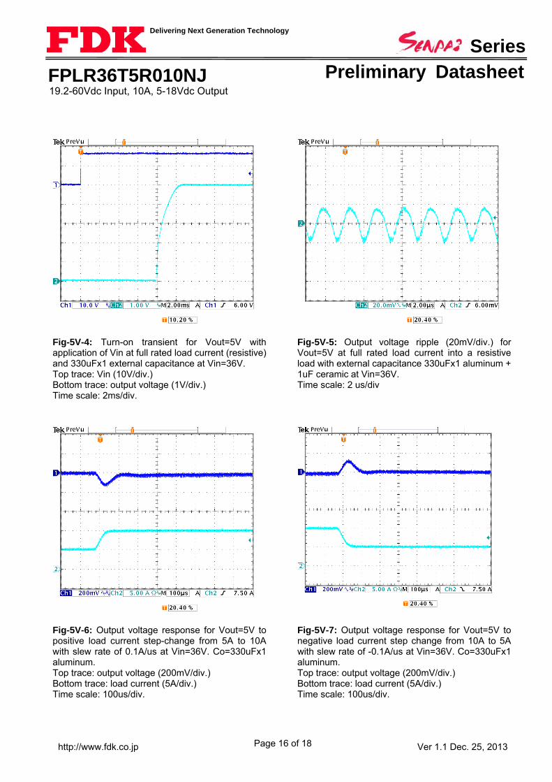
Fig-5V-4: Turn-on transient for Vout=5V with application of Vin at full rated load current (resistive) and 330uFx1 external capacitance at Vin=36V. Top trace: Vin (10V/div.) Bottom trace: output voltage (1V/div.) Time scale: 2ms/div.
Fig-5V-5: Output voltage ripple (20mV/div.) for Vout=5V at full rated load current into a resistive load with external capacitance 330uFx1 aluminum + 1uF ceramic at Vin=36V. Time scale: 2 us/div
Fig-5V-6: Output voltage response for Vout=5V to positive load current step-change from 5A to 10A with slew rate of 0.1A/us at Vin=36V. Co=330uFx1 aluminum. Top trace: output voltage (200mV/div.) Bottom trace: load current (5A/div.) Time scale: 100us/div.
Fig-5V-7: Output voltage response for Vout=5V to negative load current step change from 10A to 5A with slew rate of -0.1A/us at Vin=36V. Co=330uFx1 aluminum. Top trace: output voltage (200mV/div.) Bottom trace: load current (5A/div.) Time scale: 100us/div.

Page 17 of 18
Delivering Next Generation Technology
Series
FPLR36T5R010NJ 19.2-60Vdc Input, 10A, 5-18Vdc Output
http://www.fdk.co.jp Ver 1.1 Dec. 25, 2013
Preliminary Datasheet
Mechanical Drawing
Notes - All dimensions are in millimeters (inches) - Unless otherwise specified, tolerances are +/- 0.25mm - Connector Material: Copper - Connector Finish: Tin over nickel - Converter Weight: 15.4g (0.54oz) - Recommended Through Hole Via: 1.20mm (0.047”) - Recommended Pad Size: 2.00mm (0.079”)

Page 18 of 18
Delivering Next Generation Technology
Series
FPLR36T5R010NJ 19.2-60Vdc Input, 10A, 5-18Vdc Output
http://www.fdk.co.jp Ver 1.1 Dec. 25, 2013
Preliminary Datasheet
Part Numbering Scheme
Product Series
Shape Regulated/
Non Input
Voltage MountingScheme
OutputVoltage
RatedCurrent
ON/OFF Logic
PinShape
FP L R 36 T 5R0 10 N J
Series Name
Large R:
Regulated Typ=36V
Through hole
5V (Programmable:
See page 6) 10A N: Negative J: Right Angle
Notes PATTERN DESIGN: Please prohibit patterns other than 0V shield pattern the pattern drawing under the product considering the interference etc. of the insulation failure and another circuit.
パターン設計: 製品下面へのパターン引き回しは絶縁不良および他回路との干渉等を考慮して0Vシールドパターン以外のパターンは禁止してく
ださい。
NUCLEAR AND MEDICAL APPLICATIONS: FDK Corporation products are not authorized for use as critical components in life support systems, equipment used in hazardous environments, or nuclear control systems without the written consent of FDK Corporation.
核および医療のアプリケーション: FDK製品は生命維持装置、危険な環境に使用される設備、または核制御システムなどにおける重要部
品としては、FDKの承諾書なしでの使用は認可されません。
Operating Conditions: Do not use converters under the following conditions because all these factors deteriorate the converter characteristics or cause failures. 1) Wet or humid locations, 2) corrosive or deoxidizing gas (Hydrogen sulfide, Sulfurous acid, Chloride and ammonia, etc), 3) Volatile or flammable gas, 4) Dusty conditions, 5) Under high pressure or low pressure, 6) location with salt water, oils, chemical liquids or organic solvents, or 7) Strong vibrations or mechanical impact.
使用環境: 本コンバータを以下に示す環境でご使用にならないでください。これらはコンバータの特性を劣化させ、最悪の場合、故障の原
因となります。 1) 水がかかる場所や多湿のために結露するおそれのある場所、2) 腐食性、還元性ガス (硫化水素、亜硫酸、塩素、
アンモニア等) 雰囲気中、3) 揮発性、引火性のあるガス雰囲気、4) 粉塵の多い場所、5) 減圧、または加圧された空気中、6) 塩水、
油、薬液、有機溶剤にさらされる場所、又は 7) 過酷な振動、又は衝撃が加わる場所
HIGH RELIABILITY AND LONG LIFE APPLICATIONS: If FDK Corporation products are used in high reliability or ling life applications, reduce temperature of the converters and determine the condition on your own responsibility after confirming reliability and life time in your actual application.
高信頼性、及び長寿命が要求される装置での使用: 本コンバータを高信頼性、又は張寿命が要求される装置で使用する場合には、本
コンバータの温度低減をするとともに、貴社様の責任において実装置上での信頼性と寿命を確認して使用条件を決定してください。 CLEANSING : Cleansing of this converter is not recommended. When cleansing, determine a cleansing condition on your own responsibility after confirming there is no impact on the characteristics/performance of the converter.
洗浄: 本コンバータの洗浄は推奨いたしません。 洗浄する場合の洗浄条件は、貴社様責任において本コンバータの特性/性能に影響が
無い事を確認して決定してください。
SPECIFICATION CHANGES AND REVISIONS: Specifications are revision-controlled, but are subject to change without notice.
仕様の変更と版数: 仕様は版数によって管理されていますが、予告なしで変更する場合がございます。