department of electronics and communication engineering, manipal institute of technology, manipal,...
TRANSCRIPT

Department of Electronics and Communication Engineering,Manipal Institute of Technology, Manipal, INDIA
Subject Code : ECE – 101/102
BASIC ELECTRONICS
COURSE MATERIALFor
1st & 2nd Semester B.E.(Revised Credit System)
DEPARTMENT OF ELECTRONICS & COMMUNICATION ENGINEERING

Department of Electronics and Communication Engineering,Manipal Institute of Technology, Manipal, INDIA
Bipolar Junction Transistor
• Solid state transistor was invented by a team of scientists at Bell laboratories during 1947-48
• Advantages of solid state transistor over vacuum devices:
– Smaller size, light weight
– No heating elements required
– Lower power consumption and operating voltages
– Low price

Department of Electronics and Communication Engineering,Manipal Institute of Technology, Manipal, INDIA
Different transistor packages

Department of Electronics and Communication Engineering,Manipal Institute of Technology, Manipal, INDIA
Introduction
• Bipolar Junction Transistor (BJT) is a three layer, 2 junction semiconductor device
• It is a sandwich of one type of semiconductor material between two layers of another type
• Two kinds of BJT sandwiches are: NPN and PNP

Department of Electronics and Communication Engineering,Manipal Institute of Technology, Manipal, INDIA
Introduction
• The three layers of BJT are called Emitter, Base and Collector
• Base is narrower compared to the other two layers
• Base is lightly doped, Emitter is heavily doped and Collector is moderately doped
• NPN – Emitter and Collector are made of N-type semiconductors; Base is P-type
• PNP – Emitter and Collector are P-type, Base is N-type
• BJT has two junctions – Emitter-Base (EB) Junction and Collector-Base (CB) Junction

Department of Electronics and Communication Engineering,Manipal Institute of Technology, Manipal, INDIA
Introduction
Note: Arrow direction from P to N (like diode) which indicates the direction of the flow of conventional current
• The device is called “bipolar junction transistor” because current is due to the motion of two types of charge carriers-free electrons & holes
• Transistor symbols:

Department of Electronics and Communication Engineering,Manipal Institute of Technology, Manipal, INDIA
Transistor Operation• Operation of NPN transistor and PNP is similar with roles of
free electrons and holes interchanged
• Depending upon the bias condition (forward or reverse) of each of the two junctions, different regions of operation for the BJT are obtained
Active region- transistor operating as an amplifier and saturation & cutoff region- Switching applications, e.g. in logic circuits
Region

Department of Electronics and Communication Engineering,Manipal Institute of Technology, Manipal, INDIA
Transistor Operation

Department of Electronics and Communication Engineering,Manipal Institute of Technology, Manipal, INDIA
Transistor Operation
• Note the current directions in NPN and PNP transistors• For both varieties:• Collector current has two components:
– One due to injected charge carriers from emitter– Another due to thermally generated minority carriers
Therefore,
C
E
B
IC
IE
IB
NPN
C
E
B
IC
IE
IB
PNP
BCE III
CBOEdcC III

Department of Electronics and Communication Engineering,Manipal Institute of Technology, Manipal, INDIA
Transistor Configurations
• BJT has three terminals
• For two-port applications, one of the BJT terminals needs to be made common between input and output
• Accordingly three configurations exist:
– Common Base (CB) configuration
– Common Emitter (CE) configuration
– Common Collector (CC) configuration
Input Output2-port device

Department of Electronics and Communication EngineeringManipal Institute of Technology, Manipal, INDIA
Transistor Configurations
• Common Base configuration
Base is common between input and output
– Input voltage: VEB Input current: IE
– Output voltage: VCB Output current: IC

• As the currents constituting the collector current are in the same direction, we can write IC as,
• Since ICBO value is very low, we can neglect it compared to IE and IC .
Therefore,
where αdc is the fraction of charge carriers emitted from emitter, that enter into the collector region
• This parameter αdc is called common base DC current gain
• Value of αdc varies from 0.90 to 0.998 and is defined for the majority carriers
• Therefore,
Department of Electronics and Communication Engineering,Manipal Institute of Technology, Manipal, INDIA
CBOEdcC III
Transistor Operation
EdcC II
E
Cdc I
I

Department of Electronics and Communication Engineering,Manipal Institute of Technology, Manipal, INDIA
Transistor Configurations
• CB Input characteristics
– A plot of IE versus VEB for various values of VCB
– It is similar to forward biased diode characteristics
– As VCB is increased, IE increases only slightly

Department of Electronics and Communication Engineering,Manipal Institute of Technology, Manipal, INDIA
Base Width modulation
• As the reverse bias voltage VCB is increased, the depletion
region width at the C-B junction increases. Part of this
depletion region lies in the base layer. So, effective base width
decreases. Hence number of electron-hole combination at the
base decreases. So base current reduces and collector current
increases. Since IE≈IC, emitter current also shoots up early.
• This phenomenon is also called as the Early effect

Department of Electronics and Communication Engineering,Manipal Institute of Technology, Manipal, INDIA
Transistor Configurations
• CB Output characteristics– A plot of IC versus VCB for various values of IE
– Three regions are identified: Active, Cutoff, Saturation

Department of Electronics and Communication Engineering,Manipal Institute of Technology, Manipal, INDIA
Transistor Configurations• In case of Active region
• E-B junction forward biased• C-B junction reverse biased• IC increases with IE
• For given IE, IC is almost constant; increases only slightly with increase in VCB. This is due to base-width modulation
• In the cut off region, E-B and C-B junctions of the transistor are reverse biased
• Collector current is 0A
• In the saturation region, the E-B and C-B junctions of the transistor are forward biased

Department of Electronics and Communication Engineering,Manipal Institute of Technology, Manipal, INDIA
Transistor Configurations
• Common Emitter configuration
Emitter is common between input and output– Input voltage: VBE Input current: IB– Output voltage: VCE Output current: IC

Department of Electronics and Communication Engineering,Manipal Institute of Technology, Manipal, INDIA
Transistor Configurations• CE Input characteristics
Plot of IB versus VBE for various values of VCE . As VCE is increased, IB decreases slightly. This is due to base-width modulation

Department of Electronics and Communication Engineering,Manipal Institute of Technology, Manipal, INDIA
Transistor Configurations• CE Output characteristics
– A plot of IC versus VCE for various values of IB
– Three regions identified: Active, Cut-off, Saturation
VCESat
Department of Electronics and Communication Engineering,Manipal Institute of Technology, Manipal, INDIA
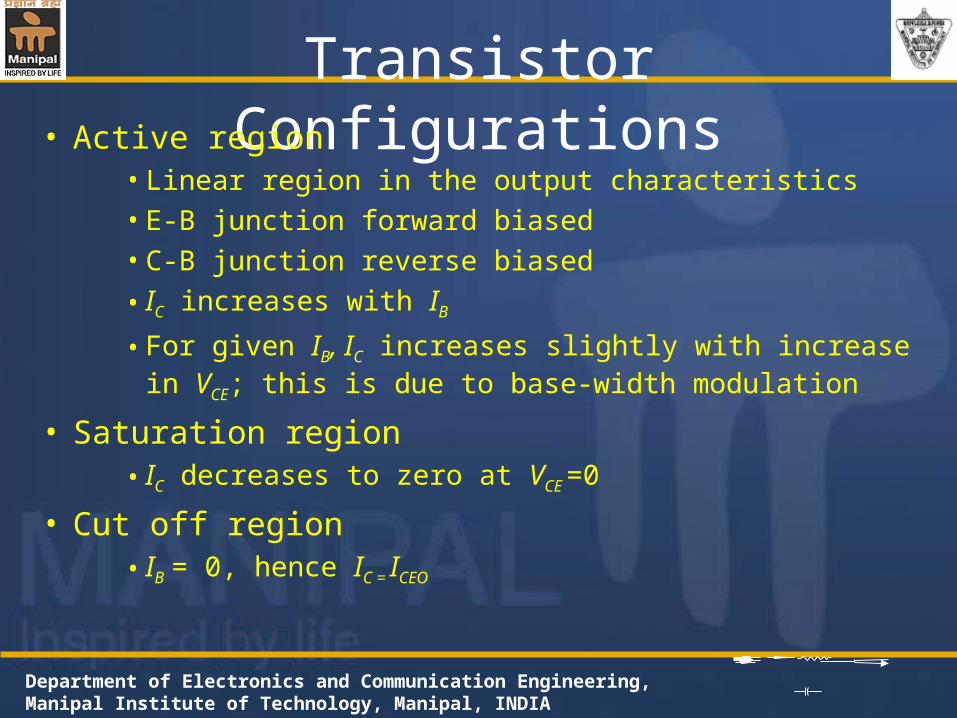
Transistor Configurations• Active region
• Linear region in the output characteristics
• E-B junction forward biased
• C-B junction reverse biased
• IC increases with IB
• For given IB, IC increases slightly with increase in VCE; this is due to base-width modulation
• Saturation region• IC decreases to zero at VCE =0
• Cut off region• IB = 0, hence IC = ICEO

Department of Electronics and Communication Engineering,Manipal Institute of Technology, Manipal, INDIA
Transistor Operation• Parameter βdc is common emitter DC current gain
• Therefore, collector current expression is:
We have,
• Substituting for IE, we getCBOEdcC III
CBOBCdcC IIII CBOBdcCdc III )1(
)1()1( dc
CBOB
dc
dcC
III
CEOBdcC III
where and
Values of αdc and βdc vary from transistor to transistor
)1( dc
dcdc
CBOdcdc
CBOCEO I
II 1
)1(
=
= =
B
Cdc I
I
BdcC II

Department of Electronics and Communication Engineering,Manipal Institute of Technology, Manipal, INDIA
Problems1. A BJT has alpha value as 0.998 and ICBO of 1μA. If emitter current
is 5mA, calculate the collector and base currents.
2. An npn transistor has collector current 4mA and base current 10 μA. Calculate the alpha and beta value of the transistor neglecting the reverse saturation current ICBO.
3. In a transistor, 99% of the carriers injected into the base cross over to the collector region. If collector current is 4mA and ICBO is 6 μA, Calculate IE and IB.
4. A Ge transistor with β = 100 has ICBO = 5μA. If the transistor is connected in common-emitter operation, find the collector current for base current (a) 0 A (b) 40 µA.
5. A Ge transistor has collector current of 51 mA when the base current is 0.4 mA. If β = 125, then what is the value of ICEO?
Department of Electronics and Communication Engineering,Manipal Institute of Technology, Manipal, INDIA
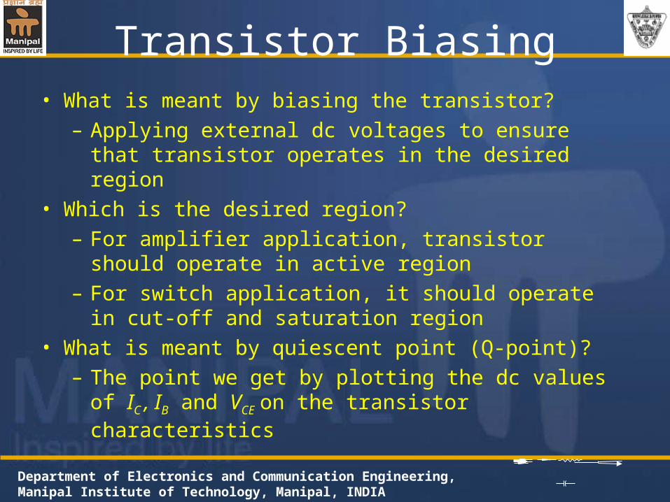
Transistor Biasing• What is meant by biasing the transistor?
– Applying external dc voltages to ensure that transistor operates in the desired region
• Which is the desired region?
– For amplifier application, transistor should operate in active region
– For switch application, it should operate in cut-off and saturation region
• What is meant by quiescent point (Q-point)?
– The point we get by plotting the dc values of IC , IB and VCE on the transistor characteristics

Department of Electronics and Communication Engineering,Manipal Institute of Technology, Manipal, INDIA
Transistor BiasingTransistor characteristics showing Q-point:
• Q-point is in the middle of active region.

Department of Electronics and Communication Engineering,Manipal Institute of Technology, Manipal, INDIA
Transistor Biasing• Types of biasing:
– Fixed bias or base resistor bias– Self bias or voltage divider bias
• Fixed bias:– The value of IB is “fixed” by choosing
proper value for RB
– Equations to be considered are:
B
BECCB R
VVI
CCCCCE RIVV Fixed bias circuit

Department of Electronics and Communication Engineering,Manipal Institute of Technology, Manipal, INDIA
Transistor Biasing• Load Line
We have:
• This is an equation of straight line with points VCC/RC and VCC lying on y-axis and x-axis respectively
• This line is called “Load line” because it depends on resistor RC considered as “Load” and VCC
• Intersection of load line with the transistor characteristic curve is called Q-point or operating point for a particular value of IB, hence giving a common solution
CCCCCE RIVV

Transistor Biasing• If RB is varied, Q-point moves along the load line
• If RB is held constant and RC is varied, then slope of load line varies
• If RB & RC are held constant and VCC is varied, then load line shifts, maintaining same slope
• With reference to the graphs, with everything else held constant
– If RB is increased, transistor goes towards cut-off and if RB is decreased, transistor goes towards saturation
– If RC is increased, transistor goes towards saturation and if RC is decreased, transistor goes towards active region
– If VCC is increased, transistor goes towards active region and if VCC is decreased, transistor goes towards saturation
Department of Electronics and Communication Engineering,Manipal Institute of Technology, Manipal, INDIA

Department of Electronics and Communication Engineering,Manipal Institute of Technology, Manipal, INDIA
Transistor BiasingVariation in load line with circuit parameters RB , RC and VCC

Department of Electronics and Communication Engineering,Manipal Institute of Technology, Manipal, INDIA
Transistor Biasing• Advantages of Fixed bias:
– Simple circuit to analyze and design
– Uses very few circuit components
• Disadvantages of Fixed bias:
– Q-point is unstable i.e. if temperature increases, then β
increases, hence ICQ and VCEQ varies. Effectively Q-point shifts
– If the transistor is replaced with another transistor having
different β value, then also Q-point shifts

Department of Electronics and Communication Engineering,Manipal Institute of Technology, Manipal, INDIA
Problems on Fixed bias1. For a fixed bias circuit using Si transistor, RB = 500 kΩ, RC =
2kΩ, VCC = 15 V, ICBO = 20 µA and β = 70. Find the collector current ICQ and VCEQ at Q-point.
2. A Si transistor is biased for a constant base current. If β = 80, VCEQ = 8 V, RC = 3 kΩ and VCC = 15 V, find ICQ and the value of RB required.
Repeat the problem if the transistor is a germanium device.
3. For a fixed bias circuit, VCC = 12 V and RC = 4 kΩ. The Ge transistor used is characterized by β = 50, ICEO = 0 A and
VCE sat = 0.2 V. Find the value of RB that just results in saturation
4. A fixed bias circuit has VCC = 20 V, RC = 5 kΩ and RB = 300 kΩ. The Si transistor has ICBO = 0 and β = 50. Find ICQ and VCEQ.

Department of Electronics and Communication Engineering,Manipal Institute of Technology, Manipal, INDIA
Transistor Biasing• Voltage divider bias or Self bias
– Resistor RE connected between emitter and ground
– Voltage-divider resistors R1 & R2 replace RB
– Circuit can be analyzed in two methods:
• Exact method (using Thevenin’s theorem)
• Approximation method (neglecting base current)
Self bias circuit

Department of Electronics and Communication Engineering,Manipal Institute of Technology, Manipal, INDIA
Transistor Biasing• Exact method:
– Input side of self-bias circuit (Fig. a) is transformed into Thevenin’s equivalent circuit (Fig. b) where, RTH is the resistance looking into the terminals A & B (Fig. c)
21
2
RR
RVV CC
TH
21
2121 ||
RR
RRRRRTH

Department of Electronics and Communication Engineering,Manipal Institute of Technology, Manipal, INDIA
Transistor Biasing
ETH
BETHB RR
VVI
)1(
E
BETHB R
VVI
E
BETHBC R
VVII
Equations to be considered:
Since β >> 1 and (β+1)RE >> RTH
Since IC is almost independent of β, Q-point is stable
• Self-bias circuit redrawn with input side replaced by Thevenin’s equivalent :
EECCCCCE RIRIVV

Transistor Biasing
• Advantages of Self bias:
– The collector current and hence the Q-point is independent of variation in temperature and replacement of transistor
• Disadvantages of Self bias:
– More circuit components are required
– Analysis and design are complex
Department of Electronics and Communication Engineering,Manipal Institute of Technology, Manipal, INDIA

Department of Electronics and Communication Engineering,Manipal Institute of Technology, Manipal, INDIA
Problems on Self bias1. For a self bias circuit, the transistor is a Si device, RE = 200 Ω,
R1 = 10R2 = 10 kΩ, RC = 2 kΩ, β = 100 and VCC = 15 V. Determine the values of ICQ and VCEQ.
2. Suppose if the transistor used in problem 1 failed and was replaced with a new transistor with β = 75, is the new transistor still biased for active region operation?
3. A self bias circuit uses Silicon transistor with RC = 3.3K Ω,
RE = 1KΩ, R1 = 39K Ω, R2 = 8.2K Ω, β = 120 and VCC = 18 V. Determine the values of IB , ICQ and VCEQ.

Department of Electronics and Communication Engineering,Manipal Institute of Technology, Manipal, INDIA
Transistor Amplifier• Amplifier
– Circuit which increases the magnitude of the input signal applied
– BJT basically amplifies current: Collector current equals beta times Base current
– By suitably designing the transistor circuit, we can get voltage amplification and power amplification
– For faithful amplification (with no distortion), BJT should operate in Active region throughout the input cycle
– This is achieved by proper use of biasing circuit– Biasing circuit fixes the operating point in the middle of
active region

Department of Electronics and Communication Engineering,Manipal Institute of Technology, Manipal, INDIA
Transistor Amplifier• As vin varies, iin varies, thus base current iB varies• This variation in base current is amplified beta times to get variation in collector current iC
• Output voltage vout is VCC – iC RC
• If vin increases, there is proportional decrease in vout
• Similarly if vin decreases, vout increases proportionally• Thus output voltage of CE amplifier is 180o out of phase with input voltage
CE amplifier circuit with fixed bias

Department of Electronics and Communication Engineering,Manipal Institute of Technology, Manipal, INDIA
Transistor Amplifier
• Voltage gain or voltage amplification factor is vout /vin
which is dependent on β, RC and other physical parameters of the transistor
• Figure shows input and output waveforms for the amplifier circuit shown previously
• Note the dc shift in the output voltage waveform. i.e., when vin = 0, vout = VCEQ

Department of Electronics and Communication Engineering,Manipal Institute of Technology, Manipal, INDIA
Transistor Amplifier
• Gain of the amplifier is usually expressed in decibels
• (AV)dB = 20 log10 | AV |
• Usually a gain of 100 (i.e. 40 dB) can be obtained using single transistor. For higher gain requirement, two or more amplifier stages are to be cascaded
• Overall gain is product of individual gains, but when expressed in dB, overall gain is sum of individual gains (in dB)
VNVVV AAAA ........ 21
dBVNdBVdBVdBV AAAA )(.......)()()( 21

Department of Electronics and Communication Engineering,Manipal Institute of Technology, Manipal, INDIA
Transistor Amplifier• RC Coupled Amplifier
CE amplifier employing self bias

Department of Electronics and Communication Engineering,Manipal Institute of Technology, Manipal, INDIA
Transistor Amplifier• Additional components used are CC and CE
– CC is called coupling capacitor – used to prevent dc component from entering or leaving amplifier stage
– CE is called emitter bypass capacitor – used to bypass the ac emitter current – preventing it from flowing through RE
– If ac emitter current is allowed to pass through RE, then vBE reduces and hence output voltage reduces
• Frequency response of amplifier– It is important to know the behavior of the amplifier at different
frequencies – Gain is NOT constant at all frequencies – depends on various
factors– Frequency response is a plot of gain versus frequency

Department of Electronics and Communication Engineering,Manipal Institute of Technology, Manipal, INDIA
Transistor Amplifier
• Figure shows frequency response plot
• At lower and higher frequencies, gain is less
• Gain attains constant
value at mid frequencies
• Bandwidth of amplifier is range of frequencies over which gain is not less than
3 dB of maximum gain

Department of Electronics and Communication Engineering,Manipal Institute of Technology, Manipal, INDIA
Transistor Amplifier• Analysis of frequency response curve
– At very low frequencies, reactance of coupling capacitors is high, hence there is loss of signal voltage across capacitors, resulting in reduced gain
– Also at low frequencies, emitter bypass capacitor does not fully bypass the ac emitter current, hence ac voltage drop develops across RE, resulting in reduced gain
– At very high frequencies, shunt capacitances due to wiring and inter-layer junction capacitances will be prominent, hence resulting in signal loss
– At mid frequencies, gain is maximum and constant

Transistor Amplifier• Advantages
• Cost is low
• Offers high fidelity in audio frequency range (20 - 20KHz)
• Circuit is quite compact
• Disadvantages• Tends to be noisier with age
• Gain is less
Department of Electronics and Communication Engineering,Manipal Institute of Technology, Manipal, INDIA

Department of Electronics and Communication Engineering,Manipal Institute of Technology, Manipal, INDIA
Problems on Amplifiers1. A three-stage amplifier circuit has first stage gain of 45 dB,
second stage gain of 50 dB and third stage gain of –5 dB. What is the overall gain? If input to the first stage is 0.1mV, what is the output of final stage?
2. An amplifier has maximum gain of 200 and bandwidth of 500 kHz. If lower cutoff frequency is 50 Hz, what is the upper cutoff frequency and gain at this frequency?
3. The voltage amplifier has a voltage gain = 200 at the cut off frequencies. Find the maximum voltage gain?

Department of Electronics and Communication Engineering,Manipal Institute of Technology, Manipal, INDIA
End of Module 6