department of electronics - elec%4705%lec%15%tjs/opticalsystemsandfab.pdf · 2019-04-05 · david...
TRANSCRIPT

Elec%4705%Lec%15%
Op.cal%Systems%and%integrated%
Op.cs%

What’s%wrong%with%electrical%
transmission?%• The%maximum%rate%of%informa.on%transfer%is%
limited%by%the%number%of%bits%per%second%
that%can%be%transmiEed.%
• As%the%bit%rate%increases,%the%individual%pulse%represen.ng%a%bit%must%be%turned%on%
and%off%faster.%%
• The%nonKzero%resistance%of%the%metal%and%
capacitance%in%a%metal%cable%limit%this%
transi.on%.me%to%t%>%10%nanoseconds%
(10x10K9%seconds).%

What’s%wrong%with%electrical%
transmission?%
• Maximum%bit%rate%of%100’s%of%megabits/
second%
• Pulse%are%distorted%as%they%travel.%• Short%pulses%merge%causing%loss%of%
informa.on.%
• Introduc.on%of%noise.%

BeEer%Electrical?%
• Geometry%is%used%to%
create%good%electrical%
lines.%
• Coaxial%lines%are%about%as%good%as%you%
can%get.%
• %On%boards%and%chips%we%use%a%variety%of%
stripKlines%with%
ground%planes.%

Transmission%Lines%
• Approxima.on%of%par.al%differen.al%
equa.on.%
• Include%coupling%capacitances%and%inductors.%%• RLC%is%essen.ally%lowKpass%causing%the%pulses%to%broaden.%

Electrical%Effects%• High%frequencies%couple%through%capacitors.%
• Cause%pulse%edges%to%be%coupled%to%adjacent%lines.%%
• Makes%a%mess%of%the%signals.%
• Electrical%Magne.c%Interference%(EMI).%

Electrons%vs%Photons%

Op.cal%Communica.ons%System%
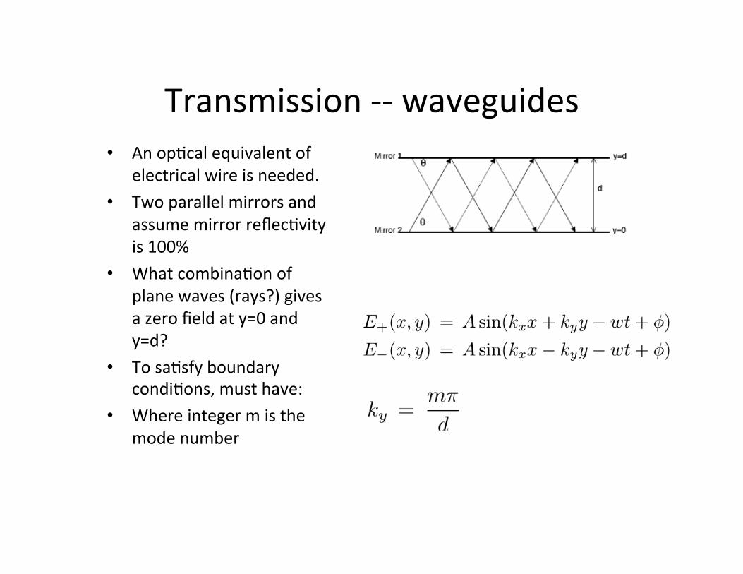
Transmission%KK%waveguides%• An%op.cal%equivalent%of%
electrical%wire%is%needed.%
• Two%parallel%mirrors%and%assume%mirror%reflec.vity%is%100%%
• What%combina.on%of%plane%waves%(rays?)%gives%a%zero%field%at%y=0%and%y=d?%
• To%sa.sfy%boundary%condi.ons,%must%have:%
• Where%integer%m%is%the%mode%number%

Transmission%KK%waveguides%• Summing%the%two%waves%together%gives%
• The%mode%propaga.on%constant%is%defined%as:%
• Light%can%only%propagate%in%the%form%of%these%modes%inside%a%waveguide%
• βm%can%only%have%discrete%values.%
• The%mode%Effec.ve%Index%is%given%by%%• Speed%of%light%depends%on%the%mode%as%%
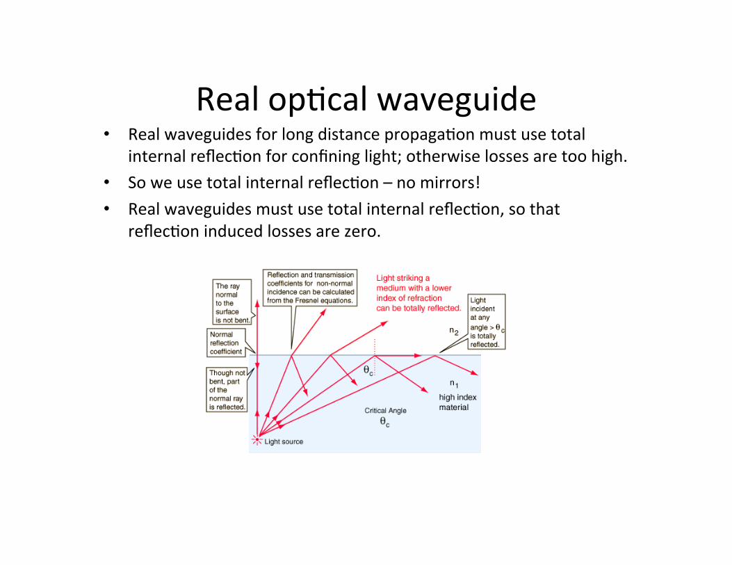
Real%op.cal%waveguide%• Real%waveguides%for%long%distance%propaga.on%must%use%total%
internal%reflec.on%for%confining%light;%otherwise%losses%are%too%high.%
• So%we%use%total%internal%reflec.on%–%no%mirrors!%
• Real%waveguides%must%use%total%internal%reflec.on,%so%that%reflec.on%induced%losses%are%zero.%

Real%op.cal%waveguide%• Op.cal%waveguide%has%a%core%and%cladding%with%
different%n’s%• Choose%nclad%<%ncore%and%core%diameter%d%small%enough%
that%only%the%fundamental%E_%mode%is%supported.%• We%need%ncore%>%nclad.%• Φm%must%be%less%than%the%cri.cal%angle%for%total%
internal%reflec.on,%hence%the%number%of%modes%is%restricted.%
• It%is%possible%to%make%single%mode%waveguides,%for%small%index%difference%and/or%small%core%thicknesses.%
• Guided%light%spills%over%into%evanescent%tails%in%the%cladding%regions.%
• The%effec.ve%index%Neff%always%lies%somewhere%between%the%index%of%the%core%and%the%index%of%the%cladding.%

Op.cal%fiber%• Op.cal%fibre%is%a%glass%waveguide%
with%a%cylindrical%crossKsec.on%– Mul.mode%K%Cheap%and%used%for%short%
distances.%Mode%dispersion.%
– Single%mode%K%More%expensive%and%carefully%designed%for%low%dispersion,%low%loss%and%long%distances.%

Op.cal%fiber%KK%aEenua.on%• λ%=%1300%nm%wavelength%of%minimum%index%dispersion%(the%varia.on%of%
index%n%with%wavelengthK%an%intrinsic%property%of%glass)%• λ=%1550%nm%wavelength%of%minimum%loss%(due%to%impuri.es%and%molecular%
vibra.on%absorp.on%by%OKH,%SiKH).%
• A%number%of%regions%are%used%extensively.%
• Enormous%bandwith%in%each%region%(THz).%
• How%to%use%it?%%
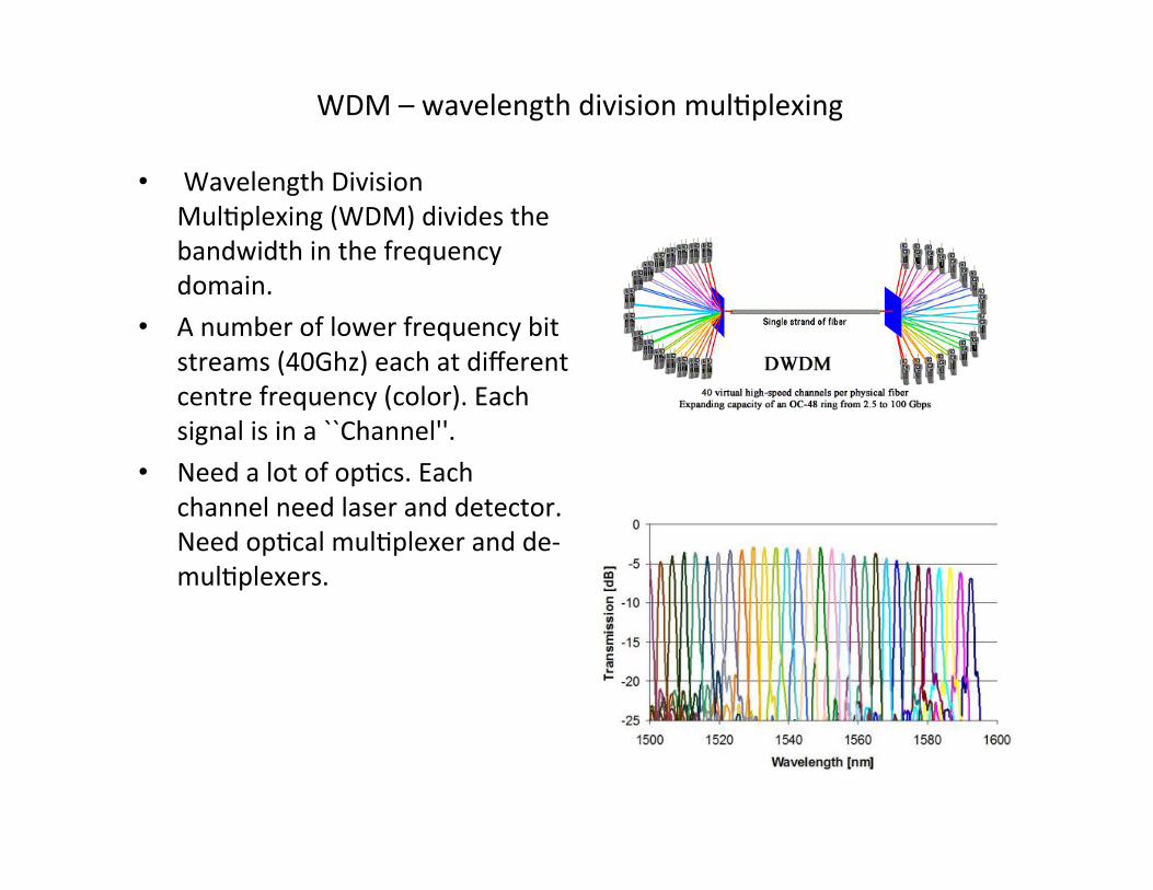
WDM%–%wavelength%division%mul.plexing%
• %Wavelength%Division%Mul.plexing%(WDM)%divides%the%bandwidth%in%the%frequency%domain.%
• A%number%of%lower%frequency%bit%streams%(40Ghz)%each%at%different%centre%frequency%(color).%Each%signal%is%in%a%``Channel''.%
• Need%a%lot%of%op.cs.%Each%channel%need%laser%and%detector.%Need%op.cal%mul.plexer%and%deKmul.plexers.%

TDM%–%TimeKdomain%division%mul.plexing%
• %Time%division%mul.plexing%(TDM)%divides%the%bandwidth%in%the%.me%domain.%
• A%number%of%very%high%frequency%bit%streams%(very%short%pulses).%Are%interwoven%in%the%.me%domain.%%
• Need%a%lot%of%electronics%and%a%very%fast%op.cal%modulator%and%detector.%%

More%complicated%methods%
• %Can%get%clever%and%mix%TDM%and%WDM%(OFDM)%
• Can%also%code%the%bits%on%the%op.cal%phase.%
• 40GHz%bit%stream%with%4%levels%using%phase%at%0,%π/2,%π%,%3/2π%can%be%done%with%10GHz%pulse%stream.%

Structured%FIBER%
• %Fancy%nanostructured%fiber%has%been%proposed%for%sensors%and%other%applica.ons.%%
• %Photonic%crystal%fibers%use%a%periodic%structure%to%confine%the%light%

FIBER%SENSORS%
• %Fibers%are%very%sensi.ve%to%the%refrac.ve%index%of%both%core%and%cladding.%
• Anything%that%changes%this%(Temperature,%stress,%chemistry,%etc)%can%be%sensed%by%looking%at%the%loss,%aEenua.on%and%phase%shirs%that%occur.%
• Many%sensors%based%on%a%lot%of%different%structures.%
• %Work%at%Carleton%uses%a%.lted%gra.ng%to%excite%a%gold%film%deposited%on%the%fiber.%%
• Sense%any%disturbance%of%the%gold%film.%
• Uses%include%DNA%detec.on,%Cell%process%inves.ga.on,%chemical%composi.on,%etc.%

Silicon Photonic Integration
Columbia University 20
MIT, 2008
IBM, 2007
Cornell, 2005
Luxtera, 2005 UCSB, 2006

On%chip%waveguides%
1. Typically%a%ridge%wave%guide%2. Oren%built%in%Silicon%on%Insulator%
(SOI)%3. Can%be%single%or%mul.Kmode%4. Many%devices%can%be%fabricated%
1. Joiners/SpliEers%2. Couplers%3. Resonators%4. Lasers/Amplifiers%(PN%diode%
with%ridge%wave%guide%5. Filters%6. Mul.Kplexers%

Vision of Photonic Integration
Columbia University 22

Hybrid Opto-electronic Chip
Columbia University
P G
P G
P G
P G
P G
P G
P G
P G
P G
Processing Core (on processor plane) Gateway to Photonic chip (between processor & photonic planes)
Thin Electrical Control Network (~1% BW, small messages)
Photonic Deflection Switch
DARPA phase I ICON project

Key Building Blocks
5cm SOI nanowire 1.28Tb/s (32 λ x 40Gb/s)
LOW%LOSS%BROADBAND%NANOKWIRES%
HIGHKSPEED%MODULATOR%
Cornell
BROADBAND%MULTIKλ%ROUTER%SWITCH%
HIGHKSPEED%RECEIVER%
IBM/Columbia
Cornell/ Columbia
IBM
IBM

Microring Resonators • Valuable building blocks for SOI-based systems
! Passive operations ! Filtering and multiplexing
! Active functions ! Electro-optic, thermo-optic, all-optical switching/modulation
Q. Xu et al., Opt. Express, Jan 2007 B. E. Little et al., PTL, Apr 1998 P. Dong et al., CLEO, May 2007
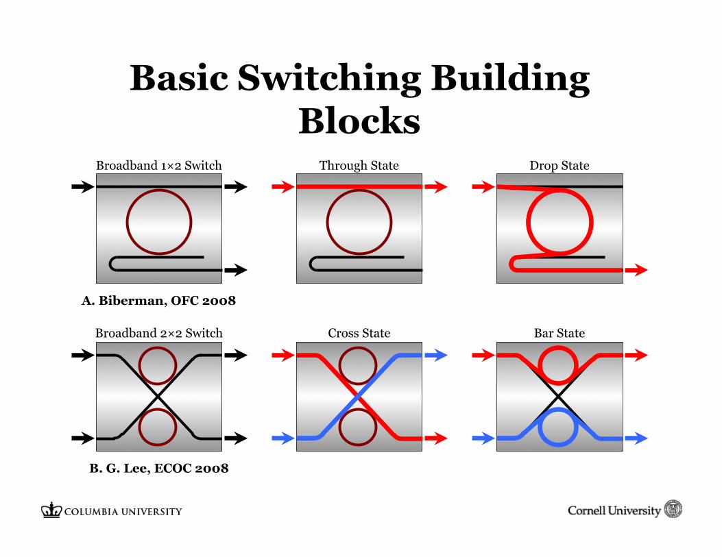
Basic Switching Building Blocks
Broadband 1×2 Switch
A. Biberman, OFC 2008
Broadband 2×2 Switch
B. G. Lee, ECOC 2008
Through State Drop State
Cross State Bar State

Switch Operation
Columbia University 27
in0
in1
out0
out1
λ
Tra
nsm
issi
on
bar
cross

Non-Blocking 4×4 Switch Design
Columbia University 28
• Original switch: internally blocking
• New design: – Strictly non-blocking* – Same number of rings – Negligible additional loss – Larger area
* U-turns not allowed

Basic Integrated Circuit Processing
ELEC 3908, Physical Electronics, Lecture 4

David J. Walkey ELEC 3908, Physical Electronics: Basic IC Processing (4) Page 3
Ingot Growth• First step in production of an
integrated circuit is growth of a large piece of almost perfectly crystalline semiconductingmaterial called an ingot (boule)
• Small seed crystal is suspended in molten material then pulled (1m/hr) and rotated (1/2 rps) to form the ingot
• Result is an ingot approx. 1m long and anywhere from 75 to 300 mm in diameter
• Dopant is almost always added to the molten material

David J. Walkey ELEC 3908, Physical Electronics: Basic IC Processing (4) Page 4
Ingot Growth
David J. Walkey ELEC 3908, Physical Electronics: Basic IC Processing (4) Page 5
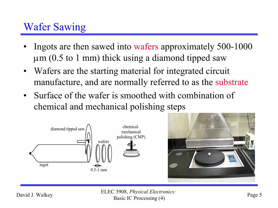
Wafer Sawing
• Ingots are then sawed into wafers approximately 500-1000 μm (0.5 to 1 mm) thick using a diamond tipped saw
• Wafers are the starting material for integrated circuit manufacture, and are normally referred to as the substrate
• Surface of the wafer is smoothed with combination of chemical and mechanical polishing steps

David J. Walkey ELEC 3908, Physical Electronics: Basic IC Processing (4) Page 6
Photolithography
• Lithography refers to the transfer of an image onto paper using a plate and ink-soluble grease
• Photolithography is the transfer of an image using photographic techniques
• Photolithography transfers designer generated information (device placement and interconnections) to an actual ICstructure using masks which contain the geometrical information
• The process of photolithography is repeated many times in manufacture of an IC to build up device structures and interconnections

David J. Walkey ELEC 3908, Physical Electronics: Basic IC Processing (4) Page 7
Photolithography - Application of Photoresist• First step in photolithography is
to coat the surface with approx 1 μm of photoresist (PR)
• PR will be the medium whereby the required image is transferred to the surface
• PR is often applied to the center of the wafer, which is then spun to force the PR over the entire surface
• Note that the scale of these diagrams is not correct - the PR is approx. 1 μm thick while the wafer is 1000 μm thick.

David J. Walkey ELEC 3908, Physical Electronics: Basic IC Processing (4) Page 8
Photolithography - Exposure• The PR is then exposed to UV
(ultraviolet) radiation through a mask
• The masks generated from information about device placement and connection
• The UV radiation causes a chemical change in the PR
• The transfer of information from the mask to the surface occurs through the UV-induced chemical change - only occurs where the mask is transparent
wafer
mask mask
UV radiation

David J. Walkey ELEC 3908, Physical Electronics: Basic IC Processing (4) Page 9
Photolithography - Development• The PR is then developed using
a chemical developer• Two possibilities:
– A negative PR is hardened against the developer by the UV radiation, and hence remains on the surface where UV shone through the mask
– A positive PR is the opposite, it is removed where the UV shone through the mask
• Assume a negative PR for this example, so the PR on the sides will be weakened and removed by the developer

David J. Walkey ELEC 3908, Physical Electronics: Basic IC Processing (4) Page 15
Example Simple Mask Set
• Shown below is a highly simplified layout for a two transistor digital gate, and the masks which would be required based on its layout (see MOSFET)
• Not in notes, just shown as an example of how masks are derived from a user-generated layout
layout (4 layers) layer 1 mask layer 2 mask layer 3 mask layer 4 mask

David J. Walkey ELEC 3908, Physical Electronics: Basic IC Processing (4) Page 16
Etching - Dry and Wet Processes• Etching is the selective removal
of material from the chip surface
• In dry etching, ions of a neutral material are accelerated toward the surface and cause ejection of atoms of all materials
• In wet etching, a chemical etchant is used to remove material via a chemical reaction

David J. Walkey ELEC 3908, Physical Electronics: Basic IC Processing (4) Page 18
Thermal Oxidation - Oxidation Furnace• One of the simplest steps in IC processing is thermal oxidation, the
growth of a layer of silicon dioxide (SiO2) on the substrate surface• Requires only substrate heating to 900-1200 °C in a dry (O2) or wet
(H20 steam) ambient using an oxidation furnace• Silicon oxidizes quite readily - one reason why Si is so widely used
David J. Walkey ELEC 3908, Physical Electronics: Basic IC Processing (4) Page 24
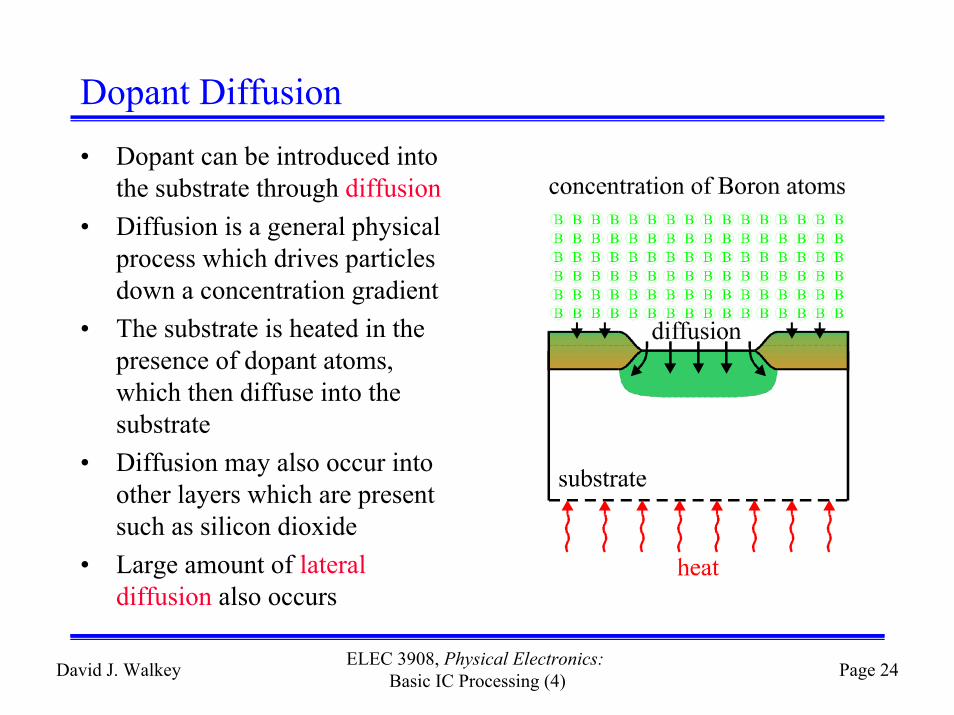
Dopant Diffusion• Dopant can be introduced into
the substrate through diffusion• Diffusion is a general physical
process which drives particles down a concentration gradient
• The substrate is heated in the presence of dopant atoms, which then diffuse into the substrate
• Diffusion may also occur into other layers which are present such as silicon dioxide
• Large amount of lateral diffusion also occurs

David J. Walkey ELEC 3908, Physical Electronics: Basic IC Processing (4) Page 25
Ion Implantation• In ion implantation, dopant
atoms are accelerated toward the substrate surface and enter due to their kinetic energy
• This is the preferred technique for introduction of dopantatoms since the amount of lateral diffusion is much lower

David J. Walkey ELEC 3908, Physical Electronics: Basic IC Processing (4) Page 28
Deposition
• Layers of materials such as metal (and in some cases silicon dioxide) may need to be formed on the surface
• General procedure of forming a layer of material on the surface is termed deposition
• Two types can be identified, physical and chemical– In physical deposition, a piece (target) of the material to be
deposited is bombarded with ions, ejecting atoms of material which then adhere to the substrate surface
– Chemical deposition uses an ongoing chemical reaction to form the desired material as a precipitate on the substrate surface
• A specialized form of deposition is epitaxy, the formation of a layer of crystalline semiconductor material

David J. Walkey ELEC 3908, Physical Electronics: Basic IC Processing (4) Page 29
Sputtering System

David J. Walkey ELEC 3908, Physical Electronics: Basic IC Processing (4) Page 31
Final Fabricated Wafer

David J. Walkey ELEC 3908, Physical Electronics: MOSFET Structure and Processing (20) Page 9
Basic MOSFET Structure - Source and Drain• The source and drain of the
MOSFET are two regions with high doping of opposite type to the substrate immediately adjacent to the edges of the gate
• The source and drain regions are normally contacted with metal, separated from the gate and substrate by a dielectric isolation layer

David J. Walkey ELEC 3908, Physical Electronics: MOSFET Structure and Processing (20) Page 12
MOSFET Fabrication - Active Region Masking• Using a mask, silicon nitride is
patterned to remain in the areas which will form the active region of the MOSFET
• A pad oxide is grown on the surface before deposition of the nitride to protect the silicon surface from damage induced by the different bonding structure of the nitride

David J. Walkey ELEC 3908, Physical Electronics: MOSFET Structure and Processing (20) Page 13
MOSFET Fabrication - Field Oxide Formation• Using wet oxidation (since the
quality is not critical and a thick layer is required), the field oxide is grown on the wafer surface outside the active areas

David J. Walkey ELEC 3908, Physical Electronics: MOSFET Structure and Processing (20) Page 14
MOSFET Fabrication - Device Well Structure• After the nitride and pad oxide
are stripped, the active area is surrounded by field oxide and therefore lies inside a “well” in the field oxide
• This is the origin of the term device well to refer to the active area of the MOSFET
• The active area mask is sometimes called the device well mask

David J. Walkey ELEC 3908, Physical Electronics: MOSFET Structure and Processing (20) Page 16
MOSFET Fabrication - Gate Connection• The gate within the MOSFET
area as well as all other polysilicon lines are formed simulataneously
• The gate is connected by running the polysilicon up onto the field oxide and to another point or eventually to a connection to metal

David J. Walkey ELEC 3908, Physical Electronics: MOSFET Structure and Processing (20) Page 17
MOSFET Fabrication - Source/Drain Implantation• The source and drain are then
implanted with the gate in place• This process is called self
aligned, since the source and drain do not need to be optically aligned with the gate
• Some lateral diffusion occurs which makes the actually distance between the source and drain less than the length of the gate material

David J. Walkey ELEC 3908, Physical Electronics: MOSFET Structure and Processing (20) Page 19
MOSFET Fabrication - Metallization• Metal is deposited over the
back side of the wafer to form the backside substrate contact
• Metal is also deposited on the surface and patterned using the metal mask

David J. Walkey ELEC 3908, Physical Electronics: MOSFET Structure and Processing (20) Page 20
MOSFET Fabrication - Metallization• Metallization surrounds the
contact cut area, which is normally constrained to be within the source drain region
• Metal to polysilicon connection would have been made elsewhere (on top of field oxide)

MicroFabrication Facility
(CUMFF) Faculty of Engineering and Design,
Department of Electronics
CUMFF Class 100 Cleanroom area
The Carleton University MicroFabrication Facility is a class 100 to 10,000 - 3200 square foot cleanroom facility used for manufacturing silicon integrated circuits and other device materials in support of research on: process technology, device physics/modeling, innovative circuit techniques, photonics, biomedical devices, renewable energy (solar cells) and micro-electromechanical systems (MEMS).
While the facility’s primary objective is to support Carleton graduate student research and fabricate annual undergraduate 4th year projects, external academic and industrial users are also welcome to access the lab and equipment for research work or small-volume production runs.
The CUMFF facility has hosted several start-up companies and our experienced/industry trained lab staff have completed numerous contract projects.
A notable strength of the CUMFF is in MOS processing; MOS gate dielectrics can be produced with contamination at industry acceptable levels. To illustrate this capability, every year the CUMFF lab is used in a quasi-production mode to fabricate student submitted designs on a multi-project chip from layout to completed chip. The project uses 5µm LOCOS-isolated polysilicon gate nMOS technology, and more recently cMOS technology on SOI material. These designs typically contain 50 to 100 transistors. Working chips are returned for testing within approximately three weeks of submission of CAD files, and wafer-level probing usually indicates yields of over 80% for the circuits.
Facility Layout The Microfabrication Facility is located on the 4th floor of the Minto Center for Advanced Engineering building and has a total clean room floor area of approximately 3200 ft2. The lab contains four distinct working areas for photolithography, photomask preparation, furnace operations, and high vacuum processes, each separated by a service bay. A separate air conditioning system maintains the facility temperature at 20°C with 40% relative humidity throughout the year. Class 100 air quality is
maintained in the photolithography and photomask production areas (approximately 80 m2 total), Class 1,000 in the vacuum system area and class 10,000 in the oxidation/diffusion area.
Photomask Generation
Photomasks are generated in-house from CIF files using a David Mann 3000 pattern generator system, and a Jade step-and-repeat camera providing 10X reduction. Both the pattern generator and the step-and- repeat camera use high resolution silver halide emulsion photographic plates. The pattern generator can resolve 4 µm features with 4 µm spacing. The minimum feature size obtainable with the step-and-repeat camera is approximately 1.5 µm, limited primarily by the grain size of the photographic plates. Chrome photomasks are available through external vendors.
Photolithography Photolithography is carried out using a Karl-Suss MA6 UV mask aligner, which can accept substrates ranging from small fragments to 100 mm diameter wafers. Feature sizes down to 0.8 µm have been printed using chrome masks. A HMDS vapor oven, photoresist spinners, bake ovens, hotplates and developing benches are used for the photoresist processing.

Oxidation/Diffusion
An eight-stack Bruce Model BDF-8 furnace bank is available for thermal processing up to 1200 C on wafers up to 100 mm in diameter. Tubes for oxidation, implant annealing and drive-in, phosphorus predeposition and hydrogen metal sinter are operational. Gettering with HCl gas is used before all oxidation cycles to control Na+ ionic contamination. With this precaution it is possible to produce gate oxides showing effectively no flatband shift in bias-temperature stress tests.
LPCVD/PECVD A four-stack Bruce furnace bank is used for Low Pressure Chemical Vapor Deposition. Depositions include: LPCVD Oxides (doped and undoped), BPSG, Amorphous Silicon and PolySilicon, and Silicon Nitride. A Trion Orion III PECVD system used for PECVD Silicon Nitride, Silicon dioxide and hydrogenated silicon films on up to 8” wafers.
Cleaning and Wet Etching Several wet benches with exhaust and cascade rinsers are available throughout the lab for wet chemical processing and cleaning.. Ultrapure18 Mega ohm DI (De-ionized) water is produced onsite, stored in a 200 gallon tank and continuously re-circulated throughout the lab to maintain purity. Clean DI water is essential for the production of semiconductor devices.
Plasma Etching
Several dry etch systems are available in the Microfabrication Lab. A MRC RIE 61 reactive ion etcher is used for oxide etching, including sidewall spacer formation. Vertical-walled optical waveguides 10 µm high have been etched in deposited SiO2 layers to form optical waveguides. Other plasma etch systems include a Technics Planar Etch II ,a March RIE etcher and 2 microwave plasma etchers for resist stripping.
Metallization and Thin Films
Several multi-purpose metal deposition systems are available: A loadlocked inline Semicore sputtering system with sputter etch capability, two ebeam/thermal evaporator systems, and a Varian M2000 single chamber RF/DC sputter system. A number of different materials can be deposited including Al, Ti, Au, Ag, SiO2, Cr, Pt etc.
Access to Atomic Layer Deposition processing (ALD), is available through the newly opened Facility for Nanostructures, Surfaces, and Sensor Interfaces (FANSSI) facility on the 5th floor of the Minto Building. This new Chemistry/Electronics shared facility includes a wetlab and a class 10,000 cleanroom lab. The equipment set includes a Picosun Atomic Layer deposition system, a Angstrom Engineering Thermal Evaporation system housed inside a Mbraun high purity glovebox, and a Trion PECVD system.
Process Monitoring
Optical microscopes are available throughout the lab for optical inspections, taking photographs and making linewidths measurements if necessary. For film thickness measurements we have ellipsometers, as well as contact and optical profilometers.. A complete 1 MHz CV test station consisting of a hot chuck with a HP4280 CV meter is available to test gate dielectric quality. A Jeol JSM840 Scanning electron microscope is available for SEM imaging.
Dicing/wirebonding/testing Wafer dicing, wirebonding and testing equipment is also available for non-production type projects. CUMFF Contacts: Dr. Garry Tarr, CUMFF Faculty Coordinator. 613-520-5758, [email protected] Rob Vandusen, CUMFF Facility Manager. 613-520-5761, [email protected] www.doe.carleton.ca/content/microfabrication-facility