department of technology and built environment - diva portal423203/fulltext01.pdf · department of...
TRANSCRIPT

Department of Technology and Built
Environment
Modeling of a Tunable Thin Film Bulk Acoustic Resonator and
Bandpass Filter design based on Ferroelectric Film
Master’s Thesis in Electronics/Telecommunication
Usman Javaid
June, 2011
Supervisor: Prof. Spartak Gevorgian
Terahertz and Millimeter Wave Laboratory, Department of Microtechnology and Nanosciences-
MC2,
Chalmers University of Technology, SE-41296 Gothenburg, Sweden
Examiner: Dr. Jose Chilo
Department of Technology and Built Environment,
University of Gavle, Sweden

I
To
My Parents

II
PREFACE This thesis is a result of my research at Tera Hertz and millimeter wave laboratory of Chalmers University of Technology, Sweden to fulfill the requirement for the Master degree in Electronics/Telecommunication Engineering at University of Gavle, Sweden. Professor Spartak Gevorgian, Professor in Chalmers University of Technology and senior specialist at Ericsson, supervised me and guide me during the whole period of research. The thesis work is examined by Dr. Jose Chilo at University of Gavle. The main purpose of the thesis is to design a tunable bandpass filter. A single tunable film bulk acoustic resonator (TFBAR) is the building block to design the bandpass filter. The simulations of single FBAR resonator are based on measurements, taken by John Berge, the PhD Student at Chalmers University of technology. Advance Design System (ADS) by Agilent technology is used for simulations. The measurement data is reproduced in ADS simulations by using MASON and Butterworth Van Dyke model and by using this data a tunable bandpass filter for 5GHz applications is designed.

III
Abstract
Filters having smallest size, high power handling capability, high Q factor, operating frequency up to
several gigahertz’s (GHz) and low cost are the demand of the market to use in front end wireless/radio
communication systems. In this regard several filter technologies have been introduced and utilized
commercially. The increasing demand of such type of filters has opened a new challenge for filter
designers.
The purpose of this thesis is to design of a Tunable Bandpass Filter based on Barium Strontium Titanate
(BSTO) Ferroelectric Film. A single Film bulk acoustic resonator (FBAR) is measured. MASON and
Butterworth Van-Dyke (BVD) model are studied and implemented to reproduce the measurements.
Simulations are performed by using the Advance Design System (ADS) by Agilent technologies.
Simulations and measured data are used to exactly extract the physical and electrical parameters of a
single FBAR.
FBAR filter topologies are being studied and implemented. Ladder filter topology is selected to design
the bandpass filter. The extracted physical and electrical parameters are used to investigate the
performance of the filter. The area and the top electrode thickness of the series and shunt resonators
are optimized to achieve the bandpass response with maximum out of band rejection, minimum
insertion loss and sharper roll off near the pass band.
A 3rd order T-type bandpass filter for 5GHz applications is designed. The insertion loss of -2.925 dB is
achieved. The filter exhibits the 3dB bandwidth of 176 MHz and out of band rejection of -10 dB. DC bias
of 0-25 V is used to analyze the tuning behavior of the filter. The electromagnetic co-simulation is also
done in momentum to analyze the parasitic effects between the resonators. The results show the good
agreement between the schematic and momentum simulation.
Layout and masks are also designed on a 10*10 mm wafer that will be used later to fabricate the filter
and further investigations.
Keywords: BSTO, FBAR, BVD, Ferroelectric Bandpass filter

IV
Acknowledgements
I would like to express my sincere gratitude to my supervisor Prof. Spartak Gevorgian for giving me the
opportunity to work in the Tera Hertz and Millimeter Wave Laboratory. His continuous support and
valuable advices has made it possible for me to complete the task within the time frame and achieving
the desired goals.
John Berge, the PhD student, who helped me in understanding the fabrication process to design the
layout and masks. I am thankful to him by sharing his experience regarding fabrication.
My special thanks to Dr. Jose Chilo for accepting the responsibility as an examiner. Prof Edvard
Nordlander and Dr. Niclas borjell who helped me in accepting the proposal.
To all my friends in Gavle and Goteborg who always supported and encouraged me during my master
program.
Finally my special thanks to my beloved parents for always encouraging and guiding me throughout my
life.
V
Contents
PREFACE ........................................................................................................................................................ II
Abstract ........................................................................................................................................................ III
Acknowledgements ...................................................................................................................................... IV
Contents ........................................................................................................................................................ V
List of figures ............................................................................................................................................... VII
List of abbreviations ..................................................................................................................................... IX
1 Introduction .......................................................................................................................................... 1
1.1 Thesis Objectives and implementation ......................................................................................... 1
1.2 Thesis Organization ....................................................................................................................... 2
2 Basic Acoustic Wave Theory and FBAR ................................................................................................. 3
2.1 Acoustic Waves ............................................................................................................................. 3
2.2 Piezoelectricity .............................................................................................................................. 3
2.3 Acoustic Velocity ........................................................................................................................... 3
2.4 Quality Factor ................................................................................................................................ 4
2.5 Electromechanical Coupling Coefficient kt2 .................................................................................. 4
2.6 Generation of Acoustic Waves in Acoustic wave resonators ....................................................... 4
2.7 FBAR Basic Principle ...................................................................................................................... 5
2.8 DC field dependent piezoelectric parameters .............................................................................. 6
2.9 Tunable Thin Film Bulk Acoustic Resonator .................................................................................. 8
3 Measurement, Modeling and Simulation of FBAR.............................................................................. 11
3.1 Measurement .............................................................................................................................. 11
3.2 Modeling ..................................................................................................................................... 13
3.2.1 MASON MODEL ................................................................................................................... 13
3.2.2 Extraction of Parameters by using MASON Model ............................................................. 15
3.2.3 BVD Model .......................................................................................................................... 18
3.2.4 Extraction of Parameters by using MBVD Model ............................................................... 19
4 Electrically Tunable Bandpass Filter Based on Ferroelectric Film ....................................................... 21
4.1 TFBAR Bandpass Filter................................................................................................................. 21
4.2 Design Principle ........................................................................................................................... 21
VI
4.3 Filter Topologies .......................................................................................................................... 22
4.3.1 Ladder Type ......................................................................................................................... 22
4.3.2 Lattice Type ......................................................................................................................... 22
4.3.3 Ladder-Lattice Type ............................................................................................................. 23
4.4 Design of a 3rd Order T-type Ladder filter ................................................................................... 23
4.4.1 Schematic Simulation and Results ...................................................................................... 24
4.4.2 Schematic Simulation .......................................................................................................... 24
4.5 Layout Design and Electromagnetic Co- Simulation ................................................................... 29
4.5.1 Layout Design ...................................................................................................................... 29
4.5.2 Electromagnetic Co-Simulation ........................................................................................... 30
4.5.3 Masks Design for Fabrication .............................................................................................. 32
5 Conclusion and future work ................................................................................................................ 33
5.1 Conclusion ................................................................................................................................... 33
5.2 Future work ................................................................................................................................. 33
6 References .......................................................................................................................................... 34
7 Appendix ............................................................................................................................................. 37

VII
List of figures
Figure 2-1 Basic FBAR structure .................................................................................................................... 5
Figure 2-2 Impedance of an FBAR ................................................................................................................. 6
Figure 2-3 Types of FBAR a) Air Gap FBAR (b) Solidly Mounted FBAR [12] .................................................. 8
Figure 2-4 Fabricated SMR FBAR .................................................................................................................. 9
Figure 2-5 Resonance behavior of FBAR ..................................................................................................... 10
Figure 3-1 Impedance behavior when the switch is ON & OFF .................................................................. 11
Figure 3-2 Resonance frequency shift by changing DC bias ....................................................................... 12
Figure 3-3 Effect of DC bias on electromechanical coupling coefficient .................................................... 13
Figure 3-4 MASON Model of an FBAR ......................................................................................................... 14
Figure 3-5 MASON Model with Bragg reflector .......................................................................................... 16
Figure 3-6 Comparison of measured data with MASON simulated data .................................................... 17
Figure 3-7 Butterworth Van-Dyke Model (BVD) ......................................................................................... 18
Figure 3-8 Modified Butterworth Van-Dyke Model (MBVD) ...................................................................... 19
Figure 3-9 Comparison between MBVD simulation and measured data ................................................... 19
Figure 3-10 Comparison of capacitance when switch is ON & OFF ............................................................ 20
Figure 4-1 Ladder type filter [19] ................................................................................................................ 21
Figure 4-2 Lattice type filter [19] ................................................................................................................ 22
Figure 4-3 Ladder-Lattice filter [19] ............................................................................................................ 23
Figure 4-4 3rd order ladder filter ................................................................................................................ 24
Figure 4-5 MBVD equivalent circuit of bandpass filter ............................................................................... 25
Figure 4-6 Simulation result for a 3rd order T-Type Ladder Filter .............................................................. 26
Figure 4-7 working principle of FBAR bandpass filter ................................................................................. 27
Figure 4-8 Parameters at 0V & 25V Bias ..................................................................................................... 27
Figure 4-9 Tuning behavior of FBAR bandpass Filter .................................................................................. 28
Figure 4-10 Layout of the filter ................................................................................................................... 29
Figure 4-11 Layout with motional branch for Electromagnetic Co simulation ........................................... 30
Figure 4-12 comparison between schematic and momentum simulation of bandpass filter .................... 31
Figure 4-13 Final Mask on 10*10 mm2 wafer ............................................................................................ 32
Figure 7-1 Coupling Coefficient vs. DC Bias ................................................................................................ 37
Figure 7-2 Motional Parameters vs. DC Bias ............................................................................................... 39
Figure 7-3 Extracted Q factor vs. DC Bias .................................................................................................... 39
Figure 7-4 MASK set for Fabrication ........................................................................................................... 42
Figure 7-5 Final Design of the Filter ............................................................................................................ 42
VIII
List of Tables
Table 2-1 Nominal values of constants used in equation 2.6 [13] ................................................................ 7
Table 2-2 Nominal values of Piezoelectric constant [14] .............................................................................. 8
Table 2-3 Layers thicknesses of fabricated FBAR .......................................................................................... 9
Table 3-1 Physical Parameters of Layers used in FBAR ............................................................................... 15
Table 3-2 Extracted parameters of single BSTO FBAR ................................................................................ 18
Table 3-3 Extracted parameters by using MBVD model ............................................................................. 20
Table 4-1 Calculated MBVD and physical parameters of designed bandpass filter ................................... 25

IX
List of abbreviations
SAW Surface Acoustic Resonator
BAW Bulk Acoustic Resonator
FBAR Film Bulk Acoustic Resonator
SMR Solidly Mounted Resonator
BSTO Barium Strontium Titanate
PZT Lead Zirconate Titanate
ZnO Zinc Oxide
AIN Aluminum Nitride
BVD Butterworth Van-Dyke
MBVD Modified Butterworth Van-Dyke
KLM Krimholtz, Leedom and Matthae
VNA Vector Network Analyzer
ADS Advance Design System
GSG Ground-Signal-Ground
1
1 Introduction
Filters based on Lumped elements, Ceramic and Surface acoustic wave (SAW) technologies are being
used commercially. Lumped elements and ceramic based filters were bulky. So SAW technology is
introduced to cope with the market demand as smart components. But SAW filters are difficult to
fabricate at frequency above 3 GHz due to very thin electrodes and short distance between the fingers of
interdigital transducer. In that case filters based on thin film bulk acoustic resonators (FBAR) introduces
low insertion loss, high power handling capability, low cost and smallest size [5, 6]. There are many
piezoelectric films that are being used to design FBAR filters i.e. Aluminum Nitride (AIN), Lead Zirconate
Titanate (PZT), Zinc Oxide (ZnO), Strontium Titanate (STO) and Barium Strontium Titanate [6-9]. The
FBAR filters based on AIN and ZnO has been used with external tuning element to tune the resonance
frequency. The use of external tuning elements introduces the parasitic and degrades the quality factor
[2]. To avoid these parasitic and external tuning elements the materials that exhibit the electric field
dependency i.e. BSTO and PZT are used. The materials i.e. BSTO and PZT are related to the family of
ferroelectric materials in which the piezoelectric constant are dependent on the applied electric field.
When the electric field is varied these ferroelectric materials exhibits variable piezoelectric constants
that enables the ferroelectric materials to be used to design the tunable bandpass filters.
1.1 Thesis Objectives and implementation
This thesis focuses on the FBAR bandpass filter design based on BSTO ferroelectric film. The main
objective is to design, model and extract physical parameters of a single FBAR and then by using these
parameters to design a tunable bandpass filter for 5GHz applications.
The procedure that is implemented to achieve the objective is summarized below
1- Measurement of a single BSTO FBAR
2- Modeling of FBAR by using MASON and Butterworth Van-Dyke Model
3- Extraction of BSTO parameters by using the models named above
4- Study and implementation of FBAR filter topologies
5- Selection of the best filter topology regarding insertion loss, out of band rejection, steeper roll-
off and fabrication
6- Layout design
2
7- Electromagnetic Co-simulation
8- Mask set design of each layer for fabrication
1.2 Thesis Organization
Chapter 1 introduces the different filter technologies to indicate the importance of FBAR based filters in
current and future radio/wireless communication. This chapter also introduces the objectives and the
procedure to achieve those objectives.
Chapter 2 introduces the basic theory about acoustic waves, DC field dependent parameters and tunable
thin film bulk acoustic resonator. This chapter also introduces the types of FBAR regarding fabrication.
Chapter 3 includes the measurement of a single TFBAR. In this chapter different models has been
described and simulations are done by using two of these models to extract the piezoelectric parameters
of fabricated TFBAR.
Chapter 4 describes the design of a bandpass filter by using the extracted parameters from modeling.
Different topologies of FBAR filter design are discussed and simulated. Ladder topology is selected to
design the filter. This chapter also includes the electromagnetic co-simulation of bandpass filter. For
electromagnetic co-simulation first the layout is designed that is the result of discussion with supervisor
and John Berge, responsible for fabrication. The main purpose of this electromagnetic co-simulation is to
analyze the parasitic effect between the resonators used to design the bandpass filter.
The conclusion and future work is presented in chapter 5. The conclusion is the result of work that
finally describes the achievement of a bandpass filter. The suggestions and improvements, which are
analyzed during the thesis, are presented in future work.

3
2 Basic Acoustic Wave Theory and FBAR
This chapter introduces the basic theory about acoustic waves to understand the acoustic resonator. The
basic working principle of FBAR is also explained. As this thesis utilizes the ferroelectric film of BSTO so
DC field dependent parameters are presented with their appropriate numerical values taken from [13].
The types of FBAR regarding fabrication are discussed. The fabricated FBAR, which is used for
measurement, is also presented with the thickness of each layer.
2.1 Acoustic Waves Acoustic waves in solids, also known as elastic waves, involve mechanical deformation strain (S) of a
material and the associated internal forces, which are known as stresses (T). The stress (T) and strain(S)
are related to each other by means of Hook’s law [1].
2.1
where ‘c’ is the elastic stiffness constant [1].
2.2 Piezoelectricity Piezoelectricity is the property of a piezoelectric material to produce electrical charge under mechanical
stress. The acoustic waves are generated and detected by using this piezoelectric effect. When a
piezoelectric material is subjected by an external mechanical force or stress the acoustic waves are
propagated in the material. The propagation velocity depends on the material properties [5].
2.3 Acoustic Velocity Acoustic velocity, also known as the phase velocity of acoustic wave, is dependent on the material
density and elastic stiffness of the material as described by [1].
√
2.2
where
=acoustic velocity
c= elastic stiffness
ρ=material density
4
2.4 Quality Factor The quality factor is the ratio of the energy stored and energy dissipated per cycle as given in equation
[1]
2.3
The Q factor defines the limitation of achievable insertion loss and steeper roll off, to design a bandpass
filter based on FBAR. By utilizing the high Q resonators a rapid change from bandpass region to out of
band rejection region and lower insertion loss can be achieved. So the measure of Q factor is an
important factor. The Q factor of an FBAR resonator can be calculated by [10]
|
| 2.4
where
= Impedance Phase
= resonance frequency (series/parallel)
2.5 Electromechanical Coupling Coefficient kt2
Electromechanical coupling coefficient determines the percentage of energy conversion from mechanical
to electrical and vice versa. It is denoted by and is expressed as [11]
2.5
where
h= piezoelectric constant
ε= dielectric constant of piezoelectric material
subscript (E) and (S) indicates that stiffness constant and the dielectric constant are measured under
constant electric field and constant strain respectively.
2.6 Generation of Acoustic Waves in Acoustic wave resonators There are two types of acoustic wave resonators.
1. Surface Acoustic Wave Resonator (SAW)
2. Bulk Acoustic Wave Resonator (BAW)
Both SAW and BAW resonators utilize the piezoelectric material to generate the acoustic waves. Acoustic
waves are generated by direct and converse piezoelectric effect. In SAW resonators the acoustic waves
propagate on the surface of the material due to which these types of resonators are known as surface

5
acoustic wave resonators. In BAW resonator technology the piezoelectric material is sandwiched
between the two electrodes that confine the energy within the resonator as expressed in [12].
2.7 FBAR Basic Principle A simple FBAR consists of a piezoelectric thin film sandwiched between two electrodes as shown in
figure 2.1 [1].
Figure 2-1 Basic FBAR structure
When an alternating voltage is applied to the electrodes the piezoelectric film expands and contracts due
to which mechanical waves or acoustic waves are generated. This generation of acoustic waves under
the electric field is called the converse piezoelectricity [2]. The resonance condition occurs when the
thickness of the piezoelectric layer becomes equal to the integer multiple of a half of wavelength as
described by [1]
2.6
where
= Acoustic Velocity
= Piezoelectric film thickness
The resonance behavior of an FBAR is shown in figure 2.1 There are two resonances, one is the series
resonance and the other is known as parallel resonance. The series resonance occurs when the
polarization vector of thin film is in-phase with the applied electric field and when the polarization vector
is out of phase with applied electric field the parallel resonance condition occurs [1].A.A shirakawa et al
and R. Lanz et al in [3, 4] describes that at parallel resonance the FBAR exhibits high electrical impedance
while at series resonance the electrical impedance is minimum. Beyond all these frequencies the FBAR
behaves like a capacitor as there is a dielectric in between two electrodes.
6
Figure 2-2 Impedance of an FBAR
2.8 DC field dependent piezoelectric parameters The DC field dependency of acoustic velocity, dielectric constant of ferroelectric film and
electromechanical coupling coefficient results to obtain a tunable FBAR as described by Spartak
Gevorgian et.al in [14] and implemented by X.Zhu et.al in [16]. The stiffness constant of BSTO is electric
field dependent so by virtue of this field dependency the acoustic velocity is also electric field
dependent. The field dependent stiffness constant is given by [13, 14].
*[1+λ (1) T+ λ (2) (T-Ta)-1+ λ (4) (T-Ta)-1/2 E2] 2.7
where
and
V= DC biasing voltage
L= thickness of piezoelectric layer
2 4 6 8 10 12 140 16
10
15
20
25
30
35
40
5
45
freq, GHz
dB
(Z(2
,2))
Series Resonance
Parallel Resonance
7
, and λ are some constants and are given in the table 2.1 with their nominal values taken from
G.Rupprecht and W.H.Winter in [13]. The subscripts indicate the direction of acoustic wave propagation
[1].
Table 2-1 Nominal values of constants used in equation 2.7 [13]
Parameters Nominal Values
(N/m2) 3.25*1011
λ(1) (0K-1) – 2.69*10-4
λ(2) (0K) – 0.102
λ(3) (0K1/2m2/V2) – 1.1*10-15
T(0K) 300
Ta(0K) 103
The DC field also changes the dielectric constant of BSTO i.e. by increasing the DC bias the dielectric
constant turns lower and vice versa. At 0V the BSTO exhibits the highest dielectric constant. The DC bias
dependent dielectric constant is given by [14]
ε(E, T)=
where A and Ck are constants that can be tuned for the curve fitting of measured data. The nominal
values of A and Ck are 0.15*10-17 (Km2/V2) and 32100 (K) respectively.
Similarly the DC bias also changes the electromechanical coupling properties and is given by [14]
where
And
2.12
where
, and are elastic compliance and piezoelectric constants. The nominal values of these
constants are given in the table 2.2 [14].

8
Table 2-2 Nominal values of Piezoelectric constant [14]
Parameters Nominal Values
d33 (m/V2) 5.08*10-13
g33 (m2/V2) 2.08*10-20
s33(0) (m2/N) 6.13*10-12
(F/m) 8.85*10-12
(K-1) 1.2*10-4
(K) 5.7
(0K1/2m2/V2) 0.9*10-15
2.9 Tunable Thin Film Bulk Acoustic Resonator A Tunable Thin Film Bulk Acoustic Resonator is the type of resonator that can be electrically tuned by
varying the applied DC electric field. There is no need of any external element to tune the resonance
frequency of TFBAR, as the reason is described in chapter 1. The DC field dependent parameters of some
piezoelectric materials help to electrically tune the resonance frequency of FBAR [17].Two types of FBAR
are being used now a day.
1- Air Gap FBAR
2- Solidly Mounted FBAR (SMR-FBAR)
In air gap FBAR an air interface is used with membrane structure for free vibration of acoustic waves.
While in SMR structure a membrane of alternative high and low acoustic impedance ,also known as
Bragg reflector, is used along with the piezoelectric film as shown in figure 2.1 [12].In this thesis SMR-
FBAR is used. The resonator is fabricated on a silicon substrate with three pairs of hafnium oxide (HfO2)
and silicon dioxide (SiO2). Aluminum is used as the top electrode while the platinum is used as the
bottom electrode. The active layer of BSTO is sandwiched between top and bottom electrodes. The
fabricated SMR FBAR is shown in figure 2.4. The thickness of each layer is given in the table 2.3. Titanium
(Ti) and Titanium Oxide (TiO2) layers are used to support the fabrication.
(a) (b)
Figure 2-3 Types of FBAR a) Air Gap FBAR (b) Solidly Mounted FBAR [12]

9
Table 2-3 Layers thicknesses of fabricated FBAR
Material Thickness
Aluminum (Top electrode) 100 nm
Titanium (Top Electrode) 10 nm
Platinum ( Bottom Electrode) 100 nm
Titanium Dioxide (Bottom Electrode) 25 nm
Titanium( bottom Electrode) 20 nm
Hafnium Oxide ( Bragg Reflector) 260 nm
Silicon Dioxide ( Bragg Reflector) 284 nm
Silicon ( Substrate) 0.37 mm
Figure 2-4 Fabricated SMR FBAR
The basic principle of a simple FBAR has been described in section 2.7. The resonance behavior of an
FBAR is shown in figure 2.5. There are two resonant frequencies. The intersections of real axis of the
smith chart and impedance circles determine these resonant frequencies. ‘fs’ represents the series
resonant frequency and ‘fp ‘represents the parallel resonant frequency. These resonance frequencies are
also known as the resonance frequency ‘fr’ and antiresonance frequency ‘fa’. The difference between
these resonance frequencies is due to the electromechanical coupling coefficient (kt2) as described by
S.Sherrit et.al in [11].
(
) 2.13

10
Figure 2-5 Resonance behavior of FBAR
The electromechanical coupling coefficient described in equation 2.13 can be calculated by taking the
measurement data from Vector Network Analyzer (VNA), after fabrication of single TFBAR. If
piezoelectric constants of the material are known then it can also be calculated from simulated data by
using the MASON equivalent circuit. The equation 2.10 gives the measure of electromechanical coupling
coefficient when the piezoelectric constants of the material are known.
freq (500.0MHz to 15.00GHz)
S P
ara
mete
r
fs fp

11
3 Measurement, Modeling and Simulation of FBAR
The design of a bandpass filter based on FBAR requires the piezoelectric constants of the material used.
If the piezoelectric constants are not known then there must be a measurement of single FBAR
resonator. This chapter first presents the measurement of a single BSTO FBAR. Fitting of measured data
with simulations, to extract the physical and electrical parameters of a single TFBAR, are described.
Different acoustic and electrical equivalent circuits like MASON and Butterworth Van Dyke Model have
been used to model the single FBAR.
3.1 Measurement Fabricated single FBAR using the BSTO thin film is measured. The S-parameter data is taken directly from
VNA and plotted in ADS. The plot of impedance from measured data is shown in figure 3.1. It can be
clearly seen that at series resonance frequency the FBAR has low electrical impedance while high
electrical impedance occurs at parallel resonance frequency. When 0V DC bias is applied to FBAR it
behaves like a capacitor, as there is a dielectric between the electrodes. But when the DC bias is applied
a resonance condition occurs and exhibits two resonances.
Figure 3-1 Impedance behavior when the switch is ON & OFF
2 4 6 8 10 12 140 16
10
15
20
25
30
35
40
5
45
freq, GHz
dB
(Zin
)
fs
fp
________Switch OFF
________Switch ON
12
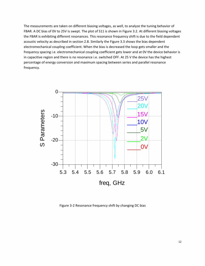
The measurements are taken on different biasing voltages, as well, to analyze the tuning behavior of
FBAR. A DC bias of 0V to 25V is swept. The plot of S11 is shown in Figure 3.2. At different biasing voltages
the FBAR is exhibiting different resonances. This resonance frequency shift is due to the field dependent
acoustic velocity as described in section 2.8. Similarly the Figure 3.3 shows the bias dependent
electromechanical coupling coefficient. When the bias is decreased the loop gets smaller and the
frequency spacing i.e. electromechanical coupling coefficient gets lower and at 0V the device behavior is
in capacitive region and there is no resonance i.e. switched OFF. At 25 V the device has the highest
percentage of energy conversion and maximum spacing between series and parallel resonance
frequency.
Figure 3-2 Resonance frequency shift by changing DC bias
5.4 5.5 5.6 5.7 5.8 5.9 6.05.3 6.1
-20
-10
-30
0
freq, GHz
S P
ara
mete
rs
___25V
___20V
___15V
___10V
____5V
____2V
____0V

13
Figure 3-3 Effect of DC bias on electromechanical coupling coefficient
3.2 Modeling
There are different models that can be used to model the FBAR. MASON, Krimholtz, Leedom and
Matthae (KLM) and BVD models are the most widely used equivalent circuits. MASON and KLM are the
physical models of FBAR but BVD model is the electrical model that consists of lumped elements.
MASON and BVD model has been used in this thesis to extract the parameters and further design of
bandpass filter. Both of the models are described below.
3.2.1 MASON MODEL Mason is the most commonly used physical equivalent circuit to model an FBAR [19]. It can be used to
analyze the pre-fabrication behavior of the device. It converts the FBAR into two acoustic ports and one
electrical port connected to the acoustic part by an electromechanical transformer. The
electromechanical transformer determines the conversion of electrical energy into acoustic energy and
vice versa as expressed by S.Sherrit et al in [11]. The MASON model is shown in figure 3.4.
freq (500.0MHz to 15.00GHz)
S1
1
_________S11_25V
_________S11_20V
_________S11_15V
_________S11_10V
_________S11_5V
_________S11_0V

14
Figure 3-4 MASON Model of an FBAR
The parameters for the MASON model are given by [11]. Za and Zc model the acoustic impedance of the
piezoelectric layer. C0 is the static capacitance between the top and bottom electrode. While ‘n’ is the
turn ratio of the electromechanical transformer that determines the energy transformation from
electrical to mechanical and vice versa.
3.1
3.2
tan(
) 3.3
3.4
where
= free space dielectric constant
= Dielectric constant of piezoelectric film
= Thickness of piezoelectric film
= Area of the resonator
while ,n ,Γ ,t and C0 are treated as complex constants and are manipulated to program the schematic
design.

15
3.2.2 Extraction of Parameters by using MASON Model The Mason model described above is used to extract the physical parameters of the piezoelectric thin
film. The Bragg reflector is cascaded by using the acoustic transmission lines with appropriate length,
impedance and propagation constant and is given in table 3.1. Generally no losses are included in the
original mason model but in this program the losses are introduced to exactly model the device
behavior. The dielectric loss has been introduced in terms of ‘G0’. While ‘Rs’ is introduced to model the
electrode losses in the electrical part of the circuit. The losses in the active layer are also introduced. The
mason model including the Bragg reflector is shown in figure 3.5.
Table 3-1 Physical Parameters of Layers used in FBAR
Layers Q Factor Acoustic Impedance (Kg/m2 s)
Acoustic Velocity (m/s)
Aluminum 500 16.98e6 6290
Platinum 100 80.2e6 3737
Titanium 100 27.3e6 6070
Titanium oxide 500 33.9e6 8477
Silicon Dioxide 500 12.55e6 5972
Hafnium Oxide 500 52.77e6 5451
Silicon 500 19.7e6 8433
Air 500 400 360

16
Figure 3-5 MASON Model with Bragg reflector

17
Tuning and optimization procedure is adapted to exactly reproduce the measured data. The highest DC
bias of 25V is selected, to first extract the physical parameters. Figure 3.6 compares the measurement
and simulation results by utilizing the MASON equivalent circuit. Figure 3.6 (a) indicates that the
extracted electromechanical coupling coefficient is in favorable comparison with measurement. Similarly
figure 6.3 (b) indicates that extracted combination of piezoelectric thickness and acoustic velocity of
table 3.2 can reproduce the measured data. The extracted physical parameters of ferroelectric thin film
are given in table 3.2.
(a)Extracted ‘ ’ vs. measured ‘ ’
(b)Extracted S11 (dB) vs. Measured S11 (dB)
Figure 3-6 Comparison of measured data with MASON simulated data
freq (500.0MHz to 15.00GHz)
S P
ara
me
ter
_____MASON Simulation
_____Measurement
m7freq=dB(recent_25V..S(1,1))=-17.372Min
5.707GHzm5freq=dB(S(1,1))=-17.408Min
5.708GHz
2 4 6 8 10 12 140 16
-15
-10
-5
-20
0
freq, GHz
S P
ara
mete
r
Readout
m7
Readout
m5
m7freq=dB(recent_25V..S(1,1))=-17.372Min
5.707GHzm5freq=dB(S(1,1))=-17.408Min
5.708GHz
_____MASON Simulation
_____Measurement

18
Table 3-2 Extracted parameters of single BSTO FBAR
Parameters Extracted Value
Top Electrode Area 314 µm2
BSTO Thickness 285 nm
Acoustic Velocity of BSTO 6978 m/s
Dielectric Constant of BSTO 102.5
Electromechanical Coupling Co-efficient 7%
3.2.3 BVD Model Butterworth and Van Dyke presented a lumped element electrical model, also known as BVD, which
models FBAR near resonance. It converts the FBAR into four equivalent lumped elements i.e. Rm, Cm, Lm
and C0. Rm, Cm and Lm are known as motional parameters, motional branch or motional arm. C0
determines the capacitance between the two electrodes with piezoelectric film sandwiched between
them. Lm represents the acoustic mass; while Cm and Rm represent the compliance and acoustic loss
respectively [2].The BVD electrical equivalent circuit and its parameters are presented here given by [1].
Figure 3-7 Butterworth Van-Dyke Model (BVD)
3.5
3.6
3.7
3.8
where
Q= Quality factor of piezoelectric film

19
3.2.4 Extraction of Parameters by using MBVD Model The original BVD model does not account the dielectric losses so another model based on the BVD model
is presented and known as Modified Butterworth -Van Dyke (MBVD) model. In this model the dielectric
loss is introduced in series of the static capacitor. The MBVD model is shown in figure 3.8 in which ‘ ’ is
representing the dielectric loss and ‘Rs’ is representing the electrode losses *20]. Cm and Lm provides the
series resonant frequency while the shunt resonant frequency is provided by Cm and Lm in series with C0
as described by [21, 22].
Figure 3-8 Modified Butterworth Van-Dyke Model (MBVD)
The physical parameters, which were extracted by using the mason model, are used to simulate and
extract the motional parameters. By using the tuning and optimization procedure the simulation is
performed to reproduce the measurements. Figure 3.9 shows that the MBVD simulations and
measurements are in good agreement.
Figure 3-9 Comparison between MBVD simulation and measured data
freq (500.0MHz to 15.00GHz)
S11
_____________Simulation
_____________Measurement
20
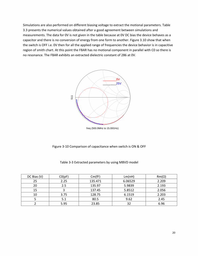
Simulations are also performed on different biasing voltage to extract the motional parameters. Table
3.3 presents the numerical values obtained after a good agreement between simulations and
measurements. The data for 0V is not given in the table because at 0V DC bias the device behaves as a
capacitor and there is no conversion of energy from one form to another. Figure 3.10 show that when
the switch is OFF i.e. 0V then for all the applied range of frequencies the device behavior is in capacitive
region of smith chart. At this point the FBAR has no motional component in parallel with C0 so there is
no resonance. The FBAR exhibits an extracted dielectric constant of 286 at 0V.
Figure 3-10 Comparison of capacitance when switch is ON & OFF
Table 3-3 Extracted parameters by using MBVD model
________0V
________25V
freq (500.0MHz to 15.00GHz)
S11
DC Bias (V) C0(pF) Cm(fF) Lm(nH) Rm(Ω)
25 2.25 135.471 6.06529 2.209
20 2.5 135.97 5.9839 2.193
15 3 137.45 5.8512 2.056
10 3.75 128.75 6.1519 2.203
5 5.1 80.5 9.62 2.45
2 5.95 23.85 32 6.96

21
4 Electrically Tunable Bandpass Filter Based on
Ferroelectric Film
Filters are the key components for separating the desired frequency from the spectrum in mobile/radio
communication systems. High data rates, greater mobility, cost effectiveness, lighter weight, smaller size
and high performance is the demand for advance mobile communication systems[23-25].Introduction
of new frequency bands for wireless communication system i.e. from 500 MHz to 6 GHz has put the
challenges on filter technology. Surface acoustic wave (SAW) filters and Ceramic filters have been used
previously. SAW filters have high selectivity and small size [4]but low power handling capability, poor
insertion loss and limited frequency operation up to 3GHz has limit the applications of SAW filters in
advanced mobile communication systems[27]. On the other hand Ceramic filters have high power
capability and good selectivity. But their large size is the major drawback for miniaturized front end
applications [26, 28].
This chapter focuses on an Electrically Tunable Bandpass filter based on BSTO Ferroelectric Film, filter
topologies, design, simulations and layout/mask design for the proposed Bandpass filter.
4.1 TFBAR Bandpass Filter TFBAR based Bandpass filter is the promising technology for the current miniature and future smart and
compact front end applications in radio communication. TFBAR filters can operate up to several GHz
range with high quality factor, high power handling capability, low insertion loss and smallest size as
compared to SAW, Lumped and ceramic filters [29-31]. DC field dependent parameters of BSTO enable
to design the tunable bandpass filters which allow agile communication [31-35].
4.2 Design Principle To design a simple bandpass filter based on FBAR it requires at least two FBARs, one is connected in
series and other is in parallel as shown in figure 4.1.
Figure 4-1 Ladder type filter [19]

22
The resonance frequency of shunt resonator is kept lower than the series resonator. The difference
between the series resonance frequency of shunt resonator and the parallel resonance frequency of
series resonator determines the bandwidth .Larger the difference between these resonance frequencies,
larger the bandwidth but a dip can appear in pass band when the gap between these resonance
frequencies is increased as described by [16, 33, and 34].
4.3 Filter Topologies There are three different topologies currently being used to design bandpass filters.
1. Ladder Type
2. Lattice Type
3. Ladder-Lattice Type
4.3.1 Ladder Type A simple ladder type filter is shown in figure 4.1 [19]. It can consist of at least two FBARs. Ladder type
filters have very sharp roll off but out of band rejection is rather poor [4]. The area of the resonators can
be optimized to get better out of band rejection. It can also be improved by cascading more stages but
this will increase the insertion loss [29, 36, and 38]. In general the ladder type filters have low insertion
loss, low out band rejection and high filtering sharpness [25, 26]
4.3.2 Lattice Type The topology by using lattice technique for filter design is shown in figure 4.2 [19].
Figure 4-2 Lattice type filter [19]
Lattice type filters have high out of band rejection but lower roll off near pass band. To improve the roll
off more resonators can be cascaded but it will increase the insertion loss. Another approach that can be
used to get sharper roll off is to optimize the static capacitance of the two arms of the lattice filter [16].

23
Generally the lattice filters have high out of band rejection, lower filtering sharpness and medium
insertion loss as compared to ladder type filters.
4.3.3 Ladder-Lattice Type The topology that combines both the ladder and lattice type in one filter is called the ladder-lattice
topology. This kind of filter can be optimized to have both the high out of band rejection and sharper roll
off near pass band [26]. An example of a ladder-lattice filter is shown in figure 4.3 [35].
Figure 4-3 Ladder-Lattice filter [19]
4.4 Design of a 3rd Order T-type Ladder filter Different filters have been studied and simulated including the π-Type and T-type techniques in ladder
topology. As the ladder type filters are being mostly used because of straightforward implementation,
lower insertion loss and high out of band rejection [17, 24, 27, and 28] so a 3rd order T-type ladder filter,
as shown in figure 4.4, has been selected to work further and optimize it to get the best performance.
The order of the filter indicates the total number of resonators in the filter. The series resonators are
identical to each other in terms of resonator area, BSTO layer thickness and electrode thicknesses. Both
series resonators also have the same resonance frequency. While the shunt resonator is tuned at lower
frequency than the series resonator. To get the different resonant frequency the thickness of the
piezoelectric film can be optimized [24] or the mass loading of the top electrode can be processed during
fabrication [13,21]. In this work the mass loading of the top electrode is used to tune the resonant
frequency of the shunt resonator. Each resonator has been modeled by using the MBVD model and then
these MBVD equivalent circuits are used to design and simulate the bandpass filter. The loading layer
thickness has been achieved by using the MASON model.

24
Figure 4-4 3rd order ladder filter
4.4.1 Schematic Simulation and Results
4.4.2 Schematic Simulation A 3rd order T-Type ladder filter by using MBVD equivalent circuit is shown in figure 4.5. There are three
resonators in the circuit. Each MBVD circuit is representing an FBAR. The series resonators have the
same resonant frequency. But the shunt resonator has been tuned to have the resonance frequency
lower than the series resonator. The filter is designed to operate on a 50 Ω system. To achieve the
maximum bandwidth the resonance frequency of shunt resonator has been optimized. As described
earlier that a dip can appear in the pass band if the difference between the resonance frequencies is
continuously increased so the optimization of resonance frequency of shunt resonator is kept limited to
avoid the dip in pass band. The area of the resonators is tuned to achieve the minimum insertion loss
and high out of band rejection. A trade off in between insertion loss and out of band rejection has been
observed so after optimization the size of the resonators providing the minimum achievable insertion
loss and out of band rejection is given in the table 4.1. The table also includes the calculated values of
motional arms, top electrode thicknesses and resonance frequency of each resonator.

25
Figure 4-5 MBVD equivalent circuit of bandpass filter
Table 4-1 Calculated MBVD and physical parameters of designed bandpass filter
Parameter Series Resonator Shunt Resonator
Area (µm2 ) 12*12 17*17
Series Resonance Frequency(GHz) 5.723 5.552
C0(pF) 0.4976 0.8474
Rm (Ω) 9.477 5.913
Cm(fF) 28.044 47.76
Lm(nH) 27.577 17.205
Top electrode Thickness (nm) 78 100

26
The simulation result of a 3rd order ladder type TFBAR bandpass filter is shown in figure 4.6. The designed
filter has the insertion loss of –2.925 dB. The out of band rejection of -10dB and a 3dB bandwidth of
176MHz have been achieved. Both the resonators have two resonant frequencies. The pass band
depends on the difference between the series resonant frequency of the series resonator and the
parallel resonant frequency of shunt resonator. While beyond these frequencies each resonator behaves
like a capacitor. Maximum transmission occurs when the series resonance frequency of the series FBAR
equals or near to the parallel resonance frequency of the shunt FBAR. At series resonance frequency of
shunt FBAR and parallel resonance frequency of series FBAR, the transmission is blocked thus results in a
bandpass filter as demonstrated in figure 4.7. Due to the field dependent parameters of BSTO the filter
can be switched OFF and ON by changing the bias voltages. Also the center frequency of the filter can be
tuned by varying the DC bias.
Figure 4-6 Simulation result for a 3rd order T-Type Ladder Filter

27
Figure 4-7 working principle of FBAR bandpass filter
The figure 4.8 compares the transmission and reflection coefficients when the switch is OFF & ON
respectively. Figure 4.8 (a) indicates that when the switch in OFF there is no resonance but at 25V DC
bias i.e. the highest selected voltage the filter exhibits a resonance. Similarly at 0V bias there is no
transmission of frequencies but at 25 V the device is ON and gives a bandpass response with some
transmission loss while beyond this pass band the filter exhibits the high transmission loss.
(a) S11 (dB) (b) S21 (dB)
Figure 4-8 Parameters at 0V & 25V Bias
28
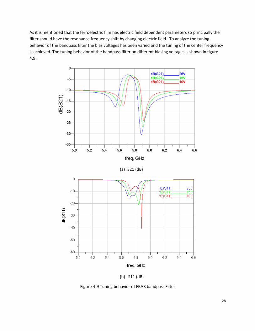
As it is mentioned that the ferroelectric film has electric field dependent parameters so principally the
filter should have the resonance frequency shift by changing electric field. To analyze the tuning
behavior of the bandpass filter the bias voltages has been varied and the tuning of the center frequency
is achieved. The tuning behavior of the bandpass filter on different biasing voltages is shown in figure
4.9.
(a) S21 (dB)
(b) S11 (dB)
Figure 4-9 Tuning behavior of FBAR bandpass Filter

29
4.5 Layout Design and Electromagnetic Co- Simulation
When the simulation results are achieved and physical parameters i.e. area and thickness of each layer is
known then it comes to design the layout. This section will provide the details about the designed layout
of the filter. Later this layout will also be used for electromagnetic co-simulation.
4.5.1 Layout Design Different layout patterns were designed and discussed regarding fabrication and finally a layout is
presented here in figure 4.10 which is designed by using the ADS momentum. The total area of the filter
including grounds and pads for measurements is 550*400 µm2. The layout is designed to measure by
using ground-signal-ground (GSG) probes with the size of 150 µm. As the filter contains multiple set of
layers so at some points it is needed to pattern some layers. It is also necessary to pattern the layers
because the area that will be sandwiched between top and bottom electrode will be the active area
therefore it can be seen that three resonators are obvious in layout. The pattern of each layer is
presented in Appendix. The layout is marked with some text and points which describes the each part of
the layout. Part of the layout marked with ‘A’ and ‘B’ will be used to connect the ground and signal
probes respectively. DC bias will be applied to the point marked with ‘C’. The point ‘D’ is indicating the
isolation layer between top and bottom electrode.
Figure 4-10 Layout of the filter

30
4.5.2 Electromagnetic Co-Simulation To analyze the effect of parasitic capacitances between FBARs momentum simulation is performed. For
momentum simulation the layout that is presented above is updated with layer thicknesses and
substrate definition. After defining the layers and substrate the MBVD motional parameters are
connected to the layout in the schematic window. To connect the motional parameters it is necessary to
define the ports in momentum. So after defining the ports in momentum the layout is imported in
schematic window and motional arm is connected. Normally the layout without the motional branch is
just a capacitor as there is a dielectric between electrodes so it is necessary to introduce the motional
arm in schematic. The complete layout with motional parameters connected is shown in figure 4.11.
Figure 4-11 Layout with motional branch for Electromagnetic Co simulation
31
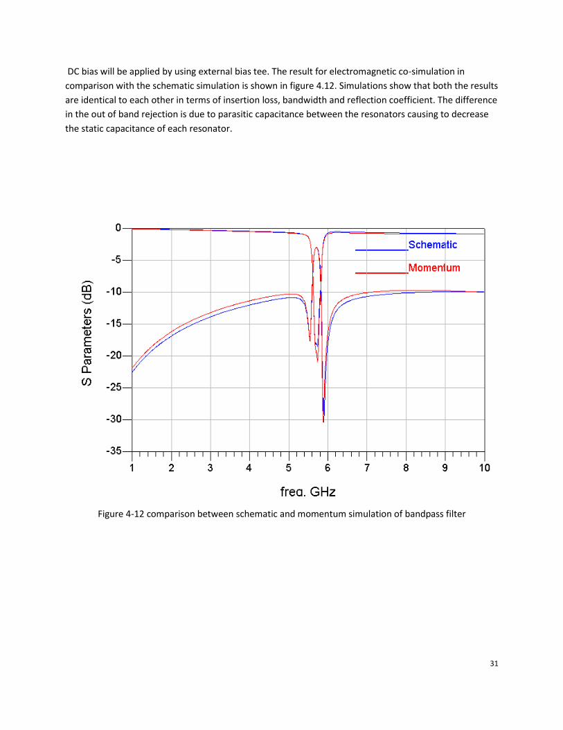
DC bias will be applied by using external bias tee. The result for electromagnetic co-simulation in
comparison with the schematic simulation is shown in figure 4.12. Simulations show that both the results
are identical to each other in terms of insertion loss, bandwidth and reflection coefficient. The difference
in the out of band rejection is due to parasitic capacitance between the resonators causing to decrease
the static capacitance of each resonator.
Figure 4-12 comparison between schematic and momentum simulation of bandpass filter

32
4.5.3 Masks Design for Fabrication Masks are designed in ADS momentum. A silicon substrate of 10*10mm2 has been chosen. Masks
contain the filters and resonators, both series and parallel, separately. Some test structures are inserted
for future measurements and de embedding. Masks for each patterned layer are shown in Appendix.
Each layer will be deposited as it is patterned and piezoelectric layer will be deposited all over the
substrate. The final structure of the mask designed on a 10*10mm2 wafer is shown in figure 4.13.
Figure 4-13 Final Mask on 10*10 mm2 wafer

33
5 Conclusion and future work
5.1 Conclusion This thesis work utilized the electric field dependent parameters of BSTO ferroelectric film and
successfully designed and simulated an electrically tunable bandpass filter.
A single FBAR based on BSTO ferroelectric film is measured and modeled by using MASON and MBVD
model. Piezoelectric constants are extracted. Different FBAR filter topologies are studied and simulated.
A 3rd order T-Type ladder based tunable bandpass filter is designed and simulated by using the extracted
piezoelectric constants and MBVD model. Mass loading of top electrode is used to change the resonant
frequency of series resonators from shunt resonator.
The insertion loss of -2.925 dB is achieved. The designed filter exhibits 3dB bandwidth of 176 MHz and
out of band rejection of -10.807 dB. Momentum simulation is also performed and comparable results
have been achieved in layout design and schematic simulation.
5.2 Future work The study and simulations has shown that electrically tunable bandpass filters can be achieved by using
the ferroelectric films so first the future work will involve the manufacturing of the designed bandpass
filter. The resonators used to design the bandpass filter will be measured separately for de-embedding.
Electrode materials can be changed to get higher coupling coefficient. Filter design by using two different
piezoelectric thicknesses can also be implemented. Mass loading of bottom electrode can be suggested
which will decrease the processing of layer depositions on the ferroelectric film. Ladder-lattice filter
topology can be used to achieve the goals for particular bandwidth, insertion loss and out of band
rejection.
34
6 References [1] J. F. Rosenbaum, Bulk Acoustic Wave Theory and Devices (ArtechHouse, Boston, 1988).
[2] W. Pan, “A surface micromachined tunable film bulk acoustic resonator,” Proceedings of SPIE,
vol. 5455, 2004, pp. 166-173.
[3] R. Lanz and P. Muralt, “Bandpass filters for 8 GHz using solidly mounted bulk acoustic wave
resonators.,” IEEE transactions on ultrasonics, ferroelectrics, and frequency control, vol. 52, Jun. 2005, pp.
936-46.
[4] A.A. Shirakawa, J. Pham, P. Jarry, and E. Kerherve, “Design of FBAR Filters at High Frequency
Bands,” International Journal of RF and Microwave Computer-Aided Engineering, 2006, pp. 115-122.
[5] J. Bjurström, “Advanced Thin Film Electroacoustic Devices,” 2007.
[6] B. Ha, I. Song, Y. Park, D. Kim, W. Kim, K. Nam, and J. Pak, “Novel 1-chip FBAR filter for wireless
handsets,” Sensors and Actuators A: Physical, vol. 130-131, Aug. 2006, pp. 247-253.
[7] J. Berge, A. Vorobiev, W. Steichen, S. Gevorgian, and S. Member, “Tunable Solidly Mounted Thin
Film Bulk Acoustic Resonators Based on Ba x Sr 1 x TiO 3 Films,” Components, vol. 17, 2007, pp. 655-657.
[8] P.B. Kirby, Q.X. Su, E. Komuro, Q. Zhang, M. Imura, and R.W. Whatmore, “PZT thin film bulk
acoustic wave resonators and filters,” Proceedings of the 2001 IEEE International Frequncy Control
Symposium and PDA Exhibition (Cat. No.01CH37218), 2001, pp. 687-694.
[9] A. Noeth, T. Yamada, P. Muralt, A.K. Tagantsev, and N. Setter, “Tunable thin film bulk acoustic
wave resonator based on Ba(x)Sr(1-x)TiO3 thin film.,” IEEE transactions on ultrasonics, ferroelectrics, and
frequency control, vol. 57, Jan. 2010, pp. 379-85.
[10] P. Turalchuk, I. Vendik, O. Vendik, and J. Berge, “Electrically Tunable Bulk Acoustic Filters with
Induced Piezoelectric Effect in BSTO Film,” 2008 38th European Microwave Conference, Oct. 2008, pp.
1695-1698.
[11] S. Sherrit, S.P. Leary, B.P. Dolgin, and Y. Bar-Cohen, “Comparison of the Mason and KLM
equivalent circuits for piezoelectric resonators in the thickness mode,” 1999 IEEE Ultrasonics Symposium.
Proceedings. International Symposium (Cat. No.99CH37027), pp. 921-926.
[12] Y. Satoh, T. Nishihara, T. Yokoyama, M. Iwaki, and T. Miyashita, “Development of 5GHz FBAR
Filters for Wireless Systems,” Design, pp. 5-8.
[13] G.Rupprecht and W.H.Winter,’’Electromechanical Behavior of Single-Crystal Strontium Titanate,’’
Phy. Rev., vol. 155, pp. 1019-1028, 1967.
35
[14] S. Gevorgian, a Vorobiev, and T. Lewin, “dc field and temperature dependent acoustic
resonances in parallel-plate capacitors based on SrTiO[sub 3] and Ba[sub 0.25]Sr[sub 0.75]TiO[sub 3]
films: Experiment and modeling,” Journal of Applied Physics, vol. 99, 2006, p. 124112.
[15] W. Pang, H. Zhang, H. Yu, C.-yuan Lee, E.S. Kim, and S. Member, “Acoustic Resonator,” vol. 16,
2007, pp. 1303-1313.
[16] X. Zhu, J.D. Phillips, A. Mortazawi, and A. Arbor, “A DC Voltage Dependant Switchable Thin Film
Bulk Wave Acoustic Resonator Using Ferroelectric Thin Film,” 2007, pp. 671-674.
[17] G.N. Saddik, D.S. Boesch, S. Stemmer, and R. a York, “dc electric field tunable bulk acoustic wave
solidly mounted resonator using SrTiO [sub 3+,” Applied Physics Letters, vol. 91, 2007, p. 043501.
[18] A. Volatier, E. Defa , M. A d, A. N’hari, P. Ancey, and B. Dubus, “Switchable and tunable
strontium titanate electrostrictive bulk acoustic wave resonator integrated with a Bragg mirror,” Applied
Physics Letters, vol. 92, 2008, p. 032906.
[19] Y.-dae Kim, S. Member, K.-hyun Sunwoo, S.-chul Sul, J.-ho Lee, D.-hwan Kim, I.-sang Song, S.-
hoon Choa, and J.-gwan Yook, “Highly Miniaturized RF Bandpass Filter Based on Thin-Film Bulk Acoustic-
Wave Resonator for 5-GHz-Band Application,” vol. 54, 2006, pp. 1218-1228.
[20] K.-wook Kim, S. Member, M.-gweon Gu, and J.-gwan Yook, “Resonator Size Effects on the TFBAR
Ladder,” Components, vol. 13, 2003, pp. 335-337.
[21] J.Y. Park, H.C. Lee, and S.J. Cheon, “DESIGN AND FABRICATION OF INTEGRATED FILM BULK
ACOUSTIC RESONATOR AND FILTER ON SILICON NITRIDE MEMBRANE,” Microwave and Optical
Technology Letters, vol. 48, 2006, pp. 2230-2233.
[22] S.-H. Zhao, S.-R. Dong, H.-J. Zhang, W.-W. Cheng, and X.-X. Han, “Modeling of RF filter
component based on film bulk acoustic resonator,” IEEE Transactions on Consumer Electronics, vol. 55,
May. 2009, pp. 351-355.
[23] T. Nishihara, T. Yokoyama, T. Miyashita, and Y. Satoh, “High Performance and Miniature Thin
Film Bulk Acoustic Wave Filters for 5 GHz,” Design, vol. 00, 2002, pp. 969-972.
[24] P.-yen Chen, Y.-chung Chin, H.-hung Lin, and C.-li Hou, “A Systematic Design Method for Band-
Pass Filters Composed of Film Bulk Acoustic Resonators,” Electronics, pp. 3-5.
[25] H.P. Loebl, C. Metzmacher, R.F. Milsom, P. Lok, F.V.A.N. Straten, and A. Tuinhout, “RF Bulk
Acoustic Wave Resonators and Filters,” Architecture, 2004, pp. 109-118.
[26] M.E. Hassan, E. Kerherve, Y. Deval, A.A. Shirakawa, and P. Jarry, “A STUDY ON FBAR FILTERS
RECONFIGURATION,” Elements, pp. 0-3.
[27] H. Zhang, S. Dong, W. Chen, Y. Han, and A.M. Fbar, “MIMO Multiplexer Based on Film Bulk
Acoustic Resonator,” Current, 2010, pp. 805-810.

36
[28] A.A. Shirakawa, J.-m Pham, P. Jarry, E. Kerherve, F. Dumont, J.-b David, and A. Cathelin, “A High
Isolation and High Selectivity Ladder-Lattice BAW-SMR Filter,” Response, vol. 0, 2006, pp. 905-908.
[29] F.Z. Bi and B.P. Barber, “Frank Z. Bi and Bradley P. Barber,” October, 2008, pp. 65-80.
[30] D. Shim, Y. Park, K. Nam, S. Yun, D. Kim, A. Design, and F. Block, “Ultra-miniature Monolithic
FBAR Filters for Wireless Applications,” vol. 1, 2005, pp. 213-216.
[31] H. Jin, S.R. Dong, and D.M. Wang, “Design of Rx Filter for WCDMA Direct-Conversion Front-End
Using FBAR Technology,” Symposium A Quarterly Journal In Modern Foreign Literatures.
[32] G.N. Saddik, D.S. Boescht, S. Stemmert, and R.A. York, “Acoustic Wave Solidly Mounted
Resonator,” Nonlinearity, vol. 93106, 2008, pp. 1263-1266.
[33] J. Verdu, “LADDER-TYPE FILTER BASED ON BULK ACOUSTIC WAVE RESONATORS WITH IMPROVED
OUT-OF-BAND,” Microwave and Optical Technology Letters, vol. 50, 2008, pp. 103-107.
[34] G.G. Fattinger, J. Kaitila, R. Aigner, W. Nessler, and T. Ag, “Thin Film Bulk Acoustic Wave Devices
for Applications at 5GHz,” Ultrasonics, vol. m, 2003, pp. 174-177.
[35] S. Giraud, S. Bila, M. Chatras, D. Cros, and M. Aubourg, “Communication Terminals,” Ultrasonics,
vol. 57, 2010, pp. 52-58.
[36] K.-wook Kim, G.-yong Kim, J.-gwan Yook, and H.-kyu Park, “Air-gap–type tfbar-based filter
topologies,” Microwave and Optical Technology Letters, vol. 34, 2002, pp. 386-387.
[37] O. Men, “PROCEDURE FOR THE DESIGN OF LADDER BAW FILTERS TAKING ELECTRODES INTO
ACCOUNT,” Electromagnetics, vol. 7, 2009, pp. 127-137.
[38] B. Ha, I. Song, Y. Park, D. Kim, W. Kim, K. Nam, and J. Pak, “Novel 1-chip FBAR filter for wireless
handsets,” Sensors and Actuators A: Physical, vol. 130-131, Aug. 2006, pp. 247-253.

37
7 Appendix This section shows the MBVD parameters, electromechanical coupling coefficient and Q-factor plots with
respect to applied DC bias. Also the pattern of the masks for each layer is given here. The complete
layout for a bandpass filter is presented. Finally the filter and test structure mask is shown to fabricate
on 10*10 mm wafer.
Figure 7-1 Coupling Coefficient vs. DC Bias
(a)Motional Capacitance vs. DC Bias
0 5 10 15 20 250
1
2
3
4
5
6
7
8
X: 25
Y: 7.12
Voltage (V)
Coupling C
oeff
icie
nt
kt2
%)
Coupling Coefficient vs DC bias
X: 20
Y: 6.42
X: 15
Y: 5.46
X: 10
Y: 4.12
X: 5
Y: 2.08
X: 2
Y: 1.03
0 5 10 15 20 250
20
40
60
80
100
120
140
X: 25
Y: 135.5
Voltage (V)
Motional C
apacitance (
fF)
Motional Capacitance vs DC bias
X: 20
Y: 136
X: 15
Y: 137.4X: 10
Y: 128.8
X: 5
Y: 80.5
X: 2
Y: 23.85
X: 0
Y: 4.99

38
(b)Motional Inductance vs. DC Bias
(c)Motional Resistance vs. DC Bias
0 5 10 15 20 250
20
40
60
80
100
120
140
160
X: 0
Y: 152
Voltage (V)
Motional In
ducta
nce (
nH
)
Motional Inductance vs DC bias
X: 2
Y: 32
X: 5
Y: 9.62
X: 10
Y: 6.152
X: 15
Y: 5.851
X: 20
Y: 5.839
X: 25
Y: 6.065
0 5 10 15 20 250
50
100
150
200
250
X: 0
Y: 250
Voltage (V)
Motional R
esis
tance (
Ohm
)
Motional Resistance vs DC bias
X: 2
Y: 6.96
X: 5
Y: 2.45
X: 10
Y: 2.023
X: 15
Y: 2.056
X: 20
Y: 2.193
X: 25
Y: 2.209

39
Figure 7-2 Motional Parameters vs. DC Bias
Figure 7-3 Extracted Q factor vs. DC Bias
0 5 10 15 20 2550
60
70
80
90
100
110
120
X: 25
Y: 93.64
Voltage (V)
Qs &
Qp
Qs & Qp vs DC bias
X: 20
Y: 92.53
X: 15
Y: 95.68
X: 10
Y: 99.08
X: 5
Y: 112.4
X: 2
Y: 65.52
X: 2
Y: 50.33
X: 5
Y: 78.15
X: 10
Y: 66.26 X: 15
Y: 64.46X: 20
Y: 63.91
X: 25
Y: 64.92
Qs
Qp

40

41

42
Figure 7-4 MASK set for Fabrication
Figure 7-5 Final Design of the Filter