depfet pixel vertex detector for the ilc - desy · pdf filedepfet pixel vertex detector for...
TRANSCRIPT

DESY PRC R&D 03/01 Update 2(07)Project: DEPFET for ILCType of Document: Status ReportDate: 17.4.2007Verision: 2.0
DEPFET Pixel Vertex Detector for the ILC
L. Feld1, R. Jussen, W. Karpinski, K. Klein(1. Physikalisches Institut, RWTH Aachen, Germany)
P. Hettkamp, R. Kohrs, M. Karagounis, M. Koch, H. Kruger, P. Lodomez,M. Mathes, L. Reuen, C. Sandow, J. Schneider, E. von Torne, M. Trimpl,
J. Velthuis, N. Wermes2
(Bonn University, Germany)
W. de Boer3, J. Bol, A. Sabellek(Universitat Karlsruhe, Germany)
P. Fischer4, F. Giesen, C. Kreidl, I. Peric(Mannheim University, Germany)
L. Andricek, X. Chen, A. Frey, K. Heinzinger, P. Lechner, G. Lutz,H. G. Moser5, R. H. Richter, M. Schnecke, A. Raspereza, S. Rummel,
L. Struder, J. Treis(MPI fur Physik, Munich, Germany)
Z. Dolezal, Z. Drasal, P. Kodys6, D. Scheirich(Charles University, Prague, Czech Republic)
I. Carbonell, J. Fuster, C. Lacasta7, M. Vos(Instituto de Fisica Corpuscular (IFIC), CSIC-UVEG, Valencia, Spain)
[email protected]@[email protected]@[email protected]@[email protected]

Abstract
DEPFET pixels offer a unique possibility for a high resolution pixel vertexdetector as the innermost component of the tracking system in an ILC de-tector. The key idea of DEPFET sensors is the integration of amplifyingtransistors into a fully depleted bulk in such a way that all signal charges arecollected in the ’internal gates’ of the transistors. The excellent noise per-formance obtained through the low input capacitance in combination withthe full signal from the depleted bulk leads to a large S/N ratio. The sen-sor itself can therefore be made very thin (50µm) without loss of efficiency.Readout is performed by cyclic enabling of transistor rows in a large ma-trix. The total system, including readout and sequencing chips, is expectedto dissipate less than 10 W for a five layer geometry assuming a 1:200 powerduty cycle.In this status report the progress of the DEPFET development towards anILC vertex detector with respect to the last PRC review in May 2005 ispresented. Since then properties of prototype matrices and dedicated ASICelectronics have been characterized in various laboratory and test beammeasurements. In particular a point resolution of less than 2 µm has beendemonstrated (using 450 µm thick sensors). Based on these results largermatrices, improved readout and control electronics have been designed whichare presently in production. These second generation systems will showlarger gain, reduced system noise and almost ILC size. Further technologi-cal development includes the thinning technology, now routinely done on 6”wafers and preparation for bump bonding. In parallel software was devel-oped to simulate the performance of a DEPFET based vertex detector inan ILC detector.
2

1 Introduction
This status report summarizes the progress achieved towards a DEPFETpixel vertex detector suited for application at the ILC. The initial R&D,described in the PRC report from May 2003, was oriented towards TESLA[1]. The anticipated environment at ILC [2] is very similar and the assumedboundary conditions remain valid. The general requirements for a vertexdetector in the high multiplicity environment of the ILC and how they areaddressed by a DEPFET system are summarized as follows:
. Aim at a spatial point resolution per layer of . 4µm. This can beachieved by pixels of 25×25 µm2 size guaranteeing a binary resolutionof 25µm/
√12 ≈ 7µm. Analog interpolation assuming an anticipated
signal to noise ratio of & 40 will significantly improve this value to. 3.5µm (R− φ) and . 4µm (z). Using a GEANT4 simulation it canbe demonstrated that the required impact parameter resolution of [19]
σ(IPr−φ) = 5µm⊕ 10µm
p · sin3/2 θ,
can be met with such a pixel layout. With 450 µm thick detectors aresolution below 2 µm has already been achieved in test beams.
. The innermost layer is at a radius of ≈ 15mm. The active area inthis innermost layer must therefore have a length (along the beam) of≈ 10 cm. This requires 4096× 512 pixels of 25µm× 25µm.
. The innermost layer should tolerate an accumulated radiation doseafter 5 years of operation of 200 krad. Irradiation tests of DEPFETdevices suggest that the sensors are radiation tolerant well above thislimit.
. Minimum radiation length should restrict multiple scattering. Thedesign goal is to reach in the order of 0.1% of a radiation length permodule. A thinning technology compatible with DEPFET productionhas been developed. It can be used to build an all silicon sensor modulewith a thickness in the active part of 50µm. Due to the low noisecharacteristics of the DEPFET a signal to noise ratio > 40 is stillachievable with such a module.
. Operation at a bunch train repetition rate of 5Hz with each train de-livering 2820 bunches during≈ 1ms. Assuming that the low duty cycleof 1:200 given by ILC can be exploited the average power dissipationof the system will be well below 10 W.
. A hit multiplicity of ≈ 0.03 hits per mm2 and bunch at√
s = 500 GeVmust be tolerated. In a recent study [3] this value approaches 0.04 hitsper mm2 and bunch for the nominal ILC layout with 14 mrad crossing
1

angle. In other layouts of the ILC interaction region it can even dou-ble. Assuming 30% double hits and pixels of 25× 25µm2 size the hitoccupancy in one train will be about 10%. This occupancy is proba-bly unacceptable for cluster reconstruction and pattern recognition sothat a sensor operated this close to the beam must be read out severaltimes during one bunch train. A line readout rate of 40 MHz woulddecrease the occupancy by a factor of 20 to half a percent (for a sensorwith 4096 pixels read out at both ends).
. Operation in a magnetic field of 3-5 T. The effect of the Lorentz angleis expected to be small due to the thin sensor.
The status of the project as reported in the PRC review in May 2005 [25]was:
. Small (64 × 128 pixel) DEPFET matrices with close to ILC pixelsizes (32 µm × 24 µm) had been produced successfully at the MPIsemiconductor laboratory.
. Single pixels had been successfully operated in laboratory setups. Lownoise and complete, fast clear had been demonstrated [12].
. A 128 channel readout chip (CURO) had been designed and produced.The chip operated in stand alone mode with the required rate.
. A 2 × 64 channel control chip (Switcher II) needed to switch theDEPFET gate and clear contact had been designed and produced.The chip works at the required frequency.
. A system made of a 64 × 128 DEPFET Matrix, CURO and SwitcherII had been built and operated successfully in the laboratory and in abeam test. However, the required noise performance and system speedhad not yet been achieved
. DEPFET pixels had been irradiated up to 1 Mrad and were still op-erational.
. The thinning process had been developed on 4” wafers. Using diodesit could be demonstrated that basic properties of a sensor did notdeteriorate during the thinning process.
The main goals since the last PRC review in may 2005 were:
. Radiation tests of the ASIC electronics and further tests of the DEPFETwith different particle types.
. Carry out a rigorous test beam program to assess the performance ofthe full DEPFET system in a particle environment, preferentially inhigh energy beams at CERN.
2

. Determine the limits of noise and readout speed of the present system.
. Design a new generation of readout chips adapted to the known pa-rameters of the matrices favoured by the test program.
. Prepare for the construction of a 512 × 512 close to full size systemwith multiple readout chips.
. Enlarge the collaboration.
Almost all of these goals have been achieved or are close to being achieved.They will be detailed in the following sections. The report is organized asfollows: Section 2 describes the DEPFET sensor. After a short introductionof the operation principle, the production technology and some of the imple-mented structures are described. Section 3 describes the ASIC electronicsfor control and readout. Section 4 proposes a system for operation at ILC.Results form laboratory tests and beam tests are summarized in Section 5,including radiation hardness studies in Section 5.2. In section 6 softwaredevelopment is described. The simulation software is especially useful toextrapolate the performance to ILC conditions using parameters extractedfrom beam tests. In section 7 an overview on new developments presentlyin production is given. A summary and outlook is given in Section 8.
2 The DEPFET Sensor
2.1 DEPFET Principle and Operation
The DEPleted Field Effect Transistor structure, abbreviated DEPFET, pro-vides detection and amplification properties jointly. The concept was pro-posed in 1987 [4] and developed to a level of maturity in the nineties [5–8].
The DEPFET principle of operation is shown in Figure 1. A MOSor junction field effect transistor is integrated onto a detector substrate.By means of sidewards depletion [9] and additional n-implants below thetransistor a potential minimum for electrons is created underneath (≈ 1µm)the transistor channel. This can be considered as an internal gate of thetransistor. A particle entering the detector creates electron-hole pairs in thefully depleted silicon substrate. While the holes drift into the rear contact ofthe detector, the electrons are collected in the internal gate where they arestored. The signal charge leads to a change in the potential of the internalgate, resulting in a modulation of the channel current of the transistor.
The simultaneous detection and amplification feature makes DEPFETpixel detectors very attractive for low noise operation [10, 11] and hencevery large S/N. In the case of the ILC the use of very thin (50µm) detectors(see sect. 3.4) operated with very low power consumption (see sect. 4.1) isplanned. The low noise, even at room temperature, is obtained becausethe capacitance of the internal gate is very small, much smaller than the
3

Figure 1: The DEPFET detector and amplification structure is based onplanar p-channel MOSFET structure on a completely depleted substrate. Adeep n-implant forms a potential minimum for electrons which are collectedthere. The accumulated charge in this internal gate modulates the transistorcurrent. The charge can be removed by the clear contact.
pixel cell area which governs the capacitance of standard pn-junction pixelsin hybrid pixel detectors. Furthermore, no external connection circuitry tothe first amplification stage is needed. External amplification enters only atthe second level stage. The pixel delivers a current signal which is roughlyproportional to the number of collected electrons in the internal gate. Signalelectrons as well as electrons accumulated from bulk leakage current mustbe removed from the internal gate after readout. Clearing, i.e. the removalof charges from the internal gate, is performed by periodically applying apositive voltage pulse to a clear contact. The potential barrier between theinternal gate and the clear contact can be lowered by an additional clear-gate which may be held at constant potential but which may also be pulsed.For individual pixel structures with full charge collection, the best noisevalue measured so far at room temperature is 1.6 e− (see Figure 2).
For the ILC, where speed is the driving element, a total noise contri-bution of .100 e−, including noise from the DEPFET sensor and from thereadout chip, is the realistic goal. As the output of a DEPFET is a current,further processing of the signal is current based. This also allows high-speed on-chip pedestal subtraction, simply by subtracting two – signal andpedestal – currents (see sect. 3.1).
2.2 DEPFET Operation
In a real detector a single DEPFET pixel will be operated as follows:
4

Figure 2: Fe55 spectrum obtained using a linear DEPFET single pixel inILC layout at room temperature and 10µs shaping time. The rms noise of1.6 e− is obtained from the width of the pedestal.
. The DEPFET is switched off. In this state the transistor consumesalmost no power, however, the pixel is sensitive to ionizing particles.Electrons generated by ionisation in the depleted bulk will drift to-wards the internal gate and accumulate there.
. During a readout cycle a voltage (above the transistor threshold) isapplied to the external gate, switching on the transistor. The source-drain current, composed of a pedestal current defined by the externalgate and a signal current, proportional to the charge in the internalgate, is measured.
. A voltage is applied to the clear contact, removing completely thesignal charge in the internal gate.
. Now the current is measured again, this time measuring the pedestalcurrent. In an external readout circuit this pedestal is subtracted fromthe first reading, the difference giving the signal.
. The external gate voltage is set back, switching off the transistor.
5

Figure 3: Schematics of a DEPFET matrix. Drains reading the current areconnected column wise to a readout chip. Gates and clears are connectedrow wise to switcher chips. The switcher steps through the rows while allpixels of a row are read in parallel.
This sample-clear-sample cycle is planned to be as short as 50 ns. In apixel detector the pixels will be arranged in columns and rows (see Figure 3).All transistor drains of a column are connected to one amplifier node. Thegate contacts and clear contacts are connected row wise, thus all pixelsin a row can be read and cleared in parallel. In a rolling shutter modereadout, one row is switched on and all pixels of this row are read (sample-clear-sample cycle) in parallel. Then this row is switched off and the nextrow is read and so forth until all rows have been read and the cycle startsagain. This way the readout of a complete frame8 needs about 50 µs. Thisscheme resembles the readout of a column parallel CCD, the signals areread out sequentially by a chip at the periphery. But unlike in an CCD nocharge transfer is needed and only one row is electrically active. Actually,it is possible to address each pixel individually. Hence the sensor couldbe divided into different sections which are read with different frame rates,e.g. if the background occupancy is inhomogeneous. Even a triggered ROI(region of interest) readout can be realized.
8In our design proposal (sect 4) a frame of the innermost ladder has 1024 rows
6

2.3 PXD4 Pixel Production
In 2004 the first prototype DEPFET matrices were produced. The produc-tion (dubbed PXD4) was made on high ohmic unthinned (450 µm thick)high resistivity 6” FZ wafers. Double poly and double metal technology wasintroduced into the process line to build the complex DEPFET matriceswith FET and clear gates and crossed contact lines (Figure 4). The largestmatrices contained 64 × 128 pixels. On the same wafers prototype matricesfor x-ray imaging (large circular pixels) for astrophysics use were produced.The production contained several variants, e.g. using different clear struc-tures. To improve the clear behavior, an extra high energy implant (HE)was implemented in some matrices. This has the disadvantage that the dis-tance between the potential minimum where the charge is collected and thechannel increases leading to a smaller gain.
Figure 4: Cross section through an DEPFET pixel.
An interesting feature is the double pixel. Two pixels in adjacent rowsshare the same clear structure and their transistor gates are connected to-gether. On the other hand the drain readout lines (for the signal readout)are routed in separate columns. This allows a very compact design resultingin small pixels sizes. For practical operation it has the advantage that tworows are read out in parallel, thus virtually doubling the readout speed. Theprice to pay is twice the number of readout lines.
3 The Readout and Control ASIC
As explained in the previous section two ASIC chips are necessary to oper-ate a DEPFET matrix: Firstly a switcher chip which generates row wise thevoltages needed to switch on the transistor and activates the clear. Secondlya chip reading out the current signal of all columns in parallel. The latter
7

should automatically subtract the pedestal in the sample-clear-sample cycleand store the result. Furthermore, it could perform 0-suppression, clusterfinding and sparse readout, eventually digitizing the data on chip.A complete system needs in addition a controller, which synchronizes switcherand readout chips.
3.1 The CURO Readout Chip
A fast operation as required at the ILC was the major design goal for thereadout chip [16]. Therefore, signal processing (e.g. pedestal subtraction,signal storage and compare) on the chip is done in a current-mode operationperfectly adapted to the current signal of the DEPFET device. Further-more, a subtraction of two signals as needed for the pedestal subtractioncan be done very fast and accurate with currents. By means of the pedestalsubtraction described above a fast correlated double sampling is performedsuppressing the 1/f noise contribution of the sensor. The 128 channel chipoffers the possibility of zero-suppression and sparse readout. All hits in arow are found by comparison to programmable and trimmable thresholds.The analog amplitudes as well as the digital hit pattern are stored in amixed signal memory. The digital hit pattern is scanned by a fast hit finder.The addresses of the hits are stored in a RAM for later readout, the corre-sponding analog amplitudes are multiplexed to off-chip ADCs (which couldbe integrated onto the chip in a later version). The address RAM can beread during the long bunch pause. The addresses are then associated tothe digitized values. The CURO chip has been fabricated using a 0.25µmprocess. Radiation tolerance for the doses expected at the ILC is thereforenot considered to be a critical issue. The hit detection and zero suppression(i.e. the digital part) has been operated successfully at more than 100 MHz.The analog part (double correlated sampling, current comparison) has beentested up to a row rate of 25MHz with sufficient accuracy. The intrinsicnoise contribution of the sampling in the chip at this speed has been mea-sured to be 100 nA. This is somewhat in disagreement with the calculatedvalue (about a factor of two larger [16]). For the present DEPFET deviceswith a charge to current gain of up to gq ≈ 400 pA/ e−, this translates to anoise contribution of the fast readout of ENC = 250 e−.
3.2 The Switcher II Control Chip
The SWITCHER-II9 chip is used to apply suited potentials to the rows ofthe matrix. Three signals are required in the prototype devices: externalgate, clear and clear-gate, the latter being probably not required for futuredesigns. One SWITCHER can provide two voltages for 64 channels. Thei-th channels is first selected by an internal counter. An on-chip sequencer
9a previous, low speed version in a different technology was used for slower matrices
8

is used to connect the outputs to externally supplied voltages by means ofsimple analog multiplexers in an arbitrary sequence. The multiplexers usehigh voltage transistors so that voltages of up to 25 V can be used. Themultiplexers have been optimized for high speed by providing a low outputresistance of typically 500 Ω for the rising edge and 200Ω for the fallingedge. The falling edge is more important because it switches ‘on’ the gatesor ‘off’ the clear signals. The chip operates at the required rate of 50 MHz.Level shifters are used to control the high voltage transistors from a digitalcontrol section supplied with a floating 5 V supply. Several SWITCHERchips can be daisy chained by signals at the top and at the bottom. Theactive channel is then automatically stepping through one chip and then tothe next chip above or below, depending on a programmed direction flag.
3.3 Test System
A test system for operation of a 64 × 128 pixel PXD4 matrix read out byone CURO and controlled by two Switchers (one for FET gate control, onefor clear) has been constructed. The system is controlled by a FPGA, datatransfer to a PC is done via an USB link. Several systems were built anddistributed in the collaboration. Most of the measurements reported wereobtained using these systems [13–15]. They were also used as DUTs in thebeam tests at DESY [13] and as telescope planes and DUTs in the CERNbeam test (see 5.3).
3.4 Wafer Thinning
One of the design goals for an ILC vertex detector is to minimize multiplescattering by allowing only 0.1% of a radiation length (X0) per layer. Sincesilicon alone has an X0 of 9.36 cm this material budget would already beused up by a sensor thickness of 100 µm. Giving room to additional contri-butions from readout and control electronics and routing material the siliconthickness should not exceed 50 µm. A thinning process has been developedbased on wafer bonding and anisotropic etching which allows to producemonolithic structures with thin sensors and a support frame. The process isdescribed in the last PRC report [24] and in [20]. Since then the process hasbeen transferred from 4” wafers to the 6” wafers and bonding and thinningis done by industry. Thin diodes made with this thinning technology havea reverse current of < 100 pA/cm2 at Ubias < 100V (see Figure 5), thuskeeping the excellent properties of the material before thinning.
Large mechanical samples have been produced corresponding to the pro-posed ILC detector size (inner layer, Fig 6). In order to reduce the materialfurther a hole pattern can be etched into the support frame (Figure 7). Thisreduces the material in the support frame by 33%.
Including switcher chips and gold bumps a material budget of 0.12% can
9

Figure 5: Reverse currents measured in diodes after thinning to 50 µm.
Figure 6: Mechanical sample of the ILC sensor. The inner area is thinnedto 50 µm. The sensor (area 10 cm × 1.3 cm) is supported by a frame of 450µm thick silicon. This frame provides mechanical rigidness and support forASIC chips. The width of the frame along the module is 1 mm and 3 mmrespectively. Despite the thin sensor area the structure can still be handledmanually.
be achieved with such a module (Table 1). This accounts for all materialwithin the acceptance of the vertex detector | cos(Θ)| < 0.96 (±5 cm atR=1.5 cm).
Such an all silicon module would need no additional support material.There is no need of gluing thinned, fragile silicon sensors on such supportmaterials. In addition there is no CTE mismatch of different materials.
For structures of 10 cm × 1.3 cm (50 µm thick) supported by such aframe of 1 mm and 3 mm along the module a gravitational sag of 20 µm hasbeen measured [21], which is considered to be tolerable.
The next step will be the production of passive pixel detectors on thin
10

Figure 7: Microphotography of a hole pattern etched into the support framefor material reduction.
component material X0 area thickness equiv. thickness %X0
cm mm2 µm µmsensor Si 9.36 13 × 100 50 50 0.05frame Si 9.36 2 × 100 450 45 0.05
Switcher Si 9.36 3 × 100 50 11.5 0.01gold bumps Au 0.33 0.46 0.01
all 0.12
Table 1: Material breakdown of the proposed ILC module (innermost layermodule). The material is normalized to the sensitive area of 13 × 100 mm2.The gold bumps (gate and clear per line, service bumps for switcher) havea diameter of 48 µm
material (2007) and a DEPFET production in 2008/2009.
4 Layout of a DEPFET System for ILC
In the present planning we want to use eight sensor modules in the innerlayer, each 10 cm long and 1.3 cm wide. These eight modules cover theinnermost radius of 1.5 cm with some overlap. Each module has 512 pixels(pitch 25 µm in R-φ) and 4096 along z. Readout is done from both sides, eachside serving 512 × 2048 pixels. Due to the double pixel structure (explainedin Section 2.3) the effective row number per half is 1024, with 1024 readoutchannels. With 50 ns readout time per (double-) row, a complete frame canbe read in 50 µsec, and 20 readout cycles can be performed during a bunchtrain of 1 ms. In the outer layers background occupancy is less prominentand longer readout times and hence longer module dimensions are possible.A possible layout is described in Table 2, a view of the inner layer is shown
11

Layer Number of Radius Ladder length width readout timeladders (mm) (mm) (mm)
1 8 15.5 100 13 50 µs2 8 26.0 2×125 22 250 µs3 12 38.0 2×125 22 250 µs4 16 49.0 2×125 22 250 µs5 20 60.0 2×125 22 250 µs
Table 2: Default geometrical parameters of the DEPFET based ILC micro-vertex detector.
in Figure 8.
Figure 8: Artist’s view of the innermost layer of the ILC vertex detector.Eight modules form the inner layer (one module per ladder). Each moduleis read out at both ends (only half of a module is shown). Along the moduleswitcher chips control the FET gates and clears. In the outer layers a ladderis made from two modules, each module is read out at one end.
4.1 Total Power Consumption
The DEPFET has the inherent advantage that only during the readoutsequence a pixel consumes power. In between readout cycles power con-sumption is almost zero although the pixel is sensitive to ionising particles.The power consumption of an active pixel is 500 µW . In a module of aninner layer 2× 1024 pixels are active at a time (two double rows), resultingin 1W per ladder. The switchers consume 225mW per active row, 50mW foran active chip and 10mW for the idle chips,(Switcher III, see section 7.2),with two active rows and two (out of 32) active switcher this adds to 0.85W.
12

layer ladders active rows columns power/ladder power/layer1 8 2 1024 12W 96W2 8 2 1535 21W 168W3 12 2 1536 21W 252W4 16 2 1536 21W 336W5 20 2 1536 21W 420Wall 1272W
Table 3: Power dissipation per layer. The total power is 1272W, however,with the ILC duty cycle of 1/200 this is reduced to 6.4W
A channel of the readout chips (DCD1, see section 7.3) consumes 5 mW,hence the 2048 channels total to 10.2W, the dominant contribution. Alto-gether a inner ladder consumes about 12W. The outer modules are slightlywider and longer, hence produce 21W per ladder. These values and a totalbreakdown are listed in Table 3. Altogether a complete detector dissipates1272W. However, most of the active electronics can be switched off in thepause between the bunches. This reduces the total power by a factor of1/200 and the complete vertex detector should dissipate on average about6.4W. It should be stressed that most of the power is consumed by the elec-tronics at the module ends, outside the acceptance, where cooling structures- if needed - are less critical. Still the low average power suggests that aircooling is sufficient.
5 Test Results
5.1 Laboratory Test
The DEPFETs are known for very low noise. Noise values as low as 1.6electrons have been measured with linear, ILC like DEPFETs, albeit atlong integration times (10 µs). The noise depends on the integration timeτ like
ENC =
√α
8kTgm
3g2q
1τ
+ 2πafC2tot + qILeakτ (1)
The first term corresponds to the thermal noise of the DEPFET FET, αis a factor, appr. unity, depending on the exact shaping of the amplifier, gm
is the transconductance, gq the charge amplification, and kT the thermalenergy. The second term is the 1/f noise (with a process dependent normal-isation factor af , Ctot the effective capacitance) and the third term is theshot noise due to the DEPFET leakage current Ileak. Hence an increasednoise is expected at a bandwidth of 50 MHz as needed at ILC10. From calcu-
10The line rate of 40 MHz as required by the occupancy is reduced to 20 MHz due to the
13

lations and extrapolations of the measurements obtained with long shapingtimes we expect that the intrinsic noise is well below 100 electrons at 50MHz, dominated by the thermal noise. Unfortunately problems running aDEPFET/CURO system at high speed made it impossible to measure thisnoise directly. Therefore we used a single pixel with a high bandwidth am-plifier to measure this intrinsic noise. The result is shown in Figure 9. Atfull ILC speed the intrinsic noise of a DEPFET is still below 40 electrons.
Figure 9: Noise of a DEPFET structure as function of the bandwidths ofthe readout node.
A Fe55 spectrum obtained at 50 MHz bandwidth is shown in Figure 10.In system tests and beam tests the best noise obtained was 250 electrons,
albeit at lower speed. One reason for this is a non-optimized design of theCURO. Further noise sources have been pick up (internally in the CURO andof external amplifiers). Measurements of the CURO noise as a function of thereadout speed and the load capacitance have been performed, see Figure 11.At zero load capacitance the system has an acceptable noise, independentof the frequency of about 100 nA (with a gq of 0.4 nA/e this correspondsto an S/N of 16/1 for 50 µm sensors). However, at higher capacitances thenoise increases dramatically, especially at high frequencies reaching 500 nAat 33pF and 50 MHz. This would correspond to an unacceptable S/N of3/1. A capacitance of ≈ 40 pF is expected for a full size module of 5 cm
double pixels. However, each readout cycle requires two samplings and a clear in between,hence an effective sampling bandwidth of 50 MHz is needed
14

SignalEntries 17001Mean 1340RMS 66.28
E [arb. Units]1200 1250 1300 1350 1400 1450
Co
un
ts [
Ch
ann
el]
0
50
100
150
200
250
300Signal
Entries 17001Mean 1340RMS 66.28
Figure 10: Fe55 spectrum measured with a DEPFET using a fast amplifierwith 50 MHz bandwidth.
Type protons 30MeV neutrons 1-20MEV Co60 γ
DOSE 1.2× 10¹² n/cm2 1.6× 10¹¹ n/cm2 913 kRad1MeV n eq. 3× 10¹² n/cm2 2.4× 10¹¹ n/cm2
years ILC 2 35 30
Table 4: Irradiation tests of DEPFETs
length. It should be mentioned that the CURO chip was not designed forlarge matrices. However, for the next generation of the readout ASICs thishas been taken into account.
5.2 Radiation Hardness Tests
The gamma irradiations reported in the PRC review 2005 were completedwith neutron and proton irradiations performed at the LBNL in Berkeley(table 4).
Different radiation leads to different damage:
. Ionising radiation (γ, charged particles) leads to oxide damage, dueto creation of positive oxide charges at the SiO2 − Si interface. InFET transistors this leads to a shift of the threshold to negative val-ues (compensation of the positive charges) In addition interface trapsreduce the mobility and hence the transconductance of the device.
15

Figure 11: CURO noise as function of frequency and load capacitance.
. Bulk damage by NIEL (non ionising energy loss) from neutrons andcharged hadrons (to a lesser extend also from electrons) leads to anincrease of the bulk leakage current. Further damage, like a change ofthe effective doping concentration is not expected at the doses relevantfor ILC.
The irradiation results can be summarized (Figure 12):
. Gamma irradiation leads to a shift of the threshold voltage. The shiftis approx 4V and can be compensated. No other significant effects areobserved.
. Neutron irradiations should lead only to bulk damage by NIEL, nooxide damage should be observed. Indeed no shift of the thresholdvoltage and no significant change of the subthreshold slope could beobserved. A slightly increased noise at higher temperatures indicatesadditional shot noise due to higher leakage currents.
. Proton irradiation lead both to oxide and bulk damage. Thresholdvoltage shifts of 5V were observed and an increase of the subthresholdslope indicates and increase of 1/f noise. gm is reduced by 15%. Thebulk damage - an increase of the leakage current - leads to an increaseof the shot noise, especially at large integration times. Reducing thesensor temperature reduces this contribution significantly.
16
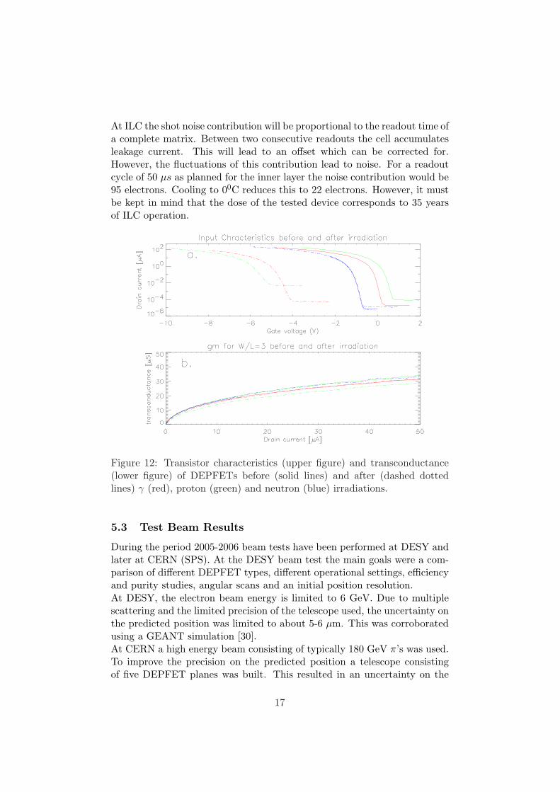
At ILC the shot noise contribution will be proportional to the readout time ofa complete matrix. Between two consecutive readouts the cell accumulatesleakage current. This will lead to an offset which can be corrected for.However, the fluctuations of this contribution lead to noise. For a readoutcycle of 50 µs as planned for the inner layer the noise contribution would be95 electrons. Cooling to 00C reduces this to 22 electrons. However, it mustbe kept in mind that the dose of the tested device corresponds to 35 yearsof ILC operation.
Figure 12: Transistor characteristics (upper figure) and transconductance(lower figure) of DEPFETs before (solid lines) and after (dashed dottedlines) γ (red), proton (green) and neutron (blue) irradiations.
5.3 Test Beam Results
During the period 2005-2006 beam tests have been performed at DESY andlater at CERN (SPS). At the DESY beam test the main goals were a com-parison of different DEPFET types, different operational settings, efficiencyand purity studies, angular scans and an initial position resolution.At DESY, the electron beam energy is limited to 6 GeV. Due to multiplescattering and the limited precision of the telescope used, the uncertainty onthe predicted position was limited to about 5-6 µm. This was corroboratedusing a GEANT simulation [30].At CERN a high energy beam consisting of typically 180 GeV π’s was used.To improve the precision on the predicted position a telescope consistingof five DEPFET planes was built. This resulted in an uncertainty on the
17

)σSeed cut (0 5 10 15 20 25 30 35 40
Eff
icie
ncy
(%
)
97.5
98
98.5
99
99.5
100
Standard efficiency
cut2χApplying modest
)σSeed cut (0 2 4 6 8 10 12 14 16 18 20
Pu
rity
(%
)
50
60
70
80
90
100
Figure 13: Efficiency (left) and purity (right) as a function of the seedcutfor a CCG-HE DEPFET.
predicted position of less than 1 µm and a single hit resolution better than2 µm at a DEPFET S/N>110. At CERN also the zero-suppression capa-bility of the CURO was tested, see section 5.3.4. The last CERN beam testwas finished on the 1st of November, hence the analysis of the CERN datais still in progress.
5.3.1 Device and Parameter Studies
DEPFET devices are available in different pixel sizes (Y×X): 22×36, 28.5×36and 24×36 µm2. In some DEPFET types, it was necessary to pulse theCLEAR GATE contact. This has as disadvantage that extra control linesare required. It is also possible to keep the CLEAR GATE contact at aconstant potential. This is referred to as a Common-Clear-gate (CCG) ma-trix. The improve the clear behavior, an extra high energy implant (HE)was implemented in some matrices. DEPFETs using the CCG-technologywith the HE implant display the same S/N (112.0±0.3 and 114.2±0.2)as a DEPFET without HE implant but with a clocked CLEAR GATE(112.7±0.2). DEPFETs with CCG-technology but without the HE implantperform worse, most likely due to extra noise by an incomplete clear.
5.3.2 Efficiency and Purity Studies
Efficiency
E =#clusters
#good tracks(2)
18

and purity
Purity =#good clusters
#all clusters=
#good clusters
#good + bad clusters(3)
is shown in Figure 13. The main result of the efficiency and purity measure-ment is that we can run with almost 100% purity and efficiency when usinga seed cut of ≈5-7σ. Note that this is a very low cut at only ≈5% of themost probable MIP signal.
5.3.3 Angular Scans
During one of the beam tests, the angle of incidence was varied. Rotationsaround both the X-axis (φ) and the Y-axis (θ) were made, between 0 and40o.At large angles, tracks traverse the silicon underneath many pixels. Hence,the signal per pixel is very low. This allows the study of charge generation inthin layers and the charge collection directly underneath the DEPFET pixelwhere the field lines are non-trivial. These studies are very important for thetuning of the GEANT simulation for the 50 µm thick DEPFETs foreseen forILC operation. The comparison is shown in figure 14. The correspondence isexcellent. The small difference at large angle is due to incomplete clusteringin the data. In the data it is demanded that the neighbors carry a signallarger than threshold. At large angle some clusters are therefore terminatedtoo early. These data provide a basis for the GEANT4 simulation of thinsensors (see section 6)
5.3.4 Zero-Suppression
In case that the background rates at the ILC are low, 0-suppression canbe used to reduce the data volume. Therefore, a 0-suppression capabilitywas implemented in the CURO. At CERN also the 0-suppression capabilitywas tested in a beam test. In figure 15 cluster signal distributions using alow, a medium and a high threshold are shown. The distributions follow theexpected behavior. For low thresholds some noise fluctuations are (falsely)identified as signal clusters. Furthermore, many neighbors are included inthe cluster. Both effects lead to a wide signal distribution with a tail tolower signals. When the threshold is increased, the background clustersare excluded, removing the tail on the lower signal side. At even higherthreshold, the signals on the neighbors are not included anymore in thecluster, leading to a narrow cluster signal distribution. The analysis is stillin progress. But the result demonstrates that the CURO can be read out0-suppressed.
19

Cluster size (pixel)0 5 10 15 20 25 30 35
En
trie
s
0
100
200
300
400
500
600
700
800
900 =0φ =10φ =20φ =30φ =40φ
Cluster size (pixel)0 5 10 15 20 25 30 35
En
trie
s
0
200
400
600
800
1000
1200
1400
1600
1800
2000
2200 =0φ =10φ =20φ =30φ =40φ
Cluster signal (ADC)1000 1500 2000 2500 3000 3500 4000
En
trie
s
0
50
100
150
200
250
300
350
=0φ =10φ =20φ =30φ =40φ
Cluster signal (ADC)1000 1500 2000 2500 3000 3500 4000
En
trie
s
0
20
40
60
80
100
120
140
160
180
=0φ =10φ =20φ =30φ =40φ
)oIncident Angle ( 0 5 10 15 20 25 30 35 40
Mo
st. P
rob
. Sig
nal
(A
DU
)
1900
2000
2100
2200
2300
2400
2500Data
Simulation
Figure 14: Comparison between data and GEANT simulation for the 450 µmDEPFET prototype. On the left cluster size and signal as a function of φ,on the right the corresponding simulation results. Also shown is the mostprobable signal as a function of the angle of incidence in both data andsimulation.
20

0 1000 2000 3000 4000 5000 6000 7000 80000
20
40
60
80
100
120
140
160
ClusterPH_noCuts
0 1000 2000 3000 4000 5000 6000 7000 80000
20
40
60
80
100
120
140
160
ClusterPH_noCuts
0 1000 2000 3000 4000 5000 6000 7000 80000
10
20
30
40
50
60
70
80
90
ClusterPH_noCuts
Figure 15: Cluster signals running the CURO with zero-suppression using alow (top), a medium (middle) and a high (bottom) threshold.
21

Resolution X (mm)-0.02 -0.015 -0.01 -0.005 0 0.005 0.01 0.015 0.02
En
trie
s
0
10
20
30
40
50
60
70m)µ 0.04 (±Resolution= 3.76
Resolution Y (mm)-0.02 -0.015 -0.01 -0.005 0 0.005 0.01 0.015 0.02
En
trie
s
0
20
40
60
80
100 m)µ 0.01 (±Resolution= 1.74
Figure 16: Residual width for a 36×22 µm (X×Y) DEPFET. The positionsare reconstructed using the η algorithm.
5.3.5 High Precision Resolution Studies using a DEPFET Tele-scope
At DESY the tracking was limited by the precision of the telescope andmultiple scattering. This telescope [26] has an intrinsic resolution of about4-5 µm. From the GEANT4 simulation [30], it was known that the DEPFETposition resolution was better than 2 µm. Optimally a telescope shouldhave an extraplolation precision in the DUT plane better than the intrinsicresolution of the DUT. To improve the precision of the tracking, a DEPFETbased telescope was developed and successfully operated.
Five DEPFETs were placed as close as possible to each other. Next tothe improved precision, this also has the advantage that much more dataon DEPFETs is collected. For the very high precision studies the middleDEPFET is used as DUT while the others are used as telescope planes. Oneedge DEPFET was also used for 0-suppression studies.
The hit positions are reconstructed using the η-algorithm. The residualdistributions are displayed in figure 16. The position resolutions are quitegood and still include a tracking and multiple scattering error. The resolu-tion in direction with smaller pitch (22 µm) is 1.74 µm. Of course, this isfor 450 µm thick sensors, the resolution of the 50 µm sensors will be worse(lower S/N, less charge sharing).
Using the software developed for [30], the uncertainty on the predictedposition was studied. In figure 17 the error on the predicted position for thismodule is plotted as a function of the observed residual width for variousbeam energies. The plot demonstrates that the error on the predicted posi-tion is approximately 0.77 µm! These results are still preliminary. There isstill room for improvement in the reconstructed position.
22

m)µObserved depfet resolution (0 0.5 1 1.5 2 2.5 3 3.5
m)
µE
rro
r o
n t
he
pre
dic
ted
po
siti
on
(
0
0.2
0.4
0.6
0.8
1
1.2
1.4
1.6
1.8
2
80 GeV
140 GeV
250 GeV
Figure 17: Error on the predicted position as a function of the observedresidual width for various beam energies.
6 Software Development
Simulation and reconstruction software is the key ingredient for the ILCDetector optimisation and performance studies. As the ILC communityentered the phase of intensive detector R&D, a need has arisen to havecoherent and consistent software tools allowing to perform
. Detailed GEANT4 based modeling of particle interactions with theILC detector.
. Realistic signal digitisation accounting for specific properties of read-out sensors in various sub-detectors.
. Full event reconstruction, including track finding, calorimeter cluster-ing, individual particle identification, jet reconstruction and calcula-tion of event shape variables.
Over recent years much effort has been invested to create a software stan-dard and data model for the ILC detector performance and physics studies.An example of software organization used in the study of the Large DetectorConcept (LDC) and Global Linear Collider Detector concept (GLD) is illus-trated in Figure 19. The detector simulation is performed with the GEANT4based program Mokka [27]. The package Marlin [28] facilitates implementa-tion of the signal digitisation procedure in various sub-detectors and differentsteps of event reconstruction in a modular way. The data flow is realizedvia the persistent LCIO (Linear Collider Input-Output) data model [29].
23

A detailed description of the DEPFET based vertex detector has beenimplemented as separate sub-detector driver within Mokka. The defaultlayout of the device is as described in section 4. The geometry relatedparameters, namely
. number of layers,
. number of ladders in each layer,
. geometrical parameters defining support frames, electronics, cablingetc,
. length, width and thickness of the active silicon wafers in each ladder,
are stored in a mySQL database and read in on-the-fly when running Mokka.By modifying the content of the database the impact of the vertex detectorgeometry on the performance of the device can be studied.
The default geometrical parameters used in the simulation are detailedin Table 2.
The simulation of particle interactions with the material of the micro-vertex detector has been complemented with the detailed DEPFET sensorresponse modeling, accounting for
. fluctuation of energy loss along the particle trajectory within the activelayer;
. diffusion of the released charge during its drift to the collection plane;
. Lorentz shift in the presence of the magnetic field;
. charge sharing across neighbouring pixels on the collection plane;
. electronic noise effects.
Simulation of the DEPFET sensor response is implemented as a separateMarlin module. Using the entry and exit points of a charged particle in theactive layer as input, the module produces an output in terms of a list offired pixels, characterized by their position within the wafers and inducedcharge. The simulation is controlled by steering parameters, including
. diffusion coefficient,
. factor converting energy lost into released charge,
. magnetic field,
. pixel dimensions,
. passive material.
24

The simulation code has been tuned and validated using DEPFET beamtest data taken at DESY in fall 2005. The 450 µm thick DEPFET matriceshave been exposed to a positron beam with an energy up to 6 GeV andtheir response have been studies as a function of particle incident angle.The parameters steering the simulation have been adjusted to ensure goodagreement of simulation and beam test data (see sect. 5.3.3).
The validated software is used to study the performance of the DEPFETbased ILC micro-vertex detector in terms of single point and impact param-eter resolutions. Figure 20 demonstrates the single point resolution in r−φand z as a function of the track polar angle for different thicknesses of theactive sensor and pixel size. The noise is assumed to be 100 electrons, thesilicon thickness to 50 µm corresponding to a S/N of 40:1 (for comparisonsimulations with 75 µm thick silicon were done as well). Dead material likethe reinforcement frames and ASIC chips and beam pipe is implemented.The r− φ impact parameter resolution as a function of particle momentumfor normally incident tracks and tracks at a polar angle of 45 degrees isshown in Figure 21. The r−φ impact parameter resolution is well describedby the relation
σ(IPr−φ) = a⊕ b
p · sin3/2 θ,
where p and θ are particle momentum and polar angle, respectively. The con-stant term is found to be a ∼ 4.5 µm independent of the active silicon waferthickness and a multiple scattering term b = 8.7(9.4) µm for the thickness ofactive silicon wafer of 50(75) µm. Thus, the DEPFET based vertex detectoris expected to meet ILC requirements (a < 5µm, b < 10µm·GeV) [1], pro-vided that pixel dimensions are smaller than 25x25 µm2 and the thickness ofthe sensitive layer is smaller than 75 µm. It is worthwhile mentioning thatthe thicker Silicon results in an improved point resolution due to a betterS/N. However, the impact parameter resolution gets slightly worse due tomultiple scattering.
The simulations were done assuming a 4T magnetic field. The depen-dence of the r − φ resolution on the field is shown in Figure 18 and variesfrom 3-4.3 µm for 3 - 5 T.
To enable large scale detector optimisation and physics studies, a stand-alone pattern recognition procedure in the micro-vertex detector has beendeveloped and integrated into the entire reconstruction chain within theMarlin framework. The stand-alone pattern recognition procedure in thevertex detector is applied to evaluate an impact of beam-induced back-grounds on the performance of the vertex detector.
At the ILC, the micro-vertex detector will operate in severe beam back-ground conditions. The primary source of the background is beamstrahlung,i.e. a radiation of photons of the colliding electron/positron in the electro-magnetic field of the opposite positron/electron bunch. The photons can in
25

Figure 18: r− φ resolution as function of the Lorentz angle. The values forB=3, 4 and 5 T are indicated
turn produce e+e− pairs or crash into forward detectors, creating secondaryparticles. Both e+e− pairs and secondary particles, backscattering from theforward region, may hit the vertex detector, thus contaminating the hit pat-tern produced by the physics events. Recent Monte Carlo studies showedthat in the innermost layers of the vertex detector one should expect severalhundred background hits per bunch crossing [3]. The total amount of accu-mulated background strongly depends on the readout speed which directlytranslates into an integrated number of bunch-crossings. Three scenarioshave been studied:
1. no background;
2. integration time of 25µs in the innermost layer and 50µs in the layers2−5, this corresponds to 75(150) integrated bunch crossings in thelayers 1(2−5); (optimistic)
3. integration time of 50µs in the innermost layer and 100µs in the layers2−5, this corresponds to 150(300) integrated bunch crossings in thelayers 1(2−5) (default).
For the nominal set of the ILC machine parameters the expected number ofbackground hits in the vertex detector is given in Table 5. The parameterssteering the pattern recognition procedure are optimized separately for eachof the three scenarios considered to minimize fake track rate while main-taining track finding efficiency at reasonably high level. Hence, the trackquality requirements get more stringent with deterioration of the backgroundconditions i.e. moving from scenario 1 to 3. The impact of beam-inducedbackgrounds on the pattern recognition performance is quantified using areference sample of the tt → 6 − jets at the centre of mass energy of 500
26

Figure 19: Organization of the simulation and reconstruction Software.
GeV. In scenarios 2 and 3, the hit patterns produced by physics events havebeen superimposed with the hit pattern expected from beam-induced back-grounds for a given detector integration time. Figure 22 shows the faketrack rate and the track finding efficiency as a function of the transversetrack momentum. Overall track finding efficiency and fake track rate foreach of the three scenarios considered are presented Table 6. The study em-phasizes the importance of having a device with high readout speed, whichwould allow to minimize effects of beam-induced background. It should benoted at this point that this is not DEPFET specific and applies to anytechnology employed for the ILC micro-vertex detector.
7 New Developments
7.1 PXD5 Pixel Production
A new production of DEPFET matrices, dubbed PXD5, started in 2006. Af-ter the proof of principle of the newly developed DEPFET technology andthe linearly shaped compact designs in the first detector production PXD4the first goal of PXD5 is to reproduce these features e.g. reliable transistoroperation, radiation hardness, internal amplification, selective access withinan array etc. In this sense PXD5 runs with an almost unchanged tech-nology focusing on more reliable processing. While the PXD4 wafer hostsdesigns for Xray and vertex detectors the PXD5 batch was split into waferscontaining either Xray or ILC designs both processed with almost the sametechnology. Thus the area of a full 150mm wafer is available for each project.For the ILC wafers a simpler and more robust backside processing was in-
27

Θcos 0 0.1 0.2 0.3 0.4 0.5 0.6 0.7 0.8 0.9 1
Po
int
Res
olu
tio
n, u
mφ
r-
0
1
2
3
4
5
6
7
82Thickness = 50 um, size=20x20um
2Thickness = 50 um, size=25x25um
2Thickness = 75 um, size=25x25um
Point Resolutionφr-
Θcos 0 0.1 0.2 0.3 0.4 0.5 0.6 0.7 0.8 0.9 1
Z P
oin
t R
eso
luti
on
, um
0
1
2
3
4
5
6
7
8
9
102Thickness=50um, size=20x20um
2Thickness=50um, size=25x25um
2Thickness=75um, size=25x25um
Z Point Resolution
Figure 20: The spatial point resolution in r−φ (left plot) and z (right plot)as a function of particle polar angle θ.
Particle Momentum, GeV0 2 4 6 8 10
Res
olu
tio
n, u
m
10
o=90trackθ
=20um L=50um, a=4.5um b=8.7umXS
=25um L=50um, a=4.6um b=8.7umXS
=25um L=75um, a=4.6um b=9.4umXS
D0 Resolution
Particle Momentum, GeV0 2 4 6 8 10
Res
olu
tio
n, u
m
10
o=45trackθ
=20um L=50umXS
=25um L=50umXS
=25um L=75umXS
D0 Resolution
Figure 21: The r − φ impact parameter resolution as a function of particlemomentum for the polar angles θ=90o (left plot) and θ=45o (right plot).
Layer background hits Background hits Background hitsper bunch crossing Scenario 2 Scenario 3
1 400 30000 600002 200 30000 600003 100 15000 300004 50 7500 150005 20 3000 6000
Table 5: The number of background hits per bunch crossing and the totalnumber of accumulated background hits in scenarios 2 and 3 (see text) forthe nominal set of the ILC machine parameters. The beam crossing angleis 14 mrad. The ILC detector includes the integrated dipole magnet. Thenumbers are taken from Reference [3].
28

Tp10
log-1 -0.5 0 0.5 1 1.5 2
Eff
icie
ncy
0
0.2
0.4
0.6
0.8
1
ttbar events
No background
75/150 bx
150/300 bx
TEfficiency vs p
θcos0 0.1 0.2 0.3 0.4 0.5 0.6 0.7 0.8 0.9 1
Eff
icie
ncy
0
0.2
0.4
0.6
0.8
1
θEfficiency vs
Tp10
log-1 -0.5 0 0.5 1 1.5 2
Fak
e tr
acks
/ ev
ent
-310
-210
-110
1
10
TFake track rate vs p
θcos0 0.1 0.2 0.3 0.4 0.5 0.6 0.7 0.8 0.9 1
Fak
e tr
acks
/ ev
ent
-310
-210
-110
1
10
θFake track rate vs
Figure 22: Track finding efficiencies (upper plots) and fake track rates as afunction of track transverse momentum (left plots) and polar angle (rightplots). Solid lines corresponds to a no background scenario, dashed lines tothe scenario characterized by an integration time of 75(150) µs and dottedline to the scenario characterized by an integration time of 150/300 µs (seetext).
Scenario Fakes per event Track finding efficiency, %pT > 0.1GeV pT > 0.5GeV
1 0.3 88 942 4.2 84 913 45 79 86
Table 6: The fake track rate and track finding efficiencies in the vertexdetector for the three scenarios of beam-induced backgrounds (see text).The reference physics process used is tt → 6− jets. In the case of scenarios2 and 3 hit patterns produced by physics events have been overlaid with hitpatterns expected from background for a given scenario.
29

troduced since there is no need for an ’ultra thin’ entrance window as it isnecessary for Xray detectors. The use of separate wafers also provides thespace for yield evaluations on larger pixel arrays.
7.1.1 Array and Pixel Sizes
The large 512 × 512 matrices address already the inner layer geometry of theILC vertex detector. Wide format detectors with 1024 readout channels ×256 switcher channels (array size = 16.38 × 12.29 mm2) are implemented tostudy the influence of long access lines (Gate, Clear) on the readout speed.For the other dimension very long arrays with 256 readout channels × 1024switcher channels (array size = 3.07 × 49.15 mm2) are designed to measurethe effect of the matrix input load on the readout chip. The pixel sizes varyfrom 32 ×24 µm2 (as in PXD4), over 24×24 µm2 (base line) to 20x20 µm2
(technology limit). An overview is given in table 7.
7.1.2 Internal Amplification and Clear Optimization
Electrons are drained into a highly n-doped Clear contact by applying ahigh positive voltage. Much desired is a complete Clear (no electrons leftin the internal gate) by which reset noise is totally canceled. The voltagedifference between Clear high and Clear off state is limited to 10V, whichis a requirement given by the new rad hard Switcher III (7.2). In principlethe Clear voltage can be significantly lowered by clocking the clear gatesimultaneously with clear contact. In this way the potential barrier betweenthe clear region and the internal gate is further reduced. However, thisoption leads to a less compact design and even worse implies a third controlline, switcher channel etc. Therefore for ILC the Clear gate is on a fixed(non clocked) potential common for the whole matrix - common Clear gatedesign. To find another way to facilitate the Clear process some wafers ofPXD4 contained a high energy phosphorous implantation. By this meansthe path of the removed electrons is shifted into the depth of the bulk andthe lateral fringing field gets larger. In the ’common Clear gate mode’complete Clear at voltages down to about 7V was measured on DEPFETsfabricated with this technology option (see PRC report 2005 [25]). However,the vertical position of internal gate is also deeper resulting in a 25% lowerinternal amplification (gq). In PXD5 the energy of the deep phosphorousimplantation is set to the same value applied for the internal gate formationthus the depth of the internal gate and hence the internal amplificationremain unchanged. According to simulations the Clear efficiency will beslightly worse than that of the high energy version but significantly improvedcompared to the standard technology.
Using the Clear gate in a passive way is another idea to improve the Clearbehavior. By increasing the coupling capacitance between the Clear contact
30

and the potentially floating Clear gate contact the latter one is pulled highduring each Clear process. The Clear gate off potential is connected rowwise via a high ohmic resistor. Various test structures and matrices areimplemented on PXD5 to study the ’capacitive coupled Clear’ option.
Since the main noise contribution still comes from fast readout electron-ics an increase of the internal DEPFET amplification gq transforms directlyinto S/N. The DEPFET still offers a large scaling potential. As illustratedin Figure 23 gq can be easily doubled by reducing the channel length fromcurrently used 4.5 µm to 2 µm. This range will be investigated on teststructures and arrays. However a reliable production of devices of shortchannel DEPFETS will require plasma etching techniques which have stillto be installed at the HLL.
Figure 23: Dependence of the charge amplification gq on the gate length.♦: 2D TesCA simulation (50 µA drain current); + measurements with 50µA (lower) and 100 µA (upper) drain current.
7.1.3 Charge Collection
An eventual discrepancy between gq values measured on single DEPFETsand small arrays with a Fe55 source to that obtained on larger arrays in beamtests can be explained by charge losses in the latter arrays. The amplificationachieved in beam test where the averaged charge is considered is by 20-30 %lower than that derived from the spectra. Results of 3D device simulationsobtained in collaboration with Dr. K. Gartner from WIAS Berlin suggestthat there are charge losses in the Clear gate region due to very weak lateraldrift fields near the surface. The DEPFET current response to 1600 e−
generated at different bulk positions was simulated. Slow charge collectionand losses can be avoided by additional lateral drift fields and optimizeddoping profiles which were implemented in the PXD5 design.
31

type pixels readout switcher pixel size array sizechannels channels (µm)2 (mm)2
large matrix 512 × 512 1024 256 32 × 24 16.4 × 12.3long matrix 128 × 2048 256 1024 24 × 24 3 × 49standard 64 × 256 128 128 32 × 24 2.0 × 6.2
24 × 24 1.5 × 6.220 × 20 1.3 × 5.1
PXD4 standard 64 × 128 128 64 32 × 24 2.0 × 3.124× 24 1.5 × 3.1
Table 7: Matrix sizes of the PXD5 production. The standard and minimatrices will exist in several design variations. For backwards compatibilitystandard matrices as in PXD4, compatible with the old switcher and CUROexist as well.
7.1.4 Other Features
An ILC DEPFET array will be connected to the Switcher and readout chipsvia bump bonds. A test array for bump bonding is included.
Most of the test matrices are designed for the new Switcher III and a128x128 pixel layout. For backwards compatibility some smaller devices(128x64) will work with the old Switcher II chip on old hybrids.Better testability is obtained by new biassing schemes: This saves chipsallowing preselection of matrices by probing on the wafer.Furthermore various different pixel designs have to be compared in termsof reliable operation (yield), internal amplification, clear behavior, chargecollection efficiency.PXD5 will be produced on high resistivity 6” FZ wafers of 450 µm thickness.Production should be finished in Summer 2007.
7.2 The Switcher III Chip
The Switcher II can deliver high voltages (up to 30V) at the expense ofhigh power consumption. The HV-CMOS process used is know to be notradiation hard (Indeed, the device stops working after 30 krad). This choicewas needed for the early prototype matrices when especially clear voltagesneeded for a complete clear were not known exactly. Now it is confirmedthat maximally 10V are needed for a complete clear.Hence a new switcher chip (Switcher III) was developed with following fea-tures:
. Switch up to 10V very fast (4ns settling time).
. Radiation hard design (0.35 µm).
. Ready for bump bonding.
32

Figure 24: Large matrix with 512 × 512 pixels. The sensitive area of thearray measures 16.38 × 12.29 mm2
. 128 channels (less chips needed).
. Reduced chip area (1.24 × 5.8 mm2)
. Reduced number of control signals.
. Flexible sequences instead of the simple row-by-row logic. This offersthe possibility for an ROI readout.
. Low power consumption.
The switching voltages of 10 V is achieved by staggering 3 transistors,each switching maximally 3.3 V [23]. The chip will fit well on the reinforce-ment frame of the DEPFET sensor.
Test chips have been submitted and functionality and radiation hard-ness (up to 600 krad)has already been demonstrated [23]. A production ofcomplete chips has been submitted.
7.3 The DCD1 Readout Chip
A new readout chip DCD1 (Drain Current Digitizer) has been developedwhich will overcome some shortcomings of the CURO:
. The CURO chip was designed for small matrices with low capacitance.In order to operate full size matrices the regulated cascode has to
33

be optimized for larger capacitances (about 40-50 pF for 5 cm longcolumns). From simulations a noise of 34 nA at 50pF is expected.
. An 8 bit, 16 MHz ADC will be added to each channel.
. Data is send out without 0-suppression. In test systems 0-suppressioncan be emulated using a FPGA. This will give a higher flexibilitytesting different 0-suppression and clustering algorithms. In case ofvery high occupancy 0-suppression is less attractive anyway.
. Power consumption should be 5 mW per channel.
. Improved timing.
. The chip will be prepared for bump bonding, wire bonding is possibleusing adaptor cards.
The chip will be made in a potentially rad hard UMC 0.18 µm technologyand will read 144 channels. The connection to the DEPFET is done using an18 × 8 array for bump bonding. The width of the chip is only 1.5 mm, muchsmaller than the 1.8 mm required for 144 lines of 12.5 µm pitch. Hence allchips servicing a DEPFET can be arranged in one row without staggering.A small 72 channel test chip has been submitted in March 2007.
The new ASICs require new hardware (hybrids) for building test systemswhich are presently being designed in Bonn. Furthermore a multichannelprogrammable power supply is developed simplifying considerably the setupsused in the lab and test beams.
7.4 Bump Bonding Studies
For all test systems made so far the electrical connections between sensor andelectronics were made by wire bonds. However, in a compact, low materialILC module the use of bump bonding is mandatory. Therefore we want toemploy a bump bond technology which
. can be used for low volume production of test systems in the lab,
. is suitable for single chip bonding,
. can be extended towards industrial high volume production.
Mannheim started to study flip chip bonding with gold stud bumps con-nected with solder paste or conductive glue. The procedure is:
. Formation of a gold ball (free air ball) from a gold wire.
. Placement of the gold ball onto a the bondpad using ultrasonic bond-ing.
34

. The wire is ripped off.
. Glue or solder is applied.
. Flip chip bonding applying pressure and temperature.
Using a manual bonder first tests were made forming balls of 50 µm diameterfrom a 17.5 µm gold wire. These give studs of 60 µm diameter fitting on 80µm bond pads. The bond pitch can be 100 µm. The yield obtained with a 64bonds test device was 100%. The contact resistance was below 1 Ohm and avery good mechanical connection could be obtained. The next steps will bean optimization of the procedure in order to obtain lower bond forces andtemperatures. The manual bonder will be modified to allow semiautomaticplacement of the bumps. A test chip with 160 will be made. In orderto transfer this procedure quickly to the DEPFETs the next generation ofASICS (Switcher III and DCD1) is already equipped with bump bondingpads. The PXD5 production has a number of test matrices prepared forbump bonding.
8 Summary and Outlook
We believe that most R&D goals expressed in the PRC 2005 have been met:
. The thinning technology has been demonstrated
. Single DEPFET pixels have a low intrinsic noise of 40 electrons at abandwidth of 50 MHz.
. The radiation tolerance of the sensors up to 1 Mrad has been demon-strated. This is well above the requirement of at most 200 krad forILC
. Prototype readout and steering chips are close to ILC specificationsImproved version have been designed and submitted. These secondgeneration chips should be sufficiently radiation hard and show signif-icant improvements of system noise and readout speed.
. A prototype module and system demonstrator with 64 × 128 pixelsincluding all system components has been built and has been operatedsuccessfully in a test beam.
. In the CERN test beam a five plane telescope made using DEPFETdetectors was successfully operated. Preliminary results show that theerror on the extrapolated position in the DUT is smaller than 0.8 µm.
. Simulation studies started and demonstrated that a DEPFET vertexdetector as proposed fulfills ILC requirements.
. The technology to make low mass modules (≈0.1%X0) has been es-tablished.
35

. The estimated power consumption of a full five layer detector is lowenough (6.4W) that it can be cooled by air flow. Hence the materialbudget can be kept very low.
. New collaborators from Aachen, Karlsruhe, Prague and Valencia havebeen found.
. Members of the DEPFET collaboration (Bonn, Mannheim, MPI) joinedthe EUDET JRA1 activity, which will provide a precision telescope forILC detector (especially vertex detector) development. The experiencefrom the DEPFET testbeam system is an input to the design of theEUDET system. Furthermore DEPFET matrices will be used for theevaluation of the EUDET telescope.
Simulation studies need to be continued. Especially the large fake ratesat large |z| need studies. Alternative geometries like forward discs insteadof the long barrel geometry should be studied. The impact of a combinedtracking with external tracking detectors needs to be studied, too.Studies of EMI (electromagnetic interference) need to be done as soon as afacility becomes available.Special effort should go in the understanding of the limitations of noise andreadout speed experienced with the CURO chip. A second generation chiphas been designed (DCD1) which should show significant improvements.Another strategy to decrease system noise is to increase the internal gain ofthe DEPFET. By minimizing the gate length the gq can be increased. Sincegq determines the first amplification step secondary noise sources, which aredominant at present, become less important. The next pixel production hastest matrices with reduced gate length and increased gq. We are confidentthat we will be able to go to the next step of a system closer to ILC specswith respect to size (close to full size module), thickness and readout speed.
9 Acknowledgements
This work is supported by the German Ministerium fur Bildung, Wissenschaft,Forschung und Technologie (BMBF) under contracts no. 05HS6VK1, no. 05HS6VM1and no. 05HS6PD1,by the Humboldt Foundation,by the Spanish Ministry of Science and Education, project FPA2005-02935,by the Czech Science Foundation, project Nr. 202/07/0740.We would like to thank Devis Contarato (LBNL), Marco Battaglia (LBNLUC Berkeley) and Piero Giubilato (LBNL INFN Padova, Italy) for theirhelp with irradiations at LBNL.
36

References
[1] F. Richard, J.R. Schneider, D. Trines and A. Wagner, ”TESLA: Technical Design Report”, DESY 2001-01, ECFA 2001-209,TESLA Report 2001-023, TESLA-FEL 2001-05 (2001).
[2] G. Aarons et al., International Linear Collider Reference DesignReport, ILC-REPORT-2007-1, DESY-07-046 (April 2007)
[3] A. Vogel, Beam-Induced Backgrounds in the ILC Detector, talkpresented at the ECFA ILC Workshop, Valencia 09/11/2006
[4] J. Kemmer, G. Lutz, New semiconductor detector concepts, Nucl.Inst. & Meth. A253 356 (1987)
[5] J. Kemmer, G. Lutz et al., Experimental confirmation of a newsemiconductor detector principle, Nucl. Inst. & Meth. A288 92(1990)
[6] P. Klein et al., Study of a DEPJFET pixel matrix with continuousclear mechanism, Nucl. Inst. & Meth. A392 254 (1997)
[7] P. Fischer et al., First operation of a pixel imaging matrix basedon DEPFET pixels, Nucl. Inst. & Meth. A451 651 (2000)
[8] W. Neeser et al., The DEPFET Pixel BIOSCOPE, IEEE Trans.Nucl. Sci. 47 No.3 (2000).
[9] E. Gatti, P. Rehak, Semiconductor drift chamber - An applicationof a novel charge transport scheme, Nucl. Inst. & Meth. A225608 (1984)
[10] G. Cesura et al., New pixel detector concepts based on junctionfield effect transitors on high resistivity silicon, Nucl. Inst. &Meth. A377 521 (1996)
[11] M. Porro et al., Spectroscopic Performances of DePMOS De-tector/Amplifier Device with Respect to Different Filtering Tech-niques and Operating Conditions, IEEE Trans. Nucl. Sci. 53 No.1(2006).
[12] C. Sandow et al., Nucl. Inst. & Meth. A568 176 (2006)
[13] J. J. Velthuis et al., Nucl. Inst. & Meth. A569 57 (2006)
[14] L. Andricek et al., Nucl. Inst. & Meth. A565 165 (2006)
[15] M. Trimpl et al., Nucl. Inst. & Meth. A560 21 (2006)
37

[16] M. Trimpl, Design of a current based readout chip and developmentof a DEPFET pixel prototype system for the ILC vertex detector,PhD Thesis, University Bonn (2005)
[17] ISE TCAD Realease 7.0 V01.2b, DIOS 2001
[18] H. Gajewski et al., TESCA - Two Dimensional SemiconductorAnalysis Package, Handbuch, WIAS, Berlin, 1997
[19] T. Behnke, S. Bertolucci, R. D. Heuer and R. Settles, TESLA: Thesuperconducting electron positron linear collider with an integratedX-ray laser laboratory. Technical design report. Pt. 4: A detectorfor TESLA’, DESY-01-011.
[20] L. Andricek et al., Processing of ultra-thin silicon sensors forfuture e+e− linear collider experiments, IEEE Trans. Nucl. Sci.51 No. 3, pp. 1117–1120 (2004).
[21] W. Cooper, Fermilab, private communication
[22] C. Sandow: Ladungssammlung und Loschvorgang von DEPFETPixelsensoren, Diploma Thesis, Bonn University, (April 2005)
[23] P. Fischer et al., Progress towards a large area, thin DEPFETdetector module, Presentation at the vertex 2006 conference (Pe-rugia) by P. Fischer, submitted to NIM in December 2006
[24] P. Fischer et al.: DESY PRC report 4/2003
[25] P. Fischer et al.: DESY PRC report 4/2005
[26] J.Treis, P. Fischer, H. Kruger, L. Klingbeil, T. Lari, N. Wermes, Amodular pc based silicon microstrip beam telescope with high speeddata acquisition, Nucl. Inst. & Meth. A490 112 (2002)
[27] Mokka web page http://polywww.in2p3.fr/geant4/tesla/www/mokka/mokka.html
[28] F. Gaede, Nucl. Nucl. Inst. & Meth. A559 177 (2006)
[29] F. Gaede, T. Behnke, N. Graf, Tony Johnson, physics/0306114
[30] D. Scheirich,Testing Semiconductor Detectors Using Beam ofCharged Particles, Bachelor Thesis, Charles University Prague,Faculty of Mathematics and Physics, Prague, 2006.
38