deposition of amorphous carbon film using natural palm oil by bias assisted pyrolysis-cvd for solar
DESCRIPTION
http://www.as-se.org/IJPRES/paperInfo.aspx?ID=15499 In this paper, an in-situ boron doped amorphous carbon (a-C:B) film deposited by bias assisted pyrolysis-CVD using natural palm oil as carbon source was reported. The effects of negative bias on the optical band gap, resistivity as well as conductivity and electronic properties of a-C:B films have been explored by multiple analysis techniques such as UV-vis spectroscopy, current-voltage (I-V) measurement and solar simulator. We have observed negative bias -10 V and -20 V reduced the optical transparency and improved electrical properties of a-C:B films. The optical band gap decreased from 2.3eV (no applied bias) to 2.2eV (with DC bias). The current voltage measurement revealed a rectifying characteristic formed by a-C:B films and n-type silicon. Furthermore, the negative bias has improved the electronic properties of a-C:B film compared with 0 V bias. The open circuit voltage (VOC), current density (JSC), fill factor and efficienTRANSCRIPT

www.as‐se.org/ijpres International Journal of Power and Renewable Energy Systems Volume 1, 2014
12
Deposition of Amorphous Carbon Film Using Natural Palm Oil By Bias Assisted Pyrolysis‐CVD For Solar Cell Applications A. Ishak 1,3,*, K. Dayana 1, M. H. Mamat 1,2 , M. F. Malek 1, M. Rusop 1,2,**
1NANO‐ElecTronic Centre, Faculty of Electrical Engineering, Universiti Teknologi MARA, 40450 Shah Alam,
Selangor, Malaysia 2NANO‐SciTech Centre, Institute of Science, Universiti Teknologi MARA,
40450 Shah Alam, Selangor, Malaysia 3Facuty of Electrical Engineering,
UiTM Sarawak Kampus Kota Samarahan Jalan Meranek, Sarawak
*[email protected]; **[email protected]
Received 17 March 2014; Accepted 22 April 2014; Published 11 June 2014 © 2014 American Society of Science and Engineering Abstract
In this paper, an in‐situ boron doped amorphous carbon (a‐C:B) film deposited by bias assisted pyrolysis‐CVD using natural palm oil as carbon source was reported. The effects of negative bias on the optical band gap, resistivity as well as conductivity and electronic properties of a‐C:B films have been explored by multiple analysis techniques such as UV‐vis spectroscopy, current‐voltage (I‐V) measurement and solar simulator. We have observed negative bias ‐10 V and ‐20 V reduced the optical transparency and improved electrical properties of a‐C:B films. The optical band gap decreased from 2.3eV (no applied bias) to 2.2eV (with DC bias). The current voltage measurement revealed a rectifying characteristic formed by a‐C:B films and n‐type silicon. Furthermore, the negative bias has improved the electronic properties of a‐C:B film compared with 0 V bias. The open circuit voltage (VOC), current density (JSC), fill factor and efficiency at ‐20 V were 0.426V, 5.351mA/cm2, 0.243, and 0.553 %, respectively.
Keywords
Negative Bias; Pyrolysis‐CVD; Palm‐oil; Amorphous Carbon
Introduction
A fossil based carbon precursors were conventionally used for finding many variety of allotropes carbon [1‐3]. There has been some reports on the use of natural precursor such as turpentine oil, eucalyptus oil, and camphor powder to produce allotropes carbon by using chemical vapor deposition technique [1‐3]. Beside of those precursors, a palm oil the other natural source have been used as carbon source to synthesize a vertically aligned carbon nanotubes (CNT) by chemical vapor deposition technique [3]. The palm oil is scientifically known as hexaeconoic acid which was derived from fibrous exocorp and mesacarp of the fruits of palm tree. It has contained carbon (67), hydrogen (127) and oxygen (8) to form the chemical binding of C67H127O8 [3].
DC bias voltage either positive or negative can help for giving extra energy through bombarding effect [5, 6]. Among deposition parameters, negative bias applied to the substrates could significantly change film properties due to enhancement of adatom mobility and the effect of ion bombardment [4‐6]. It determines the kinetic bombardment energies of the ions arriving on the substrate and can significantly affect the chemical composition, structure and residual stresses in the as‐deposited films. The amorphous carbon (a‐C) deposited from many types of precursors and methods showed a good potential use in amorphous carbon solar cells [7‐9]. However, it was reported as a weakly p‐type in nature despite of very complex structure, high density of defect which restricted to dope efficiently and those factors were the main barrier for its application in various electronic devices [7‐9]. In order to solve that problem, the control of doping (boron) could reduce the existing of defect and at the same time modified the electronic properties [7‐9].
In fact, there have been reports [4‐6] about the influences of the substrate bias voltage on the structure and properties of carbon and as‐deposited metal oxide films. However, there is no many literatures reporting on the effect of DC negative bias on a‐C:B films from bio‐hydrocarbon palm oil precursor. Moreover, to the best of our knowledge,

International Journal of Power and Renewable Energy Systems Volume 1, 2014 www.as‐se.org/ijpres
13
there is no report on the use of its precursor for fabricated a‐C:B films on n‐type silicon (Au/a‐C:B/n‐Si/Au) using DC bias voltage. Instead of the advantage of the abundantly natural cheap resources of palm oil, the technique use is simple, fast, and relatively inexpensive method for synthesize a‐C:B films.
Experimental
The a‐C:B film was prepared by bias‐assisted pyrolysis‐CVD using the corning glass substrates (thickness: 1mm) and n‐Si (100) (thickness 325 + 25 µm, resistivity 1‐10 Ω cm). Substrates (glass and n‐silicon) were cleaned with acetone (C5H6O) followed by methanol (CH3OH) for 15 min in ultrasonic cleaner (power Sonic 405), respectively and the glass substrates were then rinse with deionizer water (DI) water for 15 min. Moreover, excess oxide layers of n‐type silicon substrates were continued by the etching process with diluted hydrofluoric acid (10%) solution for about 3 min before rinsing in DI water. Substrates were then blown with nitrogen gas. The cleaned of glass and silicon substrate was finally placed inside the furnace chamber as shown in Fig. 1.
The deposition temperature was set at 325oC for 1h deposition. A liquid of palm oil precursor was heated in the bottle outside the chamber at around 150oC by using hot platter (Stuart CB162) as shown Fig. 1. The vaporized of palm oil was pressured into the furnace chamber using aquarium air pumps (model GA8000) (not shown in Fig. 1) where the flow rate of vaporized palm oil was controlled by adjustable valve. The amount of vaporized palm oil, carrier gas argon were set to be constant at 114 mL/min, 200 mL/min, respectively by using AALBORG flow meter. For doping process, approximately 1.5g of boron was placed on the aluminium foil above the metal plate heater in the chamber.
FIG. 1 A SCHEMATIC DIAGRAM OF BIAS ASSISTED PYROLYSIS‐CVD
FIG. 2 THE MEASUREMENT TECHNIQUE FOR HETEROJUNCTION SOLAR CELL (Au/a‐C:B/n‐Si/Au)

www.as‐se.org/ijpres International Journal of Power and Renewable Energy Systems Volume 1, 2014
14
In the measurement of solar cell device, both sides of silicon (buttom and top) are deposited with approximately 60nm and 12nm of gold, respectively. Another gold with thickness of 60 nm deposited at the top surface of 12 nm gold for confirming the point of probe is properly contacted on the gold metal contact. The light closure is attached at the top of the device as shown in Fig. 2 (dark color) to ensure light strike only the area of 2 cm2. To complete the whole circuit, the other probe is connected to the conductive metal holder. Surface profiler (Veeco Dektak 150), Current‐voltage measurement (I‐V), Solar simulator (Bukuh Keiki EP200), and JASCO UV‐VIS/NIR Spectrophotometer (V‐670 EX) are used to characterize the thickness, optical, electrical and electronic properties, respectively.
Result and Discussion
A direct current bias voltage (DC) is varied from 0 V, ‐10 V, and ‐20 V, respectively to analyze the boron doped amorphous (a‐C:B) films. The substrate bias voltage can be directly related with ion energy using the following relation [10, 11]
pm
KVE b ; 1m0 ;
where k is a constant, Vb is the substrate bias voltage, P is the pressure and m is a coefficienct. Acording to this equation, the ion energy will be propertional to Vb when the flux of ions incident on the growing film isconstant. So the increasing Vb leads to the enhancement of adatom mobility and effects of ion bombardment resulting in the ion‐peening effect and subsequent re‐sputtering of the films [10, 11].
FIG. 3 THE FUNCTION OF APPLIED NEGATIVE DC BIAS VOLTAGE ON THE THICKNESS OF THIN FILM
The a‐C:B film thickness as a function of the applied DC bias is shown in Fig. 3 for a fixed deposition of time 1 h. Under the applied deposition conditions, the obtained a‐C:B films are homogenous in film thickness and composition over the entire silicon substrate. In the range of bias values going from 0 V towards ‐20 V, the thickness of a‐C:B films are slightly increases as negative DC bias increases. A maximum thickness of about 325 nm is obtained for substrate bias at ‐20 V while minimum thickness is about 150 nm for substrate bias at 0 V. The difference in film thickness as a function of applied bias can be related to the operating film growth and sub‐surface processes initiated by the incoming hydrcarbon and argon ions. At zero substrate bias voltage (0 V), only radicals, neutrals and electron will reach the growing film surface. Hence, a‐C:B film growth is determined by the physisorption, chemisorption and incorporation of the hydrocarbon growth precursor only. However, for a case of using low negative bias voltage (in this case ‐10 and ‐20 V), the impinging positive ions will increase the sticking of the radical growth precursosrs through the creation of dangling bonds. This might ultimately lead to enhanced film growth. It is reported that the optimum growth rate is about ‐200 V where ion energies larger than the threshold energy, the sputtering of bounded carbon atoms will negatively influence the overall growth rate of amorphous carbon thin film [6, 12, 13].
Fig. 4 shows the transmission spectra of a‐C:B films versus wavelength deposited at different applied DC bias voltage. It is found that the optical transmission has a high value (>90%) at the visible range 390 to 790 nm (1.56 to 3.18 eV), where those ranges contain the largest amount of energy based on solar spectra. The result shows a‐C:B deposited at

International Journal of Power and Renewable Energy Systems Volume 1, 2014 www.as‐se.org/ijpres
15
0 V is the highest while at ‐20 V is the lowest. The decrease of optical transmission spectrum with respect to the increasing of DC bias could be explained with the additional average thickness of a‐C:B films. The highest average thickness of a‐C:B film at ‐20 V (325 nm) indicates the lowest transmission spectrum while the lowest average thickness of a‐C:B film contributes to the highest transmission spectrum. The additional boron incorporated with a‐C films and reducing dangling bond by the increasing of DC bias might influence the structure of a‐C:B film. The increasing of sp2 phase in the film might reduce the transmission spectra as reported by [14]. However, we observe those ranges of DC negative bias, transmission spectra are slightly changed which suggest that DC bias at those ranges are suitable for maintaining the high transmission spectra. Han et al [15] discuss that having high transmittance (>85%) at visible range can suppress the reflection losses. High transmission is important in the application of solar cell, since the energy needs to be transmitted from one particle to another in films in order to obtain high efficiency.
FIG. 4 TRANSMISSION SPECTRA OF a‐C:B FILMS DEPOSITED WITH DIFFERENT BIAS VOLTAGE
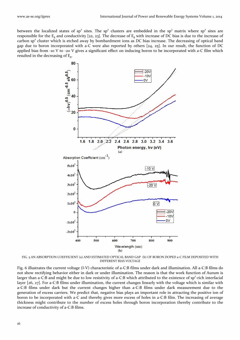
The absorption coefficient (α) indicates a measurement on the depth of light with a specific wavelength or energy penetrates into the film before being absorbed. It is calculated by the optical transmission of the film and the average film thickness. The absorption coefficient of a‐C:B films is calculated by Lambert’s Law α= 1/t (ln (1/T)) , where t is the thickness in nanometer (nm) and T is the transmission of the film. Fig. 5 (a) shows the variation of the absorption coefficient as a function of photon energy. As indicated from Fig. 5 (b), absorption coefficients at low energy are higher compared to the high energy. The value of α is found below 1x10³ (~1x10²–5x102 cm‐1) but comparable with reported by others [9, 16, 17]. The quite similar range value of α has also been reported for a‐C deposited by surface wave microwave plasma CVD [17, 18] (α~102–105 cm‐1), ion beam sputtering (α~104–105 cm‐1) [17] and reactive sputtering of graphite target (α102–104 cm‐1) [19].
The estimated optical band gaps (Eg) for amorphous semiconductors were obtained by Tauc relationship as [20, 21] (αhv)1/2 = B(Eg‐hv) where α is the absorption coefficient, B is the Tauc parameter and hv is the photon energy. The intercept of the Tauc’s slope in the photon energy axis gives the estimated optical gap, Eg. The estimated optical band gap of a‐C:B from 0 V, ‐10 V, and ‐20 V is 2.2, 2.3, and 2.31, respectively. It should be noted here that the optical band gap for all the samples is near the optimum range for optical band gap value for solar cell, which is about 1.5 eV. The result shows estimated optical band gaps slightly decreases as DC bias increase from ‐10 V to ‐20 V. We speculated, the decreasing of estimated optical band gap might be due to the increasing of interstitial doping of boron (B) in carbon films through modifications of C‐B bonding configurations by rearranging B atoms. The increasing of thickness might influence the boron to be incorporated with a‐C. The negative bias attracts more negative ions boron on the surface of the substrate thus increase the average thickness a‐C:B films at ‐10 V and ‐20 V respectively compared without DC bias. It is known that the optical gap is influenced by the hybridization state of carbon atoms. The local band gaps of the sp3 and sp2 site create band‐edge fractuations, with the sp3 site acting as tunneling barriers
www.as‐se.org/ijpres International Journal of Power and Renewable Energy Systems Volume 1, 2014
16
between the localized states of sp2 sites. The sp2 clusters are embedded in the sp3 matrix where sp2 sites are responsible for the Eg and conductivity [22, 23]. The decrease of Eg with increase of DC bias is due to the increase of carbon sp2 cluster which is etched away by bombardment ions as DC bias increase. The decreasing of optical band gap due to boron incorporated with a‐C were also reported by others [24, 25]. In our result, the function of DC applied bias from ‐10 V to ‐20 V gives a significant effect on inducing boron to be incorporated with a‐C film which resulted in the decreasing of Eg.
(a)
(b)
FIG. 5 AN ABSORPTION COEFFICIENT (a) AND ESTIMATED OPTICAL BAND GAP (b) OF BORON DOPED a‐C FILM DEPOSITED WITH DIFFERENT BIAS VOLTAGE
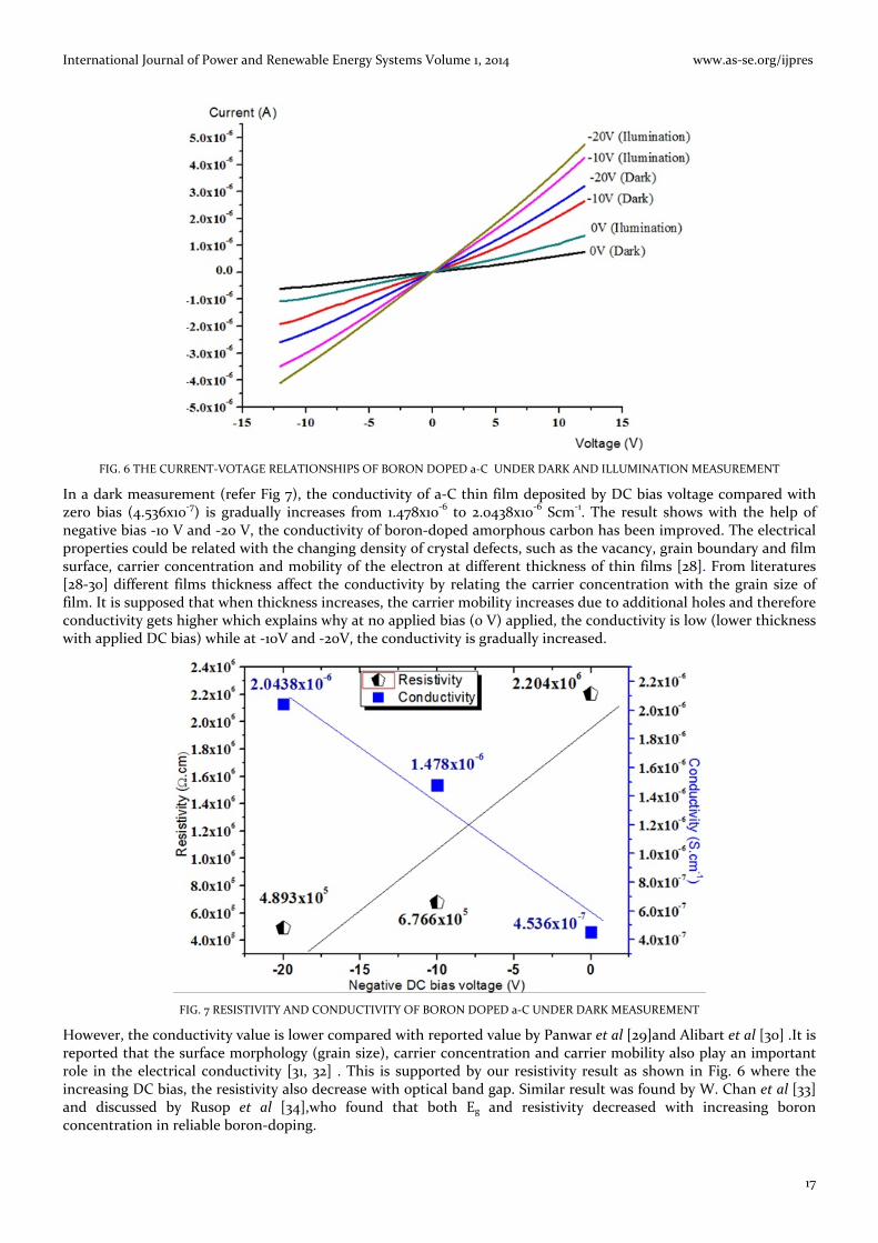
Fig. 6 illustrates the current voltage (I‐V) characteristic of a‐C:B films under dark and illumination. All a‐C:B films do not show rectifying behavior either in dark or under illumination. The reason is that the work function of Aurum is larger than a‐C:B and might be due to low resistivity of a‐C:B which attributed to the existence of sp2‐rich interfacial layer [26, 27]. For a‐C:B films under illumination, the current changes linearly with the voltage which is similar with a‐C:B films under dark but the current changes higher than a‐C:B films under dark measurement due to the generation of excess carriers. We predict that, negative bias plays an important role in attracting the positive ion of boron to be incorporated with a‐C and thereby gives more excess of holes in a‐C:B film. The increasing of average thickness might contribute to the number of excess holes through boron incorporation thereby contribute to the increase of conductivity of a‐C:B films.
International Journal of Power and Renewable Energy Systems Volume 1, 2014 www.as‐se.org/ijpres
17
FIG. 6 THE CURRENT‐VOTAGE RELATIONSHIPS OF BORON DOPED a‐C UNDER DARK AND ILLUMINATION MEASUREMENT
In a dark measurement (refer Fig 7), the conductivity of a‐C thin film deposited by DC bias voltage compared with zero bias (4.536x10‐7) is gradually increases from 1.478x10‐6 to 2.0438x10‐6 Scm‐1. The result shows with the help of negative bias ‐10 V and ‐20 V, the conductivity of boron‐doped amorphous carbon has been improved. The electrical properties could be related with the changing density of crystal defects, such as the vacancy, grain boundary and film surface, carrier concentration and mobility of the electron at different thickness of thin films [28]. From literatures [28‐30] different films thickness affect the conductivity by relating the carrier concentration with the grain size of film. It is supposed that when thickness increases, the carrier mobility increases due to additional holes and therefore conductivity gets higher which explains why at no applied bias (0 V) applied, the conductivity is low (lower thickness with applied DC bias) while at ‐10V and ‐20V, the conductivity is gradually increased.
FIG. 7 RESISTIVITY AND CONDUCTIVITY OF BORON DOPED a‐C UNDER DARK MEASUREMENT
However, the conductivity value is lower compared with reported value by Panwar et al [29]and Alibart et al [30] .It is reported that the surface morphology (grain size), carrier concentration and carrier mobility also play an important role in the electrical conductivity [31, 32] . This is supported by our resistivity result as shown in Fig. 6 where the increasing DC bias, the resistivity also decrease with optical band gap. Similar result was found by W. Chan et al [33] and discussed by Rusop et al [34],who found that both Eg and resistivity decreased with increasing boron concentration in reliable boron‐doping.

www.as‐se.org/ijpres International Journal of Power and Renewable Energy Systems Volume 1, 2014
18
TABLE 1 CONDUCTIVITY AND PHOTORESPONSE OF a‐C:B FILMS BY APPLIED DC
Applied DC bias voltage (V) Conductivity
(σ)photoresponse
Under dark Under illumination (σillumination/σdark)
0 4.536x10‐7 8.407x10
‐7 1.853
‐10 1.478x10‐6 2.746x10
‐6 1.857
‐20 2.0438x10‐7 3.126x10
‐6 1.531
Table 1 shows photo‐responses of a‐C:B films with a function of DC applied bias. Increment in conductivity values under illumination indicate photoresponse characteristic for thin films. Photoconductivity of thin films is important in addressing the suitability of thin films to be evaluated in photovoltaic solar cell applications. The photoresponse of a‐C:B film ranging from 0 V to ‐20 V is 1.853, 1.857, and 1.531, respectively. It observes that a‐C:B films have the overall range photoresponse below 2 with the highest one 1.857 at ‐10V. Although photoresponses are low, all a‐C:B films are obtained from new precursor palm oil which shows the ability to absorb light by producing current flow in the external circuit. Current flow is the results of the photoexcited carriers drift before recombination [35].
FIG. 8 THE CURRENT‐VOLTAGE CHRACTERISTICS UNDER DARK OF Au/a‐C:B/n‐Si/Au AT 0‐20 v
FIG. 9 THE CURRENT‐VOLTAGE CHARACTERISTICS UNDER ILLUMINATION OF Au/a‐C:B/n‐Si/Au SOLAR CELLS FABRICATED AT
DIFFERENT NEGATIVE BIAS

International Journal of Power and Renewable Energy Systems Volume 1, 2014 www.as‐se.org/ijpres
19
The current density voltage (J‐V) characteristics of Au/a‐C:B/n‐Si/Au solar cell under dark at 100 mW/cm2 using AM 1.5 solar simulator are shown in Fig. 9. It can be seen that Au/a‐C:B/n‐Si/Au displays rectifying curves under dark, indicating the formation of heterojunction between the a‐C:B film and silicon since Aurum (Au) metal contact is in the ohmic form with a‐C:B film as discussed previously. The a‐C:B layer acts as a p‐type in respect to silicon substrate to form the rectifying curve. It it clearly seen that, the reverse saturation current is low relative to the forward current, and gradually increases with reverse bias (photocurrent increases). We suppose, those behaviour might be due to the generation of minority carriers inside the depletion region. At forward bias, the current increases exponetially indicating a good quality of p‐n junction. The ideality factor is approximatelty 2 which means domination of recombination current rather than the diffusion current. Our results show, there are many deviation from the ideal p‐n characteristics which may be from the low doping efficiency. Furthermore, the absence of periodicity in a‐C makes the boron enter a chemically preferred 3‐fold coordinated site rather than the 4‐fold site which reflects to the small fraction of boron atoms enter 4‐fold sites[27].The same trend behaviour of heterojunction carbon solar cell is also demonstrated in literatures but using different methods and precursors [23, 27].
The current‐voltage characteristics of Au/a‐C:B/n‐Si/Au devices, under illumination are shown in Fig. 10 and their electronic properties are summarized in Fig. 11. The open circuit voltage (Voc), current density (JSC), fill factor (FF) and efficiency (%) of Au/a‐C:B/n‐Si/Au at 0V is approximately 0.055 V, 2.29 mA/cm2, 0.216, and 0.027 %, respectively. As DC bias applied at ‐10 V, the Voc, JSC, FF and η is 0.247 V, 2.451 mA/cm2, 0.236, and 0.143, respectively. Meanwhile, the VOC, JSC, FF and η of Au/a‐C:B/n‐Si/Au at DC bias ‐20 V is 0.426V, 5.351mA/cm2, 0.243, and 0.553%, respectively. It is shown that electronic properties of solar cell fabricated with applied DC bias have been improved notably through the increasing of DC bias substrate. It is observed, convension efficiency of Au/a‐C:B/n‐Si/Au solar cell deposited using low negative bias voltage of ‐20V is the highest as compared to ‐10 V and 0 V.The improvement of convension efficiency might be resulted from the number of boron incorporated with a‐C to contribute for the number of excess carriers in film. Although the energy conversion of solar cell device are considerably low but it shows the energy conversion efficiency using ‘green’ precursor is higher than reported by Tian et al (η=0.3 %)[27] and Hayashi et al (η =0.04 %) [23] when DC bias is applied.
FIG. 10THE SUMMARY OF ELECTRONIC PROPERTIES Au/a‐C:B/n‐Si/Au SOLAR CELL FARICATED AT 0 V, ‐10 V AND ‐20 V

www.as‐se.org/ijpres International Journal of Power and Renewable Energy Systems Volume 1, 2014
20
When light is incident on the surface of the solar cell device, photons with high energy will be strongly absorbed by the a‐C:B film, and excite excess carriers. In contrast, the photon with low energy will be mainly absorbed by the base region (Si). The shorter lifetime of excess carriers and diffusion length are responsible for the low photocurrent. Amorphous carbon consists of both π and σ bonds. The π state is more weakly bound as such easier to be broken [23, 27]. As a result, it forms high density of defects. In the meantime, boron doping will induce high‐concentration boron defect. The combination of defects from both of them will introduce deep states in the gap which can reduce minority carriers and diffusion length and thereby contribute to the reduction of overall of the performance of solar cell device especially, the photocurrent density. On the other hand, there are some improvements in electronic properties under DC bias where Voc, JSC, FF and η increase as compared without DC bias. The solar cell device results show, defects from a‐C and boron doping are reduced when DC bias is applied.
Moreover, the losses of light energy inside an Au metal might influenced to the lower efficiency of solar cell. It is reported that almost 50% of incident of light is absorbed by the Au film of about 10‐15 nm thickness [36] [37]. We predict high recombination on the surface and inside, the a‐C:B film is partly responsible for the low energy conversion efficiency. As discussed above, boron doping induces high‐concentration boron defect, and causes further structural disorder, these factors increase the recombination rate of minority carriers. As such, a greater portion of the light generated electron‐hole pairs will combine at the surface and inside the a‐C:B film, only few of them reach at the depletion region, and therefore contribute to the low energy conversion.
A series and shunt resistances caused by Au/a‐C:B/n‐Si/Au solar cell become low in value of VOC . The series resistance comes from the arrangement of solar cell device such as between metal contact and surface a‐C:B, the resistance itself of metal contact, recombination current in the depletion region, and the resistance in neutral p‐region (weakly p‐type) [38]. The series resistance gives rise to a voltage drop and therefore prevents the full photovoltaic voltage across the external load and therefore reduces the VOC [23, 39]. Other than that, the internal resistance of material (shunt resistance) comes from the edges of the device and grain boundaries as reported, [23, 34] might be also influenced by a‐C:B films. A fraction of photo generated carries are diverted away from the external load in consequences deteriorated the JSC.
FIG. 11 SPECTRAL RESPONSE OF HETEROJUNCTION SOLAR CELL DEVICE (Au/a‐C:B/n‐Si/Au) BY DIFFERENT SUBSTRATE NEGATIVE BIAS
Fig. 11 shows spectral response of Au/a‐C:B/n‐Si/Au at 0 V, ‐10 V, and ‐20 V of negative bias voltage. The Au/a‐C:B/n‐Si/Au at ‐20V show the highest spectral response as compared with the Au/a‐C:B/n‐Si/Au at 0 V and ‐10 V. Spectral responses (0 V, ‐10 Vand ‐20 V) indicate two broad bands at the peak wavelength approximately 550nm and 900nm of wavelengths. It is reported that the wavelength above 700nm is negligible since the photocurrent is mostly generated due to the silicon substrate [27, 40]. In the region below 700nm, boron doped layers act as carbon photon absorber, and quantum efficiency has a peak in short wavelength region. The photo current peak at approximately 550 nm is the good agreement with the optical band gap measurement.

International Journal of Power and Renewable Energy Systems Volume 1, 2014 www.as‐se.org/ijpres
21
Conclusion
The boron doped amorphous carbon film was successfully prepared by bias assisted pyrolysis‐CVD technique using palm oil as a carbon precursor. Negative DC bias improved the optical and electrical properties of a‐C:B films. The optical band gap decreased from 2.3eV (no applied bias) to 2.2eV (with DC bias) due to successfully interstitial doping of boron (B) in carbon films through modifications of C‐B bonding configurations by rearranging B atoms which was supported by optical band gap and conductivity film results. The current voltage measurement of solar simulator revealed a diode formed due to different layer from boron doped amorphous carbon film and n‐type silicon. The DC bias increased the electronic properties of ‐10 V and ‐20 V, respectively where at ‐20 V is the highest efficiency. The device of Au/a‐C:B/n‐Si/Au exhibited the photovoltaic behavior under illumination. The open circuit voltage (Voc), current density (JSC), fill factor (FF) and efficiency (%) of Au/a‐C:B/n‐Si/Au at 0V were approximately 0.254V, 0.234mA/cm2, 0.241, and 0.0141%, respectively. Meanwhile, the open circuit voltage (VOC), current density (JSC), fill factor and efficiency of Au/a‐C:B/n‐Si/Au at ‐20V were 0.426V, 5.351mA/cm2, 0.243, and 0.553%, respectively. The conversion efficiency increased from 0.0141 % to 0.553 % as negative bias increase from 0 V to ‐20V. Although the conversion efficiency is considerably low, it shows a good prospect of improvement of energy conversion efficiency using ‘green’ precursor of palm oil by optimizing the deposition conditions. The results show that precursor palm oil and bias assisted pyrolysis‐CVD can be developed as an alternative materials and process for solar cell applications.
ACKNOWLEDGMENT
The authors thank to Ministry of Higher Education (MOHE) Malaysia, UiTM Kota Samarahan Sarawak for the scholarship, NANO‐ElecTronic Centre, Faculty of Electrical Engineering, Universiti Teknologi MARA, NANO‐SciTech Centre, Institute of Science, Universiti Teknologi MARA, and Research Management Institute (RMI) Universiti Teknologi MARA (UiTM) for the facilities.
REFERENCES
[1] S. Paul and S. Samdarshi, "A< i> green</i> precursor for carbon nanotube synthesis," New Carbon Materials, vol. 26, pp. 85‐
88, 2011.
[2] R. Kumar, R. S. Tiwari, and O. N. Srivastava, "Scalable synthesis of aligned carbon nanotubes bundles using green natural
precursor: neem oil," Nanoscale research letters, vol. 6, p. 92, 2011.
[3] A. Suriani, A. Azira, S. Nik, R. Md Nor, and M. Rusop, "Synthesis of vertically aligned carbon nanotubes using natural palm
oil as carbon precursor," Materials Letters, vol. 63, pp. 2704‐2706, 2009.
[4] A. Mallikarjuna Reddy, A. Sivasankar Reddy, and P. Sreedhara Reddy, "Effect of substrate bias voltage on the physical
properties of dc reactive magnetron sputtered NiO thin films," Materials Chemistry and Physics, vol. 125, pp. 434‐439, 2011.
[5] H. Zhang, Z. Zhang, J. Li, and S. Cai, "Effects of direct current bias voltages on supported bilayer lipid membranes on a glassy
carbon electrode," Electrochemistry communications, vol. 9, pp. 605‐609, 2007.
[6] J. G. Buijnsters, M. Camero, L. Vázquez, F. Agulló‐Rueda, C. Gómez‐Aleixandre, and J. Albella, "DC substrate bias effects on
the physical properties of hydrogenated amorphous carbon films grown by plasma‐assisted chemical vapour deposition,"
Vacuum, vol. 81, pp. 1412‐1415, 2007.
[7] M. Rusop, X. Tian, S. Mominuzzaman, T. Soga, T. Jimbo, and M. Umeno, "Photoelectrical properties of pulsed laser deposited
boron doped p‐carbon/n‐silicon and phosphorus doped n‐carbon/p‐silicon heterojunction solar cells," Solar Energy, vol. 78,
pp. 406‐415, 2005.
[8] M. Rusop, S. M. Mominuzzaman, T. Soga, T. Jimbo, and M. Umeno, "Characterization of phosphorus‐doped amorphous
carbon and construction of n‐carbon/p‐silicon heterojunction solar cells," Japanese Journal of Applied Physics, vol. 42, p.
2339, 2003.
[9] S. Adhikari, D. C. Ghimire, H. R. Aryal, S. Adhikary, H. Uchida, and M. Umeno, "Boron‐doped hydrogenated amorphous
carbon films grown by surface‐wave mode microwave plasma chemical vapor deposition," Diamond and related materials,
vol. 15, pp. 1909‐1912, 2006.
[10] X. Tang, F. Luo, F. Ou, W. Zhou, D. Zhu, and Z. Huang, "Effects of negative substrate bias voltage on the structure and

www.as‐se.org/ijpres International Journal of Power and Renewable Energy Systems Volume 1, 2014
22
properties of aluminum oxide films prepared by DC reactive magnetron sputtering," Applied Surface Science, 2012.
[11] A. Bubenzer, B. Dischler, G. Brandt, and P. Koidl, "rf‐plasma deposited amorphous hydrogenated hard carbon thin films:
Preparation, properties, and applications," Journal of applied physics, vol. 54, pp. 4590‐4595, 1983.
[12] M. Weiler, S. Sattel, T. Giessen, K. Jung, H. Ehrhardt, V. Veerasamy, et al., "Preparation and properties of highly tetrahedral
hydrogenated amorphous carbon," Physical Review B, vol. 53, p. 1594, 1996.
[13] Y. Yamashita, K. Katayose, H. Toyoda, and H. Sugai, "Ion‐induced radical production on surfaces during deposition of
hydrogenated amorphous carbon," Journal of applied physics, vol. 68, pp. 3735‐3737, 1990.
[14] K. Chakrabarti, R. Chakrabarti, K. Chattopadhyay, S. Chaudhuri, and A. Pal, "Nano‐diamond films produced from CVD of
camphor," Diamond and related materials, vol. 7, pp. 845‐852, 1998.
[15] K.‐S. Han, J.‐H. Shin, and H. Lee, "Enhanced transmittance of glass plates for solar cells using nano‐imprint lithography,"
Solar Energy Materials and Solar Cells, vol. 94, pp. 583‐587, 2010.
[16] M. Rusop, S. Adhikari, A. Omer, T. Soga, T. Jimbo, and M. Umeno, "Effects of methane gas flow rate on the optoelectrical
properties of nitrogenated carbon thin films grown by surface wave microwave plasma chemical vapor deposition," Diamond
and related materials, vol. 15, pp. 371‐377, 2006.
[17] K. M. Krishna, Y. Nukaya, T. Soga, T. Jimbo, and M. Umeno, "Solar cells based on carbon thin films," Solar energy materials
and solar cells, vol. 65, pp. 163‐170, 2001.
[18] M. Rusop, A. Omer, S. Adhikary, T. Soga, T. Jimbo, and M. Umeno, "Effect of methane gas on the properties of nitrogenated
amorphous carbon films grown by surface wave microwave plasma CVD," Journal of non‐crystalline solids, vol. 351, pp. 2562‐
2567, 2005.
[19] L. Shen, Y. Xu, F. Meng, F. Li, S. Ruan, and W. Chen, "Semitransparent polymer solar cells using V< sub> 2</sub> O< sub>
5</sub>/Ag/V< sub> 2</sub> O< sub> 5</sub> as transparent anodes," Organic Electronics, vol. 12, pp. 1223‐1226, 2011.
[20] D. Pradhan and M. Sharon, "Opto‐electrical properties of amorphous carbon thin film deposited from natural precursor
camphor," Applied surface science, vol. 253, pp. 7004‐7010, 2007.
[21] S. Adhikari, S. Adhikary, A. M. Omer, M. Rusop, H. Uchida, T. Soga, et al., "Optical and structural properties of amorphous
carbon thin films deposited by microwave surface‐wave plasma CVD," Diamond and related materials, vol. 15, pp. 188‐192,
2006.
[22] J. Robertson, "Properties of diamond‐like carbon," Surface and Coatings Technology, vol. 50, pp. 185‐203, 1992.
[23] Y. Hayashi, S. Ishikawa, T. Soga, M. Umeno, and T. Jimbo, "Photovoltaic characteristics of boron‐doped hydrogenated
amorphous carbon on n‐Si substrate prepared by rf plasma‐enhanced CVD using trimethylboron," Diamond and related
materials, vol. 12, pp. 687‐690, 2003.
[24] M. Rusop, T. Kinugawa, T. Soga, and T. Jimbo, "Effect of Boron Weight Percentages in the Target of Pulsed Laser Deposition
on the Preparation of Boron‐Doped Amorphous Carbon Films," Surface Review and Letters, vol. 12, pp. 27‐34, 2005.
[25] J. Podder, M. Rusop, T. Soga, and T. Jimbo, "Boron doped amorphous carbon thin films grown by rf PECVD under different
partial pressure," Diamond and related materials, vol. 14, pp. 1799‐1804, 2005.
[26] F. Clough, W. Milne, B. Kleinsorge, J. Robertson, G. Amaratunga, and B. Roy, "Tetrahedrally bonded amorphous carbon (ta‐C)
thin film transistors," Electronics Letters, vol. 32, pp. 498‐499, 1996.
[27] X. Tian, M. Rusop, Y. Hayashi, T. Soga, T. Jimbo, and M. Umeno, "A photovoltaic cell from p‐type boron‐doped amorphous
carbon film," Solar energy materials and solar cells, vol. 77, pp. 105‐112, 2003.
[28] L. Huang and L. Meng, "Effects of film thickness on microstructure and electrical properties of the pyrite films," Materials
Science and Engineering: B, vol. 137, pp. 310‐314, 2007.
[29] O. Panwar, M. A. Khan, B. Satyanarayana, and S. Kumar, "Properties of boron and phosphorous incorporated tetrahedral
amorphous carbon films grown using filtered cathodic vacuum arc process," Applied Surface Science, vol. 256, pp. 4383‐4390,
2010.

International Journal of Power and Renewable Energy Systems Volume 1, 2014 www.as‐se.org/ijpres
23
[30] F. Alibart, O. Durand Drouhin, M. Lejeune, M. Benlahsen, S. Rodil, and E. Camps, "Evolution of the opto‐electronic
properties of amorphous carbon films as a function of nitrogen incorporation," Diamond and Related Materials, vol. 17, pp.
925‐930, 2008.
[31] L. Kumari, V. Prasad, and S. Subramanyam, "Effect of iodine incorporation on the electrical properties of amorphous
conducting carbon films," Carbon, vol. 41, pp. 1841‐1846, 2003.
[32] D. Kamaruzaman, N. Ahmad, I. Annuar, and M. Rusop, "Semiconducting Properties of Nanostructured Amorphous Carbon
Thin Films Incorporated with Iodine by Thermal Chemical Vapor Deposition," Japanese Journal of Applied Physics, vol. 52, p.
11NL02, 2013.
[33] W. Chan, T. Allen, F. Gaspari, J. Szurmak, E. Sagnes, and S. Zukotynski, "Amorphous diamond‐like carbon films prepared by
DC saddle‐field glow‐discharge method: doping with boron and phosphorus," in MRS Proceedings, 1997.
[34] M. Rusop, X. Tian, T. Kinugawa, T. Soga, T. Jimbo, and M. Umeno, "Preparation and characterization of boron‐incorporated
amorphous carbon films from a natural source of camphoric carbon as a precursor material," Applied surface science, vol. 252,
pp. 1693‐1703, 2005.
[35] T. Suemasu, T. Saito, K. Toh, A. Okada, and M. A. Khan, "Photoresponse properties of BaSi< sub> 2</sub> epitaxial films
grown on the tunnel junction for high‐efficiency thin‐film solar cells," Thin solid films, vol. 519, pp. 8501‐8504, 2011.
[36] H. Yu, T. Kaneko, S. Yoshimura, Y. Suhng, S. Otani, and Y. Sasaki, "The spectro‐photovoltaic characteristics of a
carbonaceous film/n‐type silicon (C/n‐Si) photovoltaic cell," Applied physics letters, vol. 69, pp. 4078‐4080, 1996.
[37] H. Yu, T. Kaneko, S. Yoshimura, Y. Suhng, Y. Sasaki, and S. Otani, "The junction characteristics of carbonaceous film/n‐type
silicon (C/n‐Si) layer photovoltaic cell," Applied physics letters, vol. 69, pp. 3042‐3044, 1996.
[38] S. M. Sze, Semiconductor devices: physics and technology: John Wiley & Sons, 2008.
[39] Z. Ma and B. Liu, "Boron‐doped diamond‐like amorphous carbon as photovoltaic films in solar cell," Solar energy materials
and solar cells, vol. 69, pp. 339‐344, 2001.
[40] M. Rusop, T. Soga, and T. Jimbo, "Photoelectrical properties of p‐type and n‐type electrical conductivity amorphous carbon
thin films for application in economical carbon‐based solar cells," Surface Review and Letters, vol. 12, pp. 343‐350, 2005.