derivation of switching angles of the cascaded multilevel ... · multilevel voltage source inverter...
TRANSCRIPT
Derivation of Switching angleS of the caScaDeD Multilevel voltage Source inverter SubjecteD
to a new PulSe wiDth MoDulation ScheMe
Zainal Salam1 and junaidi aziz2
1Falcuty of Electrical Engineering, Universiti Teknologi Malaysia, 81310 UTM, Skudai, Johor Darul Takzim
2The University of Nottingham, United Kingdom,
Email: [email protected]
abstractA new modulation scheme for a five-level cascaded multilevel inverter is proposed. Unlike other schemes, the proposed method is based on the symmetric regular sampling unipolar PWM with a single carrier and multiple modulating signals. The paper will detail the method to obtain the switching angles of this PWM scheme. This algorithm is implemented using a low-cost fixed-point microcontroller on an experimental five-level cascaded inverter test rig. The results from the test rig are compared with MATLAB simulation for verification.
Keywords: Harmonics, MATLAB, Multilevel Inverter, PWM
1.0 introDuctionRecently there is a surge in interest in the research related
to multilevel inverters. The main impetus for this is the fact that electrical equipment and machineries have begun to demand for power converters in the range of several Megawatts to be connected to a medium voltage network (2.3-6.9kV) [1]. Typical applications are electric train locomotives, heavy-duty ac drives, conveyer belts, and unified power-flow controllers. However, power (semiconductor) switches with the suitable switching frequency at ratings above 5kV are rare. Furthermore the ones that are available are prohibitively expensive to develop large power conversion systems for the above-mentioned applications. It is therefore uneconomical to achieve the required inverter output voltage using the existing power switches.
One approach to solve this problem is to utilise the multilevel voltage source inverter (MVSI) structure. Multilevel inverter is an array of power semiconductor switches and capacitor voltage sources, which is switched in a manner that an output voltage of stepped waveform is generated. For the normal two-level voltage source inverter, the maximum voltage output level is determined by the voltage blocking capability of each power switch. In contrast, for MVSI, the stress on each switch can be reduced in proportional to the number of output voltage levels. Thus with MVSI, higher input DC link voltage can be utilised using lower rated power switches. For example in high speed train locomotives which has DC link voltage of typically 2.5-3.5kV, standard IGBT switches rated at 1.8-2.4kV could be used in the five-level MVSI arrangement. In comparison, the 4.5kV and above IGCT used in single level inverter would be a much more expensive proposition.
Besides this important point, there are other advantages of the MVSI. It is possible to remove the expensive and bulky step-up transformer for applications that does not require galvanic isolation such as adjustable speed drives. Furthermore MVSI is known to improve harmonics performance, resulting in reduced switching losses. This is particularly crucial for high power application as increased power losses can complicate thermal management system design. With several levels in output waveform constructed using MVSI, the dV/dt on each power switch is reduced and so thus the EMI problem.
The development of MVSI began in the early 1980’s when Nabae et. al. [2] proposed the neutral-point clamped (NPC) pulse width modulation (PWM) inverter. Since then several multilevel topologies have evolved; most common are the NPC or Diode-Clamped Multilevel Inverter [2-4], Flying-Capacitor Multilevel Inverter [5] and Modular Structured Multilevel Inverter [6]. In addition there are emerging multilevel topologies such as the asymmetric hybrid cells [7] and soft-switching multilevel inverters [8]. To aid the reader in understanding some of the basic concepts of MVSI, a brief description of the three main MVSI topologies and the common modulation Pulse Width Modulation (PWM) techniques is given in the following paragraphs.
1.1 Diode-clamped Multilevel inverter (DcMi)
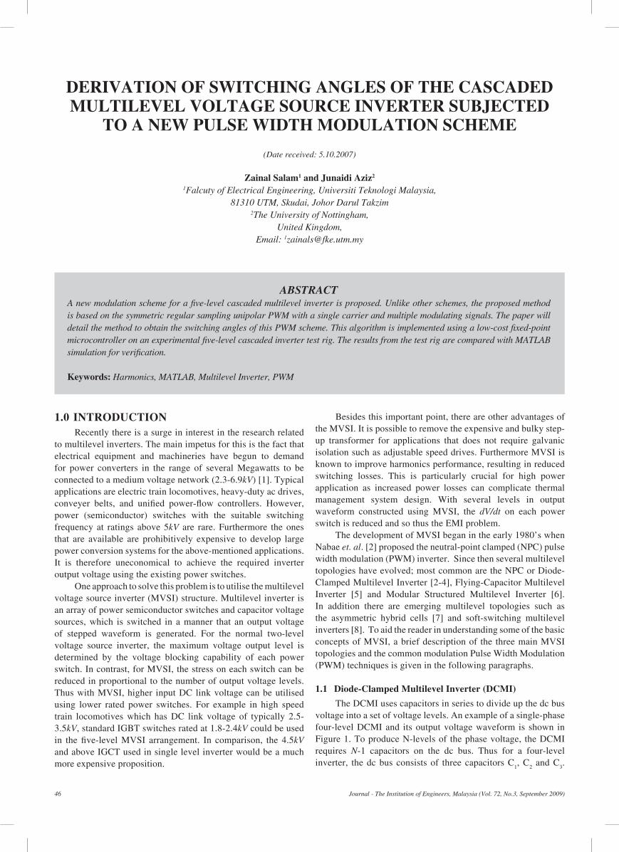
The DCMI uses capacitors in series to divide up the dc bus voltage into a set of voltage levels. An example of a single-phase four-level DCMI and its output voltage waveform is shown in Figure 1. To produce N-levels of the phase voltage, the DCMI requires N-1 capacitors on the dc bus. Thus for a four-level inverter, the dc bus consists of three capacitors C1, C2 and C3.
(Date received: 5.10.2007)
Journal - The Institution of Engineers, Malaysia (Vol. 72, No.3, September 2009)46
Derivation of Switching angleS of the caScaDeD Multilevel voltage Source inverter SubjecteD to a new PulSe wiDth MoDulation ScheMe
Journal - The Institution of Engineers, Malaysia (Vol. 72, No.3, September 2009) 47
For a dc bus voltage of Vdc, the voltage across each capacitor is Vdc/3. Consequently the voltage stress for each power device is limited to Vdc/3, through the clamping diodes.
Although each power switch only required to block a voltage level of Vdc/3, each clamping diodes need to have different voltage ratings for reverse voltage blocking. Assuming that each blocking diode voltage rating is the same as the power switches, the relationship between the diodes and the output voltage levels is expressed as (N-1)×(N-2)]. This represents a quadratic increase with respect to N, and for high level inverters, the system impractical to implement. Furthermore, the voltage unbalance problem across the capacitor make this topology is unattractive to handle real power flow control.
Figure 1(a): a single-phase four-level DcMI (b): Output voltage waveform
1.2 flying-capacitor Multilevel inverter (fcMi)
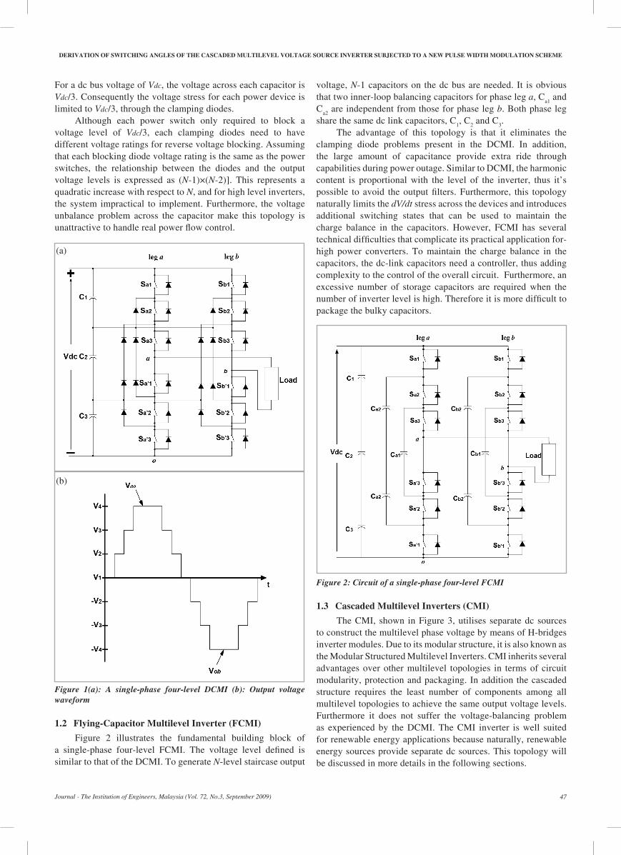
Figure 2 illustrates the fundamental building block of a single-phase four-level FCMI. The voltage level defined is similar to that of the DCMI. To generate N-level staircase output
voltage, N-1 capacitors on the dc bus are needed. It is obvious that two inner-loop balancing capacitors for phase leg a, Ca1 and Ca2 are independent from those for phase leg b. Both phase leg share the same dc link capacitors, C1, C2 and C3.
The advantage of this topology is that it eliminates the clamping diode problems present in the DCMI. In addition, the large amount of capacitance provide extra ride through capabilities during power outage. Similar to DCMI, the harmonic content is proportional with the level of the inverter, thus it’s possible to avoid the output filters. Furthermore, this topology naturally limits the dV/dt stress across the devices and introduces additional switching states that can be used to maintain the charge balance in the capacitors. However, FCMI has several technical difficulties that complicate its practical application for-high power converters. To maintain the charge balance in the capacitors, the dc-link capacitors need a controller, thus adding complexity to the control of the overall circuit. Furthermore, an excessive number of storage capacitors are required when the number of inverter level is high. Therefore it is more difficult to package the bulky capacitors.
Figure 2: circuit of a single-phase four-level FcMI
1.3 cascaded Multilevel inverters (cMi)
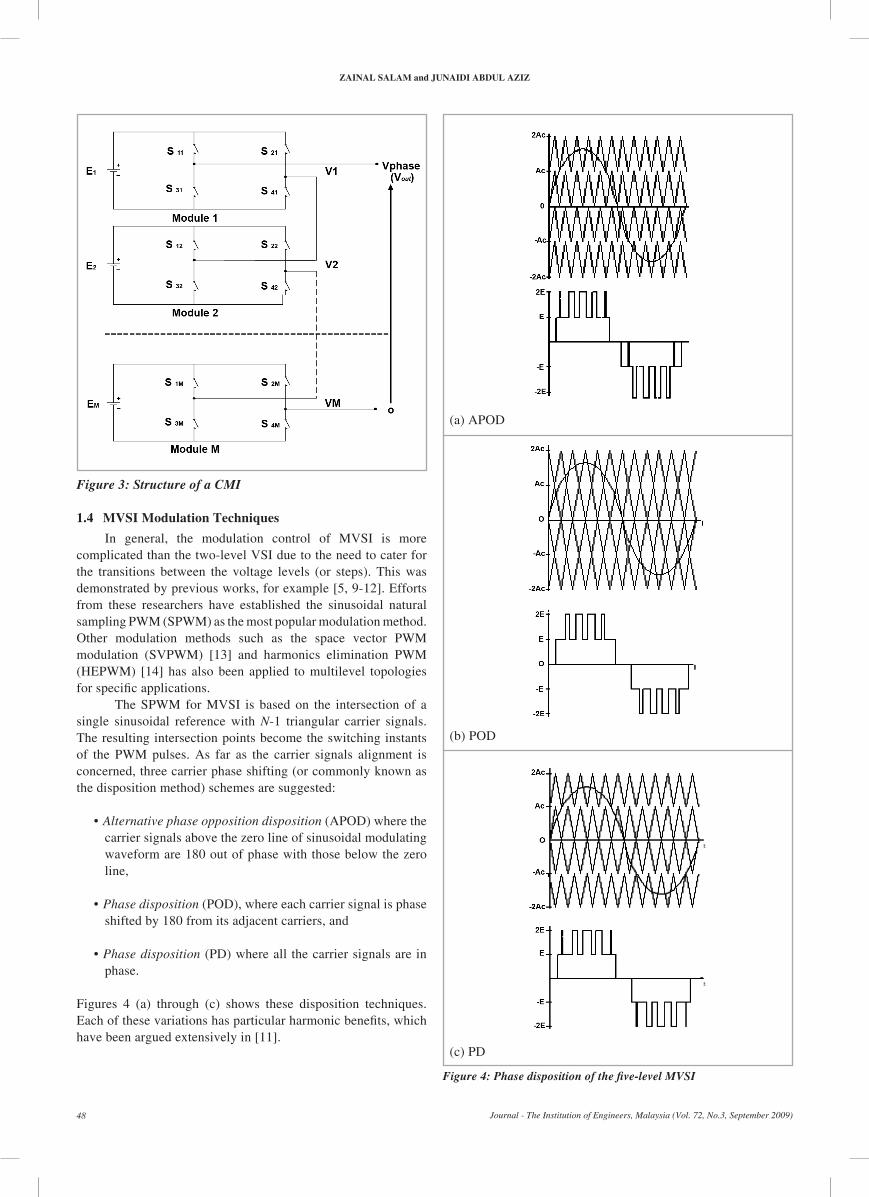
The CMI, shown in Figure 3, utilises separate dc sources to construct the multilevel phase voltage by means of H-bridges inverter modules. Due to its modular structure, it is also known as the Modular Structured Multilevel Inverters. CMI inherits several advantages over other multilevel topologies in terms of circuit modularity, protection and packaging. In addition the cascaded structure requires the least number of components among all multilevel topologies to achieve the same output voltage levels. Furthermore it does not suffer the voltage-balancing problem as experienced by the DCMI. The CMI inverter is well suited for renewable energy applications because naturally, renewable energy sources provide separate dc sources. This topology will be discussed in more details in the following sections.
(a)
(b)
Zainal SalaM and junaiDi abDul aZiZ
Journal - The Institution of Engineers, Malaysia (Vol. 72, No.3, September 2009)48
Figure 3: structure of a cMI
1.4 MvSi Modulation techniques
In general, the modulation control of MVSI is more complicated than the two-level VSI due to the need to cater for the transitions between the voltage levels (or steps). This was demonstrated by previous works, for example [5, 9-12]. Efforts from these researchers have established the sinusoidal natural sampling PWM (SPWM) as the most popular modulation method. Other modulation methods such as the space vector PWM modulation (SVPWM) [13] and harmonics elimination PWM (HEPWM) [14] has also been applied to multilevel topologies for specific applications.
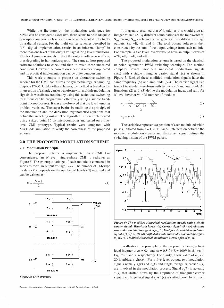
The SPWM for MVSI is based on the intersection of a single sinusoidal reference with N-1 triangular carrier signals. The resulting intersection points become the switching instants of the PWM pulses. As far as the carrier signals alignment is concerned, three carrier phase shifting (or commonly known as the disposition method) schemes are suggested:
• Alternative phase opposition disposition (APOD) where the carrier signals above the zero line of sinusoidal modulating waveform are 180 out of phase with those below the zero line,
• Phase disposition (POD), where each carrier signal is phase shifted by 180 from its adjacent carriers, and
• Phase disposition (PD) where all the carrier signals are in phase.
Figures 4 (a) through (c) shows these disposition techniques. Each of these variations has particular harmonic benefits, which have been argued extensively in [11].
(a) APOD
(b) POD
(c) PD
Figure 4: Phase disposition of the five-level MVSI
Derivation of Switching angleS of the caScaDeD Multilevel voltage Source inverter SubjecteD to a new PulSe wiDth MoDulation ScheMe
Journal - The Institution of Engineers, Malaysia (Vol. 72, No.3, September 2009) 49
While the literature on the modulation techniques for MVSI can be considered extensive, there seems to be inadequate description on how such scheme can be implemented effectively on a digital system. For the multi carrier schemes described in [16], digital implementation results in an inherent “jump” in more than one level of the output voltage during level transitions. The level jumps seriously distort the output voltage waveform, thus degrading its harmonics spectra. The same authors proposed software solutions to check and then to avoid these undesired conditions. However the correction scheme is rather complicated and its practical implementation can be quite cumbersome.
This work attempts to propose an alternative switching scheme for the CMI that utilizes the symmetric regular sampling unipolar PWM. Unlike other schemes, the method is based on the intersection of a single carrier waveform with multiple modulating signals. It was discovered that by using this technique, switching transitions can be programmed effectively using a simple fixed-point microprocessor. It was also observed that the level jumping problem vanished. The paper begins by outlining the principle of the modulation and the derivation trigonometric equations that define the switching instant. The algorithm is then implemented using a fixed point 16-bit microcontroller and tested on a five-level CMI prototype. Typical results were compared with MATLAB simulation to verify the correctness of the proposed scheme
2.0 the ProPoSeD MoDulation ScheMe 2.1 Modulation Principle
The proposed scheme is implemented on a CMI. For convenience, an N-level, single-phase CMI is redrawn as Figure 5. The ac output voltage of each module is connected in series to form an output voltage, Vout. The number of H-bridge module (M), depends on the number of levels (N) required and can be written as:
M = ——— (1)
Figure 5: cMI structure
It is usually assumed that N is odd, as this would give an integer-valued M. By different combinations of the four switches, S1M through S4M, each module can generate three different voltage outputs, i.e. +E, –E, and 0. The total output voltage is then constructed by the sum of the output voltage from each module. For example, a five level inverter would have an output levels of +2E, +E, 0, –E, and –2E.
The proposed modulation scheme is based on the classical unipolar, symmetric PWM switching technique. The method compares several modified sinusoidal modulation signals su(k) with a single triangular carrier signal c(k) as shown in Figure 5. Each of these modified modulation signals have the same frequency (fo) and amplitude (Am). The carrier signal is a train of triangular waveform with frequency fc and amplitude Ac. Equations (2) and (3) define the modulation index and ratio for N-level inverter with M number of modules:
m
i = ––– . –––––– = –––– (2)
––––––
mf = fc / fo (3)
The variable k represents a position of each modulated width pulses, initiated from k = 1, 2, 3… m
f /2. Intersection between the
modified modulation signals and the carrier signal defines the switching instant of the PWM pulses.
Figure 6: The modified sinusoidal modulation signals with a single carrier signal. Waveform labels: (a) carrier signal c(k), (b) absolute sinusoidal modulation signal m1 (t), (c) Modified sinusoidal modulation signal s1(k) of m1 (t), (d) shifted absolute sinusoidal modulation signal m2 (t), (e) Modified sinusoidal modulation signal s2(k) of m2 (t)
To illustrate the principle of the proposed scheme, a five-level inverter at m
i = 0.4 and mi = 0.8 for E = 100V is shown in
Figures 6 and 7, respectively. For clarity, a low value of mf, i.e.
20 is arbitrary chosen. For a five level output, two modulation signals namely s
1(k) and s
2(k) and single triangular carrier c(k)
are involved in the modulation process. Signal s2(k) is actually
s1(k) that shifted down by the amplitude of triangular carrier
signals Ac. In general signal s
u + 1(k) is shifted down by A
c from
N – 12
Am
Ac
Am
MAc
1(N – 1)
2
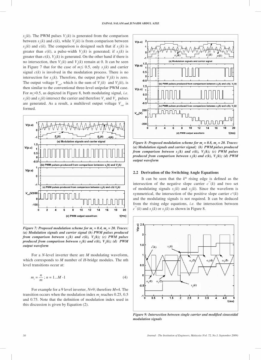
Zainal SalaM and junaiDi abDul aZiZ
Journal - The Institution of Engineers, Malaysia (Vol. 72, No.3, September 2009)50
nm
su(k). The PWM pulses V
1(k) is generated from the comparison
between s1(k) and c(k), while V
2(k) is from comparison between
s2(k) and c(k). The comparison is designed such that if s
1(k) is
greater than c(k), a pulse-width V1(k) is generated; if s
2(k) is
greater than c(k), V2(k) is generated. On the other hand if there is
no intersection, then V1(k) and V
2(k) remain at 0. It can be seen
in Figure 7 that for the case of mi≤ 0.5, only s
1(k) and carrier
signal c(k) is involved in the modulation process. There is no intersection for s
2(k). Therefore, the output pulse V
2(k) is zero.
The output voltage Vout
, which is the sum of V1(k) and V
2(k), is
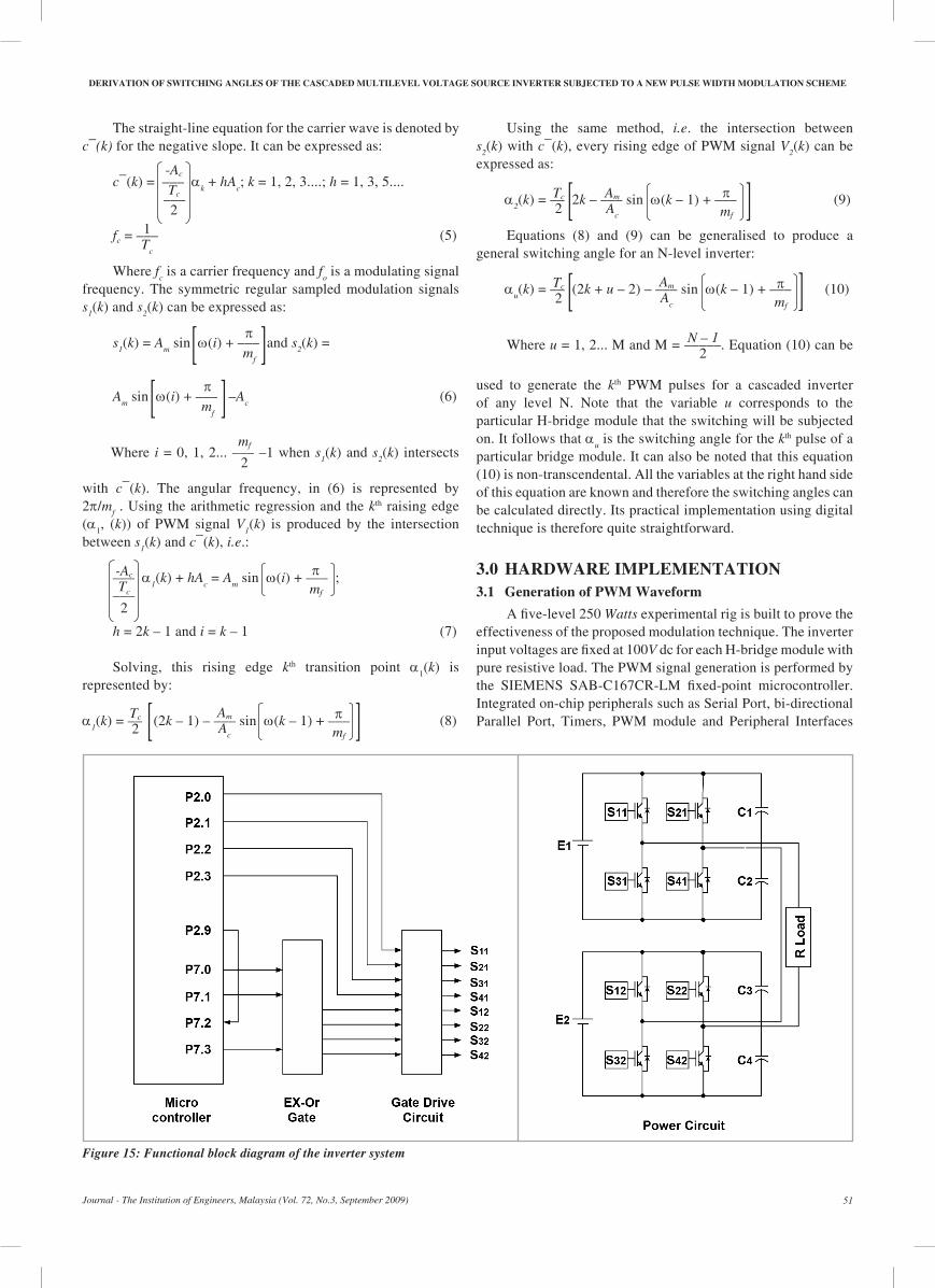
then similar to the conventional three-level unipolar PWM case. For m
i>0.5, as depicted in Figure 8, both modulating signal, i.e.
s1(k) and s
2(k) intersect the carrier and therefore V
1 and V
2 pulses
are generated. As a result, a multilevel output voltage Vout
is formed.
Figure 7: Proposed modulation scheme for mi = 0.4, mf = 20. traces: (a) Modulation signals and carrier signal (b) PWM pulses produced from comparison between s1(k) and c(k), V1(k); (c) PWM pulses produced from comparison between s2(k) and c(k), V2(k); (d) PWM output waveform
For a N-level inverter there are M modulating waveform, which corresponds to M number of H-bridge modules. The nth level transitions occur at:
m
i = –– ; n = 1...M -1 (4)
For example for a 9 level inverter, N=9; therefore M=4. The transition occurs when the modulation index m
i reaches 0.25, 0.5
and 0.75. Note that the definition of modulation index used in this discussion is given by Equation (2).
Figure 8: Proposed modulation scheme for mi = 0.8, mf = 20. traces: (a) Modulation signals and carrier signal; (b) PWM pulses produced from comparison between s1(k) and c(k), V1(k); (c) PWM pulses produced from comparison between s2(k) and c(k), V2(k); (d) PWM output waveform
2.2 Derivation of the Switching angle equations
It can be seen that the kth rising edge is defined as the intersection of the negative slope carrier c¯(k) and two set of modulating signals s1(k) and s2(k). Since the waveform is symmetrical, the intersection of the positive slope carrier c+(k) and the modulating signals is not required. It can be deduced from the rising edge equations, i.e. the intersection between c¯(k) and s
1(k) or s
2(k) as shown in Figure 8.
Figure 9: Intersection between single carrier and modified sinusoidal modulation signals
Derivation of Switching angleS of the caScaDeD Multilevel voltage Source inverter SubjecteD to a new PulSe wiDth MoDulation ScheMe
Journal - The Institution of Engineers, Malaysia (Vol. 72, No.3, September 2009) 51
mf
2
πmf
-Ac
Tc
2
πmf
Tc
2Am
Ac
The straight-line equation for the carrier wave is denoted by c¯(k) for the negative slope. It can be expressed as:
c¯(k) = ––– αk + hA
c; k = 1, 2, 3....; h = 1, 3, 5....
–––
fc = ––– (5)
Where fc is a carrier frequency and f
o is a modulating signal
frequency. The symmetric regular sampled modulation signals s
1(k) and s
2(k) can be expressed as:
s1(k) = A
m sin w(i) + ––– and s
2(k) =
Am sin w(i) + ––– –A
c (6)
Where i = 0, 1, 2... ––– –1 when s1(k) and s
2(k) intersects
with c¯(k). The angular frequency, in (6) is represented by 2π/m
f . Using the arithmetic regression and the kth raising edge
(α1, (k)) of PWM signal V1(k) is produced by the intersection
between s1(k) and c¯(k), i.e.:
––– α1(k) + hA
c = A
m sin w(i) + ––– ;
–––
h = 2k – 1 and i = k – 1 (7)
Solving, this rising edge kth transition point α1(k) is represented by:
α
1(k) = –– (2k – 1) – ––– sin w(k – 1) + ––– (8)
Using the same method, i.e. the intersection between s
2(k) with c¯(k), every rising edge of PWM signal V
2(k) can be
expressed as:
α2(k) = –– 2k – ––– sin w(k – 1) + ––– (9)
Equations (8) and (9) can be generalised to produce a general switching angle for an N-level inverter:
α
u(k) = –– (2k + u – 2) – ––– sin w(k – 1) + ––– (10)
Where u = 1, 2... M and M = –––––. Equation (10) can be used to generate the kth PWM pulses for a cascaded inverter of any level N. Note that the variable u corresponds to the particular H-bridge module that the switching will be subjected on. It follows that α
u is the switching angle for the kth pulse of a
particular bridge module. It can also be noted that this equation (10) is non-transcendental. All the variables at the right hand side of this equation are known and therefore the switching angles can be calculated directly. Its practical implementation using digital technique is therefore quite straightforward.
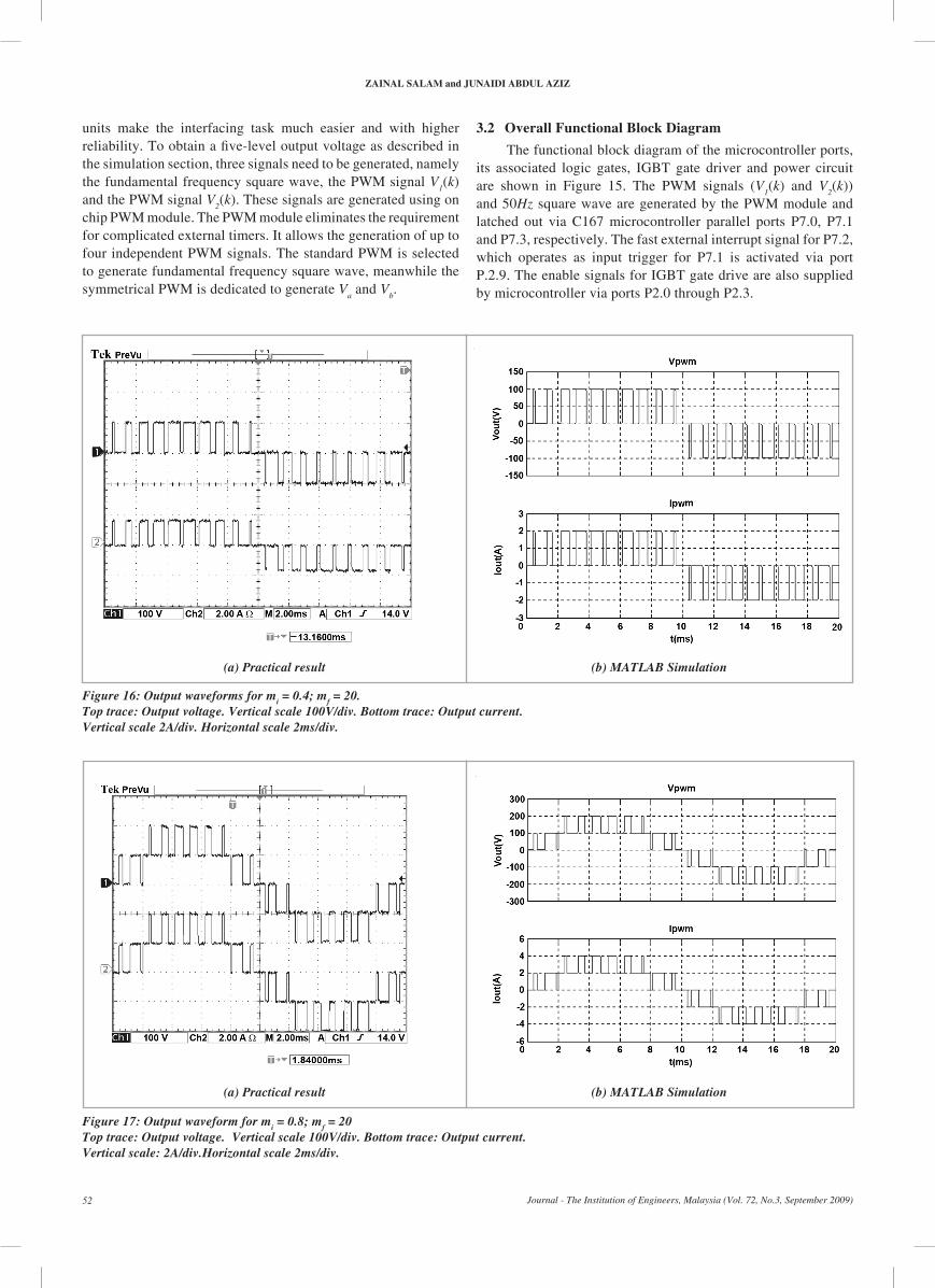
3.0 harDware iMPleMentation3.1 generation of PwM waveform
A five-level 250 Watts experimental rig is built to prove the effectiveness of the proposed modulation technique. The inverter input voltages are fixed at 100V dc for each H-bridge module with pure resistive load. The PWM signal generation is performed by the SIEMENS SAB-C167CR-LM fixed-point microcontroller. Integrated on-chip peripherals such as Serial Port, bi-directional Parallel Port, Timers, PWM module and Peripheral Interfaces
πm
f
πm
f
πmf
πmf
Tc
2
Tc
2
N – 12
Am
Ac
Am
Ac
Figure 15: Functional block diagram of the inverter system
-Ac
Tc
21T
c
Zainal SalaM and junaiDi abDul aZiZ
Journal - The Institution of Engineers, Malaysia (Vol. 72, No.3, September 2009)52
units make the interfacing task much easier and with higher reliability. To obtain a five-level output voltage as described in the simulation section, three signals need to be generated, namely the fundamental frequency square wave, the PWM signal V
1(k)
and the PWM signal V2(k). These signals are generated using on
chip PWM module. The PWM module eliminates the requirement for complicated external timers. It allows the generation of up to four independent PWM signals. The standard PWM is selected to generate fundamental frequency square wave, meanwhile the symmetrical PWM is dedicated to generate V
a and V
b.
3.2 overall functional block Diagram
The functional block diagram of the microcontroller ports, its associated logic gates, IGBT gate driver and power circuit are shown in Figure 15. The PWM signals (V
1(k) and V
2(k))
and 50Hz square wave are generated by the PWM module and latched out via C167 microcontroller parallel ports P7.0, P7.1 and P7.3, respectively. The fast external interrupt signal for P7.2, which operates as input trigger for P7.1 is activated via port P.2.9. The enable signals for IGBT gate drive are also supplied by microcontroller via ports P2.0 through P2.3.
(a) Practical result (b) MatLab simulation
(a) Practical result (b) MatLab simulation
Figure 16: Output waveforms for mi = 0.4; mf = 20. Top trace: Output voltage. Vertical scale 100V/div. Bottom trace: Output current. Vertical scale 2A/div. Horizontal scale 2ms/div.
Figure 17: Output waveform for mi = 0.8; mf = 20 Top trace: Output voltage. Vertical scale 100V/div. Bottom trace: Output current.Vertical scale: 2A/div.Horizontal scale 2ms/div.

Derivation of Switching angleS of the caScaDeD Multilevel voltage Source inverter SubjecteD to a new PulSe wiDth MoDulation ScheMe
Journal - The Institution of Engineers, Malaysia (Vol. 72, No.3, September 2009) 53
Figure 18: Harmonics of output voltage for mi = 0.4; mf = 20. Vertical scale 10V/div.Horizontal scale 500Hz/div
As illustrated in Figure 15, two modules of cascaded power circuit are required for a five-level inverter. Both modules are connected in series and constructed from IGBT switches and dc link capacitors. Power switches used for the inverter are type IRG430CKD IGBTs, manufactured by International Rectifier.
3.3 results
Figure 16 shows the oscillogram of the output voltage and current of the inverter for m
i = 0.4 and m
f = 20. For comparison,
MATLAB simulation results are shown side-by side. As can be
observed, the output voltage is similar to a three-level inverter, because m
i <0.5. For m
i = 0.8 and m
f = 20 shown in Figure 17,
the five-level PWM waveform is obtained. Clearly the output voltage is consistent with the theoretical prediction.
For the case of mf = 20 and m
i = 0.4, the output voltage
harmonic spectrum are shown in Figure 18, while for the case of m
f = 20; m
i = 0.8 it is illustrated in Figure 19. As can be
seen, the magnitude of the fundamental voltage for the latter case is doubled but the harmonics remain about the same. As a result, the ratio of its harmonics to a normalised fundamental is approximately half of the former.
(a) Practical
(a) Practical
(b) MatLab simulation
(b) MatLab simulation
Figure 19: Harmonics f output voltage for mi = 0.8; mf = 20. Horizontal scale 500Hz/div

Zainal SalaM and junaiDi abDul aZiZ
Journal - The Institution of Engineers, Malaysia (Vol. 72, No.3, September 2009)54
Figure 20 shows the comparison the harmonic profile of the proposed modulation technique with the POD scheme (using symmetrical regular sampling PWM). It can be observed that the proposed technique produces identical spectra to the POD scheme for all major harmonics. It can be suggested that both strategies produce harmonic components of the same magnitude and frequencies despite the obvious difference between the two modulation principles.
Figure 21 shows the comparison of the voltage THD between a five-level single-phase CMI and a conventional two-level inverter configuration. The figure shows that for both cases, a poor THD are obtained when the inverter operated at low modulation index. This is to be expected because at m
i ≤ 0.5, the cascaded
inverter essentially behaves like a conventional three-level inverter. A better THD is obtained when the inverter operated at higher modulation index, particularly when mi > 0.5. For example,
at modulation index equals 1.0, it was found that THD is three times superior compared to a conventional two-level inverter.
4.0 concluSionSThis paper presents a new switching scheme for the modular
structured multilevel inverter. The proposed scheme is based on symmetric regular sampled unipolar PWM, with multiple modulating waveforms and a single carrier. Mathematical equations that define the PWM switching instants are derived. Due to the non-transcendental nature of the equation, digital implementation is possible. A low power inverter test rig is built and the PWM algorithm is programmed using a low-cost fixed-point microcontroller. Several tests to quantify the performance of the inverter with the proposed modulation scheme are carried out. The results were compared with MATLAB simulation and are found to be in very close agreement.
Figure 20: comparison of harmonic spectrum between the proposed scheme and POD scheme
Figure 21: Variation of THD for five-level and two-level SPWM inverter configuration

Derivation of Switching angleS of the caScaDeD Multilevel voltage Source inverter SubjecteD to a new PulSe wiDth MoDulation ScheMe
Journal - The Institution of Engineers, Malaysia (Vol. 72, No.3, September 2009) 55
reference
[1] J.S. Lai, and F.Z. Feng, “Multilevel converters–A new breed of power converters”, IEEE Transaction on Industrial Applications, Vol IA-32, May/June 1996, pp.509-517.
[2] A. Nabae, I. Takahashi, H. Akagi, “A neutral -point clamped PWM inverter.” IEEE Transaction on Industrial Applications, vol. IA-17, Sep/Oct 1981, pp.518-523.
[3] T.A. Meynard, and H. Foch, “Multi-level Choppers for high voltage applications,” European Power Electronics and Drives Journal, Vol. 2, No. 1, March. 1992, pp.41-48.
[4] C. Hochgraf, R. Lasseter, D. Divan, and T.A. Lipo, “Comparison of multilevel inverters for static var compensation,” in Conf. Record of the IEEE-IAS Annual Meeting, IAS’ 94, pp.921–928.
[5] P. Hammond, “A new approach to enhance power quality for medium voltage ac drives,” IEEE Transaction on Industrial Applications, Vol IA-32, Vol. IA-33, Jan./Feb. 1997, pp. 202–208,
[6] E. Cengelci, S. U. Sulistijo, B. O. Woom, P. Enjeti, R. Teodorescu, and F. Blaabjerge, “A new medium voltage PWM inverter topology for adjustable speed drives,” in Conf. Record of the IEEE-IAS Annual Meeting, IAS’ 98, pp.1416–1423.
[7] M. D. Manjrekar, P. K. Steimer, and T. A. Lipo, “Hybrid multilevel power conversion system: a competitive solution for high-power applications,” IEEE Transaction on Industrial Applications, Vol. IA-36, May/June 2000, pp.834–841.
[8] X. Yuan and I. Barbi, “Zero voltage switching for three level capacitor clamping inverter,” IEEE Transaction on Power Electronics Vol. 14, July 1999, pp.771–781.
[9] L. Tolbert and T. G. Habetler, “Novel multilevel inverter carrier-based PWM method,” IEEE Transaction on Industrial Applications, Vol. IA-35, Sept./Oct. 1999, pp.1098–1107.
[10] Y. Liang and C. O. Nwankpa, “A new type of STATCOM Based on cascading voltage-source inverters with phase-shifted unipolar SPWM,” IEEE Transaction on Industrial Applications, Vol. IA-35, Sept/Oct. 1999, pp.1118–1123.
[11] B.P. McGrath and D.G. Holmes, “Multicarrier PWM Strategies for Multilevel Inverters.” IEEE Transaction on Industrial Electronics, Volume 49, Issue 4, Aug. 2002, pp.858 – 867.
[12] B.P. McGrath and D.G. Holmes, “An Analytical Technique for the Determination of Spectral Components of Multilevel Carrier-Based PWM Methods.” IEEE Transactions on Industrial Electronics, Vol. 49, Issue 4, Aug. 2002, pp.847 – 857
[13] N. Celanovic and D. Boroyevic, “A fast space vector modulation algorithm for multilevel three-phase converters,” in Conf. Record of the IEEE-IAS Annual Meeting IAS’99, pp.1173–1177.
[14] L. Li, D. Czarkowski, Y. Liu, and P. Pillay, “Multilevel selective harmonic elimination PWM technique in series-connected voltage inverters,” in Conf. Record of the IEEE-IAS Annual Meeting, IAS ’98, pp.1454–1461.
[15] Carrara G. et al., “A New Multilevel PWM Method; A Theoretical Analysis”, 21st Annual IEEE Power Electronics Specialist Conference, PESC ’90 pp.363-371.
[16] A. Dell’Aquila et al. “Novel Multilevel PWM Inverter Implementation”, 23rd International Conference on Industrial Electronics, Control and Instrumentation, IECON 97. Vol. 2, pp.710– 715.
ProfileS
Dr Zainal SalaMZainal Salam has been a lecturer at UTM for 23 years and is currently the Professor in Power Electronics at the Faculty of Electrical Engineering, UTM. He has been working in several researches and consulting works with SIRIM and GBT on battery powered converters. Currently he is the Director of the Inverter Quality Control Center (IQCC) UTM which is responsible to test PV inverters that are to be connected to the local utility grid. His research interests include all areas of power electronics, renewable energy, power electronics and machine control. Dr Zainal has written over 100 technical papers for various journals and conferences. He is currently working on high frequency inverters for PV applications.
junaiDi abDul aZiZJunaidi Abdul Aziz received the B.S and M Eng. degrees in electrical engineering from the Universiti Teknologi Malaysia in 2000 and 2002, respectively, and he received the Ph.D. degree in 2008 from the University of Nottingham. Since 2001, he has been with the Department of Energy Conversion at the Universiti Teknologi Malaysia, where he is presently a lecturer. His research interests include electric vehicle, ground power unit (GPU) and multilevel inverter.