desc: energy-efficient data exchange using synchronized counters
TRANSCRIPT

DESC: Energy-Efficient Data Exchange using
Synchronized Counters
Mahdi Nazm Bojnordi and Engin Ipek
University of Rochester
Rochester, NY 14627 USA
{bojnordi, ipek}@ece.rochester.edu
ABSTRACTIncreasing cache sizes in modern microprocessors requirelong wires to connect cache arrays to processor cores. Asa result, the last-level cache (LLC) has become a majorcontributor to processor energy, necessitating techniques toincrease the energy e�ciency of data exchange over LLCinterconnects.
This paper presents an energy-e�cient data exchange mech-anism using synchronized counters. The key idea is to rep-resent information by the delay between two consecutivepulses on a set of wires, which makes the number of statetransitions on the interconnect independent of the data pat-terns, and significantly lowers the activity factor. Simula-tion results show that the proposed technique reduces overallprocessor energy by 7%, and the L2 cache energy by 1.81⇥on a set of sixteen parallel applications. This e�ciency gainis attained at a cost of less than 1% area overhead to the L2cache, and a 2% delay overhead to execution time.
Categories and Subject DescriptorsB.3 [Hardware]: Memory Structures; B.4.3 [Hardware]:Input/Output and Data Communications—Interconnections
General TermsDesign, Management, Performance
KeywordsLow power, Interconnect, Caches, Data encoding, Signaling
1. INTRODUCTIONOn-chip interconnect is a major contributor to micropro-
cessor energy. Recent studies have shown that more than60% of the dynamic power in modern microprocessors is dis-sipated in driving on-chip interconnects [1, 2, 3]. Not onlydo long wires present a highly capacitive load, but they alsoexpend significant energy due to the repeaters inserted along
Permission to make digital or hard copies of all or part of this work for
personal or classroom use is granted without fee provided that copies are
not made or distributed for profit or commercial advantage and that copies
bear this notice and the full citation on the first page. To copy otherwise, to
republish, to post on servers or to redistribute to lists, requires prior specific
permission and/or a fee.
MICRO’46 December 7-11, 2013, Davis, CA, USA
Copyright 2013 ACM 978-1-4503-2561-5/13/12 ...$15.00.
the interconnect to linearize wire delay. Current scalingtrends indicate that interconnect power will be even higherin future billion-transistor multicore processors [4, 5].
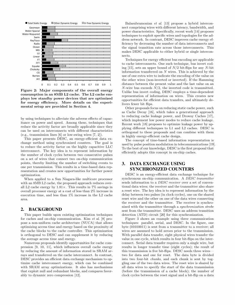
Last-level caches occupy significant area, and incur largeenergy and delay overheads in data exchange over long wires.Figure 1 shows the percentage of processor energy expendedon an 8MB cache when running a set of parallel applicationson a Sun Niagara-like multicore processor.1 On average, theL2 cache is responsible for 15% of the total processor en-ergy. Figure 2 breaks down the L2 cache energy into its con-stituent parts, and shows that communication over the long,capacitive H-tree interconnect is the dominant source of en-ergy consumption (80% on average) in the L2 cache. (Thisassumes that the L2 cache employs low standby power de-vices that are optimized for energy e�ciency, as explained inSection 4. L2 power would be even higher if high-speed—andthus, high leakage—transistors were used.) Consequently,numerous architectural techniques have been developed tomitigate interconnect energy in last-level caches.
0" 0.1" 0.2" 0.3" 0.4" 0.5" 0.6" 0.7" 0.8" 0.9" 1"
Art"Barnes"
CG"Cholesky"Equake"
FFT"FT"
Linear"LU"MG"
Ocean"Radix"
RayTrace"Swim"
WaterNNsquared"WaterNSpacial"
Geomean"
Figure 1: L2 energy as a fraction of total processorenergy. The processor configuration is explained inSection 4.
An e↵ective way of reducing cache interconnect energy isto reduce the activity factor—i.e., the switching probability—of the wires. This can be accomplished, for example, by en-coding the data such that successive transmissions on thedata bus flip the state of only a small number of wires, orby compressing the data in the last-level cache. Intercon-nect energy can also be reduced by reducing the voltage, or
1The experimental setup is explained in Section 4.
0" 0.1" 0.2" 0.3" 0.4" 0.5" 0.6" 0.7" 0.8" 0.9" 1"
Art"Barnes"
CG"Cholesky"Equake"
FFT"FT"
Linear"LU"MG"
Ocean"Radix"
RayTrace"Swim"
WaterNNsquared"WaterNSpacial"
Geomean"
Total"StaQc"Energy" Other"Dynamic"Energy" HNTree"Dynamic"Energy"
Figure 2: Major components of the overall energyconsumption in an 8MB L2 cache. The L2 cache em-ploys low standby power devices that are optimizedfor energy e�ciency. More details on the experi-mental setup are provided in Section 4.
by using techniques to alleviate the adverse e↵ects of capac-itance on power and speed. Among these, techniques thatreduce the activity factor are broadly applicable since theycan be used on interconnects with di↵erent characteristics(e.g., transmission lines [6] or low-swing wires [7, 2]).
This paper presents DESC, an energy-e�cient data ex-change method using synchronized counters. The goal isto reduce the activity factor on the highly capacitive LLCinterconnect. The key idea is to represent information bythe number of clock cycles between two consecutive pulseson a set of wires that connect two on-chip communicationpoints, thereby limiting the number of switching events toone per transmission. This results in a time-based data rep-resentation and creates new opportunities for further poweroptimization.
When applied to a Sun Niagara-like multicore processorwith an 8MB L2 cache, the proposed approach reduces over-all L2 cache energy by 1.81⇥. This results in 7% savings inoverall processor energy at a cost of less than 2% increase inexecution time, and less than 1% increase in the L2 cachearea.
2. BACKGROUNDThis paper builds upon existing optimization techniques
for caches and on-chip communication. Kim et al. [8] pro-pose a non-uniform cache architecture (NUCA) that allowsoptimizing access time and energy based on the proximity ofthe cache blocks to the cache controller. This optimizationis orthogonal to DESC and can supplement it by reducingthe average access time and energy.
Numerous proposals identify opportunities for cache com-pression [9, 10, 11], which influences overall cache energyby reducing the amount of information stored in SRAM ar-rays and transferred on the cache interconnect. In contrast,DESC provides an e�cient data exchange mechanism to op-timize cache interconnect energy, which can be combinedwith SRAM array optimizations. It also has mechanismsthat exploit null and redundant blocks, and compares favor-ably to dynamic zero compression [12].
Balasubramonian et al. [13] propose a hybrid intercon-nect comprising wires with di↵erent latency, bandwidth, andpower characteristics. Specifically, recent work [14] proposestechniques to exploit specific wires and topologies for the ad-dress network. In contrast, DESC improves cache energy ef-ficiency by decreasing the number of data interconnects andthe signal transition rate across those interconnects. Thismakes DESC applicable to either hybrid or single intercon-nects.
Techniques for energy e�cient bus encoding are applicableto cache interconnects. One such technique, bus invert cod-ing [15], sets an upper bound of N/2 bit-flips for any N -bitinformation transferred on N wires. This is achieved by theuse of one extra wire to indicate the encoding of the value onthe other wires (non-inverted or inverted). If the Hammingdistance between the present value and the last value on anN -wire bus exceeds N/2, the inverted code is transmitted.Unlike bus invert coding, DESC employs a time-dependentrepresentation of information on wires. This creates newopportunities for e�cient data transfers, and ultimately de-livers fewer bit flips.
Other proposals focus on reducing static cache power, suchas Cache Decay [16], which takes a generational approachto reducing cache leakage power, and Drowsy Caches [17],which implement low power modes to reduce cache leakage.Recent work [18] proposes to optimize leakage power by ap-plying di↵erent techniques to L1 and L2 caches. DESC isorthogonal to these proposals and can combine with themin highly energy-e�cient cache design.
The concept of time-based information representation isused by pulse position modulation in telecommunications [19].To the best of our knowledge, DESC is the first proposal thate�ciently adopts this concept in on-chip caches.
3. DATA EXCHANGE USINGSYNCHRONIZED COUNTERS
DESC is an energy-e�cient data exchange technique forsynchronous on-chip communication. A DESC transmitter
sends information to a DESC receiver over a set of conven-tional data wires; the receiver and the transmitter also sharea reset wire. The key idea is to represent information by thedelay between two pulses (in clock cycles), one on the sharedreset wire and the other on one of the data wires connectingthe receiver and the transmitter. The receiver is synchro-nized with the transmitter through a synchronization strobe
sent from the transmitter. DESC uses an address transitiondetection (ATD) circuit [20] for this synchronization.
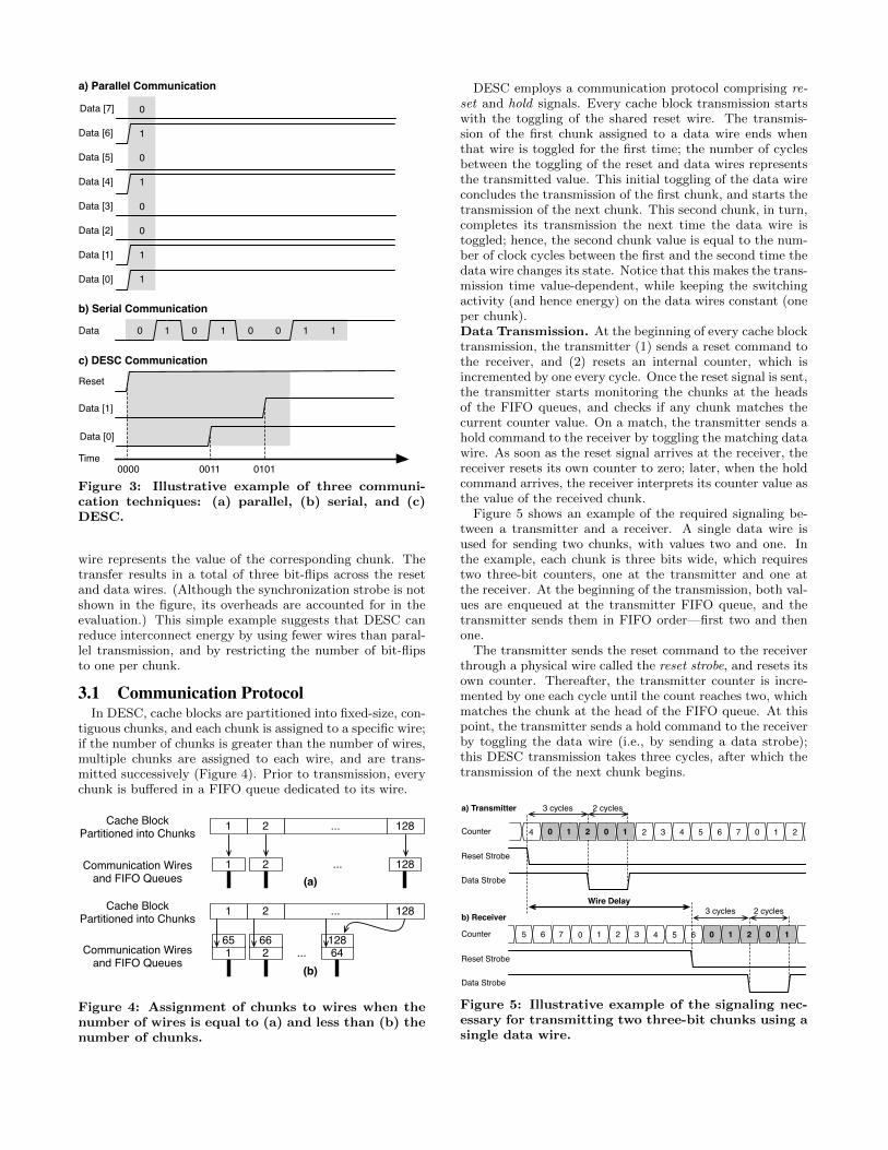
Figure 3 shows an example using three communicationtechniques: parallel, serial, and DESC. In the figure, onebyte (01010011) is sent from a transmitter to a receiver; allwires are assumed to hold zeroes prior to the transmission.With parallel data transfer, eight physical wires transfer thevalue in one cycle, which results in four bit-flips on the inter-connect. Serial data transfer requires only a single wire, butresults in longer transfer time (eight cycles); the result ofthis transmission is five bit-flips. DESC needs three wires—two for data and one for reset. The data byte is dividedinto two four-bit chunks, and each chunk is sent by tog-gling one of the two data wires. The reset wire is shared byall data wires to specify the start of the data transmission(before the transmission of a cache block); the number ofclock cycles between the reset signal and a bit-flip on a data
0
1
0
1
0
0
1
1
Data [7]
Data [6]
Data [5]
Data [4]
Data [3]
Data [2]
Data [1]
Data [0]
a) Parallel Communication
Data 0 1 0 1 0 0 1 1
b) Serial Communication
Reset
Data [1]
0000 01010011
c) DESC Communication
Time
Data [0]
Figure 3: Illustrative example of three communi-cation techniques: (a) parallel, (b) serial, and (c)DESC.
wire represents the value of the corresponding chunk. Thetransfer results in a total of three bit-flips across the resetand data wires. (Although the synchronization strobe is notshown in the figure, its overheads are accounted for in theevaluation.) This simple example suggests that DESC canreduce interconnect energy by using fewer wires than paral-lel transmission, and by restricting the number of bit-flipsto one per chunk.
3.1 Communication ProtocolIn DESC, cache blocks are partitioned into fixed-size, con-
tiguous chunks, and each chunk is assigned to a specific wire;if the number of chunks is greater than the number of wires,multiple chunks are assigned to each wire, and are trans-mitted successively (Figure 4). Prior to transmission, everychunk is bu↵ered in a FIFO queue dedicated to its wire.
(a)
Cache Block Partitioned into Chunks 1 2 ... 128
1 2 128...Communication Wiresand FIFO Queues
(b)
1 2 ... 128
...165
266
64128
Cache Block Partitioned into Chunks
Communication Wiresand FIFO Queues
Figure 4: Assignment of chunks to wires when thenumber of wires is equal to (a) and less than (b) thenumber of chunks.
DESC employs a communication protocol comprising re-
set and hold signals. Every cache block transmission startswith the toggling of the shared reset wire. The transmis-sion of the first chunk assigned to a data wire ends whenthat wire is toggled for the first time; the number of cyclesbetween the toggling of the reset and data wires representsthe transmitted value. This initial toggling of the data wireconcludes the transmission of the first chunk, and starts thetransmission of the next chunk. This second chunk, in turn,completes its transmission the next time the data wire istoggled; hence, the second chunk value is equal to the num-ber of clock cycles between the first and the second time thedata wire changes its state. Notice that this makes the trans-mission time value-dependent, while keeping the switchingactivity (and hence energy) on the data wires constant (oneper chunk).Data Transmission. At the beginning of every cache blocktransmission, the transmitter (1) sends a reset command tothe receiver, and (2) resets an internal counter, which isincremented by one every cycle. Once the reset signal is sent,the transmitter starts monitoring the chunks at the headsof the FIFO queues, and checks if any chunk matches thecurrent counter value. On a match, the transmitter sends ahold command to the receiver by toggling the matching datawire. As soon as the reset signal arrives at the receiver, thereceiver resets its own counter to zero; later, when the holdcommand arrives, the receiver interprets its counter value asthe value of the received chunk.
Figure 5 shows an example of the required signaling be-tween a transmitter and a receiver. A single data wire isused for sending two chunks, with values two and one. Inthe example, each chunk is three bits wide, which requirestwo three-bit counters, one at the transmitter and one atthe receiver. At the beginning of the transmission, both val-ues are enqueued at the transmitter FIFO queue, and thetransmitter sends them in FIFO order—first two and thenone.
The transmitter sends the reset command to the receiverthrough a physical wire called the reset strobe, and resets itsown counter. Thereafter, the transmitter counter is incre-mented by one each cycle until the count reaches two, whichmatches the chunk at the head of the FIFO queue. At thispoint, the transmitter sends a hold command to the receiverby toggling the data wire (i.e., by sending a data strobe);this DESC transmission takes three cycles, after which thetransmission of the next chunk begins.
1
1
12
12
00
004 2 3 4 5 6 7 0 1 2
0 1 2 3 4 5 65 6 7
Wire Delay
Counter
Counter
Data Strobe
Data Strobe
Reset Strobe
Reset Strobe
a) Transmitter
b) Receiver
3 cycles 2 cycles
3 cycles 2 cycles
Figure 5: Illustrative example of the signaling nec-essary for transmitting two three-bit chunks using asingle data wire.
Receiver
TransmitterReceiver
Transmitter
Chunks
Chunks
AccessReady
ReadData
WriteData
MatAddress
Ready
ReadData
WriteData
MatAddress
DES
C In
terf
ace
to th
e C
ache
C
ontr
olle
r
DES
C In
terf
ace
to th
e M
at
Con
trol
ler
Clock
ChunksT T'
Address Strobes (14 lines)
Write Data Strobes (16 lines)T T'
T T'T T'
TT'
T T'
T T'
ChunksTT'
TT'Read Data Strobes (16 lines)
DESC Controller
Reset/Write Skip StrobeSyncronization Strobe
Read Skip Strobe
DESC Controller
......
...
......
...
Figure 6: Illustrative example of the interface that connects a DESC transmitter and receiver on the cachecontroller to a DESC transmitter and receiver on a mat controller. Only a part of the block transfer is shownin the figure for simplicity. T and T’ indicate toggle generator and toggle detector, respectively.
Ultimately, strobe signals sent by the transmitter arriveat the receiver. There, the first reset command resets thereceiver’s counter to zero. Three cycles later, a hold strobearrives that makes the receiver latch in “two” as the value ofthe first chunk. Similarly, another data strobe indicating ahold command results in receiving the value “one”.Synchronization. The transmitter and the receiver in-volved in a data transfer need to operate synchronouslywith respect to either a global clock signal, or a local point-to-point synchronization strobe. In a synchronous cachedesign, all DESC controllers would be synchronized usingthe cache clock distribution network, whereas in an asyn-chronous cache (i.e., an ATM controlled cache [20]), a syn-chronization strobe between the cache controller and matswould be necessary. This paper applies DESC to asyn-chronous last-level caches due to their superior power ef-ficiency [20, 21]. The transmitter and receiver counters op-erate at the same clock frequency (possibly with di↵erentclock phases). This requires a dedicated wire carrying theclock information from the transmitter to the receiver. Toreduce the number of transitions on this wire, DESC gen-erates a synchronization strobe signal that toggles at halfthe frequency of the clock, but triggers the receiver at bothrising and falling edges.
3.2 Applying DESC to Last-Level CachesFigure 7 shows an example last-level cache system with a
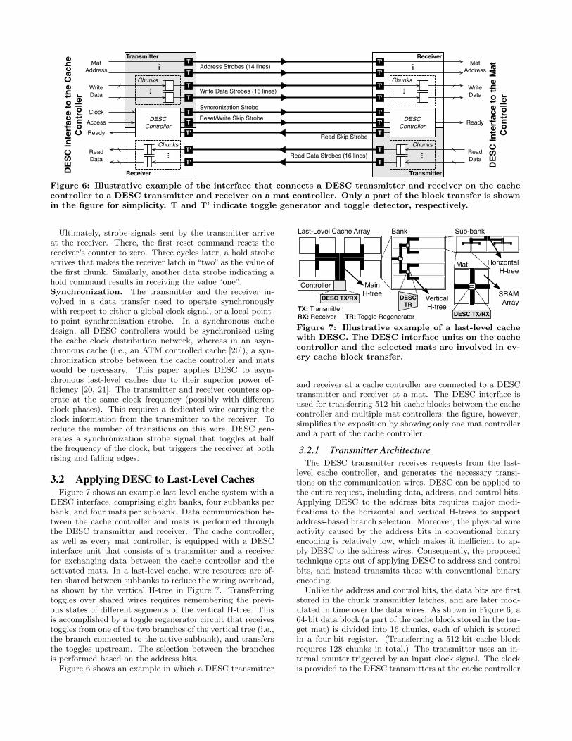
DESC interface, comprising eight banks, four subbanks perbank, and four mats per subbank. Data communication be-tween the cache controller and mats is performed throughthe DESC transmitter and receiver. The cache controller,as well as every mat controller, is equipped with a DESCinterface unit that consists of a transmitter and a receiverfor exchanging data between the cache controller and theactivated mats. In a last-level cache, wire resources are of-ten shared between subbanks to reduce the wiring overhead,as shown by the vertical H-tree in Figure 7. Transferringtoggles over shared wires requires remembering the previ-ous states of di↵erent segments of the vertical H-tree. Thisis accomplished by a toggle regenerator circuit that receivestoggles from one of the two branches of the vertical tree (i.e.,the branch connected to the active subbank), and transfersthe toggles upstream. The selection between the branchesis performed based on the address bits.
Figure 6 shows an example in which a DESC transmitter
Last-Level Cache Array
Mat
Bank Sub-bank
VerticalH-tree
MainH-tree
HorizontalH-tree
DESC TX/RX
DESC TX/RX
TX: TransmitterRX: Receiver TR: Toggle Regenerator
SRAMArray
DESC TR
Controller
Figure 7: Illustrative example of a last-level cachewith DESC. The DESC interface units on the cachecontroller and the selected mats are involved in ev-ery cache block transfer.
and receiver at a cache controller are connected to a DESCtransmitter and receiver at a mat. The DESC interface isused for transferring 512-bit cache blocks between the cachecontroller and multiple mat controllers; the figure, however,simplifies the exposition by showing only one mat controllerand a part of the cache controller.
3.2.1 Transmitter ArchitectureThe DESC transmitter receives requests from the last-
level cache controller, and generates the necessary transi-tions on the communication wires. DESC can be applied tothe entire request, including data, address, and control bits.Applying DESC to the address bits requires major modi-fications to the horizontal and vertical H-trees to supportaddress-based branch selection. Moreover, the physical wireactivity caused by the address bits in conventional binaryencoding is relatively low, which makes it ine�cient to ap-ply DESC to the address wires. Consequently, the proposedtechnique opts out of applying DESC to address and controlbits, and instead transmits these with conventional binaryencoding.
Unlike the address and control bits, the data bits are firststored in the chunk transmitter latches, and are later mod-ulated in time over the data wires. As shown in Figure 6, a64-bit data block (a part of the cache block stored in the tar-get mat) is divided into 16 chunks, each of which is storedin a four-bit register. (Transferring a 512-bit cache blockrequires 128 chunks in total.) The transmitter uses an in-ternal counter triggered by an input clock signal. The clockis provided to the DESC transmitters at the cache controller

interface. When there is an ongoing data transfer, the clocksignal is used to generate a synchronization strobe with atoggle generator, as shown in Figure 8-a, and is sent to theDESC receiver at the mat controller. The receiver recoversthe clock from the synchronization strobe using a toggle de-tector as shown in Figure 8-b. The recovered clock triggersthe internal counters of the receiver and the transmitter atthe mat controller.
b) Toggle Detector
Input
Output
Delayed Inputd
DInputOutput
Delayed Inputd
a) Toggle Generator
Output
Clock
Enable LEnable Output
Latch Input
c) Toggle Regenerator
Input 0
Select
Input 1
Output
L Output
Input 0
Input 1
Select
Select
Figure 8: Illustrative example of the toggle gener-ator (a), detector (b), and regenerator (b) used byDESC.
3.2.2 Receiver ArchitectureThe job of the DESC receiver is to detect the communica-
tion strobes sent by the transmitter, and to recover the datavalues. The DESC receiver consists of an internal counterand 16 chunk receivers. Each chunk receiver monitors astrobe wire to detect value changes. Once a strobe signalarrives at the receiver, the counter value is loaded into afour-bit register. Because of the equalized transmission de-lay of the wires in the cache H-tree, the content of the DESCreceiver counter at the time the strobe is received is alwaysthe same as the content of the transmitter counter at thetime the strobe is transmitted, which allows the chunk re-ceiver to recover the original data sent by the transmitter.After all data chunks are received, a ready signal marks theend of the data transfer.
3.2.3 Handling ECC ChecksApplying DESC to an LLC requires no modifications to
the SRAM arrays since data are stored in standard binaryformat. This makes it possible to use conventional error cor-recting codes (ECC) to protect the memory arrays. How-ever, DESC creates a new set of challenges that must bemet to protect the H-trees. Unlike conventional binary en-coding, DESC transfers a chunk of data using a single tran-sition on a wire; as a result, an error in the H-trees a↵ectsa chunk of information, and may corrupt up to four bits.Overcoming this problem requires adopting a carefully de-signed data layout for the parity bits used in single-errorcorrection, double-error detection (SECDED) ECC.
Similar to conventional SECDED ECC, DESC uses par-ity bits to protect the H-trees and the SRAM arrays. Extrawires are added to the data bus to transfer a set of paritychunks (Figure 9). Each parity chunk is transferred by asingle transition over ECC wires, and contains four paritybits, each of which belongs to a di↵erent data segment. Forexample, the (137, 128) Hamming code requires nine paritybits to protect a 128-bit data segment [22], and DESC sup-ports this scheme by adding nine additional wires. A cacheblock is partitioned into four 128-bit data segments, eachof which is augmented with nine parity bits. (ConventionalECC schemes use similar interleaving techniques for betterprotection against multiple adjacent errors [23].) Therefore,every data chunk contains at most one bit from each datasegment; similarly, each parity chunk contains one paritybit from each segment. This guarantees that a single errorin the H-trees cannot corrupt more than one bit from eachsegment. Similarly, a double error in a data segment canbe detected because two errors in the H-trees may a↵ect nomore than two bits per segment. This allows DESC to sup-port conventional SECDED ECC. So long as the segmentsare narrower than the data bus, DESC can accommodateconventional SECDED ECC without additional parity bits.This scheme is extendible to cache architectures with sepa-rate storage for ECC [24].
Conventional ECC Encoders
H
H
H
H
Stor
ed 5
12-b
it D
ata
Blo
ck
SRAM Arrays
d: correct data bit p: parity bit x: corrupted bit
...
Conventional ECC Decoders
✔
✔
✔
✔
Ret
rieve
d 51
2-bi
t Dat
a B
lock
...
paritydata
...
dddd
dddd
pppp
pppp
...
...
...
...
...
...
...
...
... error
pppp
pppp
dddd
xdxx
...
...
...
...
...
...
...
...
parity data
Figure 9: Illustrative example of ECC bits in DESC.
3.3 Energy and Delay OptimizationsDESC exploits data locality and null block prevalence in
the last-level cache to optimize power and delay. By default,every chunk requires a single bit-flip between a transmitterand the corresponding receiver. This sets a lower bound onthe number of required bit-flips to transmit a cache block; forexample, to transmit a 512-bit cache block from a transmit-ter comprising 128 chunk transmitters, where a data chunkis four bits, 128 transitions are needed on the data wires.Experiments show that a significant number of the chunkvalues transferred using DESC are either zeroes or the sameas the values transferred on the same wires in the previouscycle. DESC supports a value skipping mechanism to reducethe unnecessary energy and delay due to these repeated ornull chunks.
DESC defines a time window during which a block istransferred. Figure 10-a shows an example time window.The window opens with a reset signal and closes with thelast chunk signal. In this example, a data block consist-ing of four chunks (0, 0, 5, and 0) is transferred using five

bit-flips. Figure 10-b illustrates how the same chunk val-ues are communicated with value skipping in DESC. Thetime window is defined by two bit-flips on the reset/skipwire, and each non-zero chunk (such as 5 in the figure) istransferred by a bit-flip within the time window. Thosewires that remain silent over the duration of the time win-dow are set to zeroes at the end of the transfer; hence, thefour chunk values are transferred using three bit-flips. Thisscheme allows DESC to selectively specify a subset of thechunks to get assigned a predefined value at the cost of abit-flip on the shared reset/skip wire. Unlike DESC, ex-isting dynamic power optimization schemes [15, 12] requiretransferring extra information per chunk to support similarskipping operations. (As an alternative, these existing meth-ods can implement value skipping at the cache block level toreduce the overheads; however, this reduces the e↵ectivenessof these schemes.) For example, bus invert coding [15] canimplement zero skipping with control overheads. To accom-plish this, every chunk would need to determine if its valueis skipped. Combining this new feature with the originalbus invert coding results in three data transfer modes perchunk (non-inverted, inverted, and skipped). This requiresextra wires and results in energy overheads. (A compari-son against zero compression and bus invert coding + zeroskipping is presented in Section 5.)
a) Basic DESC a) Zero Skipped DESC
reset
chunk [0]
chunk [2]
chunk [1]
chunk [3]
0
0
5
0
0 51 2 3 4
time windowcounter
reset/skip
chunk [0]
chunk [2]
chunk [1]
chunk [3]
0
0
5
0
51 2 3 4
time windowcounter
Figure 10: Illustrative example of time windows inthe basic (a) and zero skipped (b) DESC techniques.
In addition to energy, value skipping can also improvetransmission latency. Applying value skipping to DESC re-sults in a narrower time window since the skipped value isexcluded from the count list. As shown in Figure 10, zeroskipped DESC requires a time window of five cycles as op-posed to the six cycles needed in the basic DESC.
DESC implements value skipping at both the cache con-troller and mat interfaces. Figure 11 shows how the trans-mitter and the receiver skip a value. Prior to transmittinga chunk, the transmitter compares the chunk’s value to apre-determined “skip value”; on a match, the transmittersets an internal flag indicating that the chunk should beskipped; otherwise, the relevant chunk transmitter is acti-vated to send the data strobe. After sending the requiredstrobe signals for all unskipped data chunks, a skip signalindicating the end of the transmission is sent to the receiverby toggling the reset/skip wire. The receiver receives datastrobes for unskipped chunks only; receiving a skip signalfrom the transmitter before all data strobes are toggled isinterpreted as a skip command. When a skip command ar-rives at the receiver, the skip value is copied to all pendingchunks. A transition on the DESC reset/skip wire is inter-preted as (1) a counter reset command signaling the begin-
ning of a new cache block transfer if there is no incompletechunk at the receiver, or (2) a skip command if some ofthe chunk receivers have not yet received a signal from thetransmitter.
Skip Value
= Down Counter
D
load
=1=0...
T
T
...
from other chunk transmitters
Start
Input Chunks
Done
Chunk Transmitter
Reset/Skip Transmitter
...
a) Value Skipped DESC Transmitter
b) Value Skipped DESC Receiver
Skip Valuecount
T'
T'
Dload
Up Counter
reset
...
Chunk Receiver
Received Chunks
from other chunk receivers
Data Strobe
Reset/Skip Strobe
Figure 11: Illustrative example of value skipping. Tand T’ indicate toggle generator and toggle detector,respectively.
This paper experiments with two di↵erent variations ofvalue skipping on DESC: zero skipping and last-value skip-
ping.Zero Skipping. Zero is the most common chunk value readfrom the last-level cache. Studying the behavior of di↵erentapplications on an 8MB L2 cache with a 4-bit DESC inter-face, we find that 31% of the transmitted chunks are zeroes(Figure 12). This motivates us to employ zero skipping inDESC, wherein the skip value is set to zero.
0.00#
0.05#
0.10#
0.15#
0.20#
0.25#
0.30#
0.35#
0# 1# 2# 3# 4# 5# 6# 7# 8# 9# 10# 11# 12# 13# 14# 15#
Average'Frequ
ency'of'
Tran
sferred'Ch
unk'Va
lues'
Four8Bit'Chunk'Values'
Zero#Chunks# Non8Zero#Chunks#
Figure 12: Distribution of four-bit chunk valuestransferred between the L2 cache controller and thedata arrays.
We also considered adaptive techniques for detecting andencoding frequent non-zero chunks at runtime; however, theattainable delay and energy improvements are not apprecia-ble. This is because of the relatively uniform distribution ofchunk values other than zero, as seen in Figure 12.Last-Value Skipping. Last-value skipping sets the skip

value for each chunk to the previous value transmitted onthe wire assigned to that chunk. This technique creates moreopportunities for skipping. Figure 13 shows the measuredprobability of transmitting two consecutive data chunks withthe same values. On average, 39% of the transmitted chunkson a wire have the same value as the previous chunk.
0"
0.2"
0.4"
0.6"
0.8"
1"
Art"
Barnes"
CG"
Cholesky"
Equake"FFT" FT
"
Linear" LU
"MG"
Ocean"
Radix"
RayTrace"
Swim"
WaterJNsquared"
WaterJSpacial"
Geomean"
Frac%on
(of(C
hunks(
Figure 13: Fraction of chunks transferred betweenthe processor and the L2 cache that match the pre-viously transmitted chunk.
4. EXPERIMENTAL SETUPWe evaluate the area, frequency, and power overheads of
DESC by implementing it in Verilog HDL, and synthesizingthe proposed hardware. We apply the proposed techniquesto UCA and S-NUCA-1 [8] L2 caches, using a modified ver-sion of CACTI 6.5 [14] to evaluate the energy e�ciency andperformance potential. We also implement the dynamic zerocompression [12] and bus invert coding [15] techniques asbaselines. We simulate 16 memory-intensive parallel appli-cations, running on a heavily modified version of the SESCsimulator [25]. Using McPAT [26], we estimate the overallprocessor power with and without DESC at the L2 cache.
4.1 ArchitectureWe modify the SESC simulator [25] to model two di↵erent
kinds of systems: (1) a Niagara-like eight-core processor, and(2) a single-threaded out-of-order processor. Both systemshave an 8MB L2 cache, interfaced to two DDR3-1066 DRAMchannels. Table 1 shows the simulation parameters.
Multithreaded 8 in-order cores, 3.2 GHz,Core 4 HW contexts per core
Single-threaded 4-issue out-of-order core,128 ROB entries, 3.2 GHz
IL1 cache 16KB, direct-mapped, 64B block,(per core) hit/miss delay 2/2DL1 cache 16KB, 4-way, LRU, 64B block,(per core) hit/miss delay 2/2, MESI protocolL2 cache 8MB, 16-way, LRU, 64B block,(shared) hit/miss delay 19/12
Temperature 350 �K (77 �C)DRAM 2 DDR3-1066 memory channels, FR-FCFS
Table 1: Simulation parameters.
Large SRAM caches have a significant impact on the en-ergy and performance of microprocessors. Due to the largenumber of transistors dedicated to the last level cache, de-signing an energy-e�cient microprocessor necessitates opti-mizations that reduce excessive leakage energy in the SRAMcells and the peripheral circuitry. Such techniques can re-duce cache leakage by orders of magnitude. (See [27, 28, 29,30, 31, 32, 33, 34] for examples of recent industrial designswith low-leakage devices in caches.)
We use CACTI 6.5 and SESC to explore the design spaceof the L2 cache, searching for the most energy e�cient tech-nology for the SRAM cells and the peripheral circuitry. Thedesign options in this exploration are ITRS high perfor-mance (HP), ITRS low power (LOP), and ITRS low standbypower (LSTP) devices [14]. In addition to the cell technolo-gies, we explore the energy e�ciency of the L2 cache forvarious bank counts (from 2 to 64) and data H-tree widths(from 8 to 512 bits). The goal is to set the most energye�cient configuration for the baseline L2 cache. Figure 14shows the relative cache energy, the overall execution time,and the processor energy averaged over all 16 applications.2
The results show that using LSTP technology for both theSRAM cells and the peripheral circuitry leads to a significantenergy reduction in the L2 cache at the cost of a negligibleloss in performance.3 As a result, the most energy e�cientL2 cache configuration consists of 8 banks with 64-bit dataH-trees, implemented with LSTP devices, which minimizesboth the L2 cache and total processor energy. This config-uration adds only 2% overhead to the total execution timecompared to the fastest L2 cache implemented with HP de-vices.
We modify SESC to support multiple interfaces at the L2cache for conventional binary transmission, bus-invert cod-ing [15], dynamic zero compression [12], S-NUCA-1 [8], andDESC. The L2 cache decodes an input address to activatea wordline in the data and tag arrays, which are co-located.The contents of a row are sensed and read out through thebitlines. On a hit, the comparator logic selects one way ofthe data array to be transferred on the H-trees.
Because bus-invert coding and dynamic zero compressionare sensitive to the number of bus segments, we find thebest segment size for each and use it in the baselines.4 Forfurther energy e�ciency, we also combine bus invert codingwith a zero skipping mechanism that eliminates unneces-sary bit-flips when transferring zero values. We evaluatetwo variants of zero skipped bus invert coding. First, weassume that an extra wire is employed for transferring thezero skipping signal per data segment, which results in alarge number of extra wires. This scheme takes into accountthe flips that would occur on the extra wires when decidingthe best encoding scheme for each segment. In addition tothis sparse representation, we also experiment with a denserrepresentation that uses a single binary number to encodethe transmission mode for all segments. This denser rep-resentation reduces the number of extra wires, but incursadditional decoding and encoding overheads.
Figure 15 shows the L2 cache energy for these techniquesnormalized to binary encoding. We select the best configura-tion for each technique as a baseline, and use these baselinesto make comparisons against DESC. Finally, we implementthree versions of DESC: basic (i.e., no value skipping), zeroskipped (Section 3.3), and last-value skipped (Section 3.3).
2Although we do a full design space exploration on the number of
banks and bus width for all device types, the figure illustrates a rep-resentative subset of the results for clarity.3Although using high-performance devices in both the cells and the
periphery results in approximately 2⇥ faster access time comparedto low standby power devices, the end-to-end system performanceexhibits less than 2% sensitivity to this di↵erence.4The paper ignores energy and latency overheads of the necessary
control logic in these baseline schemes–e.g., population counters andzero detection logic.

0"
100"
200"
300"
400"Sta*c"Energy" Dynamic"Energy"
LSTP%HP LSTP%LOP LSTP%LSTPHP%HP HP%LOP HP%LSTP LOP%HP LOP%LOP LOP%LSTP
L2 E
ner
gy
Norm
aliz
ed t
o 8
b
anks,
64-b
it
bus,
LST
P-LS
TP
8 banks, 64-bit bus
0"
0.5"
1"
1.5"
2"
LSTP%HP LSTP%LOP LSTP%LSTPHP%HP HP%LOP HP%LSTP LOP%HP LOP%LOP LOP%LSTP
Exec
uti
on T
ime
Norm
aliz
ed t
o 8
b
anks,
64-b
it b
us,
LS
TP-
LST
P
8 banks, 64-bit bus
0"
10"
20"
30"
LSTP%HP LSTP%LOP LSTP%LSTPHP%HP HP%LOP HP%LSTP LOP%HP LOP%LOP LOP%LSTPTota
l Pr
oce
ssor
Ener
gy
Norm
aliz
ed t
o 8
b
anks,
64-b
it
bus,
LST
P-LS
TP
8 banks, 64-bit bus
Figure 14: Design space exploration of the L2 cache for energy and execution time.
0"
0.2"
0.4"
0.6"
0.8"
1"
1.2"
Dynamic"Zero"Compression"
Bus"Invert"Coding"
Bus"Invert"Coding"+"Zero"
Skipping"
Bus"Invert"+"Encoded"Zero"
Skipping"
L2#Ene
rgy#Normalized
#to#
Bina
ry#Encod
ing#
64Bbit" 32Bbit" 16Bbit" 8Bbit" 4Bbit"
�"�" �" �"
Figure 15: L2 cache energy as a function of the datasegment size for the Dynamic Zero Compression,Bus Invert Coding, Bus Invert + Zero Skipping, andBus Invert + Encoded Zero Skipping schemes. Thebest configuration for each scheme (marked with astar) is selected as a baseline for evaluation.
4.2 ApplicationsEvaluated parallel workloads represent a mix of sixteen
data-intensive applications from Phoenix [35], SPLASH-2 [36],SPEC OpenMP [37], and NAS [38] suites. We also assessthe tolerance of single threaded applications to the accesslatency of DESC by evaluating eight applications from theSPEC 2006 suite. In this experiment, we use SimPoint [39]and determine a representative 200 million instruction re-gion from each SPEC 2006 application to reduce the execu-tion time. The parallel applications are simulated to com-pletion. Table 2 summarizes the evaluated benchmarks andtheir input sets. All applications are compiled using GCCwith the -O3 optimization flag.
4.3 SynthesisWe evaluate the area and power overheads of DESC by
implementing it in Verilog HDL, and synthesizing the design
Benchmarks Suite Input
Parallel
Linear Regression Phoenix 50MB key fileMG NAS OpenMP Class ACG NAS OpenMP Class A
Swim-Omp SPEC OpenMP MinneSpec-LargeEquake-Omp SPEC OpenMP MinneSpec-LargeArt-Omp SPEC OpenMP MinneSpec-LargeBarnes SPLASH-2 16K Particles
Cholesky SPLASH-2 tk 15.0Ocean SPLASH-2 514⇥514 oceanFFT SPLASH-2 1M pointsRadix SPLASH-2 2M integersLU SPLASH-2 512⇥512 matrix,
16⇥16 blocksOcean SPLASH-2 258⇥258 ocean
RayTrace SPLASH-2 carWater-Spatial SPLASH-2 512 molecules
Water-NSquared SPLASH-2 512 molecules
Sin
gle-threaded bzip2 SPECint 2006 reference
mcf SPECint 2006 referenceomnetpp SPECint 2006 referencesjeng SPECint 2006 referencelbm SPECfp 2006 referencemilc SPECfp 2006 referencenamd SPECfp 2006 referencesoplex SPECfp 2006 reference
Table 2: Applications and data sets.
using Cadence Encounter RTL Compiler [40] with FreePDK [41]at 45nm. The results are then scaled to 22nm (relevant pa-rameters are shown in Table 3).
Technology Voltage FO4 Delay45nm 1.1 V 20.25ps22nm 0.83 V 11.75ps
Table 3: Technology parameters [42, 43].
5. EVALUATIONWe first present synthesis results on the area, power, and
delay figures for the DESC transmitter and receiver. Next,we compare cache energy, power, and delay when usingDESC and conventional cache interfaces; for the latter, we

0"
0.5"
1"
1.5"
2"
Art"
Barnes"
CG"
Cholesky"
Equake"
FFT" FT
"
Linear"
LU"
MG"
Ocean"
Radix"
RayTrace"
Swim"
WaterHNsquared"
WaterHSpacial"
Geomean"
L2#Cache
#Ene
rgy#Normalized
#to#
Conve7
onal#Binary#En
coding# ConvenLonal"Binary" Dynamic"Zero"Compression" Bus"Invert"Coding" Zero"Skipped"Bus"Invert"
Encoded"Zero"Skipped"Bus"Invert" Basic"DESC" Zero"Skipped"DESC" Last"Value"Skipped"DESC"
Figure 16: L2 cache energy achieved by di↵erent data transfer techniques.
experiment with baselines incorporating bus invert codingand dynamic zero compression. We then evaluate the impactof DESC on overall system energy e�ciency, and conduct acache design-space exploration over all sixteen applications.We also evaluate applying DESC to an S-NUCA-1 cache.We study the sensitivity of DESC to the number of cachebanks, H-tree width, and chunk size. We then evaluate theperformance and energy potential of DESC under SECDEDECC. Finally, we assess the performance impact of DESCwhen running latency sensitive, single threaded applications.
5.1 Synthesis ResultsSynthesis results on the area, power, and delay contribu-
tions of the DESC transmitter and receiver are shown inFigure 17. A synthesized DESC interface occupies 2120µm2
at each cache mat, which adds less than 2% area overheadto the mats, and a total area overhead of 1% to the 8MB L2cache. The peak power consumption of a DESC interface,including the transmitter and the receiver, is 46mW . (No-tice that DESC consumes dynamic power only during datatransfers.) A pair of fully synthesized DESC interfaces adds625ps of logic delay to the round trip cache access time.Power, delay, and area can be further improved by usingcustom circuit design rather than synthesis.
0"
500"
1000"
1500"
2000"
2500"
Transmi-er" Receiver"
Area%(um2)%
0"
5"
10"
15"
20"
25"
30"
Transmi-er" Receiver"
Peak%Power%(mW)%
0"
0.05"
0.1"
0.15"
0.2"
0.25"
0.3"
0.35"
Transmi-er" Receiver"
Delay%(ns)%
Figure 17: Synthesis results for DESC transmitterand receiver, each comprising 128 chunks.
5.2 EnergySimulation results on the L2 cache energy are shown in
Figure 16. Dynamic zero compression, bus invert coding,and zero skipped bus invert coding result in an average of10%, 19%, and 20% reduction in the overall cache energy,
respectively; basic DESC provides 11% cache energy sav-ings, which is better than zero compression, but worse thanbus invert coding. This is due to the minimum dynamic en-ergy required on the interconnect, even for applications withfew bit flips—CG, Cholesky, Equake, Radix, and Water-Nsquared.
Applying value skipping to DESC results in a significantenergy reduction. Zero skipped DESC reduces overall cacheenergy by 1.81⇥ on average, while last-value skipped DESCachieves a 1.77⇥ energy reduction. Although the frequencyof skipped values in the last-value skipped DESC is higherthan that in the zero-skipped DESC (Figures 12 and 13), thelatter shows superior energy e�ciency because of the loweraccess energy. In the last-value skipped DESC, the cachecontroller needs to track the last values written to everymat. This requires extra storage at the cache controller torecord the last value exchange with every mat, in additionto broadcasting data bits for each write operation acrosssubbanks (through the vertical and horizontal H-trees, asshown in Figure 7). As a result, communication in the last-value skipped DESC consumes higher energy.
Figure 18 shows static and dynamic energy components ofthe L2 cache for di↵erent data transfer techniques, averagedover all applications. The results show that the superiorenergy e�ciency of zero skipped DESC is achieved througha 2⇥ reduction in dynamic cache energy, even though it addsa 3% static energy overhead to the baseline conventionalcache.
0" 0.1" 0.2" 0.3" 0.4" 0.5" 0.6" 0.7" 0.8" 0.9" 1"
Conven2onal"Binary"Dynamic"Zero"Compression"
Bus"Invert"Coding"Zero"Skipped"Bus"Invert"
Encoded"Zero"Skipped"Bus"Invert"Basic"DESC"
Zero"Skipped"DESC"Last"Value"Skipped"DESC"
Frac%on(of(Overall(Cache(Energy(
Sta2c"Energy" Dynamic"Energy"
Figure 18: Contribution of dynamic and static en-ergy components to the overall L2 cache energy fordi↵erent data transfer techniques.
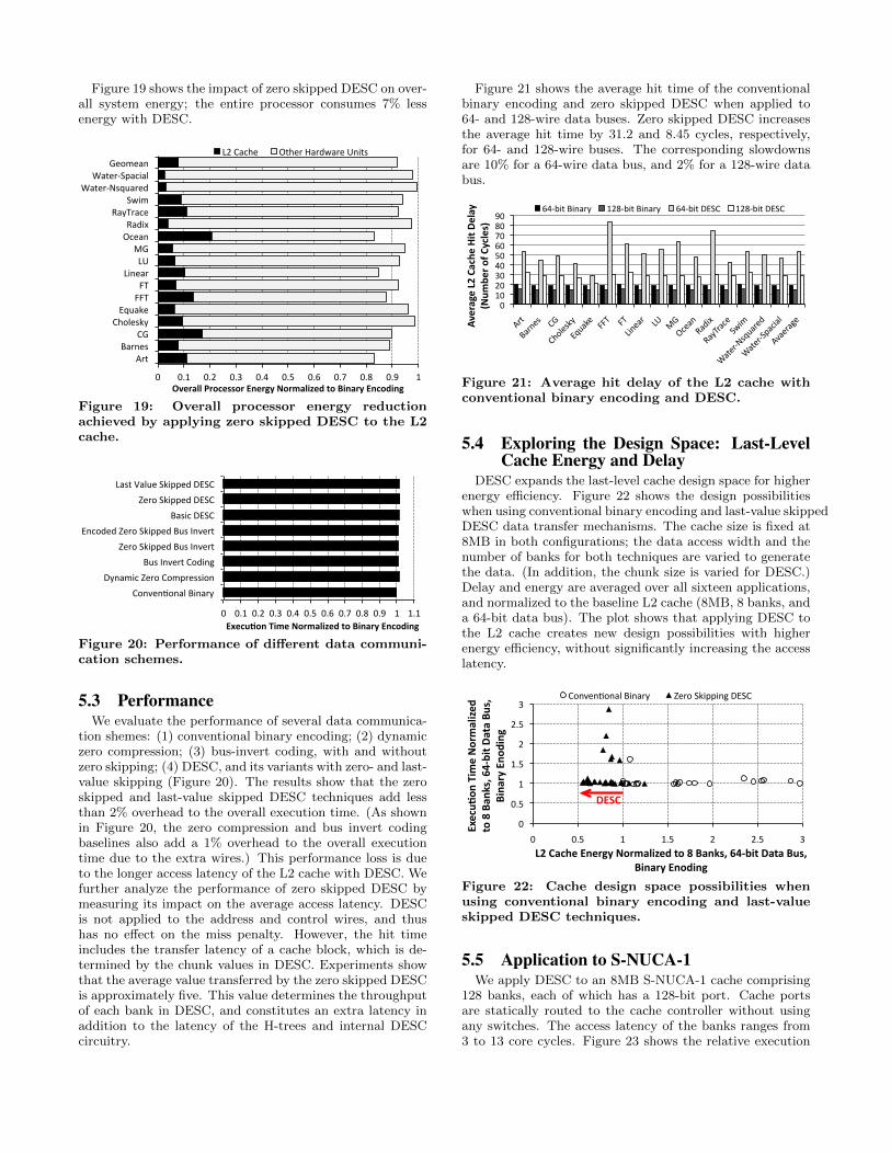
Figure 19 shows the impact of zero skipped DESC on over-all system energy; the entire processor consumes 7% lessenergy with DESC.
0" 0.1" 0.2" 0.3" 0.4" 0.5" 0.6" 0.7" 0.8" 0.9" 1"
Art"Barnes"
CG"Cholesky"Equake"
FFT"FT"
Linear"LU"MG"
Ocean"Radix"
RayTrace"Swim"
WaterNNsquared"WaterNSpacial"
Geomean"
Overall'Processor'Energy'Normalized'to'Binary'Encoding'
L2"Cache" Other"Hardware"Units"
Figure 19: Overall processor energy reductionachieved by applying zero skipped DESC to the L2cache.
0" 0.1" 0.2" 0.3" 0.4" 0.5" 0.6" 0.7" 0.8" 0.9" 1" 1.1"
Conven2onal"Binary"Dynamic"Zero"Compression"
Bus"Invert"Coding"Zero"Skipped"Bus"Invert"
Encoded"Zero"Skipped"Bus"Invert"Basic"DESC"
Zero"Skipped"DESC"Last"Value"Skipped"DESC"
Execu&on)Time)Normalized)to)Binary)Encoding)
Figure 20: Performance of di↵erent data communi-cation schemes.
5.3 PerformanceWe evaluate the performance of several data communica-
tion shemes: (1) conventional binary encoding; (2) dynamiczero compression; (3) bus-invert coding, with and withoutzero skipping; (4) DESC, and its variants with zero- and last-value skipping (Figure 20). The results show that the zeroskipped and last-value skipped DESC techniques add lessthan 2% overhead to the overall execution time. (As shownin Figure 20, the zero compression and bus invert codingbaselines also add a 1% overhead to the overall executiontime due to the extra wires.) This performance loss is dueto the longer access latency of the L2 cache with DESC. Wefurther analyze the performance of zero skipped DESC bymeasuring its impact on the average access latency. DESCis not applied to the address and control wires, and thushas no e↵ect on the miss penalty. However, the hit timeincludes the transfer latency of a cache block, which is de-termined by the chunk values in DESC. Experiments showthat the average value transferred by the zero skipped DESCis approximately five. This value determines the throughputof each bank in DESC, and constitutes an extra latency inaddition to the latency of the H-trees and internal DESCcircuitry.
Figure 21 shows the average hit time of the conventionalbinary encoding and zero skipped DESC when applied to64- and 128-wire data buses. Zero skipped DESC increasesthe average hit time by 31.2 and 8.45 cycles, respectively,for 64- and 128-wire buses. The corresponding slowdownsare 10% for a 64-wire data bus, and 2% for a 128-wire databus.
0"10"20"30"40"50"60"70"80"90"
Art"
Barnes"
CG"
Cholesky"
Equake"FFT" FT
"
Linear" LU
"MG"
Ocean"
Radix"
RayTrace"
Swim"
WaterMNsquared"
WaterMSpacial"
Avaerage"
Average'L2'Ca
che'Hit'Delay'
(Num
ber'of'Cycles)'
64Mbit"Binary" 128Mbit"Binary" 64Mbit"DESC" 128Mbit"DESC"
Figure 21: Average hit delay of the L2 cache withconventional binary encoding and DESC.
5.4 Exploring the Design Space: Last-LevelCache Energy and Delay
DESC expands the last-level cache design space for higherenergy e�ciency. Figure 22 shows the design possibilitieswhen using conventional binary encoding and last-value skippedDESC data transfer mechanisms. The cache size is fixed at8MB in both configurations; the data access width and thenumber of banks for both techniques are varied to generatethe data. (In addition, the chunk size is varied for DESC.)Delay and energy are averaged over all sixteen applications,and normalized to the baseline L2 cache (8MB, 8 banks, anda 64-bit data bus). The plot shows that applying DESC tothe L2 cache creates new design possibilities with higherenergy e�ciency, without significantly increasing the accesslatency.
0"
0.5"
1"
1.5"
2"
2.5"
3"
0" 0.5" 1" 1.5" 2" 2.5" 3"
Execu&
on)Tim
e)Normalized
)to)8)Ban
ks,)64;bit)D
ata)Bu
s,)
Bina
ry)Eno
ding)
L2)Cache)Energy)Normalized)to)8)Banks,)64;bit)Data)Bus,)Binary)Enoding)
Conven-onal"Binary" Zero"Skipping"DESC"
DESC)
Figure 22: Cache design space possibilities whenusing conventional binary encoding and last-valueskipped DESC techniques.
5.5 Application to S-NUCA-1We apply DESC to an 8MB S-NUCA-1 cache comprising
128 banks, each of which has a 128-bit port. Cache portsare statically routed to the cache controller without usingany switches. The access latency of the banks ranges from3 to 13 core cycles. Figure 23 shows the relative execution
time averaged over the sixteen applications for an S-NUCA-1 cache with zero skipped DESC. The results show that thezero skipped DESC incurs an execution time penalty of 1%over conventional binary encoding.
0"
0.2"
0.4"
0.6"
0.8"
1"
Art"
Barnes"CG"
Cholesky"
Equake"FFT" FT
"
Linear" LU
"MG"
Ocean"
Radix"
RayTrace"
Swim"
WaterJNsquared"
WaterJSpacial"
Geomean"
Execu&
on)Tim
e))of)D
ESC)+)S2
NUCA
21)Normalized
)to)S2
NUCA
21)
Figure 23: Normalized execution time when DESCis applied to an 8MB S-NUCA-1 cache.
As shown in Figure 24, DESC improves the energy of theS-NUCA-1 cache. The results indicate that zero skippedDESC improves cache energy by 1.62⇥, reduces the aver-age L2 power by 1.64⇥, and improves the L2 energy-delayproduct by 1.59⇥.
0"
0.2"
0.4"
0.6"
0.8"
1"
Art"
Barnes"CG"
Cholesky"
Equake"FFT" FT
"
Linear" LU
"MG"
Ocean"
Radix"
RayTrace"
Swim"
WaterJNsquared"
WaterJSpacial"
Geomean"
L2#Ene
rgy#of#DESC#+#S0
NUCA
01#Normalized
#to#S0
NUCA
01#
Figure 24: The energy of an 8MB S-NUCA-1 cachewith zero skipped DESC.
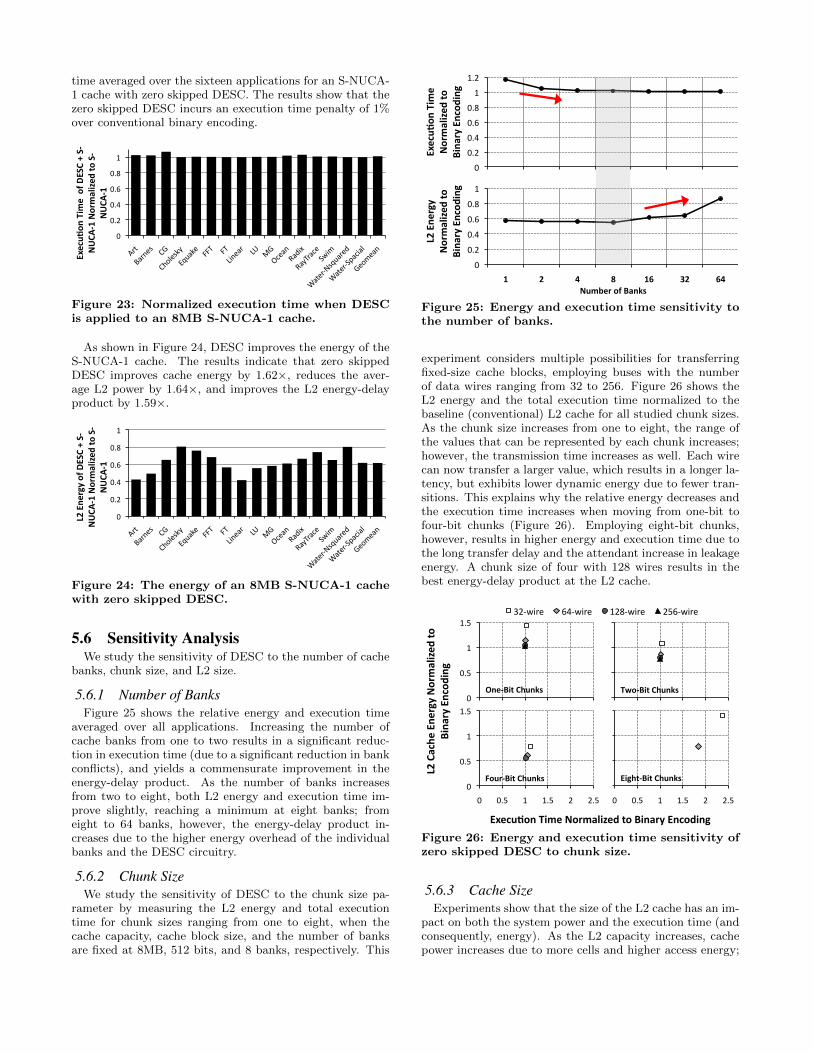
5.6 Sensitivity AnalysisWe study the sensitivity of DESC to the number of cache
banks, chunk size, and L2 size.
5.6.1 Number of BanksFigure 25 shows the relative energy and execution time
averaged over all applications. Increasing the number ofcache banks from one to two results in a significant reduc-tion in execution time (due to a significant reduction in bankconflicts), and yields a commensurate improvement in theenergy-delay product. As the number of banks increasesfrom two to eight, both L2 energy and execution time im-prove slightly, reaching a minimum at eight banks; fromeight to 64 banks, however, the energy-delay product in-creases due to the higher energy overhead of the individualbanks and the DESC circuitry.
5.6.2 Chunk SizeWe study the sensitivity of DESC to the chunk size pa-
rameter by measuring the L2 energy and total executiontime for chunk sizes ranging from one to eight, when thecache capacity, cache block size, and the number of banksare fixed at 8MB, 512 bits, and 8 banks, respectively. This
0"
0.2"
0.4"
0.6"
0.8"
1"
1.2"
Execu&
on)Tim
e)Normalized
)to)
Bina
ry)Encod
ing)
0"
0.2"
0.4"
0.6"
0.8"
1"
1) 2) 4) 8) 16) 32) 64)
L2)Ene
rgy)
Normalized
)to)
Bina
ry)Encod
ing)
Number)of)Banks)
Figure 25: Energy and execution time sensitivity tothe number of banks.
experiment considers multiple possibilities for transferringfixed-size cache blocks, employing buses with the numberof data wires ranging from 32 to 256. Figure 26 shows theL2 energy and the total execution time normalized to thebaseline (conventional) L2 cache for all studied chunk sizes.As the chunk size increases from one to eight, the range ofthe values that can be represented by each chunk increases;however, the transmission time increases as well. Each wirecan now transfer a larger value, which results in a longer la-tency, but exhibits lower dynamic energy due to fewer tran-sitions. This explains why the relative energy decreases andthe execution time increases when moving from one-bit tofour-bit chunks (Figure 26). Employing eight-bit chunks,however, results in higher energy and execution time due tothe long transfer delay and the attendant increase in leakageenergy. A chunk size of four with 128 wires results in thebest energy-delay product at the L2 cache.
L2#Cache
#Ene
rgy#Normalized
#to#
Bina
ry#Encod
ing#
Execu9on#Time#Normalized#to#Binary#Encoding#
32#wire( 64#wire( 128#wire( 256#wire(
0(
0.5(
1(
1.5(
0(
0.5(
1(
1.5(
0( 0.5( 1( 1.5( 2( 2.5( 0( 0.5( 1( 1.5( 2( 2.5(
One<Bit#Chunks# Two<Bit#Chunks#
Four<Bit#Chunks# Eight<Bit#Chunks#
Figure 26: Energy and execution time sensitivity ofzero skipped DESC to chunk size.
5.6.3 Cache SizeExperiments show that the size of the L2 cache has an im-
pact on both the system power and the execution time (andconsequently, energy). As the L2 capacity increases, cachepower increases due to more cells and higher access energy;

however, the total execution time decreases because of fewercache misses. For the evaluated multicore design, most ofthe L2 dynamic energy is consumed in the H-trees, becausethe LSTP transistors significantly reduce the static powerof the arrays and the peripheral circuits. Figure 27 showsthe impact of capacity on the L2 energy when the cache sizeranges from 512KB to 64MB. The results indicate that in-creasing the cache size results in higher energy consumptionfor both conventional binary and DESC. However, DESCimproves the average cache energy by 1.87⇥ to 1.75⇥, whenthe cache size ranges from 512K to 64MB.
0"
1"
2"
3"
4"
512KB" 1MB" 2MB" 4MB" 8MB" 16MB" 32MB" 64MB"
L2#Ene
rgy#Normalized
#to#an#
8MB#L2#with
#Binary#En
coding#
Conven2onal"Binary" DESC"
1.87×#
1.75×#
Figure 27: The impact of L2 capacity on cache en-ergy.
5.7 Performance and Energy Characterizationunder SECDED ECC
We apply DESC to an 8MB cache comprising eight banksprotected by SECDED ECC.We evaluate the execution timeand the L2 energy when the (72, 64) and (137, 128) Ham-ming codes are applied with binary encoding and DESC. Asshown in Figure 28, the zero skipped DESC incurs an aver-age execution time penalty of 1% over conventional binaryencoding.
0"0.1"0.2"0.3"0.4"0.5"0.6"0.7"0.8"0.9"1"
1.1"
Art"
Barnes" CG
"
Cholesky"
Equake"FFT" FT
"
Linear" LU
"MG
"
Ocean"Radix"
RayTrace"Swim"
WaterNNsquared"
WaterNSpacial"
Geomean"Ex
ecu&
on)Tim
e)Normalized
)to)646bit)B
inary)en
coding)
with
)646bit)D
ECDE
D)EC
C) 64N64"Binary" 128N128"Binary" 128N64"DESC" 128N128"DESC"
Figure 28: Normalized execution time for binaryencoding and DESC for various configurations (W-S), where W represents the number of data wiresand S is the segment size to which the Hammingcode is applied.
Figure 29 shows that the zero skipped DESC improvescache energy by 1.82⇥ and 1.92⇥ for the (72, 64) and (137,128) Hamming codes, respectively.
5.8 Impact on Latency ToleranceUnlike a throughput-oriented design such as the multicore
system with multithreaded cores evaluated in Sections 5.3 -5.7, a latency sensitive design may su↵er from a significantperformance degradation when using DESC. To study the
0"
0.2"
0.4"
0.6"
0.8"
1"
1.2"
Art"
Barnes" CG
"
Cholesky"
Equake"FFT" FT
"
Linear" LU
"MG
"
Ocean"Radix"
RayTrace"Swim"
WaterJNsquared"
WaterJSpacial"
Geomean"L2
#cache
#Ene
rgy#Normalized
#to#647bit#B
inary#en
coding#
with
#647bit#D
ECDE
D#EC
C#
64J64"Binary" 128J128"Binary" 128J64"DESC" 128J128"DESC"
Figure 29: Normalized L2 energy for binary en-coding and DESC for various configurations (W-S),where W represents the number of data wires andS is the segment size to which the Hamming code isapplied.
e↵ects of the long data transfer latency of DESC on suchsystems, we model an out-of-order processor running singlethreaded applications from the SPEC CPU 2006 suite [44].The simulation results indicate that applying DESC to theL2 increases the execution time by 6% on average (Fig-ure 30).
0" 0.1" 0.2" 0.3" 0.4" 0.5" 0.6" 0.7" 0.8" 0.9" 1" 1.1" 1.2"
BZIP2"LBM"MCF"MILC"
NAMD"OMNETPP"
SJENG"SOPLEX"
Geomean"
Figure 30: Execution time normalized to binary en-coding.
6. CONCLUSIONSWe have presented DESC, an energy-e�cient data ex-
change technique using synchronized counters. DESC cre-ates new opportunities for designing low power on-chip in-terconnects. We have seen that applying DESC to the L2cache can reduce overall cache energy by 1.81⇥ by lower-ing dynamic power at the cache H-tree. This results in 7%savings in overall processor energy at a cost of less than2% increase in the overall execution time, and a negligiblearea overhead. We have also observed that DESC achievesbetter power improvements compared to existing work onbus-invert coding and dynamic zero compression by exploit-ing more e�cient mechanisms for skipping redundant values.We conclude that DESC holds the potential to significantlyimprove the energy e�ciency of on-chip communication infuture computer systems.
7. ACKNOWLEDGMENTSThe authors would like to thank anonymous reviewers for
useful feedback. This work was supported in part by NSFgrant CCF-1217418.
8. REFERENCES[1] Nir Magen, Avinoam Kolodny, Uri Weiser, and Nachum
Shamir. Interconnect-power dissipation in a microprocessor.

International Workshop on System Level InterconnectPrediction, 2004.
[2] A.N. Udipi, N. Muralimanohar, and R. Balasubramonian.Non-uniform power access in large caches with low-swing wires.International Conference on High Performance Computing,2009.
[3] A. Lambrechts, P. Raghavan, M. Jayapala, F. Catthoor, andD. Verkest. Energy-aware interconnect optimization for acoarse grained reconfigurable processor. InternationalConference on VLSI Design, 2008.
[4] G. Chandra, P. Kapur, and K.C. Saraswat. Scaling trends forthe on chip power dissipation. International InterconnectTechnology Conference, 2002.
[5] Nikos Hardavellas, Michael Ferdman, Anastasia Ailamaki, andBabak Falsafi. Power scaling: the ultimate obstacle to 1k-corechips. Technical Report NWU-EECS-10-05, 2010.
[6] Bradford M. Beckmann and David A. Wood. TLC:Transmission line caches. International Symposium onMicroarchitecture, 2003.
[7] Hui Zhang and J. Rabaey. Low-swing interconnect interfacecircuits. International Symposium on Low Power Electronicsand Design, 1998.
[8] Changkyu Kim, Doug Burger, and Stephen W. Keckler. Anadaptive, non-uniform cache structure for wire-delaydominated on-chip caches. International Conference onArchitectural Support for Programming Languages andOperating Systems, 2002.
[9] Daniel Citron. Exploiting low entropy to reduce wire delay.IEEE Computer Architecture Letters, 2004.
[10] A. Seznec. Decoupled sectored caches: conciliating low tagimplementation cost. In International Symposium onComputer Architecture, 1994.
[11] Julien Dusser, Thomas Piquet, and Andre Seznec.Zero-Content Augmented Caches. Rapport de rechercheRR-6705, INRIA, 2008.
[12] Luis Villa, Michael Zhang, and Krste Asanovic. Dynamic zerocompression for cache energy reduction. InternationalSymposium on Microarchitecture, 2000.
[13] Rajeev Balasubramonian, Naveen Muralimanohar, KarthikRamani, and Venkatanand Venkatachalapathy.Microarchitectural wire management for performance andpower in partitioned architectures. International Symposiumon High-Performance Computer Architecture, 2005.
[14] N. Muralimanohar, R. Balasubramonian, and N. Jouppi.Optimizing NUCA organizations and wiring alternatives forlarge caches with CACTI 6.0. International Symposium onMicroarchitecture, 2007.
[15] Mircea R. Stan and Wayne P. Burleson. Bus-invert coding forlow-power I/O. IEEE Transactions on VLSI Systems, 1995.
[16] S. Kaxiras, Z. Hu, and M. Martonosi. Cache decay: Exploitinggenerational behavior to reduce cache leakage power.International Symposium on Computer Architecture, 2001.
[17] K. Flautner, N. S. Kim, S. Martin, D. Blaauw, and T. Mudge.Drowsy caches: simple techniques for reducing leakage power.International Symposium on Computer Architecture, 2002.
[18] Nam Sung Kim, David Blaauw, and Trevor Mudge. Leakagepower optimization techniques for ultra deep sub-micronmulti-level caches. International Conference onComputer-Aided Design, 2003.
[19] J. G. Proakis. Digital Communications. Third Edition,McGraw-Hill, 1995.
[20] K. Itoh, K. Sasaki, and Y. Nakagome. Trends in low- powerRAM circuit technologies. Symposium on Low PowerElectronics, 1994.
[21] J. Wuu, D. Weiss, C. Morganti, and M. Dreesen. Theasynchronous 24MB on-chip level-3 cache for a dual-coreItanium R�-family processor. International Solid-State CircuitsConference, 2005.
[22] C.W. Slayman. Cache and memory error detection, correction,and reduction techniques for terrestrial servers andworkstations. IEEE Transactions on Device and MaterialsReliability, 2005.
[23] Y.Q. Shi, Xi Min Zhang, Zhi-Cheng Ni, and N. Ansari.Interleaving for combating bursts of errors. IEEE Circuits andSystems Magazine, 2004.
[24] Doe Hyun Yoon and Mattan Erez. Memory mapped ecc:Low-cost error protection for last level caches. InternationalSymposium on Computer Architecture, 2009.
[25] Jose Renau et al. SESC simulator, Jan. 2005.http://sesc.sourceforge.net.
[26] Sheng Li, Jung Ho Ahn, Richard D. Strong, Jay B. Brockman,Dean M. Tullsen, and Norman P. Jouppi. McPAT: Anintegrated power, area, and timing modeling framework formulticore and manycore architectures. InternationalSymposium on Computer Architecture, 2009.
[27] K. Kanda, T. Miyazaki, Min Kyeong Sik, H. Kawaguchi, andT. Sakurai. Two orders of magnitude leakage power reductionof low voltage SRAMs by row-by-row dynamic VDD control(RRDV) scheme. International ASIC/SOC Conference, 2002.
[28] S. Rusu, S. Tam, H. Muljono, D. Ayers, and J. Chang. Adual-core multi-threaded xeon processor with 16MB L3 cache.International Solid-State Circuits Conference, 2006.
[29] Varghese George, Sanjeev Jahagirdar, Chao Tong, K. Smits,Satish Damaraju, Scott Siers, Ves Naydenov, TanveerKhondker, Sanjib Sarkar, and Puneet Singh. Penryn: 45-nmnext generation Intel Core 2 processor. Asian Solid-StateCircuits Conference, 2007.
[30] D. James. Intel Ivy Bridge unveiled - the first commercialtri-gate, high-k, metal-gate CPU. Custom Integrated CircuitsConference, 2012.
[31] E. Karl, Yih Wang, Yong-Gee Ng, Zheng Guo, F. Hamzaoglu,U. Bhattacharya, K. Zhang, K. Mistry, and M. Bohr. A4.6GHz 162MB SRAM design in 22nm tri-gate CMOStechnology with integrated active vmin-enhancing assistcircuitry. International Solid-State Circuits Conference, 2012.
[32] N. Maeda, S. Komatsu, M. Morimoto, and Y. Shimazaki. A0.41 ua standby leakage 32kb embedded SRAM withlow-voltage resume-standby utilizing all digital currentcomparator in 28nm hkmg CMOS. Symposium on VLSICircuits, 2012.
[33] Masaki Fujigaya, Noriaki Sakamoto, Takao Koike, TakahiroIrita, Kohei Wakahara, Tsugio Matsuyama, Keiji Hasegawa,Toshiharu Saito, Akira Fukuda, Kaname Teranishi, KazukiFukuoka, Noriaki Maeda, Koji Nii, Takeshi Kataoka, andToshihiro Hattori. A 28nm high-k metal-gate single-chipcommunications processor with 1.5GHz dual-core applicationprocessor and LTE/HSPA+-capable baseband processor.International Solid-State Circuits Conference, 2013.
[34] Fumihiko Tachibana, Osamu Hirabayashi, Yasuhisa Takeyama,Miyako Shizuno, Atsushi Kawasumi, Keiichi Kushida, AzumaSuzuki, Yusuke Niki, Shinichi Sasaki, Tomoaki Yabe, andYasuo Unekawa. A 27% active and 85% standby powerreduction in dual-power-supply SRAM using BL powercalculator and digitally controllable retention circuit.International Solid-State Circuits, 2013.
[35] Richard M. Yoo, Anthony Romano, and Christos Kozyrakis.Phoenix rebirth: Scalable MapReduce on a large-scaleshared-memory system. International Symposium onWorkload Characterization, 2009.
[36] S. C. Woo, M. Ohara, E. Torrie, J. P. Singh, and A. Gupta.The SPLASH-2 programs: Characterization andmethodological considerations. In International Symposiumon Computer Architecture, 1995.
[37] L. Dagum and R. Menon. OpenMP: An industry-standard APIfor shared-memory programming. IEEE ComputationalScience and Engineering, 1998.
[38] D. H. Bailey et al. NAS parallel benchmarks. Technical reportRNR-94-007., NASA Ames Research Center, 1994.
[39] Greg Hamerly, Erez Perelman, Jeremy Lau, and Brad Calder.Simpoint 3.0: Faster and more flexible program analysis.Journal of Instruction Level Parallelism, 2005.
[40] Encounter RTL compiler.http://www.cadence.com/products/ld/rtl_compiler/.
[41] Free PDK 45nm open-access based PDK for the 45nmtechnology node. http://www.eda.ncsu.edu/wiki/FreePDK.
[42] ITRS. International Technology Roadmap forSemiconductors.http://www.itrs.net/links/2010itrs/home2010.htm.
[43] Wei Zhao and Yu Cao. New generation of predictivetechnology model for sub-45nm design exploration.International Symposium on Quality Electronic Design, 2006.
[44] John L. Henning. SPEC CPU2006 benchmark descriptions.SIGARCH Computer Architecture News, 2006.