description features - princeton lcd driver ic tel: 886-66296288 ‧fax: 886-29174598 ‧ ‧2f, no....
TRANSCRIPT

PT6526LCD Driver IC
Tel: 886-66296288‧Fax: 886-29174598‧ http://www.princeton.com.tw‧2F, No. 233-1, Baociao Rd., Sindian Dist., New Taipei City 23145, Taiwan
DESCRIPTION PT6526 is a General Purpose LCD Driver IC utilizing CMOS Technology specially designed for electronic tuners controlled by microcontroller. It can drive up to a maximum of 204 segment outputs and can control up to 12 general purpose output ports. Pin assignments and application circuit are optimized for easy PCB layout and cost saving advantages.
APPLICATION • Frequency Display for Electronic Tuners
FEATURES • CMOS Technology • Up to 4 Common and 51 Segment Drivers • Up to 204 LCD Segments • Up to 12 General Purpose Output Ports • 1/4 Duty – 1/2 Bias or 1/4 Duty – 1/3 Bias Drive
Technique • No Decoder Intervention Necessary to Display the
Data • Power Saving Mode provided • Power Supply Voltage: 4.5V to 6V • CMOS/TTL compatible logic input pins • RC Oscillation Circuit • Available in 64-pin, LQFP
BLOCK DIAGRAM

PT6526
V1.2 2 February 2013
APPLICATION CIRCUITS 1/2 BIAS (NORMAL PANELS)
Notes: 1. C ≥ 0.047µF 2. 39KΩ ≥ R1 ≥ 1KΩ

PT6526
V1.2 3 February 2013
1/2 BIAS (LARGE PANELS)
Notes: 1. C ≥ 0.047µF 2. 10KΩ ≥ R ≥ 1KΩ
3. 39KΩ ≥ R1 ≥ 1KΩ
PT6526
V1.2 4 February 2013
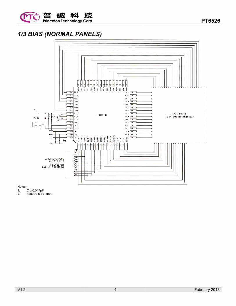
1/3 BIAS (NORMAL PANELS)
Notes: 1. C ≥ 0.047µF 2. 39KΩ ≥ R1 ≥ 1KΩ

PT6526
V1.2 5 February 2013
1/3 BIAS (LARGE PANELS)
Notes: 1. 10KΩ ≥ R ≥ 1KΩ 2. C ≥ 0.047µF 3. 39KΩ ≥ R1 ≥ 1KΩ

PT6526
V1.2 6 February 2013
ORDER INFORMATION Valid Part Number Package Type Top Code
PT6526-LQ 64 Pin, LQFP PT6526-LQ
PIN CONFIGURATION

PT6526
V1.2 7 February 2013
PIN DESCRIPTION Pin Name I/O Description Pin No.
SG1/P1 ~ SG12/P12 O Segment Driver Output/General Purpose Output Ports 1 ~ 12 SG13 ~ SG51 O Segment Driver Output Pins 13 ~ 51
COM1 ~ COM4 O Common Driver Output Pins 52 ~55 VDD - Power Supply 56
VDD1 -
Power Supply This pin is used to apply a 2/3 LCD Drive Bias Voltage. If the ½ Bias Drive Technique is used, this pin must be short to VDD2.
57
VDD2 -
Power Supply This pin is used to apply a 1/3 LCD Drive Bias Voltage. If the ½ Bias Drive Technique is used, this pin must be short to VDD1.
58
VSS - Ground 59 OSC I/O Oscillation Input / Output Pin 60
/INH I
Display OFF Control Pin If this pin is set to “LOW” (VSS), the display is forced to turn OFF. Output driver pins -- SG1/P1 to SG12/P12, SG13 to SG51, COM1 to COM4 are set to “LOW”. If this pin is set to “HIGH” (VDD), the display is turned ON. (see Note)
61
CE I Chip Enable Pin 62 CLK I Clock Input Pin 63 DI I Data Input Pin 64
Note: It must be noted that when the display is forcibly turned OFF, the serial data transfers can still be performed.

PT6526
V1.2 8 February 2013
INPUT/OUTPUT CONFIGURATIONS The schematic diagrams of the input and output circuits of the logic section are shown below:
INPUT PIN: CLK, CE, DI, /INH
OUTPUT PIN: COM1 TO COM4, SG13 TO SG51
OUTPUT PIN: SG1/P1 TO SG12/P12

PT6526
V1.2 9 February 2013
UNCTION DESCRIPTION CONTROL DATA BITS CU: NORMAL MODE CURRENT DRAIN CONTROL DATA BIT This control bit is used to select the current drain (either Normal Current Drain or Low Current Drain) in the Normal Mode. Please refer to the table below.
CU Current Drain (under the Normal Mode) 0 Normal Current Drain (IDD2, IDD3) 1 Low Current Drain (IDD4, IDD5)
It should be noted that when the Low Current Drain is selected by setting the CU to “1”, the output waveforms of the common and segment driver are easily distorted since the capacity to supply the current to the LCD panel from the Common and Segment Pins is less than capacity under the Normal Current Drain (CU = “0”).
P0 TO P3: SEGMENT / GENERAL PURPOSE OUTPUT PORT SELECT BITS These control bits are used to select the function of the SG1/P1 to SG12/P12 output pins (either Segment Output Pins or General Purpose Output Pins). Please refer to the table below.
Control Data Output Pins
P0 P1 P2 P3 SG1/P1
SG2/P2
SG3/P3
SG4/P4
SG5/P5
SG6/P6
SG7/P7
SG8/P8
SG9/P9
SG10/P10
SG11/P11
SG12/P12
0 0 0 0 SG1 SG2 SG3 SG4 SG5 SG6 SG7 SG8 SG9 SG10 SG11 SG12 0 0 0 1 P1 SG2 SG3 SG4 SG5 SG6 SG7 SG8 SG9 SG10 SG11 SG12 0 0 1 0 P1 P2 SG3 SG4 SG5 SG6 SG7 SG8 SG9 SG10 SG11 SG12 0 0 1 1 P1 P2 P3 SG4 SG5 SG6 SG7 SG8 SG9 SG10 SG11 SG12 0 1 0 0 P1 P2 P3 P4 SG5 SG6 SG7 SG8 SG9 SG10 SG11 SG12 0 1 0 1 P1 P2 P3 P4 P5 SG6 SG7 SG8 SG9 SG10 SG11 SG12 0 1 1 0 P1 P2 P3 P4 P5 P6 SG7 SG8 SG9 SG10 SG11 SG12 0 1 1 1 P1 P2 P3 P4 P5 P6 P7 SG8 SG9 SG10 SG11 SG12 1 0 0 0 P1 P2 P3 P4 P5 P6 P7 P8 SG9 SG10 SG11 SG12 1 0 0 1 P1 P2 P3 P4 P5 P6 P7 P8 P9 SG10 SG11 SG12 1 0 1 0 P1 P2 P3 P4 P5 P6 P7 P8 P9 P10 SG11 SG12 1 0 1 1 P1 P2 P3 P4 P5 P6 P7 P8 P9 P10 P11 SG12 1 1 0 0 P1 P2 P3 P4 P5 P6 P7 P8 P9 P10 P11 P12
When the General Purpose Output Port Function is selected, the correspondence between the output pins and the respective display data is given in the table below.
Output Pin Corresponding Display Data Output Pin Corresponding Display Data SG1/P1 D1 SG7/P7 D25 SG2/P2 D5 SG8/P8 D29 SG3/P3 D9 SG9/P9 D33 SG4/P4 D13 SG10/P10 D37 SG5/P5 D17 SG11/P11 D41 SG6/P6 D21 SG12/P12 D45
When the General Purpose Output Port Function is selected, the respective output pin is output a “HIGH” level when it corresponding display data is set to “1”. Likewise, it will output a “LOW” level, if its corresponding display data is set to “0”. For example, SG4/P4 is used as a General Purpose Output Port, if its corresponding display data – D13 is set to “1”, then SG4/P4 will output “HIGH” level. Likewise, if D13 is set to “0”, then SG4/P4 will output “LOW” level.

PT6526
V1.2 10 February 2013
DR: BIAS DRIVE TECHNIQUE CONTROL DATA BIT This control bit is used to select either 1/2 Bias drive or 1/3 Bias Drive Technique. Please refer to the table below.
DR Bias Drive Technique 0 1/3 1 1/2
SC: SEGMENT ON / OFF CONTROL DATA BIT This control bit is used to select the state of the segment driver output pins. Please refer to the table below.
SC Display State 0 ON 1 OFF
BU: NORMAL / POWER SAVING MODE SELECT BIT This control bit is used to select either the Normal Mode or the Power Saving Mode. Please refer to the table below.
BU Mode Remarks 0 Normal Mode -
1 Power Saving Mode The oscillation circuit stops, the common and segment output pins are set to “LOW” level. It must be noted that the output pins - SG1/P1 to SG12/P12 may be used as General Purpose Output Ports by setting the control bits – P0 to P3.

PT6526
V1.2 11 February 2013
DISPLAY CONTROL AND THE /INH PIN When power is initialized, the internal data of PT6526 (that is, display data – D1 to D204 and the control data) are not defined. Irrelevant displays caused by the undefined internal data can be prevented by using the following procedures. The /INH pin must be set to “LOW” at the same time as the power is applied to turn OFF the display. Doing this will set the output pins – SG1/P1 to SG12/P12, SG13 to SG51 and COM1 to COM4 to “LOW” level. While the /INH pin is held at “LOW” level, the microcontroller must send the serial data. Then the application can set the /INH pin to “HIGH”. Please refer to the figure below.
Notes: 1. t1 = determined by the value of C and R. 2. tc = 10us (minimum)
PT6526
V1.2 12 February 2013
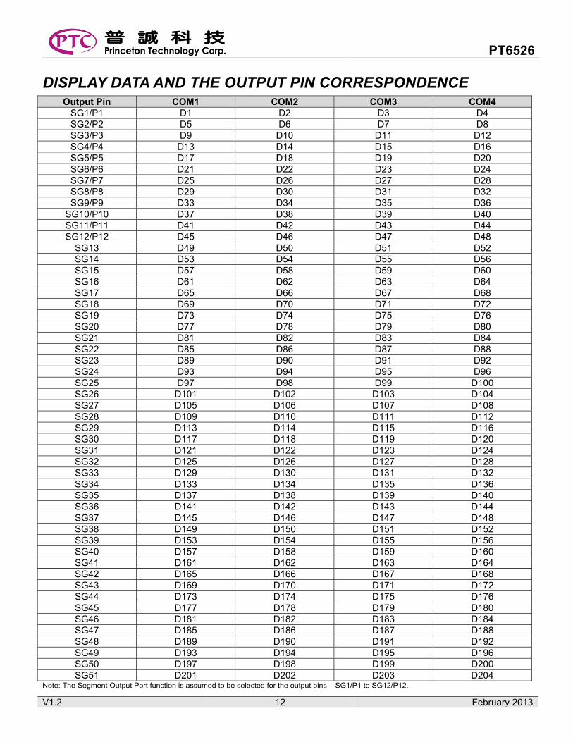
DISPLAY DATA AND THE OUTPUT PIN CORRESPONDENCE Output Pin COM1 COM2 COM3 COM4
SG1/P1 D1 D2 D3 D4 SG2/P2 D5 D6 D7 D8 SG3/P3 D9 D10 D11 D12 SG4/P4 D13 D14 D15 D16 SG5/P5 D17 D18 D19 D20 SG6/P6 D21 D22 D23 D24 SG7/P7 D25 D26 D27 D28 SG8/P8 D29 D30 D31 D32 SG9/P9 D33 D34 D35 D36
SG10/P10 D37 D38 D39 D40 SG11/P11 D41 D42 D43 D44 SG12/P12 D45 D46 D47 D48
SG13 D49 D50 D51 D52 SG14 D53 D54 D55 D56 SG15 D57 D58 D59 D60 SG16 D61 D62 D63 D64 SG17 D65 D66 D67 D68 SG18 D69 D70 D71 D72 SG19 D73 D74 D75 D76 SG20 D77 D78 D79 D80 SG21 D81 D82 D83 D84 SG22 D85 D86 D87 D88 SG23 D89 D90 D91 D92 SG24 D93 D94 D95 D96 SG25 D97 D98 D99 D100 SG26 D101 D102 D103 D104 SG27 D105 D106 D107 D108 SG28 D109 D110 D111 D112 SG29 D113 D114 D115 D116 SG30 D117 D118 D119 D120 SG31 D121 D122 D123 D124 SG32 D125 D126 D127 D128 SG33 D129 D130 D131 D132 SG34 D133 D134 D135 D136 SG35 D137 D138 D139 D140 SG36 D141 D142 D143 D144 SG37 D145 D146 D147 D148 SG38 D149 D150 D151 D152 SG39 D153 D154 D155 D156 SG40 D157 D158 D159 D160 SG41 D161 D162 D163 D164 SG42 D165 D166 D167 D168 SG43 D169 D170 D171 D172 SG44 D173 D174 D175 D176 SG45 D177 D178 D179 D180 SG46 D181 D182 D183 D184 SG47 D185 D186 D187 D188 SG48 D189 D190 D191 D192 SG49 D193 D194 D195 D196 SG50 D197 D198 D199 D200 SG51 D201 D202 D203 D204
Note: The Segment Output Port function is assumed to be selected for the output pins – SG1/P1 to SG12/P12.

PT6526
V1.2 13 February 2013
To illustrate further, the states of the S21 output pin is given in the table below. Display Data
State of SG21 Output Pin D81 D82 D83 D84
0 0 0 0 LCD Segments corresponding to COM1 to COM4 are OFF. 0 0 0 1 LCD Segment corresponding to COM4 is ON. 0 0 1 0 LCD Segment corresponding to COM3 is ON. 0 0 1 1 LCD Segments corresponding to COM3 and COM4 are ON. 0 1 0 0 LCD Segment corresponding to COM2 is ON. 0 1 0 1 LCD Segments corresponding to COM2 and COM4 are ON. 0 1 1 0 LCD Segments corresponding to COM2 and COM3 are ON. 0 1 1 1 LCD Segments corresponding to COM2, COM3 and COM4 are ON. 1 0 0 0 LCD Segment corresponding to COM1 is ON. 1 0 0 1 LCD Segments corresponding to COM1 and COM4 are ON. 1 0 1 0 LCD Segments corresponding to COM1 and COM3 are ON. 1 0 1 1 LCD Segments corresponding to COM1, COM3 and COM4 are ON. 1 1 0 0 LCD Segments corresponding to COM1 and COM2 are ON. 1 1 0 1 LCD Segments corresponding to COM1, COM2, and COM4 are ON. 1 1 1 0 LCD Segments corresponding to COM1, COM2, and COM3 are ON. 1 1 1 1 LCD Segments corresponding to COM1 and COM 4 are ON.
PT6526
V1.2 14 February 2013
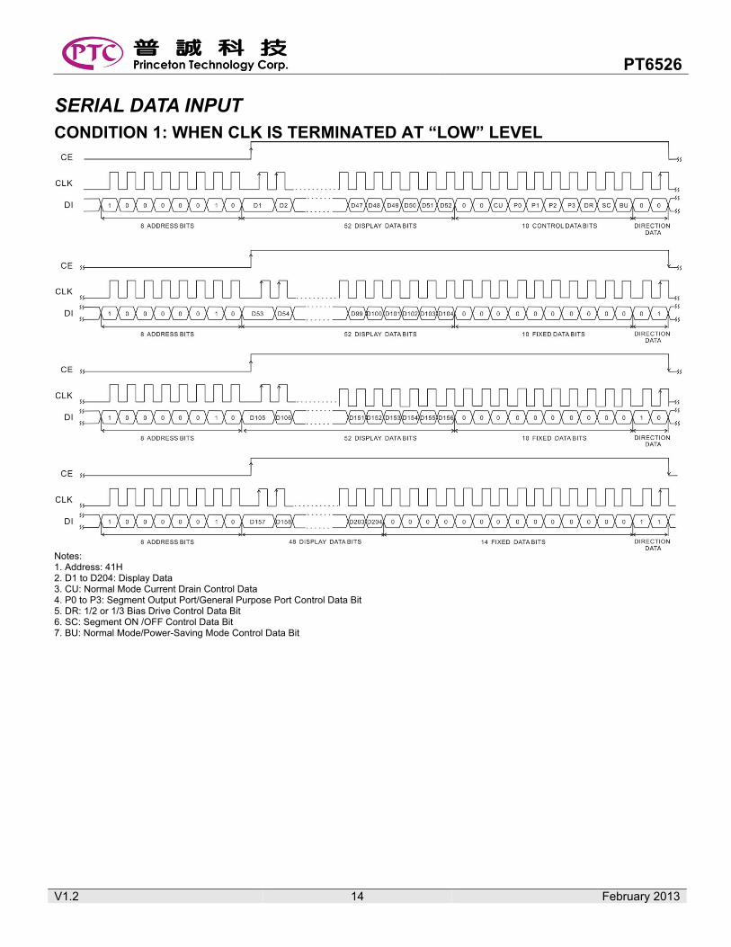
SERIAL DATA INPUT CONDITION 1: WHEN CLK IS TERMINATED AT “LOW” LEVEL
Notes: 1. Address: 41H 2. D1 to D204: Display Data 3. CU: Normal Mode Current Drain Control Data 4. P0 to P3: Segment Output Port/General Purpose Port Control Data Bit 5. DR: 1/2 or 1/3 Bias Drive Control Data Bit 6. SC: Segment ON /OFF Control Data Bit 7. BU: Normal Mode/Power-Saving Mode Control Data Bit

PT6526
V1.2 15 February 2013
CONDITION 2: WHEN CLK IS TERMINATED AT “HIGH” LEVEL
Notes: 1. Address: 41H 2. D1 to D204: Display Data 3. CU: Normal Mode Current Drain Control Data 4. P0 to P3: Segment Output Port / General Purpose Port Control Data Bit 5. DR: 1/2 or 1/3 Bias Drive Control Data Bit 6. SC: Segment ON /OFF Control Data Bit 7. BU: Normal Mode/Power-Saving Mode Control Data Bit

PT6526
V1.2 16 February 2013
SERIAL DATA TRANSFER SERIAL DATA TRANSFER FOR 157 OR MORE SEGMENTS
SERIAL DATA TRANSFER FOR LESS THAN 157 SEGMENTS Under a serial data transfer whereby less than 157 segments are used, 64, 128 or 192 bits of serial data must be transmitted depending on the actual number of segments used. The display data bits D1 to D52 and the control data must always sent. Please refer to the figure below.

PT6526
V1.2 17 February 2013
1/4 DUTY, 1/2 BIAS DRIVE TECHNIQUE

PT6526
V1.2 18 February 2013
1/4 DUTY, 1/3 BIAS DRIVE TECHNIQUE

PT6526
V1.2 19 February 2013
ABSOLUTE MAXIMUM RATING (Unless otherwise stated, Ta=25oC, Vss=0V)
Parameter Symbol Condition Rating Unit Maximum Supply Voltage VDDmax VDD -0.3 to +7.0 V
Input Voltage VIN1 CE, CLK, DI, /INH -0.3 to +7.0 V VIN2 OSC, VDD1, VDD2 -0.3 to VDD+0.3 V
Output Voltage VOUT OSC, SG1 to SG51,
COM1 to COM4, P1 to P12 -0.3 to VDD+0.3 V
Output Current IOUT1 SG1 to SG51 300 µA IOUT2 COM1 to COM4 3 mA IOUT3 P1 to P12 5 mA
Allowable Power Dissipation PDmax Ta=85oC 200 mW Operating Temperature Topr -40 to +85 oCStorage Temperature Tstg -40 to +150 oC
ALLOWABLE OPERATING RANGE (Unless otherwise stated, Ta=25oC, Vss=0V)
Parameter Symbol Condition Min. Typ. Max. Unit Supply Voltage VDD VDD 4.5 - 6.0 V
Input Voltage VDD1 VDD1 - 2/3VDD VDD V VDD2 VDD2 - 1/3VDD VDD V
High Level Input Voltage VIH CE, CLK, DI, /INH 2.4 - VDD V Low Level Input Voltage VIL CE, CLK, DI, /INH 0 - 0.7 V Recommended External Resistance
Rosc OSC - 270 - KΩ
Recommended External Capacitance
Cosc OSC - 100 - pF
Guaranteed Oscillation Range
fosc OSC 25 50 100 KHz
Data Setup Time tds CLK, DI (see Note) 160 - - ns Data Hold Time tdh CLK, DI (see Note) 160 - - ns CE Wait Time tcp CE, CLK (see Note) 160 - - ns CE Setup Time tcs CE, CLK (see Note) 160 - - ns CE Hold Time tch CE, CLK (see Note) 160 - - ns High Level Clock Pulse Width tΦH CLK (see Note) 160 - - ns
Low Level Clock Pulse Width tΦL CLK, (see Note) 160 - - ns
Rise Time tr CE, CLK, DI (see Note) - 160 - ns Fall Time tf CE, CLK, DI (see Note) - 160 - ns /INH Switching Time tc /INH, CE (see Note) 10 - - µs

PT6526
V1.2 20 February 2013
Notes: 1. When CLK is terminated at “LOW” level
2. When CLK is terminated at “HIGH” level.

PT6526
V1.2 21 February 2013
ELECTRICAL CHARACTERISTICS (Unless otherwise stated, Ta=25oC, Vss=0V)
Parameter Symbol Conditions Min. Typ. Max. UnitHysteresis VH CE, CLK, DI, /INH - 0.1VDD - V High Level Input Current
IIH CE, CLK, DI, /INH
VI=6.0V - - 5.0 µA
Low Level Input Current
IIL CE, CLK, DI, /INH
VI=0V -5.0 - - µA
High Level Output Voltage
VOH1 SG1 to SG51
Io=-20µA VDD-1.0 - - V
VOH2 COM1 to COM2
Io=-100µA VDD-1.0 - -
V
VOH3 P1 to P12 Io=-1mA
VDD-1.0 - - V
Low Level Output Voltage
VOL1 SG1 to SG51
Io=20µA - - 1.0 V
VOL2 COM1 to COM4
Io=100µA - - 1.0 V
VOL3 P1 to P12 Io=1mA
- - 1.0 V
Middle Level Output Voltage
VMID1 COM1 to COM4
1/2 Bias, Io=±100µA 1/2VDD-1.0 - 1/2VDD+1.0 V
VMID2 SG1 to SG51
1/3 Bias, Io=±20µA 2/3VDD-1.0 - 2/3VDD+1.0 V
VMID3 SG1 to SG51
1/3 Bias, Io=±20µA 1/3VDD-1.0 - 1/3VDD+1.0 V
VMID4 COM1 to COM4
1/3 Bias, Io=±100µA 2/3VDD-1.0 - 2/3VDD+1.0 V
VMID5 COM1 to COM4
1/3 Bias, Io=±100µA 1/3VDD-1.0 - 1/3VDD+1.0 V
Oscillation Fequency Fosc OSC
Rosc=270KΩ, Cosc=100pF 40 50 60 KHz
Current Drain
IDD1 Power Saving Mode - - 5 µA
IDD2
VDD=6V Outputs Open
1/2 Bias, fosc=50KHZ Control Data CU=0
- 200 400 µA
IDD3
VDD=6.0V Outputs Open
1/3 Bias, fosc=50KHz Control Data CU=0
- 250 500 µA
IDD4
VDD=6.0V Outputs Open
1/2 Bias, fosc=50KHz Control Data CU=1
- 130 260 µA
IDD5
VDD=6.0 Outputs Open
1/3 Bias, fosc=50KHz Control Data CU=1
- 150 300 µA
PT6526
V1.2 22 February 2013
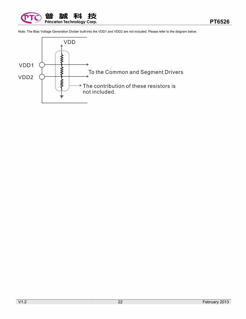
Note: The Bias Voltage Generation Divider built-into the VDD1 and VDD2 are not included. Please refer to the diagram below.

PT6526
V1.2 23 February 2013
PACKAGE INFORMATION 64-PIN, LQFP (BODY SIZE: 10mm x 10mm, PITCH: 0.50mm, THK BODY: 1.40mm)
Symbol Min. Nom. Max.
A - - 1.60
A1 0.05 - 0.15
A2 1.35 1.40 1.45
b 0.17 0.22 0.27
c 0.09 - 0.20
D 11.80 12.00 12.20
D1 9.90 10.00 10.10
E 11.80 12.00 12.20
E1 9.90 10.00 10.10
e 0.50 BSC
L 0.45 0.60 0.75
L1 1.00 REF
θ 0° 3.5° 7°
Notes: 1. Unit: mm 2. Refer to JEDEC MS-026 BCB

PT6526
V1.2 24 February 2013
IMPORTANT NOTICE Princeton Technology Corporation (PTC) reserves the right to make corrections, modifications, enhancements, improvements, and other changes to its products and to discontinue any product without notice at any time. PTC cannot assume responsibility for use of any circuitry other than circuitry entirely embodied in a PTC product. No circuit patent licenses are implied. Princeton Technology Corp. 2F, 233-1, Baociao Road, Sindian Dist., New Taipei City 23145, Taiwan Tel: 886-2-66296288 Fax: 886-2-29174598 http://www.princeton.com.tw