design and development of high voltage regulated power
TRANSCRIPT

Design and development of high voltage regulated power converters based on advanced techniques
with suitable protection schemes and study on EMI characterization
By
SAJJAN KUMAR THAKUR
(Enrollment No: ENGG04201104003)
Variable Energy Cyclotron Centre Kolkata-700064, India
A thesis submitted to the Board of Studies in Engineering Sciences
in partial fulfillment of requirements for the Degree of
DOCTOR OF PHILOSOPHY
of
HOMI BHABHA NATIONAL INSTITUTE
June, 2018

Statement by author
ii

Statement by author
iii
STATEMENT BY AUTHOR
This dissertation has been submitted in partial fulfillment of requirements for an
advanced degree at Homi Bhabha National Institute (HBNI) and is deposited in the Library
to be made available to borrowers under rules of the HBNI.
Brief quotations from this dissertation are allowable without special permission,
provided that accurate acknowledgement of source is made. Requests for permission for
extended quotation from or reproduction of this manuscript in whole or in part may be
granted by the Competent Authority of HBNI when in his or her judgment the proposed
use of the material is in the interests of scholarship. In all other instances, however,
permission must be obtained from the author.
SAJJAN KUMAR THAKUR

Declaration
iv
DECLARATION
I, hereby declare that the investigation presented in the thesis has been carried out by
me. The work is original and has not been submitted earlier as a whole or in part for a
degree / diploma at this or any other Institution / University.
SAJJAN KUMAR THAKUR

v
List of Publications arising from the thesis
1. S. K. Thakur, “Design and performance of high voltage power supply with crowbar
protection for 3-
Journal Publications:-
Φ high power rf amplifier system of cyclotron”. Journal of
Instrumentation (JINST 11 T07004), vol.-11, 2016.
2. S. K. Thakur, S. Kumari, Yashwant Kumar, “Design and performance analysis of a
crowbar-less high voltage power supply based on PSM technique” Sadhana Journal,
vol-43, issue- 8, 2018, pp 1-9/129: 129.
https://www.ias.ac.in/article/fulltext/sadh/043/08/0129.
3. S. K. Thakur, Y. Kumar, “Design development and testing of high voltage power
supply with crowbar protection for IOT based RF amplifier system in VECC”. Journal
of Instrumentation (JINST 13 T05009), vol. –13, 2018.
1) S. K. Thakur, Santwana K. , A. De, Y. Kumar, V. Lilhare, A. Bera, S. S. Pal, V. K.
Khare, T. P. Tiwari, S. Saha. “Design and Development of Prototype High Voltage
Power Supply with PSM Technique for RF Amplifier”. InPAC-2013, Kolkata, 2013,
pp 570-572.
Conference Publications:
2) S. Srivastava, Yashwant Kumar, A. Misra, S.K. Thakur and V.S. Pandit. “Optimum
Design of Buck Converter Controller using LQR Approach”. IEEE International
Conference in Advance computing- 2013.

vi
3) Yashwant Kumar, S. Srivstava, A. Bera, T.P. Tiwari, H.K. Panday, S.K. Thakur, S.
Saha. “Design and development of switch mode power supply for 3.0 kW a Solid State
RF amplifier”, InPAC-2015, Mumbai.
1) De A.; Kumari S.; Khare V.K.; Pal S.S.; Sadhukhan A.; Meshram V.K.; Thakur S.K.;
Saha S. “Design Analysis and Implementation of a Dynamic Voltage Restorer “,
Journal of Low Power Electronics (JOLPE), Vol 9, No. 3, 2013, pp-340-349.
Other Publications :
2) Saurabh Srivastava, Anuraag Misra, S. K. Thakur, V. S. Pandit, “An optimal PID
controller via LQR for standard second order plus time delay systems”, ISA
Transactions, 60.(2016) 244-253.
3) V. S. Pandit, G. Pal, S. K. Thakur, P. Singh Babu, A. Goswami, Mou Chatterjee,
R.C.Yadav, S. Srivastava, S. Bhattacharya, S. Roy, C. Nandi, A Misra. “Microwave
ion source and injection system for a high current compact cyclotron”, 2nd
International Workshop on ADS & Thorium Utilization, December 11-14, 2011,
BARC Mumbai.
4) Anirban De, S.S. Pal, P. Bhaskar, S. Kumari, V.K. Khare, A. Duttaroy, M. Garai, S.K.
Thakur, S. Saha, Sankha Chattopadhyay, Luna Barua, Sujata Saha Das, U. Kumar,
M.K. Das. “An Embedded System based Computer Controlled Process Automation for
Recovery and Purification of 99mTc from (n,γ) 99Mo”, Proceeding of the 9th
International Workshop on Personal Computers and Particle Accelerator Controls
(PCaPAC2012), VECC, Kolkata, pp. 211-213, 4-7 Dec. 2012.
5) De A.; Kumari S.; Khare V.K.; Pal S.S.; Sadhukhan A.; Meshram V.K.; Thakur S.K.;
Saha S. “Design, Development and Testing of a DSP Based Dynamic Voltage
vii
Restorer”, Published in Electronic System Design (ISED), 2012 International
Symposium, pp.157-161, 19-22 Dec. 2012.
6) Bidhan Chandra Mandal, Uttam Bhunia, Javed Akhtar, Jedidiah Pradhan, Chinmay
Nandi, Sajjan Kumar Thakur, Manoranjan Das, Gautam Pal and Subimal Saha.
“Dynamic loss analysis for 4.5 MJ SMES”, Paper Presented in National Symposium
on Cryogenics (NSC-24) held during January, 2013 at IPR, Ahmedabad.
7) V.S. Pandit, P.Sing. Babu, A. Goswami, S. Srivasatava , A.Misra , Mou chatterjee,
P.Y.Nabhiraj, R.C.Yadav, S.Bhattacharya, S.Roy, C.Nandi, G.Pal, S.K.Thakur,
“Development of microwave ion source and low energy beam transport system for
high current compact cyclotron”, Paper presented in International conference on
electromagnetic isotope separators and related technologies (EMIS-2012), Matsue,
Japan.
8) H.K.Pandey, T. K. Mandi, Y. Kumar, D.P. Dutta, S. Basak, S.K. Thakur, K.P.Ray, A.
Bandopadhyay. “Design and development of 37.8 MHz, 2.0 kW RF amplifier for re
buncher of RIB project”. Paper published in InPAC-2013 held at VECC, Kolkata ,
2013, pp-624-626.
9) Yashwant kumar, Santwana Kumari, M. K. Ghosh, A. Bera, A. Sadhukhan, S. S. Pal,
V. K. Khare, T. P. Tiwari, S. K. Thakur, S. Saha. “Design and Development of Power
Supplies for High Power IOT based RF Amplifier”. Paper published in InPAC-2013
held at VECC, Kolkata, 2013, pp. 500-502.
10) Saurabh Srivastava, Yashwant Kumar, Anuraag Misra, Vijay Shanker Pandit, Sajjan
Kumar Thakur. “A Control Strategy for Highly Regulated Magnet Power Supplies
Using a LQR Approach” Paper presented in ICALEPCS -2013.

viii
11) J Pradhan, Nisith Kr Das, Anindya Roy, Uttam Bhunia,Vipendra Khare, Sajjan
Kumar Thakur and S. Saha. “Design and Development of Cryogen Free Cryogenic
Test set-up”. 26th International Cryogenic Engineering & International Cryogenic
Material Conference (ICEC26-ICMC-16), New Delhi, 2016.
12) U Bhunia, J Pradhan, A Roy, V K Khare, M K Dey, S K Thakur, H Kanithi.
“Transient stability of NbTi Rutherford cables for energy storage magnet
applications”. 26th International Cryogenic Engineering & International Cryogenic
Material Conference (ICEC26-ICMC-16), New Delhi, 2016.
13) V. K. Khare, U. Bhunia, A. De, J. Pradhan, S. K. Thakur, M. Das, S. Saha. “Joint
development and testing of Rutherford NbTi cable for SMES coil”. 26th International
Cryogenic Engineering & International Cryogenic Material Conference (ICEC26-
ICMC-16), New Delhi, 2016.
14) Md. Zamal Abdul Naser, Siddhartha Dechoudhury, Manas Mondal, A. Polley, H.K.
Pandey, D.P. Dutta, S.K. Thakur, Arup Bandyopadhyay, Vaishali Naik and Alok
Chakrabarti. “Present status of design, installation and testing of electron gun and low
energy beam transport line of electron linac at VECC”. InPAC-2015, held during
December 21-24, 2015 in Mumbai.
SAJJAN KUMAR THAKUR

ix
Dedicated to my parents
Shri K. N. Thakur and Smt. Mira Thakur.

Acknowledgements
x
ACKNOWLEDGEMENTS
I express my sincere gratitude to my guide Dr. Alok Chakrabarti for the valuable
guidance and encouragement to my PhD works. I am greatly indebted and respectful to Dr.
V. S. Pandit for his guidance and continuous encouragement throughout my thesis work,
without whose support, my thesis could not have been possible to come to the concluding
stage. I would like to express my heartfelt thanks to Dr. D. K. Srivastava, Former-Director,
VECC and Chairman of my PhD committee for his kind support and encouragement. I take
the opportunity to thank Dr. Sumit Som, Head, ATG for the technical guidance and
encouragement throughout the work during development and testing of the High Voltage
power supplies with RF systems.
I express my sincere gratitude to Dr. R. K. Bhandari, Former-Director, VECC who
has granted me the permission to carry out my PhD work in the field of High Voltage. I
take this opportunity to thank Shri Subimal Saha, Ex-Head, Accelerator Technology Group
for providing me the opportunity to work on high voltage power systems for RF Amplifiers
for the cyclotrons. I would like to thank my PhD committee members Dr. Sandip Sarkar,
SINP for his valuable suggestions and encouragements. I am sincerely thankful to Dr.
Paramita Mukherjee, former Dean, HBNI, Kolkata for her continuous supports,
encouragements and valuable suggestions throughout my PhD work.
I would like to express my sincere thanks to each and every staff members of
PE&MCD section for their technical supports all the time during the development and
testing of high voltage power systems which are very dangerous and critical in nature. My
sincere thanks to my colleagues Shri Saurabh Srivastava, Shri Yashwant Kumar, Smt.
Santwana Kumari, Dr. Anuraag Misra, Dr. Anirban De, Shri T P Tiwari, Shri J. S. Prasad,

Acknowledgements
xi
Shri SS Pal and each and everybody from PE&MCD section and RF Section for their
continuous supports without which it would not be so easy to achieve the goal.
I am very much thankful to my wife Lina for her consistent motivation,
encouragement, support and self-sacrifice during my PhD work. I am thankful to my son
Rohan for keeping my mind refreshed by enjoying the precious days of his childhood with
him. I am eternally grateful to my parents and parents-in-law for everything what they have
done for me in my life. Above all, I owe it all to Almighty God for granting me the
wisdom, health and strength to undertake this research task and enabling me to its
completion.
SAJJAN KUMAR THAKUR
Table of contents
xii
Table of Contents
Synopsis ................................................................................................................................. 1
List of Figures ....................................................................................................................... 8
List of Tables ...................................................................................................................... 11
List of Abbreviations ......................................................................................................... 12
1. Introduction .................................................................................................................... 14
1.1 Background ........................................................................................................... 14 1.2 Power converter topologies: switching and PSM .................................................. 16 1.3 Research motivation .............................................................................................. 21 1.4 Contribution of the thesis ...................................................................................... 22 1.5 Outline of the thesis ............................................................................................... 23
2. Design and development of high voltage power supply for K-500 SC cyclotron high
power rf amplifier with crowbar protection. ................................................................... 27
2.1 Introduction ........................................................................................................... 27 2.2 Different power supplies for high power rf amplifier ........................................... 30
2.2.1 Anode power supply ....................................................................................... 30
2.2.2 Screen power supply ....................................................................................... 35
2.2.3 Grid power supply .......................................................................................... 36
2.2.4 Filament power supply .................................................................................... 37
2.3 Crowbar protection system .................................................................................... 37 2.3.1 Crowbar circuit block diagram ....................................................................... 38
2.3.2 Timing calculation .......................................................................................... 40
2.3.3 Test setup and wire selection .......................................................................... 42
2.4 Data acquisition ..................................................................................................... 44 2.4.1 Interlocks and sequence of instruction ............................................................ 45
2.5 Test results and discussion .................................................................................... 46

Table of contents
xiii
2.6 Summary and conclusion ...................................................................................... 48
3. High voltage power supply (-30 kV, 3.2 A) with crowbar protection for Inductive
Output Tube based rf amplifier system ........................................................................... 50
3.1 Introduction ........................................................................................................... 50 3.2 Block diagram of IOT based rf amplifier .............................................................. 52
3.2.1 High voltage deck ........................................................................................... 53
3.3 HV power supply (-30 kV, 3.2 A) ......................................................................... 54 3.4 Other power supplies for IOT ............................................................................... 59 3.5 Supervisory control and monitoring ...................................................................... 59 3.6 Crowbar system for IOT based amplifier .............................................................. 60
3.6.1 Wire survivability test ..................................................................................... 64
3.7 Experimental results and discussion ...................................................................... 64 3.8 Summary ............................................................................................................... 67
4. Crowbar less high voltage power supply rated at -40 kV, 5 A based on pulse step
modulation (PSM) technique ............................................................................................ 68
4.1 Introduction ........................................................................................................... 68 4.2 HVPS description .................................................................................................. 70
4.2.1 Scheme of HVPS of rating -40 kV, 5 A ......................................................... 70
4.2.2 Multi secondary transformers ......................................................................... 72
4.2.3 Switched power modules (SPM) .................................................................... 74
4.3 Control scheme of PSM based HVPS ................................................................... 76 4.3.1 Working principle of PSM .............................................................................. 76
4.3.2 Closed loop control program .......................................................................... 79
4.3.3 Supervisory control and monitoring ............................................................... 83
4.4 Results and discussion ........................................................................................... 84 4.5 Summary and conclusion ...................................................................................... 86
5. Study on harmonics and EMI ....................................................................................... 87
5.1 Introduction ........................................................................................................... 87 5.2 Study on harmonics and their analysis .................................................................. 88
5.2.1 Fourier Series .................................................................................................. 91
5.2.2 Harmonics reduction by transformer configuration ........................................ 92

Table of contents
xiv
5.2.3 Harmonics standards ....................................................................................... 94
5.3 Study on EMI and EMC ........................................................................................ 94 5.3.1 EMI characterisation ....................................................................................... 97
5.3.2 EMC standards ................................................................................................ 99
6. Conclusion and future works ...................................................................................... 102
6.1 Conclusion ........................................................................................................... 102 6.2 Future works ........................................................................................................ 104
Bibliography .................................................................................................................... 105

Synopsis
1
Synopsis The work presented in the thesis deals with the development of a number of high
voltage power converters / supplies, viz. 20 kV, 22.5 A; -30 kV, 3.2 A; -40 kV; 5 A for the
K 500 Superconducting Cyclotron and other project at VECC, Kolkata. In the present
dissertation, several topologies, e.g., switching type, high voltage tetrode tube based linear
regulator type, primary phase angle controlled by using SCRs were studied for the
development of high voltage power converters for the cyclotrons at VECC. Subsequently,
their design and development was carried out and then the converters were coupled to the
cyclotrons at VECC. Their performances have been satisfactory even after 6 years of
continuous operation. The performances of the conventional power supplies are required to
be improved as demanded from load end which is carried out by adopting PSM topology as
being a latest and emerging technique. Generally, the conventional power converters are
larger in size and contain high stored energy. Hence, rf tubes need to be protected against
excessive energy dissipation during internal arc fault for which a crowbar protection
system is required to be implemented. However, in PSM based high voltage power
converters, no additional device is necessary for the crowbar protection. This is because the
PSM technique uses high frequency switching in each power module which requires very
low capacitors and results in very small stored energy. A Digital Signal Processor (DSP)
based controller is developed indigenously which has less susceptibility to environmental
noise that results better regulation, stability and control.
The design and development of these high voltage power supplies (HVPS) require
lots of efforts for (i) finalizing the appropriate topologies to meet the requirements, (ii)
design of appropriate control architecture, (iii) design of HVPS based on available

Synopsis
2
components including interlocks and protection system and finally (iv) completely new
development of a HVPS of rating -40 kV, 5 A using PSM technique which would allow us
to meet the design goals in a much more efficient and safe way. It may be mentioned that
many of these converters could have been commercially procured but the prohibitive cost,
the long term maintenance issues and minimizing of machine down time are the factors that
have led to the decision to develop the new technology. In absence of enough detailed
literatures on these converters, the developments become an intensive R&D which involves
detailed study, work out of the design, prototype fabrication before finalizing the actual
unit of power supply and finally the development, testing and commissioning of the high
voltage power supply. Further, we believe that these developments have certain unique
aspects that are novel in the sense those were done differently in the commercially
available converters.
The present thesis consists of six chapters whose main contents are described below.
Chapter-1 is the introduction that contains discussion on various aspects of the high
voltage regulated power supplies along with their control. The needs for the improvements
as demanded by the various applications are worked out which created the motivation for
the present research work. A part of the chapter is also dedicated to literature survey that
brings out the present state of the art development in this field.
Chapter-2 contains the detailed description of design, fabrication and testing of a
high voltage power supply rated at 20 kV, 22.5 A (output power 450 kW) along with
ultrafast crowbar protection system. The Radio Frequency system of K 500
Superconducting Cyclotron (SCC) at VECC consists of 3 nos. of rf cavities (dee) separated
at 120o apart in the median plane. Each cavity is designed for 80 kW rf power to produce

Synopsis
3
dee voltage of 100 kV in the operating frequency range of 9-27 MHz. To produce such a
high voltage, each cavity requires individual tetrode tube (Eimac 4CW150,000E) based rf
amplifier.
The power supply rated at 20 kV, 22.5 A has been being used to feed power to the
anodes of all three tetrode tubes based rf amplifiers for K 500 superconducting cyclotron
(SCC) at VECC campus. All the three tetrode tubes are protected by a single ignitron based
crowbar protection system against internal arcing fault in any of the tubes. The tubes are
very much prone to undergo internal arcing and energy deposition in the tube during
internal arcing must be restricted to the value specified by the manufacturers. In order to
minimize the deposition of energy, a very specialized technique is adopted that diverts the
energy through an ignitron followed by tripping the input power. A technique has been
designed for fast sensing of the arc current and initiating the triggering of a high voltage
ignitron within 5 μs in order to limit the energy deposition which is called crowbar
protection. The wire burn test was performed for confirmatory test of the crowbar
protection system, a special technique to simulate the actual deposition of stored energy.
This chapter presents the salient design features, simulation, in-house development and
technical challenges during the testing of the high voltage anode power supply and crowbar
protection system for the rf amplifier tubes.
Each tetrode tube requires individual dc power supplies for biasing its electrodes:
anode, screen, grid and filament with respect to grounded cathode. All these power supplies
are designed, fabricated and tested along with Local & Remote controls, ON/OFF
sequencing together with the interlocks & protection. The ratings of the power supplies are:
filament power supply 16 V, 220 A, grid power supply -500 V, 0.1 A with 100 ppm

Synopsis
4
stability, screen power supply 1600 V, 500 mA with 60 ppm stability and a high voltage
anode power supply rated at 20 kV, 22 A for the anodes of three tubes.
In Chapter 3, the development of a negative polarity high voltage power supply (-30
kV, 3.2 A) required for biasing the electrodes of Inductive output tube (IOT) based rf
amplifier test stand working at 700 MHz in continuous mode has been presented.
The development of multi-cell (5 cell) medium-β Superconducting rf linac cavity has
been taken up at Variable Energy Cyclotron Centre (VECC), Kolkata, as a part of Indian
Institutes - Fermi Lab, USA collaboration. For this the design and development of a high
power (~60 kW at 700 MHz in CW mode) rf amplifier has been taken up based on
Inductive Output Tube (IOT). For this, a set of dc power supplies for biasing the IOT has
been developed, installed and tested.
High voltage power supply (HVPS) of rating -30 kV, 3.2 A is designed and developed
for biasing IOT Cathode. A back to back primary SCR based phase angle controlled
topology is utilised for voltage regulation. The crowbar protection system is implemented
which is more complex in negative polarity power converter. The complicacy in
implementing the crowbar protection by using ignitron (NL7703) is also addressed with the
solution. Testing of the crowbar system is done by using wire burn method. Other auxiliary
power supplies are used for grid, filament, ion pump, focus coil. The power supplies for
grid, filament and ion pump of IOT are with respect to the cathode which is floating at high
voltage. So, these power supplies are placed at a high voltage deck and parameters control
and monitoring are done through a PLC based system. A high voltage deck is specially
designed by using insulating material with metallic enclosure having isolation ~40 kV to
house these power supplies. The electrical power is fed through an Isolation Transformer of

Synopsis
5
isolation 40 kV. These power supplies are controlled by a PLC, which communicates
through an Optical Fibre link to the PC.
Chapter 4 is dedicated mainly to the development of a high voltage power supply
based on state of the art pulse step modulation (PSM) technique for ~60 kW continuous
wave (cw) rf amplifier based on Inductive output tube (IOT) TH793-1 operating at 700
MHz. For a nominal beam bias, cathode requires a high voltage power supply (HVPS) of
rating -40 kV, 5 A is considered for design and development. The present development is
aimed to utilise a modern technique meeting all the important criteria, i.e., solid state based
modular construction, small size, crowbar-less design, reliable operation, voltage regulation
with higher efficiency, fast response and most importantly easy servicing. In this chapter,
the design details and test results of high voltage power supply (HVPS) by using DSP
TMS320F28335 as the main controller has been presented.
Inductive output tube (IOT), a hybrid of klystron and triode, has advantages in term
of better linearity and efficiency over klystron and in terms of gain over tetrode tube. IOT
requires several power supplies for biasing its electrodes. High voltage power supply for
cathode is one of the important which should have voltage regulation better than 0.5% and
low ripple. The high voltage power converter (rating -40 kV, 5 A) is designed and
developed by using Pulse Switch Modulation (PSM) topology, a latest technique required
to fulfil most of the designed features. PSM based high voltage power supply consists of
several switched type power modules (SPMs) and the output voltage is obtained by adding
the output voltages of each SPMs in series and modulating their pulse widths and phase
delay time. This results into very low ripple voltage at higher frequency which ultimately

Synopsis
6
requires very small filter capacitor resulting into very low stored energy. Thus PSM based
power supply does not require a separate crowbar protection system.
The high voltage power supply (HVPS) consists of 60 switched power modules
(SPMs) and two resin cast air cooled multi-secondary transformers, each having 30
secondaries star-connected, 3-phase, line voltage 580 V, 50 Hz to power each SPM
individually. The primary connection of one transformer is delta and other is star for
providing 12 pulse rectification features when both transformers power equal SPMs. Solid
state based SPM uses an IGBT in series as a buck converter with a typical output voltage of
around 780 V at a fixed duty cycle of 80% at switching frequency 5 kHz. The operation
involves switching-on the required number of SPMs till a set value of output voltage is
arrived. The output voltage finer setting and regulation is accomplished by pulse width
modulation (PWM) of 2 SPMs with variable dc voltage. A DSP based control system is
developed in order to ensure the trouble free operation of the power supply as well as
option for future upgrade without much change in hardware.
For biasing an IOT, auxiliary power supplies for filament, grid and ion-pump are
needed with respect to cathode which are kept at high voltage deck at 50 kV isolation and
powered by a resin cast isolation transformer of isolation voltage ~50 kV. Two Ethernet
optical fibre media converters connected to a PLC through 5 m long optical fibre link for
their controls and communications. Focus coil power supply is with respect to the ground
level so, it is easy to control.
Chapter 5 describes the study on harmonics and EMI, their basic concepts of
generation and side effects. Electromagnetic interference (EMI) becomes a major concern
for high power SMPS power supplies and various types of motor drives in electrical field.

Synopsis
7
It causes conducted and radiated EMI noise which creates nuisance for other electronic
equipment. Electromagnetic compatibility (EMC) is the ability of any electronics systems
to function without causing or experiencing performance degradation due to EMI produced
nearby.
Chapter 6 contains the conclusions and perspective of high voltage related work to
be carried out at VECC in future.

List of Figures
8
List of Figures Figure 1-1: Schematic diagram of Buck type switching regulator ...................................... 17
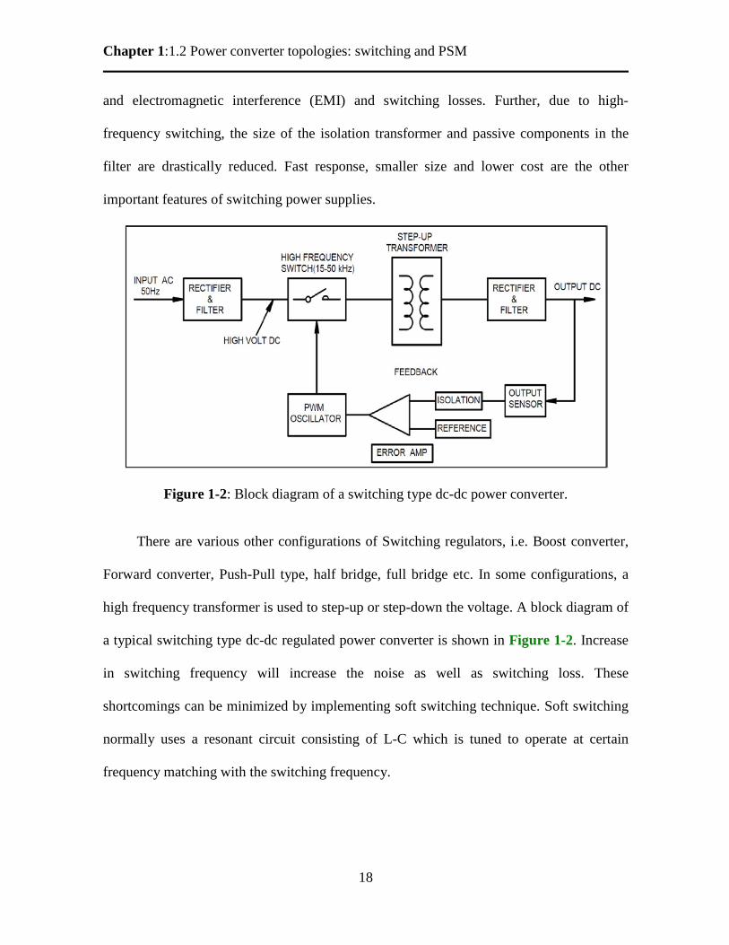
Figure 1-2: Block diagram of a switching type dc-dc power converter. ............................. 18
Figure 1-3 : dc-dc power converter with soft switching scheme ........................................ 19
Figure 2-1: Schematic layout of locations of different power supplies and rf amplifiers
used in the K-500 Cyclotron building .................................................................................. 29
Figure 2-2: Schematic diagram of anode power supply with ignitron and a tube. ............. 31
Figure 2-3: Photograph shows the local main control panel with monitoring and fault
indications for all the power supplies and two transformers of anode power supply. ......... 32
Figure 2-4: (a) Schematic diagram of crowbar protection system (b) Simulation result of
the crowbar protection system of anode power supply. ....................................................... 35
Figure 2-5: Schematic diagram of screen power supplies for the rf amplifiers. ................. 36
Figure 2-6: Schematic of scheme of crowbar protection system. ....................................... 40
Figure 2-7: Graph showing the calculated length with respect to wire gauge for a fixed
fusing energy. ....................................................................................................................... 43
Figure 2-8: RF system control and monitor GUI. .............................................................. 45
Figure 2-9: Ch-1- A 24V voltage is applied corresponding to a simulated fault (20 V/div),
Ch-2- Pulse transformer output showing 2.8 kV pulse at rise time 1.5 μs (500 V/div). Time
scale 1 µs/div. ....................................................................................................................... 46
Figure 2-10: Ch-1(top)- output voltage at 18 kV (10 kV/div), Ch-2 (middle)- current flows
through wire by using a CT (100 A/div), Ch-4 (bottom)- signal for tripping the CBs
simultaneous to the ignitron trigger pulse. Time scale 1 μs/div. ......................................... 47
Figure 3-1: Scheme of IOT based rf system with all the power supplies and PLC. ........... 52

List of Figures
9
Figure 3-2: Photographs of (A) high voltage deck consisting of three power supplies and
isolation transformer (B) PLC based control system. .......................................................... 53
Figure 3-3: Schematic diagram of HVPS (-30 kV/3.2 A) along with crowbar protection. 55
Figure 3-4: Simulation schematic for cathode power supply. ............................................. 56
Figure 3-5: Simulation result shows in (A) improvement of power factor (B) the reduction
of input side current during short circuit condition and in (C) output ripple rejection. ....... 56
Figure 3-6: Scheme of crowbar protection system ............................................................. 60
Figure 3-7: Electronic circuit that senses and trigger crowbar ............................................ 63
Figure 3-8: HVPS in 3 cabinets, cabinet-1 consists of two CBs for Transformers, SCRs,
control cards and panels. Cabinet-2 consists of Transformers, six air-core chokes, rectifier
assemblies. Cabinet-3 filter capacitor and crowbar unit consisting of ignitron assembly,
water cooling etc. ................................................................................................................. 65
Figure 3-9 : (a) Ch-1-The moment fault was created (5V/div), Ch-2- Pulse transformer
output pulse of 2.5 kV having rise time 4μs (500 V/div). (b) Ch-1- shows the current
profile at 200 A/div and ch-2 shows the output voltage at 15 kV/div by using a potential
divider. ................................................................................................................................. 66
Figure 4-1: Schematic diagram of HVPS rated at -40 kV, 5 A. .......................................... 71
Figure 4-2: HVPS showing all 60 SPMs and two resin-cast transformers rear side. .......... 71
Figure 4-3: Actual photograph of a multi-secondary transformer, having overall dimension
(1700x650) mm, H= 1600mm. ............................................................................................ 73
Figure 4-4: Schematic diagram of a SPM ........................................................................... 74
Figure 4-5: Working principle of PSM based HVPS. ......................................................... 77
Figure 4-6: Output voltage waveform with shifted PWM for 4 SPMs ............................... 78

List of Figures
10
Figure 4-7 : TMS320F28335 with PWM output and Analog input ................................... 80
Figure 4-8: Block diagram of DSP based HVPS control architecture ................................ 81
Figure 4-9: Flow diagram of control architecture ............................................................... 82
Figure 4-10: HVPS control and monitor GUI. .................................................................... 83
Figure 4-11: Rise time and fall time of output voltage (10 kV/div) at 40 kV at no load. ... 84
Figure 4-12: Short circuit test (CH3: voltage 15 kV/div which is scaled down to 3:1 by
using voltage divider; CH1: current, 20 A/div) ................................................................... 85
Figure 5-1: A typical soft charging at 440 V (CH1- DC link voltage (yellow), CH2- Input
current (green)) which shows soft start condition of a transformer showing the soft
charging of capacitor filter in time interval of 6 s. ............................................................... 87
Figure 5-2: Input line current distorted waveform which contains harmonics. ................. 89
Figure 5-3: Complex waveform formed by adding the waveforms of several frequencies. 90
Figure 5-4: Primary transformer connection and analysis of transformers ........................ 93
Figure 5-5: Common Mode (CM) and Differential Mode (DM) Current ........................... 96
Figure 5-6: EMI Filter between switched power module and mains supply ...................... 97
Figure 5-7: Arrangement of conducted noise measurement by using LISN ....................... 99
Figure 5-8: A typical noise curve whose amplitude is plotted in frequency band [67] .... 100

List of Tables
11
List of Tables Table 2-1: - Components details and test results of the anode power supply ..................... 34
Table 2-2: Crowbar circuit specification ............................................................................. 39
Table 3-1: Specifications of high voltage power supply for IOT cathode .......................... 58
Table 4-1: Specifications of HVPS based on IOT requirement .......................................... 72

Abbreviations
12
List of Abbreviations SMPS Switching Mode Power Supply
PWM Pulse Width Modulation
CCM Continuous Conduction Mode
DCM Discontinuous Conduction Mode
PD Proportional Derivative
PFC Power Factor Correction
PI Proportional Integral
PID Proportional Integral Derivative
DCCT Direct Current, Current Transformer
IC Integrated Circuit
IGBT Insulated Gate Bipolar Transistor
EMI Electromagnetic Interference
rf Radio Frequency
PS Power Supply
PSM Pulse Switch Modulation
SPM Switched Power Module
EMI Electromagnetic Interference
EMC Electromagnetic Compatibility
ECR Electron Cyclotron Resonance
ZCS Zero Current Switching
ZVS Zero Voltage Switching
IOT Inductive Output Tube

Abbreviations
13
IGBT Insulated Gate Bipolar Transistor
ESP Electrostatic Precipitator
ADS Accelerator Driven Systems
RIB Radioactive Ion Beam
LCW Low Conductivity Water
HVPS High Voltage Power Supply
VECC Variable Energy Cyclotron Centre
Chapter 1:1.1 Background
14
CHAPTER 1
Introduction
1.1 Background
High voltage dc power converter (supply) is one of the key components for
electrostatics applications extensively used in the field of Accelerators, defense, consumer
markets and various industries. Industrial processes, for example, require significant
performances and operational conditions to enhance the productivity and to improve the
quality at reduced cost which prompted for further advancements with improved features.
In accelerators, the high voltage power supplies (HVPS) at high power are required for
various tubes i.e. Klystron, Tetrode tube, Inductive output Tube (IOT) based rf amplifiers.
These are primarily used to produce high electric field at radio frequency that is
synchronized with the speed of beam. Some other major applications of high voltage power
supplies involve capacitor charging, missile firing, fabric industries, ESP and many other
industrial applications.
The Variable Energy Cyclotron Centre at Kolkata is a premier institute for nuclear
science having excellent infrastructure for advanced research and development in
accelerator technology. Room temperature K 130 cyclotron was first indigenously
developed in India during 1977 and since then variety of activities have come up, such as,
extraction of heavy ion beam with external ECR, Medical Cyclotron, radioactive ion beam
(RIB) facility and many other activities related to material science ADS, detector etc.
Radioactive Beams (RIB) are indispensible tools for nuclear science to study structure of

Chapter 1:1.1 Background
15
unstable nuclie. Several components of RIB facility have already been tested and installed.
VECC is setting up a medical cyclotron to produce proton beam with energy up to 30 MeV
and current up to 350 µA to produce various isotopes for medical applications. The
cyclotron will also be used for R&D in material science and to settle the various problems
related with handling of high beam current on ADS related components. Apart from that,
VECC is also involved in the studies on using cyclotrons to achieve high power proton
beam, development of high current at low energy part of the accelerator to settle various
space charge related problems and R&D on superconducting cavities. With the vast
experience and expertise in accelerator technology, the challenging tasks of constructing
superconducting (SC) cyclotron and their different systems have been executed. This
cyclotron has already delivered internal beam and some modifications are underway to
achieve external beam. The SC cyclotron consists of assembly of various subsystems such
as cryogenics systems, magnets, rf system, ion source, injection and extraction system,
vacuum, control systems, beam transport, data processing systems etc. For the rf systems,
high power and high voltage power supplies are needed for producing high electric field at
very high frequency.
The power supplies are the major components for any sub-systems of accelerators,
i.e., rf system, main magnet, various other beam-line magnets and ECR. Performance and
beam quality of any accelerator depends on the quality of the power supplies. As the
advancement in the technology is going on, more and more accelerators are coming up and
accordingly the demand of high voltage power supplies with improved performance have
been also increased. Considering the high demands of custom built high voltage power

Chapter 1:1.1 Background
16
supplies, it was very important for in-house development so that any further improvement
in future can be easy to incorporate.
For high voltage dc power converter, switching technique is adopted mainly for
improved efficiency, faster response and good power management [1]. But on the other
hand, it produces noise which is very much vulnerable for most of the applications.
Switching at higher current produces more EMI and noise level and thus at much higher
power, the noise level could be a very serious issue. In order to minimize the noise level,
soft switching technique can be applied [2, 3]. But it has some limitations which may not
be very useful for a power supply of higher power. For very high power at high voltage,
Pulse-Step Modulation technique (PSM) can be adopted utilizing the switched type
modules. In this scheme, there are several modules of small power rating which are
switched at some fixed time delay between one to another and finally their output voltages
are connected in series to attain requisite voltage. A part of the work reported in the thesis
is on the design and development of a high voltage power supply rated at -40 kV, 5 A
based on PSM topology.
1.2 Power converter topologies: switching and PSM
Transformation of dc voltage from one level to other level is accomplished by a dc-
dc converter. There are various schemes of dc-dc converters which involve the
combination of power components along with control electronics for regulations and
protections. Linear type power converter has very specific range of applications due to its
inherent limitations in efficiency due to higher dissipation and non-availability of high
voltage components. On the other side, switching type converter topologies are widely used
in the dc power converters in various schemes [1] because of its inherent

Chapter 1:1.2 Power converter topologies: switching and PSM
17
advantages and faster response. The switch-mode operation results in low power
dissipation as it operates either in switch-on or switch-off mode. Due to switching at high
frequency, the filter capacitor requirements are greatly reduced which makes it very
compact and efficient. Each module is a buck type switching regulator used in PSM based
high voltage power supply.
Figure 1-1: Schematic diagram of buck type switching regulator
The configuration of buck type switching regulator is shown in Figure 1-1 where IGBT is
used as a regulating element and regulation is achieved by varying the duty cycle. In this
configuration, the output voltage is directly proportional to the duty cycle [1, 4].
dds
ont
t
t
ds
DVVTt
dtdtVT
Vs
on
on
==
+= ∫∫ 01
00
Where Vo denotes output voltage, D duty cycle and Vd is Input dc voltage.
However, these benefits of switching power supplies come at the cost of higher complexity
Chapter 1:1.2 Power converter topologies: switching and PSM
18
and electromagnetic interference (EMI) and switching losses. Further, due to high-
frequency switching, the size of the isolation transformer and passive components in the
filter are drastically reduced. Fast response, smaller size and lower cost are the other
important features of switching power supplies.
Figure 1-2: Block diagram of a switching type dc-dc power converter.
There are various other configurations of Switching regulators, i.e. Boost converter,
Forward converter, Push-Pull type, half bridge, full bridge etc. In some configurations, a
high frequency transformer is used to step-up or step-down the voltage. A block diagram of
a typical switching type dc-dc regulated power converter is shown in Figure 1-2. Increase
in switching frequency will increase the noise as well as switching loss. These
shortcomings can be minimized by implementing soft switching technique. Soft switching
normally uses a resonant circuit consisting of L-C which is tuned to operate at certain
frequency matching with the switching frequency.

Chapter 1:1.2 Power converter topology : switching and PSM topology
19
Hard switching at higher voltage or current will contribute more switching loss and
EMI generation. In soft switching, either voltage or current in the switching elements are
made zero at the time of switching transitions which automatically reduces the switching
loss as well as noise generation considerably [2-4]. It may be accomplished in two ways-
Zero-voltage-switching (ZVS) and Zero-current-switching (ZCS) which collectively is
called soft switching. In ZVS, switching takes place when the voltage across it is zero and
in ZCS, switch occurs when current through it is zero [3].
Figure 1-3 : dc-dc power converter with soft switching scheme
There are several schemes for soft switching and a typical soft switching type dc-dc
converter is shown in Figure 1-3. In this, the resonant frequency of combination of L and
C is matched with the switching frequency. In switching type dc-dc power converters,
passive turn-on and passive turn-off snubers are used to damp the rate of rise of voltage and
current and clamps the overshoots during switching transitions. It helps in reduction of the
switching loss in the components as well as noise.

Chapter 1:1.2 Power converter topology : switching and PSM topology
20
In order to utilize the advantages of switching regulators for a high power and high
voltage power converters, Pulse-Step Modulation (PSM) topology is adopted utilizing state
of the art technique. Multiple switching modules based on buck type converters are used
with phase shifted switching pulses which make the PSM based high voltage power supply
a modular and compact. Due to high frequency switching, lesser capacitors are used and
thus low stored energy. The modules are switched on one after another at a fixed time
delay and any voltage level can be set to the rated voltage can be obtained just by switching
on required number of series connected modules.
Each module consists of a series connected IGBT as buck converter and switched at a
fixed frequency. The frequency is selected according to the switching characteristic of the
IGBTs used in the modules which is trade-off between faster response and smaller filter
versus the switching loss. The regulator would be dynamically adjusting the pulse width to
control the output voltage. One another IGBT in parallel at output is connected which is
used during switch off the module to discharge the stored energy very fast. An L-C
(inductor-capacitor) filter is used with a free-wheeling diode at the output. The devices that
ultimately apply or control the high voltage to the rf sources must be located as close as
reasonably possible to the rf sources to minimize the energy stored in the high voltage
cable between the controlling device and the rf source, thereby reducing the energy that
could be deposited into the tubes [5, 6] during internal arcing fault condition.

Chapter 1:1.3 Research motivation
21
1.3 Research motivation
The growing demand of regulated high voltage power converters for rf amplifier
tubes has motivated us to develop an in-house technology which could be used for the
development of new high voltage power supplies in future also, as per the requirements.
There are some manufacturers in the world scenario who manufactures PSM based high
voltage power supply which are very expensive and no technical details available. Also,
availability of after sales supports for future maintenance is very poor which may affect the
downtime of a system.
Keeping in view the accelerator projects that VEC Centre is going to take up in near
future, development of highly efficient high voltage-high power converters is one of the
key areas of R&D. For accelerators and in the Radioactive Ion Beam Project at VEC
Centre, there will be plenty of requirements of high voltage power supplies. This pledge
has motivated us for the design and development of high voltage power supply (HVPS) by
using our own control strategy by incorporating PSM technique. To start with, a HVPS
rated at -40 kV, 5 A based on PSM topology is chosen to design meeting all the customized
features viz. modular design, better regulation, low harmonics, high efficiency, low ripple,
low EMI and computer control. This HVPS will later be used to test with IOT based rf
amplifier to test a superconducting multi-cell rf cavity.
Feasibility study was done and a prototype of PSM based power supply of smaller
rating was designed with simulation using four modules. In order to realize the precise
control of modules, a DSP based controller is used as a core controller which controls the
switch-on and switch-off of the modules and time interval that can be adjusted from 1μs to

Chapter 1:1.3 Research motivation
22
few ms. It comprises of two multi secondary transformers with sufficient isolation voltage
are used to feed electrical power to the modules. All the modules are kept at high voltage
deck and connected through the optical fiber for providing galvanic isolation. During the
prototype development, different control strategies were tried and final scheme was
established. After complete testing of the prototype, actual high voltage power supply
based on PSM of rating -40 kV, 5 A was taken up for design, simulation and development
for testing a rf cavity. An important motivation for this work is the development of a new
technology related to high voltage system customized as per our requirements with all
necessary features.
1.4 Contribution of the thesis
The work presented in the thesis deals with the development of a number of high
voltage power converters, viz. 20 kV, 22.5 A; 30 kV, 3 A; -40 kV; 5 A for the K 500
Superconducting Cyclotron and other projects at VECC, Kolkata. It includes the design,
simulation, development, testing and commissioning for all these HVPS. The power
supplies developed fall into two broad categories: (a) those designed and built following
conventional techniques, such as switching type, tetrode based, linear regulator type, SCR
based phase control, etc, and (b) PSM based technique. The PSM based power supply
contains very less stored energy which allows one to design much simpler crowbar
protection system as compared to the ones used for conventional type where stored energy
is significantly high.

Chapter 1:1.5 Outlines of the thesis
23
It is obvious that the volume of the work is huge and is impossible to carry out
without substantial and able support from others. Indeed, a number of colleagues of
researcher (author of this thesis) have contributed in it. However, finalization of topologies,
complete design of HVPS along with the protection systems, simulation and components
selection have been carried out entirely by the researcher himself. Also, being the team
leader and person responsible for building the high voltage converters, the researcher’s
participation in all the subsequent stages that include development, testing and
commissioning, has been intense including overall testing. Furthermore, PSM based high
voltage power supply has been developed first time at VECC, Kolkata and no such work
has been previously carried out at VECC.
1.5 Outline of the thesis
The organization of thesis is as follows: At first the introduction and motivation for
the research is discussed in the present chapter 1.
Chapter-2 contains the detailed description of design, fabrication and testing of a
high voltage power supply rated at 20 kV, 22.5 A (output power 450 kW) along with
ultrafast crowbar protection system. The rf (Radio Frequency) system of K 500
Superconducting Cyclotron (SCC) at VECC consists of 3 nos. of rf cavities (dee) separated
at 120o apart in the median plane. So, this power supply feeds to the anodes to three tetrode
tubes (Eimac 4CW150,000E) based rf amplifiers. All the three tetrode tubes are protected
by a single ignitron based crowbar protection system against internal arcing in any of the
three tubes. During an internal arc fault, a very specialized topology is adopted that diverts
the stored energy through an ignitron followed by tripping the input power. The wire burn
test was performed for confirmatory test of the crowbar protection system. The chapter

Chapter 1:1.5 Outlines of the thesis
24
presents the salient design features, their simulation, in house development and technical
challenges faced during the testing of the high voltage anode power supply and crowbar
protection system for the rf amplifiers for SCC which is presented and results of this work
have been published in the Journal of instrumentation [6]. Previously, the prototype unit
was developed and tested [5]. There were some problems related to heating and high
voltage breakdown which was later redesigned for better performance.
In Chapter 3, the development of a negative polarity high voltage dc power supplies
(-30 kV, 3.2 A) required for biasing the electrodes of Inductive output tube (IOT) based rf
amplifier test stand working at 700 MHz in continuous mode has been presented. This
power supply is also almost similar to the one as mentioned in Chapter-2 but it is regulated
and polarity is negative. The power supply is designed and developed for biasing IOT
cathode by utilizing SCR based phase angle controlled topology for the regulation. The
crowbar protection system is implemented which is more complex in a negative polarity
power converter. Testing of the crowbar system is done by using wire burn method. Other
auxiliary power supplies are used are for grid, filament, ion pump, focus coil. The power
supplies for grid, filament and ion pump of IOT are with respect to the cathode, floating at
high voltage, which have been placed at a high voltage deck and parameters control and
monitoring are done through a PLC based system. The design details along with test results
of this work have been published in Journal of instrumentation [7].
Chapter 4 is dedicated mainly to the development of a high voltage power supply
based on pulse step modulation (PSM) technique for ~60 kW continuous wave (cw) rf
amplifier based on Inductive output tube (IOT) TH793-1 operating at 700 MHz. For a
nominal beam bias, cathode requires a high voltage power supply (HVPS) of maximum

Chapter 1:1.5 Outlines of the thesis
25
rating -40 kV, 5 A for design and development. The present development is aimed to utilize
a modern technique meeting all the required important criteria, ie, modular construction,
smaller size, crowbar-less design, reliable operation, voltage regulation with higher
efficiency, fast response and most importantly easy to service.
PSM based high voltage power converter (rating -40 kV, 5 A) consists of 60 switched
type power modules (SPMs) out of which maximum 52 modules can be switched on and
remaining in standby. The voltage is obtained by adding the output voltages of each SPM
in series and modulating their pulse widths and phase delay time to achieve higher ripple
frequency. This results into very low ripple voltage at high frequency which ultimately
requires very small filter capacitor resulting into very low stored energy. That is the reason
why PSM based power supply does not require a separate crowbar protection system. Other
power supplies for filament, grid and ion-pump are connected with respect to the cathode
placed at high voltage deck. Two Ethernet optical fiber media converters connected to a
PLC through 5m long optical fibre link for their controls and communications. This work
has been published in Sadhana Journal [8] and results are presented.
Chapter 5 describes the study on harmonics and EMI, their basic concepts of
generation and side effects. Various journals and publications were studied and presented
how Electromagnetic Interference (EMI) becomes a major concern for high power SMPS
power supplies and various types of motor drives in electrical field. It causes conducted
and radiated EMI noise which creates nuisance for other electronic equipment. Presently,
we don’t have in-house practical setups for measurement of EMI, but in future, we will be
setting up and perform extensive measurements also.

Chapter 1:1.5 Outlines of the thesis
26
Finally Chapter 6 contains the conclusions and perspective of high voltage related
works to be carried out at VECC in future. It is also discussed that all the HVPS developed
by utilizing the conventional topology will be slowly converted to highly efficient PSM
based systems.
Chapter 2: 2.1 Introduction
27
CHAPTER 2
Design and development of high voltage power supply for K-500 SC cyclotron high power rf amplifier with crowbar protection.
2.1 Introduction
Tetrode tube based high power rf amplifiers are used in various accelerators to supply
hundreds of kW of power to the cavities in the frequency range of few MHz to several tens
of MHz. It is because of the simpler and robust design, high stability against frequency
variations, higher gain, reliable operation [10,11] and cost effectiveness. The
superconducting cyclotron at VECC consists of three cavities separated at 120° apart in the
median plane and each cavity is designed to handle 80 kW rf power to produce ~100 kV
voltage in the operating frequency range of 9-27 MHz [9] required to accelerate varieties of
ion beams. The rf power to each cavity is fed from individual rf amplifier based on tetrode
tube (EIMAC 4CW150,000E). The tetrode tubes require dc power supplies individually for
its electrodes ie. anode, screen, grid and filament with respect to the grounded cathode. All
the power supplies are designed, fabricated, tested and commissioned along with proper
controls, ON/OFF sequencing together with the interlocks & protections.
Based on the desired operating region, the ratings of the biasing [12] power supplies
are: filament power supply 16 V, 220 A, grid power supply -500 V, 0.1 A with 100 ppm
stability, screen power supply 1600 V, 500 mA with 60 ppm stability and a common high
voltage power supply rated at 20 kV dc, 22.5 A which feeds power to the anodes of all the
three tetrode tubes. The anode power supply is facilitated with suitable interlocks and

Chapter 2: 2.1 Introduction
28
protections including the crowbar system for the protection of the tubes against an internal
arc fault. As per the recommendation, the maximum energy deposition [13-17] in tube
must not be more than 50 J during an internal arc fault. To meet the requirement, the stored
energy has to be diverted rapidly through a high voltage switch and thus allowing the
energy deposition in the tube within the permissible limit.
An ignitron was chosen as a crowbar switch because of its enhanced arc protection
feature, faster operation to achieve desired crowbar time, simpler installation, lower turn
ON resistance and negligible effect of EMI [15]. A solid state type switch also can be used
in place of ignitron. It has some disadvantages, viz. slower turn ON time, complicacy in
switching all the series connected SCRs simultaneously and it higher cost. Due to the time
constraint to meet the commissioning deadline and final testing of the power supplies with
the actual load (rf system of the K-500 cyclotron), an ignitron was used. This chapter
discusses about the salient design features, in-house development, testing of the anode
power supply with crowbar protection system and technical challenges faced during
testing.
The bias power supplies for all the three tubes are kept at different locations due to
the availability of the space. A schematic layout of locations of the power supplies are
shown in Figure 2-1. The filament power supplies are located at the basement whereas
other power supplies are installed in a room at 1st floor, whereas the amplifier tubes are
located in vault at ground floor. It results the use of long power cables and control cables
for their interconnections. So, suitable coaxial cables are used with separation between
power and control cables in order to minimize the interferences.
Chapter 2: 2.1 Introduction
29
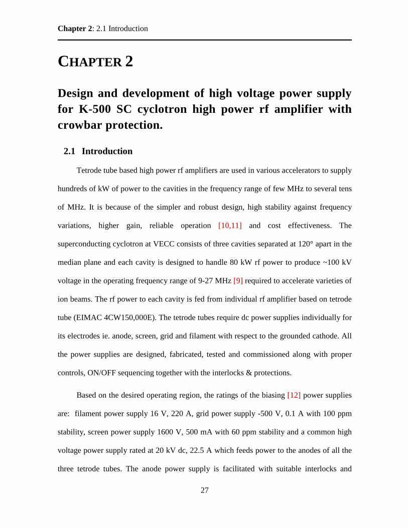
Figure 2-1: Schematic layout of locations of different power supplies and rf amplifiers
used in the K 500 Cyclotron building
High voltage power connection from the anode power supply to the anodes of the
three tubes are done by using three separate high voltage coaxial cable RG220, each ~25 m
cable length through the S-bends. The methodology of high voltage connection for the
coaxial cable RG220 is specially developed in our lab which consists of two sets of copper
blocks, one for the high voltage and other set the shielding connection at some distance
suitable to high voltage level. The control and monitoring of all the power supplies have
been done with local console as well as from remote. In local mode, all the operation to the
power supplies can be done from the local panel kept in power supply room. In remote
mode, parameters control and monitoring is done through Ethernet based Programmer
Logical Controller (PLC) installed in the control room.

Chapter 2: 2.2 Different power supplies for high power RF amplifier
30
2.2 Different power supplies for high power rf amplifier
Different power supplies are discussed in this section required to bias all four
electrodes of three high power tetrode tubes.
2.2.1 Anode power supply
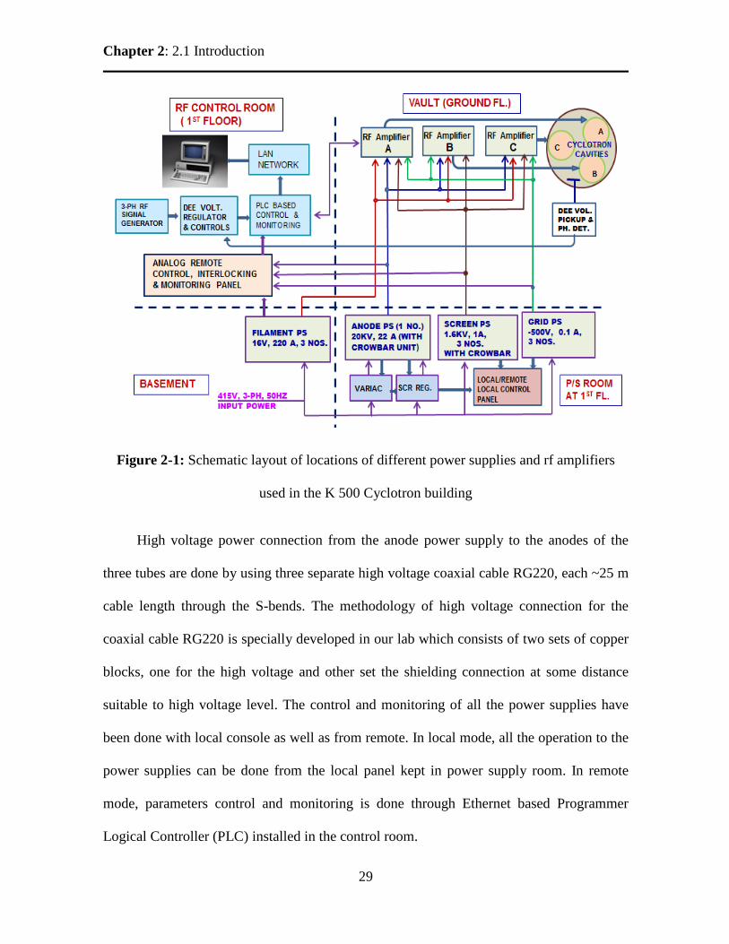
High voltage power supply (HVPS) rated at 20 kV, 22.5 A feeds dc power to the
anodes of all the three tetrode tubes (Eimac 4CW150,000 E). HVPS uses two forced air
cooled main transformers and each transformer has delta connected primary rated at 415 V,
3-phase, 50 Hz, 250 kVA power and two secondary windings, one of which in star and
other in delta, to achieve 30° phase shift for 12 pulse rectification. Each secondary has the
voltage rating of 3700 VL-L, 3-phase, 50 Hz.
Input 3-phase, 415 V supply is connected to two main transformers via air core
chokes (0.1 mH, 400 A) in each line and fast interrupting circuit breakers (CBs) having
tripping time 80 ms (4 cycles). Thus total four secondary windings from two transformers
are connected to their respective 3-phase full wave bridge rectifier assembly giving 5 kV dc
voltage each after rectification [11] and then these are connected in series to provide 20 kV
dc at 600 Hz ripple frequency, as shown in Figure 2-2. The rectifier assembly consists of
12 avalanche diodes (each rated at 1.6 kV, 40 A) connected in series in each limb. The use
of avalanche diode relieves from using series connected R-C network for voltage
equalization. Thus all four rectifier assemblies consist of total 288 diodes mounted on
individual heat sinks. The heat sinks are fixed on glass epoxy sheet inside a cabinet
providing an isolation of ~40 kV and connected to the transformers with high voltage
Teflon insulated cable.
Chapter 2: 2.2 Different power supplies for high power RF amplifier
31
Figure 2-2: Schematic diagram of anode power supply with ignitron and a tube.
A primary SCR controlled soft start feature is incorporated in the primary side of the
first transformer to provide half of the voltage, i.e. 10 kV dc. In the primary side of the
second transformer, oil cooled, 3-phase, high current (400 A) variac is used to adjust the
output voltage on-line between 10 kV to 20 kV dc depending upon the requirements. The
protections and interlocks such as, dc over current, input over current, water flow fail in
ignitron, over temperature at various components, cooling fan fail, phase fail etc. are
implemented along with crowbar protection. Hall type CTs are used for dc over current
protection and dc current monitoring for each tube. Pearson current transformers are used
to sense the internal arc fault condition in each tube and to initiate the crowbar protection
subsequently. Actual photograph of two transformers of anode power supply and Local
control panel is shown in Figure 2-3.

Chapter 2: 2.2 Different power supplies for high power RF amplifier
32
Figure 2-3: Photograph shows the local main control panel with monitoring and fault
indications for all the power supplies and two transformers of anode power supply.
Local control panel has all the arrangements for switching ON-OFF of three set of
power supplies for the Filament, Grid, Screen and an Anode along with individual voltage
and current monitoring and interlocks indications.
The advantages of using two transformers with double secondary windings are as follows:-
a) Facility to adjust output high voltage from 10 kV dc to 20 kV dc.
b) Less voltage stress on HT winding of transformer.
c) The ripple content is greatly reduced to around 1% by utilizing 12 pulse
rectification feature, thus reducing the capacitor filter as well as the stored energy.
d) Less input current harmonic content.
e) Improved input power factor (better than 0.90).

Chapter 2: 2.2 Different power supplies for high power RF amplifier
33
A p-pulse converter under balanced conditions generates a characteristics harmonics
in input side of the order h which [18] is given by h = pn+ 1, where n is any positive
integer. In a 3-phase rectifier system under balanced condition, the expected harmonics are
5th, 7th, 11th, 13th …… which contribute to major part of the distortion in the input.
Total harmonics distortion (THD) will be given by
1
213
211
27
25 ...
VVVVV
THD++++
=
where V1 is voltage amplitude of fundamental frequency. The magnitude of harmonics
currents (Ih) is given by Ih = I1/h, where h is the order of harmonics and I1 is the current of
fundamental frequency.
The vacuum tubes are very much prone to internal arc fault and costly tubes may
become severely damaged if excessive energy is deposited during an internal arc fault.
Crowbar system protects the tubes by diverting the excessive stored energy through
ignitron, a high voltage switch. Thus, crowbar protection system a very critical and
important. During the internal arc fault, the power supply experiences a short circuit
condition until main CB trips. The excessive current flowing through the main transformers
results a huge mechanical and electrical shock [14-17]. So, while designing the
transformer, sufficient factor of mechanical strength of yoke, insulation resistance to
withstand high voltage transients and higher % impedance are considered. The transformer
with higher % impedance offers more resistance which restricts the short circuit current.
Air core chokes in the primary of transformers offer further increase of the impedance
which is advantageous in the event of crowbar. Table 2-1: - Components details and test
results of the anode power supply.

Chapter 2: 2.2 Different power supplies for high power RF amplifier
34
Table 2-1: - Components details and test results of the anode power supply
s. no. parameters values
1 Output voltage + 22.8 kV dc at no load
2 Max output current tested with
amplifier tubes at rf load.
17.5 A (at 18 kV dc)
3 Ripple voltage < 275 V p-p at 18 kV dc.
4 Typical THD in input current 6.7%
5 Input PF 0.95
6 Input Transformer Details
(Each of Two Transformers)
Primary- Delta connected, 415 V, 3-ɸ,
50 Hz, 250 kVA
Secondary windings- star and delta
connected, line voltage 3.7 kV ac.
7 Transformer % Impedance 8%
8 Time of short circuit withstand
test on the transformers
5 s
9 Filter capacitor 30 μF (each 3.75 μF, 40 kV, qty:- 8)
10 Rf filter at output of each
anode
L= 100 µH, C=250 pf in π configuration
The anode power supply circuit simulation is done and required crowbar time is
found to be less than 5 μs considering the load resistance 1000 Ω, as shown in Figure 2-4.
In this circuit, the ignitron and co-axial cable is modeled [18, 19] for simulation so as to
achieve very near to the accurate result.

Chapter 2: 2.2 Different power supplies for high power RF amplifier
35
R71
C6
250pF
V4100Vdc
R810k
R11
1k
R4
0.1
C5
0.1uF
L4
100uH
C7250pF
U2
TCLOSE = 01 2
C3
250pF
X1
2N1595
R14100
C2
250pF
R18
10
R15
1k
C4
100uF
C9
0.1uF
V120000Vdc
L2
10uH
V3
15Vdc
R550k
C1
30uF
L1
0.1H
U19A
LM324
3
2
411
1+
-
V+V-
OUT
0
V2
15Vdc
R3
5
R16100
D1
D1N4009
V+-
+
-
S2
S
VON = 100VVOFF = 400V
R21
3k
R121k
R20
10k
R10
1k
V
L320nH
U20
TCLOSE = 2u
12
R1310k
LOSSYT1
R19
0.6
R2
30
TX2
kbreak
0R1
0.1
C8
370pF
0
R171k
R910k
0
0
Figure 2-4: (a) Schematic diagram of crowbar protection system (b) Simulation result of
the crowbar protection system of anode power supply.
2.2.2 Screen power supply
Three individual power supplies for the screens of three tubes, each rated at 1600 V,
0.5 A, 60 ppm voltage stability have been designed and developed. It uses water cooled
tetrode tube (Eimac 4CW2000) as a regulating device in series, as shown in Figure 2-5.

Chapter 2: 2.2 Different power supplies for high power RF amplifier
36
Figure 2-5: Schematic diagram of screen power supplies for the rf amplifiers.
A 3-phase conventional transformer and rectifier is used and then filtered to get
2500V dc for anodes of three regulating tubes connected as series pass scheme. For each
series tube, individual power supplies are used for the biasing its electrodes. The
electronics circuit for regulation is designed for adjusting the grid of the series tube to
maintain the required output voltage. The screen power supply exhibits reverse current
under certain operating conditions and to avoid it, the output is shunted with a bleeder
resistance of 3 kΩ. In case of a crowbar condition, the power supply fast turns off the
screen and protects the system.
2.2.3 Grid power supply
Grid power supply (rating -500 V, 0.1 A, 100 ppm) is a series regulator type power
supply which uses IGBT as series element for voltage regulation. Grid power supply is a
low ripple and highly regulated power supply with adjustable voltage from zero to -500 V
for biasing the grid. Individual grid power supplies are used for three tubes.

Chapter 2: 2.2 Different power supplies for high power RF amplifier
37
2.2.4 Filament power supply
Filament power supply (rated at 16 V, 220 A) is required to heat up the filament
which does not need very good regulation. It uses a variac in primary of input transformer
for regulation and soft start. It consists of a step down 3- phase transformer, a full wave
bridge rectifier followed by an L-C filter. The part of output voltage is sampled and fed
back to the control circuit which takes care of voltage regulation by controlling the position
of variac. Auto zero of variac and slow ramp up of output voltage is the special feature of
the control card which ramps up in steps by controlling the variac from zero to around 80%
voltage corresponding to output 15.5 V dc in approximately 3 minutes.
2.3 Crowbar protection system
The crowbar protection system is used to protect the vacuum tubes against an internal
arc fault. It detects the fault condition, initiates the corrective action by triggering ignitron
very fast and discharges the excessive energy [20]. An ignitron (Part No:- 7703EHV,
Make: Richardson Electronics, USA) is used as a high voltage switch which meets the
required criteria, i.e. faster response, indefinite hold off high voltage, ability to transfer
large amount of charge, low conduction impedance etc. A peak current of ~1000 A flows
through the ignitron for short duration of 80 ms till the circuit breakers trip the mains
power and results an electron charge transfer less than 1 C per shot [15, 21]. The stored
energy (~6 kJ) in the filter capacitor is required to be bypassed through the ignitron and
considering the source impedance of the power supply, the conduction of ignitron has to be
initiated within 5 μs after the fault. This protection is one of the most critical parts of the
high voltage power supply without which the tube can be damaged.

Chapter 2: 2.3 Crowbar protection system
38
2.3.1 Crowbar circuit block diagram
The key components used in the crowbar protection system are Pearson current
transformer (CT), high voltage fast acting crowbar switch, pulse transformer, non-inductive
resistors, capacitors, fast SCR, MOVs etc. All these components must be fast acting and
suitable for very high frequency applications.
The Pearson current transformer of Model:-110 (Make:- Pearson Electronics Inc,
USA) is used to sense fast rise of the fault current with improved noise immunity and
isolation from high voltage. It possess wide bandwidth of 20 MHz with 3 dB lower cut off
at 1 Hz, sensitivity 0.1 V/A and response time 20ns. The CTs are calibrated at operating dc
current level with 1 MΩ termination. Based on the experiments, the additional delay in
response time is found to be few ns, which is negligible. This indicates that the dc current
level does not drive the magnetic material into saturation and so there is still some flux
swing available to generate a signal from the fault current. Several models of CTs are
available used at different labs for similar applications [15, 16].
The time delay is measured to be ~2.5 μs between the fault signal sensed by the CT
and the pulse transformer output pulse which is reasonably sufficient to trigger the ignitron
within 5 μs. Table 2-2 shows the key specification of crowbar circuit utilized in the present
high power rf system. Hall type current transformers (HCT) are used for output dc current
measurement purpose and for sensing over current conditions.

Chapter 2: 2.3 Crowbar protection system
39
Table 2-2: Crowbar circuit specification
SN Parameters Values
1. Stored energy in filter capacitor 6 kJ
2. Crowbar time between sensing the
arc and the triggering of Ignitron. ~5 μs
3. Limit of energy deposition in the
tube during arcing.
50 J, (accomplished by
Crowbar Protection System)
4. Peak current in output at short
circuit condition 900 A
5. CB tripping time 80 ms (4 cycles)
6. Charge transfer 1 C per shot, through ignitron
before CB trips OFF.
The fast rise of the arc fault current in each of the three tubes is sensed by respective
CTs. One another CT connected in series is to sense total output current. Thus the isolated
signals from four CTs are fed to the crowbar electronics controller card and after
conditioning, the signals are compared with a trip threshold voltage. Then the signals are
fed to a latching circuitry for visual indication and fault diagnostics. The latched signals are
then gated together to generate a mono-shot pulse of duration ~100 ms to trigger a SCR. A
capacitor, charged at 800 V, is rapidly discharged through the SCR connected in series with
a pulse transformer and output fast rise high voltage (~2.8 kV) pulse so generated is used to
trigger the ignitron, as shown in Figure 2-6. Simultaneously, crowbar controller card sends

Chapter 2: 2.3 Crowbar protection system
40
Figure 2-6: Schematic of scheme of crowbar protection system.
a hard wired command to trip the mains power circuit breakers (CBs) and also from the
PLC to trip CBs for redundancy. A manual push button switch is also provided for local
crowbar testing. After the tripping of CBs, the system can be made ON for the next
operation only after a reset from local or PLC.
2.3.2 Timing calculation
During an arc fault, the short circuit current flows through the tube is the sum of
currents from filter capacitors and power supply,
ISC = IPS + IC (2.1)
where ISC is short circuit current in output,
IPS is the current from the power supply transformer, IC is the current from the filter
capacitors.

Chapter 2: 2.3 Crowbar protection system
41
IPS = impedancepercentagecurrentloadFull
x100
= 59
22.
x100 ≅ 230 A (2.2)
where total 9.5% impedance is considered for transformer and input chokes.
IC = filterRC/tmaxc e)R
V( −
= filterRC/tmaxc eI −
≅ 667 x filterRC/te− (2.3)
where maxcV is the maximum voltage and filterRC is the time constant of capacitor
discharging current, R is the equivalent resistance in series with filter capacitor which is
30Ω. Since, the limitation of energy dissipation is 50 J. So, the crowbar timing can be
calculated as:-
JtIVtIV crowbarCoutcrowbarPSout 50≤××+×× (2.4)
)II(Vt
CPSoutcrowbar +×
≤50
))e(I()e(Vt
filtercrowbarfiltercrowbar RC/tC
RC/tmaxc
crowbar2301
50
+−×≤
−− (2.5)
By using the fsolve function of MATLAB for solving for the crowbar timing and found
to be less than 5 µs. The result is counter checked by plotting power ( PSout IV × + Cout IV × )
versus time graph given by Eq. 2.4. The area is calculated by using trapz function of
MATLAB which gives 4.57 µs crowbar time at 50 J energy.

Chapter 2: 2.3 Crowbar protection system
42
2.3.3 Test setup and wire selection
The crowbar system performance is checked by the wire survivability test which
provides a calibrated measure of energy deposition at load end. The wire fuses during the
test, if the energy absorbed by the wire is more than its fusing energy which is fixed for a
uniform cross section of fixed length. A thin copper wire of 33 SWG of a length 150 mm is
chosen whose fusing energy is ~30 J [18] which can safely measure the energy deposition
less than 50 J, the limit of energy deposition in the tube during internal arc condition.
An experimental test setup is made ready by using a high voltage vacuum relay in
series with a small length (~150 mm) of thin copper wire (33 SWG wire) and the setup is
connected across the output terminals of anode power supply. To conduct the crowbar test,
the power supply is energized to the desired level. Then the fault is initiated by closing the
vacuum relay and allowing the short circuit current to flow through the wire. The fault
signal, sensed by a CT, finally triggers the ignitron and at the same time, a trip command is
generated which opens the CBs within 80 ms. If the crowbar system works properly, the
thin wire would survive and then it concludes that energy deposition is less than its fusing
energy. Similar tests are performed repetitively to check the capability of the crowbar
system and its perfect functioning.
The energy of a small length of 33 SWG copper wire is calculated as the function of
volume (or length for different wire gauges) by using the heat energy equation as follows.
Energy = ( V . ρcu ) . ( Ccu .( Tm – Ta ))
The volume of wire, TCEnergyV
cucu ∆=
..ρ (2.6)

Chapter 2: 2.3 Crowbar protection system
43
where, cuρ is the density and cuC is the specific heat of copper and T∆ is the temperature
difference. Melting temperature of copper is Tm = 1083o C, Let, the ambient temperature be
25o C then the value of T∆ is = Tm – 25=1058 o C. cuρ = 8900 Kg/m3, cuC = 385 J/(Kg×K).
Putting all the values in Eq. 2.6, the volume V = 13.88 mm3 is required to fuse at 50 Joule
energy. In our case, the length of wire used is 150 mm whose fusing energy is only 30 J.
Figure 2-7 shows variation of wire length of different wire gauges at a fixed fusing energy.
Figure 2-7: Graph showing the calculated length with respect to wire gauge for a fixed
fusing energy.

Chapter 2: 2.4 Data acquisition
44
2.4 Data acquisition
The control and monitoring of the rf system including the power supplies are done by using
SIEMENS programmable logic controller (PLC) modules. These modules are controlled by
a master CPU (CPU 315-2 DP) consisting of a communication processor CP-343-1. This
CPU communicates with other modules via Ethernet with maximum 32 modules. In order
to monitor/capture the analog parameters of rf system as well as voltages and currents of
power supplies, SM-331 module is used. It is an isolated 8 channel, 14 bit resolution analog
to digital converter (ADC) having the conversion frequency of 10 kHz. The ADC takes 4-
20mA standard current communication for the configuration of different analog signals to
be captured. However 6 mA is the lower limit and 18mA is the upper limit is assigned for
the calibration. SM-332 is used as a 12 bit isolated and 8 channels digital to analog
converter (DAC) which is generally used to provide analog signal from computer to set
different parameters of the rf system. Here also 6 mA to 18 mA range is used to provide the
anode power supply to set the voltage 0 to 20 kV and similarly for other auxiliary
parameters of the rf system. For the control and monitoring of various interlocks, i.e. water
interlock, door interlock, over current, over voltage etc., SM-321 and SM-322 modules are
used as a digital input and output respectively.
The master device (315-2 DP) based on the PROFIBUS is to communicate with the
other slave devices (sensor and actuator). The graphical user interface (GUI) is developed
in VECC in java for monitoring and controlling various parameters of sub-systems with 1s
refreshing rate.

Chapter 2: 2.4 Data acquisition
45
Figure 2-8: RF system control and monitor GUI.
2.4.1 Interlocks and sequence of instruction
The PLC controller checks the sequential operations of related interlocks to make the
power supplies ready for ON in proper sequence. It first checks the start-up interlocks, such
as low conducting water (LCW), door closed, vacuum, cooling system before the filaments

Chapter 2: 2.4 Data acquisition
46
of rf amplifiers are ready for ON. A PLC screen shot is shown in Figure 2-8 where the
parameters monitoring along with the status of interlocks can be visualized. Once all the
start-up interlocks are cleared, the filament power supplies become ready for ON.
Similarly, after filament, sequence is followed as grid, anode and finally screen power
supply. The GUI is made in such a way to follow the above sequence of putting ON the
power supplies. Reversed sequence is followed during shutdown.
2.5 Test results and discussion
The system performance and protective capability of the crowbar system is
demonstrated by using wire survivability test which gives the measured value of the energy
deposition. Initially the card level tests are performed i.e., firing sequence and their
respective delays between the signals are carried out at various points.
Time (1μs/div)
Figure 2-9: Ch-1- A 24 V voltage is applied corresponding to a simulated fault (20 V/div),
Ch-2- Pulse transformer output showing 2.8 kV pulse at rise time 1.5 μs (500 V/div).

Chapter 2: 2.5 Test results and discussion
47
As shown in Figure 2-9, Ch-1 shows a dc voltage of 24 V which is applied at the
fault sensing input to simulate the fault condition and delays. Ch-2 shows the pulse
transformer output voltage 2.8 kV peak with 1.5 μs rise time. The result shows that the
delay in response of pulse transformer is 1 μs after the fault and pulse transformer rise time
is 1.5 μs. Thus total time delay is 2.5 μs between occurrence of a fault and the trigger pulse
to the ignitron.
The wire survivability test with a thin copper wire of 33 SWG of length 150 mm is
performed successfully at ~18 kV voltage level in output.
Figure 2-10: Ch-1(top)- output voltage at 18 kV (10 kV/div), Ch-2 (middle)- current flows
through wire by using a CT (100 A/div), Ch-4 (bottom)- signal for tripping the CBs
simultaneous to the ignitron trigger pulse. X- axis denotes Time scale with 1 μs/div.
The test setup, consisting of high voltage relay in series with thin copper wire, is
connected across the power supply output terminals. Output voltage is set at desired
voltage level. All other protective systems are kept in ready condition before the fault is

Chapter 2: 2.6 Summary and conclusion
48
created by closing the high voltage relay. The wire survivability tests are successfully
conducted.
In Figure 2-10, Ch-1 is the trace of output voltage at 18 kV dc before the fault. Ch-2-
shows the current through the wire shoots up to ~500 A after the fault occurs. The current
will continue to increase till the ignitron turns into full conduction within 5 μs. Ch-3-
shows the pulse generated to switch off the CBs simultaneous to the ignitron trigger pulse.
The ignitron is triggered within 5 μs and thus the thin wire is survived. The crowbar tests
are repeated successfully and that can be enough to conclude the energy deposition at load
end within the permissible limit.
2.6 Summary and conclusion
The design, fabrication, commissioning and testing of total power system for all the
three rf amplifiers tubes have been accomplished within the stipulated time and total rf
systems have been in operation continuously since more than 6 years on round the clock
basis for the tuning and beam extraction from the cyclotron. After the installation of anode
power supply, heat run test was performed with the tube in dc condition. The power system
along with the rf amplifier was tested with water cooled dummy rf load up to 70 kW. The
real time measurement of rf system parameter implies the satisfactory operation of these
power supplies with the tetrode tube based rf amplifiers.
During the testing of Anode power supply, two major challenges were encountered
which were subsequently resolved. All the cabinets are solidly grounded and the
components at high voltage level must withstand at least double the working voltage.
During the insulation voltage withstand test of high voltage rectifier assembly, some

Chapter 2: 2.6 Summary and conclusion
49
problem was noticed. Excessive leakage current and heavy corona discharge was observed
even at lower voltage inside rectifier cabinet which could lead to a voltage breakdown. It
was solved by re-mounting the diodes on glass epoxy channel and FRP angle providing
more isolation and tested up to 40 kV dc. Next, there were some problems due to the noise.
It was also observed that the noise and transients in the output dc voltage was creating
spurious triggering. It was resolved by making a dedicated grounding pit and their
connections with braided copper conductor with larger cross section. There were some
minor problems during crowbar testing. The crowbar circuit design was finally done after
some trials by using faster and better components to minimize the delay and finally the
desired system response time was achieved and then the wire survivability test could be
successfully conducted.
Chapter 3: 3.1 Introduction
50
CHAPTER 3
High voltage power supply (-30 kV, 3.2 A) with crowbar protection for Inductive Output Tube based rf amplifier system
3.1 Introduction
Particle accelerator that produces ion beam of energy greater than 20 MeV generally
requires a high power rf amplifier source which normally made by either by using solid-
state devices or by using vacuum tubes, ie., tetrodes, Inductive output tubes, klystrons,
magnetrons, gyrotrons etc. The IOT based rf amplifier is developed for the use to pursue
research and development activity in superconducting rf cavity project at Variable Energy
Cyclotron Centre (VECC) Kolkata. The state-of-the-art technology of IOT-based high
power rf amplifier is designed, developed, and tested at VECC. A high voltage power
supply rated at negative polarity at 30 kV dc, 3.2 A is required for biasing cathode of IOT
with crowbar protection. As a part of the project, the design and development of high
voltage power supply for IOT rf amplifier has been taken up for testing multi cell
superconducting cavity.
A test stand was planned to be developed for preliminary testing of IOTs and also for
periodic conditioning on regular basis during ideal storage time. IOT has been planned to
use as our maximum operating frequency is of the order of 1.3 GHz. IOT based amplifier is
most suitable for the medium power and for Ultra high frequency (UHF) range i.e. 300
MHz to 3 GHz.
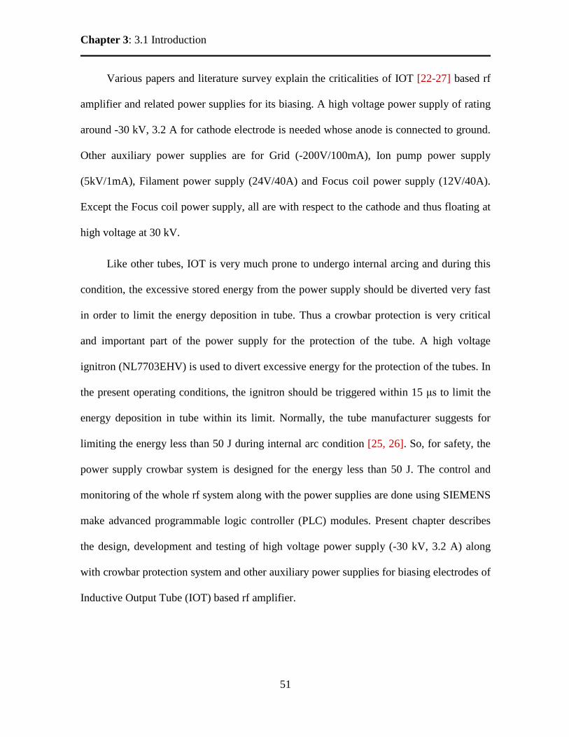
Chapter 3: 3.1 Introduction
51
Various papers and literature survey explain the criticalities of IOT [22-27] based rf
amplifier and related power supplies for its biasing. A high voltage power supply of rating
around -30 kV, 3.2 A for cathode electrode is needed whose anode is connected to ground.
Other auxiliary power supplies are for Grid (-200V/100mA), Ion pump power supply
(5kV/1mA), Filament power supply (24V/40A) and Focus coil power supply (12V/40A).
Except the Focus coil power supply, all are with respect to the cathode and thus floating at
high voltage at 30 kV.
Like other tubes, IOT is very much prone to undergo internal arcing and during this
condition, the excessive stored energy from the power supply should be diverted very fast
in order to limit the energy deposition in tube. Thus a crowbar protection is very critical
and important part of the power supply for the protection of the tube. A high voltage
ignitron (NL7703EHV) is used to divert excessive energy for the protection of the tubes. In
the present operating conditions, the ignitron should be triggered within 15 μs to limit the
energy deposition in tube within its limit. Normally, the tube manufacturer suggests for
limiting the energy less than 50 J during internal arc condition [25, 26]. So, for safety, the
power supply crowbar system is designed for the energy less than 50 J. The control and
monitoring of the whole rf system along with the power supplies are done using SIEMENS
make advanced programmable logic controller (PLC) modules. Present chapter describes
the design, development and testing of high voltage power supply (-30 kV, 3.2 A) along
with crowbar protection system and other auxiliary power supplies for biasing electrodes of
Inductive Output Tube (IOT) based rf amplifier.

Chapter 3: 3.2 Block diagram of IOT based RF amplifier
52
3.2 Block diagram of IOT based rf amplifier
The block diagram and layout of IOT based rf amplifier system along with its
auxiliary power supplies are shown in Figure 3-1. The Thales make IOT TH793-1 is
installed along with all necessary electrical and services connections i.e. low conductivity
water (LCW) lines, ion pump etc. The negative polarity of the high voltage power supply
(HVPS) at -30 kV is connected to the cathode electrode of IOT with respect to the
grounded collector. The electron beam is formed by a gridded, convergent-flow electron
gun and confined by an axial magnetic field. The biasing of the gun is done in such a way
so that no current flows except during the positive half-cycle of the rf input. Thus the
electron bunches are formed which are accelerated through the constant potential
difference between the cathode and anode [22, 23].
Figure 3-1: Scheme of IOT based rf system with all the power supplies and PLC.

Chapter 3: 3.2 Block diagram of IOT based RF amplifier
53
Other auxiliary power supplies such as, filament, grid and ion pump along with I/O
modules for their control are installed on a high voltage deck. The motive of putting them
on the high voltage deck is to provide high voltage isolation as these power supplies
operate with respect to cathode which is floating at high voltage. For monitoring and
controlling these power supplies, PLC based data acquisition systems is installed which
communicates the command signal via fiber optic cable to the PC. The details of individual
systems and their test results are mentioned in following sub-sections.
3.2.1 High voltage deck
A high voltage deck is specially developed for keeping the power supplies, ie.
filament, grid and ion pump which are floating at high voltage at 30 kV. Distributed I/O
control modules are also kept on the deck for their control and monitoring.
Figure 3-2: Photographs of (A) high voltage deck consisting of three power supplies (Ion
pump, Filament and Grid power supply) and isolation transformer at bottom (B) PLC based
control system connected through optical fibre link.

Chapter 3: 3.2 Block diagram of IOT based RF amplifier
54
The deck is fabricated by using glass epoxy and housed inside a grounded metallic
cabinet for safety. The multiple racks have been provided for the power supplies. All the
sharp edges are covered with corona guards. The isolation of high voltage deck is tested up
to 45 kV. The electrical power for the systems at high voltage is provided by a single
phase, resin cast isolation transformer of 4.5 kVA, isolation voltage 45 kV. The photograph
of high voltage deck consisting of all three auxiliary power supplies with isolation
transformer is shown in Figure 3-2(A) and PLC based control system in Figure 3-2(B).
3.3 HV power supply (-30kV, 3.2A)
High voltage power supply (HVPS) is for biasing the cathode of the IOT with respect
to grounded anode. A primary SCR based phase angle controlled topology has been
adopted for the voltage regulation as shown in Figure 3-3. During starting condition, the
firing angle of SCRs slowly increases till the required voltage is achieved and at operating
condition, these primary back to back SCRs offer voltage regulation by varying the firing
angle. HVPS uses two forced air cooled transformers, each having two 3-ph secondary
windings connected in star and delta in order to have 30° phase shift for 12 pulse
rectification feature. Primary of each transformer is delta connected and rated at 415 V, 3-
ph, 50 Hz whereas each secondary rated at 5800 V, 50 Hz. Each secondary connected to a
3-ph bridge rectifier assembly and the rectified dc voltages are then connected in series to
achieve rated output voltage, like our previous HVPS [6].
This feature helps us in getting less ripple voltage at 600 Hz, less harmonic content in
supply current and improved power factor. Input 3-phase, 415 V, 50 Hz is connected to the
transformers via circuit breakers (CBs), air core choke (0.3 mH) and back-to-back SCRs in
each line. In order to produce 30 kV dc, each secondary of the transformers uses 3-phase
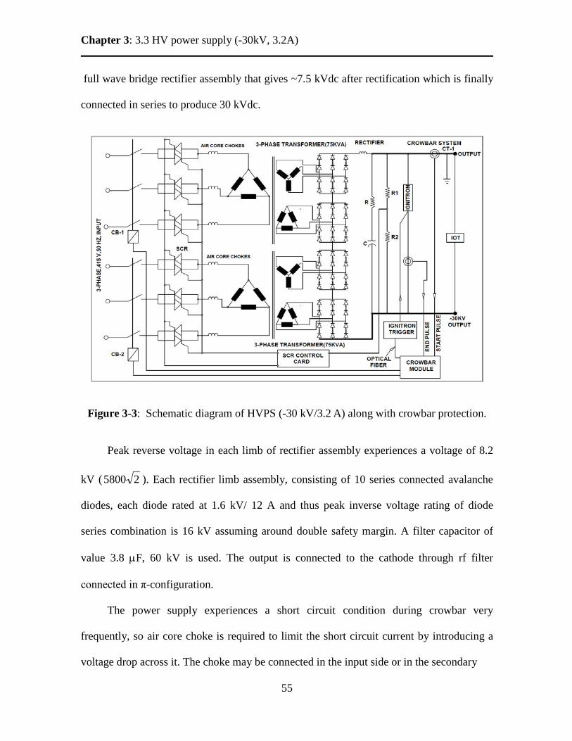
Chapter 3: 3.3 HV power supply (-30kV, 3.2A)
55
full wave bridge rectifier assembly that gives ~7.5 kVdc after rectification which is finally
connected in series to produce 30 kVdc.
Figure 3-3: Schematic diagram of HVPS (-30 kV/3.2 A) along with crowbar protection.
Peak reverse voltage in each limb of rectifier assembly experiences a voltage of 8.2
kV ( 25800 ). Each rectifier limb assembly, consisting of 10 series connected avalanche
diodes, each diode rated at 1.6 kV/ 12 A and thus peak inverse voltage rating of diode
series combination is 16 kV assuming around double safety margin. A filter capacitor of
value 3.8 µF, 60 kV is used. The output is connected to the cathode through rf filter
connected in π-configuration.
The power supply experiences a short circuit condition during crowbar very
frequently, so air core choke is required to limit the short circuit current by introducing a
voltage drop across it. The choke may be connected in the input side or in the secondary

Chapter 3: 3.3 HV power supply (-30kV, 3.2A)
56
Figure 3-4: Simulation schematic for cathode power supply.
Figure 3-5: Simulation result shows (A) improvement of power factor (B) the reduction of
input side current during short circuit condition and in (C) reduction of ripple voltage.
With L1 only at input
With L2 only at dc side
(With L1)
With L1
(With L2)
With L2

Chapter 3: 3.3 HV power supply (-30kV, 3.2A)
57
side after rectifier assembly. The circuit diagram is shown in Figure 3-4 and simulated
with air core choke (L1 = 0.3 mH) connected in input lines and compared with the
equivalent choke (L2 = 2 H) in secondary side as L-C filter. The simulation is performed
using PSIM software for both conditions and simulation results shows improved power
factor in case of chokes at primary side (0.3 mH) rather than equivalent inductor 2H
referred to the secondary side, as shown in Figure 3-5 (A). It is also observed that
introduction of primary side choke reduces the initial short circuit current as well as output
ripple voltage, as shown in Figure 3-5 (B) and Figure 3-5 (C). Finally, air core chokes,
each rated at 0.3 mH, 250 A, are connected in each line of the primary side of the
transformer.
Primary side choke value is optimized in such a way to add more impedance for more
voltage drop across it during short circuit without much affecting the regulation during
normal operation. By this way, short circuit current level will be reduced. So, as a tradeoff
between these two parameters, approx. 50% of line voltage drop (415*0.5 = 207 V) across
it is assumed during short circuit condition. The transformers are rated for primary current
102 A at full load and percentage impedance 8%. So, transformer may experience
maximum primary short circuit current (ISC) = 102x100/8= 1275 A. Thus, theoretical
calculation gives the choke value L1 = Iscf .2.2
207π = 0.28 mH (3.1)
Thus, air core choke of value 0.3 mH is optimized which will create a voltage drop of
~10 Vac across each choke at full load current. This will cause an extra voltage regulation
of maximum 4% which is permissible for our requirements. The input choke when referred

Chapter 3: 3.3 HV power supply (-30kV, 3.2A)
58
to secondary side of transformers and equivalent value of filter choke value is calculated to
be ~2 H. Table 3-1 shows the specification of main cathode power supply.
Table 3-1: Specifications of high voltage power supply for IOT cathode
S.No. Parameters Values
1 Max. output voltage 0 to -30 kV dc
2 Output current 3.5 A,
3 Input voltage 415V AC ± 10% , 3 phase, 50 Hz
4
Mains transformer
details
No. of transformers= 2 Nos.
Each rated at 75 kVA, primary delta at 415 Vac and
2 secondaries in Star & Delta each at 5800 V ac VL-L,
frequency 50 Hz.
Tr. configuration Dy11d0.
Tr. % impedance= 8%.
5 Filter capacitor 3.8 µF, 60 kV
6 Ripple voltage (p-p) <0.5%
7 Load regulation < 0.5% (for 10% load variation)
8 Line regulation < 0.5% (± 10% of input AC variation)
9 Input PF ~ 0.95
10 Shutdown time during
fault condition
< 15 μs crowbar followed by CB trip within 250 ms.
11 Energy limitation < 30 J, Initial stored energy = 1800 J
12 Remote interface
RS-232 / 485 based
communication with PC and
Graphical User Interface (GUI) for operation and
monitoring.
13 Safety interlocks
Input over current, over voltage, dc over current,
phase fail, crowbar protection, ignitron water flow,
over temp of power components, door switch open.
14 Over current setting 110% of rated current.

Chapter 3: 3.4 Other power supplies for IOT
59
3.4 Other power supplies for IOT
Apart from cathode power supply, other auxiliary power supplies are required for the
biasing of the IOT. These are Ion pump power supply rated at 5 kV/1 mA, Grid power
supply rated at -200 V/100 mA, Filament power supply rated at 24 V/40 A and Focus coil
power supply rated at 12 V/40 A. All of the above mentioned power supplies are based on
switching type having features such as, voltage and current regulation and computer
controlled. Except Focus coil power supply, these power supplies are kept at high voltage
deck and input power is fed from an isolation transformer. A PLC based system is kept at
high voltage deck which controls and monitors these power supplies through an optical
fibre link and a GUI is made to control all the power supplies through the PC.
3.5 Supervisory control and monitoring
The supervisory control and monitoring of the IOT based rf amplifier system has
been done remotely in computer via Graphical user interface (GUI) developed in Labview
software. The Labview software bridges the gap between application software to actual
driver signal. These signal finally control and monitor the SIEMENS make PLC modules.
The optical fibre link has been used for transferring control signal from one potential to
other high potential (HV deck) or vice versa. A PLC module (CPU 315-2DP) is used as a
master controller that takes the optical signal coming from remote PC. After processing the
signal, it addresses the PLC which acts as slave device for monitoring and controlling
interlocks, auxiliary power supplies etc. SM-331 module is used to capture analog voltages
that are used for monitoring purposes. It is an isolated 8 channel, 14 bit resolution analog to
digital converter having the conversion frequency of 10 kHz.

Chapter 3: 3.5 Supervisory control and monitoring
60
For controlling the device, module SM-332 is with 12 bit resolution for digital to
analog converter. At a time 12 channels can be controlled using SM-332. The loop time of
the data acquisition system is 10 ms. It would be worth to mention that the whole IOT
based rf system follows the sequence of operation during start up. It first checks interlocks
for start-up, such as low conducting water (LCW), door closed, vacuum, and cooling
system before turn ON of the IOT power supplies starting from Filament.
3.6 Crowbar system for IOT based amplifier
The crowbar protection is very important and crucial system for the protection of high
power amplifier tubes against internal arc fault. A high voltage crowbar switch is
connected across the output tube which is used to bypass the energy during an internal arc.
Figure 3-6: Scheme of crowbar protection system

Chapter 3: 3.6 Crowbar system for IOT based amplifier
61
An energy diverter topology is adopted by using an ignitron (NL7703EHV) to bypass
excessive energy through it very fast within 15 μs time. The crowbar control unit senses the
fault condition and triggers the ignitron very fast and the time delay is a critical factor
which amounts to energy dump. The schematic diagram for crowbar protection system is
shown in Figure 3-6. In this case, to limit the safe amount of energy less than 30J, the
ignitron must be triggered within 15 μs followed by tripping off the CBs. During crowbar,
transformer experiences a short circuit current resulting a huge electrical and mechanical
shock.
With refer to the schematic diagram shown in Figure 3-3, based on the stored energy
in the filter capacitor during normal operation, the ignitron trigger time must be less than
15 μs followed by tripping off the CBs for attaining the safe limit the deposition of [28, 29]
energy across the IOT TH793. The time can be calculated [6] as:
The total current flow during short circuit (Isc) during arcing is represented as:
fcplsc III += (3.2)
Ipl is transformer short circuit current and IfC filter capacitor current. Ipl can be obtained as:
impedancepercentagerTransformecurrentloadfullrTransformeI pl =
= %83.7 ≅ 91A (3.3)
where transformer series impedance is 8% including input chokes. fcI is calculated as:
fcI = filterRCtom ecesis
VcapacitorfilteracrossVoltage /
tanRe)( −
= filterRCtcmeI /−

Chapter 3: 3.6 Crowbar system for IOT based amplifier
62
≅ 115 filterRCte /−A (3.4)
omV is the maximum voltage appear across capacitor during short circuit and omI is the
maximum current. filterRC is the time constant of power supply which is around 1 ms. In
order to limit the energy less than 30 J across IOT, crowbar time cbt can be calculated as:
JtIVtIV cbscoutcbplout 30≤××+×× (3.5)
)91)1(()(30
// +−×≤ −− filtercbfiltercb RCt
fcRCt
omcb eIeV
t (3.6)
From MATLAB optimization toolbox, fsolve function is used to find the value of cbt of
Eq. 3.6 and simulated crowbar timing calculated to be around 18µs. The photograph of the
ignitron and electronic circuitry to sense and trigger crowbar is shown in Figure 3-7. The
heating lamp is placed over ignitron’s anode to keep the anode temperature more than that
of the cathode. This makes fast settling of mercury inside the ignitron and helps the
ignitron to act quickly during an internal arc fault condition in the IOT tube.
As being a negative polarity of HVPS, the anode of ignitron is connected to the
grounded positive terminal and cathode is connected to the negative terminal at -30 kV.
Since, the igniter of ignitron and other parts of the crowbar protection system including
pulse transformer, water cooling system float at high voltage at 30 kV, which is shown in
Figure 3-6. This makes the ignitron assembly a challenging task starting from fixing the
ignitron, maintaining high voltage isolation of more than 30 kV for the crowbar and their
on-line testing. Crowbar system consists of mainly Pearson CT, ignitron NL7703EHV,
pulse transformer, non-inductive resistors, inverter grade high voltage SCR, low ESR

Chapter 3: 3.6 Crowbar system for IOT based amplifier
63
capacitors, MOV etc. The CT (Pearson Electronics Inc, USA, Model:- 110) of response
time 20ns is used to sense the fault current with improved noise immunity at a sensitivity of
0.1 V/A. The fault current is sensed by CT-1 and the fault signal is fed to the crowbar
electronics card.
Figure 3-7: Electronic circuit that senses and trigger crowbar
After conditioning, the signal is compared with a trip threshold voltage by a
comparator and then it latches for interlocking and visual indication. Finally the latched
signal generates a mono-shot pulse (ON time ~1 ms) to trigger a SCR through an optical
fiber for isolation. The SCR rapidly discharges through primary of a pulse transformer to
generate a pulse of 2.5 kV to trigger the ignitron. Simultaneously, crowbar controller card

Chapter 3: 3.6 Crowbar system for IOT based amplifier
64
generates a command to trip the mains circuit breakers (CBs). After every internal arc fault,
CBs are tripped and the system is again made ON after reset from local panel via PLC.
3.6.1 Wire survivability test
Wire survivability test is done to check the crowbar performance at test bench before
connecting to actual crowbar to the tube. In the present case a thin copper wire of 33 SWG
of a length 140 mm is used which has fusing energy < 30 J for testing crowbar of IOT tube.
This test gives the information of energy deposition on load. As the name suggest wire
survivability test is carried out by passing the short circuit current through the wire and if
the deposition is within the safe limit, wire should survive. The test procedure and wire
calculation steps are already described in chapter-2.
3.7 Experimental results and discussion
Photograph of the power supplies and all the arrangements are shown in Figure 3-8
which shows HVPS cabinets along with high voltage deck, IOT assembly, water cooled rf
dummy load etc. Initially, the HVPS and all other auxiliary power supplies were first tested
individually with resistive load. The auxiliary power supplies were then installed at the
high voltage deck along with the control modules and coupled with PLC at ground through
fibre optics. The high voltage power supply for cathode (at -30kV) was tested and also
other parameters were checked with resistive load as mentioned in Table-3-1. The IOT and
water cooled rf load were installed and connected with water line and power supplies. After
ensuring interlocks functioning, the power supplies were put on sequentially and the
systems were tested with the rf load.

Chapter 3: 3.7 Experimental results and discussion
65
Figure 3-8: HVPS in 3 cabinets, cabinet-1 consists of two CBs for transformers, SCRs,
control cards and panels. Cabinet-2 consists of Transformers, six air-core chokes, rectifier
assemblies. Cabinet-3 consists of filter capacitor and crowbar unit consisting of ignitron
assembly, water cooling.
The system was tested up to rf power ~ 42 kW in several steps and all the power supplies
were performed very nicely by keeping the cathode voltage at -30 kV and feeding input rf
signal at 700 MHz to the grid.
In order to check the performance of crowbar system, an experimental setup was
made by using a high voltage vacuum relay in series with a small length (~140 mm) of 33
SWG copper wire, connected across the output of HVPS. A fault was created by closing
the vacuum relay. The performance is demonstrated by using wire survivability test which
gave the measured value of the energy deposition less than 30 J. Initially, crowbar cards

Chapter 3: 3.7 Experimental results and discussion
66
and the propagation signal delay of the components was tested without high voltage. As
shown in Figure 3-9(a), Ch-1 shows the initiation of fault and Ch-2 shows the pulse
transformer output voltage of 2.5 kV peak with 4 μs rise time after a delay of 3 μs. Time
scale is 5 µs/div. Thus total 7 μs delay is recorded between the fault and ignitron trigger
pulse. The trigger signal from pulse transformer is fed to the ignitron through a co-axial
cable. The crowbar test result tested with 33 SWG copper wires at -27 kV output voltage as
shown in Figure 3-9(b). Similar tests were performed repetitively to check the capability of
the crowbar system and its proper functioning.
Figure 3-9 : (a) Ch-1-The moment fault was created (5 V/div), Ch-2- Pulse transformer
output pulse of 2.5 kV having rise time 4 μs (500 V/div). Horizontal axis indicates time
scale 5 μs/div (b) Ch-1- shows the current profile at 200 A/div and ch-2 shows the output
voltage at 15 kV/div by using a potential divider. Horizontal axis Time scale is 5μs/div.
(b) (a)

Chapter 3: 3.8 Summary
67
3.8 Summary
The HVPS and test stand of IOT-based amplifier system is designed, developed and
tested successfully in VECC. Cathode power supply along with crowbar protection system
was tested with the tubes up to the rated current to perform heat run test. The supervisory
control of the IOT based rf system was also checked and ran successfully with one or two
PC hanging problem. The PC hanging problem was then removed by carefully isolating
high potential and low potential grounds and by providing proper shielding to EMI prone
components. The primary concern of the design was to keep lower level of short circuit
current by incorporating the input air core chokes. Observing the simulation results the
optimized value of input core choke is chosen as 0.3 mH in the primary side. Other
important feature that is discussed is the development of crowbar protection system for a
negative polarity HVPS which is comparatively more difficult than positive polarity power
supply. The crowbar circuit worked successfully after several iterations and finally the
crowbar timing can be optimized to be within 15 µs. The initial sparking in the high
voltage deck was removed by mounting suitable corona guards and high voltage resistance
to the floated devices kept at high voltage deck.

Chapter 4: 4.1 Introduction
68
CHAPTER 4
Crowbar less high voltage power supply rated at -40 kV, 5 A based on pulse step modulation (PSM) technique
4.1 Introduction
Several high voltage power supplies developed for different systems of the
cyclotrons at VECC have been discussed in chapters 2 and 3 by using conventional method
to achieve the regulation, ie., SCR based phase angle controller and by using variac. These
power supplies have been running on round the clock basis and overall performances are
very much satisfactory. In such schemes, as usual, the main disadvantages observed which
are huge power loss, lower efficiency, slow response and high stored energy. This would
result into implementation of ignitron based crowbar protection system which is a very
critical system for the protection of amplifier tubes against internal arc faults.
In the present chapter, a new and emerging technique has been utilized to develop a
high voltage power supply rated at -40 kV, 5 A based on pulse step modulation (PSM)
technique [30-33]. Still the commercial availability of PSM based high voltage power
supplies are limited and are very expensive. In future also, there are requirements of several
high voltage power supplies (HVPS) of various ratings for different accelerator
applications. It was then finalised to develop the technology of high voltage power supply
in-house exclusively for the use in accelerator. This initiative would not only reduce the
manufacturing cost considerably but also this will facilitate for the easy and faster

Chapter 4: 4.1 Introduction
69
maintenance during a breakdown condition. Present development is aimed to utilize a
modern technique meeting all the important criterions, i.e. solid state based modular
construction, crowbar-less design, reliable operation, improved voltage regulation, higher
efficiency, fast response and most importantly easy maintenance.
There are very few manufacturers in the world who manufactures high voltage power
converters utilizing PSM based technique. After going through the literatures and articles, a
design scheme for high voltage power supply was worked out and the control strategy was
finalized. Subsequently, a prototype high voltage system of rating 2.5 kV, 3 A based on
PSM was developed which uses a multi secondary transformers with 4 secondary windings
to power four SPMs modules. DSP based controller was used which communicates through
optical fibre links to all the modules. All the parameters of the power supply were tested
successfully and voltage regulation was achieved better than 0.8%.
This follows the design of actual unit of high voltage power supply (HVPS) rated at -
40 kV, 5 A based on PSM topology in similar fashion. HVPS consists of 60 switched
power modules (SPMs) and each module gets input 3- phase power from multi-secondary
transformer’s secondary. Maximum 52 SPMs are required to be switched on and remaining
8 modules are kept in standby which can be automatically put into operation in case of
failure of any of the running SPMs. Solid state SPM uses an IGBT in series as a buck
converter with a typical output voltage of 780 V at a fixed duty cycle at switching
frequency 5 kHz. The operation involves switching-on the required number of SPMs and
the output voltage can be obtained by modulating their pulse widths and phase delay time.
This results into very low ripple voltage at high frequency which ultimately requires very
small filter capacitor resulting into very small stored energy. Hence there is no need to

Chapter 4: 4.1 Introduction
70
implement a special crowbar protection system. Other advantages of using PSM topology
are modular design, low EMI, less harmonics content, high efficiency [34, 35]. The fine
control of output voltage setting and regulation is accomplished by pulse width modulation
(PWM) of 2 SPMs with variable dc voltage. DSP based control system is developed by
using DSP TMS320F28335 in order to ensure the trouble free operation of the power
supply as well as option for future upgrade without much change in hardware. In case of a
failure of any module, automatically controller will switch on a healthy one after disabling
the bad module and thus enabling it to reduce down time.
4.2 HVPS description
In this section, various components of the high voltage power supply is described in
details
4.2.1 Scheme of HVPS of rating -40 kV, 5 A
The IOT cathode needs a regulated dc high voltage power supply with low ripple
and low stored energy. The negative polarity of HVPS based on PSM is used for biasing
the cathode of IOT whose detailed specification is mentioned in Table 4-1. The HVPS
should be well protected against any of the faults as mentioned, including crowbar. Major
components of HVPS are the multi-secondary resin cast multi secondary transformers,
switched power modules (SPMs), circuit-breaker, high voltage switch, DSP based control
system etc., as shown in the schematic diagram in Figure 4-1. The photograph of HVPS is
shown in Figure 4-2, where all the 60 nos. of SPMs and other accessories are housed on

Chapter 4: 4.2 HVPS description
71
glass epoxy structure and two resin cast multi secondary transformers in rear side and
connected to the modules by using high voltage Teflon cables.
Figure 4-1: Schematic diagram of HVPS rated at -40 kV, 5 A.
Figure 4-2: HVPS showing all 60 SPMs and two resin-cast transformers rear side.

Chapter 4: 4.2 HVPS description
72
Table 4-1: Specifications of HVPS based on IOT requirement
SN Parameters Values 1 Input voltage 440 V AC ± 10% , 3 phase, 50 Hz
2 Max. output voltage Up to -40 kV dc
3 Output current 4 A, (max rating 5 A)
4 Ripple voltage (p-p) <0.5%
5 Load regulation < 0.5% (from 10% to 90% of load)
6 Line regulation < 0.5% (± 10% of input AC variation)
7 Input PF ~ 0.90
8 Output voltage rise time < 250 ms (from 0 to Vmax)
9 Shutdown time during fault
condition
< 20 μs
10 Stored energy <30 J
11 Typical overall efficiency Better than 90%
12 Remote interface
RS-232 / 485 based
communication with PC and
Graphical User Interface (GUI) for
operation and monitoring.
13 Output interlocks
Over voltage, over current,
short circuit due to internal arching,
module failure, IGBT over temp.
14 Mains input side interlocks
Under voltage, over voltage, over
current, phase fail.
4.2.2 Multi secondary transformers
HVPS uses two resin-cast multi-secondary transformers, each having 3-phase star
connected 30 secondaries rated at line voltage 580 V, 50 Hz, to power all 60 SPMs which
are kept at glass epoxy structure. The primary of one transformer is star and other is delta

Chapter 4: 4.2 HVPS description
73
connected whereas all the secondary windings are star-connected to obtain 12-pulse
rectification feature to reduce harmonics content in input current and low ripple voltage at
ripple frequency 600 Hz. The transformer’s 30 output secondary coils on each limb are
kept at equal separation from each other. To provide high voltage insulation, these are then
resin casted after vacuum impregnation to avoid any moisture or dirt. The insulation level
of secondary coils with respect to primary coil as well as core is maintained at 80 kV
whereas between two consecutive secondary coils is maintained at 5 kV. The stray
capacitances CSP between primary to secondary windings and CSS between secondary
windings are the key parameters and smaller the values of stray capacitances, better the
results [36, 37]. The photograph of resin cast transformer mounted in a cabinet is shown in
Figure 4-3. For the efficient cooling, two fans are connected on the top of the cabinet.
Figure 4-3: Actual photograph of a multi-secondary transformer, having overall dimension
(1700x650) mm, H= 1600mm.

Chapter 4: 4.2 HVPS description
74
4.2.3 Switched power modules (SPM)
Each SPM consists of a soft start feature by using contactors, 3-ph full wave bridge
rectifier, filter capacitor, free-wheeling diode, IGBT (SKM75GB176D), snubers, varistors,
LEM current sensor and a control board. Each module uses an inductor at output terminal
to stop to enter the surge current. The HVPS contains total 60 SPMs and each is fed power
from multi secondary transformer’s outputs individually at line voltage 580 V, 50 Hz as
shown in Figure 4-4.
Figure 4-4: Schematic diagram of a SPM
Each SPM consists of soft start feature to avoid a starting surge and EMI due to it.
Input 3-ph, 580 VL-L, 50 Hz from each secondary winding of multi secondary transformer
is fed to the input via contactor and then rectified by using a 3-ph bridge rectifier. Then L-
C filter is used to minimise the AC component of voltage and current present in power
supply after rectification. Inductor L2 is used to prevent any spike to enter due to high
inductive reactance to AC, but quite low resistance to dc. Ripple increases with increase in

Chapter 4: 4.2 HVPS description
75
the load in an inductor filter, but decreases in capacitor filter for an increase in the load. So,
the LC filter is used which is independent of load current or load resistance (RL). A
critical/minimum value of inductor (Lc) is required to insure a continuous conduction
mode. This can be estimated using the following well known formula: f
RL Lc π3≥ where,
f is ripple frequency. Now the value of C can be calculated by formula, LC
Ripple 232
ω= .
In present case a ripple of 0.1% is assumed and accordingly C can be calculated.
Each module is switched type regulator connected in buck configuration by using an
IGBT in series and designed for an output of 780 V at 80% duty cycle at switching
frequency 5 kHz. The switching frequency is chosen much higher than the line frequency
to reduce the size and weight of the output filter. However, with the increase in switching
frequency, switching loss and magnetic core loss increases. The switching frequency of
each module is kept at 5 kHz which is an optimum value for an IGBT. Ultimately the ripple
frequency at output will become N times 5 kHz, where N is nos. of modules, which is
sufficiently high and thus filter requirement is very small.
The output voltage is 780 V when IGBT Q1 is turned-on and zero voltage when
IGBT Q1 is turned-off and during off time, the freewheeling diode bypasses the module by
providing a bypass current path for others. In case of crowbar or any fault condition, the
series IGBT Q1 is turned off and IGBT Q2 is turned on for faster discharge. The control
electronics is designed to interface for communication with the main controller through
optical fibers and allows the switching of IGBTs from local or remote mode. The series
connection of all 60 modules leads to a relatively high complexity of high voltage cable

Chapter 4: 4.2 HVPS description
76
and optical fiber connections. Two SPMs are made vernier modules utilizing PWM type
switching voltage regulator for fine regulation. These SPM’s output voltage varies typically
from zero to 780V depending upon the duty cycle. The control system is developed as per
the algorithm and accordingly a GUI is developed for smooth operation and parameters
monitoring on remote PC. During the operation, due to the proper modulation strategy, the
output ripple frequency seen by the load equals to switching frequency multiplied by
number of modules. This feature allows the higher output ripple frequency at lower
switching frequency. The control cards of SPM takes care of an effective protection in case
of any internal faults and keep the status of health of modules informed to the main
controller through optical fiber communication.
4.3 Control scheme of PSM based HVPS
In this section the detailed control architecture of PSM based HVPS will be discussed
apart from the mathematical calculations, the main flow diagram that will ensure closed
loop feedback by using a controller by using DSP TMS320F28335 and then the
supervisory control will be discussed.
4.3.1 Working principle of PSM
There are N number of SPM modules, each consists of a dc source Vs, a solid-state
switch Si and a freewheeling diode Di, where I denote the number of SPM modules from 1
to N, as shown in Figure 4-5. The total output voltage across load is the sum of the
respective output voltages of each SPM. The output voltage equals Vs for a closed switch S
and zero for an opened switch S for any SPM. In coarse step modulation (CSM) control,
the controller switched on nSPMs (where n <N) in order to get output voltage nVs. The

Chapter 4: 4.3 Control scheme of PSM based HVPS
77
problem arising with this approach is that we can get only integer value of Vs at the output.
But sometime fine steps are to be added and for this, we have added two SPMs for fine-
tuning. The difference between required output voltage and CSM voltage is added with
PWM-pulses, which are generated just by switching on additional steps.
Figure 4-5: Working principle of PSM based HVPS.
Simulation results of four SPMs operated in PSM approach is shown in
Figure 4-6. Each module has equal duty cycle with a fixed phase shift to ensure equal
loading. It can be seen that the output voltage reaches 4Vs with peak to peak ripple voltage
equal to one SPM voltage (Vs) at a ripple frequency four times SPM switching frequency.
Thus it would require 16 times less filter capacitor value that could inherently reduce the
stored energy and therefore easing the need of additional crowbar protection system. At full
voltage, the number of modules will be further increased resulting very low stored energy.
Hence, HVPS utilizing PSM technique does not require an additional crowbar system and
thus it is called crowbar less power supply.
Chapter 4: 4.3 Control scheme of PSM based HVPS
78
Assuming total output voltage Vo, delay time Td consecutive SPM the efficient
frequency fo and modified duty cycle Do can be calculated as follows.
NTTd =
(4.1)
TT
NVV onso = (4.2)
so Nff = (4.3)
( ) sdono NfmTTD −= (4.4)
where fs is the switching frequency of one SPM and N is the number of working
SPM. Vs, Ton, T, Td and fs are input voltage, switch on time, time period, delay time and
switching frequency respectively. N is the total number of switch-on SPM and m is the
integer part of Ton/Td. So the output voltage and efficient frequency can be adjusted by
changing Vs, Ton and fs [38-42].
Figure 4-6: Output voltage waveform with shifted PWM for 4 SPMs

Chapter 4: 4.3 Control scheme of PSM based HVPS
79
As shown in Figure 4-6, the output voltage with 4 SPMs at switching frequency fs =
5 kHz, Vs=780 V at duty cycle of 80%. As control signal of the PSM is based on stage
rotation, therefore the second switch will turn-on T/4 time later than the first one, the third
will turn on T/4 later than second one and forth is turned on T/4 later on than third one and
so on. The output waveform (Vout) shows that ripple voltage (peak to peak) is equal to one
module voltage Vs and ripple frequency equals to four times fs. From Eq. 4.4, the duty cycle
at the output stage is 20%.
Thus the output waveform resulting from PSM modulation gives more advantages.
For N=3, keeping other parameter constant Td =T/3, ripple voltage at output stage is equal
to one module voltage, duty cycle at output stage Do=28%. Similarly, for N=8 Duty cycle
Do=40% and Td =T/8. Thus, Duty cycle of output stage depends on m i.e., integer part of
Ton/Td. If Ton is integer multiple of , Do=0 output is absolutely ripple free. For N=4, Td=
50µs, there are four possible (50µs, 100µs, 150µs, 200µs) for which Do=0 so, the filter
capacitor requirement is almost nil. Hence, in case of four modules there are four duty
cycle points where output is ripple free. Similarly, in N number of power modules there are
N duty cycle points where output contain almost no ripple voltage [43, 44]. This strategy
avoids or minimizes the output filter capacitance requirement resulting very low stored
energy.
4.3.2 Closed loop control program
HVPS consists of total 60 SPMs out of which 58 SPMs having fixed duty cycle and 2
SPMs having variable duty cycle incorporating PWM at switching frequency at 5 kHz for
output voltage regulation. During the load disturbances, the difference between required

Chapter 4: 4.3 Control scheme of PSM based HVPS
80
output voltage and Coarse Step Modulation voltage is added with PWM-pulses and gives
the output voltage within 200 V of set voltage. In order to realize the precise timing control
of the PSM modules, Texas Instrument floating point Digital Signal Processor
TMS320F28335, as shown in Figure 4-7, is used as the core controller to generate pulses
for switch-on and switch-off IGBT for each module. DSP communicates with each SPM
through optical fibre as all the SPMs are floating at high voltage.
The DSP has special purpose CPU that provides ultrafast instruction sequences such
as shift and add, multiply and add which is commonly used in math operation. Also, it has
inbuilt circuit made up of PWM, Analog-to-Digital Converter (ADC) and Input-Output
(I/O) peripherals. These circuit peripherals are mainly used as a controller for the power
electronic converters. The DSP controller is used because of its advantages, i.e., low cost,
embedded floating-point unit, high clock speed, high resolution, on-chip ADCs, high
performance PWM unit. Code composer studio (CCStudio) IDE v3.3 software is used for
the programming of TMS320F28335 [45]. It is the integrated development environment
(IDE) for TI's DSPs. It includes compilers, source code editor, project build environment,
debugger, profiler, simulators and many other features.
Figure 4-7 : TMS320F28335 with PWM output and Analog input

Chapter 4: 4.3 Control scheme of PSM based HVPS
81
Figure 4-8: Block diagram of DSP based HVPS control architecture
ADC input channels are used to receive the feedback of voltage and current signals.
Four to sixteen lines multiplexer (74HC154) is used to turn ON/OFF 16 SPMs and is
controlled using digital input output pins of DSP which is shown in Figure 4-8. Two SPM
modules are controlled using PWM pins of DSP which has been implemented for fine
tuning of the output voltage and also for the regulation and controls. For rest of SPMs,
digital output is used to control switch-on and switch-off according to the required set
voltage. The controller can turn off all the SPMs quickly in case of any faults occurs such
as dc over current or crowbar. Individual SPM is protected against internal faults, i.e. IGBT
short circuit, over temperature and over current. The power supply can be either operated
remotely using graphical user interface (GUI) or from local panel.

Chapter 4: 4.3 Control scheme of PSM based HVPS
82
Figure 4-9: Flow diagram of control architecture
The DSP is used as an independent master controller without slave controllers which
is a simpler design. The DSP based controller has many advantages like flexibility,
accurate, not much affected by the noise, reconfigurable without much change in hardware
etc. The only drawback is slow speed which requires few more ms time to achieve the
desired set value, which in our case is not the serious issue.

Chapter 4: 4.3 Control scheme of PSM based HVPS
83
The control architecture is based on the flow diagram which is shown in Figure 4-9.
Flow diagram starts checking all the interlocks and then it checks the set voltage Vset. Since
the duty cycle is fixed at 80% to 100% and for a specific number of modules, phase shift
(Td) can be calculated. The number of SPMs to turn on is given by n= Vset/780. The fraction
part of Vset/780 V is controlled by two vernier SPMs for regulation.
4.3.3 Supervisory control and monitoring
The supervisory control and monitoring system for all the power supplies including
HVPS is developed in-house by using PLCs and is programmed using Simatic manager
software provided by Siemens. Siemens S7-300 PLC is used which handles all the fields
I/Os. It takes care of all safety interlocks like over voltage, over current, water flow, air
flow etc. along with the start-up interlocks. Auxiliary power supplies, at high voltage deck,
Figure 4-10: HVPS control and monitor GUI.
are controlled by Siemens distributed I/O modules (ET-200) with Ethernet. An Ethernet to
optical and optical to Ethernet channel is used to navigate the control signals from high
voltage deck to PLC. A GUI as a control panel is developed to control the HVPS from PC,
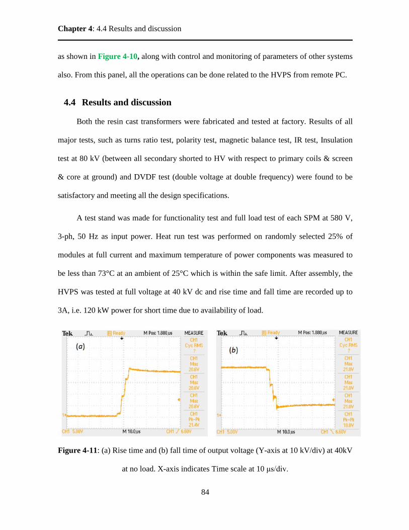
Chapter 4: 4.4 Results and discussion
84
as shown in Figure 4-10, along with control and monitoring of parameters of other systems
also. From this panel, all the operations can be done related to the HVPS from remote PC.
4.4 Results and discussion
Both the resin cast transformers were fabricated and tested at factory. Results of all
major tests, such as turns ratio test, polarity test, magnetic balance test, IR test, Insulation
test at 80 kV (between all secondary shorted to HV with respect to primary coils & screen
& core at ground) and DVDF test (double voltage at double frequency) were found to be
satisfactory and meeting all the design specifications.
A test stand was made for functionality test and full load test of each SPM at 580 V,
3-ph, 50 Hz as input power. Heat run test was performed on randomly selected 25% of
modules at full current and maximum temperature of power components was measured to
be less than 73°C at an ambient of 25°C which is within the safe limit. After assembly, the
HVPS was tested at full voltage at 40 kV dc and rise time and fall time are recorded up to
3A, i.e. 120 kW power for short time due to availability of load.
Figure 4-11: (a) Rise time and (b) fall time of output voltage (Y-axis at 10 kV/div) at 40kV
at no load. X-axis indicates Time scale at 10 μs/div.

Chapter 4: 4.4 Results and discussion
85
The rise time and fall time of HVPS were recorded and shown in Figure 4-11 which
is around 15 μs at no load. The available resistive load of 40 kW was used to test the power
supply at higher current for short time. The line as well as load regulation of HVPS was
tested at resistive load and found to be better than 0.5%. The over current protection at
different current level adjustable from 3.0 A to 6.0 A was performed successfully at lower
voltage.
The power supply as well as rf amplifier tube must be protected against crowbar or
short-circuit caused due to internal arcing. To demonstrate low energy dump (<30 J) to the
load during a fault, wire burn test was performed. For this purpose, a crowbar test set-up
was connected across the output terminals. The test setup consists of a high voltage relay in
series with a piece of a thin 33 SWG copper wire of 140 mm long suitable for 30 J of
energy transfer. The result of crowbar test of HVPS performed at -25 kV is shown in
Figure 4-12. The short circuit current was measured using a LEM CT and a current probe.
Figure 4-12: Short circuit test (CH3: voltage 15 kV/div which is scaled down to 3:1 by
using voltage divider; CH1: current, 20 A/div)
Trigger

Chapter 4: 4.5 Summary and conclusion
86
To perform the crowbar test, a fault condition was generated by closing a high
voltage relay in series with a piece of 33 SWG thin copper wire which is connected across
the output terminals. Once the fault is sensed by a Person CT, the signal is fed to the
controller which is fast enough to send the switch-off command to all the IGBTs in all
SPMs. In Figure 4-12, It can be seen that within 15 μs, the power supply gets complete off
without burning the thin copper wire. The tests were repeated and similar results were
found. The HVPS efficiency is calculated to be better than 96.5% which is very good.
Transformer Loss = 2750 W , Losses in each module = 42 W @ 5 A
Total loss in 50 modules = 42x50 = 2100 W, maximum 50 modules gives required voltage.
Losses in other components = 1550 W, Total Losses = 2750 + 2100 + 1550 = 6400 W,
Thus, Efficiency = 200/(200+6.4) = 96.5 %.
4.5 Summary and conclusion
The HVPS has been developed, installed and tested with available resistive load up
to 120 kW power level for a short time. Due to unavailability of services of IOT, the actual
load installation will take some more time. Individually, all the modules are tested at full
load and found to be compliant and meeting all the specifications. The HVPS is found to
deliver excellent operating performances with inherent redundancy, faster dynamic
response better than 15 μs, low stored energy which is less than 50 J and improved
efficiency which is calculated to be 96.5%. Overall HVPS testing was carried out up to 40
kV at 3 A current (not exceeding 120 kW) for a short time and full current at -25 kV. This
is due to the available resistive load. After the IOT installation and commissioning along
with water cooling and other services, the rf testing will be done.

Chapter 5: 5.1 Introduction
87
CHAPTER 5
Study on harmonics and EMI
5.1 Introduction
The high voltage power supply (HVPS) based on pulse step modulation (PSM)
technology (described in Chapter-4) has been widely used for various applications, ie., rf
amplifiers, Electron Cyclotron Resonance Heating (ECRH) systems etc. The HVPS is a
complex system which contains multi-secondary transformers followed by numbers of
rectification units and switching converters modules. In such situation, there is huge scope
of harmonics generation in the power system mainly due to non-linear behaviour of active
and passive devices. In order to reduce the effects of harmonics, several corrective steps
have been implemented. Heavy magnetic inrush current of the transformer and capacitor
charging may trigger the overcurrent for the mains breaker.
Figure 5-1: A typical soft charging at 440V (CH1- dc link voltage (yellow) from 0V to 620
Vdc, CH2- Input AC current (green) envelop which shows soft start condition of a
transformer showing the soft charging of capacitor filter in time interval of 6s.
X-axis:- Time 1s/div
Y-axis:- Ch-1 Voltage (yellow) 0 to 620 V dc.
Ch-2- AC Current (Green) -40 A to +40 A.

Chapter 5: 5.1 Introduction
88
Sudden inflow of huge inrush current during start causes huge EMI and can disturb
the surrounding equipment. For the protection of breaker and capacitors from overcurrent
as well as the disturbances to other equipment resulting from EMI, a soft start procedure is
necessary [46]. A typical soft start procedure of a module is shown in Figure 5-1 which
describes the flow of magnetising current as well as capacitor charging current slowly at
the time of start. This helps to reduce EMI to great extent. PSM power supply starts up in
two steps: soft start of transformer as well as each switched power modules. Considering
the transient behaviour of soft start procedure, the resistors should be suitably selected
which should balance the current decay time without any oscillation. Optimum resistor
value (R) in series is calculated considering the equation
R2C2 – 4 LC > 0,
So, R > CL2 , where L and C is circuit inductance and capacitance.
5.2 Study on Harmonics and their analysis
Each switched power module (SPM) consists of a 3-ph bridge rectifier followed by
IGBT based buck converter. In a 6 pulse rectifier configuration, [47] the input current
waveform will contain some harmonics and due to that the input current waveform looks as
shown in Figure 5-2. The input current contains harmonics: h = kq ±1, where h is the
harmonic number (integer multiple of the fundamental), k is any positive integer and q is
the pulse number of the converter. This means that a 6-pulse (or 3-phase bridge
configuration) rectifier will exhibit harmonics at the 5th, 7th, 11th, 13th, 17th, 19th, 23rd,
25th etc. multiples of the fundamental. As a thumb rule, the magnitudes of the harmonic

Chapter 5: 5.2 Study on harmonics and their analysis
89
currents is the fundamental current divided by the harmonic number (e.g. the magnitude of
the 5th harmonic would be about 1/5th of the fundamental current). A 12-pulse (or 6-phase
rectifier) will, in theory, produce harmonic currents at the 11th, 13th, 23rd, 25th, etc.
multiples. In reality, a small amount of the 5th, 7th, 17th and 19th harmonics will also be
present with a 12-pulse system (typically the magnitudes will be on the order of about 10%
of those for a 6-pulse drive) [47].
Figure 5-2: Input line current distorted waveform which contains harmonics.
Zero sequence harmonics ( 3rd, 6th, 9th, ….. (6n-3) th ) do not produce a rotating
field [48]. These harmonics circulate between the phase and neutral or ground. The third
order or zero sequence harmonics, unlike positive and negative sequence harmonic
currents, do not cancel but add up arithmetically at the neutral bus. Another set of special
harmonics called “triplens” (multiple of three) which have a zero rotational
sequence. Triplens are the odd multiples of the third harmonic (3, 9, 15, 21……). These
harmonics flow in grounded star connected system and circulate in delta-connected
windings which produce overheating. Positive sequence and Zero sequence harmonics are
responsible for overheating of conductors, whereas Negative sequence harmonics, on the
other hand, circulate between the phases creating additional problems as it rotates in
opposite phasor rotation and produces more core loss [49].

Chapter 5: 5.2 Study on harmonics and their analysis
90
We know that non-sinusoidal periodic complex waveforms are thus generated by
adding together sinusoidal harmonics waveforms at the frequencies multiple of
fundamental frequency which is shown in Figure 5-3 or vice versa. Harmonics are shown
as multiples of the fundamental frequency ( f ), such as: 2ƒ, 3ƒ, 4ƒ, etc. Harmonics is
generalised term used to describe the distortion in a sinusoidal fundamental waveform [47].
A complex and distorted periodic waveform can be split up mathematically into its
individual components of harmonics by using Fourier Analysis Method.
Figure 5-3: Complex waveform formed by adding the waveforms of several frequencies.
The amount of waveform distortion of a complex waveform and its distinctive shape
is directly related to the frequencies and magnitudes of the most dominant harmonic
components. The most dominant harmonic components are the low order harmonics from
2nd to the 19th with the triplens being the worst. The equation given for the value of a
complex waveform will be:

Chapter 5: 5.2 Study on harmonics and their analysis
91
ET = E1 + E2 + E3 +………+ E(n)
ET = V1max sin(ωt) + V2max sin(2ωt) + V3maxsin(3ωt) +…….+ Vnmaxsin(nωt)
Harmonic sequence refers to the phasor rotation of the harmonic voltages and
currents with respect to the fundamental waveform. Normally, the amplitudes of harmonics
is the ratio of fundamental amplitude divided by the harmonics number. If fundamental
amplitude is A, 2nd harmonics amplitude = A/2, 3rd harmonics amplitude = A/3 and so on.
5.2.1 Fourier series
For a periodic function f(x) that is integrable on [−π, π], the number, the function
can be represented as a sum as follows
∑=
≥++=N
nnnN NnxbnxaaxfS
1
0 0)],sin(.)cos(.[2
)(
Where a0 , an and bn are called the Fourier coefficients of function f(x) which can be
expressed as
0,)(10 ≥= ∫
+
−
ndxxfaπ
ππ
0,)cos()(1≥= ∫
+
−
ndxnxxfan
π
ππ
0,)sin()(1≥= ∫
+
−
ndxnxxfbn
π
ππ
The partial sums for f are Trigonometric Polynomials. Since, the functions SN f(x)
approximate the function f(x), and that the approximation improves as N → ∞ Infinite
Series. SN f(x) = ( ) ( )nxbnxaa
nn
n sincos2 1
0 ++∑∞
=

Chapter 5: 5.2 Study on harmonics and their analysis
92
is called the Fourier series of f(x). These trigonometric functions can themselves be
expanded, using multiple angle formulae.
The most commonly-used measure for harmonics is total harmonic distortion
(THD), also known as distortion factor. It is applied to both voltage and current. THD is
defined as the rms value of the harmonics above fundamental, divided by the rms value of
the fundamental. THD of a voltage or current can be defined as
1
24
23
22 ..........
VVVV
THDF
+++=
where Vn is the RMS voltage of n th harmonic and n = 1 is the fundamental frequency.
5.2.2 Harmonics reduction by transformer configuration
The PSM based high voltage power supply (-40kV, 5A) consists of two multi
secondary transformers. First one transformer, primary is Y connected and secondary
windings are Y connected and in second transformer, primary in Δ and secondary windings
are in Y connected. Thus all secondaries are star connected which served in parallel
connection to give output 12 pulse rectification, as shown in Figure 5-4. Line-to-line
transformer voltage ratios are identical for all secondary windings. The top transformer is
in Y-Y connection thus having no phase shift. The transformer in bottom has Δ-Y, thus
having 30° phase shift. Finally, the secondary currents of both the transformers operate in
parallel provide 12 pulse rectification and thus the THD is reduced considerably around
1.25%. Hence, 12 pulse rectification automatically reduces the filter size.

Chapter 5: 5.2 Study on harmonics and their analysis
93
Figure 5-4: Primary transformer connection and analysis of transformers
Assuming the balanced load, each 3-phase secondary undergo 6 pulse rectifications
as shown in Fig-2. From Fourier transformation, it can be seen that being a half wave
symmetry, even-ordered harmonics will remain absent [47, 50, 51]. So, resultant current
can be written as Inet(t) = 2I1 sin(ωt) + 112 1I
sin(11ωt) + 132 1I
sin(13ωt) +………….
Recognizing the pattern shows that the remaining harmonics are h = 12n ±1 , whereas
n=1,2,3…. which leads to the classification “twelve-pulse converter” and this way
harmonics content in input current is reduced to almost half of 6-pulse converter and hence
THD can be improved by using 2 transformers in 12 pulse converter mode. The presence of
harmonics may affect the systems in following way-
a) Skin effect due to higher frequencies and also results more loss.
b) Triplen harmonics circulating in neutral conductor making excessive heating.
c) Negative sequence produces opposite rotating field which reduces flux linkage.

Chapter 5: 5.2 Study on harmonics and their analysis
94
5.2.3 Harmonics standards
For harmonics generation, the system design must have compliance. One of the
major standards is International Electro technical Commission (IEC) European Standards
where EN 61000-3-2 Harmonic Emissions standard is applied to household appliances.
There are four classes Class-A, B, C and D for various purposes. Additional harmonic
current testing, measurement techniques and instrumentation guidelines for these standards
are covered in IEC 1000-4-7 [48].
5.3 Study on EMI and EMC
Electromagnetic interference (EMI) is an unwanted electromagnetic disturbance that
interrupts, obstructs or otherwise degrades the equipment performances which is a major
concern for all the electrical and electronics systems. The sources of EMI have been
commonly identified as the equipment or system incorporating very high rate of switching
voltage or current (dv/dt and di/dt) interacting with parasitic components. EMI produces
two types of emissions; conducted (voltages or currents) and radiated (electric or magnetic
fields in range of few MHz or more). Typically Switch-Mode Power Supplies produce
conducted interference signal (operating in the range of 10 kHz to 100 kHz). For EMI to
exist there must have an electrical noise (EMI) source, a coupling path, and a victim
receptor. Four different types of elementary EMI coupling can be identified: Impedance
coupling, Inductive coupling, capacitive coupling and radiative coupling [52, 53]. The
dominant disturbing phenomena are due to the inductive coupling, followed by capacitive
and impedance coupling, which are relatively more prominent with the increase in
frequency. At much higher frequencies, generally the field strength of radiative coupling
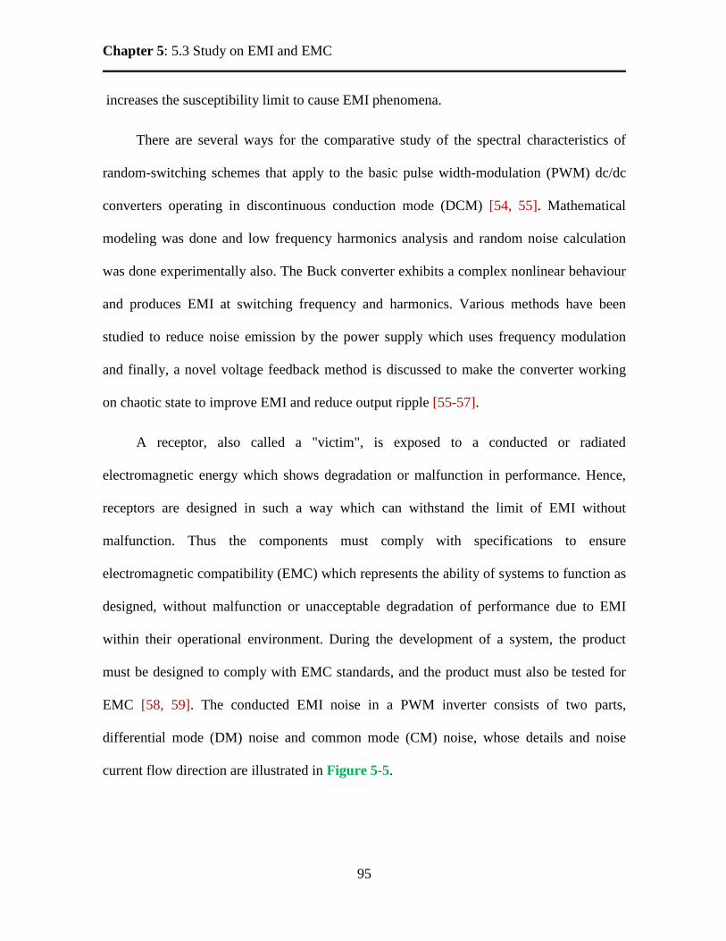
Chapter 5: 5.3 Study on EMI and EMC
95
increases the susceptibility limit to cause EMI phenomena.
There are several ways for the comparative study of the spectral characteristics of
random-switching schemes that apply to the basic pulse width-modulation (PWM) dc/dc
converters operating in discontinuous conduction mode (DCM) [54, 55]. Mathematical
modeling was done and low frequency harmonics analysis and random noise calculation
was done experimentally also. The Buck converter exhibits a complex nonlinear behaviour
and produces EMI at switching frequency and harmonics. Various methods have been
studied to reduce noise emission by the power supply which uses frequency modulation
and finally, a novel voltage feedback method is discussed to make the converter working
on chaotic state to improve EMI and reduce output ripple [55-57].
A receptor, also called a "victim", is exposed to a conducted or radiated
electromagnetic energy which shows degradation or malfunction in performance. Hence,
receptors are designed in such a way which can withstand the limit of EMI without
malfunction. Thus the components must comply with specifications to ensure
electromagnetic compatibility (EMC) which represents the ability of systems to function as
designed, without malfunction or unacceptable degradation of performance due to EMI
within their operational environment. During the development of a system, the product
must be designed to comply with EMC standards, and the product must also be tested for
EMC [58, 59]. The conducted EMI noise in a PWM inverter consists of two parts,
differential mode (DM) noise and common mode (CM) noise, whose details and noise
current flow direction are illustrated in Figure 5-5.

Chapter 5: 5.3 Study on EMI and EMC
96
Figure 5-5: Common Mode (CM) and Differential Mode (DM) current
The common mode (CM) noise is generated mainly due to the high rate of change of
voltage (dv/dt) caused by the switch turn on/turn off, coupled through the parasitic
capacitance between the IGBT collector and the module base-plate heat sink that is
normally grounded. The CM noise current flows through both the input lines into the
ground through the stray capacitance. The differential-mode (DM) noise current (IDM) is
largely due to di/dt in the dc bus as the normal switching operation of the converter and
flows between the phase and neutral lines.
In order to mitigate the effect of EMI, there are various schemes ie., use of EMI
filter, short & twisted cable pair of smaller length which reduces parasitic inductor and
capacitors, snuber circuit etc [59]. Sharp rising edge and falling edges will have more dv/dt
and causes CM noise. Snuber capacitor is used to limit the IGBT turn-off dv/dt. As the
EMI generation is unpredictable [53, 60] and so it needs perfect design, modelling,
simulation and noise spectrum estimation. The most common method is Fast Fourier
Transform (FFT) to get a wide-band varying EMI-spectrum and information of power
spectral density verses problematic harmonic frequencies.

Chapter 5: 5.3 Study on EMI and EMC
97
5.3.1 EMI characterisation
The continuously growing market demands for fast-switching power supplies and
giving rise to the need of more controlled methodologies to meet regulatory
electromagnetic compliance (EMC) requirements [60-62]. The resonant converters type
switching mode power supplies (SMPS) are in use implementing zero-current (ZCS) or
zero-voltage (ZVS) operation which minimizes switching losses and noise. Also, the
conducted and radiated noises emitted from SMPS making the need of proper input filter
design which is also an intricate part of the overall power supply design. EMI can be in the
form of conduction or radiation [63]. Conducted EMI passes through supply lines and
interconnecting wires and is divided into Common Mode (CM) and Differential Mode
(DM). Differential mode follows the same path as the input power while the common mode
has a current path through earth (chassis). Common-mode (CM) emissions are generally
due to the rapid switching of voltage across parasitic capacitances [64].
General topology of the input filter section of power supply for suppression of EMI
noise is as shown in Figure 5-6. In the diagram, Cy elements represent Y-Capacitor values
Figure 5-6: EMI filter between switched power module and mains supply

Chapter 5: 5.3 Study on EMI and EMC
98
which is chosen to effectively shunt common mode currents from reaching the power
supply. Capacitor Cx elements are X-Capacitors used to control differential mode
harmonics [65, 66]
Inductor L1 is used with a purpose of further suppressing high frequency CM noise
currents while inductors L2 limits deferential modes by utilizing the leakage capacitance
resulting from the proximity of windings from one another. The filter also serves the
essential purpose of preventing noise fluctuations from AC input signal to the power
supply. When designing to meet regulatory emission standards, proper attenuation of the
noise requires an adequate number of filter stages. There may have Single-section or
multiple sections of EMI filters with careful attention to the parasitic. While choosing a
capacitor, the effect of ESR and ESL is very important which affect the resonant frequency.
Electromagnetic interference (EMI) filters have been used for power electronics converters
to attenuate switching noise to meet the EMI standards. However, because of the parasitic
in the filters, it cannot attenuate high-frequency noises efficiently. There are few techniques
to mitigate the effects [58, 67-69].
There is no setup available at present in our lab for the measurement of conducted
EMI, but some labs have this facility for the measurement of noise. Line Impedance
Stabilization network (LISN) is one of the most common part whose schematic is shown in
Figure 5-8 to measure the conducted noise emission which propagates from the device
back into electrical power system [59]. LISN provides specified measuring impedance for
noise and isolates the DUT. Figure 5-7 shows a typical graph which shows the harmonics
reduction by using a filter measured by LISN and network analyser.

Chapter 5: 5.3 Study on EMI and EMC
99
Figure 5-8: Arrangement of conducted noise measurement by using LISN
The noise voltage measurement is made at the plug end of the inverter power cord
and is expressed as the voltage developed across the 50-Ω port terminated by using
spectrum analyser terminated with 50-Ω inside. A test bench can be made consisting of
noise source, device under test, LISN and measuring instruments. Various combinations of
result and EMI spectra can be taken for its analysis and characterization [59].
5.3.2 EMC standards
The objective of EMC standards is to ensure reasonable electromagnetic
compatibility for trouble-free co-existence by limiting emission of EMI and ensuring that
these systems have adequate level of immunity to EMI generated in the vicinity by other
equipment [70-73]. EMC standards can be broadly classified into Military and Civilian
standards. Most of the military standards are broadly for military applications for land

Chapter 5: 5.3 Study on EMI and EMC
100
based, air borne or ship borne equipment based on MIL STD 461 & 462 evolved by US
Department of Defence (DOD). The Civilian Standards are for the equipment having non-
military applications, i.e. for equipment used in commercial, industrial, domestic and
automotive environments. Most of the civilian standards are based on organizations like
CISPR, IEC, IEEE, SAE, SAMA etc. Most common CISPR standard has been referred to
“International Special Committee for Radio Interference”.
Some of the commonly referred CISPR standards are: [68]
a) CISPR 11: For Industrial, Scientific and Medical (ISM) equipment
b) CISPR 14: For household appliances, electric tools and similar apparatus.
c) CISPR 15: Limits and methods of measurement of radio disturbance characteristics
of electrical lighting equipment.
d) CISPR 16-1 For radio disturbance and immunity measuring apparatus and methods
Figure 5-9: A typical noise curve whose amplitude is plotted in frequency band [67]

Chapter 5: 5.3 Study on EMI and EMC
101
Some other most widely accepted commercial standards are Federal Communications
Commission (FCC), British Standards (BS), Verband Deutscher Elektrotechniker (VDE),
and Voluntary Control Council for Interference (VCCI). Also, international standards on
electromagnetic compatibility such as EN (European Norm) and CISPR (International
Special Committee on Radio Interference) become the guidelines for designers to reduce
noise reduction in switching power supplies [63, 67].

Chapter 6: 6.2 Future works
102
CHAPTER 6
Conclusion and future works 6.1 Conclusion
The thesis has analyzed varieties of topologies on high voltage power converters and
related systems. Complete design, circuit analysis, development and testing of all the high
voltage power supplies have been carried out indigenously. Several high voltage power
converters have been in operation, viz, 20 kV, 22.5 A and -30 kV, 3.2 A for the cyclotrons
on round the clock basis. The power supply 20 kV, 22.5 A is used for anode of tetrode tube
based rf amplifiers (three numbers) where output voltage regulation is optional. The output
voltage setting from 10kV onwards is done by 400 kW oil cooled variac. Although the
power supply has been performing very well but regular maintenance of oil cooled variac is
required. Also, due to low frequency ripple at 600 Hz, larger value of filter capacitor of
value 30 µF is worked out which amounts to 6.0 kJ stored energy. This necessitates the use
of a high voltage ignitron as a crowbar switch to limit energy less than 50 J transferring to
the tube during internal arcing. An ultrafast crowbar protection system is the most critical
system required for the protection of costly tubes. Also, for proper functioning of the
ignitron, the anode temperature must be kept 8-10°C higher than the cathode for mercury
vapour condensation.
Another HVPS rated at -30 kV, 3.2 A is for the IOT cathode and so a negative
polarity high voltage power supply. This power supply is primary phase controlled SCR
regulated with the regulation better than 1%. In this case also, the ripple frequency is at
600Hz which is very low and resulting higher filter capacitor and higher stored energy.

Chapter 6: 6.2 Future works
103
Similarly, crowbar protection system has to be incorporated by using an ignitron of rating
50 kV. Because of the negative polarity of HVPS, the ignitron cathode has to be kept at
high voltage at -30 kV with grounded anode and due to that whole circuitry including
triggering circuit and pulse transformer are to be kept floating at high voltage. Thus, the
crowbar protection has become much complicated and online testing is much more
difficult. This is to be noted that during crowbar fault, sometime the components failure
was observed in SCR firing card. After several iterations, transient voltage suppressors
were put suitably and observed the significant improvements.
Conventional power supplies have some inherent disadvantages which have been
rectified to great extent in newly developed high voltage power supply based on PSM
topology. Various journals and publications were studied on PSM based topology and after
extensive survey; a final scheme was worked out for high voltage power supply. After
going through several iterations of modifications, first of all, a prototype of smaller rating
power supply was designed, simulated and developed by using 4 modules and tested
thoroughly. A DSP based controller was also designed and developed suitable to PSM
based HVPS after several iterations. Then, -40 kV, 5 A high voltage power supply based on
PSM based technology has been taken up utilizing a new and improved design with
modular construction. It’s a fully computer controlled system and a user’s friendly GUI is
developed for control and parameters readout. This was completely new development and
required lots of study and literature survey which itself is a field of intense R&D.
The HVPS was tested thoroughly and performances were found satisfactory as per
our required specifications. Voltage regulation was checked at resistive load. Voltage
regulation is found to be better than 0.5% for load change from 10% to 90%. The HVPS

Chapter 6: 6.2 Future works
104
efficiency is calculated to be better than 96.5%. Also, it possess very fast response ie, less
than 15ms which is enough to perform crowbar function without the use of any fast
operating switch, ie ignitron etc. The design reports along with the theoretical analysis
would be very helpful and novel idea for the future maintenance and up gradation works.
Optimization of the physical size issue has to be worked on in next phase.
6.2 Future works
This dissertation has been dedicated towards the development of high voltage
systems (-40 kV, 5 A) as per load requirements point of view. Lots of R&Ds were done for
the development of PSM based HVPS to match our requirements. There are still some
scope for the further improvement for the PSM based HVPS for better results and
performances. The sizes of multi secondary transformers and SPMs became little large
which will be taken care of. The resin cast multi secondary transformer has been made
overrated as its behavior was not certain. It was later felt that the multi-secondary
transformer of smaller size can improve its performance due to smaller inductance and
capacitance between the coils. Optimization of the physical size issue has to be worked on
in next phase which will be helpful to achieve more improved performances.
In next phase, all the conventional high voltage power supplies will be replaced by
the PSM based power supply with improved performance.

Bibliography
105
Bibliography
[1] Abraham I. Pressman on “Switching and Linear Power Supply Power Converter
design” published by Hayden Book Co. in Rochelle Park, N.J, 1977.
[2] Josna Ann Joseph, S. Bella Rose, “A High Efficiency ZCS-ZVS Buck Converter with
Coupled Inductor” International Journal for Research and Development in
Engineering (IJRDE), 2014, ISSN: 2279-0500, pp- 053-058
[3] Kuo-Kuang Chen, “A Novel Application of Zero-Current-Switching Quasi resonant
Buck Converter for Battery Chargers” Hindawi Publishing Corporation Mathematical
Problems in Engineering, Volume 2011, Article ID 481208, 2011.
[4] Jose Bostos “DC-DC Switch Mode Converters”, Chapter-7, by John Willay & Sons
Inc., 2008.
[5] S. K. Thakur, T. P. Tiwari, J. S. Prasad, A. De, Y. Kumar, S. Som, S. Saha, R.K.
Bhandari “Development of power supplies for 3-ф, 240 kw rf system with crowbar
protection for superconducting cyclotron at VECC” Proceedings of CYCLOTRONS
2010, Lanzhou, China, pp.- 60-62.
[6] S. K. Thakur, “Design and performance of high voltage power supply with crowbar
protection for 3-Φ high power rf amplifier system of cyclotron”. Journal of
Instrumentation (JINST 11 T07004), vol.-11, 2016.
[7] S. K. Thakur, Y. Kumar, “Design development and testing of high voltage power
supply with crowbar protection for IOT based RF amplifier system in VECC”.
Journal of Instrumentation (JINST 13 T05009), vol.–13, 2018.

Bibliography
106
[8] S. K. Thakur, S. K. Kumari, Yashwant Kumar, “Design and performance analysis of
a crowbar-less high voltage power supply based on PSM technique”, Sadhana, vol-
43, Issue 8, 2018, pp 1-9/129.
https://www.ias.ac.in/article/fulltext/sadh/043/08/0129.
[9] S. Som, S. Seth, A. Mandal, S. Paul, A. Duttagupta, “Radio frequency cavity
analysis, measurement, and calibration of absolute Dee voltage for K-500
superconducting cyclotron at VECC, Kolkata”, Review of Scientific Instruments 84,
023303, 2013.
[10] M. Acharya, J. V. S. Hari Krishna, A.C. Suthar, “Analysis of Tetrode amplifier”,
JETIR, Vol-2, 2015, pp- 2096-2099.
[11] D. Bora, S. Dani, S. Gangopadhyay, B. Jadav, M. Jha, “High power continuous wave
microwave system at 3.7 GHz”, Review of Scientific Instruments 72 1869, 2001.
http://link.aip.org/link/doi/10.1063/1.1347373
[12] Eimac Tetrode Tubes data sheet,. http://www.cpii.com/search.cfm, May, 1983
[13] S. G. E. Pronko, T. E. Harris, “A New Crowbar System for the Protection of High
Power Gridded Tubes and Microwave Devices”. IEEE International Vacuum
Electronics Conf., The Netherlands, 2001.
[14] J. W. Robinson, “Self‐crowbarring, load‐isolating triggered spark gap”, Review of
Scientific Instruments 51 1532, 1980.
[15] A. K. Mitra, “Measurements of crowbar performance of the 20 kV 130 A DC power
supply of the TRIUMF RF system”, Proceedings of Particle Accelerator Conference,
San Franscisco, USA, 1991, pp- 938-939.

Bibliography
107
[16] A.K. Mitra, P.J. Tallerico, “Spark-Gap Crowbar for High-Voltage Power Supply”,
IEEE Trans. Nucl. Sci., 30(4),1983, pp- 2862.
[17] M. Kushwah, B. Pal, Y. S. S. Srinivas, D. Bora, “Anode modulator power supplies
for continuous duty 500 KW klystrons (TH2103D) & 200KW Gyrotron
(VGA8000A19)”, IEEE symposium of Fusion Engineering 2002, Atlantic City, NJ.
pp 84.
[18] M. K. Badapanda, A Tripathi, R Upadhyay, M. Lad, P. R. Hannurkar, “High-Power
RF Testing of 1-MW, 352.2-MHz Continuous Wave Klystron Amplifier”, IEEE
Trans. on Plasma Science. 43 (10), 2015, pp. 3599.
[19] A.Y. Wu, M. D. Driga, H. H. Woodson, R. C. Zowarka, “Simulation and predicted
performance of the balcones gedi experiment”, IEEE Transactions on Magnetics, 22
(6), 1986, pp. 18-17.
[20] Data sheets Richardson Electronics application notes for Ignitron mounting and
maintenance. https://www.relltubes.com/filebase/en/src/Datasheets/NL7703EHV.pdf.
[21] Data sheets of ignitron NL7703EHV, Richardson Electronics.
https://www.relltubes.com/filebase/en/src/Datasheets/NL7703EHV.pdf
[22] Meenu Kaushik, L. M. Joshi, “Inductive output tube (IOT) – a review”, Journal of
Electromagnetic Waves and Applications, 2015, pp- 2027-2037.
[23] R. G. Carter, “Acceleration technologies for charged particles: an introduction”,
Contemporary Physics 52, vol-15, 2011.
[24] Kaushik M, L. M. Joshi, “Inductive output tube: a promising microwave source for
high power applications”, International Journal of Electronics and Communications
Technology (IJECT), 2015; 6:182–184.

Bibliography
108
[25] M. B. Shrader, D. H. Priest, R. N. Tornoe, “High power CW klystrode amplifier for
267 MHz”, Particle Accelerator Conference of IEEE-1993. Vol. 2; Washington, DC;
1993, pp-1103–1105.
[26] Yates C., Li Y., McCune E. W., “Performance characteristics of an MSDC IOT
Amplifier”, IEEE Transactions on Electron Devices. 2001; 48:116–121.
[27] Wheelhouse A., Sobieradzki E., “1.3 GHz inductive output tube for particle
accelerators”, Particle Accelerator Conference 2005; Knoxville; 2005. pp 3883–3885.
[28] S. Som, A. Mondal, S. Ghosh, S. Seth, S. K. Manna, S. K. Thakur, S. Saha, U. S.
Panda, “Development and energisation of IOT based RF amplifier”, Indian Particle
Accelerator Conference (InPAC-2013), Kolkata, India, 2013, pp-472-474.
[29] Y. Srinivas, M. Kushwah, S. Kulkarni, "Results of 10-Joule wire-burn test performed
on 70kV rail-gap crowbar protection system for high power klystrons and Gyrotron,"
19th Symposium on Fusion Engineering, 2002, pp. 91-94.
[30] Alex J., Schminke W., “Fast switching modular high voltage DC/AC power supplies
for RF amplifiers and other applications”, In: Proceedings of 16th IEEE/NPSS SOFE
vol. 2, 1995, pp. 936–939.
[31] Schminke W., “High-power Pulse-Step Modulator for 500 kW Short-Wave and 600
kW Medium-Wave Transmitters”, Brown Boveri Rev. 73, 1985, pp. 235-240.
[32] Schminke W., “The Development of Plasma-heating Equipment and Classical High-
Power Broadcast Transmitter Technology”, Fusion Technology 1988, pp 432-437.
[33] Zhang J., Hao Xu, Wei W., Huang Y., “The Design of PSM-Based ECRH Power
Supply Control System”, Journal of Power and Energy Engineering, vol. 4, 2016, pp
91-102.

Bibliography
109
[34] S. M. Pan, P. Fu, L. Yang, C. D. Hu, “The Control System of The 100kV HVPS For
NBI”, IEEE/NPSS, 24th Proc. of Symposium on Fusion Engineering 2011, SP3-34.
[35] Tomljenovic N., Schminke W., “Solid state dc power supplies for gyrotron and NBI
sources”, Proc. of Symposium on Fusion Technology, 1992, pp 952-956.
[36] N. P. Singh, U. K. Baruah, P. J. Patel, S. K. Mattoo and NBI Team, ”Studies on the
behaviour of multi-secondary transformers used for regulated HV power supplies”,
Fusion Engineering and Design, Volume 75-79, 2005, pp 127-133.
[37] V. Tripathi, N. P. Singh, L. N. Gupta, Kapil Oza, Paresh Patel, U. K. Baruah,
“Development of Cast Resin Multi-secondary 1600kVA Transformer for Regulated
High Voltage Power supply-A Prototype”, 23rd National Symposium on Plasma
Science & Technology (PLASMA-2008), vol-1, pp 40-46.
[38] P. J. Patel, P. K. Sharma, U. K. Baruah, “Regulated High-Voltage Power Supply
(RHVPS): Integration, Operation and Test Results with LHCD System of SST-1”,
IEEE Transactions on plasma science, vol. 42, no. 3, 2014, pp. 651-655.
[39] A. Patel, H. Dhola, D. Upadhyay, B. Raval, K. Mehta, N. Goswami, N. P. Singh, A.
Thakar, D. Parmar, S. Gajjar, R. Dave, V. Gupta, U. K. Baruah, S. Athaullah, Y.
Dileep, A. Rajakiran, D. H. Rathod, N. Appa Rao, K. Mahadev, “Development of 3
MW dual output high voltage power supply for ICRH system”. IEEE International
Power Modulator and High Voltage Conference (IPMHVC) 2016, pp. 95 – 100.
[40] Jian Zhang, Xu Hao, Wei Wei, Yiyun Huang, “The Design of PSM-Based ECRH
Power Supply Control System”. Institute of Plasma Physics Chinese Academy of
Sciences, Hefei, China, Journal of Power and Energy Engineering, 2016, vol. - 4, pp.
91-102, http://dx.doi.org/10.4236/jpee.2016. 44009.

Bibliography
110
[41] Amit Patel, Suryakant Gupta, N.P Singh, U.K. Baruah, “Power supplies for plasma
heating: PSM and involved challenges”. IEEE conference on “National Power
Electronics Conference” (NPEC) at College of Engineering, Pune, India during
December 18-20, 2017, Pages: 37 – 41.
[42] Lieying Yao, Yingqiao Wang, Xiaohui Mao, Yali Wang, Qing Liet, “A Fully Digital
Controller of High-Voltage Power Supply for ECRH System on HL-2A”, IEEE/NPSS
24TH Symposium on Fusion Engineering, 2011, pp 1-3.
[43] X. H. Mao, L. Y. Yao, Y. Q. Wang, Y. L Wang., Q. Li, M. Zhang, W. M. Xuan, “A
Pulse Step Modulator High Voltage Power Supply for Auxiliary Heating System on
the HL-2A Tokamak”, IEEE transactions on Plasma Science, VOL. 42, NO. 12, 2014,
pp. 1425-1429.
[44] M. K. Badapanda, A. Tripathi, R. Upadhyay, M. Lad, P. R. Hanurkar, “High-Power
RF Testing of 1-MW, 352.2-MHz Continuous Wave Klystron Amplifier”, IEEE
transactions on Plasma Science, vol. 43, no. 10, 2015, pp. 3599-3607.
[45] TMS320F28335 Delfino Microcontroller. Available: http://www.ti.com/product/
tms320f28335.
[46] L. L. Xia, M. Zhang, S. X. Ma, K. X. Yu, “Research of the Soft Start Circuit for the
High Voltage Power Supply Based on PSM Technology” IEEE 25th Symposium on
Fusion Engineering (SOFE), San Francisco, CA, 2013, pp. 1-4.
[47] Mack Grady, “Understanding Power System Harmonics”, Department of Electrical &
Computer Engg., University of Texas, 2012, www.ece.utexas.edu/~grady .
[48] Stefanos Manias, “Harmonic treatment in industrial power systems”, IEEE
conference PESC-02, 2002.

Bibliography
111
[49] D. Zhao, J. A. Ferreira, H. Polinder, A. Roc’h, F.B.J. Leferink, “Investigation of EMI
Noise Transfer Characteristic of Variable Speed Drive System” International
Symposium on Power Electronics, Electrical Drives, Automation and Motion,
SPEEDAM 2006, pp S26 13-18.
[50] Robert G. Ellis, P. Eng., “Power System Harmonics a Reference Guide to Causes,
Effects and Corrective Measures”, published by Rockwell Automation in 2001, An
Allen-Bradley series
Report.literature.rockwellautomation.com/idc/groups/literature/.../wp/mvb-wp011_-
en-p.pdf.
[51] C. P Steinmetz, “Theory and Calculation of Alternating Current Phenomena”,
McGraw-Hill, Inc., New York, 1916.
[52] Power Quality Application Guide on “Earthing a EMC Fundamentals of
Electromagnetic Compatibility” Published by European Copper Development
Institute, 2006, Belgiam.
[53] M. Kuisma, K. Rauma, P. Silventoinen, “Using Switching Function in Preliminary
EMI analysis of a Switching Power Supply” IEEE 36th Power Electronics, 2005, pp
994-998.
[54] K. K. Tse, Henry Shu-hung Chung, S. Y. R. Hui, H. C. So” A Comparative
Investigation on the Use of Random Modulation Schemes for DC/DC Converters”
IEEE Transactions on industrial electronics, Vol. 47, NO. 2, 2000, pp- 253-263.
[55] Jeyanandh Paramesh, Annette von Jouanne, “Use of Sigma–Delta Modulation to
Control EMI from Switch-Mode Power Supplies” IEEE transactions on industrial
electronics, vol. 48, No. 1, 2001, pp 111-117.

Bibliography
112
[56] K. K. Tse, Raymond Wai-Man Ng, Henry Shu-Hung Chung, S. Y. Ron Hui, “An
Evaluation of the Spectral Characteristics of Switching Converters With Chaotic
Carrier-Frequency Modulation” IEEE Transactions on industrial electronics, vol. 50,
no. 1, 2003, pp 171-182.
[57] Zhenjun Wu, Lifang Wang, “Research on Reducing EMI and Output Voltage ripple
of Buck converter Based on a Novel Chaos Control” 7th International Conf. on
System Simulation and Scientific Computing, 2008, pp 1031-1034.
[58] Krishna Mainali, Ramesh Oruganti, Student and Senior Member, IEEE, “Conducted
EMI Mitigation Techniques for Switch-Mode Power Converters: A Survey” IEEE
transactions on power electronics, vol. 25, no. 9, 2010. pp 2344-2356.
[59] Yuqing Tang, “High Power Inverter EMI characterization and Improvement Using
Auxiliary Resonant Snubber Inverter. Virginia Polytechnic Institute and State
University, Virginia, PhD Thesis, 1998.
[60] M. H. Nagrial, A. Hellany, “EMI/EMC Issues in Switch Mode Power Supplies
(SMPS),” International Conference and Exhibition on Electromagnetic Compatibility,
EMC York 99, 1999, pp 180 – 185.
[61] Eric Chikando, Samuel Connor, Bruce Archambeault, “Effects of 'Can' Filter on EMI
Performance of Switching Power Supplies”, IEEE International symposium on
electromagnetic compatibility, 2009, pp 36-40.
[62] Ned Mohan, Tore M. Undeland, William P. Robbins "Power Electronics: Converters,
Applications and Design", John Wiley & Sons, Inc., New York, second edition, 1995.
[63] Mohamed Miloudi, Abdelber Bendaoud, Houcine Miloudi, Said Nemmich, Helima
Slimani, “Analysis and Reduction of Common-Mode and Differential-Mode EMI

Bibliography
113
Noise in a Flyback Switch-Mode Power Supply (SMPS)”, 20th Telecommunication
Forum, TELFOR 2012, Belgrade, 2012, pp- 1080-1083.
[64] Khalid Zeineddine, Alexander Uan-Zo-li, Chung-hao Chen, Jaehong Hahn, Dong-ho
Han, “A Power-Efficient Method to Mitigate the EMI of Switched-Mode Power
Supplies”, IEEE 8th International Conference on Power Electronics - ECCE Asia,
Jeju, Korea, 2011, pp- 453-459.
[65] Qingbin Chen, Wei Chen, Qingliang Song, Yongfa Zhu, “An evaluation method of
transformer behavior on common-mode conduction noise in SMPS” IEEE 9th
International Conference on Power Electronics and Drive Systems-PEDS-2011,
Singapore, pp - 782-786.
[66] Himanshu K. Patel, “Critical considerations for EMI filter design in switch mode
power supply”, IEEE International Conference on Industrial Technology (ICIT),
2006, pp 1843-1848.
[67] Shuo Wang, Rengang Chen, Jacobus Daniel Van Wyk, Fred. C. Lee, Willem
Gerhardus Odendaal, “Developing Parasitic Cancellation Technologies to Improve
EMI Filter Performance for Switching Mode Power Supplies”, IEEE Transactions on
electromagnetic compatibility, vol. 47, Issue 4, 2005, pp- 921-929.
[68] Shreenivas Jog, Nidhi Chaturvedi, Suvidha Chitnis, “Electromagnetic Compatibility
of Energy Efficient Switched Mode Power Supply (SMPS) with CISPR EMI
Standards”, International Conference on Energy Systems and Applications (ICESA)
2015, pp- 700-705.
[69] Ankit Bhargava, David Pommerenke, Federico Centola, Cheung-Wei Lam, Keong
Kam, Xin Chang, Robert Steinfeld, “EMI Prediction in Switched Power Supplies by

Bibliography
114
Full wave and Non-linear Circuit Co-simulation”, International Symposium on
Electromagnetic Compatibility, IEEE, 978-1-4244-4267-6/09, 2009, pp 41-46.
[70] K. K. Tse, Henry Shu-hung Chung, S. Y. R. Hui and H. C. So, “Spectral
Characteristics of Randomly Switched PWM DC/DC Converters Operating in
Discontinuous Conduction Mode” IEEE Transactions on industrial electronics, vol.
47, No. 4, 2000, pp-759-769.
[71] S. Ye, W. Eberle, Y.-F. Liu, "A novel EMI filter design method for switching power
supply," IEEE Trans Power Electronics, vol. 19, no. 6, 2004, pp. 1668-1678.
[72] David A. Williams, “A Tutorial on EM1 Characterization of Switching Regulators
Frequency of Emission (MHZ)”, IEEE Applied Power Electronics Conference and
Exposition, 1996, pp. 333-339.
[73] Qingbin Chen, Fengchun Ye, Wei Chen, “The Prediction of Conducted EMI on
Switched Mode Power Supply Based on Full-circuit Simulation”, IEEE 2nd
International Future Energy Electronics Conference (IFEEC), Taipei, 2015, pp. 1-5.
**********