design and engineering of solar photo voltaic cells
TRANSCRIPT

8/3/2019 Design and Engineering of Solar Photo Voltaic Cells
http://slidepdf.com/reader/full/design-and-engineering-of-solar-photo-voltaic-cells 1/15
DESIGN AND ENGINEERING OF PHOTOVOLTAIC
S YSTEMS
MEL 342
T
ERMP
APER
A BHISHEK M ALHOTRA
2008ME10477

8/3/2019 Design and Engineering of Solar Photo Voltaic Cells
http://slidepdf.com/reader/full/design-and-engineering-of-solar-photo-voltaic-cells 2/15
SOLAR ENERGY : A N INTRODUCTION
The sun is the oldest source of energy known to man. It is the primary source of energy
for all processes on earth (with the exception of geothermal and nuclear energy) and this
energy manifests itself in various forms. It gets absorbed by the atmosphere and land
surfaces, gets converted to ocean currents, can be felt in the form of winds, drives thehydrological cycle, gets converted to chemical energy via photosynthesis etc. (Fig. 1)
Figure 1: Distribution of incoming solar radiation
For centuries man has been using the sun‟s energy indirectly in its various forms – starting with the energy in plants for food, then animals for food and work, trees for
shelter and fuel, the kinetic energy of wind and water for various purposes, and fossil
fuels for heat. Today, because of their relatively low cost and ease of use, coal, oil and
natural gas together account for 86.4% of the world‟s primary energy consumption.
However, with the increasing environmental impact of fossil fuel combustion and
because of the limited nature of their reserves, there is a need to reduce dependence on
them. This has led to increased interest in developing techniques to use solar radiation –
one of the most widely and readily available source of energy – economically and
efficiently.
THE R ESOURCE: SOLAR R ADIATION
The sun emits electromagnetic radiations at a mean temperature of 6000 K and the
distribution of radiation among different wavelengths is very similar to that of a black
body. Most of the electromagnetic radiation emitted by the sun lies in the visible band
centered at 500 nm, although the sun also emits significant energy in the ultraviolet and

8/3/2019 Design and Engineering of Solar Photo Voltaic Cells
http://slidepdf.com/reader/full/design-and-engineering-of-solar-photo-voltaic-cells 3/15
8/3/2019 Design and Engineering of Solar Photo Voltaic Cells
http://slidepdf.com/reader/full/design-and-engineering-of-solar-photo-voltaic-cells 4/15
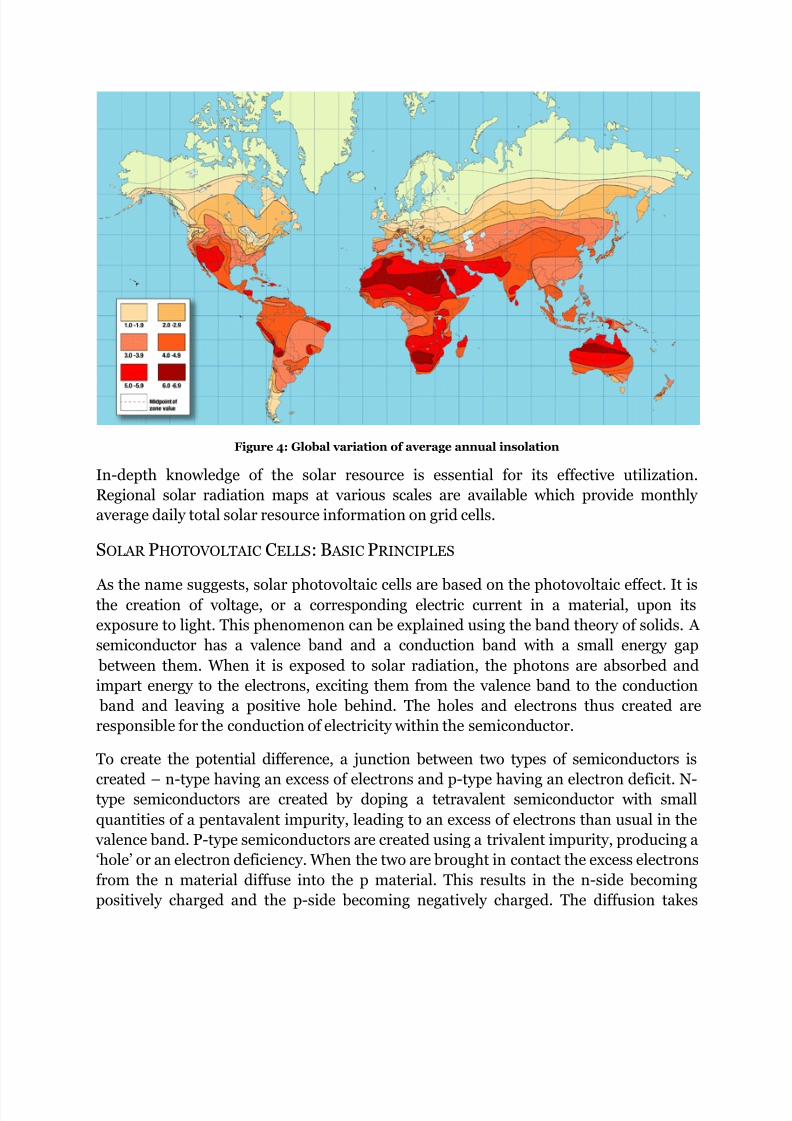
Figure 4: Global variation of average annual insolation
In-depth knowledge of the solar resource is essential for its effective utilization.
Regional solar radiation maps at various scales are available which provide monthly
average daily total solar resource information on grid cells.
SOLAR PHOTOVOLTAIC CELLS: B ASIC PRINCIPLES
As the name suggests, solar photovoltaic cells are based on the photovoltaic effect. It isthe creation of voltage, or a corresponding electric current in a material, upon its
exposure to light. This phenomenon can be explained using the band theory of solids. A
semiconductor has a valence band and a conduction band with a small energy gap
between them. When it is exposed to solar radiation, the photons are absorbed and
impart energy to the electrons, exciting them from the valence band to the conduction
band and leaving a positive hole behind. The holes and electrons thus created are
responsible for the conduction of electricity within the semiconductor.
To create the potential difference, a junction between two types of semiconductors is
created – n-type having an excess of electrons and p-type having an electron deficit. N-type semiconductors are created by doping a tetravalent semiconductor with small
quantities of a pentavalent impurity, leading to an excess of electrons than usual in the
valence band. P-type semiconductors are created using a trivalent impurity, producing a
„hole‟ or an electron deficiency. When the two are brought in contact the excess electrons
from the n material diffuse into the p material. This results in the n-side becoming
positively charged and the p-side becoming negatively charged. The diffusion takes
8/3/2019 Design and Engineering of Solar Photo Voltaic Cells
http://slidepdf.com/reader/full/design-and-engineering-of-solar-photo-voltaic-cells 5/15
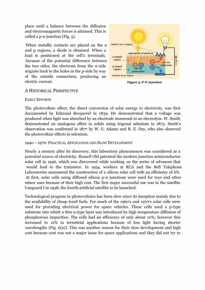
place until a balance between the diffusion
and electromagnetic forces is attained. This is
called a p-n junction (Fig. 5).
When metallic contacts are placed on the n
and p regions, a diode is obtained. When aload is positioned at the cell‟s terminals,
because of the potential difference between
the two sides, the electrons from the n-side
migrate back to the holes in the p-side by way
of the outside connection, producing an
electric current.
A HISTORICAL PERSPECTIVE
E ARLY
EFFORTS
The photovoltaic effect, the direct conversion of solar energy to electricity, was first
documented by Edmond Becquerel in 1839. He demonstrated that a voltage was
produced when light was absorbed by an electrode immersed in an electrolyte. W. Smith
demonstrated an analogous effect in solids using trigonal selenium in 1873. Smith's
observation was confirmed in 1877 by W. G. Adams and R. E. Day, who also observed
the photovoltaic effects in selenium.
1940 – 1970: PRACTICAL A PPLICATION AND SLOW DEVELOPMENT
Nearly a century after its discovery, this laboratory phenomenon was considered as apotential source of electricity. Russell Ohl patented the modern junction semiconductor
solar cell in 1946, which was discovered while working on the series of advances that
would lead to the transistor. In 1954, workers at RCA and the Bell Telephone
Laboratories announced the construction of a silicon solar cell with an efficiency of 6%.
At first, solar cells using diffused silicon p-n junctions were used for toys and other
minor uses because of their high cost. The first major successful use was in the satellite
Vanguard I in 1958, the fourth artificial satellite to be launched.
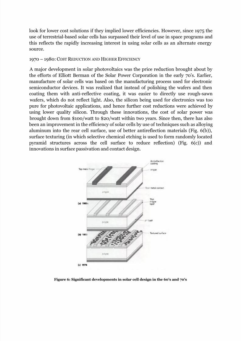
Technological progress in photovoltaics has been slow since its inception mainly due to
the availability of cheap fossil fuels. For much of the 1960's and 1970's solar cells wereused for providing electrical power for space vehicles. These cells used a p-type
substrate into which a thin n-type layer was introduced by high temperature diffusion of
phosphorous impurities. The cells had an efficiency of only about 10%; however this
increased to 12% in terrestrial applications because of less light having shorter
wavelengths (Fig. 6(a)). This was another reason for their slow development and high
cost because cost was not a major issue for space applications and they did not try to
Figure 5: P-N Junction
8/3/2019 Design and Engineering of Solar Photo Voltaic Cells
http://slidepdf.com/reader/full/design-and-engineering-of-solar-photo-voltaic-cells 6/15
look for lower cost solutions if they implied lower efficiencies. However, since 1975 the
use of terrestrial-based solar cells has surpassed their level of use in space programs and
this reflects the rapidly increasing interest in using solar cells as an alternate energy
source.
1970 – 1980: COST R EDUCTION AND HIGHER EFFICIENCY
A major development in solar photovoltaics was the price reduction brought about by
the efforts of Elliott Berman of the Solar Power Corporation in the early 70‟s. Earlier,
manufacture of solar cells was based on the manufacturing process used for electronic
semiconductor devices. It was realized that instead of polishing the wafers and then
coating them with anti-reflective coating, it was easier to directly use rough-sawn
wafers, which do not reflect light. Also, the silicon being used for electronics was too
pure for photovoltaic applications, and hence further cost reductions were achieved by
using lower quality silicon. Through these innovations, the cost of solar power was
brought down from $100/watt to $20/watt within two years. Since then, there has also been an improvement in the efficiency of solar cells by use of techniques such as alloying
aluminum into the rear cell surface, use of better antireflection materials (Fig. 6(b)),
surface texturing (in which selective chemical etching is used to form randomly located
pyramid structures across the cell surface to reduce reflection) (Fig. 6(c)) and
innovations in surface passivation and contact design.
Figure 6: Significant developments in solar cell design in the 60's and 70's

8/3/2019 Design and Engineering of Solar Photo Voltaic Cells
http://slidepdf.com/reader/full/design-and-engineering-of-solar-photo-voltaic-cells 7/15
1980 – 1990: THE EMERGENCE OF THIN-FILM TECHNOLOGY
There have been recent developments in
photovoltaic technology with the emergence
of thin-film solar cells (TFSCs). The first
TFSC having efficiency exceeding 10% wasproduced in 1980 at The Institute of Energy
Conversion at University of Delaware. A
thin-film solar cell, also called a thin-film
photovoltaic cell (TFPV), is a solar cell that is
made by depositing one or more thin films of
amorphous photovoltaic material on a
substrate (Fig. 7). The thickness range of
such a layer is wide and varies from a few
nanometers to tens of micrometers. Eventhough the efficiency of such solar cells is
lower than silicon-wafer cells, they are much more economical, lightweight, durable and
easy to use. However, they are still not being used in large scale commercial applications
due to lower efficiency and larger area requirement per watt produced.
1990 – PRESENT: COST VS. EFFICIENCY
Another major change has been the introduction of polycrystalline silicon or polysilicon
for solar cells in the late 90‟s. It is a material consisting of small silicon crystals, which
can be recognized by a visible grain, a “metal flake effect”. This material has less
efficiency, but is less expensive to produce in bulk. For the first time, in 2006, over half of the world's supply of polysilicon is being used for production of renewable electricity
solar power panels.
However, the highest efficiencies achieved so far for any photovoltaic technology have
been those for multi-junction solar cells. In 2008, scientists at the U.S. Department of
Energy's National Renewable Energy Laboratory (NREL) set a world record in solar cell
efficiency with an inverted metamorphic triple-junction solar cell that converts 40.8
percent of incident light into electricity.
Figure 7: Structure of a thin-film solar cell

8/3/2019 Design and Engineering of Solar Photo Voltaic Cells
http://slidepdf.com/reader/full/design-and-engineering-of-solar-photo-voltaic-cells 8/15
ENGINEERING A SPECTS OF SOLAR PHOTOVOLTAICS
MONOCRYSTALLINE SILICON W AFER CELLS AND SOLAR MODULES
Because the voltage of an individual silicon wafer solar cell is quite small (typically a
maximum voltage of 0.7V, with maximum power produced at 0.4V), a number of cellsare connected together to form a solar panel (or module), the number and arrangement
of cells depending on the application and required output. These cells sit on a tough
backing plate, while the grid of electrical connections lies above and below the surface of
the cells. The wafer has a full area metal contact made on the back surface, and a grid-
like metal contact made up of fine "fingers" and larger "busbars" are screen-printed onto
the front surface using a silver paste. The rear contact is also formed by screen-printing
a metal paste, typically aluminium. Usually this contact covers the entire rear side of the
cell, though in some cell designs it is printed in a grid pattern. The paste is then fired at
several hundred degrees celsius to form metal electrodes in ohmic contact with the
silicon. Some companies use an additional electro-plating step to increase the cellefficiency.
After the metal contacts are made, the solar cells are interconnected in series (and/or
parallel) by flat wires or metal ribbons, and assembled into modules. Electrical
connecting strips go from the bottom of one cell to the top of the next, connecting cells
in series. The connections are made in series to achieve the desired output voltage and
in parallel to achieve the desired current. The cells are connected to each other and to
the rest of the system using thin strips which may contain silver, copper or other
conductive but non-magnetic transition metals.
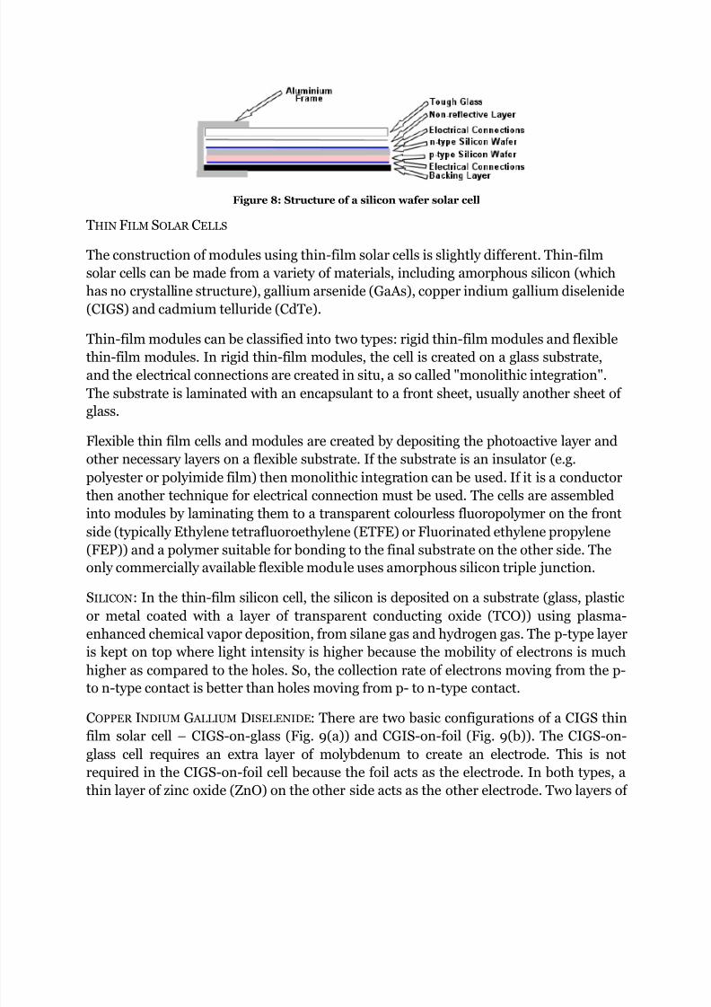
Over this is a non reflective layer (silicon is naturally reflective), to increase light
absorption. Silicon nitride has gradually replaced titanium dioxide as the antireflection
coating because of its excellent surface passivation qualities. It prevents carrier
recombination at the surface of the solar cell. It is typically applied in a layer several
hundred nanometers thick using plasma-enhanced chemical vapor deposition (PECVD).
Some solar cells have textured front surfaces that, like antireflection coatings, serve to
increase the amount of light coupled into the cell. Such surfaces can usually only be
formed on single-crystal silicon, though in recent years methods of forming them on
multicrystalline silicon have been developed. Finally on top will be a layer of tough
tempered glass, and the whole structure is usually within an aluminum frame, sealedagainst the weather (Fig. 8).
8/3/2019 Design and Engineering of Solar Photo Voltaic Cells
http://slidepdf.com/reader/full/design-and-engineering-of-solar-photo-voltaic-cells 9/15
Figure 8: Structure of a silicon wafer solar cell
THIN FILM SOLAR CELLS
The construction of modules using thin-film solar cells is slightly different. Thin-film
solar cells can be made from a variety of materials, including amorphous silicon (which
has no crystalline structure), gallium arsenide (GaAs), copper indium gallium diselenide
(CIGS) and cadmium telluride (CdTe).
Thin-film modules can be classified into two types: rigid thin-film modules and flexible
thin-film modules. In rigid thin-film modules, the cell is created on a glass substrate,and the electrical connections are created in situ, a so called "monolithic integration".
The substrate is laminated with an encapsulant to a front sheet, usually another sheet of
glass.
Flexible thin film cells and modules are created by depositing the photoactive layer and
other necessary layers on a flexible substrate. If the substrate is an insulator (e.g.
polyester or polyimide film) then monolithic integration can be used. If it is a conductor
then another technique for electrical connection must be used. The cells are assembled
into modules by laminating them to a transparent colourless fluoropolymer on the front
side (typically Ethylene tetrafluoroethylene (ETFE) or Fluorinated ethylene propylene(FEP)) and a polymer suitable for bonding to the final substrate on the other side. The
only commercially available flexible module uses amorphous silicon triple junction.
SILICON: In the thin-film silicon cell, the silicon is deposited on a substrate (glass, plastic
or metal coated with a layer of transparent conducting oxide (TCO)) using plasma-
enhanced chemical vapor deposition, from silane gas and hydrogen gas. The p-type layer
is kept on top where light intensity is higher because the mobility of electrons is much
higher as compared to the holes. So, the collection rate of electrons moving from the p-
to n-type contact is better than holes moving from p- to n-type contact.
COPPER INDIUM G ALLIUM DISELENIDE: There are two basic configurations of a CIGS thin
film solar cell – CIGS-on-glass (Fig. 9(a)) and CGIS-on-foil (Fig. 9(b)). The CIGS-on-
glass cell requires an extra layer of molybdenum to create an electrode. This is not
required in the CIGS-on-foil cell because the foil acts as the electrode. In both types, a
thin layer of zinc oxide (ZnO) on the other side acts as the other electrode. Two layers of

8/3/2019 Design and Engineering of Solar Photo Voltaic Cells
http://slidepdf.com/reader/full/design-and-engineering-of-solar-photo-voltaic-cells 10/15
the semiconductor material and cadmium sulphide are sandwiched in between, and
these act as the n-side and p-side of the solar cell respectively.
Figure 9(a): CGIS-on-glass, (b): CGIS-on-foil
C ADMIUM TELLURIDE: The CdTe solar cell has a similar structure. One electrode is made
from a layer of carbon paste infused with copper, the other from tin oxide (SnO2) or
cadmium stannate (Cd2SnO4). The semiconductor in this case is cadmium telluride
(CdTe), which, along with cadmium sulfide (CdS), creates the n-type and p-type layers
required for the PV cell to function.
MULTI-JUNCTION SOLAR CELLS
Multi-junction cells use two or more layers of different materials with different band
gaps. The main motivation behind this is the fact that conventional photovoltaic cells
are unable to extract all the energy from a photon, and that they cannot extract any
energy at all from photons of certain wavelengths. If the photon has less energy than the
bandgap, it is not collected at all. This is a major consideration for conventional solar
cells, which are not sensitive to most of the infrared spectrum, although that represents
almost half of the power coming from the sun. Conversely, photons with more energy
than the bandgap, say blue light, initially eject a photon with much more energy than
the bandgap, but this extra energy is lost through a process known as "relaxation". This
lost energy turns into heat in the cell, which has the side-effect of further increasing blackbody losses. This problem limits the theoretical maximum efficiency of solar cells
to about 34%.
This problem is overcome in multi-junction solar cells by having more than one junction
with different band gaps. Depending on the substance, photons of varying energies are
absorbed. So by stacking higher band gap material on the surface to absorb high-energy
photons, while allowing lower-energy photons to be absorbed by the lower band gap

8/3/2019 Design and Engineering of Solar Photo Voltaic Cells
http://slidepdf.com/reader/full/design-and-engineering-of-solar-photo-voltaic-cells 11/15
material beneath, much higher efficiencies can be attained. Theoretically, a solar cell
having infinite number of junctions can have efficiency as high as 87%. Commercial
samples having efficiency up to 30% are now available.
The majority of multi-junction cells that have been produced to date use three layers,
tuned to blue (on top), yellow and red (on the bottom). These cells require the use of semiconductors that can be tuned to specific frequencies, which has led to most of them
being made of gallium arsenide (GaAs) compounds, often germanium for red, GaAs for
yellow, and GaInP2 for blue. To date, their higher price and lower price-to-performance
ratio have limited their use to special roles, notably in aerospace where their high
power-to-weight ratio is desirable. The cost is mainly due to the complex structure and
the high pice of materials. In terrestrial applications these solar cells are used in
concentrated photovoltaics (CPV) with operating plants all over the world.
Table 1 shows a comparison of the different photovoltaic technologies available, with Fig
10 showing the relative market share for each.
Technology η (%) V OC (V) I SC (A) W/m² t (µm)
u c-Si 24.7 0.5 0.8 63 100
p c-Si 20.3 0.615 8.35 211 200
a-Si 11.1 6.3 0.0089 33 1
CdTe 16.5 0.86 0.029 – 5
CIGS 19.5 – – – 1
MJ 40.7 2.6 1.81 476 140
Table 1: Performance characteristics of different photovoltaic technologies
Figure 10: Relative market share for different photovoltaic technologies

8/3/2019 Design and Engineering of Solar Photo Voltaic Cells
http://slidepdf.com/reader/full/design-and-engineering-of-solar-photo-voltaic-cells 12/15
Once the solar cells have been linked together to form solar modules, these are further
linked together to form a collection known as a solar array. The connections are made a
rationale similar to that followed for the connections among individual cells – they are
connected in series to achieve the desired voltage (each such set in series is called a
„string‟) and the individual strings are connected in parallel to allow the system to
produce more current.
B ALANCE OF S YSTEM
The balance of system or BOS includes all components of the solar system apart from
the solar modules. This includes the battery (in the case of off-grid installations), the
control unit and the inverter, the mechanical support structure, the electric cabling, and
protection devices such as fuses, grounding rods, and disconnect switches. Fig. 11
illustrates the costs incurred in the various components of a photovoltaic installation
with storage.
Figure 11: Cost breakup of a photovoltaic installation with storage
B ATTERIES: Photovoltaic systems can be broadly divided into two types – standalone
systems and grid-connected systems. Grid connected systems vary in size from
residential (2-10kWp) to solar power stations (up to 10s of GWp). Standalone systems
vary in scale and application from toys and calculators to buildings and space stations.
In many cases such as PV-powered pumps batteries are not required as water can be
pumped and stored during sunlight hours. If power is to be supplied independent of
solar insolation, it has to be stored using batteries. These comprise a significant portion
of the cost of a photovoltaic system, especially over the course of its life cycle because
batteries need to be replaced every four to eight years due to their relatively short
lifetime.
In most cases, lead-acid batteries are used because of their low cost. While automobile
batteries are optimized for providing strong current for a short period to start the car,
the ideal batteries for PV systems are so-called “deep cycle” batteries that can yield a
large fraction of their charge (deep discharge cycle) and must operate with high

8/3/2019 Design and Engineering of Solar Photo Voltaic Cells
http://slidepdf.com/reader/full/design-and-engineering-of-solar-photo-voltaic-cells 13/15
efficiency and long duration. Yet, many PV applications use standard “shallow
discharge” auto batteries due to their ubiquitous availability and lower initial cost. Some
of the modern batteries such as those based on lithium ion or lithium polymer used in
laptop computers or mobile phones could be used in solar applications but they are too
expensive and are not significantly better than properly managed lead-acid batteries.
Alternative methods of storage exist but they will not replace lead-acid battery, at least,not in the next ten years.
INVERTER : The next requirement is an inverter, which converts the DC produced by the
photovoltaic module into AC. For large photovoltaic plants, this may either be a
centralized inverter, which is theoretically cheaper, or one may have a solar micro-
inverter on the back of every module, which increases the reliability of the system. The
inverter has an additional and important role: to vary the electrical operating point of
the PV array to maintain its output at the maximum value. Changes of temperature and
insolation change the voltage where maximum power extraction occurs, so the
electronics of the inverter typically include maximum power tracking.
TRACKING S YSTEM: To gather solar energy effectively, a solar panel should be within
about twenty degrees either side of perpendicular to the sun. An angle of more than
thirty-five degrees from the perpendicular results in a significant portion of sunlight
being reflected off the solar panel surface. In order to maximize the amount of solar
radiation incident on the solar modules, large photovoltaic installations that approach
or exceed one megawatt have tracking systems. These use optical sensors to track the
position of the sun and make sure that the panel is aimed directly at the sun or at the
brightest portion of a partially cloudy sky, improving the performance by upto 100%.
CONCENTRATED PHOTOVOLTAIC TECHNOLOGY
Solar cells may also be used along with solar radiation concentrating systems. This
offers two main advantages. The first is that since fewer solar cells are required to collect
the sunlight falling on a given area, higher cost technology can be used than in cases
where non-concentrated radiation is used to generate power, and therefore solar cells
having higher efficiency (such as multi-junction solar cells) can be used. The second is
that concentration of solar radiation enables more radiation per unit area to be incident
upon the solar cell, producing more power and hence reducing the area of the
photovoltaic cells, replacing it with less expensive optical material.
The concentrators used for this purpose can be either refractive or reflective. The lenses
used can have point focus, or may have a linear focus (Fig. 12(a)) and are usually made
of acrylic plastic (PMMA), which is much more durable than glass.

8/3/2019 Design and Engineering of Solar Photo Voltaic Cells
http://slidepdf.com/reader/full/design-and-engineering-of-solar-photo-voltaic-cells 14/15
Figure 12(a): Refractive concentrators, (b): Reflective concentrators
Reflective concentrators use parabolic mirrors to concentrate sunlight from a large area
onto a single point or along a line (Fig. 12(b)).
Most concentrated photovoltaic applications use some kind of tracking mechanism to
maximize the amount of solar power being concentrated. With point concentration, two-
axis tracking is required, which is more difficult and expensive. However, they are able
to achieve a higher concentration ratio, reducing the cost of the solar cells. With linear
concentrators, one axis tracking can be used, which is less expensive but concentrates
the solar radiation over a larger area.
For high concentration ratios, the module also requires cooling systems because the
efficiency of solar cells deteriorates at higher temperatures. This further increases the
cost of the system, making it suitable for only large scale applications. So, before
installing any such system, there needs to be an in depth analysis of the improvements
in cost and efficiency achieved by using higher levels of concentration versus the
additional costs and complexities involved in doing the same.

8/3/2019 Design and Engineering of Solar Photo Voltaic Cells
http://slidepdf.com/reader/full/design-and-engineering-of-solar-photo-voltaic-cells 15/15
R EFERENCES
Renewable energy: sources for fuels and electricity, T. B. Johansson, H. Kelly, A. K. N. Reddy, R.
H. Williams, L. Burnham (eds.), Island Press (1993)
Handbook of Photovoltaic Science and Engineering, A. Luque, S. Hegedus (eds.), John Wiley
and Sons Ltd., UK (2003)
A Guide to Photovoltaic (PV) System Design and Installation, California Energy Commission,
June 2001, 500-01-020
C. D. Mickey, Solar Photovoltaic Cells (1981), Journal of Chemical Education, Vol. 58 No. 5 pp.
418-423
A. G. Aberle, Thin Film Solar Cells (2009), Thin Solid Films, Vol. 517, Issue 17 pp. 4706-4710
http://www.eoearth.org/article/Solar_radiation (accessed 29th October 2011)
http://www.nrel.gov/gis/solar.html (accessed 29th October 2011)
http://photovoltaics.sandia.gov/docs/PVFEffIntroduction.htm (accessed 31st October 2011)
http://www.solar-facts.com/panels/panel-construction.php (accessed 31st October 2011)
http://science.howstuffworks.com/environmental/green-science/thin-film-solar-cell.htm
(accessed 31st October 2011)
http://www.nrel.gov/csp/concentrating_pv.html (accessed 31st October 2011)
http://en.wikipedia.org/wiki/Photovoltaics (accessed 31st October 2011)
http://en.wikipedia.org/wiki/Solar_cell (accessed 29th October 2011)
http://en.wikipedia.org/wiki/Solar_panel (accessed 31st October 2011)
http://en.wikipedia.org/wiki/Thin_film_solar_cell (accessed 31st October 2011)
http://en.wikipedia.org/wiki/Multijunction_photovoltaic_cell (accessed 31st October 2011)
http://en.wikipedia.org/wiki/Concentrated_photovoltaics (accessed 5th November 2011)