design and fabrication of imperfection-immune carbon ...my460fq1046/phddissert_v24... · design and...
TRANSCRIPT

DESIGN AND FABRICATION OF
IMPERFECTION-IMMUNE
CARBON NANOTUBE DIGITAL VLSI CIRCUITS
A DISSERTATION
SUBMITTED TO THE DEPARTMENT OF ELECTRICAL ENGINEERING
AND THE COMMITTEE ON GRADUATE STUDIES
OF STANFORD UNIVERSITY
IN PARTIAL FULFILLMENT OF THE REQUIREMENTS FOR THE DEGREE OF
DOCTOR OF PHILOSOPHY
Nishant Patil
April 2010

http://creativecommons.org/licenses/by-nc/3.0/us/
This dissertation is online at: http://purl.stanford.edu/my460fq1046
© 2010 by Nishant Parag Patil. All Rights Reserved.
Re-distributed by Stanford University under license with the author.
This work is licensed under a Creative Commons Attribution-Noncommercial 3.0 United States License.
ii

I certify that I have read this dissertation and that, in my opinion, it is fully adequatein scope and quality as a dissertation for the degree of Doctor of Philosophy.
Subhasish Mitra, Primary Adviser
I certify that I have read this dissertation and that, in my opinion, it is fully adequatein scope and quality as a dissertation for the degree of Doctor of Philosophy.
Christoforos Kozyrakis
I certify that I have read this dissertation and that, in my opinion, it is fully adequatein scope and quality as a dissertation for the degree of Doctor of Philosophy.
Philip Wong
Approved for the Stanford University Committee on Graduate Studies.
Patricia J. Gumport, Vice Provost Graduate Education
This signature page was generated electronically upon submission of this dissertation in electronic format. An original signed hard copy of the signature page is on file inUniversity Archives.
iii
iv
Abstract
Carbon Nanotube Field Effect Transistors (CNFETs), consisting of
semiconducting single walled Carbon Nanotubes (CNTs), show great promise as
extensions to silicon CMOS. While there has been significant progress at a single-device
level, a major gap exists between such results and their transformation into VLSI CNFET
technologies. Major CNFET technology challenges include mis-positioned CNTs,
metallic CNTs, and wafer-scale integration. This work presents design and processing
techniques to overcome these challenges. Experimental results demonstrate the
effectiveness of the presented techniques.
Mis-positioned CNTs can result in incorrect logic functionality of CNFET
circuits. A new layout design technique produces CNFET circuits implementing arbitrary
logic functions that are immune to a large number of mis-positioned CNTs. This
technique is significantly more efficient compared to traditional defect- and fault-
tolerance. Furthermore, it is VLSI-compatible and does not require changes to existing
VLSI design and manufacturing flows.
A CNT can be semiconducting or metallic depending upon the arrangement of
carbon atoms. Typical CNT synthesis techniques yield ~33% metallic CNTs. Metallic
CNTs create source-drain shorts in CNFETs resulting in excessive leakage (Ion/Ioff < 5)
and highly degraded noise margins. A new technique, VLSI-compatible Metallic-CNT
Removal (VMR), overcomes metallic CNT challenges by combining layout design with

v
CNFET processing. VMR produces CNFET circuits with Ion/Ioff in the range of 103-10
5,
and overcomes the limitations of existing metallic-CNT removal techniques.
The above techniques are demonstrated for complex logic structures using wafer-
scale growth of (99.5%, estimated from Scanning Electron Micrographs) aligned CNTs
on single-crystal quartz and wafer-scale CNT transfer from quartz to silicon. Such an
integrated approach enables the first experimental demonstration of VLSI-compatible
CNFET combinational circuits (e.g., computational elements such as half-adder sum-
generators) and storage circuits (e.g., sequential elements such as D-latches) that are
immune to inherent CNT imperfections. These experimentally-demonstrated circuits
form essential building blocks for large-scale digital computing systems.

vi
Acknowledgments
I would like to thank my thesis advisor, Professor Subhasish Mitra for invaluable
guidance and advice, without which this work would not have been possible. I greatly
appreciate his close involvement in working with me to develop new research ideas,
writing papers and polishing my presentations. I would also like to thank Professor H. –S.
Philip Wong for being my associate advisor and providing direction and guidance to the
experimental part of my thesis work. I would also acknowledge Professor Christos
Kozyrakis for being on my thesis committee and Professor Zhenan Bao for chairing my
oral defense committee.
I was very fortunate to work with great collaborators including Deji Akinwande,
Kyle Anderson, Alexander Badmaev, Cara Beasley, Chen Chen, Hong-yu (Henry) Chen,
Xiangyu (Helen) Chen, Arash Hazeghi, Dr. Edward Myers, Koungmin Ryu and Gordon
Wan, Haowei Zhang. I would especially like to thank Jie Deng, Albert Lin, Hai Wei and
Jie (Jerry) Zhang, with whom I had very close and fruitful collaborations. A special
acknowledgement goes to Dr. James McVittie, who worked closely with me to modify
lab equipment and make sure it functioned well. I would also like to thank both the staff
members and other lab members of the Stanford Nanofabrication Facility (SNF). I would
also like to thank Professor Yoshio Nishi for allowing me to use his PECVD furnace.
I would like to thank members of the Robust Systems Group and also Uma
Mulukutla for all her support in administrative matters.

vii
I would like to thank my family for all their support and opportunities they have
given me through the years and my friends for making my stay at Stanford enjoyable.
My studies at Stanford were supported by the Art and Mary Fong Stanford
Graduate Fellowship, Stanford School of Engineering Fellowship, FCRP C2S2, FCRP
FENA and the National Science Foundation. The work presented in this thesis was done
partly in the Stanford Nanofabrication Facility (SNF) of the National Nanotechnology
Infrastructure Network (NNIN).

viii
Table of Contents
List of Tables ...................................................................................................................... x
List of Figures .................................................................................................................... xi
Chapter 1: Introduction ........................................................................................................1
1.1 Background ..............................................................................................................1
1.2 Contributions............................................................................................................4
1.3 Outline......................................................................................................................5
Chapter 2: Mis-positioned-Carbon-Nanotube-Immune Design...........................................7
2.1 Determining Vulnerability to Mis-positioned CNTs ...............................................8
2.2 Sufficient Condition for Mis-positioned-CNT-Immune Design ...........................17
2.3 Simulation Results .................................................................................................21
Chapter 3: Wafer-Scale Carbon Nanotube Growth and Transfer and Fabrication of
Mis-positioned-CNT-Immune Logic Structures..........................................................25
3.1 Wafer-scale CNT Growth ......................................................................................25
3.2 CNT Growth Characterization...............................................................................31
3.3 Wafer-scale CNT Transfer.....................................................................................33
3.4 CNFET Characterization .......................................................................................36
3.5 Fabrication of Mis-positioned-CNT-Immune Logic Structures ............................38
Chapter 4: VMR: VLSI-Compatible Metallic CNT Removal...........................................43
4.1 Existing m-CNT Removal Techniques..................................................................44
4.2 VMR Technique and Experimental Results ..........................................................45
4.3 VMR Scalability ....................................................................................................53
ix
Chapter 5: VLSI-Compatible Combinational and Sequential CNFET Circuits ................58
5.1 CNFET Circuit Elements.......................................................................................58
5.2 CNFET Combinational Circuits ............................................................................60
5.3 CNFET Sequential Circuits ...................................................................................63
Chapter 6: Concluding Remarks........................................................................................65
Appendix: Fabrication Details ...........................................................................................69
A.1 Carbon Nanotube Growth .....................................................................................69
A.2 Carbon Nanotube Transfer....................................................................................74
A.3 CNFET Circuit Fabrication...................................................................................75
Publications........................................................................................................................78
References..........................................................................................................................84

x
List of Tables
Table 2.1. Labels associated with nodes in the graph. .............................................11
Table 2.2. Penalties for mis-positioned-CNT-immune design. ................................24
Table 6.1. CNFET Technology Challenges and Outlook..........................................66
Table A.1. Annealing Schedule for Quartz Wafers ....................................................69
xi
List of Figures
Figure 1.1. Carbon Nanotube Field Effect Transistor..................................................2
Figure 1.2. CNFET Inverter. ............................................................................................3
Figure 2.1. Incorrect Logic Functionality caused by mis-positioned CNTs..............8
Figure 2.2. (a) Mis-positioned-CNT-vulnerable NAND. (b) Mis-positioned-
CNT-immune NAND. ....................................................................................10
Figure 2.3. Grid Decomposition of NAND cell layouts in Fig. 2.2............................12
Figure 2.4. Graph representations of NAND cell layouts in Fig. 2.3. ......................12
Figure 2.5. Reduced graphs for NAND cell layouts in Fig. 2.4. ...............................13
Figure 2.6. Traversal of NAND cell graphs in Fig. 2.5. .............................................16
Figure 2.7. Mis-positioned-CNT-immune layout for a network specified in
Sum of Products Form. ................................................................................18
Figure 2.8. Mis-positioned-CNT-immune layout for a network specified in
Product of Sums Form. ................................................................................19
Figure 2.9. Mis-positioned-CNT-immune layout for network represented by
the function A+(B+C) (D+E). .......................................................................20
Figure 2.10. Steps to create mis-positioned CNT immune layout of Fig. 2.9........21
Figure 2.11. Misaligned-and-mis-positioned-CNT-vulnerable NAND3 (a) and
AOI21 (b). .......................................................................................................23
Figure 2.12. Mis-positioned-CNT-immune NAND3 (a) and AOI21 (b). ..................23
Figure 3.1. Wafer-scale aligned CNT growth process. .............................................28
Figure 3.2. Wafer-scale aligned CNT growth using stripped Fe catalyst. ..............30
Figure 3.3. Effect of catalyst width (W) and spacing (S) on CNT density and
CNT coverage. (a) W = 10 µm, S = 1200 µm. (Length of longest
CNT in image = 675 µm). (b) W = 0.5 µm, S = 50 µm. (c) W = 0.5
µm, S = 100 µm. (d) W = 1 µm, S = 50 µm. (e) W = 2 µm, S = 50
µm. (f) W = 4 µm, S = 50 µm. (g) W = 1 µm, S = 100 µm. (h) W = 2
xii
µm, S = 100 µm. (i) W = 4 µm, S = 100 µm. (j) W = 1 µm, S = 200
µm. (k) W = 2 µm, S = 200 µm. (l) W = 4 µm, S = 200 µm.....................31
Figure 3.4 (a) AFM image of aligned CNTs on quartz. (b) CNT diameter
distribution. .....................................................................................................32
Figure 3.5 (a) Optical micrograph of 4” ST-cut quartz wafer after aligned
CNTs growth and subsequent patterning of contacts. (b) SEM
Image of aligned CNTs bridging two contacts (c) Two terminal
measurement parameters............................................................................33
Figure 3.6. Two terminal current distributions at 1V bias for n functional
devices (out of 18) (Width = 50 µm, Length = 1 µm) in 5 arbitrary
dies (out of 197 dies on the wafer) over 5 regions of the quartz
wafer................................................................................................................33
Figure 3.7. SEM images of transferred CNTs. ...........................................................34
Figure 3.8. CNT transfer technique..............................................................................35
Figure 3.9. CNFET Current distributions (Vds = 1V Vgs = -5V) of 18 back-gated
CNFETs (W = 50 µm, L = 1 µm, tSiO2=50 nm, Ti(5 nm)/Au(50 nm)
contacts) in 5 regions of the silicon wafer. ................................................38
Figure 3.10. Mis-positioned-CNT-immune CNFET circuits (a) Cross-section of
CNFET. (b) SEM of fabricated CNFET. (c) Mis-positioned-CNT-
immune NAND pull-up before etching. (d) Mis-positioned-CNT-
immune NAND pull-up after etching. .........................................................40
Figure 3.11. Experimental demonstration of Mis-positioned-CNT-immune
logic structures. SEM images of Logic structures corresponding to
(a) NAND pull-up (b) NOR pull-up (c) AND-OR-INVERT pull-up (d)
OR-AND-INVERT pull-up.............................................................................41
Figure 3.12 Experimental demonstration of correct logic behavior of mis-
positioned-CNT-immune NAND (a) and NOR (b) pull-up logic
structures........................................................................................................42
Figure 4.1. Incorrect logic functionality due to m-CNT fragments left behind
after Single Device Breakdown (SDB)......................................................45

xiii
Figure 4.2. Optical micrographs and illustrations of VMR process steps. .............46
Figure 4.3. Top view (a) and cross-sectional view (b) of VMR structure
consisting of 6 inter-digitated VMR electrodes. (c) SEM Image of
VMR structure (top view). ............................................................................48
Figure 4.4. VMR example for an arbitrary final design..............................................49
Figure 4.5 (a) Electrical breakdown of metallic CNTs (m-CNTs) using a back-
gated VMR structure. (b) Typical current-voltage (IDS-VGS)
characteristics for a VMR structure at different points during the m-
CNT breakdown process. VDS = -1V. ........................................................50
Figure 4.6. Ion vs. Ion / Ioff for 104 VMR structures with 7, 13, 21, 25 inter-
digitated VMR electrodes. VMR electrode width = 50 µm. Average
s-CNT current yield, defined as (Ion–Ioff)After_VMR / (Ion–Ioff)Before_VMR, is
95%. Ion is measured at VGS = -5V. Ioff is measured at VGS = 40V.
High back-gate voltage is needed because of the thick back-gate
oxide (100 nm SiO2). ....................................................................................51
Figure 4.7. Layout modifications needed for VMR. (a) NAND layout with
added contacts (marked with black circle). (b) Multiplexer layout
with added contacts (marked with black circles)......................................52
Figure 4.8. Typical current-voltage characteristics (a) IDS-VGS (VDS = -1V) (b)
IDS-VDS (VGS step = 1V) of a multiple-CNT CNFET (Width = 50 µm,
Length = 1 µm, Number of CNTs = ~100) after VMR and fabrication
of top-gate oxide (12 nm HfO2) and top-gate metal: bilayer of
Titanium (2 nm) and Platinum (25 nm). The threshold voltage of the
CNFETs is negative (enhancement-mode p-type CNFETs) enabling
CNFET logic gates that can be cascaded.................................................53
Figure 4.9 Resistor network and schematic representing a VMR electrode.
Resistance of electrode section (Re) depends on the material used
for the electrodes and CNT density. Resistance of m-CNT (Rm) =
50kΩ. Resistance of s-CNT (off-state) Rs = 50MΩ..................................54

xiv
Figure 4.10. Voltage profile simulation of a VMR electrode (Palladium) with
10V applied at the two ends. Width of metal (Wmetal) = 100 nm (Fig.
4.9), Thickness of palladium VMR electrodes = 100 nm. CNT
density = 10 CNTs/µm. VDS,Breakdown of m-CNTs = 5V for CNT length
= 1 µm [Pop 08] (a) Width of VMR electrode = 62 µm. (b) Width of
VMR electrode = 55 µm. ..............................................................................55
Figure 4.11. Maximum width of VMR electrodes. ......................................................55
Figure 4.12. Area cost analysis for different metallic carbon nanotube removal
techniques. Compared with VMR, improved VMR reduces the
worst-case area overhead from 200+% down to 1% at the 22 nm
technology node. ...........................................................................................56
Figure 5.1 (a) Circuit elements used in final CNFET circuits– Multiplexer pull-
up, NAND pull-up and pull-down CNFET. (b) Scatter plot of Ion vs.
Ion/Ioff for the circuit elements fabricated with and without VMR. All
CNFETs have width = 50 µm and length = 1 µm. Ion for circuit
elements without VMR does not include m-CNT current (Ioff). Total
number of circuit elements measured = 81. All CNFET circuit
elements fabricated using VMR show high Ion/Ioff (103–105). Ion
decreases after VMR because some s-CNTs are removed during
VMR (see Fig. 4.5)........................................................................................59
Figure 5.2. Single-stage CNFET logic gates using VMR and all-PMOS logic
with pull-down CNFETs. (a) CNFET inverter. (b) CNFET NAND..........61
Figure 5.3. Experimental demonstration of multi-stage cascaded imperfection-
immune CNFET inverter chain (gain for inverter chain= 14)
fabricated in a VLSI-compatible manner. ..................................................62
Figure 5.4 (a) Scanning electron micrograph (SEM) of CNFET half-adder sum
generator implementing the equivalent of an XNOR function (left
panel). Scale bar represents 20 µm. SEM of aligned CNTs in
XNOR before top-gate metal deposition (right panel). Scale bar
represents 2 µm. (b) Circuit diagram and truth table for a half-adder

xv
sum generator. (c) Voltage transfer curves and gain for CNFET
half-adder sum generator. VBias = 4V. VDD = 3V.....................................63
Figure 5.5. (a) Scanning electron micrograph (SEM) of CNFET D-Latch (top
panel). Scale bar represents 20 µm. SEM of aligned CNTs in D-
Latch before top-gate metal deposition (bottom panel). Scale bar
represents 2 µm. (b) Circuit diagram for D-Latch. (c) D-Latch
checking experiments. Inputs to the D-Latch were manually
toggled. VBias = 5V. VDD = 3V.....................................................................64


- 1 -
Chapter 1: Introduction
1.1 Background
Energy efficiency is the most significant challenge for continued integration of
systems according to Moore’s law, the principal driver behind the semiconductor
industry. Carbon Nanotubes (CNTs) provide a very promising path towards solving this
outstanding challenge. CNTs are cylindrical nanostructures of carbon with exceptional
electrical, thermal, and mechanical properties [Saito 98]. CNTs with a single shell of
carbon atoms are called single-walled carbon nanotubes (SWNTs) and have diameters
between 0.5-3 nm (in this thesis, all CNTs are SWNTs). CNTs are grown through a
process of chemical synthesis [Dai 02]. A CNT can be metallic or semiconducting
depending upon the arrangement of carbon atoms in the CNTs (chirality) [Saito
98].Using semiconducting CNTs, we can create Carbon Nanotube Field Effect
Transistors (CNFETs) as shown in Fig. 1.1. Multiple semiconducting CNTs are grown or
deposited on an insulating substrate. The regions of the CNTs under the gate act as the
channel region of the CNFET. The conductivity of these channel regions is controlled by
the voltage applied at the gate similar to silicon MOSFETs. The regions of the CNTs
outside the gate are heavily doped and act as the source and drain regions of the CNFET.
Figure 1.2 shows the layout of a CNFET inverter. The gate, source and drain contacts,
and interconnects are defined by conventional lithography. The distances between gates
and contacts are limited by the lithographic feature size (lithographic pitch in Fig. 1.2,

- 2 -
e.g., 64 nm for 32 nm technology node). Since CNTs are grown using chemical synthesis,
the inter-CNT distance (sub-lithographic pitch in Fig. 1.2) is not limited by lithography.
CNFETs are excellent candidates for highly energy-efficient next-generation
integrated systems. A ‘perfect’ CNFET technology is predicted to be 5× faster than
silicon transistors, while consuming the same power
[Wei 09b]. However, several
significant challenges must be overcome before such benefits can be experimentally
realized.
Gate
Drain Contact
Source Contact
Substrate (e.g Quartz)Semiconducting CNT(Undoped Region)
Semiconducting CNT (Doped Region) Oxide
Gate
Drain Contact
Source Contact
Substrate (e.g Quartz)Semiconducting CNT(Undoped Region)
Semiconducting CNT (Doped Region) Oxide
Figure 1.1. Carbon Nanotube Field Effect Transistor.
There have been significant accomplishments in the scientific discovery of
CNFETs mainly at the single-CNT level. These include demonstrations of high-
performance CNFETs and single-CNT logic gates [Javey 03a, 03b, 05], single-CNT ring
oscillator [Chen 06], and percolation-transport-based CNT circuits on flexible substrates
[Cao 08]. Despite such accomplishments, major barriers must be overcome before these
material revolutions can be harnessed into technologies with practical impact on society.

- 3 -
Sub -lithographicPitch (4nm)
N+ doped
SemiconductingCNTs
for source & drain
VddContact*
Output Contact*
Gnd Contact*
Gate*Input*
P+ doped
Semiconducting
CNTs
for source & drain Lithographic Pitch (64nm = 4λ)
IntrinsicCNT region
Multiple aligned CNTs
* Lithographically defined gate and contacts
Interconnect
Figure 1.2. CNFET Inverter.
Two fundamental limitations inherent to CNTs are major obstacles to large-scale
integration of CNFET circuits:
1. It is nearly impossible to guarantee perfect alignment and accurate positioning
of all CNTs at the wafer-scale. Mis-positioned CNTs introduce stray conducting paths in
logic circuits causing incorrect functionality.
2. CNTs can be either metallic or semiconducting depending on their atomic
arrangement (chirality). Semiconducting CNTs are essential for CNFETs. Metallic CNTs
cause shorts inside CNFETs resulting in excessive leakage power and significantly
increased susceptibility to noise leading to incorrect functionality. No known CNT
synthesis techniques can produce exclusively semiconducting CNTs.
In spite of several unanswered questions about CNFETs, three major trends are
clear:

- 4 -
1) Future VLSI systems cannot rely solely on current chemical synthesis for
guaranteed perfect devices. As discussed before, mis-positioned CNTs can result in
incorrect logic functionality. Similarly, no known CNT growth technique guarantees 0%
m-CNTs. m-CNTs create source-drain shorts resulting in excessive leakage, severely
degraded noise margins, and delay variations.
2) Expensive defect- and fault-tolerance techniques will not enable wide adoption
of CNFET-based circuits. Expensive techniques can create major roadblocks to the
adoption of CNFET technologies.
3) New design techniques must be compatible with VLSI processing and have
minimal impact on existing VLSI design flows. Investments made in VLSI design
infrastructure are too large to be ignored. For example, techniques that rely on separate
customization of every chip can be prohibitively expensive if not designed carefully.
New design techniques, together with advances in CNT processing, must be
employed to create CNFET circuits that are immune to inherent CNT imperfections.
1.2 Contributions
We experimentally demonstrate imperfection-immune design techniques to
overcome the challenges of mis-positioned and metallic CNTs. The mis-positioned-CNT-
immune design technique ensures correct logic functionality even though all CNTs are
not perfectly aligned and positioned. Mis-positioned-CNT-immune design, together with
a new full-wafer-scale CNT growth and transfer technique, enables the first experimental

- 5 -
demonstration of full-wafer-scale CNFET digital logic structures immune to misaligned
and mis-positioned CNTs.
To overcome the metallic CNT challenge, we introduce another imperfection-
immune design technique called VLSI-compatible Metallic-CNT Removal (VMR) to
ensure that CNFET circuits continue to function correctly even though CNT synthesis
cannot guarantee absence of metallic CNTs.
Two salient features of these imperfection-immune design techniques are:
1. Minimal power, performance and area impact at the system-level. Hence, it
retains the energy efficiency benefits of CNFET circuits.
2. It is compatible with existing VLSI fabrication methods. This property is
essential for enabling future CNFET VLSI.
Using the imperfection-immune design approach, we were able to demonstrate,
for the first time, CNFET combinational circuits (e.g., computational elements such as
half-adder sum-generators) and storage circuits (e.g., sequential elements such as D-
latches), which form essential components of CNFET digital VLSI circuits.
1.3 Outline
Chapter 2 describes mis-positioned-CNT-immune design. Chapter 3 presents
experimental demonstration of wafer-scale CNT growth and transfer and fabrication of
mis-positioned-CNT-immune logic structures. Chapter 4 introduces a VLSI-compatible

- 6 -
Metallic CNT Removal technique called VMR and presents experimental results and
analysis of this technique. Chapter 5 presents experimental demonstration of CNFET
combinational and sequential circuits fabricated using the aforementioned imperfection-
immune design techniques such as mis-positioned-CNT-immune design and VMR.

- 7 -
Chapter 2: Mis-positioned-Carbon-Nanotube-Immune Design
© [2008] IEEE. Part of this chapter has been reproduced with permission from N.
Patil et al., “Design Methods for Misaligned and Mis-positioned Carbon-Nanotube-
Immune Circuits”, IEEE Transactions on Computer-Aided Design of Integrated Circuits
and Systems, vol. 27, no. 10, pp. 1725-1736, 2008.
A mis-positioned CNT is a CNT that passes through a layout region where a CNT
was not intended to pass. This may be caused due to misalignment or due to lack of
control of correct positioning of CNTs during CNT growth. A large fraction (99.5%) of
the CNTs grown on single-crystal quartz substrates grow aligned i.e. straight and parallel
to each other [Kang 07]. Even for CNTs on quartz substrates, a non-negligible fraction of
CNTs are misaligned. It is very difficult to correctly position and align all the CNTs for
all CNFETs for VLSI. Mis-positioned CNTs can cause shorts and incorrect logic
functionality in CNFET logic circuits (Fig. 2.1). Using design principles described in
[Patil 07, 08b] we experimentally demonstrated in [Patil 08a, 08b] circuits that are
immune to a large number of mis-positioned CNTs. We refer to these circuits as mis-
positioned-CNT-immune circuits. This is accomplished by etching CNTs from regions
pre-defined during layout design, so that any mis-positioned CNT cannot result in
incorrect logic functionality. This technique is VLSI-compatible since it does not require
any die-specific customization or test and reconfiguration. All logic cells have CNTs

- 8 -
removed in the predefined layout regions using oxygen plasma [Patil 08a, 08b]. This is
feasible since the penalties associated with this technique are small.
A
B
A
B
Vdd
Gnd
Pull-up
Wanted: A′ + B′
Got: Short
Pull-up
Wanted: A′ + B′
Got: Short
Out
Mis-positionedCNT outside gate
Ion / Ioff ratio can be severely degraded
Pull-downMis-positioned CNTs have
no major effect since all
transistors are in series
P+ doped CNT
N+ doped CNT
A B
C D
Vdd
A C
B D
Gnd
Out
Mis-positionedCNT passes under
Incorrect gate
Mis-positioned
CNT outside gate
Pull-up
Wanted: A′C′ + B′D′
Got: A′C′ + B′D′ + A′D′
Pull-up
Wanted: A′C′ + B′D′
Got: A′C′ + B′D′ + A′D′
Logic function can change
Pull-downWanted: (A+C) (B+D)
Got : (B+D)
Pull-downWanted: (A+C) (B+D)
Got : (B+D)
Logic function can change
Undoped CNT
Gate
Contact(a) (b)
Figure 2.1. Incorrect Logic Functionality caused by mis-positioned CNTs.
2.1 Determining Vulnerability to Mis-positioned CNTs
Given the layout of a circuit implementing a logic function, we can determine
whether one or more misaligned or mis-positioned CNTs can result in incorrect logic
function implementation. We will use a graph abstraction of the layout for this purpose.
Figure 2.2 shows two possible structures for a NAND circuit (the metal interconnect
connecting the PFET and NFET inputs are not shown for clarity). These structures will
be used to illustrate our technique. The two gates in the pull-up network of Fig. 2.2a
(corresponding to inputs A and B) are not at the same horizontal level to create a compact
layout in the horizontal direction. This also reduces the gate capacitance for the gates in
the pull-down network since the width of the gates in the pull-down network is smaller.

- 9 -
In Fig. 2.2b, the two gates in the pull-up network are at the same horizontal level
separated by an etched region. The regions outside the cell boundaries are devoid of
CNTs (removed by etching of CNTs). The CNTs can be removed from the
lithographically defined etched regions using oxygen plasma [Patil 08a]. In the ideal case,
all CNTs should grow on the substrate in one direction from one contact to another only
passing under the gates. However, in reality, not all CNTs will be perfectly aligned and
positioned. Consider the mis-positioned CNT in Fig. 2.2a, which has all doped regions
because it is misaligned. This CNT will cause a short between the Vdd and Output nodes.
On the other hand, any misaligned or mis-positioned CNT in Fig. 2.2b will not cause a
malfunction. This is because any CNT in the pull-up network of Fig. 2.2b either passes
under the gates corresponding to inputs A or B, or passes through the etched region
between the two gates, in which case it will not conduct. Given sufficient CNT density (>
100 CNTs/µm)1, the chance that no CNT passes through a given gate (e.g., gate A or gate
B) is very small.
The first step in our automated analysis is to divide the cell into pull-up and pull-
down regions. We will analyze each of these regions separately. Each region is
decomposed into a finely divided square grid. The dimension of each side of a square in
this grid is equal to the smallest lithography feature size. Each square in this grid has a
label: Contact (C), Doped (D), Etched (E) or Gate (G). For a gate, we also include the
input variable associated with that gate (e.g, GA in Fig. 2.3). For a contact, we label a Vdd
1 CNT density of >100 CNTs/µm is needed for CNFETs to be competitive with silicon
CMOS [Deng 07a, Patil 09a].

- 10 -
contact as CV, ground contact as CG, output contact as CO, and any other intermediate
contact as C. Figure 2.3 shows the grid decomposition of the NAND cell layouts in Fig.
2.2.
Out
Gate A
Gate B
Gate A
Gate B
Vdd
Gnd
Out
Gate A Gate B
Gate A
Gate B
Vdd
Gnd
Etched
(a) (b)
Figure 2.2. (a) Mis-positioned-CNT-vulnerable NAND. (b) Mis-positioned-CNT-
immune NAND.
We create a graph where each square in the grid is a node in the graph. The label
associated with a node is the same as that associated with the corresponding square as
described in Table 2.1. There is an edge between two nodes in the graph if and only if the
corresponding squares in the grid are adjacent, i.e. the squares corresponding to those two
nodes have a boundary or a vertex in common. Two nodes with an edge between them
are referred to as neighboring nodes.
Any CNT can be represented by a path from a contact node to another contact
node in the graph extracted from the layout. A CNT in a given square in the grid
decomposition of the layout can grow into any of its adjacent squares in the grid. Any

- 11 -
CNT can be represented by a path in this graph since the edges in the graph account for
all possible growth directions of CNTs.
Table 2.1. Labels associated with nodes in the graph.
Node type Node
Label
Boolean
Function
Gate with input variable A GA A
Gate with input variable A′ GA′ A′
Doped Region D 1
Etched Region E 0
Vdd contact CV 1
Gnd contact CG 1
Output contact CO 1
Any intermediate contact C 1
Figure 2.4 shows the graphs corresponding to the layouts in Fig. 2.3. To reduce
the number of nodes and edges in the graph, we can combine neighboring nodes with the
same label in Fig. 2.3 into a single node. The set of neighbors of this new combined node
comprises the union of the neighbors of its constituent nodes. Figure 2.5 shows the
reduced versions of the graphs in Fig. 2.4. Since we preserve the neighbor list of the
graph nodes, we can work on the reduced graph to determine whether a given layout is
immune to misaligned and mis-positioned CNTs.

- 12 -
CV
Out
Gate A
Gate B
CV
D D
D
DD
DD D
Out
D
CG
COCO CO
Gate A
Gate B
D
D D
D D
CO
CG
GA GA
GB GB
GA
GB
Pull-up of
Fig. 2.2a
Pull-down of
Fig. 2.2a
(a) (c)(b)
Out
Gate BD D
D D
D
E
D
Gate A
Gate B
D
Ct
D
D
Gate A
COCO CO
CV CV CV
Out CO
D D
D D
D D
COCO
CG CGCG
GA GB
GA GA GA
GB GBGB
Pull-up of
Fig. 2.2b
Pull-down of
Fig. 2.2b
(d)
Figure 2.3. Grid Decomposition of NAND cell layouts in Fig. 2.2.
CV
GA
GB
CV
D D
D
D
D D
Pull-up of Fig. 2.2a
Pull-down ofFig. 2.2a
(a)
Pull-up ofFig. 2.2b
(c)
CO
D
CG
GA
GB
D
D
CO
D
CG
GA
GB
D
D
(b)
CO CO
D D D
CV
GA
CV
D D
CO CO
CV
D
CO
E GB
Pull-down of Fig. 2.2b
CO
D
CG
GA
GB
D
D
CO
D
CG
GA
GB
D
D
CO
D
CG
GA
GB
D
D
(d)
Figure 2.4. Graph representations of NAND cell layouts in Fig. 2.3.

- 13 -
CV
D
CO
GA GB
CO
D
CG
GA
GB
D
D
Pull-up of Fig. 2.2a
Pull-down ofFig. 2.2a
(a) (c)(b)
GB
CV
D
CO
GA
D
E
Pull-up ofFig. 2.2b
CO
D
CG
GA
GB
D
D
Pull-down ofFig. 2.2b
(d)
Figure 2.5. Reduced graphs for NAND cell layouts in Fig. 2.4.
Each node in the graph has an associated Boolean function as defined in
Table 2.1. For example, the Gate node GA has the associated function A since the CNTs
under that gate conduct when Gate A is turned on (for the PFET pull-up, CNTs under the
gate conduct when A is low, while for the NFET pull-down, CNTs under the gate
conduct when A is high). For a node with label D, the associated function is 1 since the
doped region of the CNT always conducts. For an undoped region the corresponding
Boolean function is 0 since an undoped region of the CNT does not conduct. For an
etched region the corresponding Boolean function is 0 since the CNT portion in the
etched region is removed and does not conduct.
To determine whether the pull-up (pull-down) network implements the correct
function in the presence of mis-positioned CNTs, we need to traverse all possible paths
between the Vdd contact (Gnd contact) node and the output contact in the corresponding

- 14 -
graph. For the pull-down network, we compare against the complement of the function
implemented by the standard logic cell.
In the case of the pull-up network, we apply De-Morgan’s law and then
complement the variables. This step simplifies the analysis (Fig. 2.6).
Let us first consider paths with no loops. The Boolean function associated with
each path is obtained by AND-ing the Boolean functions associated with the nodes along
the path. This Boolean function of a path represents the switch level function
implemented by a CNT traversing that path. For example, in Fig. 2.5c, the path Cv-D-GA-
D-CO has the Boolean function A and the path Cv-D-E-D-CO has the Boolean function 0.
In Fig. 2.5a, the path Cv-D-CO has the Boolean function 1. For paths with loops, we
traverse the loops only once, since the Boolean expression associated with the path will
not change with multiple traversals of the same loops [Cormen 90].
The OR of the Boolean functions associated with all paths must be identical to the
intended function (function without mis-positioned CNTs) for the circuit to be immune to
mis-positioned CNTs. This is because the paths represent all possible CNT mis-
positioning scenarios. In our implementation, we used standard equivalence checking
techniques for this purpose [Beer 96].
We show a few examples of this graph traversal in Fig. 2.6. Note that the pull-
down network is compared to (A & B) which is the complement of the NAND function
while the pull-up network is compared to (A OR B) which is function obtained by
applying De-Morgan’s Law and then complementing the inputs. The functionality of

- 15 -
pull-down networks in both mis-positioned-CNT-vulnerable and mis-positioned-CNT-
immune NAND cell designs is not affected by mis-positioned CNTs. The reader can
verify that the OR of the Boolean functions of all paths in the graphs of Fig. 2.5b and
Fig. 2.5d are identical to the intended function implemented by the pull-down network of
a NAND cell. These graphs have special properties and we refer to them as straight line
graphs. A mis-positioned CNT in the pull-up network of the mis-positioned-CNT-
vulnerable cell may create a short between Vdd and Output because the Boolean function
of the path Cv-D-CO in Fig. 2.5a is 1 (which includes all possible minterms). However,
the pull-up network of the mis-positioned-CNT-immune NAND is immune to mis-
positioned CNTs because the Boolean function of any path cannot include logic terms
that are not present in the original function.

- 16 -
Implemented Logic Function:
A OR B OR (A & B) OR 1 == 1
Intended Logic Function:
A OR B
Implemented Logic Function:
(A & B)
Intended Logic Function:
A AND B
Out
Gate A
Gate A
Gate B
Incorrect Pull-up Network
Correct Pull-down Network
Pull-
up
Pull-
dow
n
Out
Gate A
Gate A
Gate B
(b)
Implemented Logic Function:
A OR B OR (A & B) OR 0 ==
A OR B
Intended Logic Function:
A OR B
Implemented Logic Function:
(A & B)
Intended Logic Function:
A AND B
Correct Pull-up Network
Correct Pull-down Network
Pu
ll-up
Pull-
dow
n
Gate B
Gate B
(a)
Vdd
Gnd
Vdd
Gnd
Figure 2.6. Traversal of NAND cell graphs in Fig. 2.5.

- 17 -
In summary, the algorithm to determine mis-positioned CNT immunity for a
given layout comprises of the following steps:
1. Perform grid decomposition of cell layout.
2. Extract graph representation of layout.
3. Perform graph reduction to obtain reduced graph
4. Traverse all paths in graph and OR Boolean functions corresponding to paths
5. Determine whether the OR-ed Boolean functions of all paths equals the intended
function
6. Layout is mis-positioned-CNT immune if and only if the OR of the Boolean
functions of all paths in graph is equal to the intended function.
2.2 Sufficient Condition for Mis-positioned-CNT-Immune Design
We can implement mis-positioned-CNT-immune layouts of the pull-up and pull-
down networks for a standard logic cell. The inputs to our algorithm are the pull-up and
pull-down networks represented as a combination of series and parallel transistor
networks. We first discuss the case where the pull-up and pull-down networks are
expressed in Sum of Products (SOP) or Product of Sums (POS) form.
For a network specified in SOP form, the mis-positioned-CNT-immune layout
implementation is shown in Fig. 2.7. Any path in the corresponding graph between the

- 18 -
Vdd/Gnd Contact and the Output Contact must pass through all the gates corresponding
to a product term or through an etched region. Hence, the Boolean function
corresponding to that path cannot include minterms that are not present in the SOP
representation of the network. Hence the overall layout in Fig. 2.7 is immune to mis-
positioned CNTs.
Pull-up/Pull-down transistor network
= A1A2...An + B1...Bm + …. + (additional product terms)
regions
CNTs
B1
Bm
Gates
A1
A2
An
Vdd/Gnd Contact
Output Contact
Pull-up/Pull-down transistor network
= A1A2...An + B1...Bm + …. + (additional product terms)
Etchedregions
CNTs
B1
Bm
Gates
A1
A2
An
Vdd/Gnd Contact
Output Contact
Pull-up/Pull-down transistor network
= A1A2...An + B1...Bm + …. + (additional product terms)
regions
CNTs
B1
Bm
Gates
A1
A2
An
Vdd/Gnd Contact
Output Contact
Pull-up/Pull-down transistor network
= A1A2...An + B1...Bm + …. + (additional product terms)
Etchedregions
CNTs
B1
Bm
Gates
A1
A2
An
Vdd/Gnd Contact
Output Contact
Figure 2.7. Mis-positioned-CNT-immune layout for a network specified in
Sum of Products Form.
For a network specified in POS form, the mis-positioned-CNT-immune layout
implementation is shown in Fig. 2.8. This structure is immune to mis-positioned CNTs
since each sum term is immune to mis-positioned CNTs (by the same argument as the
SOP case). Any CNT that spans multiple sum terms must pass through a contact and this
does not change the function implemented by the cell.
An arbitrary representation of the network may not be in either SOP or POS
forms. In that case, each sum term is implemented with parallel CNFETs with gates at the

- 19 -
same horizontal level and etched regions between the gates (similar to Fig. 2.7 and Fig.
2.8). Each product term is implemented as a series network of CNFETs. For example,
consider the network represented by the expression
A + (B + C) (D + E) (Fig. 2.9). We first implement the term (B + C) (D + E) similar to
Fig. 2.8. Next, we implement A in parallel with this structure and separated by an etched
region similar to Fig. 2.7. Figure 2.10 illustrates the fabrication steps to fabricate the
transistor network in Fig. 2.9. We use additional metal layers to route the inputs to the
logic function as in done in silicon CMOS logic cells.
Pull-up/Pull-down transistor network= (A1 + A2... + An) (B1 +...Bm) ….
. (additional sum terms)
CNTs
A2
B2
Gates
A1
B1
Vdd/ Gnd Contact
An
Intermediate Contact
Bm
Output Contact
Intermediate Contact
Pull-up/Pull-down transistor network= (A1 + A2... + An) (B1 +...Bm) ….
. (additional sum terms)
Etchedregions
CNTs
A2
B2
Gates
A1
B1
Vdd/ Gnd Contact
An
Intermediate Contact
Bm
Output Contact
Intermediate Contact
Figure 2.8. Mis-positioned-CNT-immune layout for a network specified in Product
of Sums Form.
The mis-positioned-CNT-immune design technique works for any arbitrary
function with any number of inputs as shown in Fig. 2.7, Fig. 2.8 and Fig. 2.9. The inputs
can be routed in the standard cell using multiple metal layers after the etched regions are
created. The use of multiple metal layers for routing in standard cells is common practice

- 20 -
in CMOS. Other nano-scale standard cell design techniques described in [Atienza 08]
also use metal 1, gate and metal 2 wiring within standard cells.
To make an arbitrary CMOS layout misaligned-and-mis-positioned-CNT-
immune, we need to have etched regions in the CNFET layout outside the corresponding
CMOS diffusion and active regions of the transistors to render the CNTs in those regions
non-conductive. This represents a sufficient but not necessary condition for mis-
positioned-CNT-immune design.
Gates
Pull-up/Pull- down transistor network
= A + (B + C)(D + E)
CNTs
CB
Vdd/ Gnd Contact
A
Output Contact
EDIntermediate
Contact
Gates
Pull-up/Pull- down transistor network
= A + (B + C)(D + E)
Etchedregions
CNTs
CB
Vdd/ Gnd Contact
A
Output Contact
EDIntermediate
Contact
Figure 2.9. Mis-positioned-CNT-immune layout for network represented by the
function A+(B+C) (D+E).

- 21 -
CNTs
(a) CNTs on substrate (b) Define Contacts
Vdd
Output
(c) Define Gates
Vdd
Output
Vdd
Output
(f) Add subsequent metal layers (along with inter-layer dielectric) to
interface with other cells
B
C
A
E
D
Via
Metal 2
Intermediate
Contact
(d) Etch CNTs between gatesand outside cell
Vdd
Output
Vdd
Output
(e) Dope CNTs (CNTs under gate remain undoped)
EtchedRegions
Figure 2.10. Steps to create mis-positioned CNT immune layout of Fig. 2.9.
2.3 Simulation Results
A mis-positioned-CNT-immune layout may impose energy, delay or area
penalties because of etched regions between gates. In this section, we present simulation
results to quantify these penalties for standard logic library cells. For circuit simulations,
we use a CNFET HSPICE model that is implemented with practical device non-idealities
[Deng 07b, 07c]. For each standard cell, we simulated a five stage fanout of 4 (FO4)

- 22 -
chain of that cell, and measured the delay through and the switching energy consumed by
the 3rd stage. We used 0.9V power supply for CNFET circuits at the 32 nm technology
node [ITRS].
Figure 2.11 shows circuit layouts of mis-positioned-CNT-vulnerable NAND3 and
AOI21 standard logic cells. Figure 2.12 shows layouts of mis-positioned-CNT-immune
NAND3 and AOI21 standard logic cells. The presence of etched regions increases the
width of the some of the gates resulting in increased area and energy. Table 2.2 shows the
penalties for mis-positioned-CNT immune cells compared to mis-positioned-CNT
vulnerable cells. Area penalties were calculated directly from the cell layouts. The worst-
case (for minimum sized CNFET logic cells) energy, delay and area penalties of mis-
positioned-CNT-immune logic cells are 18%, 13% and 21%, respectively, compared to
designs that are not mis-positioned-CNT-immune. These penalties decrease for non-
minimum sized standard cells because the fraction of the cell area occupied by the etched
regions is reduced. These penalties are significantly lower than traditional defect-and-
fault-tolerance techniques [Dehon 05, Goldstein 01, Nepal 06, Rachlin 06, Rad 06, Rao
05, Snider 04, Strukov 06, Tahoori 06, Wang 05]. Furthermore, this design technique is
VLSI-compatible since it does not require changes to the existing VLSI design flow
[Bobba 09]. There is no need to test or reconfigure for mis-positioned CNTs. Logic cells
are designed to be immune to mis-positioned CNTs by construction.

- 23 -
A
B
Out
Vdd
Gnd
C
A
B
Out
Vdd
Gnd
4nm
32nm64nm
4nm32nm
128nm
96nm
C
(b)(a)
Via
Undoped CNT
p-doped CNT
Metal 1Gate
n-doped CNT
Metal 2
Via
Undoped CNT
p-doped CNT
Metal 1Gate
n-doped CNTUndoped CNT
p-doped CNT
Metal 1Gate
n-doped CNT
Metal 2
Figure 2.11. Misaligned-and-mis-positioned-CNT-vulnerable NAND3 (a) and
AOI21 (b).
B
A
Out
Vdd
Gnd
C B
A
Out
Vdd
Gnd
C
4 nm
32nm
64nm
32nm
4nm
160 nm 160 nm
Etched Regions
Etched Regions
Via
Undoped CNT
p-doped CNT
Metal 1Gate
n-doped CNT
Metal 2
Via
Undoped CNT
p-doped CNT
Metal 1Gate
n-doped CNTUndoped CNT
p-doped CNT
Metal 1Gate
n-doped CNT
Metal 2
(b)(a)
Figure 2.12. Mis-positioned-CNT-immune NAND3 (a) and AOI21 (b).

- 24 -
Table 2.2. Penalties for mis-positioned-CNT-immune design.
Penalties
Cell Type Area* Energy* Delay
[max rise, fall]*
nand2 -1% 3% -7%
nand3 11% 15% 10%
nand4 21% 18% 13%
nor2 -1% 5% 1%
nor3 11% 16% 10%
nor4 21% 12% -5%
aoi21
[f = ~(ab+c)] -2% 1% 1%
oai21
[f = ~((a+b)c)] -2% 1% 1%
Full Adder 12% 10% 7%
* Negative penalties imply improvements
Mis-positioned CNTs impose a major barrier to practical implementations of
CNFET-based logic circuits. It is possible to overcome this barrier by designing CNFET-
based logic circuits that are inherently immune to mis-positioned CNTs. With sufficiently
high CNT density, along with the use of mis-positioned-CNT-immune design, CNT
alignment and positioning is no longer a problem.

- 25 -
Chapter 3: Wafer-Scale Carbon Nanotube Growth and Transfer and
Fabrication of Mis-positioned-CNT-Immune Logic Structures
© [2008] IEEE. Part of this chapter has been reproduced with permission from N. Patil,
et al., “Wafer-Scale Growth and Transfer of Aligned Single-Walled Carbon Nanotubes”,
IEEE Transactions on Nanotechnology, vol. 8, no. 4, pp. 498-504, 2009 and N. Patil et
al., “Design Methods for Misaligned and Mis-positioned Carbon-Nanotube-Immune
Circuits”, IEEE Transactions on Computer-Aided Design of Integrated Circuits and
Systems, vol. 27, no. 10, pp. 1725-1736, 2008.
The work in this chapter has been done in close collaboration with Albert Lin, a graduate
student at Stanford University, advised by Prof. H. –S. Philip Wong and Koungmin Ryu
and Alexander Badmaev, who are graduate students at University of Southern California,
advised by Prof. Chongwu Zhou.
3.1 Wafer-scale CNT Growth
CNTs grown on single crystal substrates such as sapphire or single crystal quartz
grow aligned to a particular orientation of the crystal lattice [Han 05, Kang 07]. For
VLSI integration of CNFETs, we must scale this aligned CNT growth to the wafer-scale.
Published processes for aligned growth on quartz only allow growth on small quartz
pieces. This is because single crystal quartz undergoes a phase transformation from alpha
quartz to beta quartz at 573ºC. This phase transformation at 573ºC results in a high

- 26 -
probability of fracture of single-crystal wafers that are heated through this temperature
[Byers 74, Cooper 75]. Aligned CNT growth requires temperatures higher than 573ºC
and it has also been shown that high temperature (900ºC) annealing of quartz improves
CNT alignment [Kang 07]. The probability of fracture increases with the size of the
quartz substrate [Byers 74, Cooper 75]. 4” quartz wafers shatter when previously
published CNT growth processes are used. We have developed a new CNT growth
process that enables full-wafer-scale growth on 4” ST-cut quartz wafers. The key
elements necessary for full-wafer aligned CNT growth on quartz are:
1. Uniform thermal gradient across the quartz wafer:
This is achieved by using a three zone chemical vapor deposition furnace. The
thermal uniformity is further improved by using low pressure2 while heating the
wafers through the critical phase transformation temperature.
2. Slow thermal ramp rate through the alpha-beta phase transformation of single
crystal quartz
This reduces the probability of wafer fracture. This is consistent with prior
work that determined that the fracture probability of bulk single crystal quartz
is inversely related to the thermal ramp rate as it is heated through the alpha-
beta phase transformation temperature [Cooper 75].
2 Low pressure reduces convective heat loss, improving the thermal uniformity of the
furnace.

- 27 -
ST-cut quartz wafers (Hoffman Materials, Carlisle, PA) were first annealed in a
three-zone, six inch oxidation furnace. To avoid wafer fracture, the wafers were heated
up slowly (ramp rate = 1ºC / minute) to 900ºC during the critical phase transformation
temperature. The reduced thermal ramp rate is critical for the quartz wafers to remain
intact through the alpha-beta phase transformation. The wafers were annealed in oxygen
at 900ºC for 8 hrs. The presence of oxygen during the annealing of the quartz wafers was
necessary to ensure that CNTs grew aligned to the crystal orientation of the quartz
wafers3. After annealing, the wafers were cooled to room temperature using a similar
slow ramp-down through the alpha-beta phase transformation of the quartz. After the
annealing step, catalyst was deposited on the wafer. We used either unpatterned ferritin
(Sigma Aldrich) solution (diluted 1:150 solution in DI water) or patterned iron catalyst
(0.1 – 0.2 nm) deposited using electron beam evaporation.
After annealing, CNTs were grown in a low-pressure furnace. Figure 3.1
illustrates the detailed process for wafer-scale aligned CNT growth. The wafer was
calcinated in air at 500oC for 10 minutes to convert the evaporated iron or dispersed
ferritin into iron nanoparticles for CNT growth. Note that, the calcination temperature is
less than the phase transformation temperature; hence a reduced thermal ramp rate to this
calcination temperature is not required. After the calcination step, the quartz wafer, with
the calcined catalyst, was heated to the CNT growth temperature of 865ºC. For the
critical ramp through the phase transition temperature of quartz, the pressure was
3 Annealing in nitrogen for the same duration gave significantly degraded CNT
alignment.

- 28 -
maintained at 3 Torr with 100 sccm of oxygen flow. The low pressure improves the
thermal uniformity of the CNT growth furnace and reduces the thermal gradient across
the wafer. The temperature ramp rate from 550ºC to 620ºC was kept at 0.8ºC / minute.
This ramp rate is consistent with prior studies done on the thermal fracture of bulk single
crystal quartz [Cooper 75]. A faster ramp rate may be used if thermal uniformity across
the wafers is within 1oC. Beyond this critical temperature range, the wafer was heated in
hydrogen at 120 Torr to the CNT growth temperature of 865ºC at a thermal ramp rate of
~10ºC / minute. CNT growth was carried out at 865ºC by co-flowing methane and
hydrogen (1000 sccm CH4 / 120 sccm H2) at a pressure of 350 Torr. After growth, the
wafer was cooled to room temperature using a similar process employing a slow thermal
ramp during the critical phase transformation of the single crystal quartz wafers. The
reproducibility of this wafer-scale growth technique is confirmed by multiple full-wafer-
scale aligned CNT growth runs for the various experiments described in this thesis.
α-β phase transformation of quartz @ 573 oC
0
200
400
600
800
1000
0 60 120 180 240 300 360 420
Time (Minutes )
Te
mp
era
ture
(oC
)
C alc ination
S low R amp-up
O 2 100 s c c m @3 T orr
C H4 1000 s c c m / H2 120 sccm
@350 T orr
S low R amp-down
H2 1100 s c c m @3 T orr
H2 120 sccm
@120 T orr
Figure 3.1. Wafer-scale aligned CNT growth process.

- 29 -
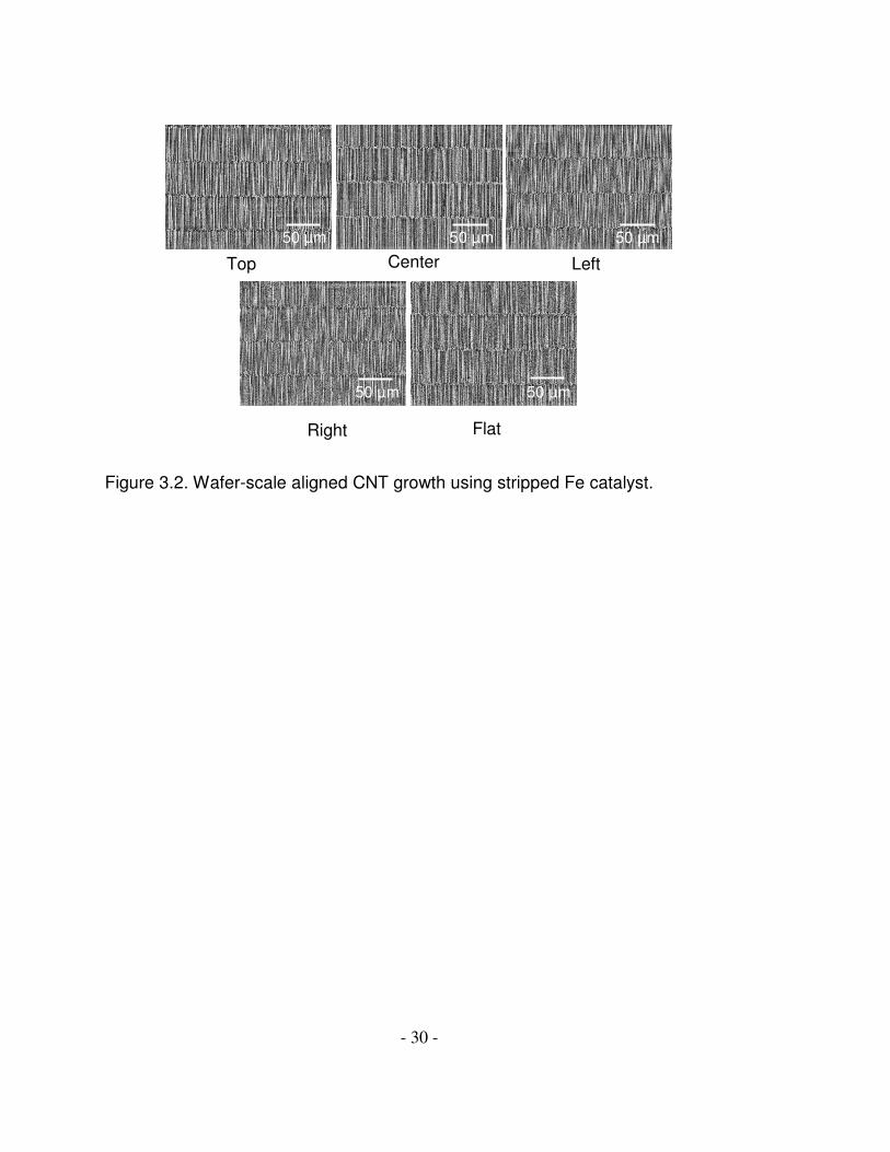
CNT alignment and density can be significantly improved with patterned catalyst
with ~99.5% of CNTs being aligned. Design principles described in [Patil 07, 08b] can
be used to fabricate VLSI CNFET circuits that function correctly in the presence of the
small fraction of misaligned CNTs. We show that full-wafer aligned CNT growth on
quartz is possible with patterned catalyst (Fig. 3.2). CNT growth was carried out using
the process illustrated in Fig. 3.1. We used 0.2 nm of evaporated Iron (Fe) catalyst in
photo-lithographically defined stripes. It is desirable to maximize the ratio of aligned
CNT area to the catalyst area so that a large fraction of devices have aligned CNTs. We
used different catalyst stripe widths (W) ranging from 0.5 µm to 10 µm and catalyst
stripe spacing (S) between 50 µm and 1200 µm (Fig. 3.3). The CNT have an average
length of ~ 400 µm and an average density of 5-10 CNTs / µm. The longest CNTs are
approximately 675 µm in length (Fig. 3.3a). The maximum catalyst spacing, for which
CNT density is uniform between stripes, is approximately equal to the CNT length (~400
µm). Experimental results show that the catalyst strip can be as narrow as 0.5 µm. It may
be possible to further reduce the width of the catalyst strip, while retaining high CNT
density between the stripes.
- 30 -
Top Center Left
Right Flat
50 µm 50 µm
50 µm 50 µm
50 µm
Figure 3.2. Wafer-scale aligned CNT growth using stripped Fe catalyst.

- 31 -
Figure 3.3. Effect of catalyst width (W) and spacing (S) on CNT density and CNT
coverage. (a) W = 10 µm, S = 1200 µm. (Length of longest CNT in image = 675
µm). (b) W = 0.5 µm, S = 50 µm. (c) W = 0.5 µm, S = 100 µm. (d) W = 1 µm, S =
50 µm. (e) W = 2 µm, S = 50 µm. (f) W = 4 µm, S = 50 µm. (g) W = 1 µm, S =
100 µm. (h) W = 2 µm, S = 100 µm. (i) W = 4 µm, S = 100 µm. (j) W = 1 µm, S =
200 µm. (k) W = 2 µm, S = 200 µm. (l) W = 4 µm, S = 200 µm.
3.2 CNT Growth Characterization
The CNTs have a mean diameter (µd) of 1.2 nm with a standard deviation (σd) of
0.3 nm (Fig. 3.4b) as measured from Atomic Force Microscopy (AFM) images (Fig.

- 32 -
3.4a). Figure 3.5a shows an optical micrograph of a quartz wafer after CNT growth. The
wafer was patterned with contacts [Ti (5 nm) / Au (40 nm)] using photolithography and
e-beam evaporation of metals. We conducted two-terminal measurements of 18 devices
with Width = 50 µm / Length = 1 µm (Fig. 3.5) in an arbitrarily selected die in each
region (top, left, center, right and flat) of the wafer. The measured current is due to the
CNTs bridging the contacts and provides a measure of the electrical uniformity of the
CNTs across the wafer. Figure 3.6 shows the mean current and the standard deviation of
these two terminal measurements at a bias of 1V. The standard deviation of CNT current
equals to ~25% of the mean current in all regions. The variation in current is due to CNT
density variation and variation in the CNT contact resistance.
0 1 2 30
5
10
15
CNT Diameter (nm)
Co
un
t µd = 1.2 nmσd = 0.3 nm
Figure 3.4 (a) AFM image of aligned CNTs on quartz. (b) CNT diameter
distribution.

- 33 -
Top
Flat
CenterLeft Right
a
10 µmContact
Contact
2 µm2 µm
Aligned CNTsb
RCNT
Contact 1 = 0V
Contact 2 = 1V
I…
c
Figure 3.5 (a) Optical micrograph of 4” ST-cut quartz wafer after aligned CNTs
growth and subsequent patterning of contacts. (b) SEM Image of aligned CNTs
bridging two contacts (c) Two terminal measurement parameters.
µ = 116 µAσ / µ = 22 %
n = 16
µ = 78 µA
σ / µ = 32 %
n = 18
µ = 114 µA
σ / µ = 25 %n=17
µ = 189µA
σ / µ = 21 %n=18
µ = 224 µA
σ / µ = 20 %n = 16
0
2
4
6
8
12
0
15
0
18
0
21
0
24
0
27
0
30
0
Current (µA)
Co
un
t
0
2
4
6
8
0 30
60
90
12
0
15
0
18
0
Current (µA)
Co
un
t
0
2
4
6
8
0 30
60
90
12
0
15
0
18
0
Current (µA)C
ou
nt
0
2
4
6
8
90
12
0
15
0
18
0
21
0
24
0
27
0
Current (µA)
Co
un
t
0
2
4
6
8
0 30
60
90
12
0
15
018
0
Current (µA)
Co
un
t
Top Center Right FlatLeft
Figure 3.6. Two terminal current distributions at 1V bias for n functional devices
(out of 18) (Width = 50 µm, Length = 1 µm) in 5 arbitrary dies (out of 197 dies on
the wafer) over 5 regions of the quartz wafer.
3.3 Wafer-scale CNT Transfer
For VLSI integration of CNFETs on silicon, aligned CNTs need to be transferred
from quartz to silicon on a wafer-scale. Transfer of aligned CNTs grown on quartz wafer-
pieces to silicon substrates using gold and polyimide was first demonstrated in [Kang 07].
Here we describe a new CNT transfer technique that can be used to transfer CNTs from
quartz to silicon on a wafer-scale. This low temperature (90oC–120
oC) transfer procedure

- 34 -
uses thermal release adhesive tape (Nitto Denko, Part Number: #3198MS) and preserves
CNT density and alignment (Fig. 3.7). Unlike aligned CNT growth which requires high
temperatures, CNT transfer is a low temperature process and enables the integration of
CNTs on already fabricated silicon CMOS wafers, dies, and flexible substrates.
.
CNTs on Quartz before Transfer
CNTs on SiO2 / Siafter Transfer
20 µm 20 µm
50 µm 50 µm
CNT
Transfer
Figure 3.7. SEM images of transferred CNTs.

- 35 -
a
c
d
4” (100 mm)
b
4” (100 mm)
4” (100 mm)
e
120oC
f
2 µm
2 µm
Figure 3.8. CNT transfer technique.
Figure 3.8 illustrates the CNT transfer technique. Aligned CNTs are grown on a
quartz wafer (Fig. 3.8a). A gold film (100 nm) is evaporated on the quartz wafer using e-
beam evaporation (Fig. 3.8b). Thermal release tape is applied to the gold film and the
tape/gold bilayer is peeled off from the quartz substrate (Fig. 3.8c). The CNTs remain
embedded in the gold layer. This tape/gold bilayer is then applied to the target wafer. The
target wafer is then heated to the release temperature of the tape (90oC or 120
oC,
depending upon the type of thermal release tape). At this temperature, the tape loses
adhesion and peels off, while the gold, along with the embedded CNTs, sticks to the
target substrate (Fig. 3.8d). Oxygen plasma descum (55W, 25 mTorr, 20 sccm O2) for 3
minutes is then used to remove organic residues from the gold surface after transfer. The
gold is then removed using gold etchant (Transcene Corp. KI/I2) which leaves the CNTs

- 36 -
on the target wafer. Figure 3.8e shows an SEM image of the transferred CNTs on a
silicon wafer. CNT density and alignment is preserved as can be seen from Fig. 3.7 and
Fig. 3.8e.
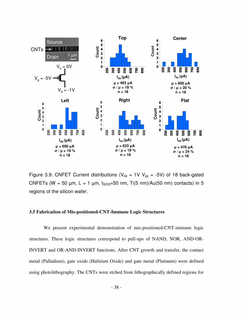
3.4 CNFET Characterization
We also fabricated back-gated CNFETs by transferring CNTs grown on quartz
wafers to silicon wafers with thermal oxide. Fabricated CNFETs had a low Ion / Ioff ratio
due to the presence of metallic CNTs. To assess the electrical uniformity of the
transferred CNTs across the wafer, we measured the Ion (Vgs = -5V, Vds = -1V)
distributions of CNFETs. For this electrical characterization, we measured 18 identically
sized (Width = 50 µm, Length = 1 µm) arbitrarily chosen CNFETs in each the five
regions (top center, left, right and flat) of the wafer (out of a total of ~100,000 CNFETs
fabricated) (Fig. 3.9).
SEM images indicate an average CNT density of approximately 4 CNTs / µm.
For the 50 µm wide CNFETs, there are, on average, 200 CNTs per CNFET. The average
CNFET on-current across the wafer is 552 µA corresponding to CNFET average current
density of 11 µA/µm. For the performance gains over CMOS projected in [Wei 09b],
CNT density must be improved to >100 CNTs/µm. One potential technique to attain high
CNT density is to perform wafer-scale CNT transfer (Fig. 3.8) multiple times from
multiple quartz wafers to the same target silicon wafer. A modification of the above CNT
transfer technique can be used to perform multiple transfer of CNTs. An additional
plasma processing (100W, 12.5 mTorr, 15 sccm Ar) step is used to partially etch the

- 37 -
transferred gold film (Fig. 3.8d) before removing the rest of the film using gold etchant
(Transcene Corp. KI/I2).
CNT transfer can also be used to create monolithically integrated CNFET three-
dimensional integrated circuits (3D IC) with CNFETs in multiple layers of the chip
interconnected through conventional vias. Such a monolithic CNFET 3D IC was
experimentally demonstrated in [Wei 09a] using the CNT transfer technique described in
this chapter.
- 38 -
µ = 463 µAσ / µ = 18 %
n = 18
µ = 600 µAσ / µ = 20 %
n = 18
µ = 476 µAσ / µ = 24 %
n = 18
µ = 600 µA
σ / µ = 19 %n = 18
µ = 623 µAσ / µ = 19 %
n = 18
Source
Drain
Vg = -5V
Vs = 0V
Vd = -1V
CNTs1 µm C
ou
nt
Ids (µA)
Top
0
1
2
3
4
5
6
250
350
45
0
55
0
65
0
750
850
0
1
2
3
4
5
6
250
350
45
0
55
0
65
0
750
850
Co
un
t
Ids (µA)
Center
0
1
2
3
4
5
6
25
0
35
0
45
0
55
0
65
0
75
0
85
00
1
2
3
4
5
6
25
0
35
0
45
0
55
0
65
0
75
0
85
0
Co
un
t
Ids (µA)
Left
0
1
2
3
4
5
6
25
0
35
0
45
0
55
0
65
0
75
0
85
0
Co
un
t
Ids (µA)
Right
0
1
2
3
4
5
6
25
0
35
0
45
0
55
0
65
0
75
0
85
0
Co
un
t
Ids (µA)
Flat
0
1
2
3
4
5
6
25
0
35
0
45
0
55
0
650
750
85
00
1
2
3
4
5
6
25
0
35
0
45
0
55
0
650
750
85
0
Figure 3.9. CNFET Current distributions (Vds = 1V Vgs = -5V) of 18 back-gated
CNFETs (W = 50 µm, L = 1 µm, tSiO2=50 nm, Ti(5 nm)/Au(50 nm) contacts) in 5
regions of the silicon wafer.
3.5 Fabrication of Mis-positioned-CNT-Immune Logic Structures
We present experimental demonstration of mis-positioned-CNT-immune logic
structures. These logic structures correspond to pull-ups of NAND, NOR, AND-OR-
INVERT and OR-AND-INVERT functions. After CNT growth and transfer, the contact
metal (Palladium), gate oxide (Hafnium Oxide) and gate metal (Platinum) were defined
using photolithography. The CNTs were etched from lithographically defined regions for

- 39 -
mis-positioned-CNT-immune logic structures (Fig. 3.10d). Metallic-CNTs were removed
using electrical breakdown [Collins 01] after fabrication of the logic structures to
improve the on-off ratio of the CNFETs. Electrical breakdown is not scalable for VLSI
and a VLSI-compatible metallic CNT removal technique will be described in Chapter 4
of this thesis. Further details of the fabrication process can be found in [Patil 08a].
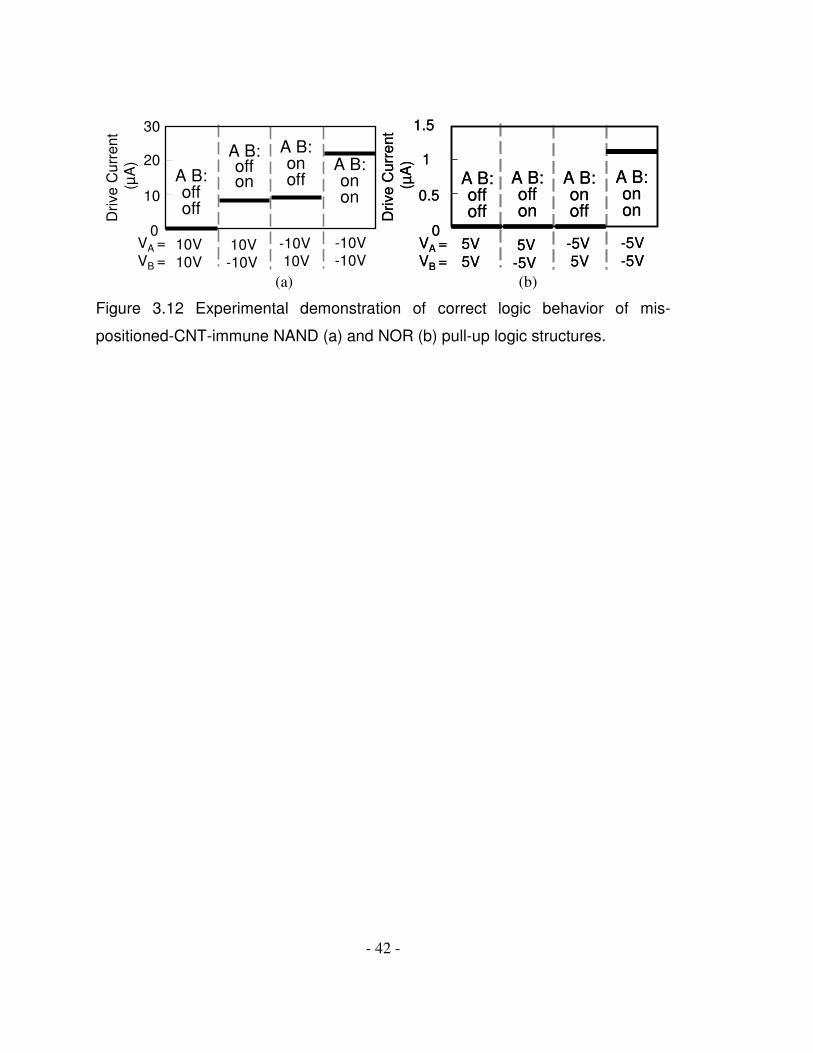
Consider the NAND pull-up (Fig. 3.11a and Fig. 3.12a). When both gates are off,
the drive current (Idrive) is very small. When both gates are on, Idrive is maximum, and
when only one of the gates is on, Idrive is approximately half-way between minimum and
maximum values. For the NOR pull-up (Fig. 3.11b and Fig. 3.12b). The drive current is
large only when both gates are on; when either of the gates is off, the drive current is very
small. The voltages applied at the inputs of the logic gates are relatively large due to
limitations associated with the electrical breakdown of metallic CNTs (see Sec. 4.1). A
new VLSI-compatible metallic CNT removal technique, described in Chapter 4 of this
thesis, overcomes these limitations.

- 40 -
Oxide & Substrate (50nm SiO2 on Si)
Source / DrainContact
50nm SiO2 10nm HfO2
Gate
CNT
Oxide & Substrate (50nm SiO2 on Si)
Source / DrainContact
50nm SiO2 10nm HfO2
Gate
CNT
BA
Vdd
Out
BA
Vdd
Out
a b
c d
Region where etching step is applied (predefined during layout design)
Contacts
CNTs
Gate
10nm HfO2
CNT
10nm HfO2
CNT
2 µm
Figure 3.10. Mis-positioned-CNT-immune CNFET circuits (a) Cross-section of
CNFET. (b) SEM of fabricated CNFET. (c) Mis-positioned-CNT-immune NAND
pull-up before etching. (d) Mis-positioned-CNT-immune NAND pull-up after
etching.

- 41 -
CNTs
A B
Vdd
IdriveOut
A B
Idrive
Vdd
Out
Gate A Gate B
Etched Region Pre-defined during layout design
A BA B BA
Vdd
BA
Out
A
B
Vdd
Idrive
Out
A
B
Idrive10 µmOut
Vdd
Gate A
Gate B
Vdd
A
Out
B
Out
Vdd
Gate A
Gate B
Out
Vdd
Gate A
Gate B
a
b
C
A B
Vdd
OutC
A B
Vdd
Out Out
Misaligned -CNT Misaligned -CNT
BA
C
Out
Misaligned -CNT Misaligned -CNT
Vdd
BA
C
BCCC
A
Vdd
Out
BCCCC
A
Vdd
Out Out
Vdd
A
C B
c
d
Out
Gate A
Gate C
Vdd
Gate B
5 µmOut
Vdd
Gate A
Gate BGate C
5 µmCNTs
10 µm
Figure 3.11. Experimental demonstration of Mis-positioned-CNT-immune logic
structures. SEM images of Logic structures corresponding to (a) NAND pull-up
(b) NOR pull-up (c) AND-OR-INVERT pull-up (d) OR-AND-INVERT pull-up.
- 42 -
30
10
20
0VA =
VB =10V10V
10V-10V
-10V10V
-10V-10V
Dri
ve
Cu
rre
nt
(µA
)
A B:off off
A B:offon
A B:on off
A B:on on
1.5
0.5
1
0VA =VB =
5V
5V 5V
-5V
-5V5V
-5V
-5V
Drive C
urr
ent
(µA
)
A B:on on
A B:offon
A B:on off
A B:off off
1.5
0.5
1
0VA =VB =
5V
5V 5V
-5V
-5V5V
-5V
-5V
Drive C
urr
ent
(µA
)
A B:on on
A B:offon
A B:on off
A B:off off
(a) (b)
Figure 3.12 Experimental demonstration of correct logic behavior of mis-
positioned-CNT-immune NAND (a) and NOR (b) pull-up logic structures.

- 43 -
Chapter 4: VMR: VLSI-Compatible Metallic CNT Removal
© [2009] IEEE. Part of this chapter has been reproduced with permission from N. Patil,
et al., “VMR: VLSI-Compatible Metallic Carbon Nanotube Removal for Imperfection-
Immune Cascaded Multi-Stage Digital Logic Circuits using Carbon Nanotube FETs”,
Proc. International Electron Devices Meeting, pp. 573-576, 2009.
A CNT can be either metallic (m-CNT) or semiconducting (s-CNT) depending on
its chirality [Saito 98]. m-CNTs have zero or near-zero bandgap and, hence, their
conductivity cannot be controlled by the gate. The existence of m-CNTs inside CNFETs
creates source-to-drain shorts. The best way to solve the m-CNT problem is to have
predominantly s-CNTs on the substrate to start with. Typical CNT synthesis techniques
yield ~33% metallic CNTs [Dai 02]. Preferential s-CNT growth techniques yields 90-
96% s-CNTs [Ding 09, Li 04]. Reduction in the percentage of m-CNTs has also been
demonstrated when CNTs are deposited onto the wafer via a self-sorting technique
[LeMieux 08]. Solution-based CNT sorting techniques yield 1-10% m-CNTs [Engel 08,
LeMieux 08]. While such improvement in percentage of m-CNTs (i.e., lower percentage
of m-CNTs) is necessary, this alone is not sufficient for VLSI CNFET circuits. For VLSI
CNFET circuits to meet leakage, noise margins, and delay variation targets, the
percentage of m-CNTs must be reduced to less than 0.01% [Zhang 08, 09]. In the absence

- 44 -
of 99.99+% s-CNT growth, the other processing option is to remove m-CNTs after CNT
growth from an ensemble of m-CNTs and s-CNTs on the substrate.
4.1 Existing m-CNT Removal Techniques
For CNFET-based VLSI circuits to achieve a target Ion/Ioff of 104, 99.99% of all
m-CNTs must be removed if the initial percentage of m-CNTs equals 33% [Zhang 08].
Existing techniques for metallic CNT removal are either not VLSI-compatible [Collins
01] or do not remove enough m-CNTs [Engel 08, LeMieux 08]. Metallic CNTs can be
removed after growth using sorting [Engel 08, LeMieux 08], selective chemical etching
[Zhang 06] or current-induced breakdown [Collins 01], which we refer to as Single-
Device electrical Breakdown (SDB). In SDB, s-CNTs are switched off using the gate so
that current only flows through m-CNTs. At high current levels, oxidation is induced by
self-heating of m-CNTs causing them to break down. This approach has the advantage of
high removal percentage of m-CNTs [Collins 01, Lin 09a]. However, a major drawback
for this technique is that it is not scalable for VLSI systems since it involves individually
contacting and breaking down m-CNTs in each CNFET. Further, SDB requires the gate
oxide of CNFETs to be thick enough to withstand high source-drain voltage applied
during breakdown (3V-10V [Pop 08]) resulting in reduced circuit performance.
Moreover, SDB does not completely remove the metallic CNTs and only creates breaks
in the metallic CNTs. The resulting metallic CNT fragments can cause shorts in CNFET
logic circuits (Fig. 4.1).

- 45 -
Output Contact
Gnd Contact
Internal Contact
A B
C D
VDS,Breakdown
m-CNT broken
Metallic CNTs (m-CNTs)
Semiconducting CNTs (s-CNTs)
Intact m-CNT fragment Wanted:
(A + B) • (C + D)
Got:
(C + D)
Gnd
Figure 4.1. Incorrect logic functionality due to m-CNT fragments left behind after
Single Device Breakdown (SDB).
4.2 VMR Technique and Experimental Results
We present a new technique called VMR (VLSI-compatible Metallic CNT
Removal) that overcomes the VLSI challenges of existing m-CNT removal techniques.
Experimental results demonstrate that VMR is compatible with VLSI processing and
produces multiple-CNT CNFETs that exhibit high Ion/Ioff of 103 to 10
5. VMR successfully
overcomes the VLSI challenges faced by SDB and is scalable to VLSI CNFET circuits.
Figure 4.2 shows VMR process steps.

- 46 -
VMR electrodes
Back-gate oxide
Silicon Substrate
CNTs
Step 1 Step 3Step 2
Top gates
InterconnectEtched regions
Figure 4.2. Optical micrographs and illustrations of VMR process steps.
Aligned CNTs are grown on single-crystal quartz wafers and then transferred to
silicon wafers with thick (100 nm) silicon dioxide as the back-gate oxide [Kang 07, Patil
08a, 09b]. A special layout called VMR structure is fabricated (Fig. 4.2, Step 1, Fig. 4.3
and Fig. 4.4a). The VMR structure consists of inter-digitated electrodes (Palladium) at
minimum metal pitch.
Next, VLSI-compatible m-CNT electrical breakdown is performed by applying
high voltage across m-CNTs all at once using the VMR structure (Fig. 4.5). Electrical
breakdown of metallic CNTs was conducted using a parameter analyzer (Agilent 4155A)
and a source meter (Keithley 2420) controlled using LabVIEW over GPIB. The silicon
back-gate turns off semiconducting CNTs (s-CNTs). After m-CNT breakdown, all VMR
structures exhibit high Ion/Ioff (Fig. 4.6).
The VMR structures are then divided into multiple individual CNFETs by etching
unwanted sections of the VMR electrodes (Fig. 4.2, Step 2 and Fig. 4.4b) by wet etching

- 47 -
of Palladium in dilute aqua regia (3:1:4 HCl:HNO3:H20) using photoresist as a mask.
Sections of the VMR electrodes that will form CNFET contacts in the final circuit are not
removed. CNTs are etched from predefined layout regions corresponding to the final
intended circuit (using mis-positioned-CNT-immune layouts [Patil 07, 08b]).
Fabrication of the final intended circuit is completed by patterning top-gates with
thin-oxide, and interconnects that span multiple metal layers (Fig. 4.2, Step 3 and Fig.
4.4c). Specifically for the experiments described in this chapter and the next,
interconnects (bilayer of 10 nm Ti and 25 nm Pt), top-gate oxide (8 - 12 nm HfO2,
Atomicity Inc.) and top-gate metal (bilayer of 2 nm Ti and 40 nm Pt) were defined using
photolithography and liftoff. Enhancement-mode CNFETs (negative threshold voltage
for p-type CNFETs) with well-behaved current-voltage characteristics are obtained after
VMR (Fig. 4.8). Enhancement-mode CNFETs are necessary for cascaded CNFET
circuits (see Chapter 5).
The VMR structure is independent of the final intended design. However, any
arbitrary final design (e.g., Fig. 4.4d) can be created by etching out parts of the VMR
structure as long as the following modification is incorporated in logic library cell
layouts: An additional contact (at minimum metal pitch) is added for series-connected
CNFETs for logic library cells (Fig. 4.7). Regions of the VMR structure to be etched out
are pre-defined during layout design and no die-specific customization is required. The
additional contacts incur < 2% area penalty and 3% delay penalty at the chip level, based
on synthesis results of large designs (OpenRISC processor, Ethernet controller
[OpenCores]). The penalties associated with the contacts are small since for advanced

- 48 -
technology nodes, the layout is already on a regular grid and the addition of contacts does
not increase the area for most of the standard logic cells. The additional contacts increase
the capacitance, resulting in a small delay penalty (3%).
Silicon Back-Gate
Back-Gate Oxide
20 µm
2 µm
AlignedCNTs
Minimum metal pitch
Width of VMR
electrodes
(c)
(b)VMR electrode thickness
Inter-digitatedVMR electrodes
AlignedCNTs
(a)
Figure 4.3. Top view (a) and cross-sectional view (b) of VMR structure consisting
of 6 inter-digitated VMR electrodes. (c) SEM Image of VMR structure (top view).

- 49 -
Metal 1
Via
Top gate
P-doped CNTs
N-doped CNTs
A
B
S S__
S S__
S__
S
S__
A
B S
S__
S__
GND
VDDVDD
GND
BA
(c) (d)
(a)(b)
Metallic CNTs (m-CNTs)
Semiconducting CNTs (s-CNTs)
InverterInverter
Complex gate
S
Source and Drain Contacts
Figure 4.4. VMR example for an arbitrary final design.
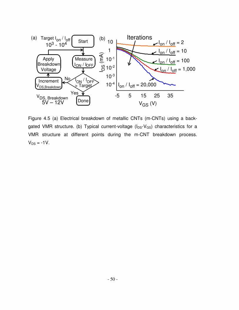
- 50 -
IncrementVDS,Breakdown
ION / IOFF
ION/ I
OFF> Target
ApplyBreakdown
Voltage
No
Yes
Done
Start
Measure 10-1
1
10
-5 5 15 25 35
Ion / Ioff = 2
Ion / Ioff = 10
Ion / Ioff = 100
Ion / Ioff = 20,000
Ion / Ioff = 1,00010-2
10-3
10-4
I DS
(mA
)VGS (V)
Iterations(a) (b)
VDS, Breakdown5V – 12V
Target Ion / Ioff
103 - 104
Figure 4.5 (a) Electrical breakdown of metallic CNTs (m-CNTs) using a back-
gated VMR structure. (b) Typical current-voltage (IDS-VGS) characteristics for a
VMR structure at different points during the m-CNT breakdown process.
VDS = -1V.

- 51 -
30
20
10
010 102 103 104 105
I on
(mA
)
Ion / Ioff
25 inter-digitated VMR electrodes21 inter-digitated VMR electrodes
7 inter-digitated VMR electrodes13 inter-digitated VMR electrodes
Before VMR
After VMR
Figure 4.6. Ion vs. Ion / Ioff for 104 VMR structures with 7, 13, 21, 25 inter-digitated
VMR electrodes. VMR electrode width = 50 µm. Average s-CNT current yield,
defined as (Ion–Ioff)After_VMR / (Ion–Ioff)Before_VMR, is 95%. Ion is measured at VGS = -
5V. Ioff is measured at VGS = 40V. High back-gate voltage is needed because of
the thick back-gate oxide (100 nm SiO2).
VMR retains the benefits of SDB while overcoming VLSI challenges faced by
SDB:
1. VMR does not require any top-gate because the back-gate is used for m-CNT
breakdown. This enables thin top-gate oxide to be fabricated for high performance
CNFETs after m-CNT breakdown. The effect of the back-gate capacitance during normal
circuit operation can be minimized by using a thick back-gate oxide since the back-gate is
not needed during normal circuit operation.
2. VMR does not require any mechanism to contact each CNFET separately.

- 52 -
3. The problem of m-CNT fragments is overcome since all internal contacts can
be accessed using the VMR structure (parts of which are etched to create the final
intended design).
BA
VDD
GND
BA
VDD
GND
Metal 1
Via
Top gate
P-doped CNTs
N-doped CNTs
Source and
Drain Contacts
VDD
GND
BA
S
VDD
GND
BA
S
a
b
Figure 4.7. Layout modifications needed for VMR. (a) NAND layout with added
contacts (marked with black circle). (b) Multiplexer layout with added contacts
(marked with black circles).

- 53 -
(a) (b)
-100
-200
-300
-400
-3 -2 -1 0
VDS (V)
VGS = -3V, -2V, -1V, 0V
IDS
(µA
)
VGS (V)
-3 -2 -1 0 1 2 3
-100
-10
-1
IDS (µA)
Figure 4.8. Typical current-voltage characteristics (a) IDS-VGS (VDS = -1V) (b) IDS-
VDS (VGS step = 1V) of a multiple-CNT CNFET (Width = 50 µm, Length = 1 µm,
Number of CNTs = ~100) after VMR and fabrication of top-gate oxide (12 nm
HfO2) and top-gate metal: bilayer of Titanium (2 nm) and Platinum (25 nm). The
threshold voltage of the CNFETs is negative (enhancement-mode p-type
CNFETs) enabling CNFET logic gates that can be cascaded.
4.3 VMR Scalability
Figure 4.9 shows the resistor network representing a VMR structure with multiple
metallic and semiconducting CNTs. We can simulate the metallic CNT breakdown
procedure for the VMR electrodes using this resistor network. Initially, due to voltage
drops across the electrodes (voltage profiles across the electrodes are shown in Fig. 4.10a
and Fig. 4.10b), not all the m-CNTs will be above the threshold voltage for m-CNT
breakdown (VDS, Breakdown) [Pop 08]. However, some metallic CNTs, which are initially
above the breakdown threshold, are removed. This reduces the current through the
electrodes, thereby reducing the voltage drops. Eventually, in a carefully designed VMR
structure, all the m-CNTs are removed (Fig. 4.10a). On the other hand, for wider VMR
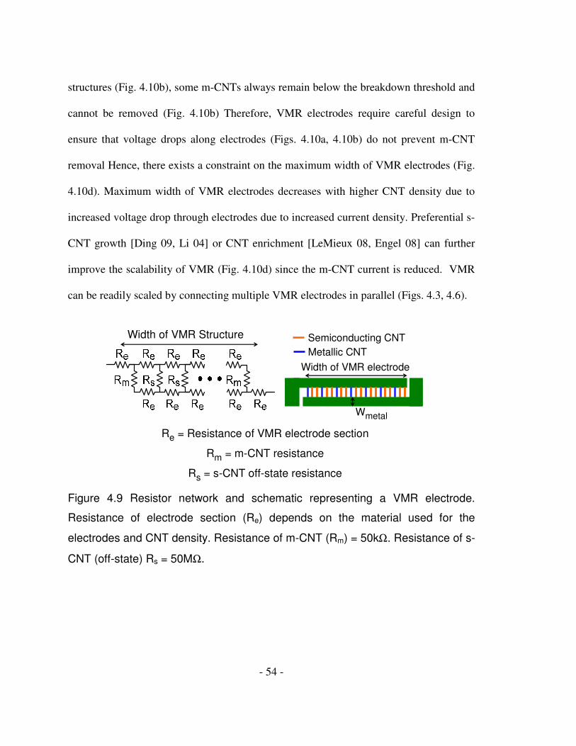
- 54 -
structures (Fig. 4.10b), some m-CNTs always remain below the breakdown threshold and
cannot be removed (Fig. 4.10b) Therefore, VMR electrodes require careful design to
ensure that voltage drops along electrodes (Figs. 4.10a, 4.10b) do not prevent m-CNT
removal Hence, there exists a constraint on the maximum width of VMR electrodes (Fig.
4.10d). Maximum width of VMR electrodes decreases with higher CNT density due to
increased voltage drop through electrodes due to increased current density. Preferential s-
CNT growth [Ding 09, Li 04] or CNT enrichment [LeMieux 08, Engel 08] can further
improve the scalability of VMR (Fig. 4.10d) since the m-CNT current is reduced. VMR
can be readily scaled by connecting multiple VMR electrodes in parallel (Figs. 4.3, 4.6).
Width of VMR Structure
Re = Resistance of VMR electrode section
Rm = m-CNT resistance
Rs = s-CNT off-state resistance
Metallic CNT
Semiconducting CNT
Width of VMR electrode
Wmetal
Figure 4.9 Resistor network and schematic representing a VMR electrode.
Resistance of electrode section (Re) depends on the material used for the
electrodes and CNT density. Resistance of m-CNT (Rm) = 50kΩ. Resistance of s-
CNT (off-state) Rs = 50MΩ.

- 55 -
(b)(a)
0 20 40
5
10
CNT position (µm)
Vo
lta
ge
(V
) Time
VDS,Breakdown
All m-CNTs removed Not all m-CNTs removed
0 20 40 60
5
10
CNT position (µm)
Vo
lta
ge (
V) VDS,Breakdown
Time
Figure 4.10. Voltage profile simulation of a VMR electrode (Palladium) with 10V
applied at the two ends. Width of metal (Wmetal) = 100 nm (Fig. 4.9), Thickness of
palladium VMR electrodes = 100 nm. CNT density = 10 CNTs/µm. VDS,Breakdown of
m-CNTs = 5V for CNT length = 1 µm [Pop 08] (a) Width of VMR electrode = 62
µm. (b) Width of VMR electrode = 55 µm.
CNT density (CNTs/ µm)
Ma
x W
idth
(µ
m) m-CNTs = 1%
m-CNTs = 33%
1
10
100
1000
1 10 100
Figure 4.11. Maximum width of VMR electrodes.

- 56 -
As shown in Fig. 4.11, the maximum width of a VMR structure is limited by the
voltage drop across the electrodes. As a result, the pads with minimum dimension of
25 µm on each side can result in unacceptable area overheads (up to 200%) for VMR
(Fig. 4.12). [Wei 10] describes an improved metallic CNT removal technique based on
VMR with worst-case overhead of 1% (Fig. 4.12).
An array of structures, each consisting of inter-digitated Palladium (Pd) electrodes
(width constraint of each structure is imposed by m-CNT breakdown discussed in Fig.
4.11) are created at regular pitch. Unlike the version of VMR described in Sec. 4.2, each
structure belongs to one of two groups such that two spatially neighboring structures
belong to different groups (this idea can be extended to multiple groups as well). Further
details of this new technique can be found in [Wei 10].
0 10 20 30
0
50
100
150
200
Improved VMR (Sec. 4.4)
(Worst-case overhead = 1%)
VMR (Sec. 4.2)
100 CNTs/µm
VMR (Sec. 4.2)
250 CNTs/µm
% metallic CNTs
% A
rea
Ove
rhe
ad
Figure 4.12. Area cost analysis for different metallic carbon nanotube removal
techniques. Compared with VMR, improved VMR reduces the worst-case area
overhead from 200+% down to 1% at the 22 nm technology node.

- 57 -
The low area overhead of this new approach is made possible because of the
following characteristics of this technique: 1. the pad regions for the structures belonging
to one group are overlapped with the structures belonging to other group(s); 2. the choice
of metals for the electrodes vs. the pads enables such overlap and selective removal of the
pads after m-CNT electrical breakdown. In summary, this improved VMR technique
[Wei 10] achieves high Ion/Ioff of up to 106 and, at the same time, is readily scalable to
full-wafer-level with < 1% area cost.

- 58 -
Chapter 5: VLSI-Compatible Combinational and Sequential CNFET
Circuits
© [2009] IEEE. Part of this chapter has been reproduced with permission from N.
Patil, et al., “VMR: VLSI-Compatible Metallic Carbon Nanotube Removal for
Imperfection-Immune Cascaded Multi-Stage Digital Logic Circuits using Carbon
Nanotube FETs”, Proc. International Electron Devices Meeting, pp. 573-576, 2009.
We present experimental demonstrations of VLSI-compatible imperfection-
immune cascaded multi-stage logic circuits using VMR [Patil 09c], together with mis-
positioned-CNT-immune layouts [Patil 07, 08b] and wafer-scale aligned CNT growth
and transfer [Patil 08a, 09]. Previous CNFET circuit demonstrations [Cao 08, Chen 06,
Javey 03a, 03b, 05], while important, either use percolation-transport-based CNFETs, or
cannot be scaled-up for digital VLSI systems. VMR enables first experimental
demonstration of complex cascaded CNFET logic circuits. Such logic circuits are
immune to both mis-positioned and metallic CNTs.
5.1 CNFET Circuit Elements
Using the process flow detailed in Sec. 4.2, we fabricated CNFET circuit
elements (Fig. 5.1). High Ion/Ioff of 103-10
5 is achieved for various circuit elements, e.g.,
NAND, multiplexer in Fig. 5.1, fabricated using VMR. Enhancement-mode CNFETs

- 59 -
(negative threshold voltage for p-type CNFETs) with well-behaved current-voltage
characteristics are obtained after VMR (Fig. 4.8). Enhancement-mode CNFETs are
crucial in enabling CNFET circuits that can be cascaded, i.e. the output of one CNFET
logic gate can be used to drive the input to another CNFET logic gate for complex logic
circuits.
Multiplexer pull-up
NAND pull-up
Pull-down CNFET
60
100
140
1 101 102 103 104 105 106
NAND Pull-ups
20
I on
(µA
)
Multiplexer pull-ups
Pull-down CNFETs
No VMR
With VMR
Ion / Ioff
(a) (b)
Figure 5.1 (a) Circuit elements used in final CNFET circuits– Multiplexer pull-up,
NAND pull-up and pull-down CNFET. (b) Scatter plot of Ion vs. Ion/Ioff for the circuit
elements fabricated with and without VMR. All CNFETs have width = 50 µm and
length = 1 µm. Ion for circuit elements without VMR does not include m-CNT
current (Ioff). Total number of circuit elements measured = 81. All CNFET circuit
elements fabricated using VMR show high Ion/Ioff (103–105). Ion decreases after
VMR because some s-CNTs are removed during VMR (see Fig. 4.5).
- 60 -
5.2 CNFET Combinational Circuits
We can fabricate CNFET digital logic circuits using p-type CNFETs using
PMOS-only logic [McCluskey 86]. We used a p-type CNFET as a pull-down for the
CNFET circuits. Figure 9 shows an integrated CNFET inverter and NAND that can be
cascaded, i.e. the voltage transfer curves of the logic gates transition between 0 and Vdd.
Voltage swing is reduced due to the use of only p-type CNFETs similar to all-PMOS
logic [McCluskey 86]. Integration of CNT doping to fabricate n-type CNFETs can
improve the voltage swing.
Further, we present experimental demonstration of multi-stage imperfection-
immune multiple-CNT CNFET circuits fabricated in a VLSI-compatible manner. Figure
5.3 shows a CNFET inverter chain. Figure 5.4 shows a multi-stage CNFET circuit
implementing a half-adder sum generator function. All biases for the pull-down CNFETs
in the circuit are connected together similar to all-PMOS logic circuits [McCluskey 86].
Scalable CNFET logic circuits using PMOS-only logic are possible since a single bias
voltage is used for all CNFET logic gates. These cascaded CNFET circuits, fabricated
using VMR and wafer-scale processing techniques [Patil 08a, 09b], satisfy requirements
of digital logic (gain and cascadability) [McCluskey 86] in a VLSI-compatible manner.

- 61 -
IN
VDD = 2V
BIAS
=3V
GND
OUT
InverterVoltage Transfer Curve
Correct threshold voltage for
cascadability
GND
VDD = 3V
BIAS = 4V
AOUT
B
0
1
2
3
VO
UT
(V)
A: 0VB: 0V
A: 0VB: 3V
A: 3VB: 0V
A: 3VB: 3V
0 1 2V
IN(V)
0
1
2
0 1 2
VO
UT
(V)
(a)
⋅NAND: A B
10 µm
1 µm
10 µm
1 µm
(b)
CNTs
Figure 5.2. Single-stage CNFET logic gates using VMR and all-PMOS logic with
pull-down CNFETs. (a) CNFET inverter. (b) CNFET NAND.
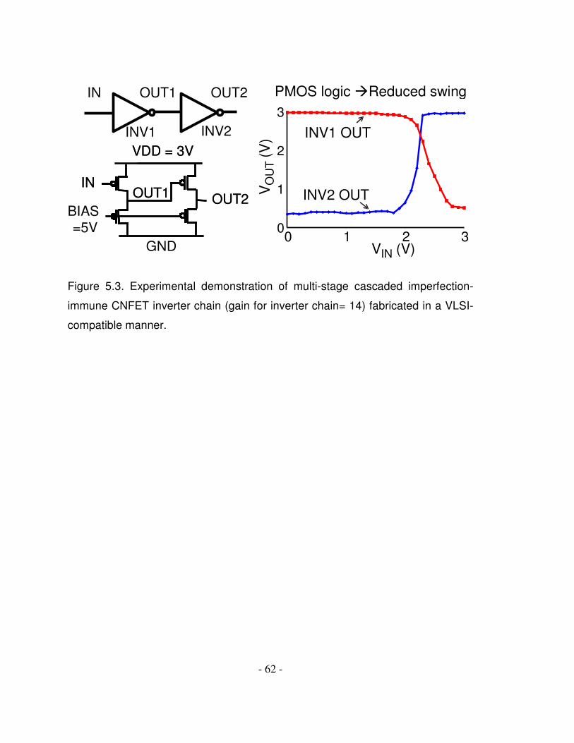
- 62 -
IN
VDD = 3V
BIAS =5V
OUT1 OUT2
INV1
IN
VDD = 3V
OUT1
GND
OUT2
INV2
IN OUT1 OUT2 PMOS logic Reduced swing
0
1
2
3
0 1 2 3VIN (V)
INV2 OUTVO
UT
(V) INV1 OUT
Figure 5.3. Experimental demonstration of multi-stage cascaded imperfection-
immune CNFET inverter chain (gain for inverter chain= 14) fabricated in a VLSI-
compatible manner.

- 63 -
0 1 2 30
1
2
3
VA (V)
VO
UT (
V)
-15
-10
-5
0
VB = 0 V
Ga
in
0 1 2 3
0
1
2
3
VO
UT (
V)
VA (V)
0
20
40
Ga
in
VB = 3 V
A B
BIAS
VDD
GND
OUT
c
b
Aligned CNTsa
111
001
010
100
FBA
111
001
010
100
FBA
Figure 5.4 (a) Scanning electron micrograph (SEM) of CNFET half-adder sum
generator implementing the equivalent of an XNOR function (left panel). Scale
bar represents 20 µm. SEM of aligned CNTs in XNOR before top-gate metal
deposition (right panel). Scale bar represents 2 µm. (b) Circuit diagram and truth
table for a half-adder sum generator. (c) Voltage transfer curves and gain for
CNFET half-adder sum generator. VBias = 4V. VDD = 3V.
5.3 CNFET Sequential Circuits
Figure 5.5 shows the first experimental demonstration of a CNFET sequential
integrated circuit (D-Latch) fabricated using VMR and PMOS-only logic. Sequential
elements such as D-Latches are essential components of digital VLSI systems. All state
transitions (Fig. 5.5c) for the CNFET D-latch were verified to be correct confirming that
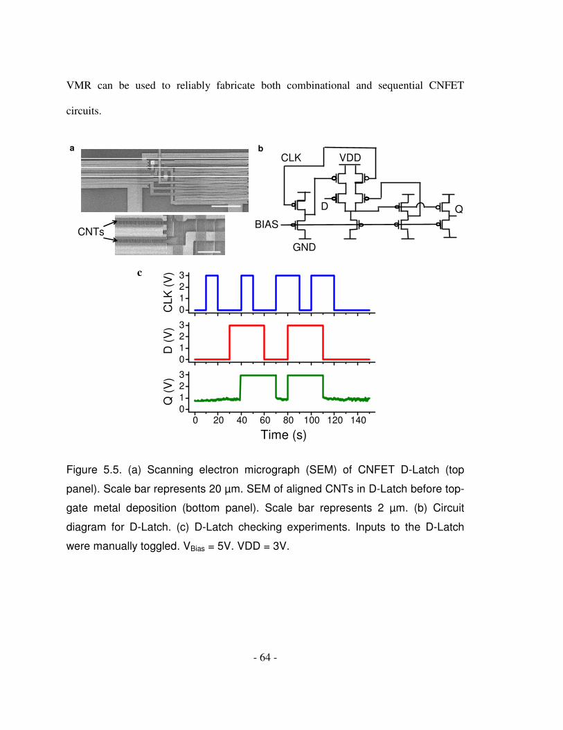
- 64 -
VMR can be used to reliably fabricate both combinational and sequential CNFET
circuits.
CLK
BIAS
VDD
GND
QD
a b
c
CNTs
0
1
23
Q (
V)
0
1
23
CL
K (
V)
0 20 40 60 80 100 120 140
0
1
23
D (
V)
Time (s)
Figure 5.5. (a) Scanning electron micrograph (SEM) of CNFET D-Latch (top
panel). Scale bar represents 20 µm. SEM of aligned CNTs in D-Latch before top-
gate metal deposition (bottom panel). Scale bar represents 2 µm. (b) Circuit
diagram for D-Latch. (c) D-Latch checking experiments. Inputs to the D-Latch
were manually toggled. VBias = 5V. VDD = 3V.
c
- 65 -
Chapter 6: Concluding Remarks
CNFET technology is a promising extension to silicon CMOS technology.
CNFET-based circuits can provide more than an order of improvement in energy-delay
product compared to silicon CMOS circuits [Deng 07a, Patil 09a, Wei 09b]. Mis-
positioned and metallic CNTs are major barriers for CNFET technology. We have
presented imperfection-immune design techniques such as mis-positioned-CNT-immune
design and VLSI-Compatible Metallic CNT Removal (VMR) to overcome the challenges
of mis-positioned and metallic CNTs.
Table 6.1 presents the current status of CNFET technology and provides a
summary of challenges and solutions.
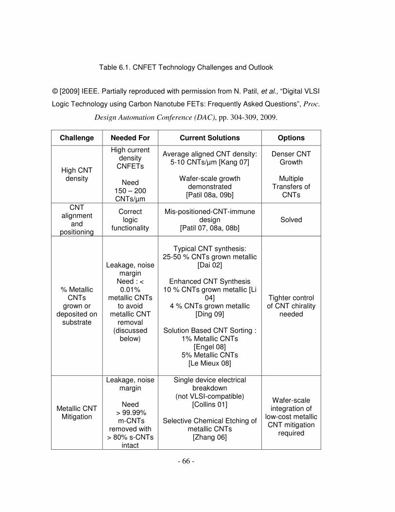
- 66 -
Table 6.1. CNFET Technology Challenges and Outlook
© [2009] IEEE. Partially reproduced with permission from N. Patil, et al., “Digital VLSI
Logic Technology using Carbon Nanotube FETs: Frequently Asked Questions”, Proc.
Design Automation Conference (DAC), pp. 304-309, 2009.
Challenge Needed For Current Solutions Options
High CNT density
High current density
CNFETs
Need 150 – 200 CNTs/µm
Average aligned CNT density: 5-10 CNTs/µm [Kang 07]
Wafer-scale growth
demonstrated [Patil 08a, 09b]
Denser CNT Growth
Multiple
Transfers of CNTs
CNT alignment
and positioning
Correct logic
functionality
Mis-positioned-CNT-immune design
[Patil 07, 08a, 08b] Solved
% Metallic CNTs
grown or deposited on
substrate
Leakage, noise margin
Need : < 0.01%
metallic CNTs to avoid
metallic CNT removal
(discussed below)
Typical CNT synthesis:
25-50 % CNTs grown metallic [Dai 02]
Enhanced CNT Synthesis
10 % CNTs grown metallic [Li 04]
4 % CNTs grown metallic [Ding 09]
Solution Based CNT Sorting :
1% Metallic CNTs [Engel 08]
5% Metallic CNTs [Le Mieux 08]
Tighter control of CNT chirality
needed
Metallic CNT Mitigation
Leakage, noise margin
Need
> 99.99% m-CNTs
removed with > 80% s-CNTs
intact
Single device electrical breakdown
(not VLSI-compatible) [Collins 01]
Selective Chemical Etching of
metallic CNTs [Zhang 06]
Wafer-scale integration of
low-cost metallic CNT mitigation
required
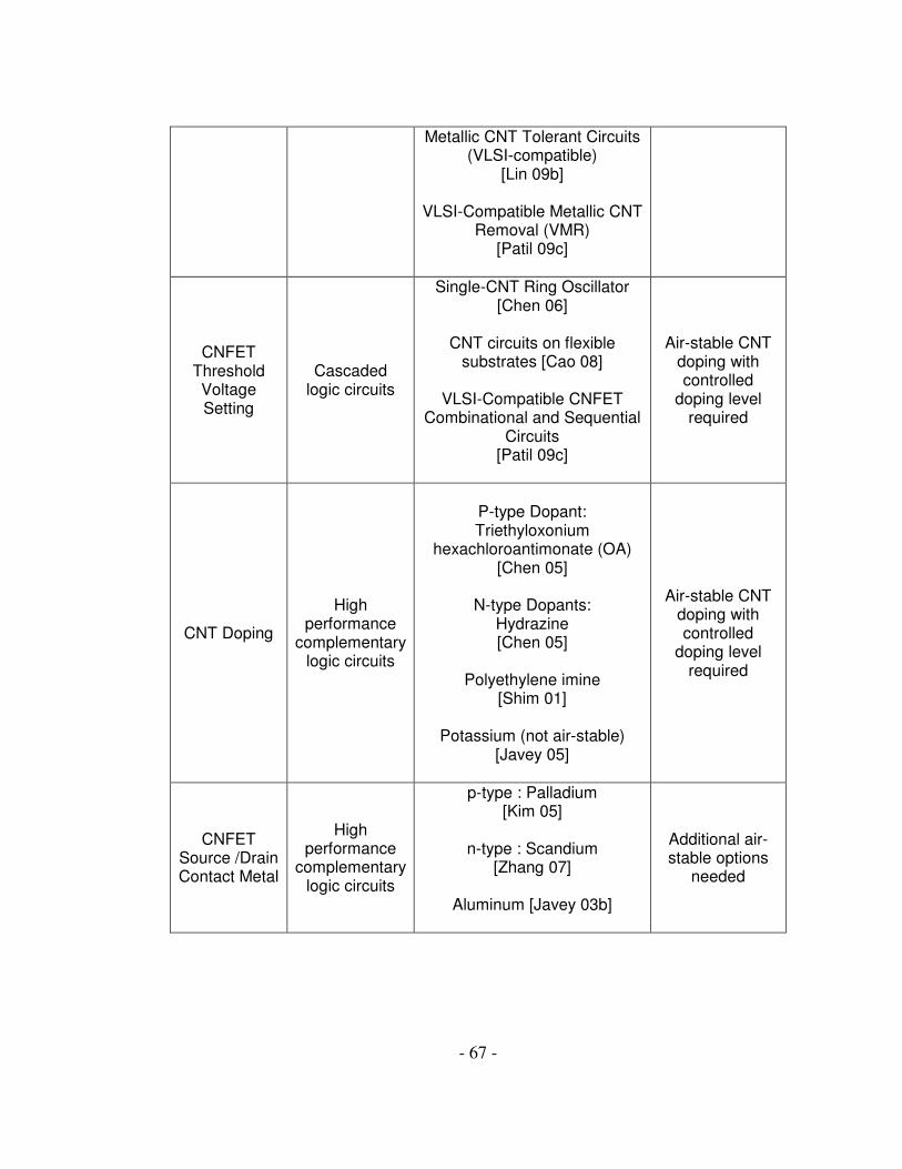
- 67 -
Metallic CNT Tolerant Circuits (VLSI-compatible)
[Lin 09b]
VLSI-Compatible Metallic CNT Removal (VMR)
[Patil 09c]
CNFET Threshold Voltage Setting
Cascaded logic circuits
Single-CNT Ring Oscillator [Chen 06]
CNT circuits on flexible
substrates [Cao 08]
VLSI-Compatible CNFET Combinational and Sequential
Circuits [Patil 09c]
Air-stable CNT doping with controlled
doping level required
CNT Doping
High performance
complementary logic circuits
P-type Dopant: Triethyloxonium
hexachloroantimonate (OA) [Chen 05]
N-type Dopants:
Hydrazine [Chen 05]
Polyethylene imine
[Shim 01]
Potassium (not air-stable) [Javey 05]
Air-stable CNT doping with controlled
doping level required
CNFET Source /Drain Contact Metal
High performance
complementary logic circuits
p-type : Palladium [Kim 05]
n-type : Scandium
[Zhang 07]
Aluminum [Javey 03b]
Additional air-stable options
needed

- 68 -
Mis-positioned-CNT-immune design, VLSI-Compatible metallic CNT removal
(VMR) can successfully overcome challenges posed by mis-positioned and metallic
CNTs. Using these imperfection-immune design and processing techniques, coupled with
wafer-scale CNT growth and transfer, we have experimentally demonstrated, for the first
time, CNFET computational and storage elements that constitute the fundamental
building blocks for digital computing.
Two significant outstanding challenges include high CNT density and CNT
doping. High CNT density (> 100 CNTs/µm) is needed for CNFET performance to be
competitive with silicon CMOS [Wei 09b]. Chemical doping of CNTs to achieve
integration of n-type and p-type CNFETs on the same substrate is also an important area
of further research in order to achieve VLSI-compatible complementary CNFET circuits.

- 69 -
Appendix: Fabrication Details
A.1 Carbon Nanotube Growth
Aligned CNT growth was carried out using ST-cut quartz wafers (Hoffman Materials,
Inc, Carlisle, PA). The quartz wafers were first annealed were annealed in oxygen for 8
hrs at 900ºC in a six-inch three-zone oxidation furnace according to the following
temperature schedule. The furnace was initially cooled down to 400 ºC (below the phase
transformation temperature of the quartz [Byers 74, Cooper 75]).
Table A.1. Annealing Schedule for Quartz Wafers
Temperature Set point Time Gas (flow rate)
400ºC 20 minutes ramp-up N2 (5L/min)
550 ºC 35 minutes ramp-up N2 (5L/min)
575 ºC 20 minutes ramp-up O2 (2.5 L/min)
(Dry oxidation condition)
600 ºC 15 minutes ramp-up O2 (2.5 L/min)
(Dry oxidation condition)
650 ºC 25 minutes ramp-up O2 (2.5 L/min)
(Dry oxidation condition)
700 ºC 25 minutes ramp-up O2 (2.5 L/min)
(Dry oxidation condition)
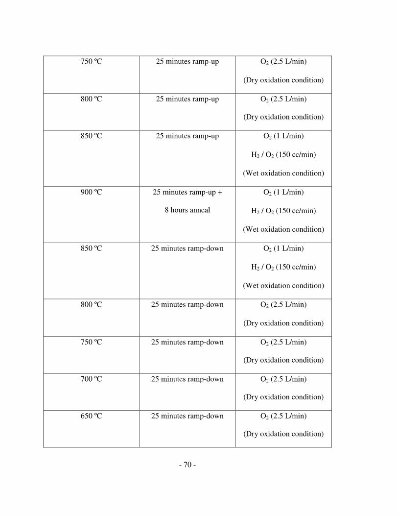
- 70 -
750 ºC 25 minutes ramp-up O2 (2.5 L/min)
(Dry oxidation condition)
800 ºC 25 minutes ramp-up O2 (2.5 L/min)
(Dry oxidation condition)
850 ºC 25 minutes ramp-up O2 (1 L/min)
H2 / O2 (150 cc/min)
(Wet oxidation condition)
900 ºC 25 minutes ramp-up +
8 hours anneal
O2 (1 L/min)
H2 / O2 (150 cc/min)
(Wet oxidation condition)
850 ºC 25 minutes ramp-down O2 (1 L/min)
H2 / O2 (150 cc/min)
(Wet oxidation condition)
800 ºC 25 minutes ramp-down O2 (2.5 L/min)
(Dry oxidation condition)
750 ºC 25 minutes ramp-down O2 (2.5 L/min)
(Dry oxidation condition)
700 ºC 25 minutes ramp-down O2 (2.5 L/min)
(Dry oxidation condition)
650 ºC 25 minutes ramp-down O2 (2.5 L/min)
(Dry oxidation condition)

- 71 -
600 ºC 25 minutes ramp-down O2 (2.5 L/min)
(Dry oxidation condition)
575 ºC 15 minutes ramp-down O2 (2.5 L/min)
(Dry oxidation condition)
550 ºC 20 minutes ramp-down O2 (2.5 L/min)
(Dry oxidation condition)
400 ºC 60 minutes ramp-down N2 (5L/min)
After the wafers were annealed, photolithographic stripes were defined on the wafers.
First a layer of LOL-2000 (Microchem) was spun on the annealed quartz wafer (3000
rpm, 60 seconds). Photoresist exhibits poor adhesion to quartz and needs an adhesion
promoter (e.g. HMDS – hexamethyldisilazane). With LOL-2000, no adhesion promoter is
needed. After coating the wafer with LOL-2000, the wafer is then baked at 200 ºC for 20
minutes. The temperature and duration of the LOL-2000 baking determines the rate of
dissolution of LOL-2000 in developer, which in turn determines the amount of undercut.
For the catalyst stripes, the spacing between the patterns was rather large (>100 µm),
hence the amount of undercut in the LOL-2000 did not cause problems in lithography.
However, for the fabrication of the CNFETs, the spacing between patterns was 1 µm or
less. In this case, as will be discussed in Sec. A.3, the LOL-2000 was baked at a higher
temperature for a longer duration so that the rate of undercut could be controlled.

- 72 -
Next, g-line photoresist (SPR 3612, Microchem) is spun on the wafer (5500 rpm, 30
seconds). After exposure (150 mJ/cm2), the wafers were developed in Microposit MF-
26A developer for a total develop time of 60s.
After patterning of lithographic stripes, a thin film of Fe was evaporated using e-beam
evaporation. The thickness of the film was monitored using a Quartz Crystal thickness
monitor. The deposition pressure was 10-6
Torr. The rate of deposition was 0.03 nm/sec
with a total nominal thickness of 0.24 nm. We found that thickness of the Fe film could
be between 0.1 nm and 0.32 nm.
Liftoff was used to remove the Fe from all regions other than the catalyst stripe.
Acetone was used to remove the photoresist followed by either Remover-PG
(Microchem) or Microposit MF-26A ((Microchem) to remove the LOL-2000.
For the growth a three-zone CVD furnace was used. The temperature uniformity of the
furnace at a pressure of ~500 mTorr was verified to be < 1ºC across the eight-inch center
zone of the furnace. This enables two wafers of CNTs to be grown simultaneously. A
longer furnace might enable more quartz wafers to be grown in parallel. The low pressure
during the critical phase transformation of the quartz (Sec 3.1) also improves the thermal
uniformity of the furnace.
With the furnace door slightly open and a flow (100 sccm) of O2 (20%) and Argon
(80%), wafers were first heated to 550 ºC. The ramp time for this step was 30 minutes.
The temperature was kept constant at 550 ºC for 10 minutes. After this step, the
temperature set point was decreased to 540 ºC. After the temperature stabilized at 540ºC,
the furnace door was closed and the furnace was pumped down to its base pressure of

- 73 -
~30 mTorr. The temperature set point was lowered before pumping the furnace because
the pumping step causes the temperature of the furnace to spike by ~10 ºC. Hence to
prevent the temperature of the furnace overshooting past the phase transformation
temperature of the quartz (573 ºC), the temperature was initially lowered before pumping
out the furnace. Next, a flow of 100 sccm of a mixture of O2 (20%) and Argon (80%) was
started. The pressure during this step was ~500 mTorr. At this low pressure, the furnace
was heated to ~620ºC in about 15 minutes. At this point, the flow of O2 (20%) and Argon
(80%) was halted and the furnace was pumped to its base pressure of ~30 mTorr. Then, a
flow of 120 sccm of H2 was started and the pressure set point was fixed to 120 Torr (the
furnace was equipped with a gate valve that could be throttled to adjust the pressure). The
temperature set point was fixed to 865 ºC (the growth temperature can be between 800 ºC
and 900 ºC). After ~8 minutes the pressure stabilized to 120 Torr (at a temperature of
~720 ºC). The total ramp time to the growth temperature was ~20 minutes. After the
temperature ramp, the furnace temperature was held at the growth temperature of 865 ºC
for 10 minutes before commencing CNT growth. Growth was conducted by co-flowing
CH4 (1100 sccm) and H2 (120 sccm) at 315 Torr for 30 minutes. The pressure set point
during CNT growth was 315 Torr (pressure can be between 300 – 350 Torr). After CNT
growth, the flow of CH4 was turned off, while the flow of H2 flow was continued. The
pressure set point was 120 Torr and the temperature of the furnace was lowered, while
keeping the two side zones of the furnace functional so that the thermal uniformity across
the quartz wafer was maintained. Once the temperature of the furnace had cooled to
300 ºC, the flow of H2 was stopped, and the furnace was pumped to its base pressure of

- 74 -
~30 mTorr. The pump isolation valve was closed and the furnace was vented to
atmosphere by flowing Ar (1000 sccm) for 8 minutes.
A.2 Carbon Nanotube Transfer
Quartz wafers with grown CNTs were coated with 100 nm Au deposited using e-beam
evaporation. The thickness of Au can be between 100 nm and 200 nm. Thermal release
adhesive tape (Nitto Denko, Inc., Part Number: 3198MS) was applied to the quartz wafer
with Au. The Au and tape bilayer was removed from the quartz wafer and then applied to
a silicon wafer. Heating to ~130ºC caused the tape to detach, leaving the gold, along with
the CNTs, on the silicon wafer. This particular type of tape had a release temperature of
120ºC. Other types of thermal release tapes are available, which release at different
temperatures. After the thermal release tape was removed, the surface of the Au (with the
CNTs under the gold), was cleaned with O2 plasma (55W, 25 mTorr, 20 sccm O2, 2
minutes) and Ar plasma (100W, 12.5 mTorr, 15 sccm Ar, 3 minutes). The Argon etching
process etched ~30 nm of gold film. The CNTs were protected from the plasma by the
remaining gold film (~70 nm). The remaining gold film was wet etched using a solution
of 17% NaI and 2% I2 in water (Transcene Corp.), leaving the CNTs on the target
substrate.

- 75 -
A.3 CNFET Circuit Fabrication
Aligned CNTs grown in quartz wafers were transferred onto silicon wafers with
115 nm thermally grown oxide. Next, inter-digitated VMR (see Chapter 4, 5) electrodes
were defined using photolithography and liftoff. Both the width of the electrodes and the
spacing between the electrodes was 1 µm. The electrodes were defined a bi-layer lift-off
process. First a layer of LOL-2000 (Microchem) was spun on the annealed quartz wafer
(3000 rpm, 60 seconds). Photoresist exhibits poor adhesion to silicon dioxide and needs
an adhesion promoter (e.g. HMDS – hexamethyldisilazane). With LOL-2000, no
adhesion promoter is needed. After coating the wafer with LOL-2000, the wafer is then
baked at ~250C for 30 minutes. The temperature and duration of the LOL-2000 baking
determines the rate of dissolution of LOL-2000 in developer, which in turn determines
the amount of undercut. Next, g-line photoresist (SPR 3612, Microchem) is spun on the
wafer (5500 rpm, 30 seconds). After exposure (55 mJ/cm2), the wafers were developed in
Microposit MF-26A (Microchem) developer for a total develop time of 50s. The bake
time, bake temperature, and the develop time together determine the smallest resolvable
feature using a bi-layer liftoff process. The metal used for the VMR electrodes was either
only palladium (50 nm thick) or a bi-layer of titanium (1.5 nm thick) and palladium (50
nm thick), deposited using e-beam evaporation at a pressure of ~5 x 10⁻⁷
Torr. The
presence of titanium improves the adhesion of palladium to the oxide surface. We also
observed that palladium-only electrodes tend to delaminate, if the wafer is immersed in
developer (MF-26A) for > 1 minute. This problem can be resolved by using a thin
titanium adhesion layer for the palladium electrodes.

- 76 -
CNTs outside the VMR electrode regions were removed using a low intensity O2
plasma (30W, 150 mTorr, 20 sccm O2, 90s) using photoresist as a mask. For this step, no
LOL-2000 was used (hence, an adhesion promoter (HMDS) was applied in the gas phase
to improve the adhesion of the photoresist). Electrical breakdown of metallic CNTs was
conducted using a parameter analyzer (Agilent 4155A) and a source meter (Keithley
2420) controlled using LabVIEW over GPIB.
After electrical breakdown of metallic CNTs, unneeded sections of the VMR
electrodes were removed using wet etching of Pd in dilute aqua regia (3:1:4
HCl:HNO3:H20, ~60s) and using photoresist as a mask. The etching was carried out ~5
minutes after the aqua regia solution was prepared. The titanium adhesion layer, if used
was then removed in 2% HF (45s). For these steps, no LOL-2000 was used (hence, an
adhesion promoter (HMDS) was applied in the gas phase to improve the adhesion of the
photoresist). Before wet etching the unneeded sections of the VMR electrodes, the
photoresist surface was made hydrophilic by a brief exposure to a low intensity O2
plasma (30W, 150 mTorr, 20 sccm O2, 180s).
Metal interconnects were defined using photolithography of a bi-layer of 10 nm
Ti and 25 nm Pt deposited using e-beam evaporation (deposition pressure = ~5 x 10⁻⁷
Torr). Next, top-gate oxide (8 nm hafnium oxide (HfO2), deposited by Atomic Layer
Deposition (ALD), Atomicity Inc, Redwood City, CA), and top-gate metal (bilayer of 2
nm Ti and 40 nm Pt using e-beam evaporation) were subsequently defined using
photolithography and liftoff. Since the gate oxide regions were defined liftoff, the ALD
deposition temperature was kept at 110ºC to avoid photoresist reflow at higher
- 77 -
temperatures. ALD aluminum oxide (Al2O3) can also be used as gate-oxide. However,
aluminum oxide dissolves in developer (MF-26A, etch-rate = 0.1-0.3 nm/s depending
upon the quality of the film). Hence, the gate stack should not be exposed to developer
for extended periods to avoid undercutting the oxide under the gate metal. Connections
between the metal interconnect and the gate metal (so that the output of one CNFET logic
gate can be connected to the input of the next CNFET logic gate) were done through
photolithography and liftoff of 26 nm Cr and 200 nm Au deposited using an RF
sputtering system.
All CNFET circuit measurements were performed in room ambient using a
semiconductor parameter analyzer (Agilent 4155A).

- 78 -
Publications
1. H. Wei, N. Patil, J. Zhang, A. Lin, H.-S. P. Wong and S. Mitra, “Efficient Metallic
Carbon Nanotube Removal Readily Scalable to Wafer-Level VLSI CNFET Circuits,”
Proc. Symposium on VLSI Technology, paper 22.4, 2010.
2. J. Zhang, N. Patil, A. Lin, H.-S.P. Wong and S. Mitra, “Carbon Nanotube Circuits:
Living with Imperfections and Variations,” Proc. Design Automation and Test in
Europe (DATE), pp. 1159-1164, 2010 (Invited).
3. J. Zhang, S. Bobba, N. Patil, A. Lin, H.-S.P. Wong, G. De Micheli and S. Mitra,
“Carbon Nanotube Correlation: Promising Opportunity for CNFET Circuit Yield
Enhancement,” Proc. Design Automation Conference (DAC), paper 51.3, 2010.
4. N. Patil, A. Lin, J. Zhang, H. Wei, K. Anderson, H.-S. P. Wong and S. Mitra, “VMR:
VLSI-Compatible Metallic Carbon Nanotube Removal for Imperfection-Immune
Cascaded Multi-Stage Digital Logic Circuits using Carbon Nanotube FETs”, Proc.
International Electron Devices Meeting (IEDM), pp. 573-576, 2009.
5. N. Patil, A. Lin, E. Myers, K. Ryu, A. Badmaev, C. Zhou, H.-S. P. Wong and S.
Mitra, “Wafer-Scale Growth and Transfer of Aligned Single-Walled Carbon
Nanotubes”, IEEE Transactions on Nanotechnology, vol. 8, no. 4, pp. 498-504, 2009.
- 79 -
6. N. Patil, A. Lin, J. Zhang, H.-S. P. Wong and S. Mitra, “Digital VLSI Logic
Technology using Carbon Nanotube FETs: Frequently Asked Questions”, Proc.
Design Automation Conference (DAC), pp. 304-309, 2009 (Invited).
7. N. Patil, J. Deng, H.-S. P. Wong and S. Mitra, “Circuit-Level Performance
Benchmarking and Scalability of Carbon Nanotube Transistor Circuits”, IEEE
Transactions on Nanotechnology, vol.8, no.1, pp.37-45, 2009.
8. N. Patil and S. Mitra, “Imperfection-Immune Carbon Nanotube Digital VLSI,” Proc.
International Conference on Computer Design (ICCD), 2009 (Invited).
9. H. Wei, N. Patil, A. Lin, H.-S.P. Wong and S. Mitra, “Monolithic Three-Dimensional
Integrated Circuits using Carbon Nanotube FETs and Interconnects,” International.
Electron Devices Meeting (IEDM), pp. 576-580, 2009.
10. J. Zhang, N. Patil and S. Mitra, “Probabilistic Analysis and Design of Metallic-
Carbon-Nanotube-Tolerant Digital Logic Circuits,” IEEE Transactions on Computer-
Aided Design of Integrated Circuits and Systems, vol. 28, no. 9, pp. 1307-1320, 2009.
11. A. Lin, N. Patil, H. Wei, S. Mitra and H.-S. P. Wong, “ACCNT: A Metallic-CNT-
Tolerant Design Methodology for Carbon Nanotube VLSI: Concepts and

- 80 -
Experimental Demonstration,” IEEE Transactions on Electron Devices, vol. 56, no.
12, pp. 2969-2978, 2009.
12. A. Lin, N. Patil, A. Badmaev, L. Gomez De Arco, C. Zhou, S. Mitra and H.-S. P.
Wong, “Threshold Voltage and On-Off Ratio Tuning for Multiple-tube Carbon
Nanotube FETs,” IEEE Transactions on Nanotechnology, vol. 8, no. 1, pp. 4-9, 2009.
13. J. Zhang, N. Patil, A. Hazeghi and S. Mitra, “Carbon Nanotube Circuits in the
Presence of Carbon Nanotube Density Variations,” Proc. Design Automation
Conference (DAC), pp. 71-76, 2009.
14. A. Lin, N. Patil, H. Wei, S. Mitra and H.-S. P. Wong, “A Metallic-CNT-Tolerant
Carbon Nanotube Technology using Asymmetrically-Correlated CNTs (ACCNT),”
Symposium on VLSI Technology, pp. 182-183, 2009.
15. D. Akinwande, N. Patil, A. Lin, Y. Nishi and H.-S. P. Wong, “Surface Science of
Catalyst Dynamics for Aligned Carbon Nanotube Synthesis on a Full-Scale Quartz
Wafer,” Journal of Physical Chemistry C, vol. 113, no. 19, pp. 8002-8008, 2009.
16. K. Ryu, A. Badmaev, C. Wang, A. Lin, N. Patil, L. Gomez, A. Kumar, S. Mitra, H.-
S. P. Wong and C. Zhou, “CMOS-Analogous Wafer-Scale Nanotube-on-Insulator

- 81 -
Approach for Submicrometer Devices and Integrated Circuits Using Aligned
Nanotubes,” Nano Letters vol. 9, no. 1, pp 189–197, 2009.
17. M. C. LeMieux, S. Sok, M. E. Roberts, J. P. Opatkiewicz, D. Liu, S. N. Barman,
N. Patil, S. Mitra, Z. Bao, “Solution Assembly of Organized Carbon Nanotube
Networks for Thin-Film Transistors,” ACS Nano, vol. 3 no. 12, pp 4089–4097, 2009.
18. N. Patil, J. Deng, A. Lin, H.-S. P. Wong and S. Mitra, “Design Methods for
Misaligned and Mis-positioned Carbon-Nanotube-Immune Circuits”, IEEE
Transactions on Computer-Aided Design of Integrated Circuits and Systems, vol. 27,
no. 10, pp. 1725-1736, 2008.
19. N. Patil, A. Lin, E. Myers, H.-S. P. Wong and S. Mitra, “Integrated Wafer-scale
Growth and Transfer of Directional Carbon Nanotubes and Misaligned-Carbon-
Nanotube-Immune Logic Structures”, Proc. Symposium on VLSI Technology, pp.
205-206, 2008 (Best Student Paper Award).
20. S. Mitra, N. Patil and J. Zhang, “Imperfection-Immune Carbon Nanotube VLSI
Logic Circuits,” Foundations of Nanoscience (FNANO), 2008 (Invited).

- 82 -
21. J. Zhang, N. Patil and S. Mitra, “Design Guidelines for Metallic-Carbon-Nanotube-
Tolerant Circuits,” Proc. Design Automation and Test in Europe (DATE), pp. 1009-
1014, 2008.
22. C. Wang, K. Ryu, A. Badmaev, N. Patil, A. Lin, S. Mitra, H.-S. P. Wong and C.
Zhou, “Device study, chemical doping, and logic circuits based on transferred aligned
single-walled carbon nanotubes,” Applied Physics Letters, vol. 93, no. 3,
pp. 033101 - 033101-3, 2008.
23. N. Patil, J. Deng, H.-S. P. Wong and S. Mitra, “Automated Design of Misaligned-
Carbon-Nanotube-Immune Circuits”, Proc. Design Automation Conference (DAC),
pp. 958-961, 2007.
24. N. Patil, J. Deng, S. Mitra and H.-S. P. Wong, “Design of Imperfection-Immune
Carbon Nanotube Field Effect Transistor Circuits,” GomacTech, 2007 (Invited).
25. J. Deng, N. Patil, K. Ryu, A. Badmaev, C. Zhou, S. Mitra and H.-S. P. Wong,
“Carbon Nanotube Transistor Circuits: Circuit-Level Performance Benchmarking and
Design Options for Living with Imperfections”, Proc. International Solid State
Circuits Conference (ISSCC), pp. 70-588, 2007.

- 83 -
26. J. Deng, N. Patil, S. Mitra and H.-S. P. Wong, “Designing Circuits with Carbon
Nanotubes: Open Questions and Some Possible Directions”, Proc. IEEE NANO, 2006
(Invited).

- 84 -
References
[Atienza 08] Atienza D., S. K. Bobba, M. Poli, G. De Micheli and L. Benini, “System-
Level design for Nano-Electronics”, IEEE International Conference in Electronics,
Circuits and Systems (ICECS), pp. 747-751, 2007.
[Beer 96] Beer I., et al., “RuleBase: an Industry-Oriented Formal Verification Tool”,
Proc. Design Automation Conference (DAC), pp. 655 – 660, 1996.
[Bobba 09] Bobba, S. et al., “Design of Compact Imperfection-Immune CNFET Layouts
for Standard-Cell-Based Logic Synthesis”, Proc. Design Automation and Test in
Europe (DATE), pp. 616 – 621, 2009.
[Byers 74] Byers, S., “Thermal Fracture of Quartz,” Thesis, Case Western Reserve
University, 1974.
[Cao 08] Cao, Q., et al., “Medium-Scale Carbon Nanotube Thin-Film Integrated Circuits
on Flexible Plastic Substrates”, Nature 454, pp. 495-500, 2008.
[Chen 06] Chen, Z., et al., “An Integrated Logic Circuit Assembled on a Single Carbon
Nanotube”, Science 311 (5768), p. 1735.
[Collins 01] Collins, P. G., M. S. Arnold, P. Avouris, “Engineering Carbon Nanotubes
and Nanotube Circuits Using Electrical Breakdown”, Science, 292, pp. 706 – 709,
2001.
- 85 -
[Cooper 75] Cooper, A. R., “Fracture Probability of Quartz Crystals Cooled Through the
alpha-beta Phase Transformation”, Technical Report, Case Western Reserve
University, 1975.
[Cormen 90] Cormen, T. H., C. E. Leiserson, R. L. Rivest, and C. Stein, “Introduction to
Algorithms”, MIT Press, 1990.
[Dai 02] Dai, H., “Carbon Nanotubes: Synthesis, Integration, and Properties”, Acc. Chem.
Res., 35, pp. 1035-1044, 2002.
[Dehon 05] DeHon, A., and H. Naeimi, “Seven Strategies for Tolerating Highly
Defective Fabrication”, IEEE Design and Test of Computers, vol. 22, no. 4, pp. 306-
315, 2005.
[Deng 07a] Deng, J., et al., “Carbon Nanotube Transistor Circuits: Circuit-Level
Performance Benchmarking and Design Options for Living with Imperfections”,
Proc. International Solid State Circuits Conference (ISSCC), pp. 70-588, 2007.
[Deng 07b] Deng, J., and H. -S. P. Wong, “A Compact SPICE Model for Carbon
Nanotube Field Effect Transistors Including Non-Idealities and Its Application —
Part I: Model of the Intrinsic Channel Region”, IEEE Transactions on Electron
Devices, vol. 54, no. 12, pp. 3186-3194, 2007.
[Deng 07c] Deng, J., and H. -S. P. Wong, “A Compact SPICE Model for Carbon
Nanotube Field Effect Transistors Including Non-Idealities and Its Application —

- 86 -
Part II: Full Device Model and Circuit Performance Benchmarking”, IEEE
Transactions on Electron Devices, vol. 54, no. 12, pp. 3195-3205, 2007.
[Ding 09] Ding, L., et al. “Selective Growth of Well-Aligned Semiconducting Single-
Walled Carbon Nanotubes”, Nano Letters 9(2), pp. 800-805, 2009.
[Engel 08] Engel, M., et al., “Thin Film Nanotube Transistors Based on Self-Assembled,
Aligned, Semiconducting Carbon Nanotube Arrays. ACS Nano 2(12), pp. 2445-2452,
2008.
[Goldstein 01] Goldstein, S.C., and M. Budiu, “NanoFabrics: spatial computing using
molecular electronics”, Proc. International Symposium on Computer Architecture,
pp. 178-191, 2001.
[Han 05] Han, S., X. Liu and C. Zhou, “Template-Free Directional Growth of Single-
Walled Carbon Nanotubes on a- and r-Plane Sapphire”, J. Am. Chem. Soc., vol. 127,
pp. 5294–5295, 2005.
[ITRS] http://www.itrs.net/Links/2009ITRS/Home2009.htm.
[Javey 03a] Javey, A., et al., “Ballistic Carbon Nanotube Transistors”, Nature, 424, pp.
654-657, 2003.
[Javey 03b] Javey, A., Q. Wang, W. Kim, H. Dai. “Advancements in Complementary
Carbon Nanotube Field-Effect Transistors”, Proc. International Electron Devices
Meeting (IEDM), pp. 31.2.1-31.2.4, 2003.

- 87 -
[Javey 05] Javey, A., et al., “High performance nanotube n-FETs with chemically doped
contacts”, Nano Letters, pp. 345-348, 2005.
[Kang 07] Kang, S. J., C. Kocabas, T. Ozel, M. Shim, N. Pimparkar, M.A. Alam, S.V.
Rotkin and J.A. Rogers, “High-Performance Electronics Using Dense, Perfectly
Aligned Arrays of Single-Walled Carbon Nanotubes”, Nature Nanotechnology, vol.
2, pp. 230-236, 2007.
[Kim 05] Kim, W., et al., “Electrical contacts to carbon nanotubes down to 1 nm in
diameter”, Applied Physics Letters 87, 173101, 2005.
[LeMieux 08] LeMieux, M., et al., “Self-Sorted, Aligned Nanotube Networks for Thin-
Film Transistors”, Science, vol. 321, pp. 101-104, 2008.
[Li 04] Li, Y., et al., “Preferential Growth of Semiconducting Single-Walled Carbon
Nanotubes by a Plasma Enhanced CVD Method”, Nano Letters 4, pp. 317-321, 2004.
[Lin 09a] Lin, A., et al., “Threshold Voltage and On-Off Ratio Tuning for Multiple-tube
Carbon Nanotube FETs”, IEEE Transactions on Nanotechnology, vol. 8, no. 1, pp. 4-
9, 2009.
[Lin 09b] Lin, A., et al., “A Metallic-CNT-Tolerant Carbon Nanotube Technology using
Asymmetrically-Correlated CNTs (ACCNT)”, Proc. Symposium on VLSI
Technology, pp. 182-183, 2009.
[McCluskey 96] McCluskey, E. J., “Logic Design Principles”, Prentice-Hall, 1986.

- 88 -
[Nepal 06] Nepal, K., et al., “Optimizing Noise-Immune Nanoscale Circuits using
Principles of Markov Random Fields," Proc. Great Lakes Symposium on VLSI, pp.
149-152, 2006.
[OpenCores] http://www.opencores.org.
[Patil 07] Patil, N., J. Deng, H.-S. P. Wong and S. Mitra, “Automated Design of
Misaligned-Carbon-Nanotube-Immune Circuits”, Proc. Design Automation
Conference (DAC), pp. 958 - 961, 2007.
[Patil 08a] Patil, N., A. Lin, E. Myers, H.-S. P. Wong and S. Mitra, “Integrated Wafer-
scale Growth and Transfer of Directional Carbon Nanotubes and Misaligned-Carbon-
Nanotube-Immune Logic Structures”, Proc. Symposium on VLSI Technology, pp.
205-206, 2008.
[Patil 08b] Patil, N., et al., “Design Methods for Misaligned and Mis-positioned Carbon-
Nanotube-Immune Circuits”, IEEE Transactions on Computer-Aided Design of
Integrated Circuits and Systems, vol. 27, no. 10, pp. 1725-1736, 2008.
[Patil 09a] Patil, N., J. Deng, S. Mitra and H.-S. P. Wong, “Circuit-Level Performance
Benchmarking and Scalability of Carbon Nanotube Transistor Circuits”, IEEE
Transactions on Nanotechnology, vol.8, no.1, pp.37-45, 2009.
[Patil 09b] Patil, N., et al., “Wafer-Scale Growth and Transfer of Aligned Single-Walled
Carbon Nanotubes”, IEEE Transactions on Nanotechnology, vol. 8, no. 4, pp. 498-
504, 2009.
- 89 -
[Patil 09c] Patil, N., et al., “VMR: VLSI-Compatible Metallic Carbon Nanotube Removal
for Imperfection-Immune Cascaded Multi-Stage Digital Logic Circuits using Carbon
Nanotube FETs”, Proc. International Electron Devices Meeting (IEDM), pp. 573-
576, 2009.
[Pop 08] Pop, E., “The Role of Electrical and Thermal Contact Resistance for Joule
Breakdown of Single-Wall Carbon Nanotubes”, Nanotechnology 19, 295202, 2008.
[Rachlin 06] Rachlin, E., and J.E. Savage, “Nanowire Addressing with Randomized-
Contact Decoders”, Proc. International Conference on Computer-Aided Design
(ICCAD), pp. 735-742, 2006.
[Rad 06] Rad, R.M. and M. Tehranipoor, “A Hybrid FPGA Using Nanoscale Cluster and
CMOS Scale Routing”, Proc. Design Automation Conference (DAC), pp. 727-730
2006.
[Rao 05] Rao, W., A. Orailoglu and R. Karri, “Fault-Tolerant Nanoelectronic Processor
Architectures”, Proc. Asia and South Pacific Design Automation Conference (ASP-
DAC), pp. 311-316, 2005.
[Saito 98] Saito, R., G. Dresselhaus and M. Dresselhaus, “Physical Properties of Carbon
Nanotubes”, Imperial College Press, 1998.
[Shim 01] Shim, M., et al., “Polymer Functionalization for Air-Stable n-type Carbon
Nanotube Field Effect Transistors”, J. Am. Chem. Soc. 123(46), pp. 11512-11513,
2001.

- 90 -
[Snider 04] Snider, G., P. Kuekes and R.S. Williams, “CMOS-like logic in defective,
nanoscale crossbars”, Nanotechnology 15, pp. 881-891, 2004.
[Strukov 06] Strukov, D.B., and K. K. Likharev, “Defect-Tolerant Architectures for
Nanoelectronic Crossbar Memories”, Journal of Nanoscience and Nanotechnology,7,
pp. 151-167, 2006.
[Tahoori 06] Tahoori, M.B., “Application-Independent Defect-Tolerance of
Reconfigurable Nano-Architectures”, ACM Journal on Emerging Technologies in
Computing (JETC), vol. 2, pp. 197-218, 2006.
[Wang 05] Wang, Z., and K. Chakrabarty, “Using built-in self-test and adaptive recovery
for defect tolerance in molecular electronics-based nanofabrics”, Proc. International.
Test Conference, pp. 477-486, 2005.
[Wei 09a] Wei, H., N. Patil, A. Lin, H. –S. P. Wong and S. Mitra, “Monolithic Three-
Dimensional Integrated Circuits using Carbon Nanotube FETs and Interconnects”,
Proceedings of the International Electron Devices Meeting (IEDM), pp. 577-580,
2009.
[Wei 09b] Wei, L., D. J. Frank, L. Chang, and H.-S. P. Wong, “A Non-iterative Compact
Model for Carbon Nanotube FETs Incorporating Source Exhaustion Effects”,
Proceedings of the International Electron Devices Meeting (IEDM), pp. 917-920,
2009.

- 91 -
[Wei 10] H. Wei, N. Patil, J. Zhang, A. Lin, H.-S. P. Wong and S. Mitra, “Efficient
Metallic Carbon Nanotube Removal Readily Scalable to Wafer-Level VLSI CNFET
Circuits,” Proc. Symposium on VLSI Technology, paper 22.4, 2010.
[Zhang 06] Zhang, G., et al., “Selective Etching of Metallic Carbon Nanotubes by Gas-
Phase Reaction”, Science, vol. 314, pp. 974 – 977, 2006.
[Zhang 07] Zhang, Z., et al., “Doping-Free Fabrication of Carbon Nanotube Based
Ballistic CMOS Devices and Circuits”, Nano Letters 7 (12), pp. 3603-3607, 2007.
[Zhang 08] Zhang, J., N. Patil, and S. Mitra, “Design Guidelines for Metallic-Carbon-
Nanotube-Tolerant Digital Logic Circuits”, Proc. Design Automation and Test in
Europe (DATE), pp. 1009-1014, 2008.
[Zhang 09] Zhang, J., N. Patil and S. Mitra, “Probabilistic Analysis and Design of
Metallic-Carbon-Nanotube-Tolerant Digital Logic Circuits”, IEEE Transactions on
Computer-Aided Design of Integrated Circuits and Systems, vol. 38, no. 9, pp. 1307-
1320, 2009.