design and feasibility study of an orthomode transducer
TRANSCRIPT

Design and Feasibility Study of an
Orthomode Transducer for the FAST
Experiment
Thesis submitted to The University of Manchester
for the Degree of Masters of Astrophysics
Jodrell Bank Centre for Astronomy.
September 2012
Louis Smith
School of Physics and Astronomy

2 Design and Feasibility Study of an Orthomode Transducer for the FAST Experiment
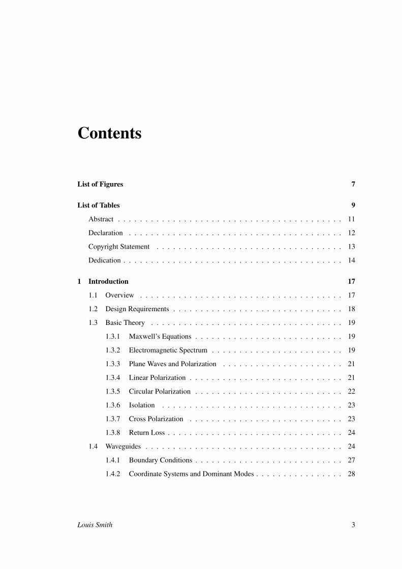
Contents
List of Figures 7
List of Tables 9
Abstract . . . . . . . . . . . . . . . . . . . . . . . . . . . . . . . . . . . . . . . . . 11
Declaration . . . . . . . . . . . . . . . . . . . . . . . . . . . . . . . . . . . . . . . 12
Copyright Statement . . . . . . . . . . . . . . . . . . . . . . . . . . . . . . . . . . 13
Dedication . . . . . . . . . . . . . . . . . . . . . . . . . . . . . . . . . . . . . . . . 14
1 Introduction 17
1.1 Overview . . . . . . . . . . . . . . . . . . . . . . . . . . . . . . . . . . . . . 17
1.2 Design Requirements . . . . . . . . . . . . . . . . . . . . . . . . . . . . . . . 18
1.3 Basic Theory . . . . . . . . . . . . . . . . . . . . . . . . . . . . . . . . . . . 19
1.3.1 Maxwell’s Equations . . . . . . . . . . . . . . . . . . . . . . . . . . . 19
1.3.2 Electromagnetic Spectrum . . . . . . . . . . . . . . . . . . . . . . . . 19
1.3.3 Plane Waves and Polarization . . . . . . . . . . . . . . . . . . . . . . 21
1.3.4 Linear Polarization . . . . . . . . . . . . . . . . . . . . . . . . . . . . 21
1.3.5 Circular Polarization . . . . . . . . . . . . . . . . . . . . . . . . . . . 22
1.3.6 Isolation . . . . . . . . . . . . . . . . . . . . . . . . . . . . . . . . . 23
1.3.7 Cross Polarization . . . . . . . . . . . . . . . . . . . . . . . . . . . . 23
1.3.8 Return Loss . . . . . . . . . . . . . . . . . . . . . . . . . . . . . . . . 24
1.4 Waveguides . . . . . . . . . . . . . . . . . . . . . . . . . . . . . . . . . . . . 24
1.4.1 Boundary Conditions . . . . . . . . . . . . . . . . . . . . . . . . . . . 27
1.4.2 Coordinate Systems and Dominant Modes . . . . . . . . . . . . . . . . 28
Louis Smith 3
CONTENTS
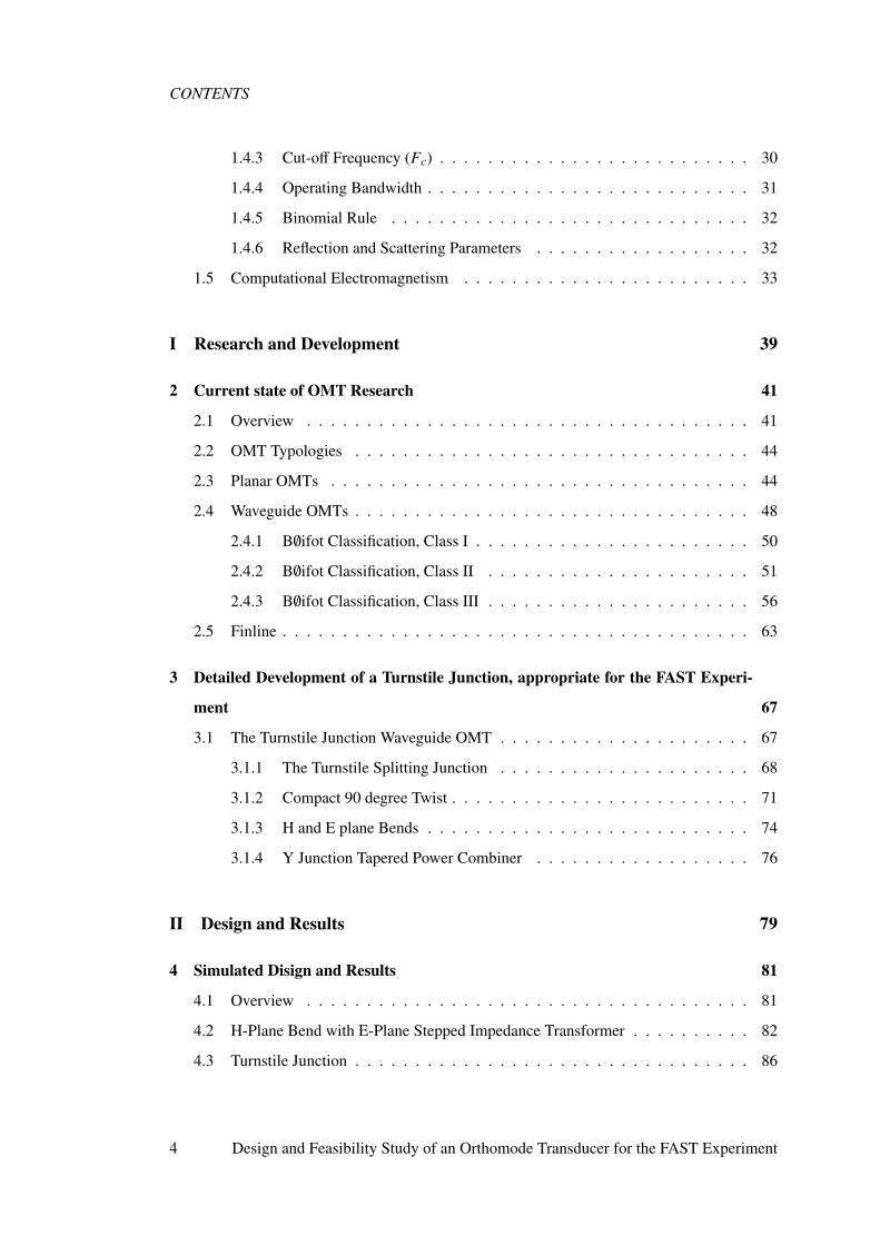
1.4.3 Cut-off Frequency (Fc) . . . . . . . . . . . . . . . . . . . . . . . . . . 30
1.4.4 Operating Bandwidth . . . . . . . . . . . . . . . . . . . . . . . . . . . 31
1.4.5 Binomial Rule . . . . . . . . . . . . . . . . . . . . . . . . . . . . . . 32
1.4.6 Reflection and Scattering Parameters . . . . . . . . . . . . . . . . . . 32
1.5 Computational Electromagnetism . . . . . . . . . . . . . . . . . . . . . . . . 33
I Research and Development 39
2 Current state of OMT Research 41
2.1 Overview . . . . . . . . . . . . . . . . . . . . . . . . . . . . . . . . . . . . . 41
2.2 OMT Typologies . . . . . . . . . . . . . . . . . . . . . . . . . . . . . . . . . 44
2.3 Planar OMTs . . . . . . . . . . . . . . . . . . . . . . . . . . . . . . . . . . . 44
2.4 Waveguide OMTs . . . . . . . . . . . . . . . . . . . . . . . . . . . . . . . . . 48
2.4.1 B∅ifot Classification, Class I . . . . . . . . . . . . . . . . . . . . . . . 50
2.4.2 B∅ifot Classification, Class II . . . . . . . . . . . . . . . . . . . . . . 51
2.4.3 B∅ifot Classification, Class III . . . . . . . . . . . . . . . . . . . . . . 56
2.5 Finline . . . . . . . . . . . . . . . . . . . . . . . . . . . . . . . . . . . . . . . 63
3 Detailed Development of a Turnstile Junction, appropriate for the FAST Experi-
ment 67
3.1 The Turnstile Junction Waveguide OMT . . . . . . . . . . . . . . . . . . . . . 67
3.1.1 The Turnstile Splitting Junction . . . . . . . . . . . . . . . . . . . . . 68
3.1.2 Compact 90 degree Twist . . . . . . . . . . . . . . . . . . . . . . . . . 71
3.1.3 H and E plane Bends . . . . . . . . . . . . . . . . . . . . . . . . . . . 74
3.1.4 Y Junction Tapered Power Combiner . . . . . . . . . . . . . . . . . . 76
II Design and Results 79
4 Simulated Disign and Results 81
4.1 Overview . . . . . . . . . . . . . . . . . . . . . . . . . . . . . . . . . . . . . 81
4.2 H-Plane Bend with E-Plane Stepped Impedance Transformer . . . . . . . . . . 82
4.3 Turnstile Junction . . . . . . . . . . . . . . . . . . . . . . . . . . . . . . . . . 86
4 Design and Feasibility Study of an Orthomode Transducer for the FAST Experiment

CONTENTS
4.4 Compact Ninety Degree Twist . . . . . . . . . . . . . . . . . . . . . . . . . . 89
4.5 Y Junction Tapered Power Combiner . . . . . . . . . . . . . . . . . . . . . . . 92
4.6 Simulated FAST OMT Design . . . . . . . . . . . . . . . . . . . . . . . . . . 95
5 Conclusions and Future Work 103
5.1 Conclusion . . . . . . . . . . . . . . . . . . . . . . . . . . . . . . . . . . . . 103
III Appendices 105
Louis Smith 5

CONTENTS
6 Design and Feasibility Study of an Orthomode Transducer for the FAST Experiment
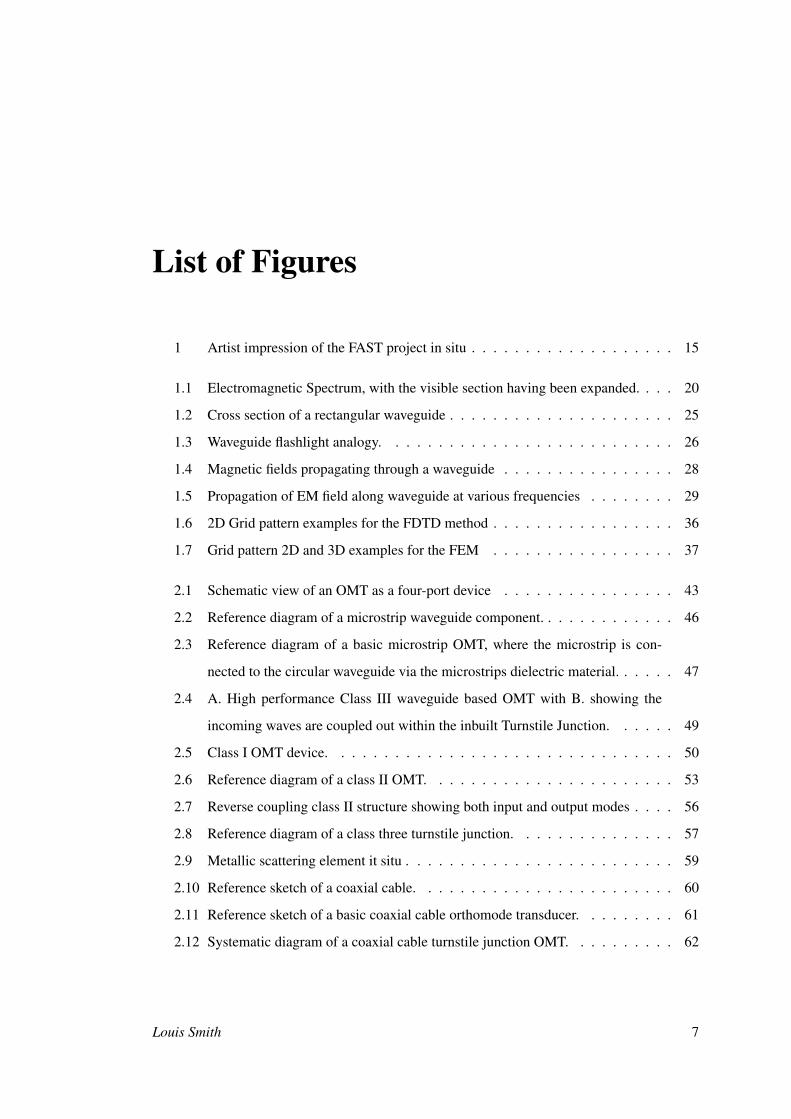
List of Figures
1 Artist impression of the FAST project in situ . . . . . . . . . . . . . . . . . . . 15
1.1 Electromagnetic Spectrum, with the visible section having been expanded. . . . 20
1.2 Cross section of a rectangular waveguide . . . . . . . . . . . . . . . . . . . . . 25
1.3 Waveguide flashlight analogy. . . . . . . . . . . . . . . . . . . . . . . . . . . 26
1.4 Magnetic fields propagating through a waveguide . . . . . . . . . . . . . . . . 28
1.5 Propagation of EM field along waveguide at various frequencies . . . . . . . . 29
1.6 2D Grid pattern examples for the FDTD method . . . . . . . . . . . . . . . . . 36
1.7 Grid pattern 2D and 3D examples for the FEM . . . . . . . . . . . . . . . . . 37
2.1 Schematic view of an OMT as a four-port device . . . . . . . . . . . . . . . . 43
2.2 Reference diagram of a microstrip waveguide component. . . . . . . . . . . . . 46
2.3 Reference diagram of a basic microstrip OMT, where the microstrip is con-
nected to the circular waveguide via the microstrips dielectric material. . . . . . 47
2.4 A. High performance Class III waveguide based OMT with B. showing the
incoming waves are coupled out within the inbuilt Turnstile Junction. . . . . . 49
2.5 Class I OMT device. . . . . . . . . . . . . . . . . . . . . . . . . . . . . . . . 50
2.6 Reference diagram of a class II OMT. . . . . . . . . . . . . . . . . . . . . . . 53
2.7 Reverse coupling class II structure showing both input and output modes . . . . 56
2.8 Reference diagram of a class three turnstile junction. . . . . . . . . . . . . . . 57
2.9 Metallic scattering element it situ . . . . . . . . . . . . . . . . . . . . . . . . . 59
2.10 Reference sketch of a coaxial cable. . . . . . . . . . . . . . . . . . . . . . . . 60
2.11 Reference sketch of a basic coaxial cable orthomode transducer. . . . . . . . . 61
2.12 Systematic diagram of a coaxial cable turnstile junction OMT. . . . . . . . . . 62
Louis Smith 7
LIST OF FIGURES
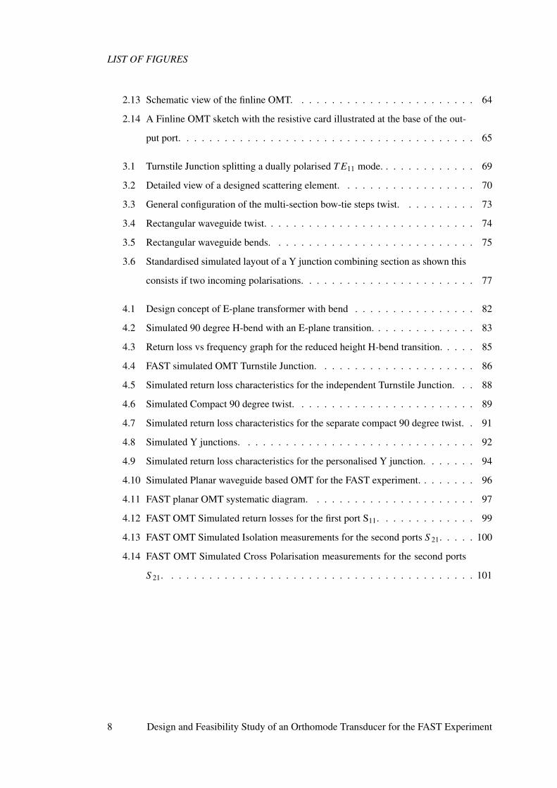
2.13 Schematic view of the finline OMT. . . . . . . . . . . . . . . . . . . . . . . . 64
2.14 A Finline OMT sketch with the resistive card illustrated at the base of the out-
put port. . . . . . . . . . . . . . . . . . . . . . . . . . . . . . . . . . . . . . . 65
3.1 Turnstile Junction splitting a dually polarised T E11 mode. . . . . . . . . . . . . 69
3.2 Detailed view of a designed scattering element. . . . . . . . . . . . . . . . . . 70
3.3 General configuration of the multi-section bow-tie steps twist. . . . . . . . . . 73
3.4 Rectangular waveguide twist. . . . . . . . . . . . . . . . . . . . . . . . . . . . 74
3.5 Rectangular waveguide bends. . . . . . . . . . . . . . . . . . . . . . . . . . . 75
3.6 Standardised simulated layout of a Y junction combining section as shown this
consists if two incoming polarisations. . . . . . . . . . . . . . . . . . . . . . . 77
4.1 Design concept of E-plane transformer with bend . . . . . . . . . . . . . . . . 82
4.2 Simulated 90 degree H-bend with an E-plane transition. . . . . . . . . . . . . . 83
4.3 Return loss vs frequency graph for the reduced height H-bend transition. . . . . 85
4.4 FAST simulated OMT Turnstile Junction. . . . . . . . . . . . . . . . . . . . . 86
4.5 Simulated return loss characteristics for the independent Turnstile Junction. . . 88
4.6 Simulated Compact 90 degree twist. . . . . . . . . . . . . . . . . . . . . . . . 89
4.7 Simulated return loss characteristics for the separate compact 90 degree twist. . 91
4.8 Simulated Y junctions. . . . . . . . . . . . . . . . . . . . . . . . . . . . . . . 92
4.9 Simulated return loss characteristics for the personalised Y junction. . . . . . . 94
4.10 Simulated Planar waveguide based OMT for the FAST experiment. . . . . . . . 96
4.11 FAST planar OMT systematic diagram. . . . . . . . . . . . . . . . . . . . . . 97
4.12 FAST OMT Simulated return losses for the first port S11. . . . . . . . . . . . . 99
4.13 FAST OMT Simulated Isolation measurements for the second ports S 21. . . . . 100
4.14 FAST OMT Simulated Cross Polarisation measurements for the second ports
S 21. . . . . . . . . . . . . . . . . . . . . . . . . . . . . . . . . . . . . . . . . 101
8 Design and Feasibility Study of an Orthomode Transducer for the FAST Experiment

List of Tables
1.1 OMT Requirements according to the FAST documentation . . . . . . . . . . . 19
5.1 OMT Requirements vs simulated results according to the FAST documentation 104
Louis Smith 9

LIST OF TABLES
10 Design and Feasibility Study of an Orthomode Transducer for the FAST Experiment
The University of Manchester
An Orthomode Transducer (OMT) is a waveguide structure capable of discriminating two in-
dependent signals of an orthogonal dominant mode incident upon its common port and to the
output port in its fundamental single mode form, therefore enabling the wave to be separated
in a passive manner. It is essential that this function is achieved whilst maintaining excellent
matching between all electrical ports and a high cross polarisation discrimination and isolation
to maintain the required independent signals.
The purpose of this thesis is to produce a feasibility study into the production of an Orthomode
Transducer for the FAST experiment; china’s contribution to the SKA, a global cosmological
collaboration which will operate with approximately a 34 percent bandwidth across the L-band
(0.95-1.45Ghz). With this in mind, a class three planar turnstile based OMT was investigated,
designed and then simulated using Ansofts HFSS 13, a commercially available package.
The method presented in the final design was formed through the use of a H-plane bend with an
integrated reduced height transition, a compact ninety degree twist, turnstile junction and a Y
junction recombining section all individually simulated during the course of this project. This
resulted in a highly, compact of total volume of 212mm3 uniquely planar low loss component;
average return losses -28dB, isolation of -49dB and cross polarization of -55dB. All having
been recorded across the chosen scaled W-band of 75-115GHz, with a view for this simulated
design to be manufactured and analysed using the University of Manchester’s VNA operating
at this frequency. These measurements represent a sufficient improvement on both the specified
thresholds stated in the FAST literature as well as other waveguide designs of similar size.
September 2012.
Louis Smith 11

Declaration
I do hereby declare that no portion of the work referred to in this thesis has been submitted in
support of an application for another degree or qualification of this or any other university or
other institute of learning.
12 Design and Feasibility Study of an Orthomode Transducer for the FAST Experiment

Copyright Statement
(i) Copyright in text of this thesis rests with the Author. Copies (by any process) either
in full, or of extracts, may be made only in accordance with instructions given by the
Author and lodged in the John Rylands University Library of Manchester. Details may
be obtained from the Librarian. This page must form part of any such copies made.
Further copies (by any process) of copies made in accordance with such instructions
may not be made without the permission (in writing) of the Author.
(ii) The ownership of any intellectual property rights which may be described in this thesis
is vested in The University of Manchester, subject to any prior agreement to the contrary,
and may not be made available for use by third parties without the written permission of
the University, which will prescribe the terms and conditions of any such agreement.
(iii) Further information on the conditions under which disclosures and exploitation may take
place is available from the Head of School of Physics and Astronomy.
Louis Smith 13

Dedication
To me, my family, friends and supervisor
without whom none of this would have been possible
14 Design and Feasibility Study of an Orthomode Transducer for the FAST Experiment
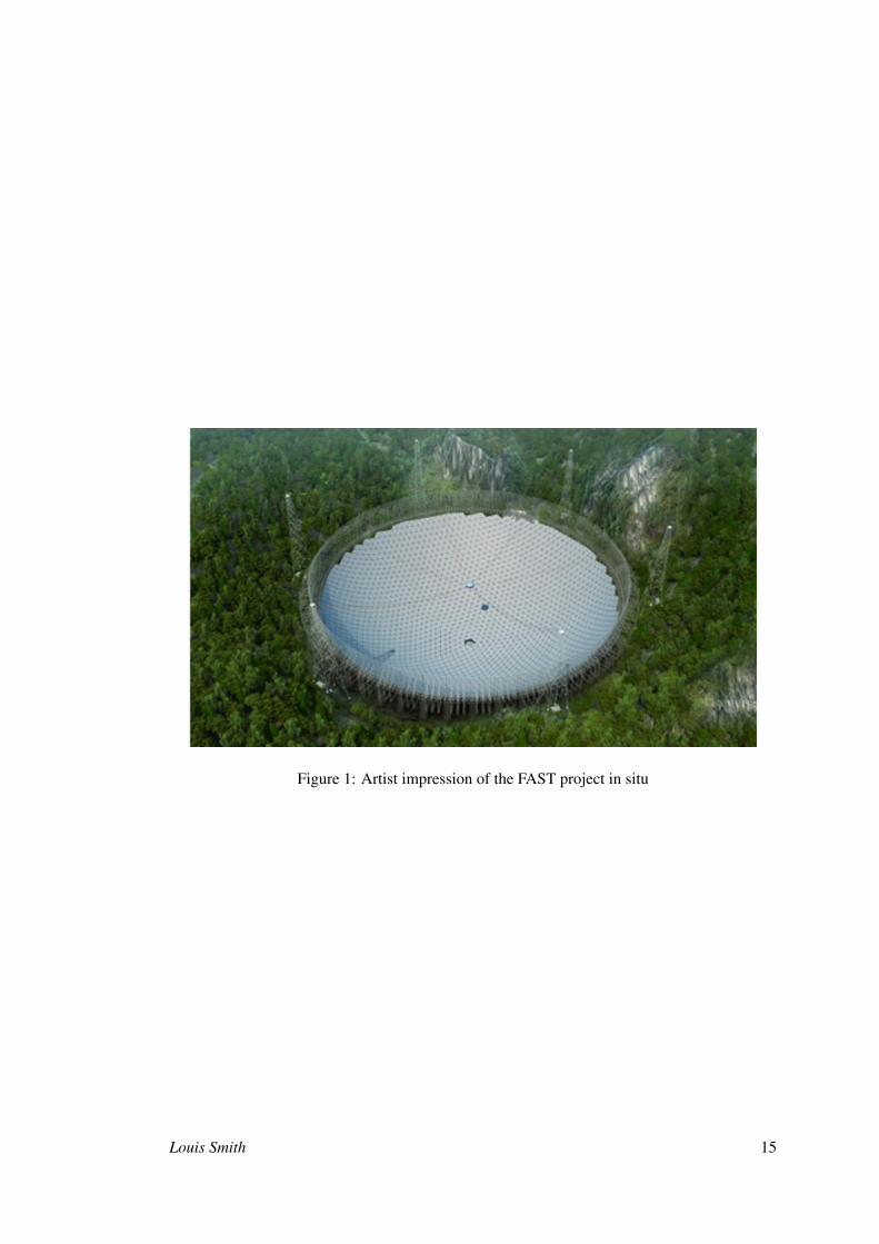
Figure 1: Artist impression of the FAST project in situ
Louis Smith 15

16 Design and Feasibility Study of an Orthomode Transducer for the FAST Experiment
1
Introduction
1.1 Overview
An Orthomode Transducer (OMT) is a passive device which has the task of separating orthog-
onal polarizations. It thus allows the use of two frequency channels simultaneously, enhancing
a systems capacity, whilst improving its versatility by permitting the structure to operate over
an improved bandwidth.
The intention of this masters thesis is to research, design and simulate the performance of an
Orthomode Transducer (OMT) operating with approximately a 34 percent bandwidth centred
at 1.45 GHz (the L-frequency band) using current waveguide technology. This concluding
design shall then be produced using a suitable production method and have its performance
compared to that of its computational cousin, enabling a comparison to be made (beyond the
scope of this thesis). This final design is required to provide excellent electrical matching be-
twixt all ports together with suitably high isolation, cross polarization and return losses with all
values specified for the wider application of the Five-hundred meter Aperture Spherical radio
Telescope (FAST), an astrophysical experiment which once built will be the largest single dish
radio telescope in the world[1].
Cosmology is the science of investigating the universe at its largest scales, to understand its
structural origins and evolution. In this vain FAST represents Chinas contribution to the inter-
Louis Smith 17
1: INTRODUCTION
national endeavour to build the Square Kilometre Array (SKA) is enabling copious
experimental investigations to be performed, at a combined cost of over 700 billion yuan. These
investigations will include but not be limited to; a spectroscopic survey of neutral hydrogen in
the Milky Way and other galaxies, detection of faint pulsars, conduct a visual examination for
the first shining stars or hearing the possible signals from other civilizations all of which are
being recorded for the first time or in greater detail than presently possible.[1]
There is an on-going requirement for antenna systems to operate across increasing bandwidths
in almost all applications from defence to as in this case radio astronomy. For this reason
OMTs with dual-polarization operation are key components in modern systems such as FAST.
While reviewing the literary sources, it was noted that an OMT (a passive device which acts
as means of separating or combines two orthogonal linearly polarized signals within the same
frequency band) can be referred to by various nom de plumes, including but not limited to, po-
larization diplexers[2], dual-mode transducers[4], orthomode junctions[4], or orthomode tees[5].
During this thesis I shall refer to this device as an orthomode transducer[6], due to its preva-
lence.
1.2 Design Requirements
Although the electrical and mechanical requisites of a design in respect to a microwave passive
assembly depend on the specific application, the common figure-of-merits of a dual-polarized
system are commonly low reflection losses measured through the use of a return loss measure-
ment, high polarization purity related to an isolation and cross polarization value, compactness
and reconfigurability[6]. The specified electrical specifications for this OMT are illustrated in
table 1 where the terms referred to shall be defined in more detail in sections 1.3.6, 1.3.7 and
1.3.8:
18 Design and Feasibility Study of an Orthomode Transducer for the FAST Experiment

1.3: BASIC THEORY
Table 1.1: OMT Requirements according to the FAST documentation[1]
1.3 Basic Theory
Some basic terminologies and concepts associated with the design and manufacture of a passive
device such, as an OMT, are relevant to this assignment; the expressions described in this
section shall be used throughout.
1.3.1 Maxwell’s Equations
Electromagnetic phenomena are all phenomena involving electric and magnetic fields propa-
gating through a vacuum or a dielectric medium. These physical phenomena were mathemat-
ically unified and described by Maxwell at the end of the 19th century then presented in their
modern rigorous form in 1887 by Heaviside, whose efforts to solve them resulted in the in-
troduction of vector notation provided its application to guided waves and transmission lines.
Maxwells equations have been proven at all frequencies and in any transmission system irre-
spective of complexity, therefore these equations are universally used in some form during the
modelling of any electromagnetic wave.
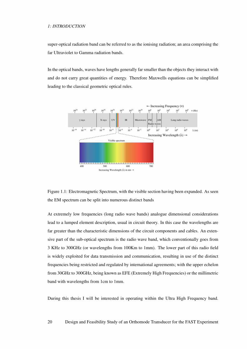
1.3.2 Electromagnetic Spectrum
The electromagnetic spectrum as introduced in figure 1.1 is a classification system for the
varying frequency bands therefore providing a useful method of separating the spectrum into
its associated energies, thus enabling the effects of EM radiation at various wavelength band
to be distinct. An initial natural division of the spectrum occurs at a point over which can be
observed through use of the human eye referred to as visible light (750-390nm spectrum) af-
ter which sub-optical and super-optical respectively refer to lower and higher frequencies. As
energy is directly proportional to frequency through Planck’s constant, the upper part of the
Louis Smith 19
1: INTRODUCTION
super-optical radiation band can be referred to as the ionising radiation; an area comprising the
far Ultraviolet to Gamma radiation bands.
In the optical bands, waves have lengths generally far smaller than the objects they interact with
and do not carry great quantities of energy. Therefore Maxwells equations can be simplified
leading to the classical geometric optical rules.
Figure 1.1: Electromagnetic Spectrum, with the visible section having been expanded. As seen
the EM spectrum can be split into numerous distinct bands
At extremely low frequencies (long radio wave bands) analogue dimensional considerations
lead to a lumped element description, usual in circuit theory. In this case the wavelengths are
far greater than the characteristic dimensions of the circuit components and cables. An exten-
sive part of the sub-optical spectrum is the radio wave band, which conventionally goes from
3 KHz to 300GHz (or wavelengths from 100Km to 1mm). The lower part of this radio field
is widely exploited for data transmission and communication, resulting in use of the distinct
frequencies being restricted and regulated by international agreements; with the upper echelon
from 30GHz to 300GHz, being known as EFE (Extremely High Frequencies) or the millimetric
band with wavelengths from 1cm to 1mm.
During this thesis I will be interested in operating within the Ultra High Frequency band.
20 Design and Feasibility Study of an Orthomode Transducer for the FAST Experiment
1.3: BASIC THEORY
Therefore, a microwave component shall be a prerequisite of the final design. In microwave
engineering it is usual to handle transmission line components and instruments with dimen-
sions similar to those in which they transmit. A lumped description similar to the standard
circuit theory is often not valid in these fields since the phase of a voltage or current may re-
sult in a significant change in the physical characteristics of the device. Therefore one must
often approach a microwave problem with Maxwells equations and their solutions, as such,
mathematical complexity must be expected.
1.3.3 Plane Waves and Polarization
A general plane wave has non-zero components in a plane orthogonal to the direction of prop-
agation. When a time harmonic E or H-plane wave is propagated in the positive z-direction
within free space the field can be described by either equation 1.1 or equation 1.2.
−→E =−→E te− jkz = [−→E xx +
−→E yy]e− jkz (1.1)
−→H = z−→E = zx−→E te− jkz = [−→E xx +−→E yy]e− jkz (1.2)
The polarization of a wave is determined by the characteristics of the E-field. It can be de-
scribed in terms of a desired co-polar component Eco which is parallel with the unit vector co
and an undesired cross-polar component Exp, which is laterally aligned to the cross-polar unit
vector xp and is orthogonal to co. Both co and xp are orthogonal to the direction of propagation
z as well as each other. Thus the total field can be expressed as equation 1.3.
E = [Eco + Expxp]e− jkz (1.3)
Using a scalar multiplication of the E field with the co and xp, the respective co-polar and
cross-polar components of the E-field (Et) can be calculated by the application of equation 1.4.
Eco = Etco Eco = Et xp (1.4)
1.3.4 Linear Polarization
If the start of the E-field vector oscillates in a straight line within the X-Y plane running per-
pendicular to the transmission of the wave; with the z-axis propagating in a linear polarization
Louis Smith 21
1: INTRODUCTION
it can be seen that the two field projections have a zero phase difference. While if the field is
y-directed, it can be defined as linearly polarised as expressed in equations, 1.5, 1.6 and 1.7.
uco = y xp = x (1.5)
Eco = Ety = Ey (1.6)
Exp = Et x = Ex (1.7)
An arbitrary linear polarization can be expressed in the co or cross polar unit vectors given in
equations 1.8 and 1.9:
co = cos(θx) + sin(θy) (1.8)
xp = sin(θx) + cos(θy) (1.9)
where, θ = π/2 represents the y-polarization and θ = 0 representing the x-polarization value.
1.3.5 Circular Polarization
A circularly polarized E-field vector can be thought of as a circularly polarized wave propagat-
ing along a circular helix in the direction of propagation. Such polarization will be either right
(RHC) or left hand (LHC) circularly polarized relating to whether its rotation is clockwise or
counter clockwise. RHC polarization can be expressed by the unit vector expressed in equation
1.10.
co =x − jy√
2(1.10)
It can therefore be observed that the y-component processes a phase factor
-j= e− j π2 compared to the x-component, resulting in the y-component being delayed by a quar-
ter of a period, giving an RHC polarized plane wave as described in equation 1.11.
The body of research over which this FAST experiment has been designed to operate and by
association the OMT described during this thesis, operates using a linear rather than circu-
lar model of polarization, therefore, from now on I shall only be concerned with a linearly
polarized system.
22 Design and Feasibility Study of an Orthomode Transducer for the FAST Experiment
1.3: BASIC THEORY
1.3.6 Isolation
The observed isolation between the two ports of an OMT represents one of the main criteria for
defining its performance. The isolation of a device is a unit of measurement defined in negative
dBs. Determined in the primary arm as the ratio between the dominant mode in the main arm
to the leakage to a secondary side arm, or vice-versa an isolation measurement represents the
undesired signal level on adjacent ports of a device. Therefore, the greater the isolation value
the lower interference experience from one signal on one port is present at the other.
If a received signal contains considerably less power than the transmitted signal it can be seen
that there is inadequate isolation between the output ports. Isolation greater than -35dB is
consequently usually required in the case of a dually polarized passive device such as an OMT,
where the two orthogonal polarizations being transmitted are required to be incoherent hence
excellent separation (or isolation) is essential.
1.3.7 Cross Polarization
Cross Polarization (sometimes referred to as X-pol) has been described in detail in [39] and
[40] and is a measurement of polarization orthogonal to those being discussed. These were
expertly defined by Luduig’s three definitions of which the 3rd is the most useful in this in-
stance; that the reference and cross polarization are deemed to be what one measured when
antenna pattern are taken in the usual manner[40]. For instance, in this case the field is defined
as horizontally polarized, therefore the cross polarized version of this wave would be vertically
polarized.
This term arises due to imperfections which may arise within an antenna systems polarization
resulting in two radiation patterns being presented: the co-pol (or desired polarisation compo-
nent) and the cross polarization component. Therefore, it can be seen that the lower the cross
polarization value, the higher the purity of the vacating wave.
The cross polarization is specified for an antenna system as a power level in dB’s. Cross
polarization greater than negative infinity indicates a level of polarization below optimum.
Louis Smith 23
1: INTRODUCTION
1.3.8 Return Loss
The third key measurement of an OMTs performance is the return loss; the input reflections
from an electrical port of the microwave device. A return loss below -15dB is necessary in most
common microwave designs[7]. However, a return loss below -20dB over most of the operating
band width is desirable. An average return loss -25dB is specified for this OMT design.
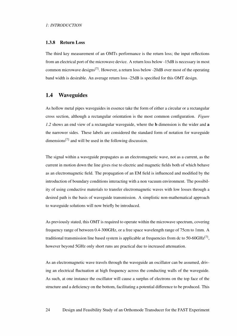
1.4 Waveguides
As hollow metal pipes waveguides in essence take the form of either a circular or a rectangular
cross section, although a rectangular orientation is the most common configuration. Figure
1.2 shows an end view of a rectangular waveguide, where the b dimension is the wider and a
the narrower sides. These labels are considered the standard form of notation for waveguide
dimensions[7] and will be used in the following discussion.
The signal within a waveguide propagates as an electromagnetic wave, not as a current, as the
current in motion down the line gives rise to electric and magnetic fields both of which behave
as an electromagnetic field. The propagation of an EM field is influenced and modified by the
introduction of boundary conditions interacting with a non vacuum environment. The possibil-
ity of using conductive materials to transfer electromagnetic waves with low losses through a
desired path is the basis of waveguide transmission. A simplistic non-mathematical approach
to waveguide solutions will now briefly be introduced.
As previously stated, this OMT is required to operate within the microwave spectrum, covering
frequency range of between 0.4-300GHz, or a free space wavelength range of 75cm to 1mm. A
traditional transmission line based system is applicable at frequencies from dc to 50-60GHz[7],
however beyond 5GHz only short runs are practical due to increased attenuation.
As an electromagnetic wave travels through the waveguide an oscillator can be assumed, driv-
ing an electrical fluctuation at high frequency across the conducting walls of the waveguide.
As such, at one instance the oscillator will cause a surplus of electrons on the top face of the
structure and a deficiency on the bottom, facilitating a potential difference to be produced. This
24 Design and Feasibility Study of an Orthomode Transducer for the FAST Experiment
1.4: WAVEGUIDES
motivates an electrical current to flow down the guide and thus the formation of a magnetic field
which will endeavour to circle around the created current.
Due to the presence of the waveguides metallic wall these fields cannot completely enclose the
current but combine, resulting in as the polarity slowly reverses the wave to travel down the
guide. A flux therefore occurs in the field facilitating the walls themselves to generate a current
further along the waveguide by induction, perpetuating the production of the electromagnetic
vectors further along the waveguide. As such, at any point along the guides internal wall one
would observe the electrons first cluster at the top then the bottom of the guide in a smooth
manner, this feature enables a waveguide system to be a highly efficient method to expedite the
radiation across the required space.
Figure 1.2: Cross section of a rectangular waveguide
There are three types of losses in conventional transmission lines: ohmic, dielectric and radia-
tion. The first of these, caused by currents flowing causing a resistance in the conductor making
up the transmission lines thus skin effects are formed; which themselves increase with escalat-
ing frequencies. Losses such as these tend to increase across the microwave region. Dielectric
losses are caused by the electric field acting on the molecules of the insulator and thereby
causing heating through molecular agitation. Radiation losses represent a loss of energy as an
electromagnetic wave propagates away from the surface of the transmission line conductor.
Losses on long runs of coaxial transmission line (the type most commonly used) give design-
Louis Smith 25
1: INTRODUCTION
ers cause for concern even at the low 0.4 to 5 GHz region due to increased losses. Power
handling capability also decreases at higher frequencies therefore, within higher microwave
bands where long runs make coaxial losses unacceptable or where high power levels would
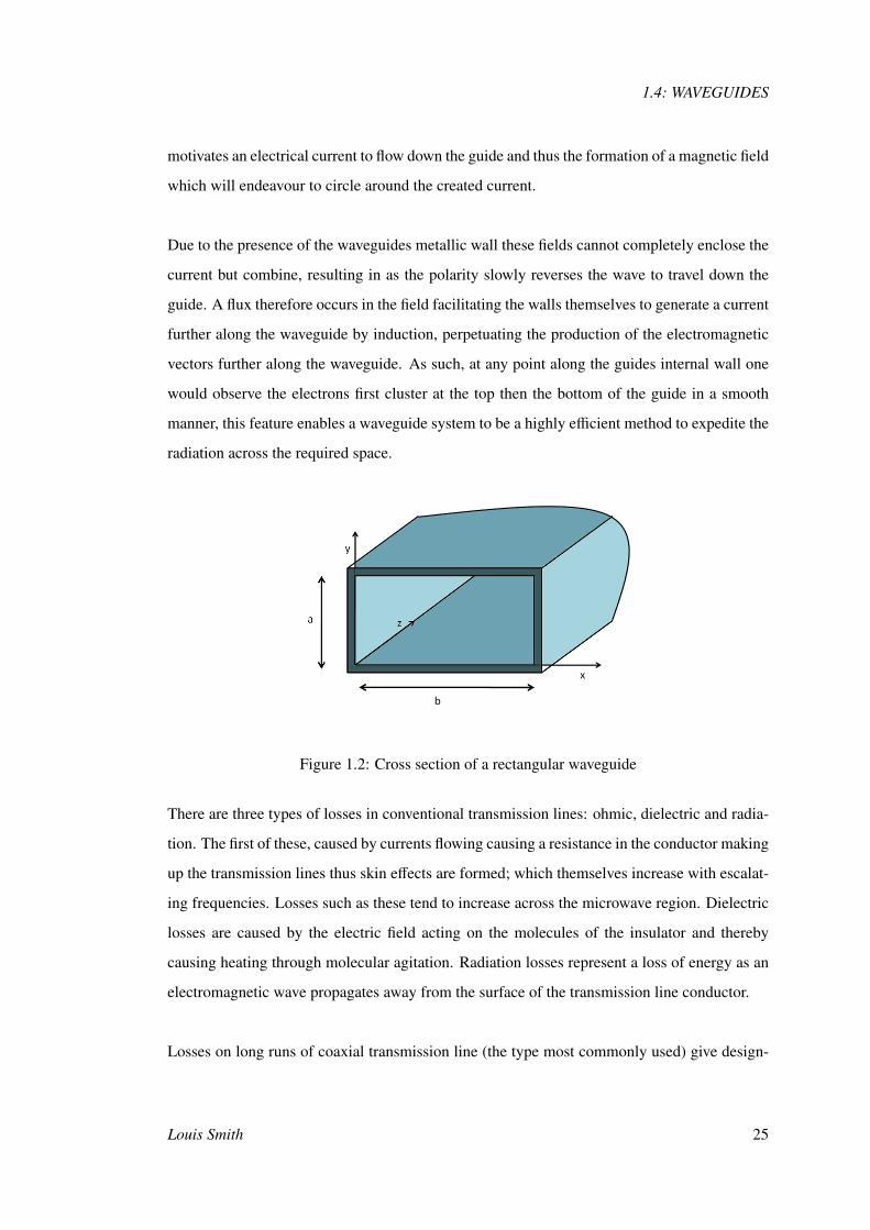
overheat the coaxial line, waveguides are preferable, for this design.
Figure 1.3: Waveguide flashlight analogy: in free space the beam spreads according to the
inverse square law.[7]
Waveguides are an imperative component within most modern OMT systems due to their field
focusing facilities. When an electromagnetic wave is propagated along a confining conducting
surface it is forced to obey Maxwells equations, while applying certain boundary conditions
at all points on the conducting walls. This device can be nicely illustrated with the flashlight
analogy in figure.1.3 where the flashlight serves as a RF source. In figure 1.3.a, this source is
radiated into free space and spreads out as a function of distance, with the intensity per unit
area at the destination (a wall) falling off as a function of distance D according to the inverse
square law.
26 Design and Feasibility Study of an Orthomode Transducer for the FAST Experiment
1.4: WAVEGUIDES
As shown in figure.1.3.b, compared to a freely propagating diffused beam over the same dis-
tance D, a waveguide confines the propagating waves inside a pipe, so intensifying the final
beam. While not perfect, this light pipe analogy with its mirrored walls neatly summarises
simply the operation of microwave waveguide. Thus, it can be considered that a waveguide is
analogous to an RF pipe.
The internal walls of a microwave waveguide are not, however, mirrored surfaces as in an op-
tical analogy (fibre-optical technology), but rather electrical conductors. Most waveguides are
made of aluminium, brass or copper, with efforts occasionally taken to reduce the ohmic losses
through the use of electroplating, a process requiring the internal surfaces to be plated with a
highly conductive material such as gold or silver, due to their lower resistivity in comparison
to other metallic substances[8].
1.4.1 Boundary Conditions
A TEM wave will not propagate in a perfect rectangular waveguide conductor by virtue of
certain boundary conditions[7] whilst the field in a waveguide propagates through air or an
inert dielectric gas in a manner similar to free-space propagation. This phenomenon of being
bound by the walls of the waveguide, implies certain conditions which must be met in order
for the wave to progress, the conditions are as follows:
1. The electric field must be orthogonal to the conductor.
2. The magnetic field must not be orthogonal to the surface of the waveguide.
A TEM modes boundary conditions do not meet these requirements as its magnetic field does
not propagate parallel to the surface of the conductor; so does not occur in a rectangular waveg-
uide. In order to satisfy these boundary conditions, two different types of propagation modes
are allowed:
1. Transverse Electric mode (TE mode)
2. Transverse Magnetic mode (TM mode)
Louis Smith 27
1: INTRODUCTION
Therefore, a transverse electric field results in the E-field propagating perpendicular to the con-
duction wall. This requirement is met by the use of a correctly coupled scheme at the input end
of the waveguide.
The second of these boundary condition requirements; stating that the magnetic field (H) must
not be orthogonal to the conductor surface, is fulfilled by applying a predefined constraint that
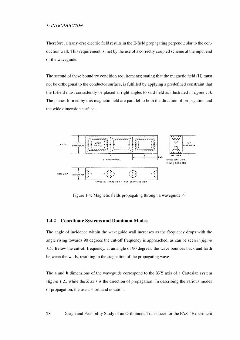
the E-field must consistently be placed at right angles to said field as illustrated in figure 1.4.
The planes formed by this magnetic field are parallel to both the direction of propagation and
the wide dimension surface.
Figure 1.4: Magnetic fields propagating through a waveguide [7]
1.4.2 Coordinate Systems and Dominant Modes
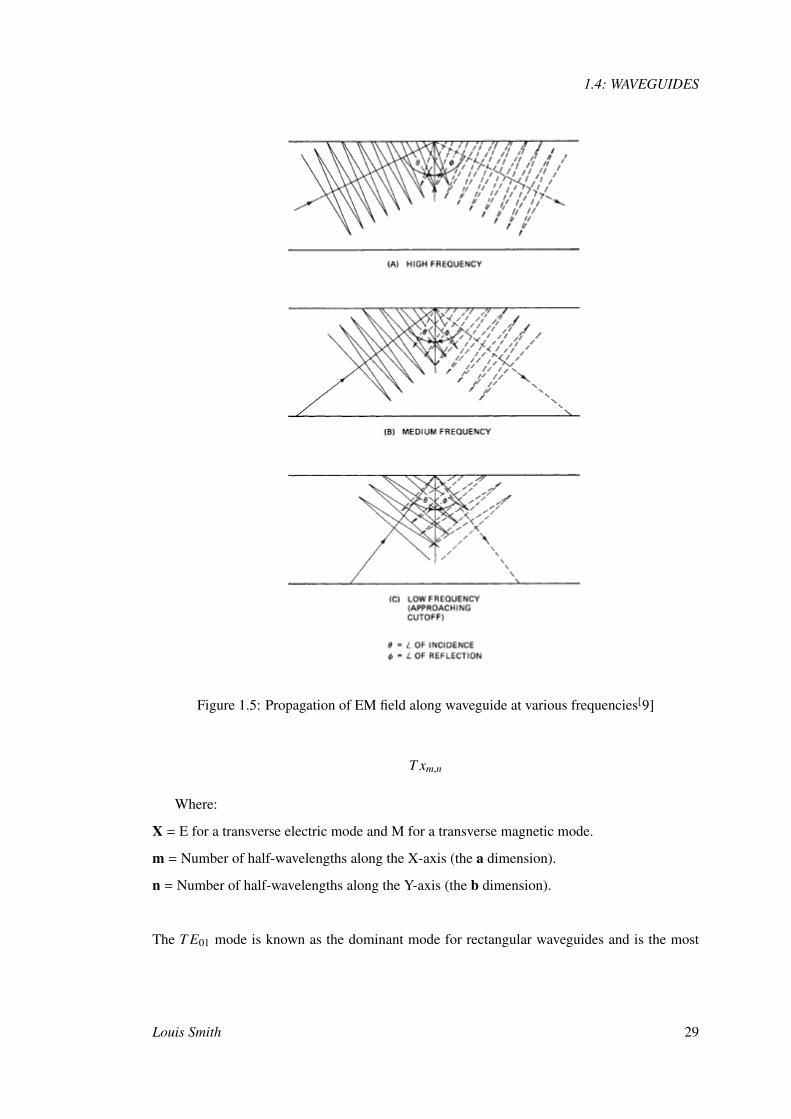
The angle of incidence within the waveguide wall increases as the frequency drops with the
angle rising towards 90 degrees the cut-off frequency is approached, as can be seen in figure
1.5. Below the cut-off frequency, at an angle of 90 degrees, the wave bounces back and forth
between the walls, resulting in the stagnation of the propagating wave.
The a and b dimensions of the waveguide correspond to the X-Y axis of a Cartesian system
(figure 1.2), while the Z axis is the direction of propagation. In describing the various modes
of propagation, the use a shorthand notation:
28 Design and Feasibility Study of an Orthomode Transducer for the FAST Experiment
1.4: WAVEGUIDES
Figure 1.5: Propagation of EM field along waveguide at various frequencies[9]
T xm,n
Where:
X = E for a transverse electric mode and M for a transverse magnetic mode.
m = Number of half-wavelengths along the X-axis (the a dimension).
n = Number of half-wavelengths along the Y-axis (the b dimension).
The T E01 mode is known as the dominant mode for rectangular waveguides and is the most
Louis Smith 29
1: INTRODUCTION
suitable mode for low-attenuation propagation in the Z axis. The nomenclature T E01 indi-
cates that there is one half-wavelength in the a dimension and zero half-wavelengths in the b
dimension.
1.4.3 Cut-off Frequency (Fc)
As the radiated wave propagates away from the input radiator, it resolves into two components
neither of which are parallel to the axis of propagation, or orthogonal to the walls. The compo-
nent along the waveguide axis is rapidly attenuated due to the waveguide boundary conditions.
This has been shown in figure 1.5, where for the sake of simplicity; only one component has
been shown. The propagation of a signal across a decreasing frequency (from A to C) in a
waveguide depends in part to the applied signal. As illustrated, the angle of incidence made
by a plane wave to the waveguide wall is a function of frequency. As this frequency drops, the
angle of incidence increases toward 90 degrees.
The propagation of a wave depends on the angle of incidence and its associated reflection
propagation. Indeed, both phase and group velocities are a function of the angle of incidence,
so much so that as the frequency drops to a point where the angle of incidence is 90 degrees,
the group velocity is zero and the concept of a phase velocity is meaningless. A general mode
equation based on the system in equation 1.11 can be formed.
1λ2
c= (
m2a
)2 + (n
2b)2 (1.11)
Where:
λc = The longest wavelength that will propagate, the cut-off waveguide.
a,b = The waveguide dimensions
m,n = The integers that define the number of half-wavelengths that will fit in the a and b di-
mensions respectively.
Therefore it can be seen from an extension of equation 1.11, that the longest TE-mode that can
propagate in a dominant (T E10) mode is given by equation 1.12.
λc = 2a (1.12)
30 Design and Feasibility Study of an Orthomode Transducer for the FAST Experiment
1.4: WAVEGUIDES
For which an expression for the cut-off frequency can be written:
Fc =c
2a(1.13)
Where:
Fc = Lowest frequency that will propagate in hertz, the cut-off frequency.
c = Speed of light (3x10⁸ m/s)
a = Wide waveguide dimensions.
1.4.4 Operating Bandwidth
The operating bandwidth of a waveguide and by association its corresponding OMT, is defined
between the cut-off frequency of the fundamental modes in the circular/ rectangular waveguides
(T E11 and T E10 respectively) and the cut-off frequency of the higher order modes propagating
within these structures.
It can be shown that the fundamental mode in a rectangular waveguide is the T E01 mode,
provided a > b with the bandwidth of a single-order mode for a rectangular waveguide being
dependent on the value of b. If a > 2b, the first higher-order mode is the T E20 with a cut-off
ratio fC,20 = 2 fC,10 propagating otherwise. In the case of b<a<2b the first higher order modes
(T E01) frequency is given by equation 1.14.
fC,20 =ab
fC,10 (1.14)
In practice almost all the standard waveguides have dimensions equal to a=2b[7] resulting in
the maximum bandwidth for the minimal ohmic costs, this configuration has been widely used
for previous OMT applications. In the case of the main port having an a = b configuration it
is customary for both orthogonal field configurations to propagate with the same properties,
constituting a very attractive structure for this application.
To design a broadband component, it is seen as necessary to produce transitions, such that,
only even higher order modes are present, due to the relative ease by which they can be com-
pensated. A waveguide device is defined as symmetrical if the different transitions cause the
Louis Smith 31
1: INTRODUCTION
dominant mode to generate only symmetrical (even-order) higher modes, while defined as non-
symmetrical if the dominant mode, in addition, produces odd-symmetrical higher order modes.
1.4.5 Binomial Rule
The binomial rule is generally recognised as a basis for reducing the reflection in certain waveg-
uide components operating over a substantial bandwidth. If several small bumps of the same
kind are spaced at quarter-wave intervals, their resultant reflection at frequencies near the fre-
quency of interest is (nearly minimized) by proportioning their individual reflections in the
ratio of a set of binominal coefficients. This rule provides a simplistic starting point for many
designs, even though most apply a flexible approach to its application resulting in the best re-
sults in both providing exceptional return losses with conventionally substantial bandwidth. In
applying the binominal rule, it is noted again that the reflection at each face is roughly pro-
portional to the square of the angle of a twist. Therefore, the angles at the respective faces are
made proportional to the square roots of a set of binomial coefficients. For a three face exam-
ple for instance, the binominal coefficients are 1 : 2 : 1, therefore, the square of the angles are
so proportioned and the angles are proportioned to 1 :√
(2) : 1. Giving the three angles as
26.4+37.2+26.4 = 90 degrees.
1.4.6 Reflection and Scattering Parameters
A significant parameter to describe the propagation through a transmission line is the reflection
parameter Γ(z). The generalised solution of the wave equations describes a wave travelling in
both a positive and negative z-direction, with the latter having the physical interpretation of the
reflected wave component. Reflection can also occur in a microwave network if an impedance
discontinuity is present, due to for instance a local discontinuity being present.
Since in general the point of interest is the efficiency of power transmitted from the input to the
output sections, defined as ports in black box description of any network with n ports can be
formed. In this case allowing for simplicity ai and b j to be respectively the incoming power at
the ith port and the outgoing power at the jth port, we can relate transmission T and the reflection
32 Design and Feasibility Study of an Orthomode Transducer for the FAST Experiment
1.5: COMPUTATIONAL ELECTROMAGNETISM
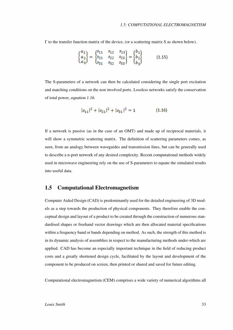
Γ to the transfer function matrix of the device, (or a scattering matrix S as shown below).
The S-parameters of a network can then be calculated considering the single port excitation
and matching conditions on the non involved ports. Lossless networks satisfy the conservation
of total power, equation 1.16.
If a network is passive (as in the case of an OMT) and made up of reciprocal materials, it
will show a symmetric scattering matrix. The definition of scattering parameters comes, as
seen, from an analogy between waveguides and transmission lines, but can be generally used
to describe a n-port network of any desired complexity. Recent computational methods widely
used in microwave engineering rely on the use of S-parameters to equate the simulated results
into useful data.
1.5 Computational Electromagnetism
Computer Aided Design (CAD) is predominantly used for the detailed engineering of 3D mod-
els as a step towards the production of physical components. They therefore enable the con-
ceptual design and layout of a product to be created through the construction of numerous stan-
dardised shapes or freehand vector drawings which are then allocated material specifications
within a frequency band or bands depending on method. As such, the strength of this method is
in its dynamic analysis of assemblies in respect to the manufacturing methods under-which are
applied. CAD has become an especially important technique in the field of reducing product
costs and a greatly shortened design cycle, facilitated by the layout and development of the
component to be produced on screen, then printed or shared and saved for future editing.
Computational electromagnetism (CEM) comprises a wide variety of numerical algorithms all
Louis Smith 33

1: INTRODUCTION
finding an approximate solution to the exact Maxwells equations over cells of finite dimensions
so the exact domain is divided, enabling a solution to be formulated, rather than solving exactly
the approximate equations given by the transmission line approximate. These methods can be
classified with respect to the form of hyperbolic Maxwells equations, they are based on either
differential or integral forms.
There are several methods, by which computational electromagnetism can be achieved. Many
of these approaches exhibit distinct features and advantages. Among these methods, there
are four of particular importance, all of which have been successfully used in the design of
passive components; the Method of Moments (MOM), Mode Matching method (MM), Finite-
Difference Time Domain method (FDTD) and finally the Finite-Element Method (FEM).
The most popular integral equation solver is the Method of Moments (MOM): requiring the
calculation of only the boundary values rather that the characteristics throughout the space,
therefore it is more efficient in terms of computational resources for problems with a small
surface area to volume ratio. Conceptually, MoM works by constructing a mesh of elements
over the modelled surface, however, for many problems this method is significantly less effi-
cient than corresponding volume-discretization methods, since boundary element formulations
typically give rise to fully populated matrices. This means that the storage requirements and
computational time grow according to the square of the unknowns. FEKO is a popular software
solver for radio frequency problems using the MoM solvers.
The mode matching method (MM) is a frequency-domain iterative integral method, based on
the notion that the field is expanded into analytical field eigen-functions under a region of anal-
ysis leading, when boundary conditions are imposed to an algebraically linear system. In order
to solve this problem, an inversion of a set of matrices formed at each boundary is required.
Eigenmodes[7] are found by solving Maxwells equations relying on the decomposition of the
electromagnetic fields into a basis set of local eigenmodes that exists in the cross-section of the
device. This necessitates the devices to be represented as a stack of layers where each layer is
uniform in the z-direction. Curved devices modelled with layers use a staircase approximation.
34 Design and Feasibility Study of an Orthomode Transducer for the FAST Experiment
1.5: COMPUTATIONAL ELECTROMAGNETISM
It can be seen from the mathematical formation that the algorithm is inherently bi-directional
using a scattering matrix technique to join the varying sections of the waveguide or modes
non-uniform structures.
In a typical waveguide, there are few guided modes (which propagate without coupling along
the waveguide) and an infinite number of radiation modes. This method is only suitable with
two or more separate regions. The µ -wave wizard software uses this MM technique. It has
been shown that the time scale and memory requirements square as a factor of the unknowns.
Consequently this method is limited in terms of the size of the cross-section for three dimen-
sional problems. A main limitation of this method is that, it is restricted to linear problems and
is inefficient in modelling structures requiring numerous modes. The Mode Matching method
is generally seen as a more efficient method of CAD than FDTD as it does not require dis-
cretization along the direction of propagation resulting in errors.
A differential equation solver is the most frequent method to solve Computational EM prob-
lems. Many commercial and university-developed tools using FDTD algorithms were devel-
oped during the early 1990s. FDTD belongs to a class of computational design tools known
as grid-based differential time-domain numerical methods. These take advantage of Maxwells
equations which are modified into a central difference equation, discretised then implemented
into software.
This involves the equations being organised into a matrix form which are then solved in a cyclic
manner (i.e. the electric field is solved at a given time, followed by the magnetic at the next
instance and so on). Since this method operates in the time-domain, solutions can operate over
a wide frequency range with a single solution run, provided that the intermediate time domains
steps are small enough to satisfy the Nyquist Shannon sampling theorem for the desired fre-
quency.
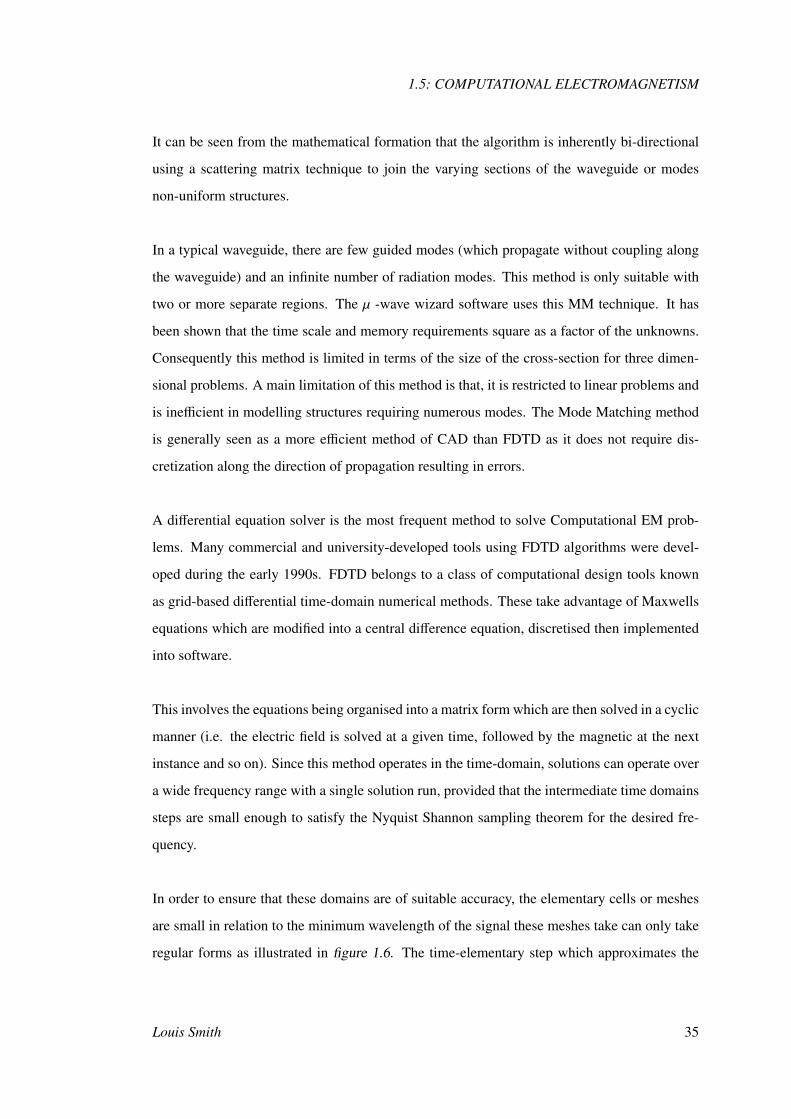
In order to ensure that these domains are of suitable accuracy, the elementary cells or meshes
are small in relation to the minimum wavelength of the signal these meshes take can only take
regular forms as illustrated in figure 1.6. The time-elementary step which approximates the
Louis Smith 35

1: INTRODUCTION
differential part of the derivative (with respect to time in the Maxwell equations) must satisfy
certain restraints i.e. that the ratio between the elementary cell dimensions and the light velocity
must be smaller than one. This leads directly to a solution with no need for matrix inversion.
The main disadvantage of this method is its time consuming nature and high computational
demand, as well as its order of magnitude inaccuracy in comparison to the MoM
Figure 1.6: 2D Grid pattern examples for the FDTD method
36 Design and Feasibility Study of an Orthomode Transducer for the FAST Experiment
1.5: COMPUTATIONAL ELECTROMAGNETISM
FEM is a frequency-domain method, similar to FDTD. The finite difference method is also
based on a discretisation of the domain, but it gives more flexibility than the previous methods
in choosing the element cells of the defining mesh. This may take the form of different shapes
within a single domain (resulting in better results being obtained with curved surfaces), as well
as not requiring the properties of the defined materials to be defined outside of the frequency
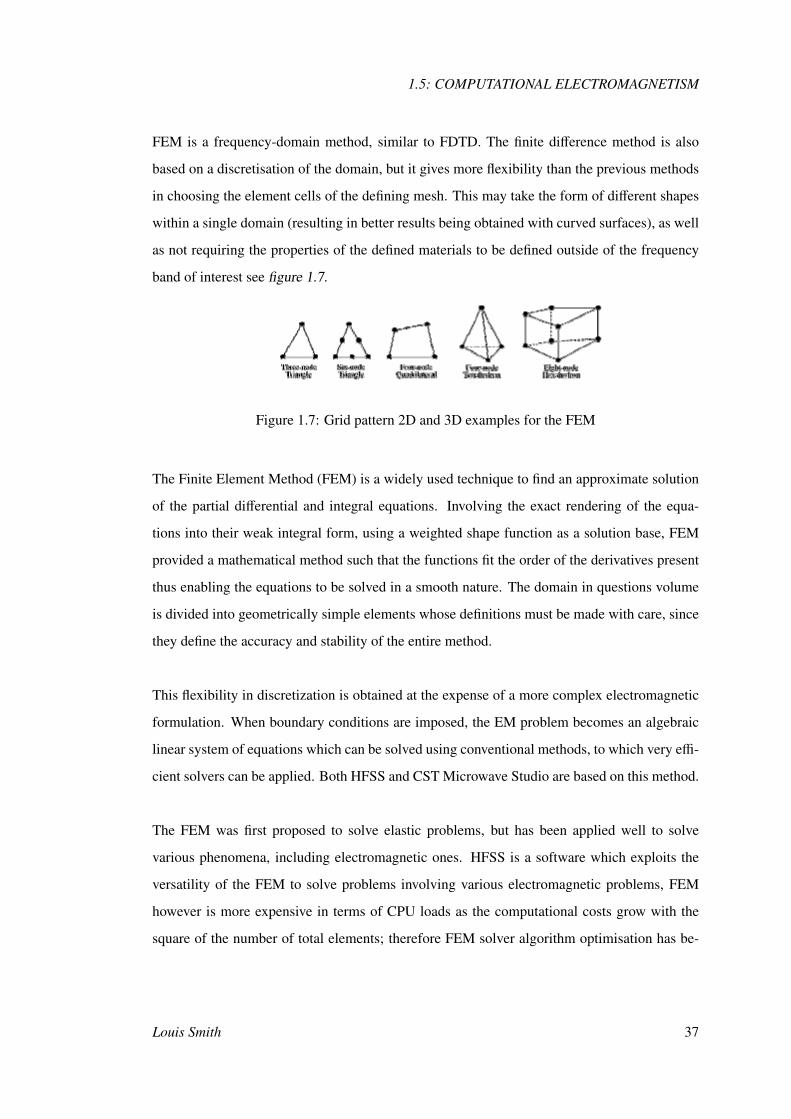
band of interest see figure 1.7.
Figure 1.7: Grid pattern 2D and 3D examples for the FEM
The Finite Element Method (FEM) is a widely used technique to find an approximate solution
of the partial differential and integral equations. Involving the exact rendering of the equa-
tions into their weak integral form, using a weighted shape function as a solution base, FEM
provided a mathematical method such that the functions fit the order of the derivatives present
thus enabling the equations to be solved in a smooth nature. The domain in questions volume
is divided into geometrically simple elements whose definitions must be made with care, since
they define the accuracy and stability of the entire method.
This flexibility in discretization is obtained at the expense of a more complex electromagnetic
formulation. When boundary conditions are imposed, the EM problem becomes an algebraic
linear system of equations which can be solved using conventional methods, to which very effi-
cient solvers can be applied. Both HFSS and CST Microwave Studio are based on this method.
The FEM was first proposed to solve elastic problems, but has been applied well to solve
various phenomena, including electromagnetic ones. HFSS is a software which exploits the
versatility of the FEM to solve problems involving various electromagnetic problems, FEM
however is more expensive in terms of CPU loads as the computational costs grow with the
square of the number of total elements; therefore FEM solver algorithm optimisation has be-
Louis Smith 37
1: INTRODUCTION
come one of the principle aims of software developers.
When the problem is simple, it is routine to use a mode matching method, due to rapidity of
analysis. However, due to the improved accuracy and computational capacity of modern com-
puters, this project uses a program based on the FEM method of analysis due to its perceived
flexibility and aptitude to overcome EM complications which are foreseen to occur within the
design of a relatively complex shape such as an OMT. OMTs are typically designed and opti-
mised using a commercial finite-element analysis software package such as Ansofts HFSS or
CST Microwave Studio, both industry standard simulation tools for 3D full-wave electromag-
netic field simulation. During this thesis I will use Ansofts HFSS 13 released in 2011 to define
the electromagnetic design which will be presented in the following chapters.
This choice is based on two considerations:
1. The availability of the licensing agreements
2. The proven accuracy of FEM in comparison to other defined methods
Due to the inherent difficulty associated with the design of a highly symmetric system such as
those associated with the OMT. The use of CAD programs has become commonplace with nu-
merous examples being forthcoming such as those in the references which all employ Ansofts
HFSS while demonstrate the use of the CST Microwave studio designs. It can also be seen that
the results obtained by the different FEM programs provide comparable overall results.
38 Design and Feasibility Study of an Orthomode Transducer for the FAST Experiment

Part I
Research and Development
Louis Smith 39

40 Design and Feasibility Study of an Orthomode Transducer for the FAST Experiment
2
Current state of OMT Research
2.1 Overview
In almost all applications, from radio astronomy to defence, an increase in demand for capacity
in satellite communication systems has brought about the need to operate over ever-increasing
bandwidths. Almost all wavelengths, including the millimetre bands, demand precise char-
acterisation of the amplitude, spectrum and polarization of the electromagnetic radiation is
essential. To further enhance capacity and versatility of an antenna system, dual-polarization
operation is often required, or in some cases, mandatory[10].
The conventional method of separating orthogonal polarizations for submillimeter receivers is
a grid of freestanding laterally standing wires, in which parallel and perpendicular E-field po-
larizations are reflected and transmitted respectively, depending on the initial grid composition.
This configuration necessitates the precise alignment of the associated feedhorns, thus careful
considerations are required to reduce vibrational damping.
Orthomode transducers are passive devices, which allow, through geometrical design, the trans-
duction of a generic dually polarized EM wave in two orthogonally polarized signals or vise-
versa. An OMT collocates in the radiometric chain between the feed horns and the receiving
system and must be designed to adapt both to the circular section of the antenna and to the
electric properties of the cabling, this system has numerous merits and demerits over a conven-
Louis Smith 41
2: CURRENT STATE OF OMT RESEARCH
tional wiregrid; these include:
Merits:
1. The use of an OMT can facilitate a receiver system to be simplistic and compact,
removing the need for an unwieldy wire grid configuration.
2. There are no requirements for calibrations to take place between grids recording their
respective polarizations.
3. Problems associated to the limited lifetimes of the wiregrid configuration can be
overcome.
4. In order to fit into existing dewars, a component must be compact; hence there is a
strong preference for the use of a waveguide based design rather than a much bulkier
alternative.
Demerits:
1. Fabrication and assembly of an OMT structure can prove problematic especially at
higher frequencies, as its small dimensions and tight tolerances pose a significant chal-
lenge with only few broadband OMT designs having been demonstrated to work suitably
at higher frequencies (above 100GHz).
2. An OMT must be formed with a suitable structure, since its performance has a signifi-
cant impact on the entire antenna feed system, therefore the design of a high performance
OMT requires the use of computer aided design software.
3. The joule losses of a waveguide must be included in the design aspects, in comparison
to an ideal wire grid configuration which processes almost no losses.
Due to the apparent strengths of an OMT’s design in comparison to current alternatives these
components are conventionally favoured (usually symmetric in nature) over traditional quasi-
optical wire grids for focal plane imaging arrays. From a system perspective, the key demerits
having been shown to be alleviated if mechanical robustness is made paramount and production
using a highly conductive electroforming finish (such as gold-plating) or alternative to reduce
the associated joule losses.[10]
42 Design and Feasibility Study of an Orthomode Transducer for the FAST Experiment
2.1: OVERVIEW
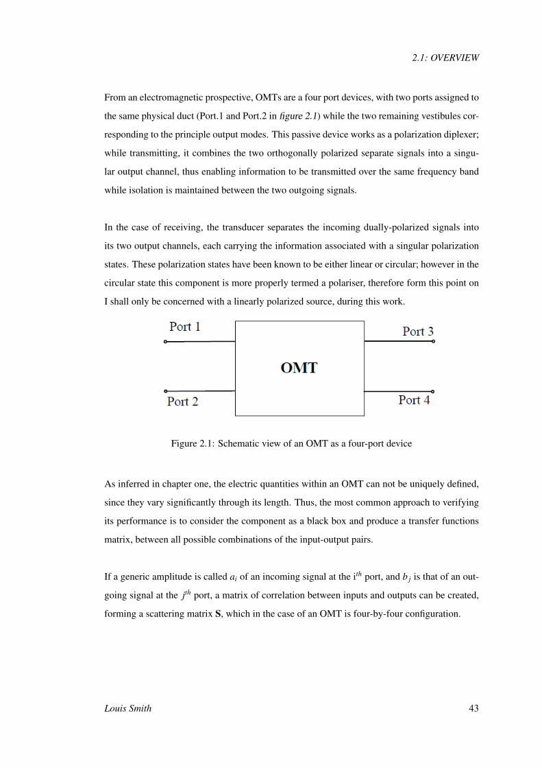
From an electromagnetic prospective, OMTs are a four port devices, with two ports assigned to
the same physical duct (Port.1 and Port.2 in figure 2.1) while the two remaining vestibules cor-
responding to the principle output modes. This passive device works as a polarization diplexer;
while transmitting, it combines the two orthogonally polarized separate signals into a singu-
lar output channel, thus enabling information to be transmitted over the same frequency band
while isolation is maintained between the two outgoing signals.
In the case of receiving, the transducer separates the incoming dually-polarized signals into
its two output channels, each carrying the information associated with a singular polarization
states. These polarization states have been known to be either linear or circular; however in the
circular state this component is more properly termed a polariser, therefore form this point on
I shall only be concerned with a linearly polarized source, during this work.
Figure 2.1: Schematic view of an OMT as a four-port device
As inferred in chapter one, the electric quantities within an OMT can not be uniquely defined,
since they vary significantly through its length. Thus, the most common approach to verifying
its performance is to consider the component as a black box and produce a transfer functions
matrix, between all possible combinations of the input-output pairs.
If a generic amplitude is called ai of an incoming signal at the ith port, and b j is that of an out-
going signal at the jth port, a matrix of correlation between inputs and outputs can be created,
forming a scattering matrix S, which in the case of an OMT is four-by-four configuration.
Louis Smith 43
2: CURRENT STATE OF OMT RESEARCH
The diagonal parameters S ii represents the reflection coefficients on the four ports; the
square of their module |S ii|2 defining a Power Loss (PLi) due to the electrical mismatch of port
i, while its mathematical reciprocal is the Return Loss (RLi). An ideal OMT should exhibit a
power loss parameter as close as possible to zero.
The quantities |S 41|−2 and |S 32|
−2 represent quantity of power of one polarisation mode reaching
the undesired port, defining therefore the cross polarizations, XPi j.
2.2 OMT Typologies
Varying types of OMTs exist with associated characteristics in terms of performances, working
frequency bands, geometry and production process. A useful classification for these systems
are based on the geometrical structure of the device, as presented in the following three sec-
tions:
2.3. Planar
2.4. Waveguide based
2.5. Finline
2.3 Planar OMTs
Planar OMTs use dielectric probes in rectangular or circular waveguides, representing the typ-
ical and most researched configuration since the early 2000s. This comprises four probes at
right angles within a cylindrical waveguide, after which the two orthogonal polarisations are
extracted by combining the signals from each pair of probes. This design is compact, simple to
construct and easily scaled to most frequencies.
44 Design and Feasibility Study of an Orthomode Transducer for the FAST Experiment
2.3: PLANAR OMTS
Due to advantages in integration, scalability and the low mass nature of a planar OMT com-
pared to other OMT methods[11], a planar transducer coupled to a corrugated horn is a good
solution for future astronomical research, in particular at sub-millimetre wavelengths such as
those involved in the investigation of the Cosmic Microwave Background.
The realisation of a high performance planar OMTs to achieve the stringent requirements of
new polarisation cosmology instruments, requires extreme precision and some corrective ex-
pedients, either to increment the bandwidth or to reduce the cross-polarisation, which in turn
requires higher costs.
Typical materials for the production of a planar device under standard lower frequency con-
ditions include metallic materials such as gold, copper or aluminium alloys, or at higher fre-
quencies a superconducting highly conductive materials, such as silicon nitrides or niobium are
commonly used.[12]
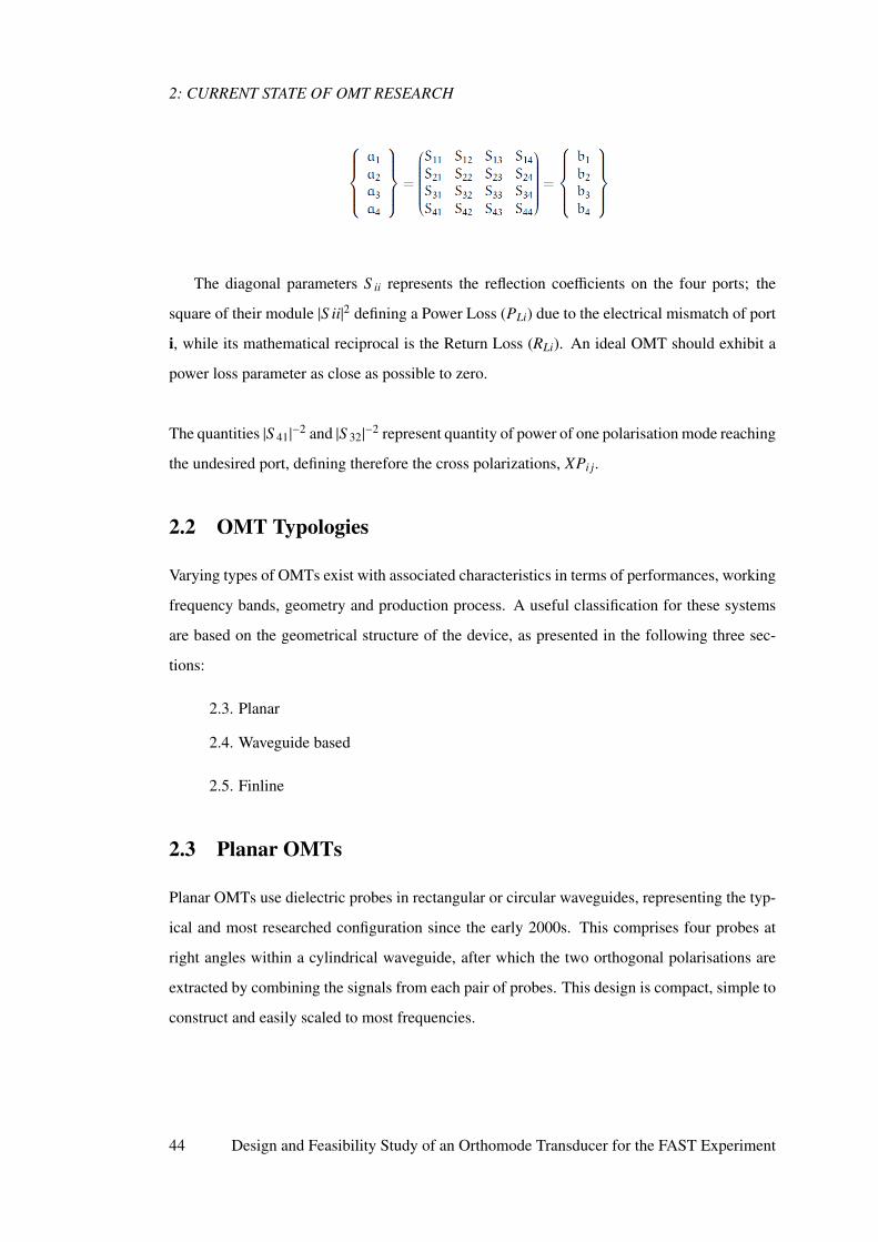
A microstrip, as in the one shown in figure.2.2 belongs to the family of planar devices used
largely in modern microwave applications. Comprising essentially a single-mode port, its sin-
gle fundamental mode supports modes propagating in the z-direction from a dc frequency band
upwards.
Louis Smith 45
2: CURRENT STATE OF OMT RESEARCH
Figure 2.2: Reference diagram of a microstrip waveguide component. As shown this is com-
prised of a number of different dielectric substrates [7]
It can be seen that a microstrip is formed by the combination of a conductive strip of width
w and thickness t placed within a substrate of relative dielectric constant ε and thickness h
grounded on one side by a conducting layer, this layer results in some major advantages over
more traditional production mediums. These include:
− Enabling fabrication using a low cost printed circuit board technology resulting in
good mechanical tolerances in the microwave range.
− It allows easy integration of elementary linear and nonlinear devices, making it possi-
ble to realise complex circuits directly on a single board (integrated circuits).
− It can be easily coupled with a square or circular waveguide to form an OMT as
illustrated in figure 2.4.
A major drawback associated however with the an OMT design based on the microstrip tech-
nology is associated with the medium in which the EM field must propagate being non-homogeneous.
This is different from other systems, where propagation is facilitated in either air or dielectric
material, but not both thus the propagation constant does not depend linearly on frequency
causing an extra distortion within the propagating wavepacket.
46 Design and Feasibility Study of an Orthomode Transducer for the FAST Experiment
2.3: PLANAR OMTS
The strip acts as a guide for the EM wave in the z-direction with the energy being concentrated
by the dielectric medium, in the region between the strip and the ground plane. Such is the
effect of this configuration as to emphasise the increasing dielectric constant. The fundamental
mode in this configuration is termed quasi-TEM, because the longitudinal component of the
associated EM field exists, but is very small compared to its transverse cousin.
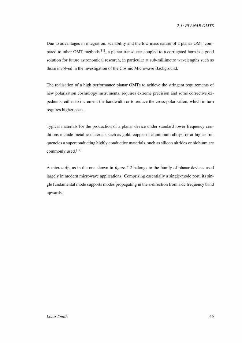
The most practical and widely used planar OMT configuration, figure 2.3, is formed by the
junction of two microstrip lines on a common substrate[7], with the strips intersected by another
at 90◦. These microstrip lines are typically enclosed by a metallic box connected electrically
to the waveguide walls where the lower side of the box representing the microstrips ground
plane, within a region inside the waveguide usually being removed to ensure conditions which
are favourable for optimum coupling.
Figure 2.3: Reference diagram of a basic microstrip OMT.[7]
In this configuration one side of the waveguide is typically short-circuited by a metallic plane
while on the other side the two orthogonal modes T E11V and T E11H , associated with ports one
and two, respectively, can propagate.
Louis Smith 47
2: CURRENT STATE OF OMT RESEARCH
The optimisation of this transition between the microstrip and a waveguide is currently a highly
researched topic, due to its structure being heavily used within the satellite communication in-
dustry. Although, the lack of symmetry in the polarisation plane does not provide high perfor-
mance and broadband operation, this configuration nevertheless has two major advantages:
− An OMT can be easily fabricated and network matched networks using present state
of the art microstrip technologies.
− It is very easy to accommodate on a microstrip the active circuitry required to effi-
ciently process the incoming radio frequency signals. Thus, on a microstrip card the
OMT, matching network, low noise amplifiers and wave integrated circuit technology
can all be facilitated without an appreciable degradation of the quality of the signal itself.
A typical performance for this type of OMT design has been recorded to be between 10-15
percent bandwidth with a minimum return loss of 15-20dB and an isolation characteristics of
typically 30-40dB.
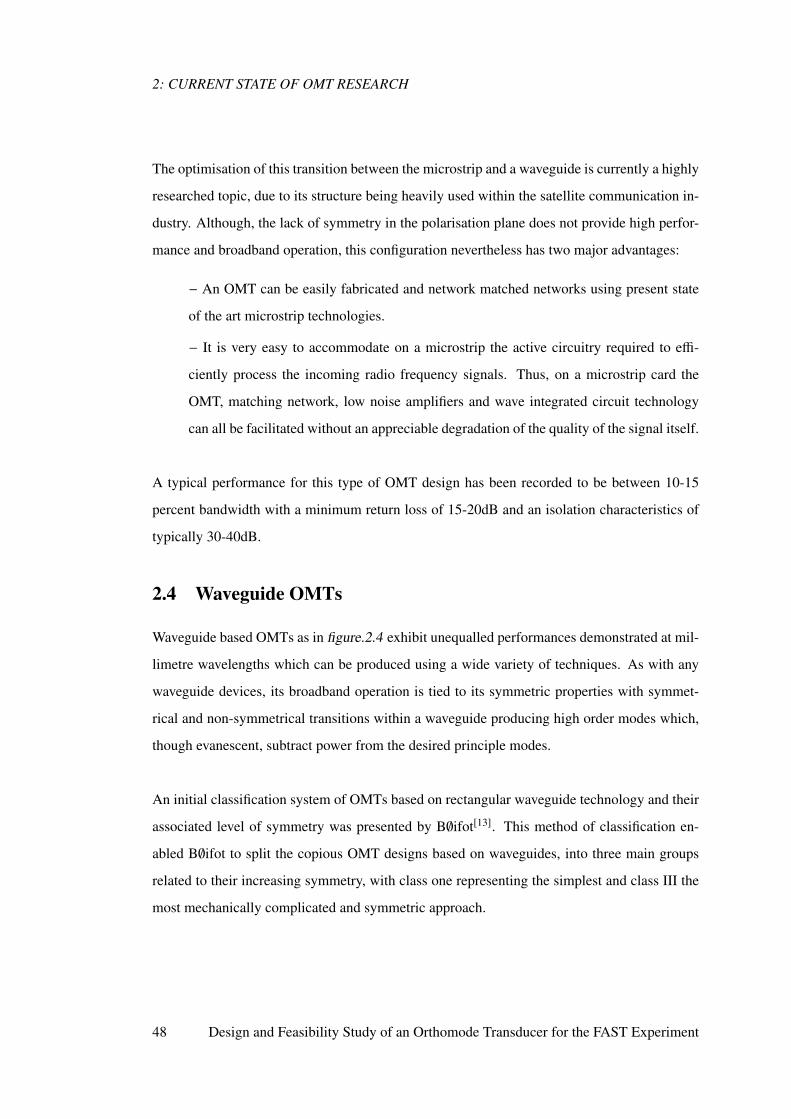
2.4 Waveguide OMTs
Waveguide based OMTs as in figure.2.4 exhibit unequalled performances demonstrated at mil-
limetre wavelengths which can be produced using a wide variety of techniques. As with any
waveguide devices, its broadband operation is tied to its symmetric properties with symmet-
rical and non-symmetrical transitions within a waveguide producing high order modes which,
though evanescent, subtract power from the desired principle modes.
An initial classification system of OMTs based on rectangular waveguide technology and their
associated level of symmetry was presented by B∅ifot[13]. This method of classification en-
abled B∅ifot to split the copious OMT designs based on waveguides, into three main groups
related to their increasing symmetry, with class one representing the simplest and class III the
most mechanically complicated and symmetric approach.
48 Design and Feasibility Study of an Orthomode Transducer for the FAST Experiment
2.4: WAVEGUIDE OMTS
Figure 2.4: High performance Class III waveguide based OMT[7]
Typically, the common port has a square or circular section, since it must host both vertical
and horizontal principle modes coming from its incoming source, while the output due to its
singular transverse mode has a standardised rectangular shape with a typical dimension ratio of
1:2 between the two faces due to its singular transverse mode. A major advantage to a circular
port is that can be directly joint to a feed horn waveguide, whilst a square input would require a
circular−to−square transition, which would potentially introduce a mismatch between an OMT
and its corresponding coupled device. Section transformers for circular to square to rectangular
standard ports, just like junctions, are of critical importance with good matching properties a
necessary for this reason.
The B∅ifot classification is a suitable and logical system as, for any waveguide OMT since
the broadband operation of the transducer is tied to its symmetric properties, therefore non-
symmetric transitions when present in the constituent OMT waveguides produce discontinu-
ities consequently higher order modes are produced, most of which are evanescent and do not
propagate. Uncompensated higher order modes however store reactive energy preventing the
broadband operation of the device, therefore the production of these higher order modes often
dictates the broadband isolation and input matching capacity of a waveguide device.
Hence it can be seen that several asymmetric OMTs have been designed to cover bandwidths
of less than 30 percent[13], whilst highly symmetric structures enabling the avoidance of higher
Louis Smith 49
2: CURRENT STATE OF OMT RESEARCH
order mode excitation enables a broad bandwidth (of 40 percent or more)[14]. The adoption
of symmetrical structures, such as a B∅ifot[15] or turnstile junction[16], improves the channel
isolation and return loss characteristics of the OMT, although at the cost of a greater mechanical
complexity. As a consequence of their symmetry, the isolation and cross-coupling in these
configurations are, in principle, infinite and zero respectively.
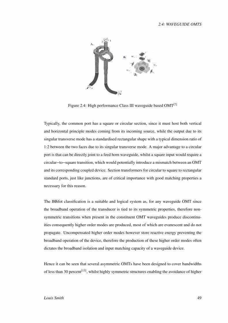
2.4.1 B∅ifot Classification, Class I
The first class of waveguide OMTs represents the simplest and most common approach con-
sisting of a main arm used for one mode and an orthogonal side arm. These resultant structures
are symmetric in respect to the primary mode yet not for the secondary, thus creating an asym-
metric device see figure 2.5.
Figure 2.5: Class I OMT, where port 1 represents the input common port while ports 2 and 3
are the output.[13]
Historically, these designs were driven by a desire to minimise the volume, mass and trans-
mission losses incurred in achieving polarization discrimination all within an undemanding
mechanical framework. Asymmetric OMTs are commonly used for polarization diplexing in
microwave applications due to their ease of design, with the performance of these structures
being limited in practice to a fractional bandwidth of 10 to 30 percent caused by the excitation
of higher order modes in the common arm by discontinuities caused through the construction
of symmetrical higher-order modes. These modes have their cut-offs within the frequency
range of operation, reducing the hypothetical performance, however, owing to cancelling ef-
fects, leakages to the side arm ideally does not occur.
50 Design and Feasibility Study of an Orthomode Transducer for the FAST Experiment
2.4: WAVEGUIDE OMTS
It is therefore possible to achieve a full broadband isolation for a mode in the main arm, how-
ever it has been observed that at higher bandwidths (approx. 30 percent)[17] an OMT based on
an asymmetric configuration, is burdened by a strong dispersion towards the lowest frequencies
and by a very faint attenuation of the T E11 and T M11 modes at the highest frequencies. Owing
to this non-symmetrical nature, the sidearm for this mode causes a configuration of imbalance,
thereby leading to the generation of odd-symmetrical modes. This non-symmetry also causes
the higher-order modes to leak to the main arm and negatively affect the polarization purity.
Thus it is difficult to achieve good isolation over a wide frequency scale for the mode in the
side arm, as well as low return loss. Several tuning screws or other reactive components have
been suggested[18] to achieve reasonable matching, however the use of these have shown to
result in a higher level of complexity removing one of the major advantages of this design, as
well as limiting the scalability over which a class I design may operate at higher frequencies
due to the the reactive components size becomes unsuitable.
The highest performing example of a class one OMT can be seen in [17] et al A. Dunning,
S. Srikanth and A.R. Kerr, where the resultant complexity resulting from a more symmetric
component would have meant considerable complication compared with the final class I asym-
metric designs. In this case a return loss of -24dB was achieved with an isolation characteristic
of 37dB across a 30 percent bandwidth.
2.4.2 B∅ifot Classification, Class II
A secondary class of OMT as defined by B∅ifot comprises a more complex configuration
whereby the sidearm is split into two symmetrical elements from the main as illustrated in
figure 2.6. As in class one, a field in the main arm sees a symmetrical device, therefore cou-
pling only to symmetrical higher-order modes, thus causing a removal of unwanted effects
resulting in natural broadband behaviour. Dissimilarly however, to group one OMTs a class
two configuration also observes a symmetrical splitting and combining junction in side arm.
These designs built on the ideas by Brain conducted at Marconi Research Laboratory[41] and
first reported in its true split block configuration by B∅ifot with coupling occurring from the
Louis Smith 51
2: CURRENT STATE OF OMT RESEARCH
main arm through two symmetrical H-planes bends to a sidearm where it is recombined con-
structively. The symmetrical nature of the splitting and combining junctions of the sidearm
enables good isolation over a wide frequency range within both the main and side arms.
There are three main subgroups within the class II division which have been developed for
broadband applications (fractional bandwidth ≥ 26 percent) in respect to both the millimetre
and sub-millimetre range:
− B∅ifot junction with septum and pins[2].
− B∅ifot junction with a double ridge[19].
− Reverse coupling structure[20].
These designs can prove to be complex to manufacture and spacious in size due to the presence
of the recombining side ports, while RF losses are higher for the recombined side port in
comparison to the through port.
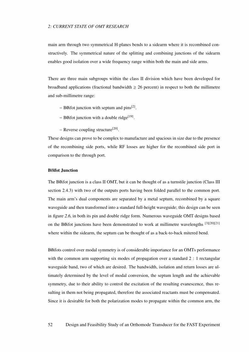
B∅ifot Junction
The B∅ifot junction is a class II OMT, but it can be thought of as a turnstile junction (Class III
section 2.4.3) with two of the outputs ports having been folded parallel to the common port.
The main arm’s dual components are separated by a metal septum, recombined by a square
waveguide and then transformed into a standard full-height waveguide; this design can be seen
in figure 2.6, in both its pin and double ridge form. Numerous waveguide OMT designs based
on the B∅ifot junctions have been demonstrated to work at millimetre wavelengths [3][20][21]
where within the sidearm, the septum can be thought of as a back-to-back mitered bend.
B∅ifots control over modal symmetry is of considerable importance for an OMTs performance
with the common arm supporting six modes of propagation over a standard 2 : 1 rectangular
waveguide band, two of which are desired. The bandwidth, isolation and return losses are ul-
timately determined by the level of modal conversion, the septum length and the achievable
symmetry, due to their ability to control the excitation of the resulting evanescence, thus re-
sulting in them not being propagated, therefore the associated reactants must be compensated.
Since it is desirable for both the polarization modes to propagate within the common arm, the
52 Design and Feasibility Study of an Orthomode Transducer for the FAST Experiment
2.4: WAVEGUIDE OMTS
higher order modes cut-off frequency is lower than that of the upper chosen frequency bands
edge.
The length of the side arms must be kept as close as possible to each other in order to ensure
coherent signal recombination within the power combiner. Phase errors manifest themselves
by means of constructive/destructive interference or beating at the side arm output. The usual
cause of this fault is manufacturing error. This can be remedied by a side arm power combiner
septum to compensate for minimal reflection, thus employing adiabatic transformation in its
guide height to match the output guide size.
Figure 2.6: Reference diagram of a class II OMT; A)With septum and pins OMT with septum
and pins, B) Shows the double ridge formation.
B∅ifot Junction with Septum and Pins
Within this conventional configuration the number, diameter and location of the pins are a
compromise between the tuning of the septum reactance, produced in the sidearm ports and
allowing a low impedance return path for the main-arm currents. From the main-arms perspec-
Louis Smith 53
2: CURRENT STATE OF OMT RESEARCH
tive, it is useful to think of the pins as a pair of short-circuit waveguide-stubs which are used
to tune out discontinuities from the sidearm junctions this design can be seen in figure.2.6.A.
While these pins provide an adequate match for the OMT, their small diameter and particular
placement result in the advanced complexity of assembly, therefore making them unsuitable
for scaling to terahertz frequencies.
The main and side-arm junctions are twofold symmetric about the vertical and horizontal guide
planes, thus, the T E11 and T M11 excitations can be avoided in the square common-arm of the
junction. Isolation above -40dB has been found to be common within this design with a return
loss of -20dB.[3][22]
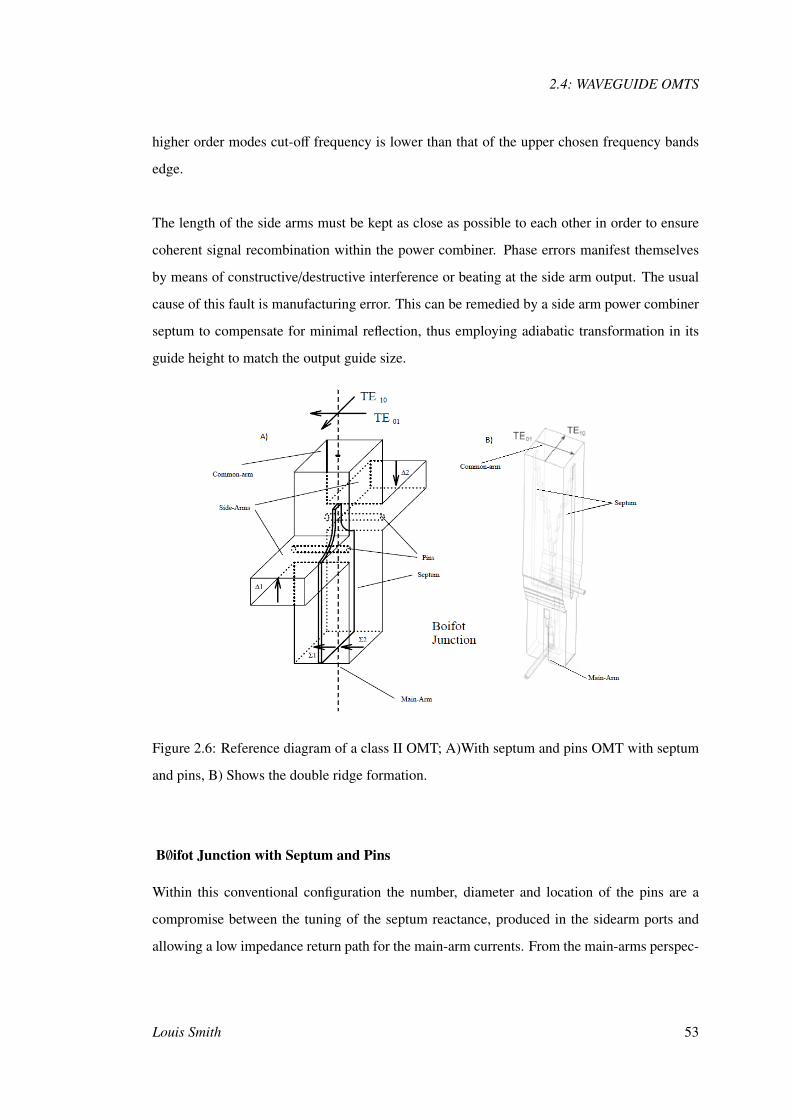
B∅ifot Junction with a double ridge
Numerous waveguide OMT designs based on the B∅ifot junction have been demonstrated to
work at the millimetre wavelengths, resulting in ever decreasing pin diameters with increas-
ing frequency. The complexity of assembling these, as previously stated, poses a significant
challenge for the reliable and cost-effective production of this device, especially at higher fre-
quencies. Other B∅ifot based designs with a thicker septum are however also possible, whereby
the pins are eliminated in favour of numerous of short capacitive steps, or alternatively stan-
dard multistep transitions on the side-arms as seen in figure.2.6.B. This results in the signal
being coupled to the sidearm then being transformed with an adiabatic taper and recombined;
this can be thought of as a thick septum from which the main-arm is carved. A configuration
allowing the use of this relatively compact and wideband E-plane bends with power combiners
is therefore allowed.
This design benefits from the mechanical realisation of the blocks giving a simplified assem-
bly, the alignment of the septum inside the waveguide however still remains critical. This
symmetric OMT achieves full waveguide band performance by limiting the excitation of T E11
and T M11 modes from the square common port. Isolation above -40dB has been found to
be achievable within this design with a return loss of -20dB, similar to the pin based B∅ifot
OMT.[3]
54 Design and Feasibility Study of an Orthomode Transducer for the FAST Experiment
2.4: WAVEGUIDE OMTS
Reverse-Coupling structure
The third subclass of this type is a reverse-coupling OMT method as shown in figure 2.7. This
type of OMT was developed at the Australia Telescope Facility by G. Moorey and P. Axtens for
the 77-177 GHz band in 2006. This conception processes a square waveguide input propagat-
ing two orthogonally linear polarized signals which enables, during any period, the wavelength
to be below the cut-off value. Beside the fundamental modes, some higher order modes can
propagate within the square waveguide frequency bands due to inherent discontinuities.
Higher order modes such as the T E11 and T M11 have the same cut-off frequency; therefore,
in theory these modes are excited by a discontinuity created in the aperture of the side arms.
However as long as the two-fold symmetry of the structure (a requirement of its class II status)
is maintained, these excitations can be limited. As with most class two OMTs its adopted
symmetry enables broadband operation allowing a bandwidth for this device of over 30 percent.[18]
The symmetric coupling structure of the common square waveguide arm splits the incoming
signal with opposite phases; the incoming T M11 signal into the two rectangular waveguide
side arms. Signals coupling to each sidearm are obtained with a broadband 90◦ hybrid coupler
realised with an E-plane branch line coupling structure. Isolation below -50dB has been found
to be common within this design with a return loss of -17dB, representing a current maximum.[21]
Louis Smith 55
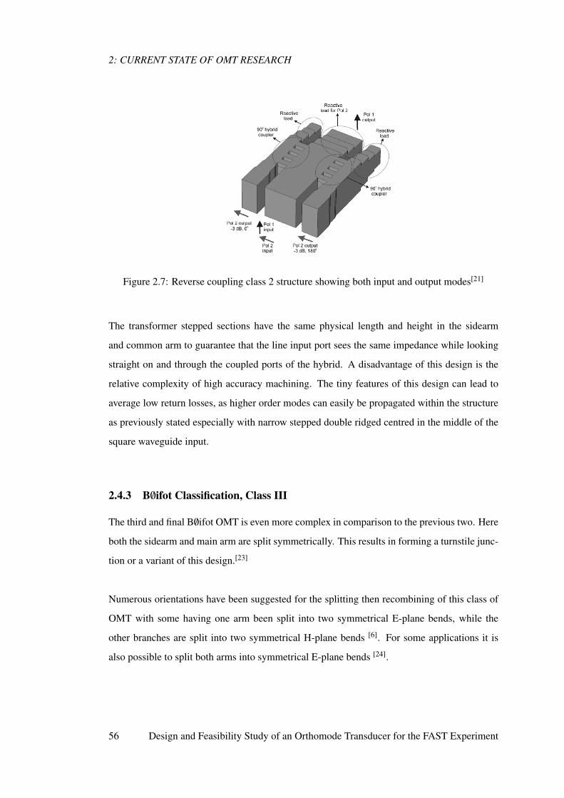
2: CURRENT STATE OF OMT RESEARCH
Figure 2.7: Reverse coupling class 2 structure showing both input and output modes[21]
The transformer stepped sections have the same physical length and height in the sidearm
and common arm to guarantee that the line input port sees the same impedance while looking
straight on and through the coupled ports of the hybrid. A disadvantage of this design is the
relative complexity of high accuracy machining. The tiny features of this design can lead to
average low return losses, as higher order modes can easily be propagated within the structure
as previously stated especially with narrow stepped double ridged centred in the middle of the
square waveguide input.
2.4.3 B∅ifot Classification, Class III
The third and final B∅ifot OMT is even more complex in comparison to the previous two. Here
both the sidearm and main arm are split symmetrically. This results in forming a turnstile junc-
tion or a variant of this design.[23]
Numerous orientations have been suggested for the splitting then recombining of this class of
OMT with some having one arm been split into two symmetrical E-plane bends, while the
other branches are split into two symmetrical H-plane bends [6]. For some applications it is
also possible to split both arms into symmetrical E-plane bends [24].
56 Design and Feasibility Study of an Orthomode Transducer for the FAST Experiment
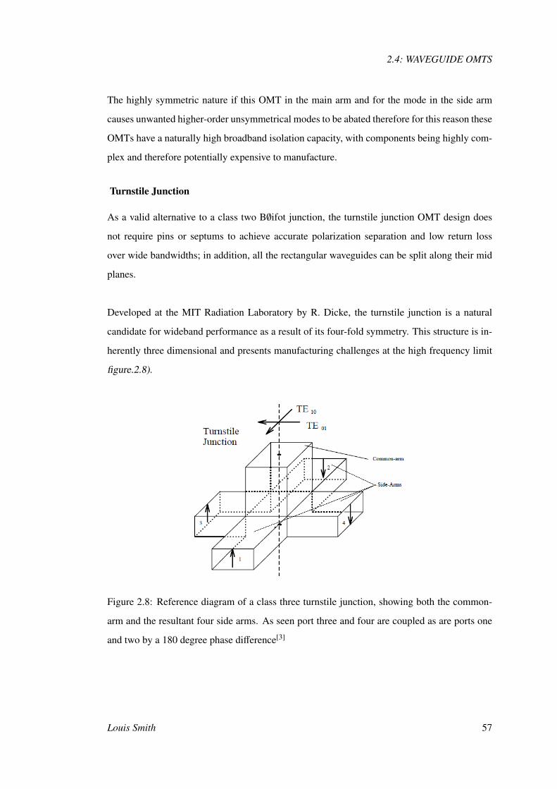
2.4: WAVEGUIDE OMTS
The highly symmetric nature if this OMT in the main arm and for the mode in the side arm
causes unwanted higher-order unsymmetrical modes to be abated therefore for this reason these
OMTs have a naturally high broadband isolation capacity, with components being highly com-
plex and therefore potentially expensive to manufacture.
Turnstile Junction
As a valid alternative to a class two B∅ifot junction, the turnstile junction OMT design does
not require pins or septums to achieve accurate polarization separation and low return loss
over wide bandwidths; in addition, all the rectangular waveguides can be split along their mid
planes.
Developed at the MIT Radiation Laboratory by R. Dicke, the turnstile junction is a natural
candidate for wideband performance as a result of its four-fold symmetry. This structure is in-
herently three dimensional and presents manufacturing challenges at the high frequency limit
figure.2.8).
Figure 2.8: Reference diagram of a class three turnstile junction, showing both the common-
arm and the resultant four side arms. As seen port three and four are coupled as are ports one
and two by a 180 degree phase difference[3]
Louis Smith 57
2: CURRENT STATE OF OMT RESEARCH
The turnstile junction processes a circular or square waveguide input port and four single-mode
rectangular waveguide outputs. This then enables the two orthogonal T E11 modes from the in-
put circular waveguide to be split equally into two T E10 modes by a scattering element as
shown in figure 2.4.B).
The first higher order mode generated in a circular waveguide input that can propagate in this
structure is T M11 mode enabling theoretically up to 70 percent bandwidth. On the other hand,
in a rectangular waveguide the first propagated higher order mode is that of the T E20 which
enables a bandwidth of 66 percent. Therefore, the maximum theoretical bandwidth that a turn-
stile junction can operate at just below one octave.[25]
A metallic tuning stub or scattering element is located at the base of the commonly circular ori-
entated waveguide, designed to maintain natural symmetry and enable an enhanced broadband
operation of above 40 percent to be achievable[25]. The shape and symmetry of this metallic el-
ement is critical. A square prism has been used as a tuning stub together with an E-plane bends
within a full height waveguide configuration obtaining a return loss better than 19dB [26] in the
18-26 GHz bend; a pyramid tuning stub orientation using a full height waveguide yielding a
return loss of -23dB respectively within the 9.2-12.4GHz band (30 percent bandwidth)[27][28].
A double cylindrical structure using a full height waveguide covering the 75-115GHz band
(38 percent bandwidth) achieved a return loss of -35dB thus improving the performance by
10dB over previous designs[6]. This orientation is illustrated in figure 2.9. these finding were
repeated during the course of this thesis providing similar results
58 Design and Feasibility Study of an Orthomode Transducer for the FAST Experiment

2.4: WAVEGUIDE OMTS
Figure 2.9: Metallic element it situ within the turnstile junction. As shown this can take the
form of a number of cylindrical varying steps located at the centre of the junction.[25]
Signals split by the turnstile junction exit opposite waveguides 180◦ out of phase. These signals
are then recombined in a power combiner which experiences a similar phase shift, implemented
using an E-plane Y junction as seen in figure2.4. The electrical lengths of the waveguides from
the turnstile to the power combiner are kept equal to maintain this phase variant.
The sidearm bends and impedance transformers are a compromise between two characteristics;
the ohmic and return losses. In addition, they are required to maintain the same electrical path
difference in order to maintain the appropriate phase difference once recombined. Isolation
above -35dB has been found to be common within this design.[6]
Coaxial Cable Turnstile Junction
Coaxial Cables are used in OMTs as a single mode port because its fundamental excitation has
a single polarization configuration avoiding the possibility of propagating two uncoupled sig-
nals. This structure enables the propagation of electromagnetic energy in the whole frequency
spectrum with the fundamental mode of propagation, (TEM) where both the electric and mag-
netic field vectors travel in a the plane orthogonal to the direction of propagation.
Figure 2.10 shows a common coaxial cable which usually comprises two materials: an homo-
geneous dielectric material and an inter-conducting medium to provide mechanical stability.
This structure is rotationally symmetric, therefore by applying a potential difference V between
Louis Smith 59
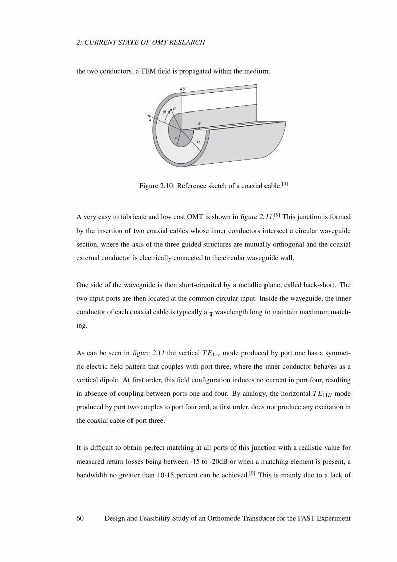
2: CURRENT STATE OF OMT RESEARCH
the two conductors, a TEM field is propagated within the medium.
Figure 2.10: Reference sketch of a coaxial cable.[9]
A very easy to fabricate and low cost OMT is shown in figure 2.11.[9] This junction is formed
by the insertion of two coaxial cables whose inner conductors intersect a circular waveguide
section, where the axis of the three guided structures are mutually orthogonal and the coaxial
external conductor is electrically connected to the circular waveguide wall.
One side of the waveguide is then short-circuited by a metallic plane, called back-short. The
two input ports are then located at the common circular input. Inside the waveguide, the inner
conductor of each coaxial cable is typically a 14 wavelength long to maintain maximum match-
ing.
As can be seen in figure 2.11 the vertical T E11v mode produced by port one has a symmet-
ric electric field pattern that couples with port three, where the inner conductor behaves as a
vertical dipole. At first order, this field configuration induces no current in port four, resulting
in absence of coupling between ports one and four. By analogy, the horizontal T E11H mode
produced by port two couples to port four and, at first order, does not produce any excitation in
the coaxial cable of port three.
It is difficult to obtain perfect matching at all ports of this junction with a realistic value for
measured return losses being between -15 to -20dB or when a matching element is present, a
bandwidth no greater than 10-15 percent can be achieved.[9] This is mainly due to a lack of
60 Design and Feasibility Study of an Orthomode Transducer for the FAST Experiment
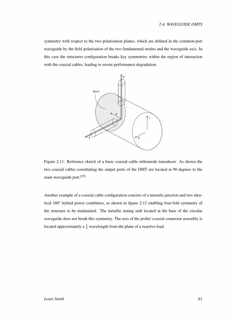
2.4: WAVEGUIDE OMTS
symmetry with respect to the two polarisation planes, which are defined in the common-port
waveguide by the field polarisation of the two fundamental modes and the waveguide axis. In
this case the structures configuration breaks key symmetries within the region of interaction
with the coaxial cables, leading to severe performance degradation.
Figure 2.11: Reference sketch of a basic coaxial cable orthomode transducer. As shown the
two coaxial cables constituting the output ports of the OMT are located at 90 degrees to the
main waveguide port.[29]
Another example of a coaxial cable configuration consists of a turnstile junction and two iden-
tical 180◦ hybrid power combiners, as shown in figure 2.12 enabling four-fold symmetry of
the structure to be maintained. The metallic tuning stub located at the base of the circular
waveguide does not break this symmetry. The axis of the probe/ coaxial connector assembly is
located approximately a 14 wavelength from the plane of a reactive load.
Louis Smith 61
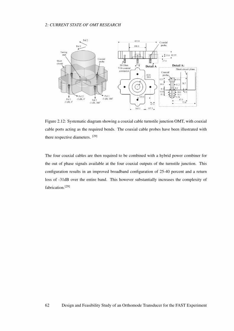
2: CURRENT STATE OF OMT RESEARCH
Figure 2.12: Systematic diagram showing a coaxial cable turnstile junction OMT, with coaxial
cable ports acting as the required bends. The coaxial cable probes have been illustrated with
there respective diameters. [29]
The four coaxial cables are then required to be combined with a hybrid power combiner for
the out of phase signals available at the four coaxial outputs of the turnstile junction. This
configuration results in an improved broadband configuration of 25-40 percent and a return
loss of -31dB over the entire band. This however substantially increases the complexity of
fabrication.[29]
62 Design and Feasibility Study of an Orthomode Transducer for the FAST Experiment
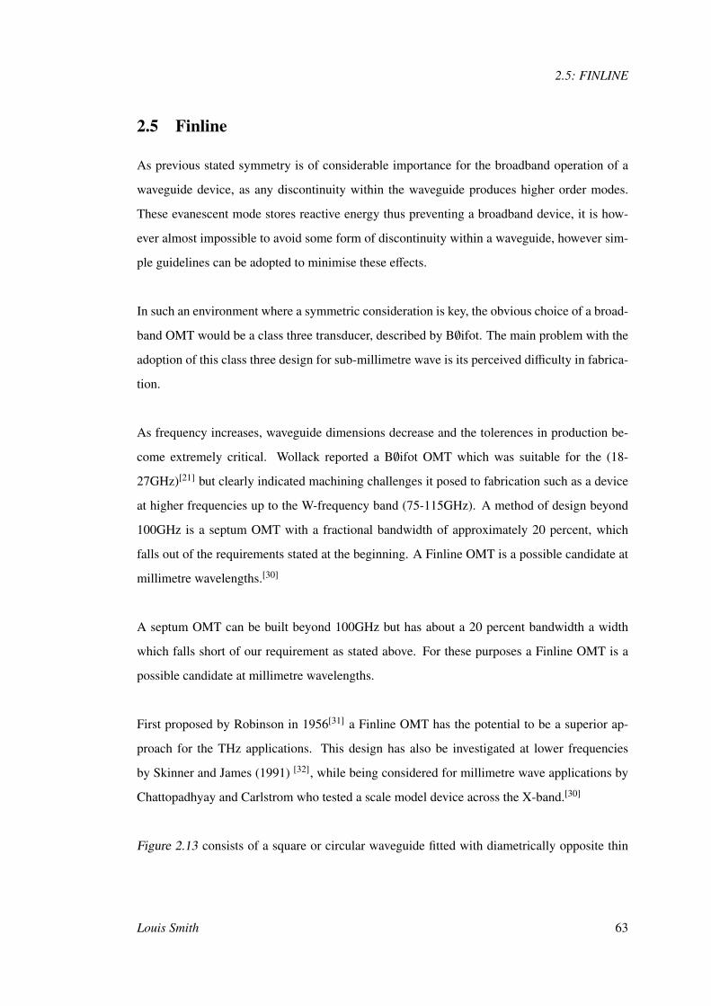
2.5: FINLINE
2.5 Finline
As previous stated symmetry is of considerable importance for the broadband operation of a
waveguide device, as any discontinuity within the waveguide produces higher order modes.
These evanescent mode stores reactive energy thus preventing a broadband device, it is how-
ever almost impossible to avoid some form of discontinuity within a waveguide, however sim-
ple guidelines can be adopted to minimise these effects.
In such an environment where a symmetric consideration is key, the obvious choice of a broad-
band OMT would be a class three transducer, described by B∅ifot. The main problem with the
adoption of this class three design for sub-millimetre wave is its perceived difficulty in fabrica-
tion.
As frequency increases, waveguide dimensions decrease and the tolerences in production be-
come extremely critical. Wollack reported a B∅ifot OMT which was suitable for the (18-
27GHz)[21] but clearly indicated machining challenges it posed to fabrication such as a device
at higher frequencies up to the W-frequency band (75-115GHz). A method of design beyond
100GHz is a septum OMT with a fractional bandwidth of approximately 20 percent, which
falls out of the requirements stated at the beginning. A Finline OMT is a possible candidate at
millimetre wavelengths.[30]
A septum OMT can be built beyond 100GHz but has about a 20 percent bandwidth a width
which falls short of our requirement as stated above. For these purposes a Finline OMT is a
possible candidate at millimetre wavelengths.
First proposed by Robinson in 1956[31] a Finline OMT has the potential to be a superior ap-
proach for the THz applications. This design has also be investigated at lower frequencies
by Skinner and James (1991) [32], while being considered for millimetre wave applications by
Chattopadhyay and Carlstrom who tested a scale model device across the X-band.[30]
Figure 2.13 consists of a square or circular waveguide fitted with diametrically opposite thin
Louis Smith 63
2: CURRENT STATE OF OMT RESEARCH
tapered metallic fins. In this configuration, the dominant mode, whose electric field is parallel
to the fins, is gradually transformed to the Finline mode whose energy is essentially confined
into a narrow gap between the fins located at the centre of the waveguide. This energy can then
be removed from the waveguide by curving the finline and bringing it out through the sidewall
of the guide.
Figure 2.13: Schematic view of the Finline OMT; A) illustrated the overall design consisting
of a thin metallic fin set inside a waveguide inorder to split the incoming dually polarised
input wavefront, B) illustrates the thin metallic fins set inside a circular or square waveguide.
Conventional resistive layers are used to suppress the excitation of unwanted modes (region
pointed by arrow) [31]
The mode which is polarized orthogonal to the fins passes through the guide virtually unper-
turbed with a sufficiently thin fin, enabling fabrication at milli-metric frequencies with a higher
level of ease than either class two or class three OMT, thus it is sometimes seen as more viable
in these bands.
Within the Chattopadhyay design[30], the fins were realised as two separate metallic plates held
at the proper separation with alignment pins. This design was scaled to a design of 1THz with
a final gap of 5µm.
Conventional Finline OMTs use a resistive card seen in figure 2.14 as a means of suppressing
the excitation of unwanted higher order modes simulated by the termination of the fins. It has
64 Design and Feasibility Study of an Orthomode Transducer for the FAST Experiment
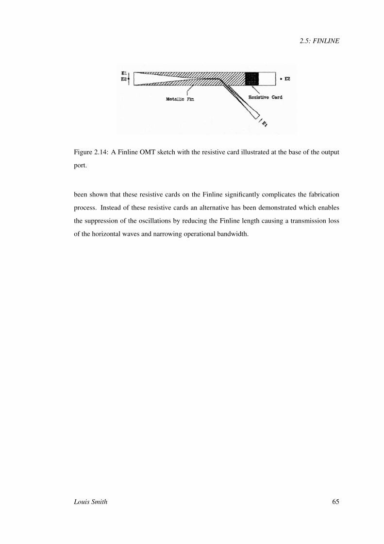
2.5: FINLINE
Figure 2.14: A Finline OMT sketch with the resistive card illustrated at the base of the output
port.
been shown that these resistive cards on the Finline significantly complicates the fabrication
process. Instead of these resistive cards an alternative has been demonstrated which enables
the suppression of the oscillations by reducing the Finline length causing a transmission loss
of the horizontal waves and narrowing operational bandwidth.
Louis Smith 65

2: CURRENT STATE OF OMT RESEARCH
66 Design and Feasibility Study of an Orthomode Transducer for the FAST Experiment
3
Detailed Development of a Turnstile
Junction, appropriate for the FAST
Experiment
3.1 The Turnstile Junction Waveguide OMT
A waveguide-based OMT is preferable for our application due to its compacted size and ability
to be linked to the wider waveguide based component, such as in this case a feed horn. It has
been decided that the small diameter and high complexity in respect to assembly of a compen-
sation pin or septum based system poses a significant challenge for a reliable and cost-effective
production of this device as if a class two method were to be chosen, especially during the
scale model feasibility stage. For this reason, as well as the reduced bandwidth experienced
due to it slight asymmetry results, this procedure has being discounted. An alternative to the
Boifot OMT as previously stated shall be used in this design, a class three turnstile junction as
described by Meyer and Goldberg in 1955. [33]
This configuration has been chosen due to its high performance characteristics in respect to
return losses and isolation especially across a relatively broad bandwidth as specified in the
performance requirements (this required broadband nature not being achievable using an asym-
metric class one or planar microstrip design). A full waveguide configuration also reduces the
Louis Smith 67
3: DETAILED DEVELOPMENT OF A TURNSTILE JUNCTION, APPROPRIATE FOR THEFAST EXPERIMENT
required complexity of this design in comparison to a hybrid form and thus alleviates manufac-
turability problems associated with the positioning and effective transfer between the varying
technologies i.e. the position and length of a coaxial probe within a waveguide turnstile junc-
tion.
A brief description of the various constituent parts required to produce an OMT based on a
turnstile junction network follows. We start with the characterisation of the turnstile junction
itself.
3.1.1 The Turnstile Splitting Junction
As previously mentioned the turnstile junction is a five-port microwave network connecting a
circular or square input port and four single mode rectangular waveguide outputs so providing
separation of the two input polarisations. The turnstile junction is an inherently broadband
component with excellent isolation and return losses. First developed by R. Dicke during the
second world war at the MIT Radiation Laboratory then expanded upon by Gehin and Tourneur
in 1986[34] into its modern wideband ridge-guide form. figure.3.1 shows the inherently three
dimensional structure of a turnstile junction with a metallic stub within the branching region.
68 Design and Feasibility Study of an Orthomode Transducer for the FAST Experiment
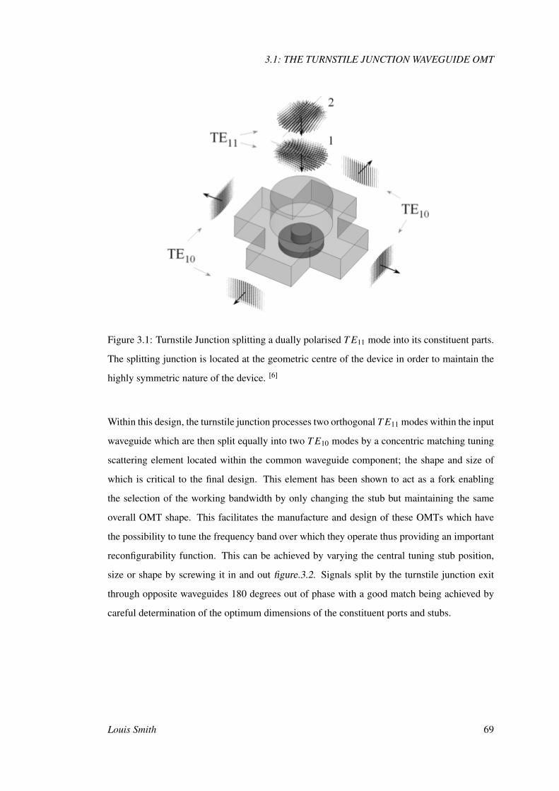
3.1: THE TURNSTILE JUNCTION WAVEGUIDE OMT
Figure 3.1: Turnstile Junction splitting a dually polarised T E11 mode into its constituent parts.
The splitting junction is located at the geometric centre of the device in order to maintain the
highly symmetric nature of the device. [6]
Within this design, the turnstile junction processes two orthogonal T E11 modes within the input
waveguide which are then split equally into two T E10 modes by a concentric matching tuning
scattering element located within the common waveguide component; the shape and size of
which is critical to the final design. This element has been shown to act as a fork enabling
the selection of the working bandwidth by only changing the stub but maintaining the same
overall OMT shape. This facilitates the manufacture and design of these OMTs which have
the possibility to tune the frequency band over which they operate thus providing an important
reconfigurability function. This can be achieved by varying the central tuning stub position,
size or shape by screwing it in and out figure.3.2. Signals split by the turnstile junction exit
through opposite waveguides 180 degrees out of phase with a good match being achieved by
careful determination of the optimum dimensions of the constituent ports and stubs.
Louis Smith 69
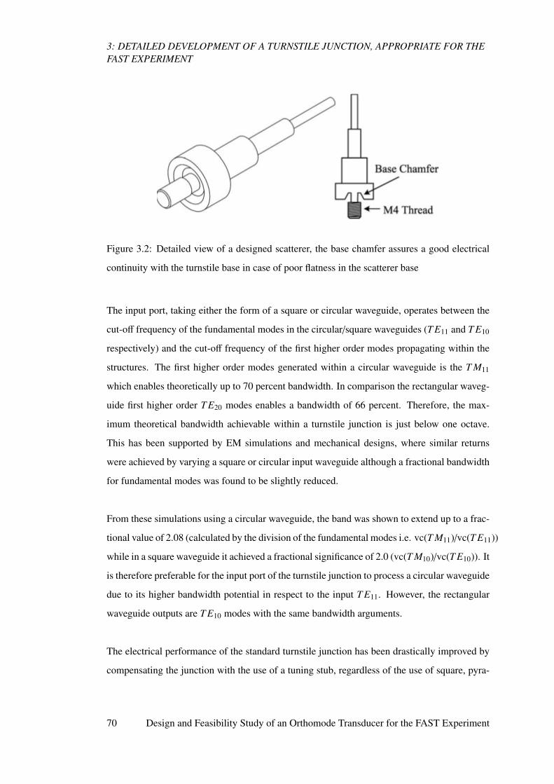
3: DETAILED DEVELOPMENT OF A TURNSTILE JUNCTION, APPROPRIATE FOR THEFAST EXPERIMENT
Figure 3.2: Detailed view of a designed scatterer, the base chamfer assures a good electrical
continuity with the turnstile base in case of poor flatness in the scatterer base
The input port, taking either the form of a square or circular waveguide, operates between the
cut-off frequency of the fundamental modes in the circular/square waveguides (T E11 and T E10
respectively) and the cut-off frequency of the first higher order modes propagating within the
structures. The first higher order modes generated within a circular waveguide is the T M11
which enables theoretically up to 70 percent bandwidth. In comparison the rectangular waveg-
uide first higher order T E20 modes enables a bandwidth of 66 percent. Therefore, the max-
imum theoretical bandwidth achievable within a turnstile junction is just below one octave.
This has been supported by EM simulations and mechanical designs, where similar returns
were achieved by varying a square or circular input waveguide although a fractional bandwidth
for fundamental modes was found to be slightly reduced.
From these simulations using a circular waveguide, the band was shown to extend up to a frac-
tional value of 2.08 (calculated by the division of the fundamental modes i.e. vc(T M11)/vc(T E11))
while in a square waveguide it achieved a fractional significance of 2.0 (vc(T M10)/vc(T E10)). It
is therefore preferable for the input port of the turnstile junction to process a circular waveguide
due to its higher bandwidth potential in respect to the input T E11. However, the rectangular
waveguide outputs are T E10 modes with the same bandwidth arguments.
The electrical performance of the standard turnstile junction has been drastically improved by
compensating the junction with the use of a tuning stub, regardless of the use of square, pyra-
70 Design and Feasibility Study of an Orthomode Transducer for the FAST Experiment
3.1: THE TURNSTILE JUNCTION WAVEGUIDE OMT
midal, multi-stepped cylindrical or other imaginative scattering elements as described in the
previous chapter. The use of effective EM computational tools has resulted in the quality of
this waveguide component being dramatically improved. As previously affirmed a recent pref-
erence for a two, three or four stub waveguide scatter has been established, due to the higher
performance in terms of bandwidth in comparison to other more exotic designs.
3.1.2 Compact 90 degree Twist
Within assemblies of rectangular waveguides for microwave systems various components are
required for the purpose of joining the waveguides, one being a twist section which itself can
be sub-divided into either a fixed or rotary system. Traditionally 90 degree twists, created by
a smooth variation of the waveguide walls have been employed for this purpose however these
have become less frequently utilized due to their difficulty in manufacture and by their inherent
exaggerated proportions.
The most frequent in respect to employment is a fixed twist section consisting merely of a
twisted singular section of waveguide while a rotary approach has become atypical. As a
functional element, twists are used for the provision of progressing a plane polarised wave by
rotating an output branch which itself is orientated at a variant angle. The main requirement
of a waveguide twist is its ease of design and manufacture, its provision for minimal reflection
and its operation within any specified frequency band. A secondary requirement unique for this
general purpose is also its compact characteristics so as not to excessively affect the overall size
of the entire OMT component.
A stepped twist is formed by a number of adjoining sections of straight rectangular waveg-
uides, a configuration suited for both fixed and rotary twist sections. It comprises two or more
adjoining sections of straight rectangular waveguides which are twisted about their common
axis at one or more junction faces.
The idea of the step twist in rectangular waveguides was first proposed by J.C. Slater during
his work at the Radiation Laboratory as a by-product from a vertebra type flexible waveguide;
Louis Smith 71
3: DETAILED DEVELOPMENT OF A TURNSTILE JUNCTION, APPROPRIATE FOR THEFAST EXPERIMENT
made of a series of short interlocking sections. It was found that these sections could be twisted
at the flange to form a rotary twist joint with the space between faces being equivalent to the
vertebra i.e. a quarter wavelength to facilitate the cancellation of their reflection. Commonly a
fixed step twist is utilised due to its numerous advantages over a twisted waveguide including
but not limited to its shape being of a prescribed dimension without any deforming process
enabling a more sophisticated design to be compressed.
Therefore, if the bandwidth within a guide is relatively narrow then a tuned system can be
made through the use of quarter-wave spacing between the fixed twist faces, thus the design
is termed tuned. This is to distinguish from a wideband design in which such spacing is not
effective over the bandwidth that is to say that the frequency bandwidth is about 12 percent, or
the guide wavelength bandwidth is about 18 percent. Such spacings are advantageous, however
if these respective bandwidths are increased to within a 40 to 80 percent range this system can
become unsuitable.[35]
Recently there has been a development away from standard faced twists towards wideband
compensation steps. A wideband stepped twist utilizes the principle of enlarging the width of
the waveguide to compensate for the constriction at the twisted faces, this usually takes the
form of deforming the shape of the waveguide. This compensation is nearly independent of
frequency, as is adapted to several twist faces to give a total angle of 90 degrees.
It has been suggested that a multi-section wideband step with a bow-tie shaped cross section
represents the best orientation for a waveguide based twist. This bow-tie shape[36] as illustrated
in figure 3.3 removes the corners present within the steps which can suffer from high electric
field intensity while at the same time providing enough degrees of freedom to achieve excel-
lent performance such as stringent return losses, bandwidth or rotation angle while at all times
maintaining an extremely compact profile. It has been shown that a return loss in excess of
-30dB is achievable with a bandwidth of approximately 40 percent. This smooth helix bow-tie
structure has however proven difficult to manufacture especially in conjunction with certain
manufacturing techniques.
72 Design and Feasibility Study of an Orthomode Transducer for the FAST Experiment
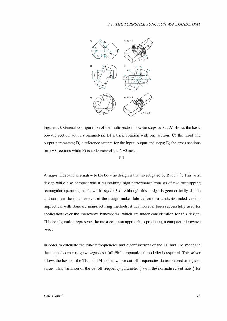
3.1: THE TURNSTILE JUNCTION WAVEGUIDE OMT
Figure 3.3: General configuration of the multi-section bow-tie steps twist : A) shows the basic
bow-tie section with its parameters; B) a basic rotation with one section; C) the input and
output parameters; D) a reference system for the input, output and steps; E) the cross sections
for n=3 sections while F) is a 3D view of the N=3 case.[36]
A major wideband alternative to the bow-tie design is that investigated by Rudd [37]. This twist
design while also compact whilst maintaining high performance consists of two overlapping
rectangular apertures, as shown in figure 3.4. Although this design is geometrically simple
and compact the inner corners of the design makes fabrication of a terahertz scaled version
impractical with standard manufacturing methods, it has however been successfully used for
applications over the microwave bandwidths, which are under consideration for this design.
This configuration represents the most common approach to producing a compact microwave
twist.
In order to calculate the cut-off frequencies and eigenfunctions of the TE and TM modes in
the stepped corner ridge waveguides a full EM computational modeller is required. This solver
allows the basis of the TE and TM modes whose cut-off frequencies do not exceed at a given
value. This variation of the cut-off frequency parameter aλ with the normalised cut size s
a for
Louis Smith 73
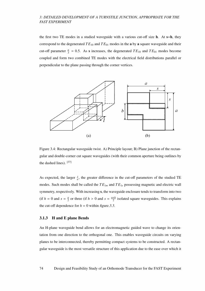
3: DETAILED DEVELOPMENT OF A TURNSTILE JUNCTION, APPROPRIATE FOR THEFAST EXPERIMENT
the first two TE modes in a studied waveguide with a various cut-off size h. At s=h, they
correspond to the degenerated T E10 and T E01 modes in the a by a square waveguide and their
cut-off parameter aλ = 0.5. As s increases, the degenerated T E10 and T E01 modes become
coupled and form two combined TE modes with the electrical field distributions parallel or
perpendicular to the plane passing through the corner vertices.
Figure 3.4: Rectangular waveguide twist. A) Principle layout; B) Plane junction of the rectan-
gular and double-corner cut square waveguides (with their common aperture being outlines by
the dashed lines). [37]
As expected, the larger sa , the greater difference in the cut-off parameters of the studied TE
modes. Such modes shall be called the T E1m and T E1e possessing magnetic and electric wall
symmetry, respectively. With increasing s, the waveguide enclosure tends to transform into two
(if h = 0 and s = a2 or three (if h > 0 and s = a+h
2 isolated square waveguides. This explains
the cut-off dependence for h = 0 within figure.3.3.
3.1.3 H and E plane Bends
An H-plane waveguide bend allows for an electromagnetic guided wave to change its orien-
tation from one direction to the orthogonal one. This enables waveguide circuits on varying
planes to be interconnected, thereby permitting compact systems to be constructed. A rectan-
gular waveguide is the most versatile structure of this application due to the ease over which it
74 Design and Feasibility Study of an Orthomode Transducer for the FAST Experiment
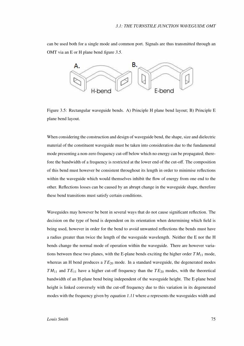
3.1: THE TURNSTILE JUNCTION WAVEGUIDE OMT
can be used both for a single mode and common port. Signals are thus transmitted through an
OMT via an E or H plane bend figure 3.5.
Figure 3.5: Rectangular waveguide bends. A) Principle H plane bend layout; B) Principle E
plane bend layout.
When considering the construction and design of waveguide bend, the shape, size and dielectric
material of the constituent waveguide must be taken into consideration due to the fundamental
mode presenting a non-zero frequency cut-off below which no energy can be propagated; there-
fore the bandwidth of a frequency is restricted at the lower end of the cut-off. The composition
of this bend must however be consistent throughout its length in order to minimise reflections
within the waveguide which would themselves inhibit the flow of energy from one end to the
other. Reflections losses can be caused by an abrupt change in the waveguide shape, therefore
these bend transitions must satisfy certain conditions.
Waveguides may however be bent in several ways that do not cause significant reflection. The
decision on the type of bend is dependent on its orientation when determining which field is
being used, however in order for the bend to avoid unwanted reflections the bends must have
a radius greater than twice the length of the waveguide wavelength. Neither the E nor the H
bends change the normal mode of operation within the waveguide. There are however varia-
tions between these two planes, with the E-plane bends exciting the higher order T M11 mode,
whereas an H bend produces a T E20 mode. In a standard waveguide, the degenerated modes
T M11 and T E11 have a higher cut-off frequency than the T E20 modes, with the theoretical
bandwidth of an H-plane bend being independent of the waveguide height. The E-plane bend
height is linked conversely with the cut-off frequency due to this variation in its degenerated
modes with the frequency given by equation 1.11 where a represents the waveguides width and
Louis Smith 75
3: DETAILED DEVELOPMENT OF A TURNSTILE JUNCTION, APPROPRIATE FOR THEFAST EXPERIMENT
b represents its height. The usable bandwidth for both types of bends is smaller than that of an
equivalent straight section of waveguide.
fcT E11
fcT E10=√
1 +ab
2(3.1)
It can be seen with the aid of equation 3.1 that by using an E-plane bend rather than a waveg-
uide H bend a wider bandwidth with a minimum of complexity can be achieved for balanced
phase operation. Additionally, since the cut off frequency for the T M11 is higher for reduced
height waveguide (a=4b), a further improvement in terms of matching has been reported to
have been achieved by reducing the waveguide height. The only limitation to this height re-
duction is in the manufacturability and in the theoretically increase in losses; for this reason
the use of reduced height waveguides was investigated for this application to ensure that the
design was practical and provided minimal return losses.
3.1.4 Y Junction Tapered Power Combiner
Y junctions are useful as power dividers or combiners in situations in which the more complex
four port 180 degree hybrid (magic T) is not required. This device can be used to combine the
two signals produced by a turnstile junction that requires also an additional 180 degree phase
shift between them. This is illustrated in figure 3.6 where pol.1 and pol.2 represent the two
input ports and pol.3 the output port. This device has been highly investigated by Kerr in [38],
whose HFSS simulations indicated that a return loss value above -35dB is readily achievable.
The bend for this device follows the same basic theory as that prescribed in the E-plane bend
as in section 1.2 and follows on from the less symmetric T based system which is unsuitable
for the blanket use of the FAST OMT due to its geometry being incompatible with the chosen
design.
In order to reduce the volume and maximise the broadband nature of this junction, the number
of tapers within this junction (which are akin to a Chebyshev Transformer) can be altered, as
well as their individual lengths, widths and spacings. It has been reported than an increase in
the frequency of branches within the body of the combiner (a minimum of two being required
76 Design and Feasibility Study of an Orthomode Transducer for the FAST Experiment
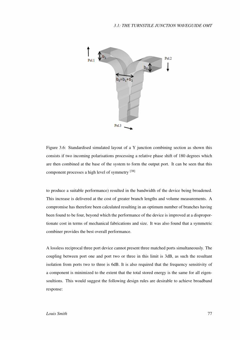
3.1: THE TURNSTILE JUNCTION WAVEGUIDE OMT
Figure 3.6: Standardised simulated layout of a Y junction combining section as shown this
consists if two incoming polarisations processing a relative phase shift of 180 degrees which
are then combined at the base of the system to form the output port. It can be seen that this
component processes a high level of symmetry [38]
to produce a suitable performance) resulted in the bandwidth of the device being broadened.
This increase is delivered at the cost of greater branch lengths and volume measurements. A
compromise has therefore been calculated resulting in an optimum number of branches having
been found to be four, beyond which the performance of the device is improved at a dispropor-
tionate cost in terms of mechanical fabrications and size. It was also found that a symmetric
combiner provides the best overall performance.
A lossless reciprocal three port device cannot present three matched ports simultaneously. The
coupling between port one and port two or three in this limit is 3dB, as such the resultant
isolation from ports two to three is 6dB. It is also required that the frequency sensitivity of
a component is minimized to the extent that the total stored energy is the same for all eigen-
soultions. This would suggest the following design rules are desirable to achieve broadband
response:
Louis Smith 77

3: DETAILED DEVELOPMENT OF A TURNSTILE JUNCTION, APPROPRIATE FOR THEFAST EXPERIMENT
1. The dominant mode symmetry should be preserved by junction geometry.
2. The guide heights of the three ports are linked by the power division ratio, R =b1b2
where all variables can be seen in figure.3.6.
3. A desire to minimise the frequency dependence of the junction discontinuities so as
such b0 = b1 + b2.
78 Design and Feasibility Study of an Orthomode Transducer for the FAST Experiment

Part II
Design and Results
Louis Smith 79

80 Design and Feasibility Study of an Orthomode Transducer for the FAST Experiment
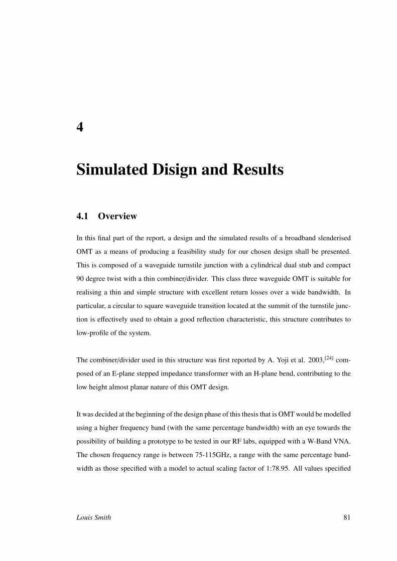
4
Simulated Disign and Results
4.1 Overview
In this final part of the report, a design and the simulated results of a broadband slenderised
OMT as a means of producing a feasibility study for our chosen design shall be presented.
This is composed of a waveguide turnstile junction with a cylindrical dual stub and compact
90 degree twist with a thin combiner/divider. This class three waveguide OMT is suitable for
realising a thin and simple structure with excellent return losses over a wide bandwidth. In
particular, a circular to square waveguide transition located at the summit of the turnstile junc-
tion is effectively used to obtain a good reflection characteristic, this structure contributes to
low-profile of the system.
The combiner/divider used in this structure was first reported by A. Yoji et al. 2003,[24] com-
posed of an E-plane stepped impedance transformer with an H-plane bend, contributing to the
low height almost planar nature of this OMT design.
It was decided at the beginning of the design phase of this thesis that is OMT would be modelled
using a higher frequency band (with the same percentage bandwidth) with an eye towards the
possibility of building a prototype to be tested in our RF labs, equipped with a W-Band VNA.
The chosen frequency range is between 75-115GHz, a range with the same percentage band-
width as those specified with a model to actual scaling factor of 1:78.95. All values specified
Louis Smith 81
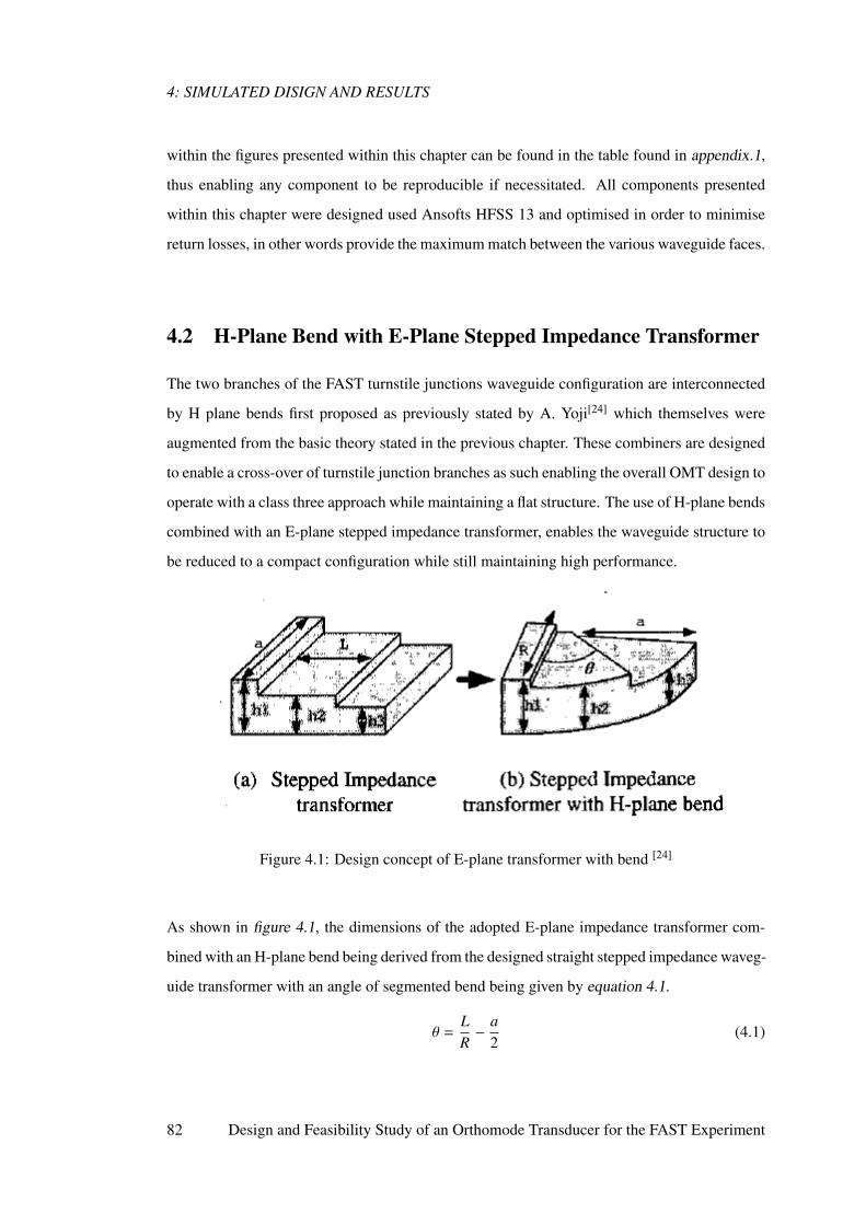
4: SIMULATED DISIGN AND RESULTS
within the figures presented within this chapter can be found in the table found in appendix.1,
thus enabling any component to be reproducible if necessitated. All components presented
within this chapter were designed used Ansofts HFSS 13 and optimised in order to minimise
return losses, in other words provide the maximum match between the various waveguide faces.
4.2 H-Plane Bend with E-Plane Stepped Impedance Transformer
The two branches of the FAST turnstile junctions waveguide configuration are interconnected
by H plane bends first proposed as previously stated by A. Yoji[24] which themselves were
augmented from the basic theory stated in the previous chapter. These combiners are designed
to enable a cross-over of turnstile junction branches as such enabling the overall OMT design to
operate with a class three approach while maintaining a flat structure. The use of H-plane bends
combined with an E-plane stepped impedance transformer, enables the waveguide structure to
be reduced to a compact configuration while still maintaining high performance.
Figure 4.1: Design concept of E-plane transformer with bend [24]
As shown in figure 4.1, the dimensions of the adopted E-plane impedance transformer com-
bined with an H-plane bend being derived from the designed straight stepped impedance waveg-
uide transformer with an angle of segmented bend being given by equation 4.1.
θ =LR−
a2
(4.1)
82 Design and Feasibility Study of an Orthomode Transducer for the FAST Experiment
4.2: H-PLANE BEND WITH E-PLANE STEPPED IMPEDANCE TRANSFORMER
This design was then produced and optimised using the commercial finite element analysis pro-
gram HFSS 13 with the resultant design being shown in figure 4.2. The various stepped height
parameters defined as the h variants in figure 4.1 were determined through the use of an opti-
misation program inbuilt into Ansofts HFSS package which enabled a value to be formulated
within a pre determined range set by the user.
Figure 4.2: Simulated 90 degree H-bend with an E-plane transition, as can be seen in A) and B)
the designed bend consists of five sections each of varying heights however processing the same
angle of transition from one to another (30 degrees). H1 and H5 represent the initial height of
a standard waveguide for this frequency band of 2.54mm while H5 has a relative height of
0.45H1 or 1.245mm, thus enabling the two OMT branches to pass over one another. As seen
in section C) the wave passes consistently through the bend without significant reflections
Figure.4.2 indicates the final designed H-bend design as seen on by the CAD program HFSS,
this device those similar to that first proposed by A.Yoji, however as can be seen in figure
4.3 significant improvements have been made in the defined return loss characteristics in com-
parison to those first proposed in the 2005 paper stemming from numerous varying step ratio
Louis Smith 83

4: SIMULATED DISIGN AND RESULTS
experiments having been conducted to ascertain the optimum orientation for this device. It was
found that a constant thirty degree variant between the three angled sub-sections resulted in
the most advantageous conclusions, it was also decided that in order for the two branches to
overlap with a suitable gap, a height reduction was set to 40 percent of the initial: from a full
height of (1.3mm) to reduced height (0.637mm).
As can be seen in figure 4.3 this H-plane bend represents a high-quality solution for a full to
reduced height H-bend. The return loss is below -25dB over a 80 percent bandwidth. The
average return is -32dB. Better performance is achieved in the middle of the band whereas
values up to -18dB are achieved at the edge of the band.
84 Design and Feasibility Study of an Orthomode Transducer for the FAST Experiment
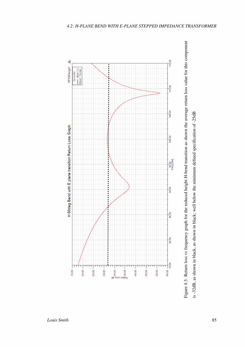
4.2: H-PLANE BEND WITH E-PLANE STEPPED IMPEDANCE TRANSFORMER
Figu
re4.
3:R
etur
nlo
ssvs
freq
uenc
ygr
aph
fort
here
duce
dhe
ight
H-b
end
tran
sitio
nas
show
nth
eav
erag
ere
turn
loss
valu
efo
rthi
sco
mpo
nent
is-3
2dB
,as
show
nin
blac
k,as
show
nin
blac
k;w
ellb
elow
the
min
imum
defin
edsp
ecifi
catio
nof
-25d
B
Louis Smith 85
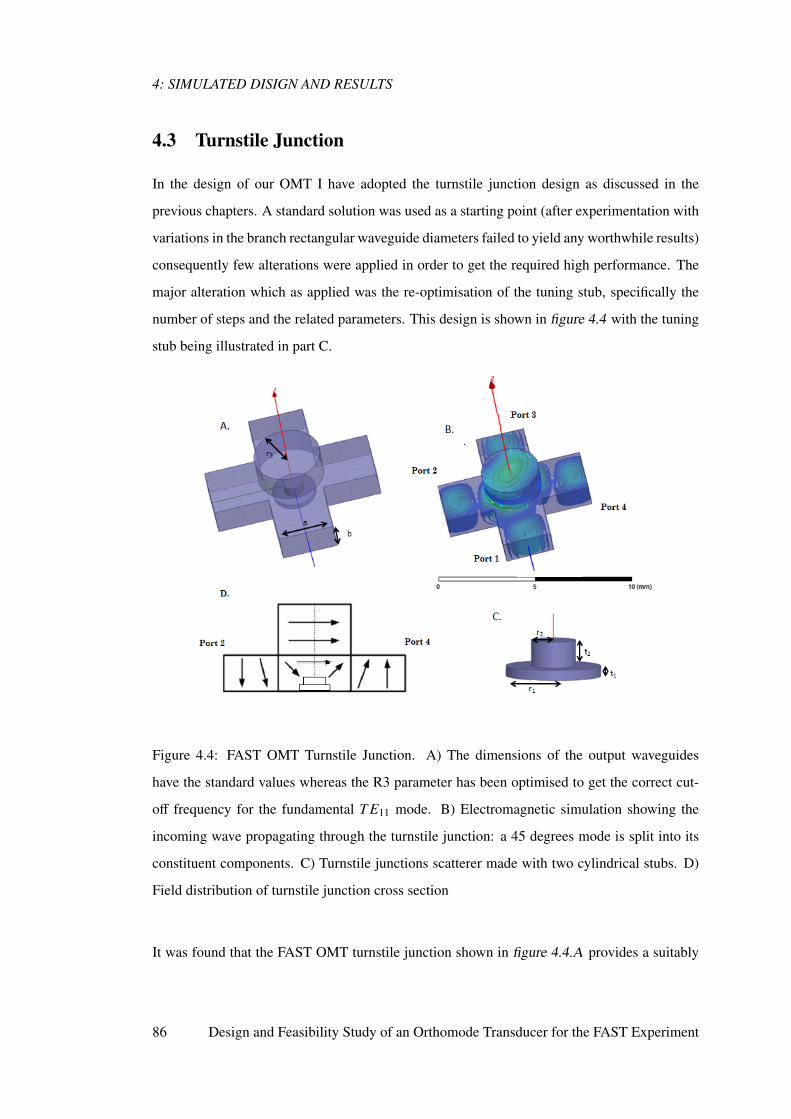
4: SIMULATED DISIGN AND RESULTS
4.3 Turnstile Junction
In the design of our OMT I have adopted the turnstile junction design as discussed in the
previous chapters. A standard solution was used as a starting point (after experimentation with
variations in the branch rectangular waveguide diameters failed to yield any worthwhile results)
consequently few alterations were applied in order to get the required high performance. The
major alteration which as applied was the re-optimisation of the tuning stub, specifically the
number of steps and the related parameters. This design is shown in figure 4.4 with the tuning
stub being illustrated in part C.
Figure 4.4: FAST OMT Turnstile Junction. A) The dimensions of the output waveguides
have the standard values whereas the R3 parameter has been optimised to get the correct cut-
off frequency for the fundamental T E11 mode. B) Electromagnetic simulation showing the
incoming wave propagating through the turnstile junction: a 45 degrees mode is split into its
constituent components. C) Turnstile junctions scatterer made with two cylindrical stubs. D)
Field distribution of turnstile junction cross section
It was found that the FAST OMT turnstile junction shown in figure 4.4.A provides a suitably
86 Design and Feasibility Study of an Orthomode Transducer for the FAST Experiment
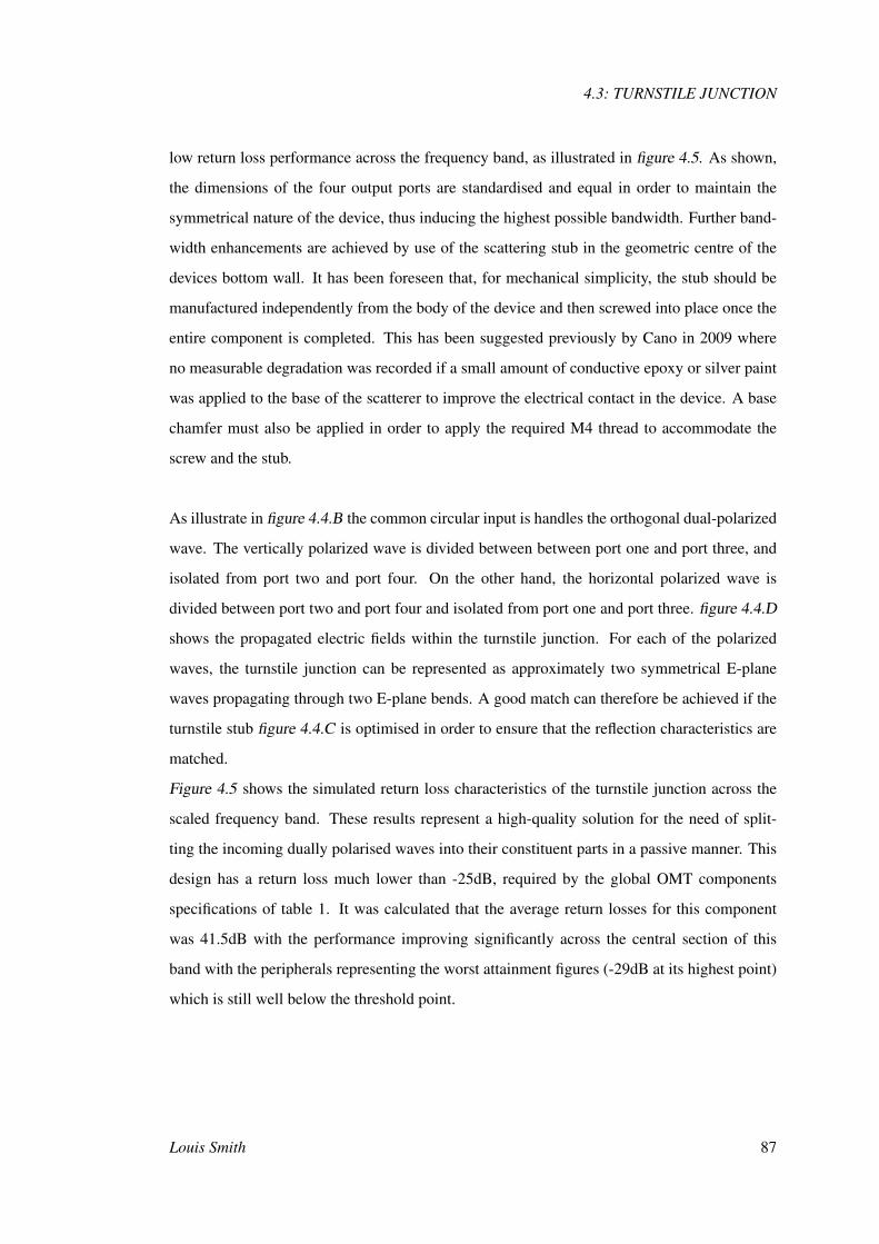
4.3: TURNSTILE JUNCTION
low return loss performance across the frequency band, as illustrated in figure 4.5. As shown,
the dimensions of the four output ports are standardised and equal in order to maintain the
symmetrical nature of the device, thus inducing the highest possible bandwidth. Further band-
width enhancements are achieved by use of the scattering stub in the geometric centre of the
devices bottom wall. It has been foreseen that, for mechanical simplicity, the stub should be
manufactured independently from the body of the device and then screwed into place once the
entire component is completed. This has been suggested previously by Cano in 2009 where
no measurable degradation was recorded if a small amount of conductive epoxy or silver paint
was applied to the base of the scatterer to improve the electrical contact in the device. A base
chamfer must also be applied in order to apply the required M4 thread to accommodate the
screw and the stub.
As illustrate in figure 4.4.B the common circular input is handles the orthogonal dual-polarized
wave. The vertically polarized wave is divided between between port one and port three, and
isolated from port two and port four. On the other hand, the horizontal polarized wave is
divided between port two and port four and isolated from port one and port three. figure 4.4.D
shows the propagated electric fields within the turnstile junction. For each of the polarized
waves, the turnstile junction can be represented as approximately two symmetrical E-plane
waves propagating through two E-plane bends. A good match can therefore be achieved if the
turnstile stub figure 4.4.C is optimised in order to ensure that the reflection characteristics are
matched.
Figure 4.5 shows the simulated return loss characteristics of the turnstile junction across the
scaled frequency band. These results represent a high-quality solution for the need of split-
ting the incoming dually polarised waves into their constituent parts in a passive manner. This
design has a return loss much lower than -25dB, required by the global OMT components
specifications of table 1. It was calculated that the average return losses for this component
was 41.5dB with the performance improving significantly across the central section of this
band with the peripherals representing the worst attainment figures (-29dB at its highest point)
which is still well below the threshold point.
Louis Smith 87
4: SIMULATED DISIGN AND RESULTS
Figu
re4.
5:Si
mul
ated
retu
rnlo
ssch
arac
teri
stic
sfo
rthe
inde
pend
entT
urns
tile
Junc
tion
acro
ssth
ech
osen
scal
edfr
eque
ncy
band
,itc
anbe
seen
that
the
aver
age
retu
rnlo
ssfo
rthi
sco
mpo
nent
was
-41d
B.
88 Design and Feasibility Study of an Orthomode Transducer for the FAST Experiment
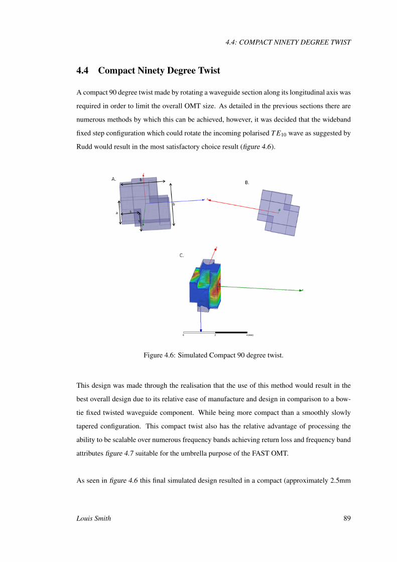
4.4: COMPACT NINETY DEGREE TWIST
4.4 Compact Ninety Degree Twist
A compact 90 degree twist made by rotating a waveguide section along its longitudinal axis was
required in order to limit the overall OMT size. As detailed in the previous sections there are
numerous methods by which this can be achieved, however, it was decided that the wideband
fixed step configuration which could rotate the incoming polarised T E10 wave as suggested by
Rudd would result in the most satisfactory choice result (figure 4.6).
Figure 4.6: Simulated Compact 90 degree twist.
This design was made through the realisation that the use of this method would result in the
best overall design due to its relative ease of manufacture and design in comparison to a bow-
tie fixed twisted waveguide component. While being more compact than a smoothly slowly
tapered configuration. This compact twist also has the relative advantage of processing the
ability to be scalable over numerous frequency bands achieving return loss and frequency band
attributes figure 4.7 suitable for the umbrella purpose of the FAST OMT.
As seen in figure 4.6 this final simulated design resulted in a compact (approximately 2.5mm
Louis Smith 89
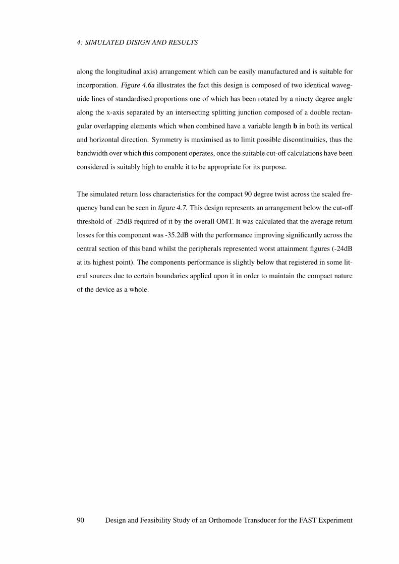
4: SIMULATED DISIGN AND RESULTS
along the longitudinal axis) arrangement which can be easily manufactured and is suitable for
incorporation. Figure 4.6a illustrates the fact this design is composed of two identical waveg-
uide lines of standardised proportions one of which has been rotated by a ninety degree angle
along the x-axis separated by an intersecting splitting junction composed of a double rectan-
gular overlapping elements which when combined have a variable length b in both its vertical
and horizontal direction. Symmetry is maximised as to limit possible discontinuities, thus the
bandwidth over which this component operates, once the suitable cut-off calculations have been
considered is suitably high to enable it to be appropriate for its purpose.
The simulated return loss characteristics for the compact 90 degree twist across the scaled fre-
quency band can be seen in figure 4.7. This design represents an arrangement below the cut-off
threshold of -25dB required of it by the overall OMT. It was calculated that the average return
losses for this component was -35.2dB with the performance improving significantly across the
central section of this band whilst the peripherals represented worst attainment figures (-24dB
at its highest point). The components performance is slightly below that registered in some lit-
eral sources due to certain boundaries applied upon it in order to maintain the compact nature
of the device as a whole.
90 Design and Feasibility Study of an Orthomode Transducer for the FAST Experiment
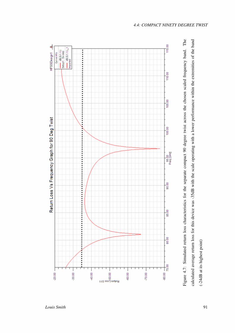
4.4: COMPACT NINETY DEGREE TWIST
Figu
re4.
7:Si
mul
ated
retu
rnlo
ssch
arac
teri
stic
sfo
rth
ese
para
teco
mpa
ct90
degr
eetw
ist
acro
ssth
ech
osen
scal
edfr
eque
ncy
band
.T
he
calc
ulat
edav
erag
ere
turn
loss
for
this
devi
cew
as-3
5dB
with
the
scal
eop
erat
ing
with
alo
wer
perf
orm
ance
with
inth
eex
trem
ities
ofth
eba
nd
(-24
dBat
itshi
ghes
tpoi
nt)
Louis Smith 91
4: SIMULATED DISIGN AND RESULTS
4.5 Y Junction Tapered Power Combiner
For the purpose of combining the two constituent input waves, each of which experiencing a
relative phase shift of 180 degrees into a singular output port a Y-junction tapered power com-
biner was elected; similar to those by Kerr in 2001 and detaled in the preceding literature. As
previously stated in order to reduce the length and amplify the broadband nature of this device
a tapering system was employed in which both the length and width of each individual section
was determined with the preliminary values chosen in accordance with binomial rules then op-
timised using HFSS. This optimisation was also conducted in respect to the other variables as
illustrated in figure 4.8, with the matching resulting in said design.
It was found that an atypical arrangement of four independent tappers resulted in a suitable
compromise between a satisfactory selection of measurements in respect to the overall FAST
requirements whilst still maintaining its manufacturable which could be enhanced by a reduc-
tion in said graduation, however at an unsuitable cost to performance.
Figure 4.8: Simulated Y junctions. Sections A) and B) in this figure comprises the final HFSS
design as described in the previous literature as seen this processes similarities to those first
proposed by Kerr with the input and output waveguides having been given the standardised
universal dimensions present throughout the entire design.
92 Design and Feasibility Study of an Orthomode Transducer for the FAST Experiment
4.5: Y JUNCTION TAPERED POWER COMBINER
As can be seen in figure 4.8 this structure was kept symmetrical along both the z and y planes
resulting in the broadest bandwidth possible while still maintaining a good return loss. In the
Kerr orientation, the two incoming full-height rectangular waveguide meet in square waveguide
sections which are then transformed back into rectangular waveguides. The resultant combiner
design is thus relatively long (approximately 8mm within the W-band). It was seen as vital
to maintain a minimum length for this section of the device as its presence in the final OMT
design represents a significant limitation in the final compactness of the design therefore a re-
duction of 25 percent was applied while some of the more mechanically challenging smooth
bends were replaced by a reductive step based system.
This design produced simulated return losses as displayed in figure 4.9 across the scaled fre-
quency band, it can be seen that the average return losses for this component was -34dB with
a range of between -30dB at the fringes to -45dB across the central region of the band. These
simulated measurements results in the component being deemed as suitable for the purpose for
which it was design as its characteristics were within the specifications for the FAST compo-
nent.
Louis Smith 93
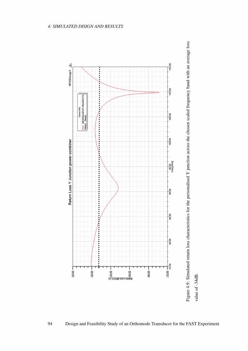
4: SIMULATED DISIGN AND RESULTS
Figu
re4.
9:Si
mul
ated
retu
rnlo
ssch
arac
teri
stic
sfo
rth
epe
rson
alis
edY
junc
tion
acro
ssth
ech
osen
scal
edfr
eque
ncy
band
with
anav
erag
elo
ss
valu
eof
-34d
B.
94 Design and Feasibility Study of an Orthomode Transducer for the FAST Experiment
4.6: SIMULATED FAST OMT DESIGN
4.6 Simulated FAST OMT Design
Once the various constituent sections of the OMT were identified and simulated to a suitably
high standard so as not to representing a potentially limiting factor. Each of these subcompo-
nents were then united to form a global model following a predetermined blueprint. Interac-
tions between the sub-components, i.e. mismatches and phase differences, were automatically
considered and rectified within a first order approximation by human intervention then fine-
tuned with the use of an optimisation function. An electrical conductivity of σ = 1.5x10⁷
mho/m was applied to compensate for surface roughness and discontinuities of the assumed
gold-plated external walls of the waveguides. This value was established from comparisons
taken from electroformed components to measurements of other WR10 systems, the scaled
wave on which this L-band component is based[6]. It was foreseen that this method shall be
used as the initial feasibility models method of production due to its superior results in at the
chosen frequency.
The structure of this OMT design could have taken numerous forms, with the main influencing
factors being the decision to produce a waveguide based transducer, with a high symmetry and
physically compact design being made paramount it was also decided that for ease of manufac-
turability and reproduction a closely planar approach was advantageous. This resultant OMT
design can be seen in figure 4.10 where the simulated H bend was used as a means of connect-
ing the outgoing turnstile junction branches with combining junction via the use of a reduced
height waveguide. This design facilitated the two branches to overlap one other within the
same general plain by means of flipping the orientation of the H bends in the z-direction thus
reducing the size of the overall design in comparison to similar formations. For this reason an
H-plane bend was seen as necessary as it alone facilitates this compact design to be achieved
in this manner.
This system of stepped impedance H bends has been applied previously in other waveguide
based OMTs were a component of high performance was achieved at a reduced size. The
unique nature of this device however lies with the use of a compact 90 degree twist, enabling
the OMT to operate over a generalised plane, thus facilitating a reduction in complexity of
Louis Smith 95
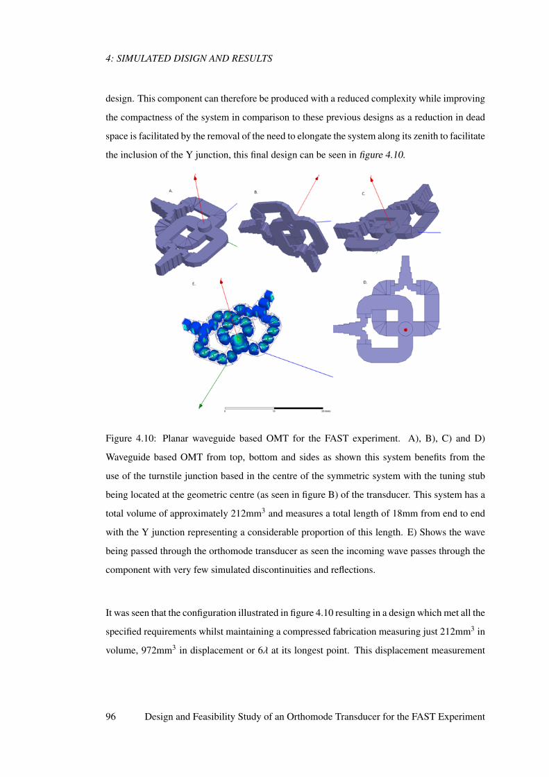
4: SIMULATED DISIGN AND RESULTS
design. This component can therefore be produced with a reduced complexity while improving
the compactness of the system in comparison to these previous designs as a reduction in dead
space is facilitated by the removal of the need to elongate the system along its zenith to facilitate
the inclusion of the Y junction, this final design can be seen in figure 4.10.
Figure 4.10: Planar waveguide based OMT for the FAST experiment. A), B), C) and D)
Waveguide based OMT from top, bottom and sides as shown this system benefits from the
use of the turnstile junction based in the centre of the symmetric system with the tuning stub
being located at the geometric centre (as seen in figure B) of the transducer. This system has a
total volume of approximately 212mm3 and measures a total length of 18mm from end to end
with the Y junction representing a considerable proportion of this length. E) Shows the wave
being passed through the orthomode transducer as seen the incoming wave passes through the
component with very few simulated discontinuities and reflections.
It was seen that the configuration illustrated in figure 4.10 resulting in a design which met all the
specified requirements whilst maintaining a compressed fabrication measuring just 212mm3 in
volume, 972mm3 in displacement or 6λ at its longest point. This displacement measurement
96 Design and Feasibility Study of an Orthomode Transducer for the FAST Experiment
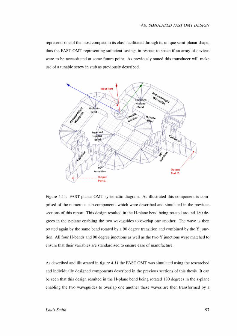
4.6: SIMULATED FAST OMT DESIGN
represents one of the most compact in its class facilitated through its unique semi-planar shape,
thus the FAST OMT representing sufficient savings in respect to space if an array of devices
were to be necessitated at some future point. As previously stated this transducer will make
use of a tunable screw in stub as previously described.
Figure 4.11: FAST planar OMT systematic diagram. As illustrated this component is com-
prised of the numerous sub-components which were described and simulated in the previous
sections of this report. This design resulted in the H-plane bend being rotated around 180 de-
grees in the z-plane enabling the two waveguides to overlap one another. The wave is then
rotated again by the same bend rotated by a 90 degree transition and combined by the Y junc-
tion. All four H-bends and 90 degree junctions as well as the two Y junctions were matched to
ensure that their variables are standardised to ensure ease of manufacture.
As described and illustrated in figure 4.11 the FAST OMT was simulated using the researched
and individually designed components described in the previous sections of this thesis. It can
be seen that this design resulted in the H-plane bend being rotated 180 degrees in the z-plane
enabling the two waveguides to overlap one another these waves are then transformed by a
Louis Smith 97
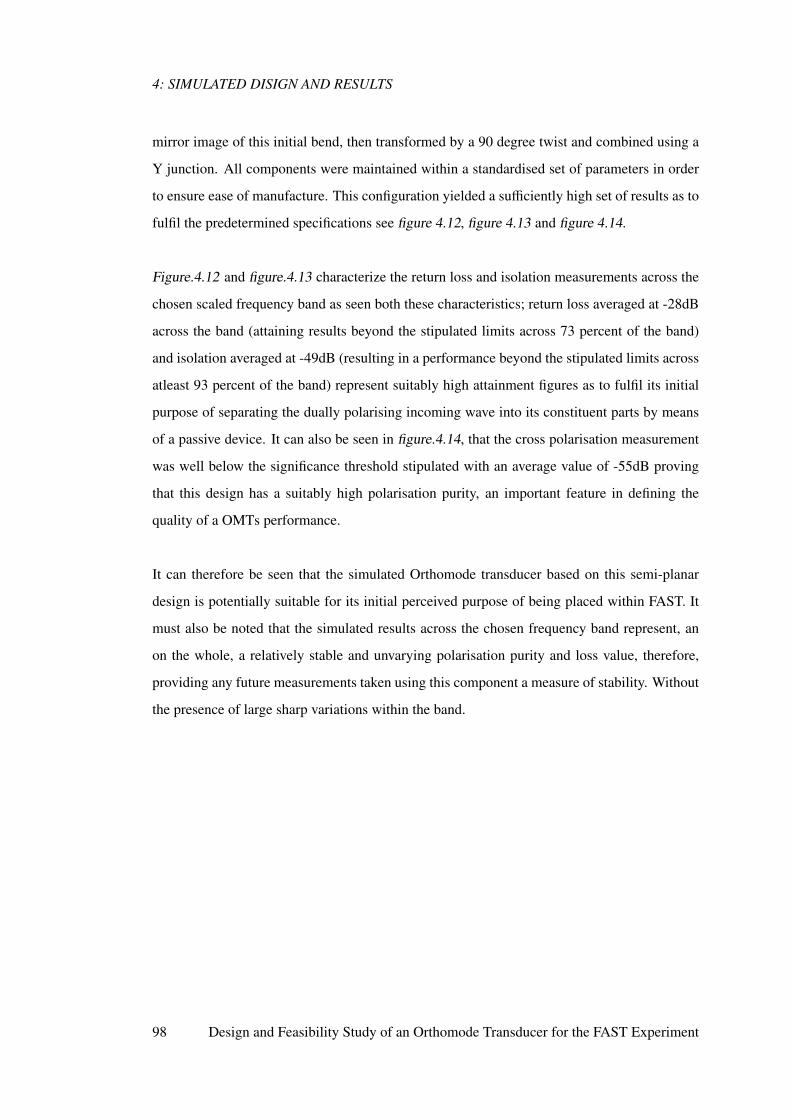
4: SIMULATED DISIGN AND RESULTS
mirror image of this initial bend, then transformed by a 90 degree twist and combined using a
Y junction. All components were maintained within a standardised set of parameters in order
to ensure ease of manufacture. This configuration yielded a sufficiently high set of results as to
fulfil the predetermined specifications see figure 4.12, figure 4.13 and figure 4.14.
Figure.4.12 and figure.4.13 characterize the return loss and isolation measurements across the
chosen scaled frequency band as seen both these characteristics; return loss averaged at -28dB
across the band (attaining results beyond the stipulated limits across 73 percent of the band)
and isolation averaged at -49dB (resulting in a performance beyond the stipulated limits across
atleast 93 percent of the band) represent suitably high attainment figures as to fulfil its initial
purpose of separating the dually polarising incoming wave into its constituent parts by means
of a passive device. It can also be seen in figure.4.14, that the cross polarisation measurement
was well below the significance threshold stipulated with an average value of -55dB proving
that this design has a suitably high polarisation purity, an important feature in defining the
quality of a OMTs performance.
It can therefore be seen that the simulated Orthomode transducer based on this semi-planar
design is potentially suitable for its initial perceived purpose of being placed within FAST. It
must also be noted that the simulated results across the chosen frequency band represent, an
on the whole, a relatively stable and unvarying polarisation purity and loss value, therefore,
providing any future measurements taken using this component a measure of stability. Without
the presence of large sharp variations within the band.
98 Design and Feasibility Study of an Orthomode Transducer for the FAST Experiment
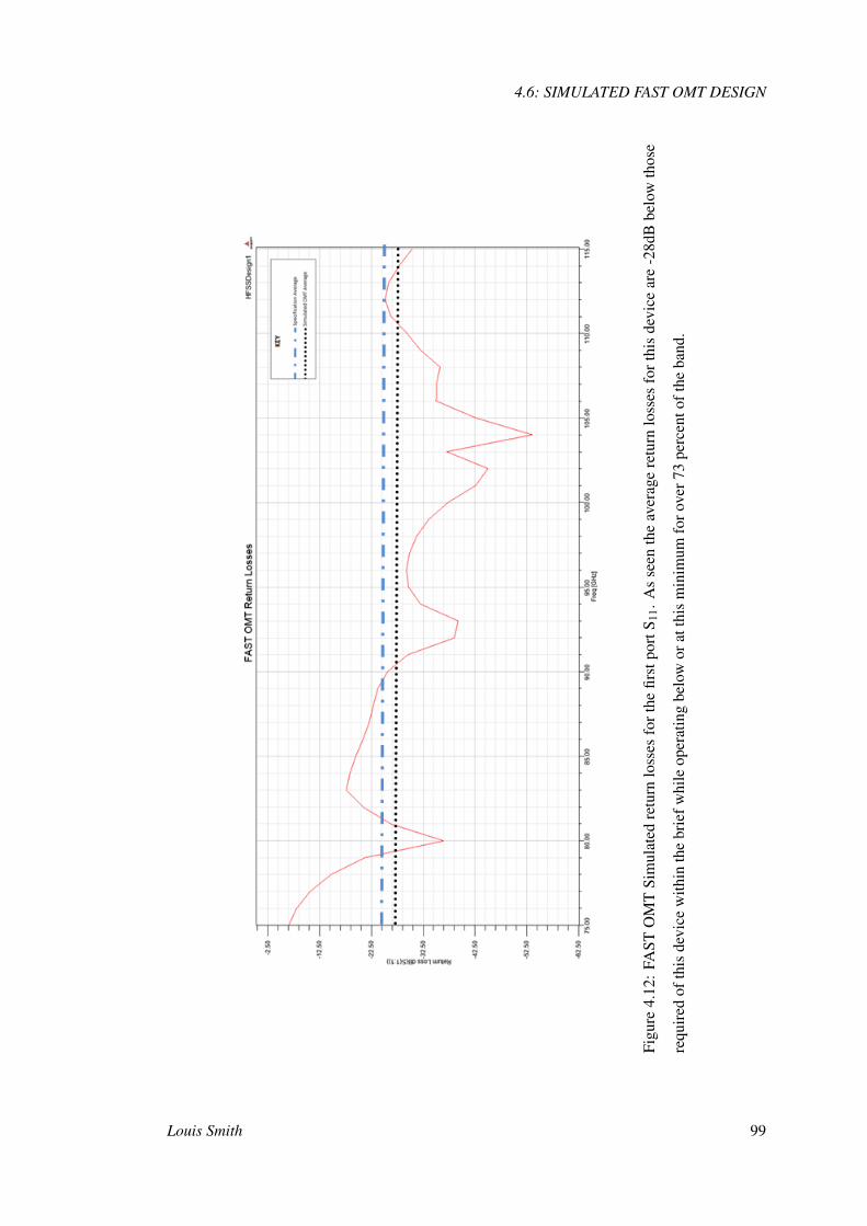
4.6: SIMULATED FAST OMT DESIGN
Figu
re4.
12:
FAST
OM
TSi
mul
ated
retu
rnlo
sses
fort
hefir
stpo
rtS 1
1.A
sse
enth
eav
erag
ere
turn
loss
esfo
rthi
sde
vice
are
-28d
Bbe
low
thos
e
requ
ired
ofth
isde
vice
with
inth
ebr
iefw
hile
oper
atin
gbe
low
orat
this
min
imum
foro
ver7
3pe
rcen
toft
heba
nd.
Louis Smith 99
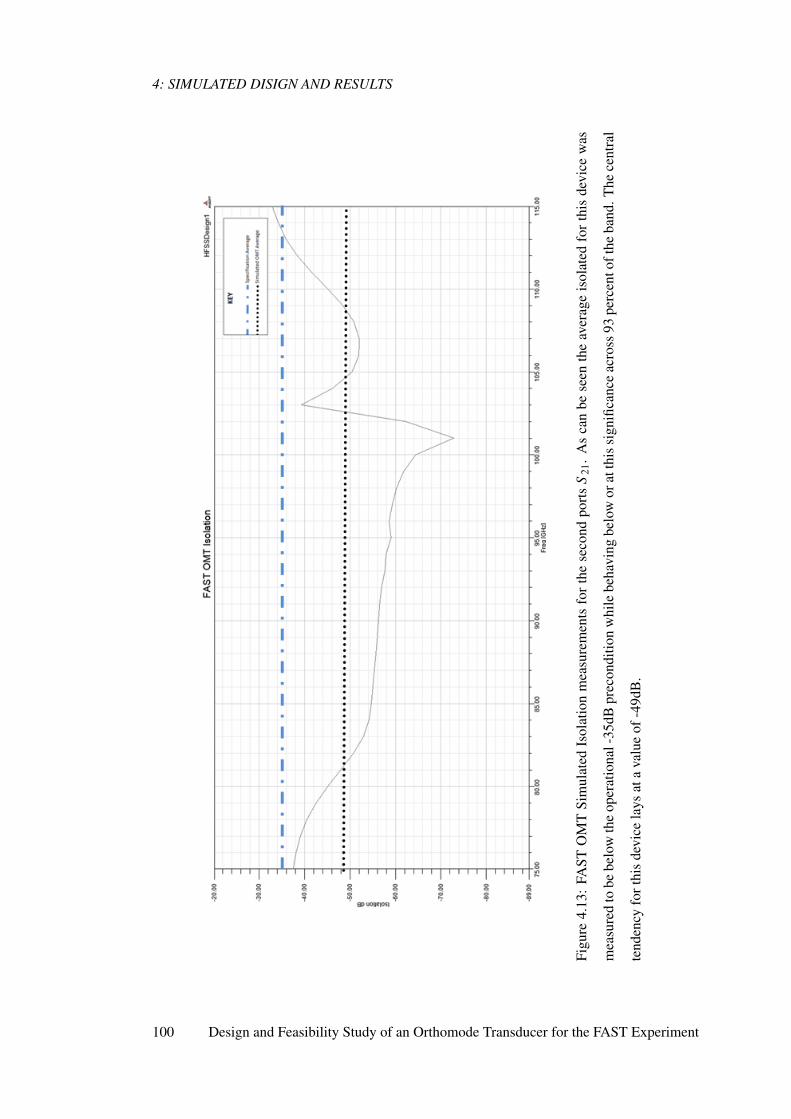
4: SIMULATED DISIGN AND RESULTS
Figu
re4.
13:
FAST
OM
TSi
mul
ated
Isol
atio
nm
easu
rem
ents
for
the
seco
ndpo
rts
S21
.A
sca
nbe
seen
the
aver
age
isol
ated
for
this
devi
cew
as
mea
sure
dto
bebe
low
the
oper
atio
nal-
35dB
prec
ondi
tion
whi
lebe
havi
ngbe
low
orat
this
sign
ifica
nce
acro
ss93
perc
ento
fthe
band
.The
cent
ral
tend
ency
fort
his
devi
cela
ysat
ava
lue
of-4
9dB
.
100 Design and Feasibility Study of an Orthomode Transducer for the FAST Experiment
4.6: SIMULATED FAST OMT DESIGN
Figu
re4.
14:
FAST
OM
TSi
mul
ated
Cro
ssPo
lari
satio
nm
easu
rem
ents
for
the
seco
ndpo
rts
S21
.A
sca
nbe
seen
the
aver
age
cros
spo
lari
satio
n
fort
his
devi
cew
asm
easu
red
tobe
belo
wth
eop
erat
iona
l-20
dBpr
econ
ditio
nw
ithan
aver
age
valu
ebe
ing
reco
rded
at-5
5.6d
B,t
here
fore
itca
n
bese
enth
isth
isde
vice
has
asu
itabl
yhi
ghpo
lari
satio
npu
rity
.
Louis Smith 101

4: SIMULATED DISIGN AND RESULTS
102 Design and Feasibility Study of an Orthomode Transducer for the FAST Experiment
5
Conclusions and Future Work
5.1 Conclusion
This report has demonstrated the feasibility, design and simulation of a waveguide based ortho-
mode transducer using a compact twist 90 degree module, turnstile junction splitter, H-plane
bend and Y junction power combiner. Various approaches were outlined as means of solving
the FAST requirement specification, however a final design based on a class three waveguide
turnstile junction approach was chosen due to its broadband high performance nature stemming
from its highly symmetric nature.
This final design is compact and is compatible with a circular input required to operate over
the 0.95−1.45GHz L-band however this latter simulated design was a scaled version operating
at a chosen higher frequency of 75−115GHz due to its ability to be assessed using the Manch-
ester Universities W-band VNA. This therefore enables the design to be manufactured using
electroforming techniques and assessed in its scaled form expanding the potential scope of
this feasibility report while instantly indicating the natural progression which the author feels
should be taken during the future work conducted towards proving the feasibility of this design.
The finally simulated scaled OMT has been extensively optimised to operate over a 35 percent
bandwidth centred at 90GHz, while maintaining an average return loss and isolation figure
in excess of those specified as the threshold values of -25dB and -35dB respectively. This
Louis Smith 103
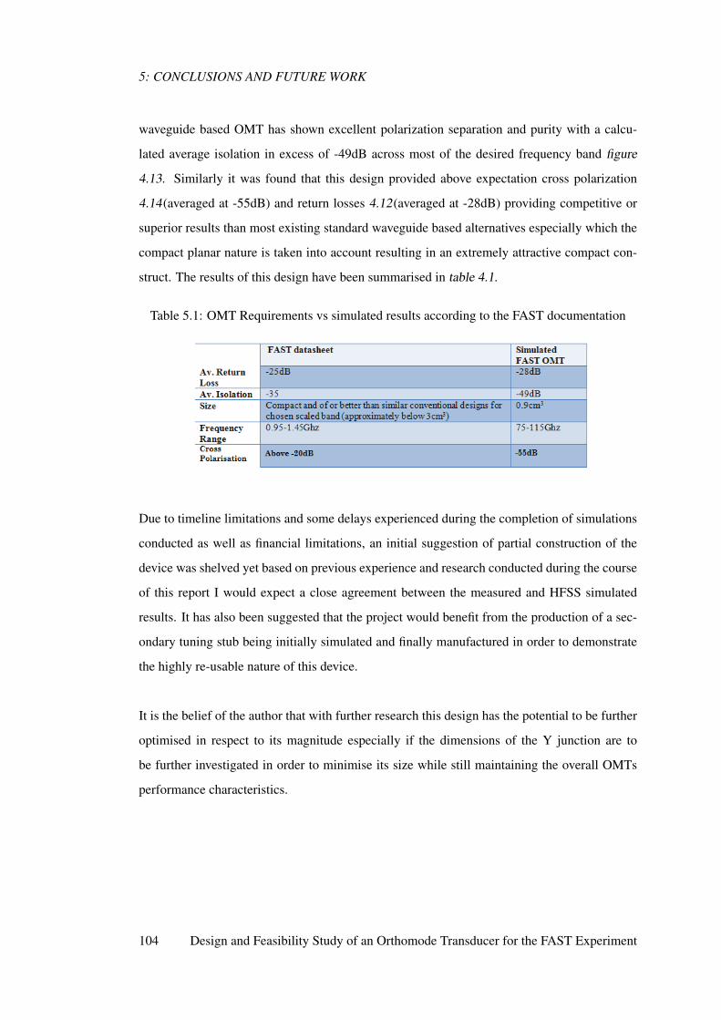
5: CONCLUSIONS AND FUTURE WORK
waveguide based OMT has shown excellent polarization separation and purity with a calcu-
lated average isolation in excess of -49dB across most of the desired frequency band figure
4.13. Similarly it was found that this design provided above expectation cross polarization
4.14(averaged at -55dB) and return losses 4.12(averaged at -28dB) providing competitive or
superior results than most existing standard waveguide based alternatives especially which the
compact planar nature is taken into account resulting in an extremely attractive compact con-
struct. The results of this design have been summarised in table 4.1.
Table 5.1: OMT Requirements vs simulated results according to the FAST documentation
Due to timeline limitations and some delays experienced during the completion of simulations
conducted as well as financial limitations, an initial suggestion of partial construction of the
device was shelved yet based on previous experience and research conducted during the course
of this report I would expect a close agreement between the measured and HFSS simulated
results. It has also been suggested that the project would benefit from the production of a sec-
ondary tuning stub being initially simulated and finally manufactured in order to demonstrate
the highly re-usable nature of this device.
It is the belief of the author that with further research this design has the potential to be further
optimised in respect to its magnitude especially if the dimensions of the Y junction are to
be further investigated in order to minimise its size while still maintaining the overall OMTs
performance characteristics.
104 Design and Feasibility Study of an Orthomode Transducer for the FAST Experiment

Part III
Appendices
Louis Smith 105

106 Design and Feasibility Study of an Orthomode Transducer for the FAST Experiment

References
[1] R. Nan, D. Li, C. Jin, Q. Wang, L. Zhu, W. Zhu, H. Zhang, Y. Yue & L. Qian. "The FIVE-Hundred-Meter Aperture
Spherical Radio Telescope (FAST) Project." International Journal of Modern Physics. 2006 pp:1-36.
[2] E.J. Wollack, W. Grammer and J.Kingsley. The Boifot Orthomode Junction. NRAO, ALMA Memo Series 425, 2002.
[3] E. Wollack. “A Full Waveguide Band Orthomode Junction.” NRAO, Charlottesville, May 1996.
[4] R. Garcia, F. Mayol, J.M. Montero and A. Culebras. “Circular Polarisation feed with Dual-Frequency OMT-Based
Turnstile Junction,” IEEE Antennas and Propagation Magazine, Vol. 53, No.1 Feb 2011.
[5] Robertson, S.D. “Recent Advances in Finline Circuits.” IRE Transactions on Microwave Theory and Techniques, Oct
1999: 263-267.
[6] G. Pisano, L. Pietranera, K. Isaak, L. Piccirillo, B. Johnson, B. Maffei & S. Melhuish. “A Broadband WR10 Turnstile
Junction Orthomode Transducer.” IEEE Microwave and Wireless Components Letters, Vol.17, No.4, April 2007:
286-288.
[7] Chang, Kai. “Orthomode Transducer.” In Encyclopedia of RF and Microwave Engineering Vol. 1-6, by R. Nesti, G.
Pelosi & S. Selleri G.G. Gentili, 3547-3563. John Wiley and Sons, 2005.
[8] E. J. Wollack, J. Gundersen, “Corrugated Platelet Feed Arrays for Millimeter-Wave Imaging,”, MB Polarization
Technology Workshop Presentation, 2010.
[9] A. I. Sandhu, “Design of an Orthomode Transducer in Gap Waveguide Technology,” Chambers Antenna Group,
Masters of Science Thesis in the program Communication Engineering. Septermber 2010
[10] M, Kamikura, M. Naruse, S. Asayama, N. Satou, W. Shan & Y. Sekimoto. “Development of a 385-500 GHz
Orthomode Transducer (OMT).” 19th Internation Symposium on Space Terahertz Technology. Groningen,
Neatherlands, April 2008. 557-562.
[11] Jackson, R. W. “A Planar Orthomode Transducer.” IEEE Microwave and Wireless Components Letters, Vol.11,
No.12, Dec 2001: 483-485.
[12] P.K. Grimes, O.G. King, G. Yassin & M.E. Jones. Compact broadband Planar Orthomode Transducer. Electronic
Letters,Vol,43, No.21, Oct 2007.
[13] A.M. Boifot, E. Lier & T. Schaug-Pettersen. “Simple and Broadband Orthomode Transducer.” IEE Proceedings, Vol.
137, No. 6,
[14] Erickson, G. Narayanan & N.R. “A Novel Full Waveguide Band Orthomode Transducer.” 13th International
Symposium on Space Terahertz Technology. Harvard, USA, March 2002. 505-514.
[15] A. Navarrini, C. Groppi & G. Chattopadhyay. “A Waveguide Orthomode Transducer for 385-500 GHz.” 21st
International Symposium on Space Terahertz Technology. Oxford, UK, March 2010. 328-337.
[16] A. Navarrini, R.L. Plambeck & D. Chow. “A Turnstile Junction Waveguide Orthomode Transducer for the 1mm
Band.” 19th International Symposium on Space Terahertz Technology. Chambers, UK, may 2005. 519-523.
[17] A. Dunning, S. Srikanth & A.R. Kerr. “A Simple Orthomode Transducer for Centimeter to Submillimeter
Wavelengths.” 20th International Symposium on Space Terahertz Technology. Charlottesville, USA, April 2009.
191-194.
[18] G. Moorey, R. Bolton, A. Dunning, "A 77-117GHz cryogenically cooled receiver for radioastronomy," Proc.
Workshop on the Applications of Radio Science, Leura, Feb 2006
[19] A. Navarrini, R.L. Plambeck & D. Chow. “A Turnstile Junction Waveguide Orthomode Transducer for the 1mm
Band.” 19th International Symposium on Space Terahertz Technology. Chambers, UK, may 2005. 519-523.
[20] A. Navarrini, R. Nesti, " Symmetric Reverse-Coupling Waveguide Orthomode Transducer for the 3mm Band" IEEE
Transactions on microwave theory and techniques, Vol.57, No.1. 1st January 2009
[21] E.J. Wollack and W. Grammer, "Symmetric Waveguide Orthomode Junctions," 14th
International Space Terahertz
Technology Symposium, pg. 189-203, 2003.
[22] S. Srikanth, M. Solatka and Michael Meek, "Turnstile Junction Orthomode Transducer, an option for EVLA X-band
Receiver," X band OMT Design Review meeting presentation, Very Long Baseline Array. Accessed 1st September
2012.
[23] A. Navarrini, A. Bolatto & R.L. Plambeck. “Test of 1mm Band Turnstile Junction Waveguide Orthomode
Transducer.” 17th International Symposium on Space Terahertz Technology. Paris, France, May 2006. 99-102.
[24] Y. Aramaki, N. Yoneda, M. Miyazaki & T. Horie. “Ultra-Thin Broadband OMT with Turnstile Junction.” IEEE MTT-S
International Microwave Symposium Digest, Vol.1, June 2003: 47-50.
[25] A. Tribak, J. L Cano, A. Mediavilla & M. Boussouis. "Octave Bandwidth Compact Turnstile-Based Orthomode
Transducer." IEEE Microwave and Wireless Components Letters, Vol. 20, No.10, October 2010: 539-541
[26] A. Navarrini, R.L. Plambeck & D. Chow. “A Turnstile Junction Waveguide Orthomode Transducer for the 1mm
Band.” 19th International Symposium on Space Terahertz Technology. Chambers, UK, may 2005. 519-523.
[27] S.Park, H. Lee, Y. kim. “A turnstile Junction Waveguide Orthomode transducer for the Simultaneous Dual
Polarization Radar.” Asia Pacific Microwave Conference 2009. Gwangju South Korea, Dec 2009. 135-138.
[28] N. Yoneda, M. Miyazaki & T. Noguchi. “A 90GHz-Band Monoblock Type Waveguide Orthomode Transducer.” IEEE
Microwave Theory and Techniques, 1999: 1781-1784.
[29] M, Kamikura, M. Naruse, S. Asayama, N. Satou, W. Shan & Y. Sekimoto. “Development of a 385-500 GHz
Orthomode Transducer (OMT).” 19th Internation Symposium on Space Terahertz Technology. Groningen,
Neatherlands, April 2008. 557-562.
[30] G. Chattopadhyay and J.E. Carlstrom, "Finline Ortho-Mode Transducer for Millimetre Waves," IEEE Microwave
and guided wave letters, Vol. 9, No.9 September 1999.
[31] S.D. Robertson, "Recent advances in finline circuits," IRE Trans Microwave Theory Tech, vol.39 pp263-267, 1957
[32] S.J. Skinner and G.L. James, "Wide band Orthomode transducers" IEEE Trans, Microwave theory tech, Vol 39, pp
294-300. Feb 1991.
[33] M . A Meyer and H.B Goldberg, "Applications of the Turnstile Junction" IRE Transactions- Microwave theory and
techniques, December 1955.
[34] C. Gehin and J. Tourneur, " A wideband Polarisation Diplexer Device and an Antenna Associated with a Radar or
a Counter Measure, 1986, UK Patent.
[35] V.R. Litvinov, L.A. Rud and E.A. Sverdlenko, "Compact 90 degree twists into Rectangular Wabeguides",
Radioelectronics and Communications Systems, Vol. 53, No.3 pp. 162-166. 2010
[36] J.A. Ruiz-Cruz, J. R. Monetjo-Garai, "Multi-Section Bow Tie Steps for Full-band Waveguide Polarisation Rotation",
IEEE Microwave and Wireless components letters, Vol.20, No 7, July 2010.

[37] A.A. Kirilenko, D.Y.Kulik and L.A. Rud, "Compact 90 degree Twist Formed by a Double corner Cut square
Waveguide Section," IEEE Microwave and Wireless components letters, Vol.56, No 7, July 2008.
[38] Kerr, A.R. “Elements for E-Plane Split-Block Waveguide Circuits.” ALMA Memo 381. July 2001. 1-9.
[39] Roy. J.E. and Shafai. L. "Generalization of the Ludwig-3 Definition for Linear Copolarization and Cross
Polarization," IEEE Transactions on Antennas and Propagation, Vol. 49, No. 6, June 2001.
[40] Ludwig, A.C. "The Definition of Cross Polarization" IEEE Transactions on Antennas and Propagation, Jan 1973.
[41] Brain. J.M. "The Design and Evaluation of a High Performance 3M Antenna for Satellite Communication," The
Marconi Review, Fourth Quarter, 1978, pp. 218-236; Henderson, R.I., BAE Systems, private communications,
2002.
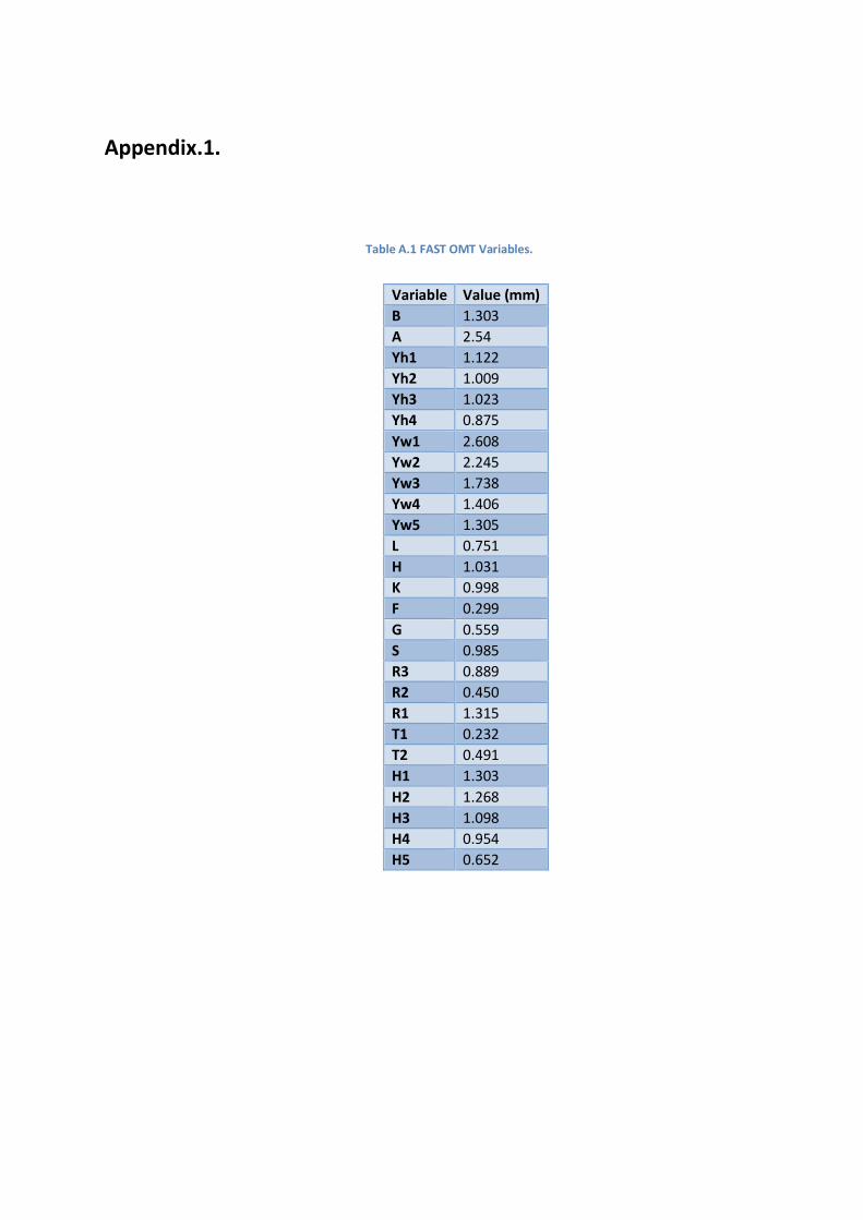
Appendix.1.
Table A.1 FAST OMT Variables.
Variable Value (mm)
B 1.303
A 2.54
Yh1 1.122
Yh2 1.009
Yh3 1.023
Yh4 0.875
Yw1 2.608
Yw2 2.245
Yw3 1.738
Yw4 1.406
Yw5 1.305
L 0.751
H 1.031
K 0.998
F 0.299
G 0.559
S 0.985
R3 0.889
R2 0.450
R1 1.315
T1 0.232
T2 0.491
H1 1.303
H2 1.268
H3 1.098
H4 0.954
H5 0.652