design and implementation of a dsp based controller for power
TRANSCRIPT
Design and Implementation of a DSP
Based Controller for Power Electronic
Applications
By
GERHARD J VAN HEERDEN
Thesis presented in partial fulfilment of the requirements for the
degree of Master of Science (Engineering) at the University of
Stellenbosch
Supervisor: Prof H Du T Mouton
April 2003

i
Declaration
I, the undersigned, hereby declare that the work contained in this thesis is my own original
work, unless otherwise stated, and has not previously, in its entirety or in part, been admitted at
any university for a degree.
...................................
Gerhard J van Heerden
1 December 2002

ii
Summary
In the field of power electronic engineering, there is a need for a reconfigurable power elec-
tronic controller. Such a controller will enable engineers to stay focussed on their main field
of study, not being side-tracked by the process of designing a high-speed digital controller to
implement their ideas with. The design, construction and implementation of such a controller is
presented in this paper. The design process involved defining the specifications of the controller
and finding electronic components to satisfy them. After suitable components had been iden-
tified, a schematic design of the system was done. The netlist of the schematic was exported
to a printed circuit board (PCB) design program, where the final layout was done and the con-
nections between the devices routed. Before the PCB was manufactured, the firmware for the
programmable logic devices (PLDs) was written to ensure that it fits in the selected PLDs of
the system. After the PCB was manufactured and all its components fitted, it was tested and
eventually used to implement the control of a shunt active power filter.

iii
Opsomming
Wanneer navorsing gedoen word in die drywings-elektronika gebied, word ’n behoefte vir ’n
heropstelbare drywings-elektroniese beheerder ondervind. So ’n beheerder sal ingenieurs in
staat stel om gefokus te bly op hulle hoof studieveld, sonder dat hulle aandag hoef te skenk
daaraan om ’n hoe spoed digitale beheerder te ontwerp om hulle idees mee te implementeer.
Die ontwerp, konstruksie en implementering van so ’n beheerder word in hierdie tesis voorgele.
Die ontwerp behels die bepaling van die spesifikasies van die beheerder en die opsporing van
elektroniese komponente wat hierdie spesifikasies sal bevredig. Nadat geskikte komponente
gevind is, is ’n skematiese ontwerp van die hele beheerder gedoen. Die lys van die verbindings
tussen die komponente (Eng. netlist) is na die stroombaanbord ontwerp program gestuur, waar
die finale uitleg van die bord gedoen is. Voordat die bord gemaak kon word, is die program-
matuur vir die programmeerbare logikatoestelle geskryf om te verseker dat dit in die toestelle
wat in die sisteem gebruik word, sal pas. Nadat die stroombaanborde vervaardig is en al die
komponente daarop gemonteer is, is die bord getoets en uiteindelik gebruik om die beheer van
’n aktiewe drywingsfilter te implementeer.

iv
Acknowledgements
I would like to thank the following people:
Mrs Stark, my high school mathematics teacher, for her support and all the effort she put into
teaching me and all of her students.
Prof Mouton for his guidance, assistance and the great opportunity that he gave me with this
project.
My family and friends for their support. I would especially like to thank Sone Kruger for her
loyal support even during difficult times.
The workshop staff who were always ready to help and offer advice.
The members of the Power Electronics Group of the University of Stellenbosch for their tech-
nical advice and support.
v
GlossaryAbbreviations
ADC Analog-to-digital converter
ASCII American standard code for information interchange
CLK Clock
COFF Common object file format
CPU Central processing unit
DAC Digital-to-analog converter
DSP Digital signal processor
EEPROM Electrically erasable programmable read-only memory
EPLD Erasable programmable logic device
FPGA Field-programmable gate array
FRAM Flash random-access memory
HIGH Logical ’1’
I/O Input or output
JTAG Joint test action group
LCD Liquid crystal display
LOW Logical ’0’
MFLOPS Million floating-point operations per second
MIPS Million instructions per second
MSPS Million samples per second
PCB Printed circuit board
PLD Programmable logic device
PWM Pulse-width modulation
RnW Read not write
ROM Read-only memory
RTC Real-time clock
SPI Serial peripheral interface
SQNR Signal-to-quantization noise error
SRAM Static random-access memory
SVPWM Space vector pulse-width modulation
USB Universal serial bus

vi
Symbols
C Capacitance
e�(n) Quantization error
f frequency
F� Sampling frequency
I� Phase A of the current supplied to the rectifier
I� Alpha component of the current supplied to the load
I� Phase B of the current supplied to the rectifier
I� Beta component of the current supplied to the load
I� Phase C of the current supplied to the rectifier
Iconv� Phase A of the current injected into the system by the filter
Iconv� Alpha component of the current injected into the system by the filter
Iconv� Phase B of the current injected into the system by the filter
Iconv� Beta component of the current injected into the system by the filter
Iconv� Phase C of the current injected into the system by the filter
L Inductance
p Instantaneous real power
p DC component of the instantaneous real power
p AC component of the instantaneous real power
p� Instantaneous real power supplied by filter
p Instantaneous real power supplied to load
P� Average power of a discrete-time signal
p� Instantaneous real power supplied by source
P Average power of a continuous-time signal
q Instantaneous imaginary power
q� Instantaneous imaginary power supplied by filter
q Instantaneous imaginary power supplied to load
q� Instantaneous imaginary power supplied by source
R Resistance
V� Phase A of the AC supply voltage
V� Alpha component of the AC supply voltage
V� Phase B of the AC supply voltage
V� Beta component of the AC supply voltage
V� Phase C of the AC supply voltage
x(n) Discrete-time signal
x�(t) Continuous-time signal

Contents
1 Introduction 1
1.1 A Comparison of Different Power Electronic Controller Systems . . . . . . . . 1
1.2 Thesis Outline . . . . . . . . . . . . . . . . . . . . . . . . . . . . . . . . . . . 2
2 Digital Control Systems 5
2.1 General Architecture . . . . . . . . . . . . . . . . . . . . . . . . . . . . . . . 5
2.2 Specifications of a Digital Controller . . . . . . . . . . . . . . . . . . . . . . . 6
2.2.1 The Analog-to-Digital Converter . . . . . . . . . . . . . . . . . . . . . 6
2.2.2 The Digital Signal Processor . . . . . . . . . . . . . . . . . . . . . . . 9
2.2.3 The Digital-to-Analog Converter . . . . . . . . . . . . . . . . . . . . . 9
2.3 Advantages and Disadvantages of Digital Control Systems . . . . . . . . . . . 9
3 Design of the Controller Hardware 11
3.1 Specifications of the System . . . . . . . . . . . . . . . . . . . . . . . . . . . 11
3.2 Overview of System Operation . . . . . . . . . . . . . . . . . . . . . . . . . . 12
3.3 Key Components of the System . . . . . . . . . . . . . . . . . . . . . . . . . . 14
3.3.1 The Digital Signal Processor . . . . . . . . . . . . . . . . . . . . . . . 14
3.3.2 The Programmable Logic Devices . . . . . . . . . . . . . . . . . . . . 19
3.3.3 The Analog-to-Digital Converters . . . . . . . . . . . . . . . . . . . . 25
3.3.4 The Digital-to-Analog Converters . . . . . . . . . . . . . . . . . . . . 27
3.3.5 The System Memory . . . . . . . . . . . . . . . . . . . . . . . . . . . 28
3.3.6 The Real-Time Clock . . . . . . . . . . . . . . . . . . . . . . . . . . . 29
3.3.7 The Universal Serial Bus Interface Device . . . . . . . . . . . . . . . . 29
3.4 Design of the Power Supply and Reset Circuitry . . . . . . . . . . . . . . . . . 31
3.4.1 The Power Supply Circuitry . . . . . . . . . . . . . . . . . . . . . . . 31
3.4.2 The Reset Circuitry . . . . . . . . . . . . . . . . . . . . . . . . . . . . 31
3.5 Design of the Printed Circuit Board . . . . . . . . . . . . . . . . . . . . . . . 35
4 Firmware Design for the Programmable Logic Devices 37
4.1 Design of the Common Programmable Logic Modules . . . . . . . . . . . . . 37
4.1.1 The Control of the Data Flow Between a FPGA and the DSP . . . . . . 37
vii

CONTENTS viii
4.1.2 The Processing of Commands . . . . . . . . . . . . . . . . . . . . . . 42
4.2 Design of the Firmware for FPGA Main . . . . . . . . . . . . . . . . . . . . . 45
4.2.1 The Control of the Flash RAM . . . . . . . . . . . . . . . . . . . . . . 45
4.2.2 The Control of the Real-Time Clock . . . . . . . . . . . . . . . . . . . 46
4.2.3 The Control of the Serial Communications . . . . . . . . . . . . . . . 49
4.2.4 The DSP Boot Controller . . . . . . . . . . . . . . . . . . . . . . . . . 55
4.2.5 The Data Bus Access Controller . . . . . . . . . . . . . . . . . . . . . 56
4.2.6 The Clock Generator . . . . . . . . . . . . . . . . . . . . . . . . . . . 57
4.3 Design of the Firmware for FPGA Analog . . . . . . . . . . . . . . . . . . . . 58
4.3.1 The Processing of Interrupts . . . . . . . . . . . . . . . . . . . . . . . 58
4.3.2 The Control of the Analog-to-Digital Converters . . . . . . . . . . . . 59
4.3.3 The Control of the Digital-to-Analog Converters . . . . . . . . . . . . 64
4.3.4 The Pulse-Width Modulation Interface . . . . . . . . . . . . . . . . . . 66
4.3.5 The Liquid Crystal Display Controller . . . . . . . . . . . . . . . . . . 69
4.3.6 The Keypad Controller . . . . . . . . . . . . . . . . . . . . . . . . . . 72
4.4 Design of the Firmware for EPLD ExBus . . . . . . . . . . . . . . . . . . . . 77
4.4.1 The Complete Expansion Bus Module . . . . . . . . . . . . . . . . . 77
4.4.2 The Expansion Bus Control Module . . . . . . . . . . . . . . . . . . 78
5 Test Implementation: Control of an Active Power Filter 81
5.1 Overview of the System . . . . . . . . . . . . . . . . . . . . . . . . . . . . . . 81
5.2 Theory of the Compensation Scheme . . . . . . . . . . . . . . . . . . . . . . . 81
5.2.1 Overview of the Control Scheme . . . . . . . . . . . . . . . . . . . . . 83
5.2.2 Instantaneous Reactive Power Theory . . . . . . . . . . . . . . . . . . 86
5.2.3 Space Vector Pulse-Width Modulation Theory . . . . . . . . . . . . . 89
5.3 Simulation of the System Using Simplorer . . . . . . . . . . . . . . . . . . . . 93
5.3.1 The Simulation Model . . . . . . . . . . . . . . . . . . . . . . . . . . 95
5.3.2 Results of the Simulation . . . . . . . . . . . . . . . . . . . . . . . . . 97
5.4 Implementation of the System . . . . . . . . . . . . . . . . . . . . . . . . . . 101
5.4.1 The System Hardware . . . . . . . . . . . . . . . . . . . . . . . . . . 101
5.4.2 Implementation of the Control Algorithm in the DSP . . . . . . . . . . 104
5.4.3 Results of Implementation . . . . . . . . . . . . . . . . . . . . . . . . 108
6 Conclusions 116
6.1 Summary of the Project . . . . . . . . . . . . . . . . . . . . . . . . . . . . . . 116
6.2 Thesis Contribution . . . . . . . . . . . . . . . . . . . . . . . . . . . . . . . . 116
6.3 Future Work and Recommendations . . . . . . . . . . . . . . . . . . . . . . . 117
CONTENTS ix
A Schematics 120
A.1 Schematics of the PEC33 . . . . . . . . . . . . . . . . . . . . . . . . . . . . . 120
A.2 Schematics of the PEC33 Optical Fibre Expansion Board . . . . . . . . . . . . 129
A.3 Schematics of the Voltage and Current Probes . . . . . . . . . . . . . . . . . . 132
B Printed Circuit Board Layouts 135
B.1 Printed Circuit Board Layout of the PEC33 . . . . . . . . . . . . . . . . . . . 135
B.2 Printed Circuit Board Layout of the PEC33 Optical Fibre Expansion Board . . 141
B.3 Printed Circuit Board Layout of the Voltage and Current Probes . . . . . . . . 144
C DSP C Example Programs 148
C.1 The Header File Containing the Address Definitions, PEC33 Address.h . . . . 149
C.2 The DSP C Program to Copy Serial Input Data to FRAM 0, SERIAL2FRAM.c . 152
C.3 The DSP C Program to Test the Liquid Crystal Display, LCD Test1.c . . . . . . 157
C.4 The DSP C Program to Test the Real-Time Clock, RTC Test.c . . . . . . . . . 161
C.5 The DSP C Program Implementing the Active Power Filter’s Control Algorithm 166
D PLD Firmware 180
D.1 Firmware for FPGA Main . . . . . . . . . . . . . . . . . . . . . . . . . . . . 180
D.1.1 Graphical Design File for FPGA Main . . . . . . . . . . . . . . . . . . 181
D.1.2 VHDL Code for the Addr Dec Ctrl Module of FPGA Main . . . . . . 184
D.1.3 VHDL Code for the Addr Element Module of FPGA Main . . . . . . . 188
D.1.4 VHDL Code for the Command Ctrl Module of FPGA Main . . . . . . 189
D.1.5 VHDL Code for the Data Ctrl Module of FPGA Main . . . . . . . . . 192
D.1.6 VHDL Code for the MyBuf Module of FPGA Main . . . . . . . . . . 196
D.1.7 VHDL Code for the BiDir Module of FPGA Main . . . . . . . . . . . 197
D.1.8 VHDL Code for the FRAM Ctrl Module of FPGA Main . . . . . . . . 199
D.1.9 VHDL Code for the RTC Ctrl Module of FPGA Main . . . . . . . . . 203
D.1.10 Graphical Design File for the SP Ctrl Module of FPGA Main . . . . . 215
D.1.11 VHDL Code for the UART Ctrl Module of FPGA Main . . . . . . . . 216
D.1.12 VHDL Code for the DSP SP TX Ctrl Module of FPGA Main . . . . . 227
D.1.13 VHDL Code for the DSP SP RX Ctrl Module of FPGA Main . . . . . 231
D.1.14 VHDL Code for the Dev Sel Ctrl Module of FPGA Main . . . . . . . 237
D.1.15 VHDL Code for the DSP Boot Ctrl Module of FPGA Main . . . . . . 240
D.1.16 VHDL Code for the Clk Gen Ctrl Module of FPGA Main . . . . . . . 243
D.2 Firmware for FPGA Analog . . . . . . . . . . . . . . . . . . . . . . . . . . . 244
D.2.1 Graphical Design File for FPGA Analog . . . . . . . . . . . . . . . . . 245
D.2.2 VHDL Code for the Addr Dec Ctrl Module of FPGA Analog . . . . . 250
D.2.3 VHDL Code for the Addr Element Module of FPGA Analog . . . . . . 264

CONTENTS x
D.2.4 VHDL Code for the Command Ctrl Module of FPGA Analog . . . . . 265
D.2.5 VHDL Code for the Data Ctrl Module of FPGA Analog . . . . . . . . 269
D.2.6 VHDL Code for the MyBuf Module of FPGA Analog . . . . . . . . . 288
D.2.7 VHDL Code for the BiDir Module of FPGA Analog . . . . . . . . . . 289
D.2.8 VHDL Code for the Interrupt Ctrl Module of FPGA Analog . . . . . . 291
D.2.9 VHDL Code for the ADC Ctrl Module of FPGA Analog . . . . . . . . 299
D.2.10 VHDL Code for the ADC Chan Generator Module of FPGA Analog . 304
D.2.11 VHDL Code for the ADC Data Store Module of FPGA Analog . . . . 306
D.2.12 VHDL Code for the DAC Ctrl Module of FPGA Analog . . . . . . . . 307
D.2.13 VHDL Code for the PWM Ctrl Module of FPGA Analog . . . . . . . 312
D.2.14 VHDL Code for the LCD Ctrl Module of FPGA Analog . . . . . . . . 323
D.2.15 VHDL Code for the KP Ctrl Module of FPGA Analog . . . . . . . . . 333
D.3 Firmware for EPLD ExBus . . . . . . . . . . . . . . . . . . . . . . . . . . . . 336
D.3.1 VHDL Code for the ExBus Single Complete Module of EPLD ExBus . 337
D.3.2 VHDL Code for the ExBus Ctrl Module of EPLD ExBus . . . . . . . . 341
D.3.3 VHDL Code for the BiDir Module of EPLD ExBus . . . . . . . . . . . 348

List of Figures
2.1 General Architecture of a Digital Control System . . . . . . . . . . . . . . . . 5
2.2 General Architecture of a Digital Controller . . . . . . . . . . . . . . . . . . . 6
2.3 Parts of an Analog-to-Digital Converter . . . . . . . . . . . . . . . . . . . . . 7
2.4 The Quantization Error . . . . . . . . . . . . . . . . . . . . . . . . . . . . . . 8
3.1 Block Diagram of the PEC33 Controller . . . . . . . . . . . . . . . . . . . . . 13
3.2 DSP Serial Boot Flow Chart . . . . . . . . . . . . . . . . . . . . . . . . . . . 17
3.3 Graphical User Interface of the PEC33 Serial Data Interface Application . . . . 18
3.4 DSP FRAM Load and Boot Flow Chart . . . . . . . . . . . . . . . . . . . . . 20
3.5 DSP 14-Pin Header Signals and Dimensions (figure taken from [10]) . . . . . . 21
3.6 Connection of the DSP to the Emulator Header (figure taken from [10]) . . . . 22
3.7 Device Configuration with a Download Cable and a Configuration Device (fig-
ure taken from [14]) . . . . . . . . . . . . . . . . . . . . . . . . . . . . . . . . 24
3.8 JTAG-Chain Device Programming with a ByteBlaster Cable (figure taken from
[15]) . . . . . . . . . . . . . . . . . . . . . . . . . . . . . . . . . . . . . . . . 24
3.9 Block Diagram of the PEC33 Memory Organisation . . . . . . . . . . . . . . . 30
3.10 Block Diagram of the Current Requirements and Voltage Supply to the Key
Components of the System . . . . . . . . . . . . . . . . . . . . . . . . . . . . 33
3.11 Diagram Showing the Resistors Used to Set the Threshold Voltage of the TLC7701 34
3.12 Block Diagram of the Reset Circuitry of the System . . . . . . . . . . . . . . . 35
4.1 Diagram of the Data Ctrl Module . . . . . . . . . . . . . . . . . . . . . . . . 38
4.2 Detailed Diagram of the Data Flow Through the Data Ctrl Module . . . . . . . 39
4.3 Diagram of the Bidir Module . . . . . . . . . . . . . . . . . . . . . . . . . . . 39
4.4 Diagram of the MyBuf Module . . . . . . . . . . . . . . . . . . . . . . . . . . 40
4.5 Diagram of the Addr Dec Ctrl Module of FPGA Main . . . . . . . . . . . . . 41
4.6 Diagram of the Addr Dec Ctrl Module of FPGA Analog . . . . . . . . . . . . 41
4.7 Diagram of the Addr Element Module of FPGA Main . . . . . . . . . . . . . . 42
4.8 Diagram of the Addr Element Module of FPGA Analog . . . . . . . . . . . . . 42
4.9 Diagram of the Command Ctrl Module . . . . . . . . . . . . . . . . . . . . . 44
4.10 Diagram of the FRAM Ctrl Module . . . . . . . . . . . . . . . . . . . . . . . 45
xi

LIST OF FIGURES xii
4.11 State Flow Chart of the FRAM Ctrl Module . . . . . . . . . . . . . . . . . . . 46
4.12 Diagram of the RTC Ctrl Module . . . . . . . . . . . . . . . . . . . . . . . . 47
4.13 Mode Flow Chart of the RTC Ctrl Module . . . . . . . . . . . . . . . . . . . . 47
4.14 State Flow Chart of the RTC Ctrl Module . . . . . . . . . . . . . . . . . . . . 48
4.15 Diagram of the SP Ctrl Module . . . . . . . . . . . . . . . . . . . . . . . . . 49
4.16 Diagram of the Components of the SP Ctrl Module . . . . . . . . . . . . . . . 51
4.17 Reception State Flow Chart of the UART Ctrl Module . . . . . . . . . . . . . . 52
4.18 Transmission State Flow Chart of the UART Ctrl Module . . . . . . . . . . . . 53
4.19 Reception State Flow Chart of the DSP SP RX Ctrl Module . . . . . . . . . . 54
4.20 Transmission State Flow Chart of the DSP SP RX Ctrl Module . . . . . . . . . 54
4.21 State Flow Chart of the DSP SP TX Ctrl Module . . . . . . . . . . . . . . . . 55
4.22 Diagram of the DSP BOOT Ctrl Module . . . . . . . . . . . . . . . . . . . . . 56
4.23 Diagram of the DEV SEL Ctrl Module . . . . . . . . . . . . . . . . . . . . . . 56
4.24 Diagram of the CLK GEN Ctrl Module . . . . . . . . . . . . . . . . . . . . . 57
4.25 Diagram of the Interrupt Ctrl Module . . . . . . . . . . . . . . . . . . . . . . 59
4.26 Diagram of the ADC Ctrl Module . . . . . . . . . . . . . . . . . . . . . . . . 61
4.27 State Flow Chart of the ADC Ctrl Module . . . . . . . . . . . . . . . . . . . . 62
4.28 Diagram of the ADC Chan Generator Module . . . . . . . . . . . . . . . . . 63
4.29 Diagram of the ADC Data Store Module . . . . . . . . . . . . . . . . . . . . 64
4.30 Diagram of the DAC Ctrl Module . . . . . . . . . . . . . . . . . . . . . . . . 65
4.31 State Flow Chart of the DAC Ctrl Module . . . . . . . . . . . . . . . . . . . . 67
4.32 Diagram of the PWM Ctrl Module . . . . . . . . . . . . . . . . . . . . . . . . 69
4.33 State Flow Chart of the PWM Ctrl Module . . . . . . . . . . . . . . . . . . . . 70
4.34 Diagram of the LCD Ctrl Module . . . . . . . . . . . . . . . . . . . . . . . . 71
4.35 LCD State Flow Chart of the LCD Ctrl Module . . . . . . . . . . . . . . . . . 72
4.36 Data State Flow Chart of the LCD Ctrl Module . . . . . . . . . . . . . . . . . 73
4.37 Read State Flow Chart of the LCD Ctrl Module . . . . . . . . . . . . . . . . . 74
4.38 Write State Flow Chart of the LCD Ctrl Module . . . . . . . . . . . . . . . . . 74
4.39 Diagram of the KEYPAD Ctrl Module . . . . . . . . . . . . . . . . . . . . . . 75
4.40 Diagram of the Switch Configuration of the Keypad . . . . . . . . . . . . . . . 76
4.41 Diagram of the ExBus Single Complete Module . . . . . . . . . . . . . . . . . 77
4.42 Diagram of the Components of the ExBus Single Complete Module . . . . . . 78
4.43 State Flow Chart of the ExBus Ctrl Module . . . . . . . . . . . . . . . . . . . 79
5.1 Block Diagram of the System and the Shunt Active Power Filter . . . . . . . . 82
5.2 Block Diagram of the Power Flows in the System . . . . . . . . . . . . . . . . 82
5.3 Graph and Schematic of Filter Inductor Currents and Voltages . . . . . . . . . 84
5.4 Flow Chart of the Control Algorithm . . . . . . . . . . . . . . . . . . . . . . . 85
5.5 Block Diagram of the Calculation of the PWM Reference Values . . . . . . . . 85
LIST OF FIGURES xiii
5.6 Graph of the Timing of the PWM Reference Signals . . . . . . . . . . . . . . . 86
5.7 Graph of the abc and �-� Coordinate Systems . . . . . . . . . . . . . . . . . . 87
5.8 Graph of the Instantaneous Space Vectors . . . . . . . . . . . . . . . . . . . . 88
5.9 Graph of the Space Vector PWM Sectors . . . . . . . . . . . . . . . . . . . . . 90
5.10 Graph of the Voltage Reference in Sector 1 . . . . . . . . . . . . . . . . . . . 90
5.11 Flow Chart of Algorithm to Calculate the Sector . . . . . . . . . . . . . . . . . 91
5.12 Graph of SVPWM References and Corresponding Switch Signals . . . . . . . 92
5.13 Simulation Schematic of the System . . . . . . . . . . . . . . . . . . . . . . . 95
5.14 Schematic of the Control State Machine . . . . . . . . . . . . . . . . . . . . . 96
5.15 Schematic of the PWM State Machine . . . . . . . . . . . . . . . . . . . . . . 97
5.16 Instantaneous Real and Imaginary Power Delivered by Source . . . . . . . . . 98
5.17 Three-phase Source Currents . . . . . . . . . . . . . . . . . . . . . . . . . . . 98
5.18 Three-phase Currents Supplied to the Three-phase Rectifier . . . . . . . . . . . 98
5.19 The Voltage Across the Load . . . . . . . . . . . . . . . . . . . . . . . . . . . 99
5.20 The Current Supplied to the Load . . . . . . . . . . . . . . . . . . . . . . . . 99
5.21 Three-phase Currents Injected by the Filter and their References . . . . . . . . 100
5.22 � and � Components of the Supply Voltage and the Reference Voltages of the
Converter . . . . . . . . . . . . . . . . . . . . . . . . . . . . . . . . . . . . . 100
5.23 Schematic of the System . . . . . . . . . . . . . . . . . . . . . . . . . . . . . 101
5.24 Schematic of the Voltage Divider . . . . . . . . . . . . . . . . . . . . . . . . . 102
5.25 Power Supply Configuration of the System . . . . . . . . . . . . . . . . . . . . 104
5.26 Diagram of the Signal Conversions Involved in Measuring the Supply Voltage . 107
5.27 Diagram of the Signal Conversions Involved in Measuring the Current Supplied
to the Load . . . . . . . . . . . . . . . . . . . . . . . . . . . . . . . . . . . . 107
5.28 Diagram of the Signal Conversions Involved in Measuring the Current Injected
into the System by the Inverter . . . . . . . . . . . . . . . . . . . . . . . . . . 107
5.29 Graph of the Unfiltered Source and Load Currents . . . . . . . . . . . . . . . . 109
5.30 Graph of the AC Component of the Instantaneous Real Power and Instantaneous
Imaginary Power with the Filter Disabled . . . . . . . . . . . . . . . . . . . . 110
5.31 Graph of the � and � Components of the Reference for the Converter Currents
with the Filter Disabled . . . . . . . . . . . . . . . . . . . . . . . . . . . . . . 110
5.32 Graph of the Alpha Component of the Supply Voltage and its Reference with
the Filter Disabled . . . . . . . . . . . . . . . . . . . . . . . . . . . . . . . . . 111
5.33 Graph of the Supply Current, Load Current and the Current Injected by the
Filter in Phase A of the System . . . . . . . . . . . . . . . . . . . . . . . . . . 112
5.34 Graph of the AC Component of the Instantaneous Real Power and Instantaneous
Imaginary Power Delivered to the Rectifier with the Filter Enabled . . . . . . . 112

LIST OF FIGURES xiv
5.35 Graph of the Alpha Component of the Current Injected by the Filter and its
Reference . . . . . . . . . . . . . . . . . . . . . . . . . . . . . . . . . . . . . 113
5.36 Graph of the Alpha Component of the Supply Voltage and its Reference with
the Filter Enabled . . . . . . . . . . . . . . . . . . . . . . . . . . . . . . . . . 113
5.37 Graph of the FFT of the Supply, the Load and the Converter Currents with the
Filter Enabled . . . . . . . . . . . . . . . . . . . . . . . . . . . . . . . . . . . 114
5.38 Graph of the FFT of the Supply Current with the Filter Enabled and Disabled . 115
A.1 Schematic of the DSP and Flash RAM of the PEC33 Controller . . . . . . . . . 121
A.2 Schematic of FPGA Main of the PEC33 Controller . . . . . . . . . . . . . . . 122
A.3 Schematic of FPGA Analog of the PEC33 Controller . . . . . . . . . . . . . . 123
A.4 Schematic of the Ports and Drivers of the PEC33 Controller . . . . . . . . . . . 124
A.5 Schematic of the Analog-to-Digital Converters of the PEC33 Controller . . . . 125
A.6 Schematic of the Digital-to-Analog Converters of the PEC33 Controller . . . . 126
A.7 Schematic of EPLD ExBus and the Expansion ports of the PEC33 Controller . 127
A.8 Schematic of the Power Supply and Reset Circuitry of the PEC33 Controller . . 128
A.9 Schematic of the Optical Fibre Transmitters of the PEC33 Expansion Board . . 130
A.10 Schematic of the Optical Fibre Receivers of the PEC33 Expansion Board . . . 131
A.11 Schematic of the Voltage Probes . . . . . . . . . . . . . . . . . . . . . . . . . 133
A.12 Schematic of the Current Probes . . . . . . . . . . . . . . . . . . . . . . . . . 134
B.1 Printed Circuit Board Layout of the PEC33 TOP and BOTTOM Silk Layers . . 136
B.2 Printed Circuit Board Layout of the PEC33 TOP Layer . . . . . . . . . . . . . 137
B.3 Printed Circuit Board Layout of the PEC33 BOTTOM Layer . . . . . . . . . . 138
B.4 Printed Circuit Board Layout of the PEC33 POWER Layer . . . . . . . . . . . 139
B.5 Printed Circuit Board Layout of the PEC33 Ground Layer . . . . . . . . . . . 140
B.6 Printed Circuit Board Layout of the Expansion Board TOP Layer . . . . . . . . 142
B.7 Printed Circuit Board Layout of the Expansion Board BOT Layer . . . . . . . 143
B.8 Printed Circuit Board Layout of the Current and Voltage Probes TOP and BOT-
TOM Silk Layers . . . . . . . . . . . . . . . . . . . . . . . . . . . . . . . . . 145
B.9 Printed Circuit Board Layout of the Current and Voltage Probes TOP Layers . . 146
B.10 Printed Circuit Board Layout of the Current and Voltage Probes BOTTOM Layers147
D.1 Graphical Design File of FPGA Main (Part 1 of 3) . . . . . . . . . . . . . . . . 181
D.2 Graphical Design File of FPGA Main (Part 2 of 3) . . . . . . . . . . . . . . . . 182
D.3 Graphical Design File of FPGA Main (Part 3 of 3) . . . . . . . . . . . . . . . . 183
D.4 Graphical Design File of the SP Ctrl Symbol . . . . . . . . . . . . . . . . . . 215
D.5 Graphical Design File of FPGA Analog (Part 1 of 5) . . . . . . . . . . . . . . 245
D.6 Graphical Design File of FPGA Analog (Part 2 of 5) . . . . . . . . . . . . . . 246
D.7 Graphical Design File of FPGA Analog (Part 3 of 5) . . . . . . . . . . . . . . 247

LIST OF FIGURES xv
D.8 Graphical Design File of FPGA Analog (Part 4 of 5) . . . . . . . . . . . . . . 248
D.9 Graphical Design File of FPGA Analog (Part 5 of 5) . . . . . . . . . . . . . . 249

List of Tables
1.1 Comparison of Available Power Electronic Controller Boards . . . . . . . . . . 3
3.1 DSP Header Signal Descriptions . . . . . . . . . . . . . . . . . . . . . . . . . 21
3.2 The Configuration Bits of the Analog-to-Digital Converters . . . . . . . . . . . 26
3.3 The Configuration Bits of the Digital-to-Analog Converters . . . . . . . . . . . 28
3.4 The Address Map of the Real-Time Clock . . . . . . . . . . . . . . . . . . . . 31
3.5 Current Requirements of Devices in mA . . . . . . . . . . . . . . . . . . . . . 32
3.6 Voltage Regulators Used in the System . . . . . . . . . . . . . . . . . . . . . . 32
4.1 The Definition of Command Register 0 of FPGA Main . . . . . . . . . . . . . 43
4.2 The Definition of Command Register 1 of FPGA Main . . . . . . . . . . . . . 43
4.3 The Definition of Command Register 0 of FPGA Analog . . . . . . . . . . . . 43
4.4 The Definition of Command Register 1 of FPGA Analog . . . . . . . . . . . . 44
4.5 The Control Signals Generated During Each State by the FRAM Ctrl module . 46
4.6 The Definition of the Interrupt Enable Register . . . . . . . . . . . . . . . . . 58
4.7 The Definition of the Interrupt Register . . . . . . . . . . . . . . . . . . . . . 59
4.8 The Interface of the ADC Ctrl Module to an ADC . . . . . . . . . . . . . . . . 60
4.9 The Interface of the ADC Ctrl Module to the Rest of FPGA Analog . . . . . . 60
4.10 The Interface of the ADC Chan Generator Module . . . . . . . . . . . . . . . 62
4.11 The Interface of the ADC Data Store Module . . . . . . . . . . . . . . . . . . 63
4.12 The Interface of the DAC Ctrl Module to a DAC . . . . . . . . . . . . . . . . 64
4.13 The Interface of the DAC Ctrl Module to the Rest of FPGA Analog . . . . . . 65
4.14 The Duration of each wr state and rd state State-Machine State . . . . . . . . . 73
4.15 The Encoding of the Keypad . . . . . . . . . . . . . . . . . . . . . . . . . . . 75
5.1 Coefficients for Calculating Voltage Space Vector Duty Cycles for Each Sector 93
5.2 PWM Switching Sequences and References for Each Sector . . . . . . . . . . 94
xvi
Chapter 1
Introduction
The focus of this thesis is the development of a general purpose power electronic controller,
which is flexible in its applications, and easy to set up and use. The controller had to be able
to take voltage measurements, do complex calculations with these measurements as inputs, and
be able to generate and transmit pulse-width modulated or analog control signals. The need
for such a controller arose because power electronic engineers do not always have the time or
technical expertise to design complex high-speed digital controllers to handle the control of the
power electronic system that they are researching. Having a reconfigurable power electronic
controller which is ready to be used, will save power electronic engineers a great deal of time
and will ensure that they can stay focused on the main area of their research.
1.1 A Comparison of Different Power Electronic Controller
Systems
As mentioned above, the controller consists of three main sections, which is determined by the
functions to be performed. The first section is responsible for the sampling of the measurements,
the second for processing of the samples and the calculation of the control signals, and the third
for supplying the control signals to the system to be controlled. One method is to implement
these sections on separate printed circuit boards which can be connected either by some type of
cable or by inserting the one board directly into a socket provided on the other. This modular
approach has the advantage that sections not needed does not have to be included in the system.
A disadvantage of having separate boards is that by severing the direct connection between
two devices, noise is introduced onto their interface. The other method is to combine all three
sections into one printed circuit board. This approach has the advantages that it minimizes the
distance between devices and that solid ground and power planes can be used which reduce
the noise in the system. Table 1.1 is a comparison of three power electronic controller systems
with the PEC33 controller. The PEC33 controller was designed to replace the PEC31 controller.
The most important enhancement that was made when designing the PEC33, was the use of the
1

CHAPTER 1 — INTRODUCTION 2
improved C3x DSP, the TMS320VC33. This DSP executes instructions faster, and it has more
internal SRAM, which makes external SRAM unnecessary. Another improvement was made
by using the TLV1570 analog-to-digital converters instead of the AD7891 converters that was
used on the PEC31 controller. The new ADCs sample and deliver the data almost twice as fast
as the ADCs used on the PEC31 controller.
The next controller in the table is the EP31-CPU from Interface Concepts. A modular approach
was used in designing this controller. It consists of a main board, the EP31-CPU, which contains
the DSP, PLDs, memory and communications ports, and one or two of the EP30-EXT1-x plug-
in boards. The plug-in boards contain the analog input and PWM output ports. The values
provided in the table for this controller, are for the combination of the main module, the EP31-
CPU and two of the EP30-EXT1-x extension modules. The control module contains the same
DSP as the PEC33 controller, but almost four times more non-volatile memory. The most
important difference between the extension boards and the PEC33 is the total conversion time
of the ADCs. The conversion times of the ADCs used in the PEC33 controller is almost three
times faster than the conversion time of the ADCs used in the EP30-EXT1-x extension modules.
Another difference is that the PEC33 has 32 analog input channels, while two of the extension
boards only has 16 in total.
The MU-DSP240-LPI, which was developed by the Power Electronics Group of Monash Uni-
versity in Australia, is another example of a nonmodular design. It was developed specifically
to control three-phase inverters. At its core it has the TMS320F240 DSP which is optimized for
digital motor control applications. Two of the advanced peripherals that this DSP contains to
enable it to be used in these applications are 12 PWM outputs and 16 ADC input channels.
The major advantages of the PEC33 controller are therefore the amount of analog input channels
(32) and the high analog to digital conversion speeds that it provides to the user. Controlling
the system with the TMS320VC33-150 floating-point controller and providing outputs for two
complete PWM blocks, makes the PEC33 controller an extremely versatile and useful tool for
the power electronic engineer.
1.2 Thesis Outline
To introduce some of the concepts that influence the design of a digital controller, chapter 2
discusses digital control systems briefly. The discussion starts with a section on the general
architecture of a digital control system and continues with a more detailed examination of the
specifications influencing the operation of each part of the control system. The chapter con-
cludes with some advantages and disadvantages of using a digital control system.
Chapter 3 discusses the design of the hardware of the PEC33 controller. The first sections
provide the system requirements and a brief explanation on how the system operates. The third
section discusses the hardware design principles and decisions made with respect to some of

CHAPTER 1 — INTRODUCTION 3
Name PEC33 PEC31 EP31-CPU MU-DSP240-LPI
+ 2 � FP30-EXT1-x
Manufacturer Power Electronics Group, Power Electronics Group, Interface Concepts Power Electronics Group,
University of Stellenbosch University of Stellenbosch Monash University
DSP TMS320VC33-150 TMS320C31-33 TMS320VC33-150 TMS320F240
Fixed/Floating Floating Floating Floating Fixed
Point Arithmatic
MFLOPS 150 33.3 150 NA
MIPS 75 16.7 75 20
Data Bus Width 32-Bit 32-Bit 32-Bit 16-Bit
Address Space 16M (24-Bit) 16M (24-Bit) 16M (24-Bit) 224k
Serial Ports 1 1 1 2
ADC Channels None None None 16 (10-Bit)
PWM Channels None None None 12
PLDs
FPGAs 2 x EP1K50 1 x EPM81500 1 x EP1K30, 1 x EP1K50 Unknown
EPLDs 2 x EPM7256B 1 x EPF7128S None Unknown
Memory
(DSP) Internal
SRAM 34k (32-Bit) 2k (32-Bit) 34k (32-Bit) 544 (16-Bit)
FRAM/EPROM None None None 16k (16-Bit)
(DSP) External
SRAM None 32k (32-Bit) 128k (32-Bit) 128k (16-Bit)
FRAM/EPROM 512k (8-Bit) 512k (32-Bit) 2M (8-Bit) 64k (16-Bit)
Communication
Ports
RS-232 Yes No Yes Yes
DSP Emulator JTAG Parallel C31 JTAG JTAG
DSK Interface
Other USB ISA Bus CAN Bus SPI
Analog Inputs 32 (10-Bit) 32 (12-Bit) 16 (11-Bit) 10 (10-Bit)
Analog Outputs 8 (12-Bit) 4 (12-Bit) None Unknown
PWM Outputs 2 � 2 � 4 + 2 2 � 2 � 4 + 2 2 � 2 � 4 2 � 4
Power Supply 5V, 2A (Max) 5V, 2A (Min) 5V, 2A; �12V, 440mA Unknown
Table 1.1: Comparison of Available Power Electronic Controller Boards

CHAPTER 1 — INTRODUCTION 4
the main devices of the system. Section four discusses the design of the power supply and reset
circuitry of the system. The final section provides some of the principles employed in making
the layout of the printed circuit board.
Chapter 4 discusses the design and operation of the firmware for the programmable logic de-
vices. The first two sections focuses on firmware modules implemented in both FPGA Main
and FPGA Analog. In the subsequent sections, the firmware designed exclusively for FPGA
Main, FPGA Analog and EPLD Exbus is examined.
Chapter 5 discusses the implementation of a shunt active power filter utilizing the PEC33 con-
troller to implement the compensation scheme. The chapter consists of sections discussing the
theory of the compensation scheme, the simulation model and results, the practical implemen-
tation of the system and the results obtained.
Chapter 2
Digital Control Systems
This chapter discusses the general architecture of the control system, some of the specifications
of digital controllers that have to be examined before deciding on a controller, and the advan-
tages and disadvantages of using digital control systems. In the next chapter the design of the
controller hardware will be discussed.
2.1 General Architecture
This section gives a short description of the general architecture of the digital control system
and digital controller. The next section will examine some of the main specifications of the
digital controller which determines its usefulness in a specific control system.
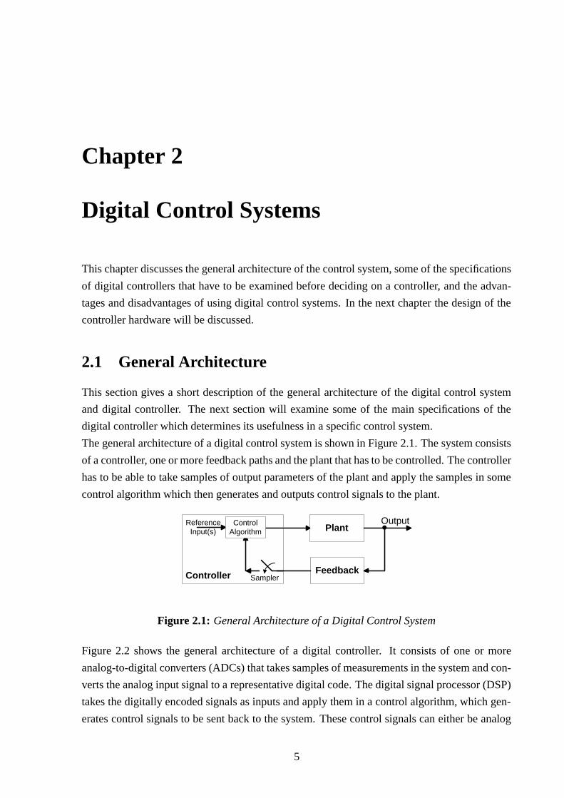
The general architecture of a digital control system is shown in Figure 2.1. The system consists
of a controller, one or more feedback paths and the plant that has to be controlled. The controller
has to be able to take samples of output parameters of the plant and apply the samples in some
control algorithm which then generates and outputs control signals to the plant.
Plant
Feedback
ReferenceInput(s)
Output
SamplerController
ControlAlgorithm
Figure 2.1: General Architecture of a Digital Control System
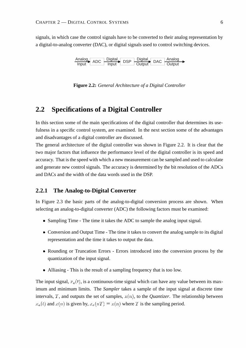
Figure 2.2 shows the general architecture of a digital controller. It consists of one or more
analog-to-digital converters (ADCs) that takes samples of measurements in the system and con-
verts the analog input signal to a representative digital code. The digital signal processor (DSP)
takes the digitally encoded signals as inputs and apply them in a control algorithm, which gen-
erates control signals to be sent back to the system. These control signals can either be analog
5
CHAPTER 2 — DIGITAL CONTROL SYSTEMS 6
signals, in which case the control signals have to be converted to their analog representation by
a digital-to-analog converter (DAC), or digital signals used to control switching devices.
ADC DSP DACAnalogInput
DigitalInput
DigitalOutput
AnalogOutput
Figure 2.2: General Architecture of a Digital Controller
2.2 Specifications of a Digital Controller
In this section some of the main specifications of the digital controller that determines its use-
fulness in a specific control system, are examined. In the next section some of the advantages
and disadvantages of a digital controller are discussed.
The general architecture of the digital controller was shown in Figure 2.2. It is clear that the
two major factors that influence the performance level of the digital controller is its speed and
accuracy. That is the speed with which a new measurement can be sampled and used to calculate
and generate new control signals. The accuracy is determined by the bit resolution of the ADCs
and DACs and the width of the data words used in the DSP.
2.2.1 The Analog-to-Digital Converter
In Figure 2.3 the basic parts of the analog-to-digital conversion process are shown. When
selecting an analog-to-digital converter (ADC) the following factors must be examined:
� Sampling Time - The time it takes the ADC to sample the analog input signal.
� Conversion and Output Time - The time it takes to convert the analog sample to its digital
representation and the time it takes to output the data.
� Rounding or Truncation Errors - Errors introduced into the conversion process by the
quantization of the input signal.
� Alliasing - This is the result of a sampling frequency that is too low.
The input signal, �����, is a continuous-time signal which can have any value between its max-
imum and minimum limits. The Sampler takes a sample of the input signal at discrete time
intervals, � , and outputs the set of samples, ����, to the Quantizer. The relationship between
����� and ���� is given by, ����� � � ���� where � is the sampling period.

CHAPTER 2 — DIGITAL CONTROL SYSTEMS 7
Sampler Quantizer Coderxa(t) x(n) xq(n) 01001...
AnalogSignal
Discrete-TimeSignal
QuantizedSignal
DigitalSignal
Figure 2.3: Parts of an Analog-to-Digital Converter
If we take a closer look at discrete-time sinusoids, it can be shown that they have a limited range
of possible frequencies:
��
�� � � �
��� �
�
where � is the frequency in cycles per sample,
is the frequency of the analog input signal in Hertz, and
� is the sampling frequency in Hertz.When the frequency of the discrete-time sinusoid falls outside this region, that is when � �� , the discrete time sinusoid is indistinguishable from a signal with a frequency inside the
region and it is impossible to recover the original signal from the discrete-time version. From
theory explained in [2], the frequencies � � � �, �� � � � ( is an integer) are
indistinguishable from the frequency � after sampling. This phenomenon is called alliasing.
Care must therefore be taken to ensure that the sampling frequency is more than twice the
highest frequency component of the signal to be sampled to prevent alliasing.
The Quantizer takes ���� as input and outputs the quantized signal, �����, which is a discrete-
time, discrete-valued signal. It can only obtain a value from a closed set of values. This implies
that the input to the Quantizer has to be either rounded or truncated to a value in the allowed
set of values. The error introduced in the system by this process is called the quantization error
and is simply the difference between ���� and �����. The size of the quantization error is a
value from the range,
��
�� ����� �
�
�(2.1)
where � is the quantization step.
The quantization step is the difference between two adjacent values in the set of allowed values
and is given by the following equation:
� ���� � ����
�� �(2.2)
where ��� is the maximum value of the signal
���� is the minimum value of the signal
� is the number of quantization levels.

CHAPTER 2 — DIGITAL CONTROL SYSTEMS 8
From eq. 2.1 and eq. 2.2 it is clear that the quantization error can be reduced by increasing the
number of quantization levels, �. Since the number of quantization levels is related to the bit
resolution of the ADC, the quantization step size can be redefined as:
� ��
��(2.3)
where � is the entire range of the ADC, and
� is the bit resolution of the ADC.From eq. 2.1 and eq. 2.3 it is clear that for every increase of one bit in the resolution of the
ADC, the quantization error is halved. The quality of the output of the ADC can be measured
with the signal-to-quantization noise ratio (SQNR) which is the ratio of the signal power to the
noise power,
SQNR ��
��
(2.4)
If we take sinusoidal signals as an example, we observe that between two quantization levels
the signal is almost linear. Figure 2.4 shows this linearization. The mean-square error power is
given by the following equation:
�� ��
��
� �
����������
��
�
� �
�
�������� (2.5)
where ����� � � �������� � � � � .
2
2
eq(t)
tττ
τ0τ t
Figure 2.4: The Quantization Error
If we substitute this equation for ����� into eq. 2.5 then,
�� ��
�
� �
�
��
��������
� ���
��� (2.6)
From eq. 2.6 it is clear that the mean-square error power is directly proportional to the square of
the quantization step size. The average power, �, of the sinusoidal signal, ����� � ������
is,
� ��
��
� ��
�
� ����������
� � �
�� (2.7)

CHAPTER 2 — DIGITAL CONTROL SYSTEMS 9
The SQNR for a sinusoidal signal is then by substituting eq.s 2.3, 2.6, 2.7 into the equation for
the SQNR, eq. 2.4:
SQNR ��
��
� ��
����� (2.8)
or
SQNR(dB) � ��log��SQNR
� �� � � ����� (2.9)
Eq. 2.9 implies that for every bit added the SQNR improves by 6 dB.
The Coder is the final stage in the analog-to-digital conversion process. It converts the quantized
samples to some digital format and outputs the digital signal.
2.2.2 The Digital Signal Processor
The digital signal processor can take many forms. The possibilities range from a powerful
personal computer to a small programmable microprocessor. The digital signal processor is
able to execute complex control algorithms and provides the capability to change the algorithms
through a change in the software of the processor.
The processor’s system clock initiates every action. Therefore, the system clock determines
the speed with which the processor can sample data, do calculations and generate outputs.
In selecting a processor, the width of its data words (measured in bits) have to be taken into
account, as this directly influences the accuracy of the calculations performed.
2.2.3 The Digital-to-Analog Converter
The digital-to-analog converter (DAC) converts a digital input signal to a representative analog
output signal. The DACs are simpler than the analog-to-digital converters (ADCs) since they
only have to decode the digital input signal and no other operation that may degrade the signal
accuracy, is performed. The DAC’s accuracy is determined by its bit resolution. If the width
of the processor’s data word is greater than that of the DAC, a type of quantization has to take
place inside the processor to convert the intended output data to the correct width. This process
will degrade the accuracy of the system.
2.3 Advantages and Disadvantages of Digital Control Sys-
tems
In this section some of the advantages and disadvantages of a digital control system are dis-
cussed.
CHAPTER 2 — DIGITAL CONTROL SYSTEMS 10
One of the greatest advantages of digital control systems is the reprogrammability of the control
algorithm and the flexibility it provides in controlling a system. This implies that by changing
the software of the digital controller, the control algorithm can be changed without the need to
change any of the hardware of the system. In addition, depending on the strength and flexibility
of the controller, the control algorithm can be very complicated. The fact that the data is in
digital format ensures that it can easily be stored, even for long periods. Control of the system
accuracy is easier, depending on the resolution of the ADCs and DACs. The implementation
of the system is sometimes cheaper, due to the smaller processor size and overall weight of
the system. A disadvantage of digital control systems is that the mathematical analysis and
design of the system is more complex than for a purely analog system. When a continuous-data
control system is converted to a sampled data system without changing the system parameters,
the stability of the system is decreased. The sampling of the input signal implies that there is a
loss of signal information that could degrade system performance.
Chapter 3
Design of the Controller Hardware
In this chapter the design of the PEC33 controller’s hardware is discussed. It starts with a section
on the specifications of the new controller and continues with sections on the components used
in the system and the printed circuit board design principles applied.
3.1 Specifications of the System
This section presents the specifications of the PEC33 power electronic controller. In the next
section the selection of the most important components is discussed.
The goals in designing the power electronic controller were to make it as flexible and easy to
use as possible. To accomplish this the following specifications were defined:
� Programmable floating-point processor in which to implement the control algorithm
� Programmable logic devices to generate control signals for devices on the controller
� 32 x Analog-to-digital conversion input channels
� 8 x Digital-to-analog conversion output channels
� Non-volatile storage medium for processor software and data
� 2 sets of 4 pairs of pulse-width modulation outputs
� Liquid crystal display and keypad to interface directly with user
� A real-time clock to accurately keep time and date information
The following ports for interfacing were also defined:
� Pulse-width modulation ports:
– 1 x Port providing 18 output channels
11

CHAPTER 3 — DESIGN OF THE CONTROLLER HARDWARE 12
– 1 x Port providing 18 error input channels
� Analog input and output ports:
– 4 x Analog-to-digital ports each providing 8 input channels
– 1 x Digital-to-analog port providing 8 output channels
� Data communication ports:
– 1 x RS-232 communications port
– 1 x Universal serial bus port
– 2 x Optical fiber transmitters
– 2 x Optical fiber receivers
– 2 x Reconfigurable expansion ports
� 1 x DSP emulator port
� User interfaces:
– 1 x Liquid crystal display port
– 1 x Keypad port
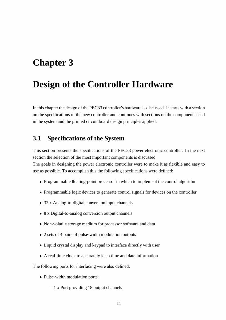
Figure 3.1 is a block diagram of the PEC33 Controller. It shows the key components of the
system and the connections between them.
3.2 Overview of System Operation
This section provides a brief description of how the system operates and how each component
fits into the overall system. In the next section the most important devices used in the system
are examined.
The most important devices used in the control of the system are the digital signal processor
(DSP) and the programmable logic devices (PLDs). The DSP executes a software program that
implements the control algorithm. The program decides which action needs to be taken and
when. To control an external device like an analog-to-digital converter (ADC), the DSP writes
to a specific register in the appropriate PLD. The PLD uses the data in its registers to send
control signals to the devices connected to it.
CHAPTER 3 — DESIGN OF THE CONTROLLER HARDWARE 13
Plug-in board
LC
D32
PDIUSBD12
ST3232CRS232 PORT
Cellular Phone PORT
USB PORT
ElectricalPWM
signalsOptical18
18
PWM Errorsignals
18
18
AM29LV200
HFBR1521
PeripheralDrivers
Analog-to-digital converters
Digital-to-analog converters
DSPTMS320VC33-150
Flash RAM
FPGA MainEP1K50QC208
DS1307
KE
YP
AD
FPGA AnalogEP1K50QC208
Real-Time Clock
Co
mm
un
icat
ion
Po
rts
[0..9]
[0..23]
[0..15]
[0..15]
Optical Fibre Ports
Co
ntr
ol s
ign
als
Inte
rru
pts
Inte
rru
pts
Ser
ial
Co
mm
un
icat
ion
[0..23]
[0..31]
AD5322BRMLPF83
3
3
3
3
3
3
3
TLV1570CDW 1
1
1
1
Electrical
Optical
AD5322BRM
AD5322BRM
AD5322BRM
LPF
LPF
LPF
TLV1570CDW
TLV1570CDW
TLV1570CDW
8
8
8
8
EPLDExBus0
EPM7256B
EPLDExBus1
EPM7256B
AM29LV200
ExB
us1
[0..15]
DA
TA
AD
DR
ES
S
[0..15]
ExB
us0
[0..15]
[0..15]
[0..7]
[0..7][0..17]
[0..17]
HFBR2521
HFBR1521
HFBR2521
HFBR1521
HFBR2521
Figure 3.1: Block Diagram of the PEC33 Controller

CHAPTER 3 — DESIGN OF THE CONTROLLER HARDWARE 14
3.3 Key Components of the System
In this section the most important devices used in the system are examined. Attention will be
given to what the advantages and disadvantages of the device are. The design of the power
supply and reset circuitry is discussed in section 3.4.
3.3.1 The Digital Signal Processor
A digital signal processor (DSP) has the advantages that it implements some instructions in
hardware and that it has on-chip memory. Both of these features enable the DSP to execute
instructions faster than other types of processors. When deciding on a DSP, the most important
choice is whether to use a fixed-point or floating-point processor. In fixed-point processors the
numbers are either fractions between -1.0 and +1.0 or integers. Fixed-point arithmetic is gen-
erally faster and less expensive than floating-point arithmetic. In floating-point arithmetic the
numbers are represented by a mantissa and an exponent. The value of the number is calculated
with the following expression:
value � mantissa� �exponent
This makes it possible to have a greater range of possible numbers.
The TMS320VC33-150 DSP from Texas Instruments was used in the PEC33 controller. Some
of its features are:
� High Performance Floating-Point Digital Signal Processor:
– 13 ns Instruction cycle
– 150 Million floating-point operations per second (MFLOPS)
– 75 Million instructions per second (MIPS)
� 34K � 32-Bit on-chip dual-access SRAM configured in 2 � 16K plus 2 � 1K Blocks
� �5 phase-locked loop clock generator
� 32-Bit high-performance CPU
� 16-/32-Bit integer and 32-/40-bit floating-point operations
� 32-Bit Instruction word, 24-bit address
� On-chip Memory-mapped peripherals:
– 1 � Serial port
– 2 � 32-Bit timers

CHAPTER 3 — DESIGN OF THE CONTROLLER HARDWARE 15
– DMA coprocessor for concurrent I/O and CPU operation
� Parallel ALU and multiplier execution in a single cycle
As previously mentioned, the internal memory of the DSP is volatile. This implies that every-
time the system is powered-up, the PEC33 system has to boot the DSP from some non-volatile
source. The system was designed to perform this task from three different sources. The first
two sources are either a personal computer indirectly connected to the DSP’s serial port, or
from FRAM. The third source which also makes debugging of the DSP program easier, is a
DSP emulation interface. This interface consists of a 14-pin port connected by an emultion pod
to a XDS510 board which is installed in a personal computer. With the Code Composer Studio
(version 4.10) software installed on the personal computer, the user can load the DSP programs
and debug it.
Booting the DSP through its Serial Port
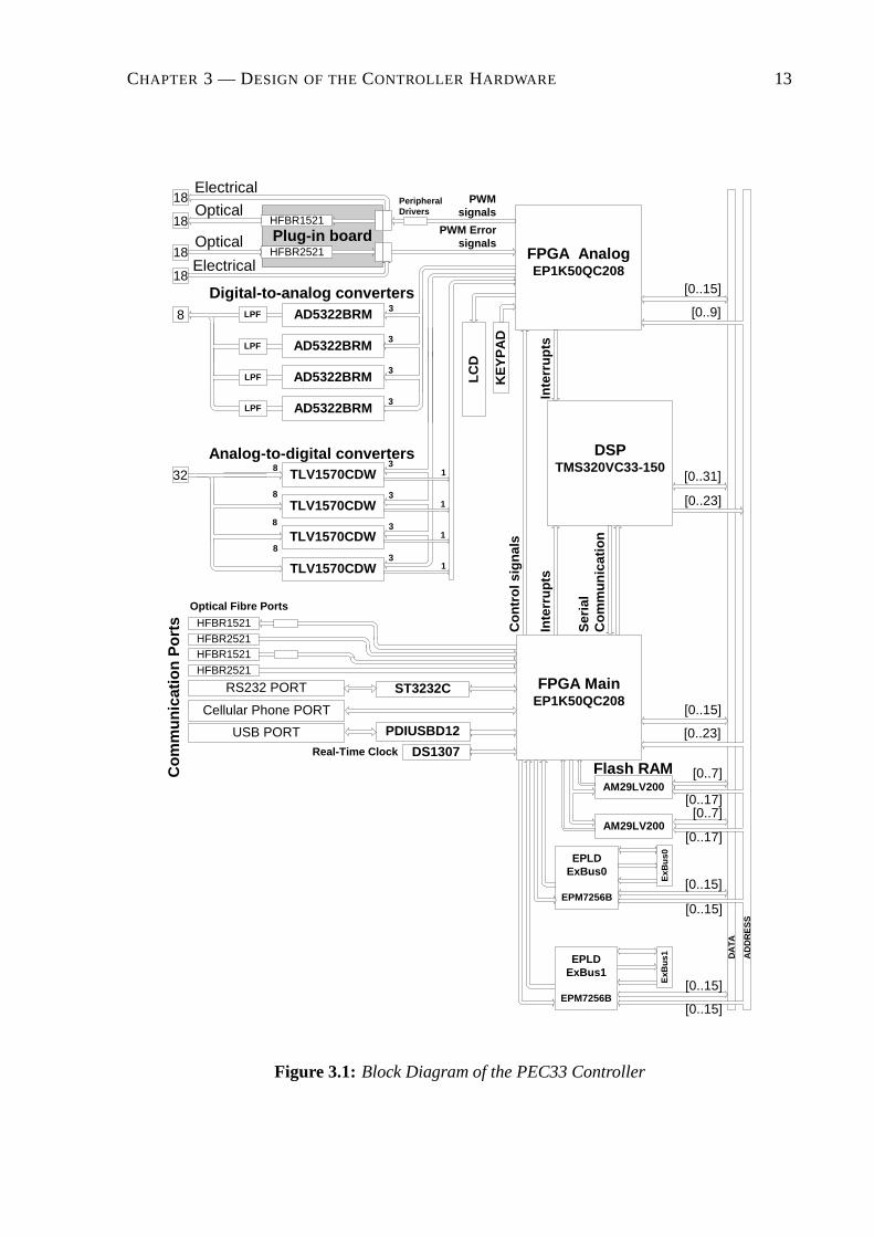
The serial boot process which is summarized in Figure 3.2, has three stages. The first stage
involves generating the binary common object file format (COFF) executable object. This is
accomplished by building (compiling, assembling and linking) the source program in the Code
Composer environment creating two output files, the COFF file, file.out and the map file. The
map file is an output file, created by the linker, that shows the memory configuration, section
composition, and section allocation, as well as symbols and the addresses at which they were
defined. The second stage involves the conversion of the COFF output file to a standard ASCII
format. This is done with the Hex30.exe program. The program is invoked with the following
command-line parameters:
file.out:
This parameter identifies the COFF file to be converted.
-a:
This specifies that the format of the output file should be the ASCII-Hex object format.
-romwidth 32:
This parameter specifies how the hexadecimal conversion utility partitions the data into output
files. The number of files is equal to the memory width divided by the ROM width. For a serial
load the memory width is 32. This implies that in order to get a single 32-bit output file, the
ROM width has to be 32.
-boot:
This parameter converts all sections into bootable form.
-bootorg SERIAL:
This parameter specifies that the DSP is to be booted from its serial port.
-o file.hex:
This parameter identifies the output file.

CHAPTER 3 — DESIGN OF THE CONTROLLER HARDWARE 16
A detailled explanation of all these parameters can be found in chapter 10, ”Hex Conversion
Utility Description”, of [9].
The last stage involves transfering the program to the DSP. This task is accomplished by the
PEC33SerialDataInterface.exe application. Figure 3.3 presents the graphical user interface of
this application. By clicking on the Select File button the user can browse for the ASCII-Hex
file that is to be transferred to the DSP. Before the actual program data can be transferred to
the DSP, a dummy data block is sent to the DSP. This data block has a size of 0x1, an address
equal to the code entry point of the program and one data element of value 0x0. It is necessary
to send this data block first since the DSP automatically starts executing the program loaded
in its memory at the address given in the first block of data it receives. The transmitting of
this dummy block with the address of the entry point, ensures therefore that the program starts
executing at the correct address. The default entry point assigned by the C compiler, c int00, is
obtained from the map file created when the project was linked. The entry point must be entered
into the Program Starting Address textbox. To prepare the system for the serial boot procedure,
dip switch 0 should be switched to the ON position which is the setting for a serial boot of
the system. The system must then be reset either by power cycling or by pressing the reset
pushbutton. After all the preparations are completed, the serial boot process can be initiated
by clicking on the Send Serial Boot Program button. The serial data transfer application sends
the dummy block first and then the data contained in the ASCII-Hex file. Each block of data
transferred to the system is described by a two element header transferred prior to the data. The
first element in the header is the size or number of 32-bit words in the data block. The second
element is the destination address of the data. After the system received a data block, it waits
for the next one. Only when a block size of zero is received, will the DSP stop waiting for more
data, reset itself, and start executing its program at the entry point address.
Booting the DSP from the Flash RAM
Booting of the DSP from the flash RAM is an automatic process once the program data has
been stored in the correct format and with the correct headers on the flash RAM. The tasks
to be performed in order to get the data onto the flash RAM are summarized in Figure 3.4.
The transfer of the program to the flash RAM has three stages. The first and second stages
are completed with the PEC33SerialDataInterface.exe application. In the first stage the DSP
is booted serially with a program that will receive and store data received by its serial port and
then re-transmit it to the flash RAM. The ASCII-Hex file of this program is shown in the DSP
Copy Program textbox and its code entry point in the DSP Copy Program Address textbox. In
the second stage the program data and headers are copied to the DSP. The programming file is
prepared in precisely the same way as described for the serial boot process. The first header
copied to the DSP defines parameters used to setup the DSP when the program is loaded from
the flash RAM during the flash RAM boot process. The first element is the width (in bits) of
CHAPTER 3 — DESIGN OF THE CONTROLLER HARDWARE 17
BuildProject
MapFile
file.out
Size of block 1
DSP
Data of block 1
Destination of block 1
Size of block 2
Data of block 2
Destination of block 2
file.hexSize = 0x00000001
Data = 0x00000000
Code entry point address
Size of last block
Data of last block
Destination of last block
Size of block 3
0x00000000
Dummyblock
Figure 3.2: DSP Serial Boot Flow Chart

CHAPTER 3 — DESIGN OF THE CONTROLLER HARDWARE 18
Figure 3.3: Graphical User Interface of the PEC33 Serial Data Interface Application

CHAPTER 3 — DESIGN OF THE CONTROLLER HARDWARE 19
the flash RAM (8 in this case) and the second is the value of the data bus strobe control register
during the transfer process. The value of the strobe control register is entered in the Primary
Bus Control Register textbox. The second header is the same dummy block as defined for
booting the DSP serially which defines the code entry point. The entry point is again entered
into the Program Starting Address textbox. The last word transferred is a zero word. The first
two stages are completed by switching dip switch 0 to the ON position which is the setting for
the a serial boot of the system and then clicking on the Send FRAM Boot Program button. The
third stage involves copying the data received by the DSP to the flash RAM. When this had been
done, the DSP can boot from the flash RAM. To boot the DSP from the flash RAM, dip switch
0 should be switched to the OFF position which is the setting for the flash RAM boot of the
system. When the system is reset, the data is read from the flash RAM. The first element read is
the memory width parameter, and the second the value of the primary bus control register. This
is followed by the elements of the dummy block and eventually the program data. The end of
program data transfer is signalled by the transfer of the zero word to the DSP. The DSP then
resets itself and starts executing from the code entry address.
The Emulation of the DSP
Emulation of the DSP is performed using the Code Composer environment. Emulation of the
DSP enables the user to have almost total control over the actions of the DSP. The personal
computer is connected to the DSP using a XDS510 emulator board inserted in a 16-bit ISA slot
of the computer and a JTAG cable. The installation of the XDS510 emulator is discussed in
more detail in the document XDS51x Emulator Installation Guide[11]. The header of the JTAG
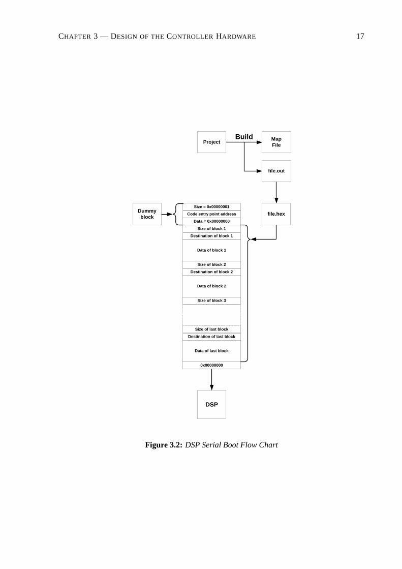
cable is shown in Figure 3.5. Table 3.1 provides a brief description of the functions of each pin.
Figure 3.6 illustrates how the DSP should be connected to the emulator header. Since the
distance between the DSP and the header was less than six inches, no buffering of any of the
signals was necessary. For more detailed information on the design requirements of the XDS510
emulator refer to the document JTAG/MPSD Emulation Technical Reference[10].
3.3.2 The Programmable Logic Devices
The programmable logic devices (PLDs) were added to the system to make the digital logic
design re-configurable. The task of the PLDs is to generate and send control signals to and
receive and decode signals received from the other devices in the controller system.
The Field-Programmable Gate Arrays
Two of the EP1K50QC208 ACEX series field-programmable gate arrays (FPGAs) from Altera
were used in the system. They are cheaper and faster than the older FLEX series devices.

CHAPTER 3 — DESIGN OF THE CONTROLLER HARDWARE 20
Serial2FRAM.hex
BuildProject
MapFile
file.out
Size of block 1
DSP
Data of block 1
Destination of block 1
Size of block 2
Data of block 2
Destination of block 2
file.hexSize: 0x00000001
Data = 0x00000000
Code entry point address
Size of last block
Data of last block
Destination of last block
Size of block 3
0x00000000
Dummyblock
Memory width: 0x00000001
Strobe control reg. value
FRAM 0
DSP
FRAM 0
Size of block 1
DSP
Data of block 1
Destination of block 1
Size of block 2
Data of block 2
Destination of block 2
Size = 0x00000001
Data = 0x00000000
0x00809994
Size of last block
Data of last block
Destination of last block
Size of block 3
0x00000000
Figure 3.4: DSP FRAM Load and Boot Flow Chart
CHAPTER 3 — DESIGN OF THE CONTROLLER HARDWARE 21
Figure 3.5: DSP 14-Pin Header Signals and Dimensions (figure taken from [10])
Signal Description Emulator Target
State State
TMS Test mode select Output Input
TDI Test data input Output Input
TDO Test data output Input Output
TCK Test clock of 10.368MHz Output Input
TRST Test reset Output Input
EMU0 Emulation pin 0 Input Input/
Output
EMU1 Emulation pin 1 Input Input/
Output
PD(Vcc) Presence detect Input Output
TCK RET Test clock return is the test clock input to the emulator. Input Output
GND Ground
Table 3.1: DSP Header Signal Descriptions

CHAPTER 3 — DESIGN OF THE CONTROLLER HARDWARE 22
Figure 3.6: Connection of the DSP to the Emulator Header (figure taken from [10])
These devices also have the lower input/output supply voltage of +3.3V which reduces power
consumption. The reason why two devices were included in the system is that one device does
not have enough input/output pins available. The logic functions were divided between the two
FPGAs as follows:
FPGA Main
� Controls external communication channels
� Controls access to the system data bus
� Controls access to the FRAM
� Controls the real-time clock
FPGA Analog
� Sends control signals to the ADCs and processes the received data
� Sends control and data signals to the DACs
� Generates and outputs the PWM signals
� Receives and processes PWM error input signals
� Controls a standard 2-line LCD
� Processes user input from a 4�3 keypad

CHAPTER 3 — DESIGN OF THE CONTROLLER HARDWARE 23
FPGAs have volatile internal memory which implies that like the DSP, the FPGAs must have a
non-volatile source for its programs. One EPC2LC20 configuration device from Altera is used
for this task. When the system is powered up, the EEPROM copies its data serially to the two
FPGAs. Figure 3.7 illustrates how multiple FPGAs can be programmed from one configuration
device with the same configuration data. The configuration setup used to program the FPGAs in
the PEC33 system is based on this topology. The only difference is that the two FPGAs should
not receive the same configuration data. To accomplish this, the FPGAs are connected in a data
chain by connecting the nCEO output of FPGA Main to the nCE input of FPGA Analog. The
first configuration file copied to the FPGAs will then configure FPGA Main. When FPGA Main
is configured, it drives its nCEO output LOW, enabling FPGA Analog to be configured by the
next configuration file received. The configuration device is configured using its JTAG ports
with a ByteBlaster cable connected to a personal computer. A single programming file (.pof)
is created and transfered to the configuration device. This file is the combination of the SRAM
object files (.sof) of the projects for the two FPGAs. To create the programming file, the Con-
vert SRAM Object Files option in the file menu of the MAX+Plus II program is used. When the
first prototype for the PEC33 controller was constructed, the configuration of the configuration
device worked without any problems. The only problem was the configuration device did not
automatically configure the FPGAs when the system was powered up. An error was discov-
ered in the datasheets describing the EPC2 configuration device. According to the datasheet,
the device has user-configurable 1k� internal pull-up resistors connected to its OE, nCS and
nINIT CONF pins. The idea is that the system can either be setup to use these internal resistors,
or external resistors can be used as illustrated in Figure 3.7. In the prototype of the PEC33
system, the external resistors (of 1k�) was connected, and the internal ones disabled with soft-
ware. The documentation error was that the internal pull-up resistor on the nINIT CONF
pin is always enabled and is NOT user-configurable. This meant that the effective pull-up
resistance connected to the pin was 500�. It was therefore unable to drive the pin LOW to
signal the start of the configuration of the FPGAs. Subsequently the resistor was removed, and
the FPGAs configured automatically without any difficulties.
The Erasable Programmable Logic Devices
One erasable programmable logic device (EPLD) for each of the two expansion busses of the
system are also included. The operation of the expansion busses is discussed in section 4.4.
The EPLDs used are the EPM7256B-100 in the MAX7000B series from Altera. Figure 3.8
illustrates how multiple devices (like the EPLDs) can be configured in a JTAG-chain. This is
the topology used to configure the EPLDs.

CHAPTER 3 — DESIGN OF THE CONTROLLER HARDWARE 24
Figure 3.7: Device Configuration with a Download Cable and a Configuration Device (figure
taken from [14])
Figure 3.8: JTAG-Chain Device Programming with a ByteBlaster Cable (figure taken from
[15])

CHAPTER 3 — DESIGN OF THE CONTROLLER HARDWARE 25
3.3.3 The Analog-to-Digital Converters
The analog-to-digital converters (ADCs) are used to convert analog input signals to a represen-
tative digital number. When selecting an ADC, the factors that influence its performance given
in section 2.2.1, have to be examined. The most important factors are the sampling rate, the
bit resolution and the number of input channels of the ADC. The number of input channels is
important, since a total of 32 input channels are needed in the system. The more input channels
per device, the less devices (and smaller board space) are required.
The ADC selected for the PEC33 controller is the TLV1570 from Texas Instruments. Some of
the features of these devices include:
� 10-Bit Resolution
� 1.25 MSPS sampling rate
� 8 Analog input channels
� Serial interface
The analog input range for this device is between 0V and a reference voltage supplied to one of
its pins. An external reference voltage of +4.096V was selected. This implies that the quantiza-
tion step size as defined in eq. 2.3 is:
� ��
���
�����V���
� �mV
The ADCs have the option to operate either from the external or two internal voltage references.
The system has therefore three voltage reference options configured by setting bits 5 and 6 of
the configuration word. The voltage reference possibilities are the abovementioned external
4.096V reference or either the 2.3V or 3.8V internal reference. To make the system even more
flexible, the DIP package of the component used to provide the external voltage reference, the
REF198 from Analog Devices, has been used. It is installed in a DIP socket making it possible
to exchange it for one of the other devices in the REF19x series.
In order to calculate the maximum sampling frequency of the ADCs, the specifications pro-
vided in their datasheet[16] is examined. The ADC takes 16 clock cycles to do a conversion
and the maximum clock input frequency is 20MHz, which gives the maximum sampling fre-
quency stated in its specifications ( �������
� ��������). The clock signal supplied to the
ADCs is 15MHz which gives a maximum sampling frequency of 937.5kSPS. This sampling
rate is further divided by the number of channels used. This implies that a maximum sampling
frequency of 117.1875kSPS is possible when sampling all 8 channels. A similar ADC with a
parallel interface is also available. The serial interface version was selected, because all four de-
vices can be controlled simultaneously with approximately the same amount of data and control
lines that one parallel interface device needs.

CHAPTER 3 — DESIGN OF THE CONTROLLER HARDWARE 26
Bit Number Description
Software power down:
15 0: Normal
1: Power down enabled
14 1: Reads out values of internal register
Self-test voltage to be applied during next clock cycle selection:
00: Analog input comes in normally
13..12 01: Analog ground is applied to analog input
10: Half the voltage reference is applied to the analog input
11: N/A
Operation speed selection:
11 0: High speed ( higher power consumption)
1: Low speed (lower power consumption)
10 Enabling of auto-scan function
9..7 Analog input channel selection
External or internal reference voltage selection
6 0: External
1: Internal
Internal reference voltage to be applied during the next clock cycle:
5 0: 2.3V (for 3V voltage supply)
1: 3.8V (for 5V voltage supply)
4 Enabling of autopower-down function
Performance optimizer
3 0: AV�� � 5.5V to 3.6V
1: AV�� � 3.5V to 2.7V
2..0 000 (Reserved bits)
Table 3.2: The Configuration Bits of the Analog-to-Digital Converters

CHAPTER 3 — DESIGN OF THE CONTROLLER HARDWARE 27
The ADCs have two interfacing modes. The first is a 5-wire serial interface and is called the
DSP mode. The other is a 4-wire serial interface and is called the Microcontroller mode. Since
the microcontroller mode requires one less interfacing pin per ADC, this mode was imple-
mented in the system. Each time a sample needs to be taken by one of these ADCs, a 16 bit
configuration word is sent to the ADC. Table 3.2 provides the definition of the control bits.
During the transfer of the last 10 configuration bits, the 10 bit data sample of the previous
conversion is sent back to the component controlling the ADC.
3.3.4 The Digital-to-Analog Converters
The digital-to-analog converters (DACs) are used to convert a digital number into a represen-
tative analog signal. Four of the AD5322 DACs from Analog Devices was used in the system.
Some of the features of the device are:
� 12-Bit
� 2-Channel
� 0.7 V/�s slew rate
� 8 �s output voltage settling time
From the device’s datasheet [17] the formula for calculating the output voltage is:
���� ����� ��
��(3.1)
where ���� is the reference voltage supplied to the DAC,
� is the decimal equivalent of the value loaded in the DAC’s register
� is the DAC’s resolution.The same 4.096V reference voltage source that was used for the ADCs, was also used to provide
the reference voltage to the DACs. When substituting the specific values for ���� and � into eq.
3.1, the following equation is obtained for the output voltage:
���� � ������� (3.2)
The difference between two voltage levels is then:
�����V���
� � mV
The fact that the reference voltage is provided by the same device that provides the reference
voltage to the ADCs implies that the same advantages apply. The only disadvantage is that
unlike the ADCs which have two different internal voltage references, the DACs can only use
this external source as a reference.
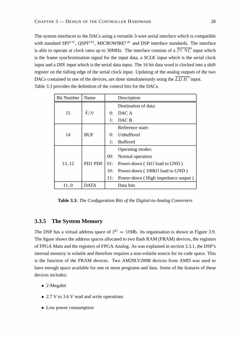
CHAPTER 3 — DESIGN OF THE CONTROLLER HARDWARE 28
The system interfaces to the DACs using a versatile 3-wire serial interface which is compatible
with standard SPI�� , QSPI�� , MICROWIRE�� and DSP interface standards. The interface
is able to operate at clock rates up to 30MHz. The interface consists of a �� �� input which
is the frame synchronization signal for the input data, a SCLK input which is the serial clock
input and a DIN input which is the serial data input. The 16 bit data word is clocked into a shift
register on the falling edge of the serial clock input. Updating of the analog outputs of the two
DACs contained in one of the devices, are done simultaneously using the �� � input.
Table 3.3 provides the definition of the control bits for the DACs.
Bit Number Name Description
Destination of data:
15 � �� 0: DAC A
1: DAC B
Reference state:
14 BUF 0: Unbuffered
1: Buffered
Operating modes:
00: Normal operation
13..12 PD1 PD0 01: Power-down ( 1k� load to GND )
10: Power-down ( 100k� load to GND )
11: Power-down ( High impedance output )
11..0 DATA Data bits
Table 3.3: The Configuration Bits of the Digital-to-Analog Converters
3.3.5 The System Memory
The DSP has a virtual address space of ��� � ��Mb. Its organisation is shown in Figure 3.9.
The figure shows the address spaces allocated to two flash RAM (FRAM) devices, the registers
of FPGA Main and the registers of FPGA Analog. As was explained in section 3.3.1, the DSP’s
internal memory is volatile and therefore requires a non-volatile source for its code space. This
is the function of the FRAM devices. Two AM29LV200B devices from AMD was used to
have enough space available for one or more programs and data. Some of the features of these
devices includes:
� 2-Megabit
� 2.7 V to 3.6 V read and write operations
� Low power consumption

CHAPTER 3 — DESIGN OF THE CONTROLLER HARDWARE 29
– 200 nA Standby mode current
– 7 mA Read current
– 15 mA Program/erase current
� Minimum of 1 000 000 write cycles guarantee per sector
3.3.6 The Real-Time Clock
The real-time clock (RTC) keeps the time and date information of the system up to date even
during power failures. This is important if data is to be automatically sampled and stored over
a certain period in the absence of an user. The DS1307 from Dallas Semiconductor was used.
Some of its features include:
� Counts seconds, minutes, hours, day of month, months and years with leap year compen-
sation
� Built-in power sense circuitry, which detects power failures and automatically switches
to battery supply
� 56 byte non-volatile RAM for data storage
� 2-wire serial interface
The system interfaces with the real-time clock using a 2-wire serial interface. The device is seen
as the slave and FPGA Main which controls it, is the master. The device has a 64 byte address
space which is shown in table 3.4. In the current configuration of the system the 56 bytes of
RAM is not utilized, but can be added if some need for it arises.
3.3.7 The Universal Serial Bus Interface Device
To allow for faster communications with the controller, a universal serial bus (USB) port was
implemented. To accomplish this, a USB interface device, the PDIUSBD12 from Philips Semi-
conductors, was added to the controller system. It has a high-speed parallel interface to the rest
of the system. Some of its features include:
� Complies with USB specification Rev. 1.1
� Contains internal FIFO memory
� High-speed 2Mbit/s parallel interface to any external microcontroller/processor
� Transfer rates:
– Bulk mode: 1MByte/s
– Isochronous mode: 1MBit/s

CHAPTER 3 — DESIGN OF THE CONTROLLER HARDWARE 30
Bootloader
DSP Boot Program+ Data
RAM Blocks 0-3+ Peripheral Bus
Registers
FP
GA
Mai
nF
lash
Ram
0F
PG
AA
nal
og
DS
PIn
tern
alM
emo
ryE
xBu
s 0
ExB
us
1F
lash
Ram
1Data
FFFh
100000h
200000h
300000h
400000h
500000h
600000h
700000h
800000h
900000h
A00000h
B00000h
C00000h
D00000h
E00000h
F00000h
60FFFFh
43FFFFh
C3FFFFh
A0FFFFh
B0FFFFh
Used
Unused
Figure 3.9: Block Diagram of the PEC33 Memory Organisation

CHAPTER 3 — DESIGN OF THE CONTROLLER HARDWARE 31
Address Function
00H Seconds
01H Minutes
02H Hours
03H Day
04H Date
05H Month
06H Year
07H Control
08H RAM... 56 � 8
3FH
Table 3.4: The Address Map of the Real-Time Clock
3.4 Design of the Power Supply and Reset Circuitry
This section discusses the design of the power supply and reset circuitry of the system. The
strategies used in designing the printed circuit board (PCB) are discussed in section 3.5.
3.4.1 The Power Supply Circuitry
The design process was complicated by the fact that four different voltage levels were needed
in the system. The four levels are +1.8V, +2.5V, +3.3V, +5V. Table 3.5 summarizes the current
requirements of the key components in the system.
The system has two +5V inputs to the controller. One supplies power to the peripheral drivers
driving the optical fiber transmitters, and one supplies the rest of the components on the board.
Figure 3.10 is a block diagram showing the current requirements and voltage supply topology
of the system. Table 3.6 is a summary of the voltage regulators used in the system showing their
output voltages and maximum output currents.
3.4.2 The Reset Circuitry
The reset circuitry of the system is shown in Figure 3.12. This configuration makes it possible
to monitor all the different voltage levels and reset the system when a dip occurs in any one of
the voltages. The LP2966IMM-1818 is a dual +1.8V voltage regulator with an open drain error
flag for each output. These error outputs are connected to the reset input pin of the adjustable
voltage supervisor, the TLC7701. The TLC7701 was setup to monitor the +2.5V supplied to

CHAPTER 3 — DESIGN OF THE CONTROLLER HARDWARE 32
Device +1.8V +2.5V +3.3V +5V
1 � DSP - Core 100
1 � DSP - I/O 150
2 � FPGA - Core 400
2 � FPGA - I/O 100
2 � EPLD - Core 400
2 � EPLD - I/O 100
2 � FRAM 60
4 � ADC 34
4 � DAC 1.8
1 � Configuration EEPROM 50
1 � LCD 2.5
1 � RS-232 Driver 2
1 � USB Interface 15
10� Peripheral Drivers 640
Table 3.5: Current Requirements of Devices in mA
Device Output Voltage Output Current
1 � LP2966IMM-1818 +1.8V 150mA
2 � LD1086DT25 +2.5V 1.5A
1 � LD1086DT33 +3.3V 1.5A
Table 3.6: Voltage Regulators Used in the System

CHAPTER 3 — DESIGN OF THE CONTROLLER HARDWARE 33
FPGAMain
FPGAAnalog
EPLDExBus0
EPLDExBus1
DSP
Other+5 V
Devices
1.8 V RegulatorLP2966IMM-1818
2.5 V RegulatorLD1086DT25
2.5 V RegulatorLD1086DT25
External+5V
Inputs
100 mA
200 mA
200 mA
200 mA
200 mA
50 mA
50 mA
50 mA
50 mA
150 mA
Other+3.3 V
Devices
127 mA
400 mA
400 mA
577 mA
9 x PeripheralDrivers
102.3 mA
576 mA1479.3 mA
3.3 V RegulatorLD1086DT33
100 mA
Figure 3.10: Block Diagram of the Current Requirements and Voltage Supply to the Key
Components of the System

CHAPTER 3 — DESIGN OF THE CONTROLLER HARDWARE 34
the FPGAs. The threshold voltage of the voltage supervisor is defined by two external resistors
connected to it. The connection of the resistors are shown in Figure 3.11. The equation for
calculating the threshold voltage is:
�� � ������� ���
��
(3.3)
The selected values of �� and �� was as close as possible to the values of the internal resistors of
the +2.5V voltage supervisor, the TLC7725 (the TLC7725 was unavailable when the controller
was designed, hence the use of an adjustable voltage supervisor). A value of 560k� was chosen
for both �� and �� giving (using eq. 3.4.2) a threshold voltage of +2.2V.
TLC7701
+2.5 V
SENSE
R1
R2
Figure 3.11: Diagram Showing the Resistors Used to Set the Threshold Voltage of the
TLC7701
The connection point of the +1.8V voltage regulator’s error flag pins and the TLC7701 voltage
supervisor’s reset input pin, is pulled high by a pull-up resistor during normal operation and
can be shorted to ground by pressing the connected pushbutton causing a reset event. The reset
output of the TLC7701 is connected to the reset input of the TLC7733 which is a voltage super-
visor monitoring the +3.3V voltage supply. The reset output of the TLC7733 is connected to the
reset input of FPGA Main. For both the TLC7701 and the TLC7733 there is a delay, ��, after
the reset input is deasserted or the sense voltage reaches the threshold voltage, during which
time the reset outputs are active (the system is in a reset state). This delay can be configured by
the value of the capacitor connected to the �� pin. From the datasheet of these devices [21] the
formula for calculating the capacitance is:
�� � ���� ��� � �� (3.4)
A delay of 10 ms was required. Selecting a value of 10 �F for �� provides a delay of 210 ms.
When the reset input to FPGA Main is driven low, the FPGA resets its internal logic circuits
and outputs reset signals to the DSP, FPGA Analog and the two EPLDs, EPLD ExBus0 and

CHAPTER 3 — DESIGN OF THE CONTROLLER HARDWARE 35
DSP
FPGAAnalog
EPLDExBus0
EPLDExBus1
+3.3 VVoltage
Supervisor
+2.5 VVoltage
Supervisor
+1.8 VVoltage
Regulator
ERROR1
ERROR2
PUSHBUTTON
+2.5 V +3.3 V
TLC7701 TLC7733
FPGAMain
RE
SIN
RE
SIN
RE
SE
T
RESET
RESET
RESET
RESET
LP2966IMM-1818
Figure 3.12: Block Diagram of the Reset Circuitry of the System
ExBus1. The fact that FPGA Main controls the reset signals to the DSP, FPGA Analog and
the EPLDs, makes it possible to disable the resetting of these components or to reset it in the
absense of any external fault condition.
3.5 Design of the Printed Circuit Board
In this, the last section of the chapter, the design of the printed circuit board is discussed.
Due to the complexity of the components used (large pin count, various supply voltage levels,
etc.) it was decided to use a four layer printed circuit board (PCB). Two layers, the TOP and
the BOTTOM layers, are signal layers and two layers, the POWER and GND layers, are plane
layers. All the connections, excluding the power and ground connections between the com-
ponents, are routed on the TOP and BOTTOM layers. The POWER layer consists of various
copper pours which supply the devices on the TOP and BOTTOM layers with the correct supply
voltages. It was necessary to have a separate layer for the power supplies to the devices, because
of the wide range of supply voltages needed by the devices and the overall complexity of the
PCB. The GND layer consists of one large copper pour which is the digital ground, and one
smaller copper pour which is the analog ground. The most important method of suppressing the
noise in the circuit is to separate the digital and analog grounds. These two planes should be
connected electrically by a single low impedance connection. The only exception is when work-
ing with analog-to-digital and digital-to-analog converters. For these devices both their analog
and digital ground pins should be connected by a low impedance path. Making this connection
inside these devices with an impedance that is low enough, is difficult due to the internal layout
of the devices. That is why the manufacturers rely on the user to supply the low impedance
path outside the device. Another advantage of using separate ground and power planes, is that
it provides better electromagnetic interference rejection. Low frequency signals follow the path

CHAPTER 3 — DESIGN OF THE CONTROLLER HARDWARE 36
of least resistance, but high frequency signals follow the path of least inductance [4]. For this
reason the returning currents flow directly under the the signal conductor minimizing the area
between them through which magnetic fields can pass and induce noise currents on the trans-
mission line. Because the two currents flow in opposite directions, it minimizes the effect of
radiated noise on the signal. This effect only works well when the plane is solid without gaps
and discontinuities which force the return currents to follow a path different from that of the
source signals. High frequency noise is also reduced by the distributed capacitance between the
ground and power plane. For a more detailed discussion on these concepts refer to chapter 17 of
”Op Amps for Everyone” [5] and the book entitled, High-Speed Digital Design - A Handbook
of Black Magic [4].
The layout of the devices and ports of the system can be seen in Figure B.1 which shows the
TOP and BOTTOM silk layers of the printed circuit board. As can be seen in the figure, all
the ports except the PWM ouput and error input ports are situated along the edge of the board
for easy access. The PWM ports were placed in the centre of the board making it possible
to connect the fiber optic expansion board without restricting access to the other ports of the
system. The devices processing analog signals (the ADCs and DACs) were placed together at
one end of the PCB. This made it easier to separate their ground planes. The expansion ports
were placed on the opposite edge of the PCB, one on the TOP and one on the BOTTOM layer
to make it possible to attach two piggy-back boards without them being in the way of the fiber
optic expansion board. To provide the main data and address busses to the two FPGAs, the DSP
was placed approximately in the centre of the PCB.

Chapter 4
Firmware Design for the Programmable
Logic Devices
In this chapter the design of the re-configurable hardware implemented with the programmable
logic devices is discussed. The PLDs enable the user to change the digital logic design of the
system providing a high level of flexibility in its applications. The system has the following
PLDs: two FPGAs, FPGA Main and FPGA Analog and two EPLDs, EPLD Exbus 0 and EPLD
Exbus 1. In the first section, the modules common to more than one PLD is discussed. In
subsequent chapters the modules implemented in specific PLDs are discussed.
4.1 Design of the Common Programmable Logic Modules
In this section the modules used to implement the same functions in different PLDs are dis-
cussed. In the next section the modules implemented exclusively in FPGA Main are discussed.
All the PLDs interface to the DSP via the data bus. Therefore, the first common task that has
to be performed in each of the PLDs, is to manage the flow of data between it and the DSP.
Section 4.1.1 will focus on how this is accomplished in FPGA Main and FPGA Analog. The
second common task that has to be performed, is to process commands sent to the PLDs by the
DSP. This will be discussed in section 4.1.2. The only function of the EPLDs is to interface the
DSP via its data bus to some external device connected to the expansion ports. In addition, the
interface between the DSP and the EPLDs differs from the DSP’s interface with the FPGAs.
Therefore, the transfer of data between the DSP and the EPLDs and their other functions is
discussed separately in section 4.4.
4.1.1 The Control of the Data Flow Between a FPGA and the DSP
The access to the data bus and the data flow is controlled by the DSP. It has absolute control over
the main address bus. The DSP is the master of the data bus and all the other devices accessing
it are slaves. In the FPGAs, the two main modules involved in the process of interfacing the
37
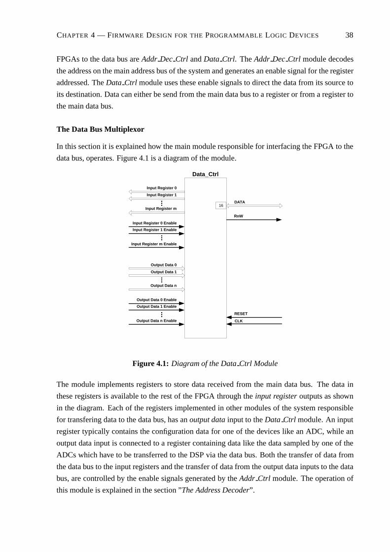
CHAPTER 4 — FIRMWARE DESIGN FOR THE PROGRAMMABLE LOGIC DEVICES 38
FPGAs to the data bus are Addr Dec Ctrl and Data Ctrl. The Addr Dec Ctrl module decodes
the address on the main address bus of the system and generates an enable signal for the register
addressed. The Data Ctrl module uses these enable signals to direct the data from its source to
its destination. Data can either be send from the main data bus to a register or from a register to
the main data bus.
The Data Bus Multiplexor
In this section it is explained how the main module responsible for interfacing the FPGA to the
data bus, operates. Figure 4.1 is a diagram of the module.
Input Register 0
CLK
RESET
Data_Ctrl
Input Register 1
Input Register m
Input Register 0 Enable
Input Register 1 Enable
Input Register m Enable
DATA16
RnW
Output Data 0
Output Data 1
Output Data n
Output Data 0 Enable
Output Data 1 Enable
Output Data n Enable
......
......
Figure 4.1: Diagram of the Data Ctrl Module
The module implements registers to store data received from the main data bus. The data in
these registers is available to the rest of the FPGA through the input register outputs as shown
in the diagram. Each of the registers implemented in other modules of the system responsible
for transfering data to the data bus, has an output data input to the Data Ctrl module. An input
register typically contains the configuration data for one of the devices like an ADC, while an
output data input is connected to a register containing data like the data sampled by one of the
ADCs which have to be transferred to the DSP via the data bus. Both the transfer of data from
the data bus to the input registers and the transfer of data from the output data inputs to the data
bus, are controlled by the enable signals generated by the Addr Ctrl module. The operation of
this module is explained in the section ”The Address Decoder”.

CHAPTER 4 — FIRMWARE DESIGN FOR THE PROGRAMMABLE LOGIC DEVICES 39
Figure 4.2 is a simplified diagram showing the interconnection of the modules used to imple-
ment the Data Ctrl module, emphasizing the data flow paths.
Input Register 0
CLK
RESET
Data_Ctrl
Input Register 1
Input Register m
Input Register 0 Enable
Input Register 1 Enable
Input Register m Enable
DATA
Output Data 0
Output Data 1
Output Data n
Output Data 0 Enable
Output Data 1 Enable
Output Data n Enable
......
OUT_DATABidir
BIDIR
IN_DATA
IN_DATA
SEL
MyBufOUT_DATA
IN_DATA
SEL
MyBufOUT_DATA
IN_DATA
SEL
MyBufOUT_DATA
......
CombinatorialMultiplexing Logic
Figure 4.2: Detailed Diagram of the Data Flow Through the Data Ctrl Module
To interface with the bi-directional data bus of the system, the Data Ctrl module contains a
Bidir module which is shown in Figure 4.3. Its BIDIR port is connected to the DATA port of
IN_DATA
RnW
CLK
Bidir
16BIDIR
16OUT_DATA
16
Figure 4.3: Diagram of the Bidir Module
Data Ctrl. When data is transferred from the data bus to the FPGA, the RnW input of the Bidir
module is driven HIGH, which causes the module to put its BIDIR ports in the high-Z state,
making it possible to read data placed on the data bus. The module outputs the data read on the
OUT DATA port. Another module was created to transfer the data from the OUT DATA output

CHAPTER 4 — FIRMWARE DESIGN FOR THE PROGRAMMABLE LOGIC DEVICES 40
to the correct destination module. The MyBuf module, shown in Figure 4.4 is a register. Its
operation is very simple. Whenever the SEL input is HIGH, the module’s data input (IN DATA)
is copied to its data output (OUT DATA) or else the data output stays the same. The SEL
inputs are provided by the enable signals originally created in the Addr Dec Ctrl module. The
IN DATA inputs of all the MyBuf registers were connected to the OUT DATA port of the Bidir
module. The OUT DATA outputs of the MyBuf module then provide the data to the rest of the
system. When data have to be transferred to the data bus, it is placed on the IN DATA input of
IN_DATA
SEL
RESET
MyBuf
nnOUT_DATA
Parameters: n: interger 0 to 15
Figure 4.4: Diagram of the MyBuf Module
the Bidir module. This proved to be a bit more complicated to implement, because the outputs
of more than one register have to be multiplexed to one data input. A modified MyBuf module
was created. Its output was like the previous version equal to its input when the SEL signal
was HIGH, but placed in the high-Z state when the SEL input is LOW. Although none of the
enables connected to the SEL inputs of the modified MyBuf modules (which is generated by
the Addr Dec Ctrl module) are ever active at the same time, the Max+Plus II compiler did not
allow this configuration stating that the IN DATA input has multiple sources. The problem was
solved by multiplexing each bit of the IN DATA input individually.
The Address Decoder
In this section the operation of the Addr Dec Ctrl module is discussed. This module is respon-
sible for the generation of the register enable signals that are sent to the Data Ctrl module.
Figure 4.5 and Figure 4.6 are diagrams showing the interfaces of Addr Dec Ctrl module for the
two FPGAs. The only difference is the inclusion of a strobe input, nSTRB, which is received
from the DSP in the Addr Dec Ctrl module implemented in FPGA Main. As can be seen in
the diagram, there are two types of enable signals, input register and output data enable signals
as explained in the previous section. The ADDR input is the 10 least significant bits of the
system’s main address bus. For FPGA Analog, the FPGA nCS input is received from FPGA
Main and is the combination of the active LOW chip select signal (��) for FPGA Analog and
the active LOW data bus strobe signal (����) generated by the DSP using a logical OR op-
eration. Therefore, only if both the chip select for FPGA Analog and the data bus strobe are
active (LOW), the chip select for the ADDR Dec Ctrl will be active. For FPGA Main the ��

CHAPTER 4 — FIRMWARE DESIGN FOR THE PROGRAMMABLE LOGIC DEVICES 41
and ���� input signals were kept seperate and only combined inside the module. The RESET
input is used to reset the module and the CLK input is the clock signal regulating the module.
CLK
RESET
Addr_Dec_Ctrl
Input Register 0 Enable
Input Register 1 Enable
Input Register m Enable
FPGA_nCS
Output Register 0 Enable
Output Register 1 Enable
Output Register n Enable...
...
ADDR10
nSTRB
Figure 4.5: Diagram of the Addr Dec Ctrl Module of FPGA Main
CLK
RESET
Addr_Dec_Ctrl
Input Register 0 Enable
Input Register 1 Enable
Input Register m Enable
FPGA_nCS
Output Register 0 Enable
Output Register 1 Enable
Output Register n Enable
......
ADDR10
Figure 4.6: Diagram of the Addr Dec Ctrl Module of FPGA Analog
The core of the Addr Dec Ctrl module is the Addr Element module. In actual fact the whole
Addr Dec Ctrl module is just a collection of these modules, one for each register which needs
an enable signal. Figure 4.7 and Figure 4.8 are the diagrams of this module for FPGA Main
and FPGA Analog respectively. Each of these modules has a unique address input constant
(INT ADDR) which corresponds to the address of the register represented by the particular
Addr Element module. This address is compared to the input address (ADDR) on every LOW to
HIGH transition of the input clock signal (CLK). For FPGA Main the enable output (EN) will be
activated only if the input address corresponds with the address constant and the logical OR of
the chip select signal (nCS), and the data strobe signal (nSTRB) is LOW. For FPGA Analog the
enable output will be activated only if the input address corresponds with the address constant
and the chip select signal (nCS) is LOW.

CHAPTER 4 — FIRMWARE DESIGN FOR THE PROGRAMMABLE LOGIC DEVICES 42
Parameters: INT_ADDR: interger 0 to 1023
CLK
RESET
Addr_Element
EN
nCS
ADDR10
nSTRB
Figure 4.7: Diagram of the Addr Element Module of FPGA Main
Parameters: INT_ADDR: interger 0 to 1023
CLK
RESET
Addr_Element
EN
nCS
ADDR10
Figure 4.8: Diagram of the Addr Element Module of FPGA Analog
4.1.2 The Processing of Commands
In this section the mechanism implemented for processing commands sent from the DSP to one
of the FPGAs is described. The module responsible for processing the commands is the Com-
mand Ctrl module. There are two types of commands implemented in the system. Commands
of type 0, trigger events like the loading of the DAC registers, while commands of type 1 enables
or disable modules. Figure 4.9 is a diagram of the interface of the module. CMD REG0 and
CMD REG1 are the outputs from the two command registers implemented in the DATA Ctrl
module. CMD REG0 is for commands of type 0 and COMMAND REG1 is for commands of
type 1. Each bit of these registers represents a different command. Table 4.1 and Table 4.2 are
the definitions of command registers 0 and 1 respectively for FPGA Main. The only command
implemented at present is the command to set the real-time clock. Table 4.3 and Table 4.4 are
the definitions of command registers 0 and 1 respectively for FPGA Analog.
Commands of type 0 are only executed when the CMD REG0 input changes to a value not equal
to ”00...0”. Therefore, to ensure that a command of type 0 is executed, it is advisable to reset
the command register by writing the zero word (”00...0”) to it. When commands of type 0 are
executed, the command outputs corresponding to bits set in the CMD REG0 input are pulsed
LOW for one clock cycle. The devices receiving these commands are all designed to react to
the LOW-to-HIGH transition of these signals.
The implementation of type 1 commands is much simpler since they only have to enable or

CHAPTER 4 — FIRMWARE DESIGN FOR THE PROGRAMMABLE LOGIC DEVICES 43
Bit Number Function
0 Real-time clock set
1 Reserved
2 Reserved
3 Reserved
4 Reserved
5 Reserved
6 Reserved
7 Reserved
Table 4.1: The Definition of Command Register 0 of FPGA Main
Bit Number Function
0 Reserved
1 Reserved
2 Reserved
3 Reserved
4 Reserved
5 Reserved
6 Reserved
7 Reserved
Table 4.2: The Definition of Command Register 1 of FPGA Main
Bit Number Function
0 Load DAC 0
1 Load DAC 1
2 Load DAC 2
3 Load DAC 3
4 Update LCD mode
5 Update LCD data
6 Reset LCD
Table 4.3: The Definition of Command Register 0 of FPGA Analog

CHAPTER 4 — FIRMWARE DESIGN FOR THE PROGRAMMABLE LOGIC DEVICES 44
Bit Number Function
0 Enable/disable ADC 0
1 Enable/disable ADC 1
2 Enable/disable ADC 2
3 Enable/disable ADC 3
4 Enable/disable PWM block 0
5 Enable/disable PWM block 1
Table 4.4: The Definition of Command Register 1 of FPGA Analog
disable modules. The command outputs receive the inverse of the CMD REG1 input on every
LOW-to-HIGH transition of the input clock signal, CLK.
CLK
RESET
Command_Ctrl
Commands of type 0 CMD_REG0n
Commands of type 1
CMD_REG1n
Figure 4.9: Diagram of the Command Ctrl Module
This section explained how the flow of data between the FPGAs and the DSP is controlled and
how commands are sent to the FPGAs and processed. In the next section the rest of the modules
implemented in FPGA Main is discussed.

CHAPTER 4 — FIRMWARE DESIGN FOR THE PROGRAMMABLE LOGIC DEVICES 45
4.2 Design of the Firmware for FPGA Main
In this section the firmware design for FPGA Main, is discussed. In the first section, the imple-
mentation of the flash RAM controllers is discussed. In subsequent sections the implementation
of the real-time clock and serial communications controllers, and the modules implemented to
generate the clock signals, the signals necessary to boot the DSP, and the chip select signals for
the devices accessing the main data bus, is discussed.
4.2.1 The Control of the Flash RAM
In this section the control of the flash RAM, the non-volatile storage medium of the system,
is discussed. The module responsible for controlling the flash RAM is the FRAM Ctrl module
which is shown in Figure 4.10. The system has two flash RAM devices, each controlled by
its own FRAM Ctrl module. The data and address ports of the devices are directly connected
to the system’s data and address busses respectively. The control signals are provided by the
FRAM Ctrl modules. Each device has its own chip enable input, but shares one output enable,
write enable and reset output from the FPGA. The sharing of these control inputs is possible,
because only when a device’s unique chip enable input is active, does the device react to these
control signals. The nEN input, which enables the module, is activated when the address on
the main address bus of the system is in the range assigned to the flash RAM device controlled
by the module. It then starts to generate the control signals to handle the current transaction
between the DSP and the flash RAM. The DSP nSTRB and DSP RnW inputs are the DSP’s
data bus strobe and read/write signals respectively. The FRAM Ctrl module has four states as
CLK
RESET
FRAM_Ctrl
FRAM_nCE
FRAM_nOE
FRAM_nWE
DSP_nSTRB
FRAM_nRST
DSP_RnW
nEN
Figure 4.10: Diagram of the FRAM Ctrl Module
shown in Figure 4.11. When it is not active, it is in the idle state state. The module becomes
active when both the nEN and DSP nSTRB signals are active (LOW). Depending on whether
it is a read or write transaction that is being performed, the state of the module will change to
either the rd state state for a read transaction or the wr state start state for a write transaction.
It will stay in the rd state state for seven clock cycles before returning to the idle state state.
It will stay in the wr state start state for four clock cycles before changing to the wr state end

CHAPTER 4 — FIRMWARE DESIGN FOR THE PROGRAMMABLE LOGIC DEVICES 46
state where it will stay for seven clock cycles before returning to the idle state state. Table 4.5
is a summary of the output levels of the control signals during each state.
State FRAM nCE FRAM nOE FRAM nWE FRAM nRST
idle state HIGH HIGH HIGH HIGH
rd state LOW LOW HIGH HIGH
wr state start LOW HIGH LOW HIGH
wr state end LOW HIGH HIGH HIGH
Table 4.5: The Control Signals Generated During Each State by the FRAM Ctrl module
idle_state
rd_state wr_state_start
wr_state_end
Figure 4.11: State Flow Chart of the FRAM Ctrl Module
4.2.2 The Control of the Real-Time Clock
In this section the control of the real-time clock is discussed. The real-time clock performs the
functions of a clock and a calender, keeping the system time and date accurate, even during a
power-failure since it has an independent external power source, a +3V battery. The RTC Ctrl
module is responsible for controlling the real-time clock. Figure 4.12 is a diagram of this mod-
ule. The RTC Ctrl module interfaces with the real-time clock with a 2-wire serial interface. The
interface consists of the RTC SDA input/output which is the serial data port and the RTC SCL
output which is the serial clock output port of the module. The RD DATA output is a 64 bit out-
put representing the first eight 8-bit values stored in the real-time clock’s internal memory. This
output is updated every 100 milliseconds, or 10 times a second. This operation is controlled
by an internal counter in the module. WR DATA input is the next byte that will be written to
the real-time clock at the address given by WR ADDR input. This operation is triggered by

CHAPTER 4 — FIRMWARE DESIGN FOR THE PROGRAMMABLE LOGIC DEVICES 47
CLK
RESET
RTC_Ctrl
RTC_SDA
RTC_SCL
RD_DATA
WR_DATA
WR_nEN
RDYnBSY
WR_ADDR
64
8
8
Figure 4.12: Diagram of the RTC Ctrl Module
the LOW-to-HIGH transition of the WR nEN input. The RDYnBSY output is HIGH when the
module is not active.
idle_state
tx_mode set_reg_pntr_mode
rx_mode
Figure 4.13: Mode Flow Chart of the RTC Ctrl Module
The module has four modes and twelve states. Figure 4.13 is a flow chart of the modes and
Figure 4.14 is a flow chart of the states of the module. The module is in the idle mode mode
until it either receives a start transmission or start reading trigger. The transmission start trigger
is the LOW-to-HIGH transition of the WR nEN input. This event causes the module’s mode
to change to the tx mode mode. When the transmission finishes, the module returns to the
idle mode mode. The trigger to start the reading of the first eight bytes of the real-time clock’s
internal memory, is given by an internal counter counting from 0 to 3 000 000 providing a
trigger every 100ms. This event causes the module’s mode to change to the set reg pntr mode
mode. During this mode the real-time clock’s internal register pointer is reset to zero. The
module then goes to the rx mode mode in which the first eight bytes of the internal memory of
the real-time clock is read. When this operation finishes, the module returns to the idle mode

CHAPTER 4 — FIRMWARE DESIGN FOR THE PROGRAMMABLE LOGIC DEVICES 48
idle_state
start_state
slave_addr_state
slave_addr_ack_state
Acknowledgereceived ?
No
Yes
Mode = rx_mode ?NoYes
word_addr_state
word_addr_ack_staterx_data_state
rx_ack_state
8 bytes read ?No
rx_stop_state
Mode = tx_mode ? tx_data_state
tx_ack_statetx_stop_state
Mode = tx_modeYes
No
Yes
No
Figure 4.14: State Flow Chart of the RTC Ctrl Module
mode.
The module starts in the idle state state. When a start transmission or start reading trigger
occurs, the module’s state changes to the start state state. During this state the start condi-
tion is applied to the serial interface with the real-time clock. The start condition is signalled
when the RTC SDA port is driven LOW while the RTC SCL output is kept HIGH. The mod-
ule then moves to the slave addr state state. During this state, a 7-bit address representing the
real-time clock and one bit indicating whether a read or write operation is to be performed, is
transmitted on the serial data output. This 7-bit address and the one bit representing a read
or write operation was combined to create two 8-bit ”slave addresses”, one for reading data
from and one for writing data to the real-time clock. When the module is in the rx mode the
output slave address is ”11010001”. When the module is in any other state the slave address
is ”11010000”. After the slave address had been output to the real-time clock, the module
moves to the slave addr ack state state. During this state the module waits for an acknowledge
signal from the real-time clock. If the acknowledge signal was received, the module moves
to the word addr state state, or else if it was not, it moves to the tx stop state state. In the
word addr state state the address of the next data transaction is sent to the real-time clock. This
address is provided by the WR ADDR input when the module is in the tx mode mode, but is
zero for any other mode. The module then moves to the word addr ack state state. During this
state the module waits for an acknowledge signal from the real-time clock. If the acknowledge

CHAPTER 4 — FIRMWARE DESIGN FOR THE PROGRAMMABLE LOGIC DEVICES 49
signal was received, the module moves to the tx data state state if the mode is tx mode, or to the
tx stop state state when the mode is set reg pntr mode. If the acknowledge was not received, it
moves to the tx stop state state.
When the module is in the tx data state state, it outputs the data on its WR DATA input to the
real-time clock and moves to the tx ack state state during which it waits for an acknowledge
signal from the real-time clock. Regardless if an acknowledgement signal was received or not,
the module then moves to the tx stop state state. During this state the stop condition is applied
to the serial interface. This stop condition is signaled by keeping the RTC SCL output HIGH
and pulling the RTC SDA output HIGH. The module then returns to the idle state state.
When the module is in the tx stop state state while being in the set reg pntr mode mode, the
stop condition is applied to the serial interface, the mode changes to the rx mode mode and
the state changes to the start state state. The module then moves to the slave addr state state
and then the slave addr ack state state which is all handled as previously explained. If an
acknowledge is received, the module moves to the rx data state state during which a byte is
read from the real-time clock. The module then moves to the rx ack state state and outputs an
acknowledge signal. If eight bytes have not been read, the module returns to the rx data state
state to read another byte, or moves to the rx stop state state. In this state the module outputs
the stop condition to the real-time clock. The module then returns to the idle state state.
4.2.3 The Control of the Serial Communications
This section explains how serial communications with the system was implemented. The
SP Ctrl module handles the serial communications. Figure 4.15 is a diagram of this mod-
ule. The module is the interface between the system’s serial port and the DSP’s serial port.
CLK
RESET
SP_Ctrl
DSP_DR0
DSP_FSR0
DSP_CLKR0
DSP_DX0
SP_BAUDRATE
DSP_FSX0
DSP_CLKX0
SP_RX
SP_TX
3
SP_TX_RDYnBSY
DSP_H1
Figure 4.15: Diagram of the SP Ctrl Module
The SP RX input and the SP TX output are the interface with the system’s RS-232 driver. The
DSP DR0 is the serial data, DSP FSR0 the frame synchronize and DSP CLKR0 the serial clock
output to the DSP, while the DSP DX0, DSP FSX0 and DSP CLKX0 are the corresponding se-

CHAPTER 4 — FIRMWARE DESIGN FOR THE PROGRAMMABLE LOGIC DEVICES 50
rial outputs from the DSP. The SP TX RDYnBSY output indicates whether the system is ready
to transmit data or if it is still busy with a transaction. The SP BAUDRATE input determines the
speed at which the data is transmitted and received through the interface with the RS-232 port.
The DSP H1 input is the H1 clock output received from the DSP, which is used to output the
serial data to the DSP. The SP Ctrl module is constructed using three smaller modules. These
modules and their interconnnections are shown in Figure 4.16. The interface with the RS-232
port is handled by the UART Ctrl. The interface with the DSP was divided into two modules,
one to handle data transfer to the DSP, the DSP SP RX Ctrl module, and one to handle data
transfer from the DSP, the DSP SP TX Ctrl module. It was necessary to divide the SP Ctrl
module in this way, since the interface protocols of the RS-232 port and the DSP serial ports
differ. The RS-232 serial port was setup to transfer the data at a speed of 9600 bits per second.
The data consists of eight bits, one parity bit (even parity was implemented) and one stop bit.
The serial interface with the DSP consists of 32-bit words transfered at a rate of 75 million bits
per second. It was decided to use the 32-bit word interface to transfer data to the DSP since the
same interface is used to bootload the DSP through its serial port. The data transfer from the
DSP to the FPGA is done in bytes. The DSP SP RX Ctrl and DSP SP TX Ctrl modules have
parallel interfaces with the UART Ctrl module.
The UART Ctrl module handles the transmission and reception of data seperately. This implies
that the two processes can occur simultaneously. It receives serial data from the RS-232 port
through the RX DATA IN input, and processes the data and outputs it in parallel format through
the 8-bit RX DATA OUT output. The module has five states for handling the reception of data. It
waits in the idle state state for a new data transfer to start. The process is triggered by the HIGH-
to-LOW transition of the SP RX input. The module then moves to the start state state. It stays
in this state for 16 clock cycles. The clock cycles are setup to be exactly 16 times faster than the
baud rate. The module then moves to the sampling state state. In this state it samples the eight
data bits. There is a 16 clock cycle window in which each bit has to be sampled. The module
was set up to sample the bit after the 6th clock cycle in each of these windows. This ensures that
if either data transmission rate of the system sending the data or the clock driving the UART Ctrl
module is not accurate, the data could still be recovered successfully. When all eight bits have
been sampled, the module moves to the parity state state. The module again triggers on the 6th
clock transition, samples the parity bit and compares it to the expected value. The module then
moves to the stop state state and continues to the idle state state. The module receives 8-bit
transmission data for the RS-232 port through the TX DATA IN port. It processes the data and
outputs it serially through the TX DATA OUT port. The module has five states for handling the
transfer of data to the RS-232 port. The module waits in the idle state state for a trigger to start
the transmission process. The HIGH-to-LOW transition of the TX DATA RDY input signals
that a new byte is ready for transmission. The module then moves to the start state state and
outputs the start bit, a LOW, for 16 clock cycles. The state then changes to the tx data state.

CHAPTER 4 — FIRMWARE DESIGN FOR THE PROGRAMMABLE LOGIC DEVICES 51
CL
K
RE
SE
T
UA
RT
_Ctr
lD
R0
FS
R0
CL
KR
0
DX
0
BA
UD
RA
TE
FS
X0
CL
KX
0
RX
_DA
TA
_IN
TX
_DA
TA
_OU
T
3
TX
_DA
TA
_RD
Y
DS
P_H
1
TX
_DA
TA
_IN
8
DA
TA
_RE
C
RX
_DA
TA
_OU
T8
SP
_RX
SP
_TX
DS
P_S
P_R
X_C
trl
CL
K
RE
SE
T
DS
P_S
P_T
X_C
trl
RE
SE
T
TX
_RD
Y
DA
TA
_SE
NT
RD
Yn
BS
Y
SP
_BA
UD
RA
TE
DA
TA
_IN
RX
_DA
TA
_RE
AD
Y
TX
_DA
TA
_RD
Y
TX
_DA
TA
_OU
T
TX
_RD
Y
DA
TA
_SE
NT
DS
P_D
R0
DS
P_F
SR
0
DS
P_C
LK
R0
DS
P_D
X0
DS
P_F
SX
0
DS
P_C
LK
X0
SP
_TX
_RD
Yn
BS
Y
DS
P_H
1
CL
K
RE
SE
T
SP
_Ctr
l
88
Figure 4.16: Diagram of the Components of the SP Ctrl Module
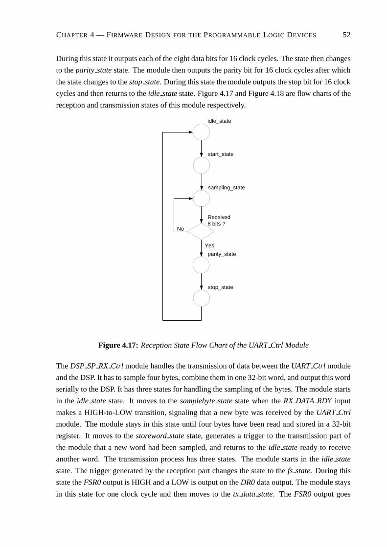
CHAPTER 4 — FIRMWARE DESIGN FOR THE PROGRAMMABLE LOGIC DEVICES 52
During this state it outputs each of the eight data bits for 16 clock cycles. The state then changes
to the parity state state. The module then outputs the parity bit for 16 clock cycles after which
the state changes to the stop state. During this state the module outputs the stop bit for 16 clock
cycles and then returns to the idle state state. Figure 4.17 and Figure 4.18 are flow charts of the
reception and transmission states of this module respectively.
Received8 bits ?
idle_state
start_state
sampling_state
parity_state
stop_state
No
Yes
Figure 4.17: Reception State Flow Chart of the UART Ctrl Module
The DSP SP RX Ctrl module handles the transmission of data between the UART Ctrl module
and the DSP. It has to sample four bytes, combine them in one 32-bit word, and output this word
serially to the DSP. It has three states for handling the sampling of the bytes. The module starts
in the idle state state. It moves to the samplebyte state state when the RX DATA RDY input
makes a HIGH-to-LOW transition, signaling that a new byte was received by the UART Ctrl
module. The module stays in this state until four bytes have been read and stored in a 32-bit
register. It moves to the storeword state state, generates a trigger to the transmission part of
the module that a new word had been sampled, and returns to the idle state ready to receive
another word. The transmission process has three states. The module starts in the idle state
state. The trigger generated by the reception part changes the state to the fs state. During this
state the FSR0 output is HIGH and a LOW is output on the DR0 data output. The module stays
in this state for one clock cycle and then moves to the tx data state. The FSR0 output goes

CHAPTER 4 — FIRMWARE DESIGN FOR THE PROGRAMMABLE LOGIC DEVICES 53
idle_state
start_state
tx_data_state
parity_state
stop_state
No
Yes
Transmitted8 bits ?
Figure 4.18: Transmission State Flow Chart of the UART Ctrl Module

CHAPTER 4 — FIRMWARE DESIGN FOR THE PROGRAMMABLE LOGIC DEVICES 54
LOW and for 32 clock cycles the module then outputs each of the 32 bits of the sampled word.
The module then returns to the idle state state. Figure 4.19 and Figure 4.20 are the flow charts
of the reception and transmission states of this module respectively.
Received4 bytes ?
idle_state
samplebyte_state
storeword_state
No
Yes
Figure 4.19: Reception State Flow Chart of the DSP SP RX Ctrl Module
Transmitted32 bits ?
idle_state
fs_state
tx_data_state
No
Yes
Figure 4.20: Transmission State Flow Chart of the DSP SP RX Ctrl Module
The DSP SP TX Ctrl module handles data transmission between the DSP and the UART Ctrl
module. It samples a byte from the serial data input received from the DSP, and outputs the byte
in parallel to the UART Ctrl module. It has four states for handling this process. The module
starts in the idle state state. It moves to the rx sampleword state state when the FSX0 input
makes a LOW-to-HIGH transition signalling that a new byte is to be transmitted by the DSP. The

CHAPTER 4 — FIRMWARE DESIGN FOR THE PROGRAMMABLE LOGIC DEVICES 55
module stays in this state until the eight bits of the byte have been read and stored in a register. It
then moves to the start tx state state, signals the UART Ctrl through its TX DATA RDY output
that new transmission data is ready, and moves to the wait data sent state state. It waits in this
state until the DATA SENT input makes a HIGH-to-LOW transition. The module then returns
to the idle state state. Figure 4.21 is a flow chart of the states of this module.
Received8 bits ?
idle_state
rx_sampleword_state
start_tx_state
No
Yes
ReceivedSent ?
No
Yes
wait_data_sent_state
Figure 4.21: State Flow Chart of the DSP SP TX Ctrl Module
4.2.4 The DSP Boot Controller
In this section the reset and boot procedure of the DSP is discussed. The module responsible
for these tasks is the DSP BOOT Ctrl module which is shown in Figure 4.22. The BOOT TYPE
input determines the origin of the boot data of the DSP. When this input is LOW, the system
boots the DSP from its serial port and when its HIGH, from flash RAM 0. The module has five
states. It starts in the state0 state. When the RESET input makes a HIGH-to-LOW transition,
it triggers the module to change its state to the state1 state. It stays in this state for 10 clock
cycles and then goes to the state2 state. The module stays for 50 clock cycles in this state during
which the output to the DSP reset input, the DSP nRESET output, is pulled LOW. The module
then moves to the state3 state where it stays for seven clock cycles. It then moves to the state4
state for one clock cycle. During this state the appropriate DSP external interrupt input is pulled

CHAPTER 4 — FIRMWARE DESIGN FOR THE PROGRAMMABLE LOGIC DEVICES 56
CLK
RESET
DSP_BOOT_Ctrl
nINT1
nINT3
DSP_nRESET
BOOT_TYPE
Figure 4.22: Diagram of the DSP BOOT Ctrl Module
LOW. For a serial boot, the nINT3 output is pulled LOW, while for a flash RAM boot, the nINT1
output is pulled LOW. The module then returns to the state0 state.
4.2.5 The Data Bus Access Controller
In this section the generation of the device select signals is discussed. The DEV SEL Ctrl is
responsible for this task. The DSP has a 24-bit address bus. This implies that it can address
16 million address spaces. The address map for the system is shown in Figure 3.9. From this
diagram it can be seen that the address space had been divided into 16 blocks of 1 million
address spaces. Each of the FPGAs, EPLDs, and flash RAMs had been assigned to one of these
blocks. The task of the DEV SEL Ctrl module is to send a chip select signal to the appropriate
device when the DSP accesses memory inside the block assigned to that device. The module
does that by examining the four most significant bits of the 24-bit address bus. By generating
a chip select signal in this way, it is not necessary to route all 24 of the address lines to all the
devices, but just enough to provide them with an address space that is big enough. The module
has a 4-bit address input, ADDR, that is connected to the 4 most significant address outputs of
the DSP and a chip select output for each of the devices assigned a memory block. The module
is shown in Figure 4.23.
CLK
RESET
DEV_SEL_Ctrl
FPGAMAIN_nCS
FPGANLG_nCS
FRAM0_nCS
FRAM1_nCS
ADDR
EXBUS0_nCS
EXBUS1_nCS
Figure 4.23: Diagram of the DEV SEL Ctrl Module
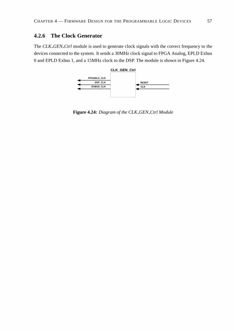
CHAPTER 4 — FIRMWARE DESIGN FOR THE PROGRAMMABLE LOGIC DEVICES 57
4.2.6 The Clock Generator
The CLK GEN Ctrl module is used to generate clock signals with the correct frequency to the
devices connected to the system. It sends a 30MHz clock signal to FPGA Analog, EPLD Exbus
0 and EPLD Exbus 1, and a 15MHz clock to the DSP. The module is shown in Figure 4.24.
CLK
RESET
CLK_GEN_Ctrl
FPGANLG_CLK
DSP_CLK
EXBUS_CLK
Figure 4.24: Diagram of the CLK GEN Ctrl Module

CHAPTER 4 — FIRMWARE DESIGN FOR THE PROGRAMMABLE LOGIC DEVICES 58
4.3 Design of the Firmware for FPGA Analog
In this section the firmware design for FPGA Analog, is discussed. In section 4.3.1, the imple-
mentation of the interrupt handler is discussed. In subsequent sections the implementation of
the ADC, DAC and LCD controllers and the implementation of the PWM outputs and PWM
error inputs are discussed.
4.3.1 The Processing of Interrupts
In this section the mechanism for generating interrupts to the DSP is discussed. The module
responsible for this task is Interrupt Ctrl. Figure 4.25 is a diagram of the interface of this
module. The Interrupt Ctrl module generates interrupts for external interrupt 0 and 2 of the
DSP. The sources for interrupt 0 are the ADCs, the keypad, and the status outputs of the two
pwm blocks. The sources for interrupt 2 are the PWM top and bottom error signals. The
INT EN IN input is from the interrupt enable register in the Data Ctrl module. Table 4.6 is the
definition of the interrupt enable register.
Bit Number Source of Interrupt
0 ADC 0 data ready
1 ADC 1 data ready
2 ADC 2 data ready
3 ADC 3 data ready
4 Keypressed on keypad
5 Error with a PWM TOP switch
6 Error with a PWM BOT switch
7 PWM block 0 COMPAREUP event
8 PWM block 0 COMPAREDOWN event
9 PWM block 0 RAMPDIR event
10 PWM block 0 COUNTERZERO event
11 PWM block 1 COMPAREUP event
12 PWM block 1 COMPAREDOWN event
13 PWM block 1 RAMPDIR event
14 PWM block 1 COUNTERZERO event
Table 4.6: The Definition of the Interrupt Enable Register
The INT REG is the output of a register representing the interrupts that had occurred. The
definition of this register is given by table 4.7.
The Interrupt 0 and 2 Sources inputs are interrupt inputs from all the different modules that

CHAPTER 4 — FIRMWARE DESIGN FOR THE PROGRAMMABLE LOGIC DEVICES 59
Bit Number Source of Interrupt
0 ADCs
1 Keypad
2 PWM TOP error
3 PWM BOT error
4 PWM block 0
5 PWM block 1
Table 4.7: The Definition of the Interrupt Register
generate interrupts for interrupt 0 and 2 respectively. The Interrupt 0 and 2 Sources outputs are
from registers containing the status of the interrupt sources and are connected to the DATA Ctrl
module. This enables the DSP to obtain more specific information on the source of an interrupt.
The INT0 OUT and INT2 OUT outputs directly drive the interrupt 0 and 2 inputs of the DSP.
Like in the other modules, the RESET input is used to reset the module and the CLK input is
the clock signal regulating the module.
CLK
RESET
Interrupt_Ctrl
Interrupt 0 sources
Interrupt 2 sources
INT2_OUT
INT0_OUT
INT_REG6
INT_EN_IN15
Interrupt 0 sources
Interrupt 2 sources
Figure 4.25: Diagram of the Interrupt Ctrl Module
4.3.2 The Control of the Analog-to-Digital Converters
In this section the control of the analog-to-digital converters is discussed. Interfacing to one
of the ADC’s involves writing configuration data serially to, and reading data serially from the
ADC. The main module controlling an ADC is ADC Ctrl. This module is connected directly to
the inputs and outputs of the ADC it controls. The other modules are ADC Chan Generator and
ADC Data Store. These modules are connected to ADC Ctrl, the former supplying the number
of the channel that has to be sampled next, and the latter receiving the most recent data sample.

CHAPTER 4 — FIRMWARE DESIGN FOR THE PROGRAMMABLE LOGIC DEVICES 60
ADC Data Store concatenates the sample’s channel number to the sample data, and outputs the
result. Each of the four ADC’s in the system is controlled by the combination of these three
modules, one for each ADC.
The ADC Controller
The ADC Ctrl module is the interface between an ADC and FPGA Analog. This module gen-
erates and sends the control signals to the ADC and receives the output data from the ADC.
Figure 4.26 is a schematic of the ADC Ctrl module. Table 4.8 lists the pins that are used in the
microcontroller mode to interface with the ADC.
Pin Name Pin Type Description
ADC SDOUT Input ADC serial data output
ADC SDIN Output ADC serial data input
ADC nCS Output ADC chip select
ADC SCLK Output ADC clock input
Table 4.8: The Interface of the ADC Ctrl Module to an ADC
The ADC SDOUT input receives the data sample serially from the ADC, while the ADC SDIN
output sends the configuration data to the ADC. ADC nCS is the active LOW chip select output
which activates the ADC’s interface pins. ADC SCLK is the clock output to the ADC which
controls the data transfer rate. One data transfer cycle is 16 bits long. During a transfer, the
16 configuration data bits for the next sampling operation are output to the ADC. During the
last 10 clock cycles, the 10 data bits representing the previously sampled data are received from
the ADC. Table 4.9 lists the pins that are used to interface with the rest of the logic in FPGA
Analog.
Pin Name Pin Type Description
ADC DATA Output Previous sampled data output
ADC DATA RDY Output New data ready flag
ADC CONF DATA Input Configuration data input
ADC CHAN Input Sampling channel number input
ADC nEN Input Module enable input
RESET Input Module reset input
CLK Input Module clock input
Table 4.9: The Interface of the ADC Ctrl Module to the Rest of FPGA Analog
ADC DATA is a 10 bit output representing the previously sampled data. The ADC DATA RDY
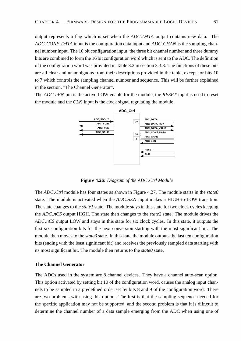
CHAPTER 4 — FIRMWARE DESIGN FOR THE PROGRAMMABLE LOGIC DEVICES 61
output represents a flag which is set when the ADC DATA output contains new data. The
ADC CONF DATA input is the configuration data input and ADC CHAN is the sampling chan-
nel number input. The 10 bit configuration input, the three bit channel number and three dummy
bits are combined to form the 16 bit configuration word which is sent to the ADC. The definition
of the configuration word was provided in Table 3.2 in section 3.3.3. The functions of these bits
are all clear and unambiguous from their descriptions provided in the table, except for bits 10
to 7 which controls the sampling channel number and sequence. This will be further explained
in the section, ”The Channel Generator”.
The ADC nEN pin is the active LOW enable for the module, the RESET input is used to reset
the module and the CLK input is the clock signal regulating the module.
ADC_DATA
ADC_DATA_RDY
ADC_CONF_DATA
ADC_CHAN
ADC_SDOUT
ADC_SDIN
ADC_nCS
ADC_SCLK
ADC_nEN
CLK
RESET
ADC_Ctrl
10
10
3
ADC_DATA_VALID
Figure 4.26: Diagram of the ADC Ctrl Module
The ADC Ctrl module has four states as shown in Figure 4.27. The module starts in the state0
state. The module is activated when the ADC nEN input makes a HIGH-to-LOW transition.
The state changes to the state1 state. The module stays in this state for two clock cycles keeping
the ADC nCS output HIGH. The state then changes to the state2 state. The module drives the
ADC nCS output LOW and stays in this state for six clock cycles. In this state, it outputs the
first six configuration bits for the next conversion starting with the most significant bit. The
module then moves to the state3 state. In this state the module outputs the last ten configuration
bits (ending with the least significant bit) and receives the previously sampled data starting with
its most significant bit. The module then returns to the state0 state.
The Channel Generator
The ADCs used in the system are 8 channel devices. They have a channel auto-scan option.
This option activated by setting bit 10 of the configuration word, causes the analog input chan-
nels to be sampled in a predefined order set by bits 8 and 9 of the configuration word. There
are two problems with using this option. The first is that the sampling sequence needed for
the specific application may not be supported, and the second problem is that it is difficult to
determine the channel number of a data sample emerging from the ADC when using one of
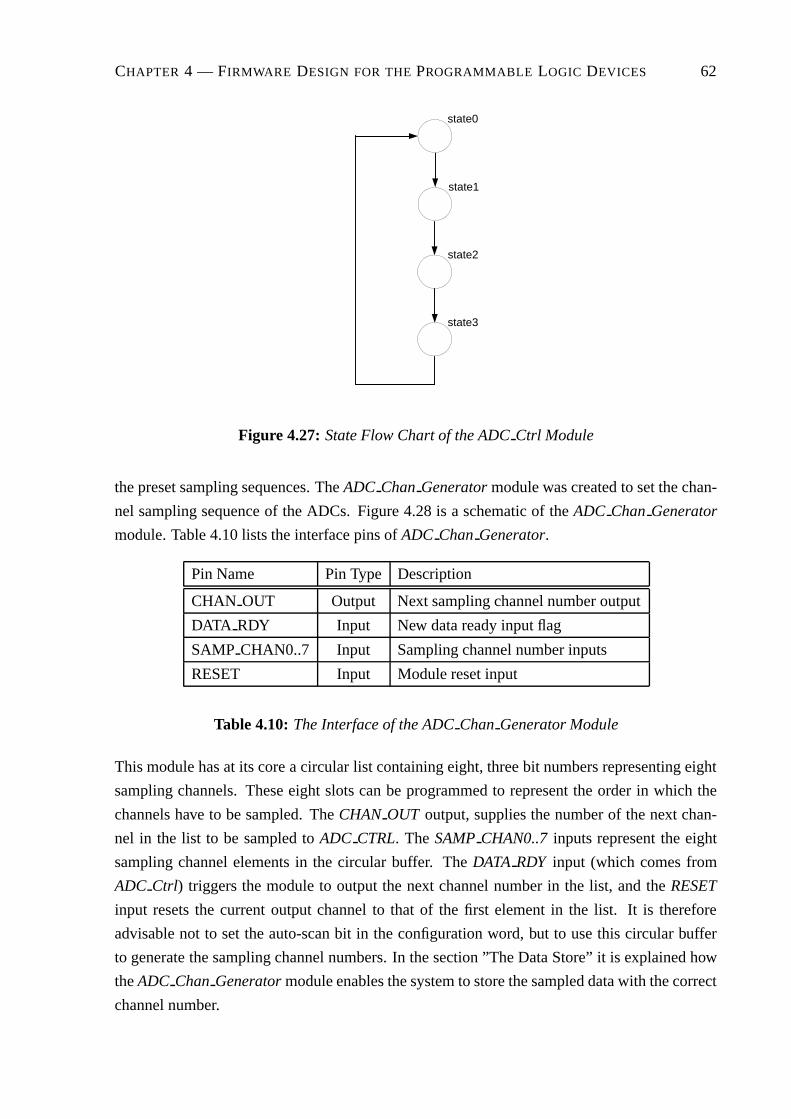
CHAPTER 4 — FIRMWARE DESIGN FOR THE PROGRAMMABLE LOGIC DEVICES 62
state0
state1
state2
state3
Figure 4.27: State Flow Chart of the ADC Ctrl Module
the preset sampling sequences. The ADC Chan Generator module was created to set the chan-
nel sampling sequence of the ADCs. Figure 4.28 is a schematic of the ADC Chan Generator
module. Table 4.10 lists the interface pins of ADC Chan Generator.
Pin Name Pin Type Description
CHAN OUT Output Next sampling channel number output
DATA RDY Input New data ready input flag
SAMP CHAN0..7 Input Sampling channel number inputs
RESET Input Module reset input
Table 4.10: The Interface of the ADC Chan Generator Module
This module has at its core a circular list containing eight, three bit numbers representing eight
sampling channels. These eight slots can be programmed to represent the order in which the
channels have to be sampled. The CHAN OUT output, supplies the number of the next chan-
nel in the list to be sampled to ADC CTRL. The SAMP CHAN0..7 inputs represent the eight
sampling channel elements in the circular buffer. The DATA RDY input (which comes from
ADC Ctrl) triggers the module to output the next channel number in the list, and the RESET
input resets the current output channel to that of the first element in the list. It is therefore
advisable not to set the auto-scan bit in the configuration word, but to use this circular buffer
to generate the sampling channel numbers. In the section ”The Data Store” it is explained how
the ADC Chan Generator module enables the system to store the sampled data with the correct
channel number.

CHAPTER 4 — FIRMWARE DESIGN FOR THE PROGRAMMABLE LOGIC DEVICES 63
DATA_RDY
CHAN_OUT SAMP_CHAN0
SAMP_CHAN1
SAMP_CHAN2
SAMP_CHAN3
SAMP_CHAN4
SAMP_CHAN5
SAMP_CHAN6
SAMP_CHAN7
ADC_Chan_Generator
RESET
3
3
3
3
3
3
3
3
3
Figure 4.28: Diagram of the ADC Chan Generator Module
The Data Store
When receiving data samples from the ADC, it is difficult to determine which one of the eight
channels it came from even if the sampling sequence is known. Part of the problem was fixed
by setting the sampling sequence with the ADC Chan Generator module. Even though this
meant that the possible sampling channel numbers are known, it still did not make it easier to
know from which ADC channel the current data sample came. The problem was solved by
creating the ADC Data Store module which concatenates the correct channel number output
from the ADC Chan Generator module to the sampled data before it is made available to the
rest of the system. Thus, a 13 bit word is created consisting of the 10 bit data sample and its
three bit channel number. Figure 4.29 is a schematic of the ADC Data Store module. Table
4.11 lists the interface pins of ADC Data Store. The module receives the new sample data
Pin Name Pin Type Description
DATA IN Input The new data sample input
CHAN IN Input The new sampling channel input
DATA RDY Input The new data flag input
DATA OUT Output Combination of the new data & sampling channel output
RESET Input Module reset input
Table 4.11: The Interface of the ADC Data Store Module
and channel numbers through the DATA IN and CHAN IN inputs respectively. The DATA RDY
input triggers the module to combine the DATA IN and CHAN IN inputs and output the result
at the DATA OUT output. The RESET input resets the module.

CHAPTER 4 — FIRMWARE DESIGN FOR THE PROGRAMMABLE LOGIC DEVICES 64
DATA_OUT
RESET
ADC_Data_Store
DATA_RDY
CHAN_IN
DATA_IN
3
1013
DATA_VALID
Figure 4.29: Diagram of the ADC Data Store Module
4.3.3 The Control of the Digital-to-Analog Converters
In this section the control of the digital-to-analog converters is discussed. The DAC Ctrl module
generates and sends the control signals to the DAC. Figure 4.30 is a schematic of the DAC Ctrl
module. Table 4.12 lists the pins that are used to interface with the DACs.
Pin Name Pin Type Description
DAC nSYNC Output DAC input data frame synchronization signal
DAC SCLK Output DAC serial clock input
DAC SDIN Output DAC serial data input
DAC nLDAC Output Simultaneous updating of both DAC outputs
Table 4.12: The Interface of the DAC Ctrl Module to a DAC
The DAC nSYNC output is the input data frame synchronization signal. When it goes LOW, it
powers the serial clock and data buffers, and enables the input shift register. Input data is then
transferred through the DAC SDIN output to the DAC on the falling edges of the next 16 clocks
transferred through the DAC SCLK output. If DAC nSYNC goes HIGH before the 16th falling
edge, the data transfer is aborted and ignored. Table 4.13 lists the pins that are used to interface
the rest of the system to DAC Ctrl. The DAC nLOAD input triggers the transfer of the relevant
DAC’s data. The DAC CTRL DATA input determines which one (or both) of the DACs will be
updated when the load trigger occurs. The DAC X DATA input is the data that is going to be
transferred to DAC X if it was selected to be updated. The DAC X CONF DATA corresponds
to bits 12 to 14 of the DAC configuration bits as was defined in table 3.3 in section 3.3.4. As in
the other modules, the RESET input is used to reset the module and the CLK input is the clock
signal regulating the module.
The DAC Ctrl module has six states as shown in Figure 4.31. It starts in the state0 state. The
HIGH-to-LOW transition of the DAC nLOAD input is the signal that the DACs have to be
updated and the state changes to the state1 state. The module stays in this state for four clock
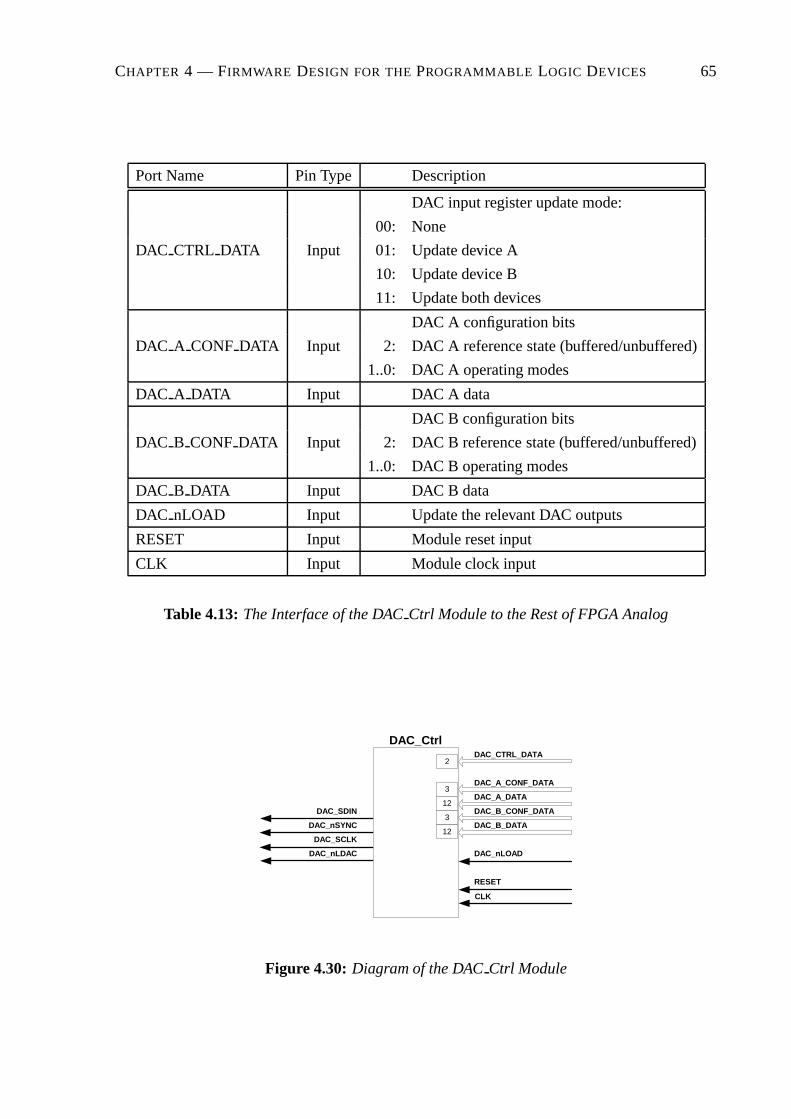
CHAPTER 4 — FIRMWARE DESIGN FOR THE PROGRAMMABLE LOGIC DEVICES 65
Port Name Pin Type Description
DAC input register update mode:
00: None
DAC CTRL DATA Input 01: Update device A
10: Update device B
11: Update both devices
DAC A configuration bits
DAC A CONF DATA Input 2: DAC A reference state (buffered/unbuffered)
1..0: DAC A operating modes
DAC A DATA Input DAC A data
DAC B configuration bits
DAC B CONF DATA Input 2: DAC B reference state (buffered/unbuffered)
1..0: DAC B operating modes
DAC B DATA Input DAC B data
DAC nLOAD Input Update the relevant DAC outputs
RESET Input Module reset input
CLK Input Module clock input
Table 4.13: The Interface of the DAC Ctrl Module to the Rest of FPGA Analog
DAC_CTRL_DATA
DAC_nLOAD
DAC_A_CONF_DATA
DAC_A_DATA
DAC_SDIN
DAC_nSYNC
DAC_SCLK
DAC_nLDAC
CLK
RESET
DAC_Ctrl
2
3
12DAC_B_CONF_DATA
DAC_B_DATA3
12
Figure 4.30: Diagram of the DAC Ctrl Module

CHAPTER 4 — FIRMWARE DESIGN FOR THE PROGRAMMABLE LOGIC DEVICES 66
cycles, keeping the DAC nSYNC output HIGH. The state then either changes to the state0,
state2 or state4 state depending on the DAC CTRL DATA input that determines which of the
DACs are to be updated (if any). Table 4.13 shows the possible values of this input and which
of the DACs are updated for each setting. When it has a value of ”00”, it implies that none of the
DACs must be updated, and the state changes to the state0 state. When it has a value of ”10”,
DAC B have to be updated and the state changes to state4. When it has either of the remaining
two values (”01” or ”11”), the state changes to state2. The module stays for 15 clock cycles
in states state2 and state4, driving the DAC nSYNC output LOW and sending the new data to
the input registers of the DACs. DAC A’s register is updated when the module is in state2 and
DAC B’s register in state4. When the module is in state2 and only DAC A must be updated, or
in state4, the state changes to state5. If it was in state2 and both DACs have to be updated, the
state changes to state3. States state1 and state3 have the same function. They must ensure that
the nSYNC input of the DAC is driven HIGH for the correct period after one transaction ends
and before the next one can begin. After four clock cycles the state changes to the state5 state.
During this state that takes two clock cycles to complete, the DAC nLDAC output is driven
LOW, signaling the DACs to update their outputs. The state the changes to state0.
4.3.4 The Pulse-Width Modulation Interface
In this section the control of the pulse-width modulation interface is discussed. The PWM
interface is controlled by the PWM Ctrl module shown in Figure 4.32. It has four pairs of
outputs and error signal inputs. The operation of the module is enabled with the PWM nEN
input. Also shown in the diagram is the configuration inputs for the module. In this PWM
implementation, the core of the module is a triangular wave. It is generated by incrementing an
internal variable from zero to its maximum value, given by the TRIMAX input and then back
down to zero. The internal clock signal driving the module is a lower frequency version of the
system clock signal, CLK. The TRIFREQSCALE input determines the amount of delay. Eq.4.1
is the equation for determining the internal clock frequency of the module.
������ �
��� � �� �!"�� �!�(4.1)
where
������ is the resultant internal clock frequency,
is the input clock frequency, and
�� �!"�� �! is the internal clock frequency delay input parameter.The values of the TRIMAX and TRIFREQSCALE variables determine the switching frequency
of the PWM outputs. Eq.4.2 is the equation for calculating the switching frequency using these
input parameters.
! � ������
���� � #�

CHAPTER 4 — FIRMWARE DESIGN FOR THE PROGRAMMABLE LOGIC DEVICES 67
Control Data = "00"
state0
state1
state3
Yes
No
state4
Control Data = "01" or "11"
Yes
No
state2
Control Data = "01"
No
Yes
state5
Figure 4.31: State Flow Chart of the DAC Ctrl Module
CHAPTER 4 — FIRMWARE DESIGN FOR THE PROGRAMMABLE LOGIC DEVICES 68
�
����� � �� �!"�� �!������� � #�(4.2)
where
! is the switching frequency,
������ is the internal clock frequency,
is the input clock frequency,
�� � # is the maximum value of the triangular waveform, and
�� �!"�� �! is the clock delay input parameter.The module also has four reference inputs REFA, REFB, REFC and REFN, one for each of
the output pairs. These input values are independently compared to the generated triangular
waveform to determine which one of the two outputs in a pair should be ON (and the other OFF).
The DEADTIME input determines the amount of time (which is called deadtime) between the
switching OFF of the one switch and the switching ON of the other switch in the pair. Deadtime
is necessary, because if both the switches are ON at the same time, the DC bus of the inverter
containing the switches, will be shorted. Eq.4.3 is the equation for calculating the resultant
deadtime applied to the PWM outputs.
��������� � � ����� � �� �!"�� �!���! �� �!� (4.3)
where
��������� is the deadtime in seconds,
� is the period of the input clock in seconds,
�! �� �! is the deadtime input parameter, and
�� �!"�� �! is the clock delay input parameter.The COMPAREUPVAL input is compared to the triangular waveform while its incrementing,
and the COMPAREDOWNVAL input is compared when it is decrementing. When the triangular
wave counter is incrementing and the COMPAREUPVAL parameter is equal to the value of the
triangular wave counter, the COMPAREUP output is driven HIGH. When the triangular wave
counter is decrementing and the COMPAREDOWNVAL parameter is equal to the value of the
triangular wave counter, the COMPAREDOWN output is driven HIGH. These two status outputs
COMPAREUP and COMPAREDOWN can therefore be used to mark a certain time instance
relative to the start of the switching period. Both these outputs are reset when a new switching
period starts. Another status output of the module is the RAMPDIR output. It is driven HIGH
when the triangular wave counter is incrementing and LOW when it is decrementing. The fourth
and final status output is the COUNTERZERO output. It is driven HIGH when the triangular
wave counter is zero and is LOW when it is non-zero. Like in the other modules, the RESET
input is used to reset the module.
Each of the four switching pairs is controlled by its own state-machine. Figure 4.33 is a flow
chart of this state-machine. The state-machine starts in the topsstate state. In this state the TOP
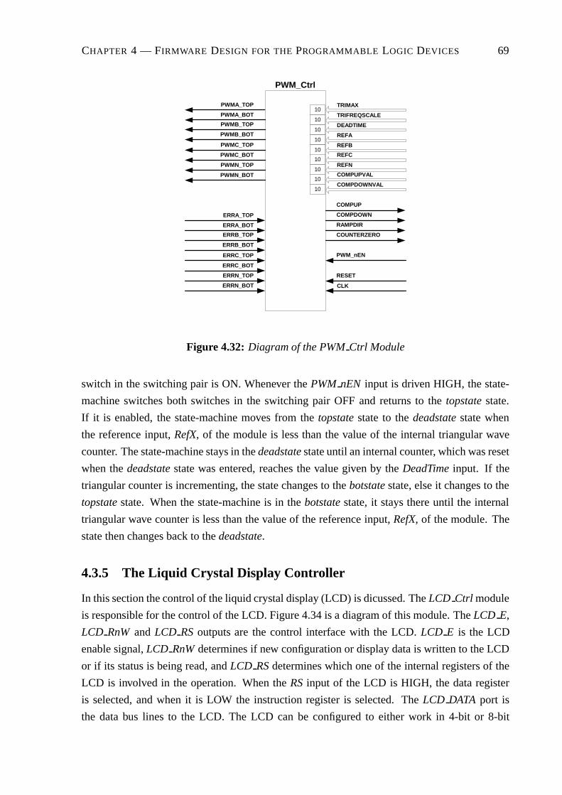
CHAPTER 4 — FIRMWARE DESIGN FOR THE PROGRAMMABLE LOGIC DEVICES 69
COMPUP
TRIMAX
TRIFREQSCALE
PWMA_TOP
CLK
RESET
PWM_Ctrl
10
10DEADTIME
REFA10
10
PWMA_BOT
PWMB_TOP
PWMB_BOT
PWMC_TOP
PWMC_BOT
PWMN_TOP
PWMN_BOT
ERRA_TOP
ERRA_BOT
ERRB_TOP
ERRB_BOT
ERRC_TOP
ERRC_BOT
ERRN_TOP
ERRN_BOT
REFB10
REFC10
REFN10
COMPUPVAL10
COMPDOWNVAL10
COMPDOWN
RAMPDIR
COUNTERZERO
PWM_nEN
Figure 4.32: Diagram of the PWM Ctrl Module
switch in the switching pair is ON. Whenever the PWM nEN input is driven HIGH, the state-
machine switches both switches in the switching pair OFF and returns to the topstate state.
If it is enabled, the state-machine moves from the topstate state to the deadstate state when
the reference input, RefX, of the module is less than the value of the internal triangular wave
counter. The state-machine stays in the deadstate state until an internal counter, which was reset
when the deadstate state was entered, reaches the value given by the DeadTime input. If the
triangular counter is incrementing, the state changes to the botstate state, else it changes to the
topstate state. When the state-machine is in the botstate state, it stays there until the internal
triangular wave counter is less than the value of the reference input, RefX, of the module. The
state then changes back to the deadstate.
4.3.5 The Liquid Crystal Display Controller
In this section the control of the liquid crystal display (LCD) is dicussed. The LCD Ctrl module
is responsible for the control of the LCD. Figure 4.34 is a diagram of this module. The LCD E,
LCD RnW and LCD RS outputs are the control interface with the LCD. LCD E is the LCD
enable signal, LCD RnW determines if new configuration or display data is written to the LCD
or if its status is being read, and LCD RS determines which one of the internal registers of the
LCD is involved in the operation. When the RS input of the LCD is HIGH, the data register
is selected, and when it is LOW the instruction register is selected. The LCD DATA port is
the data bus lines to the LCD. The LCD can be configured to either work in 4-bit or 8-bit

CHAPTER 4 — FIRMWARE DESIGN FOR THE PROGRAMMABLE LOGIC DEVICES 70
botstate
PWM blockenabled ?
topstate
deadstate
No
Yes
Ramp counter < ref XYes
No
Dead time counter < DeadTime inputANDRampDir = '1'
No
Yes
RampDir = '1'
Yes
PWM blockenabled ?
No
Yes
Ramp counter > ref XYes
No
Dead time counter < DeadTime inputANDRampDir = '0'
Yes
No
RampDir = '0'
Yes
No
PWM blockenabled ?
No
Yes
No
Figure 4.33: State Flow Chart of the PWM Ctrl Module

CHAPTER 4 — FIRMWARE DESIGN FOR THE PROGRAMMABLE LOGIC DEVICES 71
mode. In this application it was configured for 8-bit operation. The remaining ports are used
to interface the module with the rest of the FPGA Analog system. The LCD MODE DATA
input is the configuration data input for the module. When the LCD UPDATE MODE input is
pulsed LOW, this configuration data is sent to the LCD. The LCD CHAR input is the character
to be displayed on the LCD at the position given by the address input, LCD ADDR, when the
LCD UPDATE DATA input is pulsed LOW. The LCD RESET input causes the LCD to be reset
and reconfigured. The RESET input resets the module and the CLK input is the clock input to
the module.
LCD_DATA
LCD_UPDATE_MODE
LCD_MODE_DATA
LCD_E
LCD_RnW
LCD_RS
CLK
RESET
LCD_Ctrl
8 8LCD_CHAR
LCD_ADDR8
7
LCD_UPDATE_DATA
LCD_RESET
LCD_RDYnBSY
Figure 4.34: Diagram of the LCD Ctrl Module
The LCD Ctrl module has four interdependent state-machines. The first state-machine, the
lcd state state-machine, determines the data type to be transferred to the LCD. Figure 4.35 is
a flow chart of the lcd state state-machine. The LCD starts in the idle state state. When the
LCD RESET input is pulsed LOW, the lcd state changes to the reset state state. When the
LCD UPDATE MODE input is pulsed LOW, the state changes to the modestate state and when
the LCD UPDATE DATA input is pulsed LOW, the state changes to the datastate state. The
module stays in these three states until the next state-machine, the data state state-machine, is
in the nodatastate state and then returns to the idlestate state.
The data state state-machine determines the data to be transferred to the LCD. Figure 4.36 is a
flow chart of the data state state-machine. When the state of the lcd state state-machine moves
from the idle state, it triggers the data state state-machine to move to its next state. When
the state of the lcd state state-machine is modedatastate state, the state-machine moves to the
modedatastate state. When the lcd state state-machine is in the datastate state, the data state
state-machine moves to the addrstate state and it moves to the def0state when the lcd state
state-machine is in the resetstate state. When in the modedatastate state, the module outputs
the data on the LCD MODE DATA input to the LCD. This data changes the mode of the LCD.
The data state state-machine then returns to the nodatastate. When in the addrstate state,
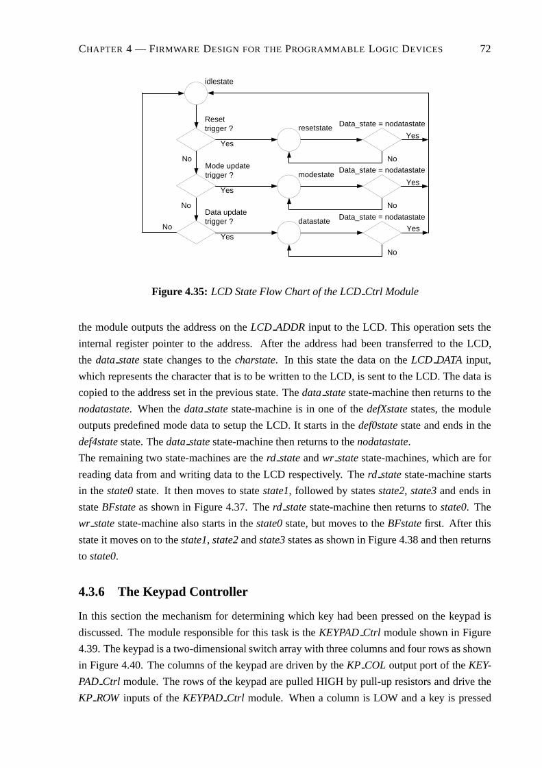
CHAPTER 4 — FIRMWARE DESIGN FOR THE PROGRAMMABLE LOGIC DEVICES 72
Resettrigger ?
idlestate
resetstate
NoMode updatetrigger ?
NoData updatetrigger ?
No
Data_state = nodatastate
Yes
No
Yes
No
Yes
No
modestate
datastate
Yes
Yes
Yes
Data_state = nodatastate
Data_state = nodatastate
Figure 4.35: LCD State Flow Chart of the LCD Ctrl Module
the module outputs the address on the LCD ADDR input to the LCD. This operation sets the
internal register pointer to the address. After the address had been transferred to the LCD,
the data state state changes to the charstate. In this state the data on the LCD DATA input,
which represents the character that is to be written to the LCD, is sent to the LCD. The data is
copied to the address set in the previous state. The data state state-machine then returns to the
nodatastate. When the data state state-machine is in one of the defXstate states, the module
outputs predefined mode data to setup the LCD. It starts in the def0state state and ends in the
def4state state. The data state state-machine then returns to the nodatastate.
The remaining two state-machines are the rd state and wr state state-machines, which are for
reading data from and writing data to the LCD respectively. The rd state state-machine starts
in the state0 state. It then moves to state state1, followed by states state2, state3 and ends in
state BFstate as shown in Figure 4.37. The rd state state-machine then returns to state0. The
wr state state-machine also starts in the state0 state, but moves to the BFstate first. After this
state it moves on to the state1, state2 and state3 states as shown in Figure 4.38 and then returns
to state0.
4.3.6 The Keypad Controller
In this section the mechanism for determining which key had been pressed on the keypad is
discussed. The module responsible for this task is the KEYPAD Ctrl module shown in Figure
4.39. The keypad is a two-dimensional switch array with three columns and four rows as shown
in Figure 4.40. The columns of the keypad are driven by the KP COL output port of the KEY-
PAD Ctrl module. The rows of the keypad are pulled HIGH by pull-up resistors and drive the
KP ROW inputs of the KEYPAD Ctrl module. When a column is LOW and a key is pressed

CHAPTER 4 — FIRMWARE DESIGN FOR THE PROGRAMMABLE LOGIC DEVICES 73
LCD_state = modestate ?
nodatastate
No
LCD_state = datastate ?
No
LCD_state = resetstate ?No
def0state
Yes
Yes
Yes
def1state
def2state
def3state
def4state
addrstate
charstate
modedatastate
Figure 4.36: Data State Flow Chart of the LCD Ctrl Module
State Required Clock Cycles Time in
Time in State State
state0 NA NA NA
state1 40ns 2 66.6ns
state2 220ns 7 233.3ns
state3 280ns 9 300ns
BFstate $46�s 1500 50�s
Table 4.14: The Duration of each wr state and rd state State-Machine State

CHAPTER 4 — FIRMWARE DESIGN FOR THE PROGRAMMABLE LOGIC DEVICES 74
state0
state1
state2
state3
BFstate
Figure 4.37: Read State Flow Chart of the LCD Ctrl Module
state0
state1
state2
state3
BFstate
Figure 4.38: Write State Flow Chart of the LCD Ctrl Module

CHAPTER 4 — FIRMWARE DESIGN FOR THE PROGRAMMABLE LOGIC DEVICES 75
CLK
RESET
Keypad_Ctrl
KP_COL KEYVAL4
KP_ROW3
4
Figure 4.39: Diagram of the KEYPAD Ctrl Module
in that column, the row in which the key is situated is driven LOW too. Therefore, the column
inputs of the keypad were driven in the following cyclical sequence:
...110� 101� 011� 111...
By monitoring the row outputs of the keypad, it is possible to determine which key was pressed
(if any), and output its value through the KEYVAL output port of the KEYPAD Ctrl. Table 4.15
lists the values of the rows and columns, the keys that they represent and the corresponding
KEYVAL output values.
Key Column Row KEYVAL
Value Value Output
’1’ 110 0111 1
’2’ 101 0111 2
’3’ 011 0111 3
’4’ 110 1011 4
’5’ 101 1011 5
’6’ 011 1011 6
’7’ 110 1101 7
’8’ 101 1101 8
’9’ 011 1101 9
’*’ 110 1011 11
’0’ 101 1011 10
’#’ 011 1011 12
Table 4.15: The Encoding of the Keypad

CHAPTER 4 — FIRMWARE DESIGN FOR THE PROGRAMMABLE LOGIC DEVICES 76
Row 0
Row 1
Row 2
Row 3
Co
lum
n 0
Co
lum
n 1
Co
lum
n 2
1 2 3
4 5 6
7 8 9
0 #*
Figure 4.40: Diagram of the Switch Configuration of the Keypad

CHAPTER 4 — FIRMWARE DESIGN FOR THE PROGRAMMABLE LOGIC DEVICES 77
4.4 Design of the Firmware for EPLD ExBus
In this section the firmware design for the EPLDs is discussed. The main function of the EPLDs
is to provide the interface between the DSP and the two expansion busses. Each of the EPLDs
controls one of the expansion busses. The physical layout of the two EPLD expansion bus
systems was done exactly the same. This implies that the same firmware design can be loaded
on both the EPLDs without the need to make changes to pin assignments before loading the
firmware to the two EPLDs.
4.4.1 The Complete Expansion Bus Module
The module implemented in the EPLDs is the EXBUS Single Complete module. This module
is shown in Figure 4.41. Its interface with the expansion bus consists of the following. It has
EXBUS
RDYnBSY
DATA
A_nEN
D_nEN
nACK
CLK
nRESET
ExBus_Single_Complete
n nADDR
n
nINT
nINTREQ_OUT
nCS
RnW
nINTREQ_IN
DSP_RnW
DSP_nSTRB
Figure 4.41: Diagram of the ExBus Single Complete Module
a bidirection bus, EXBUS, for the transfer of data and addresses. The interface has five control
lines. The A nEN and D nEN outputs signal whether the data on the expansion bus is an address
or the data that has to be transferred. The RnW output indicates whether it is a read or a write
transaction that is being processed. The external device connected to the expansion bus signals
the module with the nACK input when it had processed the data on the bus. It can also send an
interrupt request with the nINTREQ IN to the module.
The module’s interface with the DSP consists of the following. It has a bidirectional bus, DATA,
that connects directly to the system data bus. There is also a 16-bit input, ADDR, which is
connected to the system address bus. The DSP RnW and DSP nSTRB inputs are the DSP’s
transaction type (read or write) and data bus strobe signals.
The module receives a chip select signal from FPGA Main through the nCS input. This input is
activated when the address on the address bus is in the range assigned to the specific expansion

CHAPTER 4 — FIRMWARE DESIGN FOR THE PROGRAMMABLE LOGIC DEVICES 78
bus. The module sends three control signals back to FPGA Main. The RDYnBSY output indi-
cates whether the module is ready for a new transaction or is still busy processing a previous
one. The nINT output is pulsed when the expansion port receives data from the external device
connected to it. This signal can then be used by FPGA Main to trigger the DSP to read the
new data from the expansion port module. The module outputs the interrupt received from the
nINTREQ IN input, to FPGA Main through the nINTREQ OUT output. The module receives
its global clock signal of 30MHz from FPGA Main through the CLK input. FPGA Main can
reset the module through the nRESET input. Figure 4.42 is a diagram of the modules used to
construct the ExBus Single Complete module. It can be seen in the diagram that the module is
EXBUS_IN
RDYnBSY
DATA_OUT
A_nEN
D_nEN
nACK
CLK
RESET
ExBus_Ctrl
n n
ADDRn
nINT
nCS
EXBUS_RnW
DSP_RnW
DSP_nSTRB
EXBUS_OUTn
RnW
nDATA_IN
IN_DATA
RnW CLK
Bidir
nBIDIR
nOUT_DATA
n
DSP_RnW
DATA
IN_DATA
RnW
Bidir
nBIDIR
nOUT_DATA
n
CLK
A_nEN
D_nEN
nACK
RnW
ADDR
nRESET
CLK
RDYnBSY
nINT
EXBUS
nCS
nINTREQ_IN nINTREQ_OUT
DSP_nSTRB
ExBus_Single_Complete
Figure 4.42: Diagram of the Components of the ExBus Single Complete Module
constructed using only two types of modules. The Bidir module is the same as the ones used
in FPGA Main and FPGA Analog. It is used to handle the transfer of data to and from the two
bidirectional busses, DATA and EXBUS. For a more detailled explanation refer to section 4.1.1.
The other module, ExBus Ctrl, is used to implement the data transfer protocol of the expansion
bus.
4.4.2 The Expansion Bus Control Module
The module implementing the data transfer protocol of the expansion busses, is the ExBus Ctrl
module. Figure 4.43 is a flow chart of the states of the module. The module starts in the
idle state state. When new data is placed on the DATA bus addressed to the specific expansion
bus, the data is latched and the module’s state changes to the addr state state. The module
stays in this state for four clock cycles and then moves to the addr ack state state. During
these two states the module outputs the address of the data on EXBUS. In the addr ack state

CHAPTER 4 — FIRMWARE DESIGN FOR THE PROGRAMMABLE LOGIC DEVICES 79
idle_state
addr_state
data_ack_state
nint_state
ReceivedAddress ?
Yes
No
data_state
ReceivedData ?
No
Yes
addr_ack_state
RnW = '1'
No
Yes
Figure 4.43: State Flow Chart of the ExBus Ctrl Module

CHAPTER 4 — FIRMWARE DESIGN FOR THE PROGRAMMABLE LOGIC DEVICES 80
state the module waits for a signal from the external device connected to the expansion port,
indicating that it received the address. This signal is received through the nACK input. When the
acknowledgement signal is received, the module moves to the data state state. If the signal was
not received after 14 clock cycles, the module returns to the idle state state. The module stays
for four clock cycles in the data state state and then moves to the data ack state state. During
these last two states the module outputs the data on EXBUS. It waits in the data ack state state
for the acknowledgement signal from the external device that it received the data. The signal
is again received through the nACK input. When the acknowledgement signal is received and
the transaction was for a read operation, the module moves to the nint state state. If either the
acknowledgement was not received after 14 clock cycles, or it was received and the transaction
was for a write operation, the module moves to the idle state state. In the nint state state, the
module outputs an interrupt pulse to FPGA Main through the nINT output and returns to the
idle state state.
This chapter discussed the design of the firmware for the four programmable logic devices
included in the system. The PEC33 system was tested by implementing a shunt active power
filter. The theory behind the implementation, simulation results obtained with the Simplorer
simulation software package and the practical results obtained is discussed in the next chapter.
Chapter 5
Test Implementation: Control of an Active
Power Filter
In this chapter the operation of the controller is tested by implementing a shunt active power
filter. The first section provides an overview of the system that was implemented. In subsequent
sections the basic compensation scheme and the theory behind it is explained, and the simulation
model and practical implementation of the system are discussed.
5.1 Overview of the System
In Figure 5.1 a simplified block diagram of the system is shown. The system consists of three
parts: the plant, the active power filter and the controller. The plant of the system is a three-phase
voltage source driving a three-phase rectifier connected to the series combination of an inductor
and a resistor. The load draws both real and reactive power from the source. The idea is that the
filter should inject current in such a way into the system, that the reactive power supplied to the
load, should come from the filter and not from the three-phase source. To achieve this the filter
is constructed using three phase arms (one for each phase of the plant) connected to three filter
inductors. The phase-arms control the current injected into the system through the inductors by
controlling the average voltage across the inductors. The final part of the system is the power
electronics controller that was developed, the PEC33. It measures the three phase currents, the
voltages supplied to the three phase rectifier and the current injected into the system by the three
phase arms. The PEC33 uses these values to calculate the control signals for the phase arms.
The phase arms are switched using space vector pulse-width modulation (SVPWM).
5.2 Theory of the Compensation Scheme
The first subsection provides an overview of the complete control scheme and in the subsequent
subsections detailed explanations of the instantaneous reactive power theory and the space
81
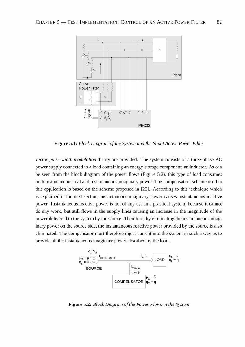
CHAPTER 5 — TEST IMPLEMENTATION: CONTROL OF AN ACTIVE POWER FILTER 82
Plant
ActivePower Filter
PEC33
Con
trol
Sig
nals
I_co
nvA
I_co
nvB
I_co
nvC
VA
VB
VC I A I B I C
Van
Vbn
Vcn
n
Figure 5.1: Block Diagram of the System and the Shunt Active Power Filter
vector pulse-width modulation theory are provided. The system consists of a three-phase AC
power supply connected to a load containing an energy storage component, an inductor. As can
be seen from the block diagram of the power flows (Figure 5.2), this type of load consumes
both instantaneous real and instantaneous imaginary power. The compensation scheme used in
this application is based on the scheme proposed in [22]. According to this technique which
is explained in the next section, instantaneous imaginary power causes instantaneous reactive
power. Instantaneous reactive power is not of any use in a practical system, because it cannot
do any work, but still flows in the supply lines causing an increase in the magnitude of the
power delivered to the system by the source. Therefore, by eliminating the instantaneous imag-
inary power on the source side, the instantaneous reactive power provided by the source is also
eliminated. The compensator must therefore inject current into the system in such a way as to
provide all the instantaneous imaginary power absorbed by the load.
LOAD
COMPENSATOR
pS = pqS = 0
pC = pqC = q
pL = pqL = q
Iconv_αIconv_β
Iα, Iβ
Vα, VβIsrc_α, Isrc_β
SOURCE
~
_
Figure 5.2: Block Diagram of the Power Flows in the System

CHAPTER 5 — TEST IMPLEMENTATION: CONTROL OF AN ACTIVE POWER FILTER 83
5.2.1 Overview of the Control Scheme
In this section the control strategy and the theory behind it is discussed. In the next two sub-
sections the instantaneous reactive power and the space vector pulse-width modulation theories
will be examined.
The inverter’s outputs are controlled using space vector pulse-width modulation. In Figure
5.4 a flow chart shows the various stages of the control scheme. After all the devices of the
controller involved in this application have been set up (which also involves enabling the ADCs
and the PWM control module), the processor waits for the Compare Down Value trigger. It is
set to be activated as close as possible to the end of the PWM switching cycle. This causes the
processor to stop sampling the input channels, and start calculating the PWM references for the
next cycle. The only other event which can interrupt the processor at this stage is a New Data
Sampled trigger. This trigger is activated when a new analog measurement has been sampled.
The processor then reads this data sample from FPGA Analog and stores the result. When the
controller receives the Compare Down Value trigger, it disables the New Data Sampled trigger
and starts calculating the PWM references. In Figure 5.5 the algorithm for calculating the
references is shown. As a first step (depicted by the C blocks), the measurements are converted
to their two phase equivalents in the �-� plane, using the Clarke transform (eq. 5.4). Conversion
of the %-�-& coordinates to the �-� plane makes the space vector theory easier to implement.
Next (in block B), using the transformed values of the currents and voltages supplied to the
three phase rectifier, the reference current which is to be supplied by the inverter during the next
PWM cycle is calculated, using the instantaneous reactive power compensation theory. This
process is discussed in section 5.2.2. The current injected into each phase of the system by the
inverter flows through an inductor. The voltage across an inductor is given by the following
equation:
'" � ��(
��(5.1)
The current flowing through the inductors and which is injected into the system is therefore a
function of the average output voltage of each arm of the inverter.
��"� � �� ����# � �$ � �
����# � ���#�!
(5.2)
where ��"� is the average voltage across the filter inductor of the phase,�� �
���# is the average output voltage reference,
�$ is the supply voltage measurement,
� is the inductance of the filter inductors,
����# is the converter current reference,
���# is the converter current measurement, and
�� is the switching period.Figure 5.3 is a diagram of one of the phases showing the currents and voltages used to calculate
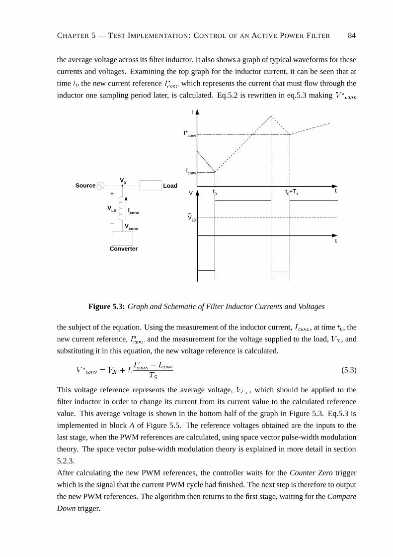
CHAPTER 5 — TEST IMPLEMENTATION: CONTROL OF AN ACTIVE POWER FILTER 84
the average voltage across its filter inductor. It also shows a graph of typical waveforms for these
currents and voltages. Examining the top graph for the inductor current, it can be seen that at
time �� the new current reference ����# which represents the current that must flow through the
inductor one sampling period later, is calculated. Eq.5.2 is rewritten in eq.5.3 making �� ����#
Converter
Source Load
Iconv
Vconv
VX
+
VLX
_
I*conv
Iconv
t0 t0+Tst
I
V
VLX
t
Figure 5.3: Graph and Schematic of Filter Inductor Currents and Voltages
the subject of the equation. Using the measurement of the inductor current, ���#, at time ��, the
new current reference, ����# and the measurement for the voltage supplied to the load, �$ , and
substituting it in this equation, the new voltage reference is calculated.
�� ����# � �$ � �
����# � ���#�!
(5.3)
This voltage reference represents the average voltage, ��"� , which should be applied to the
filter inductor in order to change its current from its current value to the calculated reference
value. This average voltage is shown in the bottom half of the graph in Figure 5.3. Eq.5.3 is
implemented in block A of Figure 5.5. The reference voltages obtained are the inputs to the
last stage, when the PWM references are calculated, using space vector pulse-width modulation
theory. The space vector pulse-width modulation theory is explained in more detail in section
5.2.3.
After calculating the new PWM references, the controller waits for the Counter Zero trigger
which is the signal that the current PWM cycle had finished. The next step is therefore to output
the new PWM references. The algorithm then returns to the first stage, waiting for the Compare
Down trigger.

CHAPTER 5 — TEST IMPLEMENTATION: CONTROL OF AN ACTIVE POWER FILTER 85
Compare DownTrigger ?
ProcessSamples
Calculate NewPWM References
Counter ZeroTrigger ?
UpdatePWM References
Yes
Yes
No
No
New DataSampled ?
No
Yes
Set up theController
Figure 5.4: Flow Chart of the Control Algorithm
IaIbIcVaVbVc
C[ ]
C[ ]
Iconv_aIconv_bIconv_c
C[ ]
B
A
Iα
Iβ
Vα
Vβ
Iconv_αIconv_β
I*conv_α
I*conv_β
V*conv_α
V*conv_βSVPWM
RefARefBRefC
Figure 5.5: Block Diagram of the Calculation of the PWM Reference Values

CHAPTER 5 — TEST IMPLEMENTATION: CONTROL OF AN ACTIVE POWER FILTER 86
Figure 5.6 is a graph of the signals involved in the pulse-width modulation process. The fre-
quency of the triangular waveform determines the switching frequency and is given by eq.4.2.
In this application the frequency scale factor was set to one and the maximum value for the
triangular wave to 750, which gave the desired switching frequecy of 5kHz. Also shown on
the graph are the Switching and the Compare Down references respectively. The switching
reference is the reference value for one of the switch pairs. The references for the other two
pairs were not included in the graph for clarity. The latter is a value which triggers the Compare
Down event. This value should be great enough to allow ample time to enable the measurements
to be taken and the references to be calculated (for the next PWM cycle).
TOP
BOTTOM
Counter ZeroTrigger
Compare DownTrigger
SwitchingReference
Compare DownReference
TStcdt1 t2 t
Figure 5.6: Graph of the Timing of the PWM Reference Signals
5.2.2 Instantaneous Reactive Power Theory
In this section some important concepts in reactive power theory are explained. In the next
section space vector pulse-width modulation will be examined.
Three phase voltages and currents can be expressed as vectors in a two dimensional %-�-& coor-
dinate system. The three vectors are separated from each other by ���Æ and can be transformed

CHAPTER 5 — TEST IMPLEMENTATION: CONTROL OF AN ACTIVE POWER FILTER 87
to �-� coordinates using the Clarke transform:
�� ��
��
�� �
��
�
�� � ��
�
���
���
����
�
�������
��
��
��
����� (5.4)
Figure 5.7 is a graph of both these coordinate systems on the same axis. The instantaneous real
a-axis
b-axis
c-axis
α-axis
β-axis
xβ
xα
xa
xb
xc
120o
120o
120o
Figure 5.7: Graph of the abc and �-� Coordinate Systems
power is given by the following equation:
) � *�� �*(� � *�� �*(� (5.5)
Instantaneous imaginary power is defined by [22] to be:
*+ � *�� �*(� � *�� �*(� (5.6)
where p is the instantaneous real power,
*+ is the instantaneous imaginary power vector,
*�� is the �-component of the voltage vector,
*�� is the �-component of the voltage vector,*(� is the �-component of the current vector, and*(� is the �-component of the current vector.
Figure 5.8 is a graphical representation of the vectors which determines the instantaneous real
and imaginary powers. It is clear that the � and � coordinates are perpendicular to each other,
which simplifies eq. 5.5 and eq. 5.6 giving eq. 5.7 and eq. 5.8.
) � ��(� � ��(� (5.7)

CHAPTER 5 — TEST IMPLEMENTATION: CONTROL OF AN ACTIVE POWER FILTER 88
α-axis
β-axis
Real Planep
Imaginary Axisq
eα x iβ
eβ,iβ
eα,iα
eβ x iα
Figure 5.8: Graph of the Instantaneous Space Vectors
+ � ���(� � ��(� (5.8)
These equations for the instantaneous imaginary and real powers can be expressed in matrix
format as follows:�� )
+
�� �
�� �� ��
��� ��
���� (�
(�
�� (5.9)
To define instantaneous reactive power this equation is rewritten in the following format:�� (�
(�
�� �
�� �� ��
��� ��
���� �� )
+
��
�
�� �� ��
��� ��
���� �� )
�
�� �
�� �� ��
��� ��
���� �� �
+
��
�
�� (��
(��
���
�� (��
(��
��
(5.10)
where �-axis instantaneous active current: (�� = ��������
�
)
�-axis instantaneous reactive current: (�� = ���������
�
+
�-axis instantaneous active current: (�� = ��������
�
)
�-axis instantaneous reactive current: (�� = ���������
�
+
Eq.5.11 for the instantaneous real power is then obtained using eq. 5.9 and eq. 5.10.
) � )� � )�
� ��(� � ��(�
� �� �(�� � (��� � �� �(�� � (���
� ���������
�
)����
�������
) ������������
�
+ �����������
�
+
� )�� � )�� � )�� � )��
(5.11)

CHAPTER 5 — TEST IMPLEMENTATION: CONTROL OF AN ACTIVE POWER FILTER 89
where �-axis instantaneous active power: )�� = ���������
�
)
�-axis instantaneous reactive power: )�� = �����������
�
+
�-axis instantaneous active power: )�� =���
�������
)
�-axis instantaneous reactive power: )�� = ����������
�
+
It is clear from eq. 5.11 that the sum of )�� and )�� is always equal to zero. This implies that
these two factors do not contribute to the instantaneous power flow from the source to the load
and are in fact instantaneous reactive powers.
In this application the instantaneous reactive power on the source side is removed by remov-
ing the instantaneous imaginary power on the load side which cause it. This is achieved by
delivering the instantaneous imaginary power needed by the load using the compensator. No
reactive power is therefore supplied by the source, since from its perspective, the load needs no
imaginary power. Our aim is also to filter out the ripple in the instantaneous real power. Thus
from eq. 5.10, the reference currents that must be injected into the system by the compensator
is given in eq. 5.12.�� (��
(��
�� �
�� �� ��
��� ��
���� �� �)
+
��
�
�
�������
�� �� ���
�� ��
���� �)
+
��
(5.12)
5.2.3 Space Vector Pulse-Width Modulation Theory
In this section the space vector pulse-width modulation (SVPWM) technique for calculating the
PWM references is discussed.
The space vector technique for calculating the PWM references has three stages. The stages
are: Determine the sector in the �-� plane where the voltage reference is, calculate the duty
cycles, and finally calculate the PWM references using the duty cycles.
There are eight different states in which the three-phase inverter can be. The states are deter-
mined by the status of the three pairs of inverter switches. It is assumed that the status of the
two switches in a pair is never the same. That is when the one is ON the other is OFF and
vice versa. If both of the switches in a phase are ON at the same time, the DC-bus will be
shorted, which will result in the destruction of the inverter. This provides the �� � � inverter
states. Figure 5.9 shows the eight output voltage space vectors (,� to ,) and the six sectors
into which they divide the �-� plane. Vectors ,� and , is situated at the origin of the graph
and has zero length, while the length of vectors ,� to ,� are equal to�
�
�,� (where ,� is the
bus voltage). Next to each vector, in square brackets, are the states of the three-phase switches.
A ’1’ corresponds to the top switch being switched ON and the bottom OFF and a ’0’ just the
opposite. For example, the switch states for voltage reference ,� is ’[1 1 0]’ which implies that
the TOP switches for phases A and B and the BOT switch for phase C are ON.

CHAPTER 5 — TEST IMPLEMENTATION: CONTROL OF AN ACTIVE POWER FILTER 90
α-axis
β-axis
U2[1 1 0]
U1[1 0 0]
U3[0 1 0]
U4[0 1 1]
U5[0 0 1] U6[1 0 1]
U7[1 1 1]
U0[0 0 0]
Sector 1
Sector 2
Sector 3
Sector 4
Sector 5
Sector 6
Figure 5.9: Graph of the Space Vector PWM Sectors
The idea is to switch the inverter between the different states during a PWM cycle in such a
way that the average output voltage of the inverter is equal to the reference voltage. Figure 5.10
shows the situation when the reference voltage is in sector 1. It is clear from the figure that
the minimum amount of switching transitions are obtained when the two output voltage space
vectors adjacent to the sector in which the voltage reference is, and the two zero states are used.
The switching can further be optimized by arranging the states in such an order that only one
switch is switched during a transition from one state to another. The algorithm for calculating
α-axis
β-axis
U2[1 1 0]
Uref
d2U2
d1U1
U1[1 0 0]Uαref
Uβref
60o
Figure 5.10: Graph of the Voltage Reference in Sector 1
the sector in which the voltage reference is, is shown in Figure 5.11.
To determine the duty cycles for sector one, write the � and � components of the reference
voltage, ,���� and ,���� in terms of the duty cycles for the adjacent voltage space vectors, ��

CHAPTER 5 — TEST IMPLEMENTATION: CONTROL OF AN ACTIVE POWER FILTER 91
Sector = 3
Uβref>=0
YesNo
Uβref>=tan(60o).|Uαref|
Yes
No
Uαref>=0
Yes
No
Sector = 1 Sector = 2Sector = 4Sector = 6Sector = 5
No
Yes
Uαref>=0
No
Yes
Uβref<=-tan(60o).|Uαref|
Figure 5.11: Flow Chart of Algorithm to Calculate the Sector
and ��.
,���� � ��,� � �������,� (5.13)
,���� � ��������,� (5.14)
Using eq.s 5.13 and 5.14 one can solve for ��,� and ��,�.
��,� � ,���� ����,���� (5.15)
��,� ����,���� (5.16)
Substituting the value for ,� � ,� ��
�
�,� into eq.s 5.15 and 5.16 yields the values of �� and
�� which is given in eq.s 5.17 and 5.18.
�� �
�
,�
����
�,���� �
���,����
�� (5.17)
�� �
�
,�
���,����
(5.18)
The next step is to check that the sum of �� and �� is smaller than one, because if not, over-
modulation will take place. If this is the case the duty cycles are scaled as indicated in eq.s 5.19
and 5.20.
��� ���
�� � ��(5.19)

CHAPTER 5 — TEST IMPLEMENTATION: CONTROL OF AN ACTIVE POWER FILTER 92
��� ���
�� � ��(5.20)
If over-modulation did not take place, then for the remaining part of the PWM switching cycle,
the inverter is kept an equal amount of time in the two zero states. This time spent in the zero
states has no nett effect on the average voltage since the zero state vectors is vectors of length
zero.
�� � �� ��� � ��� (5.21)
The final step is to calculate the voltage references. In order to do this, one must first decide in
what order the inverter will switch between the four states. As previously stated, the optimal
order will cause only one switch to change state during each transition from one state to the
next. From Figure 5.9 it is clear that the switching order for sector 1 is: 0 1 2 7 7 2 1 0. This
is also demonstrated in Figure 5.12. The PWM references are then calculated using eq.s 5.22,
5.23 and 5.24.
DA
DB
DC
0
0
0
0
0
1 1 1
1
1
1
1
10
1
1
0
1 0
0
1 0
0
0
A TOP
B TOP
C TOP
T02
T02
T02
T02
T1 T1T2 T2
t
Figure 5.12: Graph of SVPWM References and Corresponding Switch Signals
�� � �� � �� ����
(5.22)
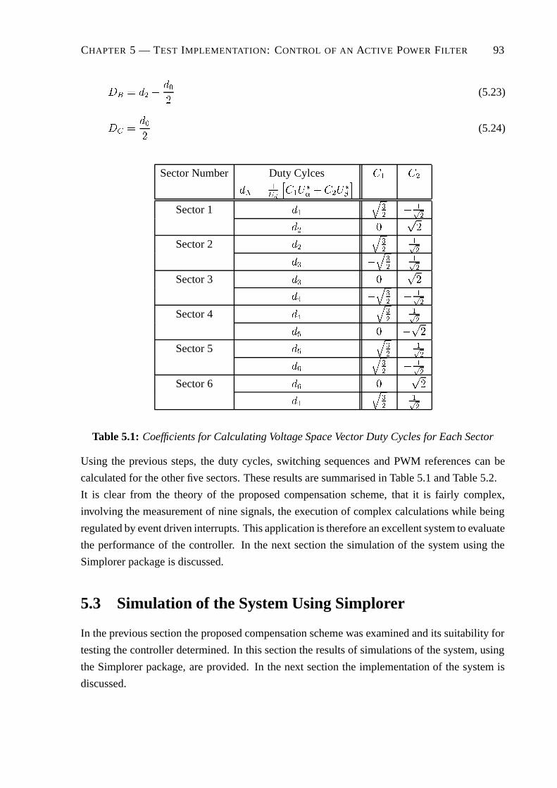
CHAPTER 5 — TEST IMPLEMENTATION: CONTROL OF AN ACTIVE POWER FILTER 93
�� � �� ����
(5.23)
�� ����
(5.24)
Sector Number Duty Cylces �� ��
�$ � �
%�
���,
�� � ��,
��
Sector 1 ��
��
�� ��
�
�� ���
Sector 2 ���
�
�
���
�� ��
�
�
���
Sector 3 �� ���
�� ��
�
�� ��
�
Sector 4 �� ��
�
�
���
� � ���
Sector 5 � ��
�
�� ��
�
���
�
�� ��
�
Sector 6 �� � ���
���
�
�
���
Table 5.1: Coefficients for Calculating Voltage Space Vector Duty Cycles for Each Sector
Using the previous steps, the duty cycles, switching sequences and PWM references can be
calculated for the other five sectors. These results are summarised in Table 5.1 and Table 5.2.
It is clear from the theory of the proposed compensation scheme, that it is fairly complex,
involving the measurement of nine signals, the execution of complex calculations while being
regulated by event driven interrupts. This application is therefore an excellent system to evaluate
the performance of the controller. In the next section the simulation of the system using the
Simplorer package is discussed.
5.3 Simulation of the System Using Simplorer
In the previous section the proposed compensation scheme was examined and its suitability for
testing the controller determined. In this section the results of simulations of the system, using
the Simplorer package, are provided. In the next section the implementation of the system is
discussed.

CHAPTER 5 — TEST IMPLEMENTATION: CONTROL OF AN ACTIVE POWER FILTER 94
Sector Number Switching Sequence PWM Reference
Sector 1 ..01277210.. �� � ���� �� � ��
�� � ���� ��
�� � ���
Sector 2 ..03277230.. �� � ���� ��
�� � ���� �� � ��
�� � ���
Sector 3 ..03477430.. �� � ���
�� � ���� �� � ��
�� � ���� ��
Sector 4 ..05477450.. �� � ���
�� � ���� ��
�� � ���� �� � �
Sector 5 ..05677650.. �� � ���� ��
�� � ���
�� � ���� � � ��
Sector 6 ..01677610.. �� � ���� �� � ��
�� � ���
�� � ���� ��
Table 5.2: PWM Switching Sequences and References for Each Sector

CHAPTER 5 — TEST IMPLEMENTATION: CONTROL OF AN ACTIVE POWER FILTER 95
5.3.1 The Simulation Model
The simulation model consists of three parts: the circuit model and two state machine models.
The one state machine implements the control scheme as shown in the flow diagram in Figure
5.4, while the other controls the switching of the inverter switches. The circuit model is the
schematic representation of the actual hardware components used in the system. Figure 5.13
is a schematic representation of the system hardware used in the simulation. On the top left is
the three-phase source with each phase connected to an ampere meter to measure the source
phase currents. On the top right is a three-phase rectifier connected to a load consisting of the
series combination of an inductor and a resistor. In series with the three phase inputs to the
rectifier are three ampere meters which measures the phase currents supplied to the rectifier.
The bottom half of the diagram is the filter. It consists of three phase-arms (one for each phase
of the system), which each have a filter inductor connected to its output. Current is injected into
the system by varying the average voltage across the filter inductors. To highlight the difference
in the operation of the system with and without the filter operating, switches were inserted in
series with the filter inductors. These switches were set to close after 20ms, connecting the filter
to the plant. Figure 5.14 is a schematic representation of the state machine which implements
L4A+
AM_I_a
A+
AM_I_b
A+
AM_I_c
+ V
VM_E_a+
V
VM_E_b+
V
VM_E_c
t
t
t
A+
AM_Isrc_b
A+
AM_Isrc_c
+ V
VM_out
R1
Three_Phase_Rectifier1
L1 L2 L3
A+
AM_Isrc_a
Three_Phase_Inverter1
E1
E2
Phase_B
Phase_A
Phase_C
L := L_filter L := L_filter L := L_filter
R := R_out
L := L_out
DEL := APF_delay##0.020
Figure 5.13: Simulation Schematic of the System
the control scheme. After the PWM references had been updated in block 7, the state machine
waits in block 1 until the next switching cycle starts. This is the trigger for the state machine
to start calculating the new PWM references. The first step implemented in block 2, consists of
sampling the current and voltage measurements and calculating the voltage reference. Next, in
block 3, the sector of the new voltage reference is calculated. In block 4 the appropriate voltage
space vector duty cycles are calculated for the specific sector. In block 5 the duty cycles are
examined and scaled to ensure that over-modulation does not take place. The duty cycles for the
three phases are calculated in block 6. In block 7 it is used to calculte the new PWM references.
The controller state then returns to block 1 where it again waits for the next switching cycle to
start.
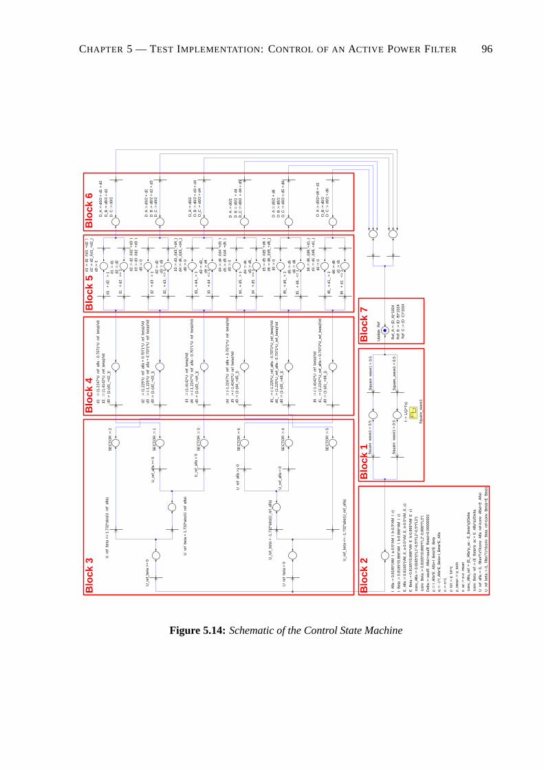
CHAPTER 5 — TEST IMPLEMENTATION: CONTROL OF AN ACTIVE POWER FILTER 96
D_A
:= d
0/2
+ d
1 +
d2
D_B
:= d
0/2
+ d
2D
_C :=
d0/
2
D_B
:= d
0/2
+ d
2 +
d3
D_A
:= d
0/2
+ d
2
D_C
:= d
0/2
D_A
:= d
0/2
D_B
:= d
0/2
+ d
3 +
d4
D_C
:= d
0/2
+ d
4
D_C
:= d
0/2
+ d
4 +
d5
D_A
:= d
0/2
D_B
:= d
0/2
+ d
4
D_A
:= d
0/2
+ d
6
D_C
:=
d0/
2 +
d5
+ d
6D
_B :=
d0/
2
D_A
:= d
0/2+
d6 +
d1
D_C
:= d
0/2
+ d
6D
_B :=
d0
/2
d0 :=
0d2
:= d
2_/(
d1_
+d2
_)d1
:= d
1_/(
d1_+
d2_
)
d1_
+ d
2_ <
= 1
d1_
+ d
2_ >
1
d3
:= d
3_/(
d2_+
d3_)
d2 :=
d2_
/(d2
_+d3
_)
d0 :=
0
d2 :
= d
2_d1
:= d
1_
d2_
+ d
3_ >
1
d2_
+ d
3_ <
= 1d2
:=
d2_
d3 :=
d3_
d4 :=
d4_
/(d
3_+
d4_)
d3
:= d
3_/(
d3_+
d4_)
d0 :
= 0
d4 :=
d4_
d3 :
= d
3_
d3_
+ d
4_ <
= 1
d3_
+ d
4_ >
1
d4_
+ d
5_ >
1
d4 :=
d4_
/(d
4_+
d5_)
d0 :=
0d5
:= d
5_/(
d4_
+d5
_)
d4 :
= d
4_d5
:= d
5_d4
_ +
d5_
<=
1
d5_
+ d
6_ >
1
d6 :=
d6_
/(d5
_+d6
_)d
5 :=
d5_
/(d5
_+d6
_)
d0 :=
0
d5_
+ d
6_ <
= 1d6
:= d
6_d5
:=
d5_
d6_
+ d
1_ >
1
d0 :=
0
d6
:= d
6_/(
d6_+
d1_)
d1 :=
d1_
/(d6
_+d1
_)
d6 :
= d
6_d1
:= d
1_d6
_ +
d1_
<=
1
d1_
:= (
1.2
247*
U_r
ef_a
lfa -
0.7
071*
U_r
ef_b
eta)
/Vd
d2_
:= (
1.41
42*U
_re
f_be
ta)/
Vd
d0 :
= (
1-(d
1_+
d2_
))
d3_
:= (
-1.2
25*U
_ref
_alfa
+ 0
.707
1*U
_ref
_bet
a)/V
dd2
_ :=
(1.
225*
U_r
ef_a
lfa +
0.7
071*
U_
ref_
beta
)/V
d
d0 :
= (
1-(d
2_+
d3_
))
d0 :
= (
1-(d
3_+
d4_
))
d3_
:= (
1.4
142*
U_r
ef_b
eta)
/Vd
d4_
:= (
-1.2
247*
U_r
ef_a
lfa -
0.7
071
*U_r
ef_b
eta)
/Vd
d4_
:= (
-1.2
247*
U_
ref_
alfa
+ 0
.707
1*U
_ref
_bet
a)/V
dd5
_ :=
(-1
.414
2*U
_ref
_bet
a)/V
dd0
:= (
1-(d
4_+
d5_)
)
d6_
:= (
1.22
5*U
_re
f_a
lfa -
0.7
071*
U_r
ef_b
eta)
/Vd
d0 :=
(1-
(d5_
+d
6_))
d5_
:= (
-1.2
25*U
_ref
_alfa
- 0
.707
1*U
_ref
_be
ta)/
Vd
d6_
:= (
-1.4
142*
U_r
ef_b
eta)
/Vd
d0 :=
(1-
(d1_
+d
6_))
d1_
:= (
1.2
247*
U_r
ef_a
lfa +
0.7
071*
U_r
ef_b
eta
)/V
d
U_r
ef_b
eta
>=
0
U_r
ef_b
eta
< 0
U_r
ef_b
eta
>=
1.7
32*a
bs(U
_ref
_alfa
)
U_r
ef_b
eta
< 1
.732
*abs
(U_r
ef_
alfa
)
SE
CT
OR
:=
2
U_r
ef_a
lfa >
= 0
U_r
ef_a
lfa <
0
SE
CT
OR
:=
1
SE
CT
OR
:=
3
U_r
ef_b
eta
> -
1.73
2*a
bs(U
_re
f_al
fa)
U_r
ef_b
eta
<=
-1.
732*
abs(
U_r
ef_a
lfa)
SE
CT
OR
:=
6U
_ref
_alfa
>=
0
U_r
ef_
alfa
< 0
SE
CT
OR
:=
4
SE
CT
OR
:=
5
Upd
ate_
Ref
Squ
are_
wa
ve1
< 0
.5 Squ
are_
wav
e1
Sq
uare
_w
ave1
> 0
.5S
quar
e_w
ave1
< 0
.5
Squ
are_
wav
e1 >
0.5
Ref
_A :=
(D
_A)*
1024
Ref
_B :=
(D
_B)*
1024
Ref
_C :=
(D
_C)*
1024
f :=
1/(
2*T
s)
I_A
lfa :
= 0
.816
5*(A
M_I
_a-0
.5*A
M_I
_b-0
.5*A
M_
I_c)
I_B
eta
:= 0
.816
5*(0
.866
*AM
_I_b
-0.8
66*A
M_I
_c)
E_A
lfa :=
0.8
165
*(V
M_E
_a-0
.5*V
M_E
_b-0
.5*V
M_E
_c)
E_B
eta
:= 0
.816
5*(0
.866
*VM
_E_b
-0.8
66*V
M_E
_c)
p :=
I_A
lfa*E
_Alfa
+I_
Bet
a*E
_Be
ta
q :=
-1*
I_A
lfa*E
_Bet
a+I_
Bet
a*E
_Alfa
Del
ta :=
squ
(E_A
lfa)+
squ(
E_B
eta)
+0.
0000
0001
Icon
v_A
lfa_r
ef :=
(E
_Alfa
*p_a
c -
E_B
eta*
q)/
De
lta
Icon
v_B
eta_
ref :
= (
E_B
eta
*p_a
c +
E_A
lfa*q
)/D
elta
n :=
n+
1
p_t
ot :
= p
_tot
+p
p_m
ean
:= p
_tot
/n
p_a
c :=
p-p
_mea
n
U_r
ef_
alfa
:= (
L_fil
ter/
Ts*
(Ico
nv_A
lfa_r
ef-Ic
onv_
Alfa
)+E
_Alfa
)
U_r
ef_
beta
:= (
L_fil
ter/
Ts*
(Ico
nv_B
eta_
ref-
Icon
v_B
eta
)+E
_Bet
a)
Icon
v_A
lfa :=
0.8
165*
(I"L
1"-0
.5*I
"L2"
-0.5
*I"L
3")
Icon
v_B
eta
:= 0
.816
5*(0
.866
*I"L
2"-0
.866
*I"L
3")
Blo
ck 1
Blo
ck 3
Blo
ck 4
Blo
ck 5
Blo
ck 6
Blo
ck 7
Blo
ck 2
Figure 5.14: Schematic of the Control State Machine
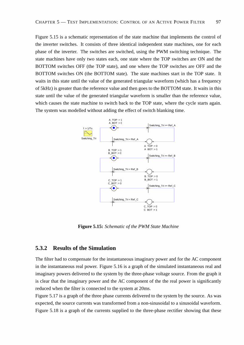
CHAPTER 5 — TEST IMPLEMENTATION: CONTROL OF AN ACTIVE POWER FILTER 97
Figure 5.15 is a schematic representation of the state machine that implements the control of
the inverter switches. It consists of three identical independent state machines, one for each
phase of the inverter. The switches are switched, using the PWM switching technique. The
state machines have only two states each, one state where the TOP switches are ON and the
BOTTOM switches OFF (the TOP state), and one where the TOP switches are OFF and the
BOTTOM switches ON (the BOTTOM state). The state machines start in the TOP state. It
waits in this state until the value of the generated triangular waveform (which has a frequency
of 5kHz) is greater than the reference value and then goes to the BOTTOM state. It waits in this
state until the value of the generated triangular waveform is smaller than the reference value,
which causes the state machine to switch back to the TOP state, where the cycle starts again.
The system was modelled without adding the effect of switch blanking time.
Switching_Tri
Switching_Tri >= Ref_A
Switching_Tri < Ref_A
A_TOP := 1A_BOT := 0
A_TOP := 0A_BOT := 1
Switching_Tri >= Ref_B
Switching_Tri < Ref_B
B_TOP := 1B_BOT := 0
B_TOP := 0B_BOT := 1
Switching_Tri >= Ref_C
Switching_Tri < Ref_C
C_TOP := 1C_BOT := 0
C_TOP := 0C_BOT := 1
f := 1/Ts
Figure 5.15: Schematic of the PWM State Machine
5.3.2 Results of the Simulation
The filter had to compensate for the instantaneous imaginary power and for the AC component
in the instantaneous real power. Figure 5.16 is a graph of the simulated instantaneous real and
imaginary powers delivered to the system by the three-phase voltage source. From the graph it
is clear that the imaginary power and the AC component of the the real power is significantly
reduced when the filter is connected to the system at 20ms.
Figure 5.17 is a graph of the three phase currents delivered to the system by the source. As was
expected, the source currents was transformed from a non-sinusoidal to a sinusoidal waveform.
Figure 5.18 is a graph of the currents supplied to the three-phase rectifier showing that these

CHAPTER 5 — TEST IMPLEMENTATION: CONTROL OF AN ACTIVE POWER FILTER 98
q_srcpsrc
T
220.0
-160.0
0
-100.0
-60.0
40.0
80.0
120.0
160.0
0 40.00m20.00m
Figure 5.16: Instantaneous Real and Imaginary Power Delivered by Source
AM_Isrc_bAM_Isrc_cAM_Isrc_a
T
6.000
-6.000
0
-2.500
2.500
0 40.00m20.00m
Figure 5.17: Three-phase Source Currents
AM_I_aAM_I_bAM_I_c
T
4.000
-4.000
0
-2.500
-1.500
1.000
2.000
3.000
0 40.00m20.00m
Figure 5.18: Three-phase Currents Supplied to the Three-phase Rectifier

CHAPTER 5 — TEST IMPLEMENTATION: CONTROL OF AN ACTIVE POWER FILTER 99
currents are unaffected by the compensator. Figure 5.19 is a graph of the voltage across the load
and Figure 5.20 is a graph of the current supplied to the load. Figure 5.21 is a graph of the
VM_out
T
60.00
0
10.00
20.00
30.00
40.00
50.00
0 40.00m20.00m
Figure 5.19: The Voltage Across the Load
I"L4"
T
3.800
0
0.600
1.000
1.400
1.800
2.200
2.600
3.000
0 40.00m20.00m
Figure 5.20: The Current Supplied to the Load
three-phase currents injected into the system and their calculated references.
Figure 5.22 is a graph of the � and � components of the supply voltage and the reference
voltages of the converter.
From the results obtained from the simulations, it seems that the compensation strategy is valid.
In the next section the system will be implemented in hardware to prove that the PEC33 con-
troller can be used to control a system with this degree of complexity.
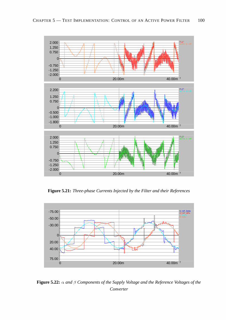
CHAPTER 5 — TEST IMPLEMENTATION: CONTROL OF AN ACTIVE POWER FILTER 100
I"L1"Iconv_a_ref
T
2.000
-2.000
0
-1.250-0.750
0.7501.250
0 40.00m20.00m
I"L2"Iconv_b_ref
T
2.200
-1.800
0
-1.000-0.500
0.7501.250
0 40.00m20.00m
I"L3"Iconv_c_ref
T
2.000
-2.000
0
-1.250-0.750
0.7501.250
0 40.00m20.00m
Figure 5.21: Three-phase Currents Injected by the Filter and their References
U_ref _betaU_ref _alfaE_BetaE_Alfa
T
-75.00
75.00
0
-50.00
-30.00
20.00
40.00
0 40.00m20.00m
Figure 5.22: � and � Components of the Supply Voltage and the Reference Voltages of the
Converter

CHAPTER 5 — TEST IMPLEMENTATION: CONTROL OF AN ACTIVE POWER FILTER 101
5.4 Implementation of the System
In this section the practical implementation of the system is discussed. Section 5.4.1 will ex-
amine the construction of the system and section 5.4.2 the software written to implement the
control algorithm. Results obtained are discussed in section 5.4.3.
5.4.1 The System Hardware
In this section the construction of the system is discussed. Figure 5.23 is a diagram of the whole
system. Most of the building blocks used were not designed specifically for this system, but
+200VDC
Control
Current
Probe
Voltage
Probe
+12VDC+12VDC
3-PhaseRectifier
PEC33 Controller
3-PhaseInverter
0-220VRMS[100VRMS]
Control Signals
CurrentMeasurement
VoltageMeasurement
+5VDC
Figure 5.23: Schematic of the System
were either off-the-shelf components or systems already in use in the laboratory. The off-the-
shelf components included LEM current probes, three-phase and single-phase transformers, a
variac, resistors, inductors and capacitors. The phase-arms used in the system, were developed
in the laboratory for implementing experimental systems like this one. The only circuits specif-
ically designed for this system are the voltage and current probes used to measure the voltages
and currents supplied to the three-phase rectifier. Both the voltage and the current probes have
at their core two operational amplifier circuits. The first is an input buffer and the second sets
the offset and scale of the output signal. The first part of the voltage probe is a voltage di-
vider, which is demonstrated in Figure 5.24. It is used to divide the input voltage of the probe

CHAPTER 5 — TEST IMPLEMENTATION: CONTROL OF AN ACTIVE POWER FILTER 102
Z2
C1
C2
R1 R2Vin Vout
Z1
Figure 5.24: Schematic of the Voltage Divider
(100V&�! or 141V��� maximum) to a voltage between +10V and -10V. To allow for variations
in the input voltage the system was setup for an input voltage of between +160V and -160V.
This implies that the voltage divider should divide the input voltage by a factor of 16. Due to
the parasitic capacitance of resistor ��, the output voltage will be delayed. To compensate for
this effect, an adjustable capacitor, ��, was inserted in parallel with resistor ��. To calculate
the approximate value of capacitor ��, the transfer function of the voltage divider, including the
parasitic and compensation capacitors, is constructed.
����
���
�-�
-� � -�
(5.25)
where -� =&�
��
���
�&��
�
���
is the impedance of �� and ��, and
-� =&�
��
���
�&��
�
���
is the impedance of �� and ��.
It was assumed that -� � -� where k is just a constant. This implies the following:
����
���
��
��
�-�
-� � -�
�
� �
��
��(5.26)
Substituting the equations for -� and -� into eq.5.25 the following equation is obtained:
���
���
�� ��
���
� ��
�
���
�� ��
���
�
��
.� �
&���
� �
��
.� �
&���
���
��
�.� �
&���
.� �
&���
�(5.27)

CHAPTER 5 — TEST IMPLEMENTATION: CONTROL OF AN ACTIVE POWER FILTER 103
From eq.5.27 it follows that if �� is chosen such that �
&���
� �
&���
then:
���
��
���
��
��
��(5.28)
The series combination of two 680k� resistors was chosen for �� providing a total resistance of
1.36M�, which meant that �� had to be 90.67�. A value of ��� was chosen. The parasitic
capacitance of ��, ��, was measured to be approximately 1.5pF, which implies, from eq. 5.28,
that �� should be 22.5pF.
The current probes receive their input from LEM LA 205-S current transducer modules. The
LEM modules have a current measuring range of 0 to��� and the output current is scaled by
a factor of �
����. The simulations indicated that the current supplied to the three-phase rectifier
in each phase is between +10 and -10 ampere. The wires supplying the rectifier was thus wound
ten times around the LEM modules, effectively multiplying the measured current by ten. For
an input current of between +10 and -10A, the output current will then be between +0.05 and
-0.05A. To enable the measurement of an input voltage of between +5V and -5V for this input
current, the current probes have a ���� resistor on their input to GND.
Five different power sources were needed: 100V three-phase, and +5V, +12V, -12V and +200V
DC, as can be seen from the schematic of the system Figure 5.23. The power sources available
in the laboratory were: one fixed 220V three-phase terminal, one variable 220V three-phase
terminal, and various fixed single-phase 220V terminals. Figure 5.25 shows the power supply
configuration for the system. The variable 220V three-phase terminals were used to supply the
100V three-phase voltages. The +200V DC necessary for the inverter was created using the
fixed 220V three-phase terminal. This terminal was connected to the primary side of a three-
phase transformer. The secondary side of the transformer was connected to a three-phase variac.
The output of the variac was connected to a three-phase rectifier. The ripple in the output of the
rectifier was removed by inserting the series combination of two �����F capacitors in parallel
on the output of the rectifier. Parallel to the two capacitors, a resistor bank was inserted to
dissipate the energy stored in the capacitors when the system is shut down. The transformer
was necessary in order to isolate the resultant output from the supply voltage. By adjusting the
variac, a voltage of between 0 and���� ����� � ���V can be obtained. The 200V needed
can thus be achieved. For the +5V, +12V and -12V sources normal (relatively) low power,
power supplies can be used. The neutral of the three-phase terminal is connected to GND in the
substation supplying power to the laboratory. Inductances in the supply lines cause a varying
difference between the output of the neutral connector of the three-phase terminal and GND in
the laboratory. This makes accurate measurement of the three-phase voltages with the probes

CHAPTER 5 — TEST IMPLEMENTATION: CONTROL OF AN ACTIVE POWER FILTER 104
+200VDC
3-PhaseRectifier
220VRMS
0-220VA
C
0-538VDC[200VDC]
220VA
C
3-PhaseVariac
3-PhaseIsolationTrfm
+5VDC 220VRMS0-30VDC [+5VDC]
IsolationTrfm
+12V
DC
+12V
DC
220VRMS
0-30VDC [+12VDC]
IsolationTrfm
0-30VDC [+12VDC]
PowerSupply
PowerSupply
0-220VRMS0-220VRMS[100VRMS] n
n
Figure 5.25: Power Supply Configuration of the System
(which receives its supply voltages relative to GND) impossible. The solution is to connect
the input of the power supplies supplying the power to the PEC33 controller (+5V) and the
probes (+12V and -12V) to isolation transformers and connecting their neutral connections to
the neutral connector of the variable three-phase supply creating a ’virtual’ GND. All of the
voltages in the plant and the controller (that is all the voltages except the inverter voltages) is
then relative to the same reference point.
5.4.2 Implementation of the Control Algorithm in the DSP
The control algorithm was implemented in C and compiled/assembled/linked using the Code
Composer software. The program is listed in section C.5. Figure 5.4, which was explained in
section 5.2.1, is the flowchart for the program. The program starts by configuring the firmware
modules and devices used in the application.
The configuration word which was used for the ADCs (which is defined in table 3.2 in sec-
tion 3.3.3), is 0x0000. In short it configures the ADCs to sample at high speed, using the
external +4.096V voltage reference and disables the channel auto-scan feature. With the auto-
scan feature disabled, each ADC obtains the next sampling channel number from the Chan-
nel Generator module in FPGA Analog as explained in section 4.3.2. The eight channel num-
ber inputs of this module was set as follows: 0 1 2 1 0 1 2 1, because this module outputs the
channel numbers provided by the channel number inputs in sequence from input number 0 to
input number 7. It then starts again at input number 0. The effective sampling sequence is thus:
0 1 2 1 0 1 2 1 0 1 2 1 0 ...
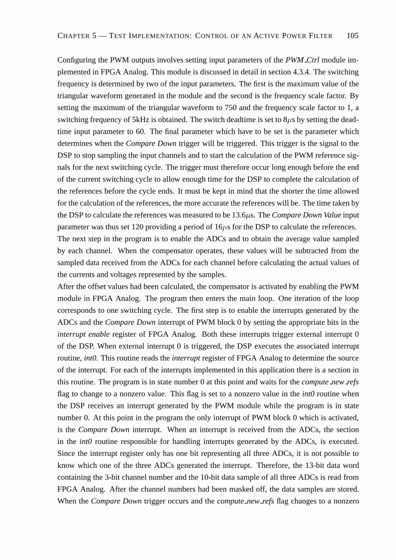
CHAPTER 5 — TEST IMPLEMENTATION: CONTROL OF AN ACTIVE POWER FILTER 105
Configuring the PWM outputs involves setting input parameters of the PWM Ctrl module im-
plemented in FPGA Analog. This module is discussed in detail in section 4.3.4. The switching
frequency is determined by two of the input parameters. The first is the maximum value of the
triangular waveform generated in the module and the second is the frequency scale factor. By
setting the maximum of the triangular waveform to 750 and the frequency scale factor to 1, a
switching frequency of 5kHz is obtained. The switch deadtime is set to 8�s by setting the dead-
time input parameter to 60. The final parameter which have to be set is the parameter which
determines when the Compare Down trigger will be triggered. This trigger is the signal to the
DSP to stop sampling the input channels and to start the calculation of the PWM reference sig-
nals for the next switching cycle. The trigger must therefore occur long enough before the end
of the current switching cycle to allow enough time for the DSP to complete the calculation of
the references before the cycle ends. It must be kept in mind that the shorter the time allowed
for the calculation of the references, the more accurate the references will be. The time taken by
the DSP to calculate the references was measured to be 13.6�s. The Compare Down Value input
parameter was thus set 120 providing a period of 16�s for the DSP to calculate the references.
The next step in the program is to enable the ADCs and to obtain the average value sampled
by each channel. When the compensator operates, these values will be subtracted from the
sampled data received from the ADCs for each channel before calculating the actual values of
the currents and voltages represented by the samples.
After the offset values had been calculated, the compensator is activated by enabling the PWM
module in FPGA Analog. The program then enters the main loop. One iteration of the loop
corresponds to one switching cycle. The first step is to enable the interrupts generated by the
ADCs and the Compare Down interrupt of PWM block 0 by setting the appropriate bits in the
interrupt enable register of FPGA Analog. Both these interrupts trigger external interrupt 0
of the DSP. When external interrupt 0 is triggered, the DSP executes the associated interrupt
routine, int0. This routine reads the interrupt register of FPGA Analog to determine the source
of the interrupt. For each of the interrupts implemented in this application there is a section in
this routine. The program is in state number 0 at this point and waits for the compute new refs
flag to change to a nonzero value. This flag is set to a nonzero value in the int0 routine when
the DSP receives an interrupt generated by the PWM module while the program is in state
number 0. At this point in the program the only interrupt of PWM block 0 which is activated,
is the Compare Down interrupt. When an interrupt is received from the ADCs, the section
in the int0 routine responsible for handling interrupts generated by the ADCs, is executed.
Since the interrupt register only has one bit representing all three ADCs, it is not possible to
know which one of the three ADCs generated the interrupt. Therefore, the 13-bit data word
containing the 3-bit channel number and the 10-bit data sample of all three ADCs is read from
FPGA Analog. After the channel numbers had been masked off, the data samples are stored.
When the Compare Down trigger occurs and the compute new refs flag changes to a nonzero

CHAPTER 5 — TEST IMPLEMENTATION: CONTROL OF AN ACTIVE POWER FILTER 106
value, the program disables all the interrupts generated by FPGA Analog by writing the value
0x0000 to its interrupt enable register. The program is now in state number 1. In this state the
PWM references are calculated. The first step is to convert all nine data samples to the voltages
and currents they represent. Figure 5.26 is a diagram showing the different stages involved in
measuring the supply voltages. The voltages are measured with the voltage probes discussed in
section 5.4.1. The probes convert the input voltages of between +160V and -160V to a voltage
between +4.096V and 0V which is sampled by the ADCs of FPGA Analog. The sampling
process effectively multiplies the input voltage by 250 in order to provide the sampled data
which is an integer between 0 and 1024. Using this diagram a formula for calculating the value
of the supply voltage from the data sample received from the ADC was derived. This formula
is given by eq.5.29.
� � ����� ��
�����
�adc data���
� ������
� ��������adc data� � ��� (5.29)
Figure 5.27 is a diagram showing the different stages involved in measuring the current supplied
to the load. A LEM current transducer module is used to measure the current. It outputs a
current which is a scaled replica of the measured current. These scaled currents generated by
the LEM modules are measured with the current probes, as discussed in section 5.4.1. The
LEM modules and current probes convert the measured current of between +10A and -10A to
a voltage between +4.096V and 0V which is sampled by the ADCs of FPGA Analog. Using
this diagram a formula for calculating the value of the supply current to the load from the data
sample received from the ADC, was derived. This formula is given by eq.5.30.
� ���� �
�����
�adc data���
� ������
� ����������adc data� � �� (5.30)
Figure 5.28 is a diagram showing the different stages involved in measuring the current injected
into the system by the inverter. A LEM current transducer module which is located on the in-
verter, is used to measure the current. The output of the LEM module is converted by additional
circuitry of the inverter to a voltage of between 0V and 5V. These voltages are then sampled by
the ADCs of FPGA Analog. Using this diagram a formula for calculating the value of the the
currents injected into the system by the inverter from the data sample received from the ADC
was derived. This formula is given by eq.5.31.
���# �
���� ������� � ���
� �adc data���
� ����
� ���������adc data�� ������ (5.31)

CHAPTER 5 — TEST IMPLEMENTATION: CONTROL OF AN ACTIVE POWER FILTER 107
[+10V ; -10V]
VoltageScaling & Offset
x 250
ADCFPGA Analog
[+4.096V ; 0V] [1024 ; 0]
PEC33Voltage Probe
VoltageDividerVx:
[+160V ; -160V]
Figure 5.26: Diagram of the Signal Conversions Involved in Measuring the Supply Voltage
LA 205-S
Ix: [+10A ; -10A]
0.0005.(10.Ix):[+0.05A ; -0.05A] [+5V ; -5V]
VoltageScaling & Offset
x 250
ADCFPGA Analog
[+4.096V ; 0V] [1024 ; 0]
PEC33Current Probe
Current-to-Voltage
Converter
Figure 5.27: Diagram of the Signal Conversions Involved in Measuring the Current Supplied
to the Load
LTS 25-NP
Iconvx: [+16A ; -16A]
x 250
ADCFPGA Analog
[1024 ; 0]
PEC33
[+5V ; 0V]
Current-to-Voltage
Converter
Inverter
Figure 5.28: Diagram of the Signal Conversions Involved in Measuring the Current Injected
into the System by the Inverter
CHAPTER 5 — TEST IMPLEMENTATION: CONTROL OF AN ACTIVE POWER FILTER 108
After the measured currents and voltages had been calculated, they are converted to their equiv-
alents in the ��-plane using the Clarke transform given in eq.5.4. The next step is to calculate
the instantaneous real, p, and instantaneous imaginary, q, powers using eq.s 5.7 and 5.8. Next
the alpha and beta components of the reference current, of the current injected into the system
by the inverter, is calculated. In order to do that, the AC component of the instantaneous real
power is needed. This is accomplished by constructing a large circular FIFO array, p arr, which
contains the previous n values of p. Each time the PWM references are to be calculated, the
oldest value of p is removed from the array and subtracted from a variable, which is the sum of
all the p values in the array, namely p tot. The latest value of p is then inserted into the array
into the position of the oldest value and added to p tot. To calculate the current AC compo-
nent of p, p ac, p tot is simply subtracted from p. The reference currents for the inverter are
calculated, using eq.5.12. In order to be able to apply space vector pulse-width modulation,
the reference currents are converted to reference voltages by eq.5.3. Subsequently the sector in
which the voltage reference is located in the ��-plane, is calculated. Using the sector number
and the reference voltage as input, the space vector pulse-width modulation theory is applied
to calculate the duty cycles of the three phase arms. The duty cyles which each have a value
between 0 and 1, is multiplied by the maximum value of the triangular waveform counter in the
PWM block to calculate the references to be applied during the next switching cycle. After the
new references had been calculated, the program enters state number 2. In this state the Counter
Zero trigger is activated. This trigger is triggered when the value of the triangular waveform is
equal to zero. This corresponds to the start of a new switching cycle. The DSP then outputs the
references to FPGA Analog and enables the interrupts of the ADCs. The program then returns
to the beginning of the loop and state number 0.
5.4.3 Results of Implementation
In this section the results obtained using the PEC33 controller to implement the control of a
shunt active power filter, is discussed. The C program implementing the control algorithm is
provided in appendix C.5.
To compare the operation of the system with the results of the simulation obtained in section
5.3.2, the filter was disconnected from the system. The controller, however, was allowed to
operate normally, generating the control signals for the phase-arms of the filter. In all these
tests, the DC bus supplying the inverters was set to 200V and the three-phase AC supply voltage
set to 30V peak.
Figure 5.29 is a graph of the current supplied by phase A of the AC power supply and the
current delivered to phase A of the load (the rectifier). The source current was measured with
a Tektronix current probe (TCP) connected to the oscilloscope. One of the DACs was used to
output the value of the load current, the output of which was measured with a Tektronix voltage
probe (TVP). The two currents should be the same since all the current supplied by the source,

CHAPTER 5 — TEST IMPLEMENTATION: CONTROL OF AN ACTIVE POWER FILTER 109
is delivered to the load. The phase shift is due to the fact that the load current had to be sampled
by the ADCs, and then converted back to an analog representation using the DAC. Comparing
this figure with Figure 5.17, it can be seen that the shape and amplitude of the practical results
compares well with the simulation results.
-5
-4
-3
-2
-1
0
1
2
3
4
5
-0.015 -0.01 -0.005 0 0.005 0.01 0.015 0.02
Time [s]
Cu
rren
t [A
]
Source Current Current Supplied to Load
Figure 5.29: Graph of the Unfiltered Source and Load Currents
Figure 5.30 is a graph of the instantaneous imaginary power and the AC component of the
instantaneous real power delivered to the rectifier. When this graph is compared to Figure
5.16, which represents the simulated values of the instantaneous imaginary power and the AC
component of the instantaneous real power supplied by the source, it can be seen that there
is only a small difference in the amplitudes of the signals displayed in the two graphs. The
only big difference is that the waveform of the simulated instantaneous imaginary power is the
inverse of the waveform measured in the practical system.
Figure 5.31 is a graph of the � and � components of the reference current calculated by the
controller. When this graph is compared to Figure 5.21, which shows the simulated values for
the reference currents, it can be seen that both the shape and amplitudes of the simulated and
practical waveforms are very close.
Figure 5.32 is a graph of the � and � components of the reference voltage calculated by the
controller. When this graph is compared to Figure 5.22, which shows the simulated values for
the reference voltages, it can be seen that both the shape and amplitudes of the simulated and
practical waveforms are very similar.
After the compensator was connected to the system, the results presented in the next six graphs
were obtained. Figure 5.33 is a graph of the currents of phase A of the system. These include

CHAPTER 5 — TEST IMPLEMENTATION: CONTROL OF AN ACTIVE POWER FILTER 110
-200
-150
-100
-50
0
50
100
150
200
-0.01 -0.005 0 0.005 0.01 0.015 0.02 0.025
Time [s]
Po
wer
[W]
AC Component of Instantaneous Real PowerInstantaneous Imaginary Power
Figure 5.30: Graph of the AC Component of the Instantaneous Real Power and Instantaneous
Imaginary Power with the Filter Disabled
-3
-2
-1
0
1
2
3
-0.015 -0.01 -0.005 0 0.005 0.01 0.015 0.02 0.025
Time [s]
Cu
rren
t [A
]
Alpha Component of Converter Reference CurrentBeta Component of Converter Reference Current
Figure 5.31: Graph of the � and � Components of the Reference for the Converter Currents
with the Filter Disabled

CHAPTER 5 — TEST IMPLEMENTATION: CONTROL OF AN ACTIVE POWER FILTER 111
-60
-40
-20
0
20
40
60
-0.01 -0.005 0 0.005 0.01 0.015 0.02 0.025
Time [s]
Vo
ltage
[V
]
V_Alpha V_Alpha Reference
Figure 5.32: Graph of the Alpha Component of the Supply Voltage and its Reference with the
Filter Disabled
the current supplied by the AC source, the current delivered to the rectifier and the current
injected into the system by the compensator in phase A. As required, the current supplied to
the rectifier is unchanged. The current supplied by the AC supply is more sinusoidal than in
the uncompensated case, but is not nearly as good as the simulation results shown in Figure
5.17. This is due to the fact that the amplitude of the currents injected into the system by the
compensator is half the amplitude of the predicted currents by the simulation of the system
given in Figure 5.21.
Figure 5.34 is a graph of the instantaneous imaginary power and the AC component of the
instantaneous real power delivered to the rectifier. As was required, these parameters stayed the
same as for the uncompensated situation.
Figure 5.35 is a graph of the � component of the current injected into the system by the compen-
sator, and its reference. It is clear from the graph that the current does not follow its reference
very well. This is the reason why the current injected into phase A (and the other phases) of the
system as shown in Figure 5.33, is smaller than required.
Figure 5.36 is a graph of the � component of the voltage supplied by the AC supply and the
calculated voltage reference for the compensator. The reference voltage does not seem much
different from the version obtained when the compensator was disconnected from the system.
Figure 5.37 is a graph of the FFT of the currents of phase A of the system. From this graph it
seems that the current supplied by the AC supply has a much better frequency spectrum than
the current supplied to the load, since most of its energy is in its fundamental 50Hz component.

CHAPTER 5 — TEST IMPLEMENTATION: CONTROL OF AN ACTIVE POWER FILTER 112
-5
-4
-3
-2
-1
0
1
2
3
4
5
-0.015 -0.01 -0.005 0 0.005 0.01 0.015 0.02
Time [s]
Cu
rren
t [A
]
AC Source Current Current Supplied to Load
Current Injected by Converter
Figure 5.33: Graph of the Supply Current, Load Current and the Current Injected by the Filter
in Phase A of the System
-150
-100
-50
0
50
100
150
-0.01 -0.005 0 0.005 0.01 0.015 0.02 0.025
Time [s]
Po
wer
[W]
AC Component of Instantaneous Real PowerInstantaneous Imaginary Power
Figure 5.34: Graph of the AC Component of the Instantaneous Real Power and Instantaneous
Imaginary Power Delivered to the Rectifier with the Filter Enabled

CHAPTER 5 — TEST IMPLEMENTATION: CONTROL OF AN ACTIVE POWER FILTER 113
-5
-4
-3
-2
-1
0
1
2
3
4
5
-0.015 -0.01 -0.005 0 0.005 0.01 0.015 0.02 0.025
Time [s]
Cu
rren
t [A
]
Alpha Component of Converter CurrentAlpha Component of Converter Reference Current
Figure 5.35: Graph of the Alpha Component of the Current Injected by the Filter and its
Reference
-100
-80
-60
-40
-20
0
20
40
60
80
100
-0.01 -0.005 0 0.005 0.01 0.015 0.02 0.025
Time [s]
Vo
ltage
[V
]
V_Alpha V_Alpha Reference
Figure 5.36: Graph of the Alpha Component of the Supply Voltage and its Reference with the
Filter Enabled

CHAPTER 5 — TEST IMPLEMENTATION: CONTROL OF AN ACTIVE POWER FILTER 114
-0.05
0
0.05
0.1
0.15
0.2
0.25
0.3
10 100 1000 10000
Time [s]
Cu
rren
t [A
]
Supply Current Load Current Current Injected by Converter
Figure 5.37: Graph of the FFT of the Supply, the Load and the Converter Currents with the
Filter Enabled
Figure 5.38 is a graph of the FFT of the current of the AC supply for the compensated and
uncompensated situation. From this graph it seems that the compensator does not filter the
supply currents at all, but only introduces other frequency components into the load currents.

CHAPTER 5 — TEST IMPLEMENTATION: CONTROL OF AN ACTIVE POWER FILTER 115
-0.05
0
0.05
0.1
0.15
0.2
0.25
0.3
10 100 1000 10000
Time [s]
Cu
rren
t [A
]
Supply Current (Filtered) Supply Current (Unfiltered)
Figure 5.38: Graph of the FFT of the Supply Current with the Filter Enabled and Disabled

Chapter 6
Conclusions
6.1 Summary of the Project
The design, construction and implementation of a power electronic controller was presented
in this thesis. The first step was to define the system specifications. After the specifications
had been defined, components satisfying these specifications, was identified. Then the design
of the system started. The design process can be divided into two phases. The first phase
was the schematic design of the system. During this phase, the logical connections between
the components of the system was made. The second phase involved exporting the netlist of
these connections to the printed circuit board program, where the final layout and physical
connections between the components were made. After the PCB was manufactured and all its
components fitted, some preliminary tests were performed on it. Finally the controller was used
to implement the control of a shunt active power filter.
6.2 Thesis Contribution
The most important contribution of this thesis to power electronic engineering, is the develop-
ment of the reconfigurable power electronic controller, the PEC33. This controller is a versatile
tool which will save power electronic engineers a great deal of time and money. The major ad-
vantage of the controller is its reconfigurability. Not only can the control algorithm implemented
in the DSP of the controller be reconfigured, but also the digital logic design implemented in
the PLDs.
Of secondary importance is the implementation of the control of a shunt active power filter with
the controller. The development of the control system involves the implementation of fairly
complex control theory in the DSP of the controller and the design and construction of voltage
and current probes to enable the ADCs to take measurements of some of the system voltages
and currents. Although, the filter did not work perfectly, the work done in this thesis can be
used as a basis for its further development and perfection.
116
CHAPTER 6 — CONCLUSIONS 117
6.3 Future Work and Recommendations
The most important functions which the PEC33 controller had to provide, was implemented
and tested. These functions include:
� the sampling of measurements with the ADCs
� the analog output of data with the DACs
� providing PWM switch signals
� a user interface consisting of a keypad and LCD
� RS-232 and serial optical communications interface
� non-volatile storage of data
� a reliable clock to keep the system time and date accurate
� a reconfigurable processor with which to implement control algorithms
A function that still have to be tested, is the USB interface. The hardware necessary to imple-
ment the interface was included in the system, but not yet tested.
When the design of the PEC33 was started, the most important components like the DSP, ADCs,
DACs, flash RAM, etc. were above average compared to what was available at that time. Since
then better components had been developed. For example, some of the new DSPs have built-in
high-performance ADCs and some of the new PLDs contain DSP blocks. It would, therefore,
be a worthwhile exercise to do a study on these new devices to determine their usefullness in
future power electronic controller systems.

Bibliography
[1] Constantine H. Houpis, Gary B. Lamont Digital Control Systems - Theory, Hardware,
Software, MacGraw-Hill Book Company, 1985.
[2] John G. Proakis, Dimitris G. Manolakis Digital Signal Processing - Principles,
Algorithms and Applications (Third Edition), Prentice Hall, 1996.
[3] Phil Lapsley, Jeff Bier, Amit Shoham, Edward A. Lee DSP Processor Fundamentals -
Architectures and Features, IEEE Press, 1997.
[4] Howard Johnson, Martin Graham High-Speed Digital Design - A Handbook of Black
Magic, Prentice Hall, 1993.
[5] Ron Mancini, Op Amps for Everyone, Texas Instruments, Literature Number
SLOD006A, September 2001.
[6] TMS320VC33 - Digital Signal Processor, Texas Instruments, Literature Number
SPRS087B, February 1999 (Revised July 2000).
[7] TMS320C3x User’s Guide Texas Instruments, Literature Number SPRU031E, July 1997.
[8] TMS320C3x General-Purpose Applications User’s Guide Texas Instruments, Literature
Number SPRU194, January 1998.
[9] TMS320C3x/C4x Assembly Language Tools User’s Guide Texas Instruments, Literature
Number SPRU035C, February 1998.
[10] JTAG/MPSD Emulation Technical Reference Texas Instruments, Literature Number
SPDU079, December 1994.
[11] XDS51x Emulator Installation Guide Texas Instruments, Literature Number SPNU070,
January 1996.
[12] ACEX 1K - Programmable Logic Family, Altera Corporation, April 2000 (ver 1.01).
[13] MAX 7000B - Programmable Logic Device, Altera Corporation, October 2001 (ver 3.1).
118
BIBLIOGRAPHY 119
[14] Configuring SRAM-Based LUT Devices, Altera Corporation, Application Note 116, April
2000 (ver 1.01).
[15] In-System Programmability in MAX Devices, Altera Corporation, Application Note 95,
June 2000 (ver 1.03).
[16] TLV1570 - 2.7 V to 5.5 V 8-Channel 10-Bit 1.25-MSPS Serial Analog-to-Digital
Converter, Texas Instruments, Literature Number SLAS169B, December 1997 (Revised
October 2000)
[17] AD5302/AD5312/AD5322 - +2.5 V to +5.5 V, 230 �A Dual Rail-to-Rail, Voltage Output
8-/10-/12-Bit DACs, Analog Devices, 1999.
[18] AM29LV200B - 2 Megabit (256 K x 8-Bit/128 K x 16-Bit) CMOS 3.0 Volt-only Boot
Sector Flash Memory, AMD, Publication Number 21521, 13 November 2000.
[19] DS1307 - 64 X 8 Serial Real Time Clock, Dallas Semiconductor.
[20] PDIUSBD12 - USB Interface Device with Parallel Bus, Philips Semiconductors, 8
January 1999.
[21] TLC7701, TLC7725, TLC7703, TLC7733, TLC7705 - Micropower Supply Voltage
Supervisors, Texas Instruments, Literature Number SLVS087K, December 1994
(Revised July 1999).
[22] Hirofumi Akagi, Yoshihira Kanazawa, Akira Nabae, Instantaneous Reactive Power
Compensators Comprising Switching Devices without Energy Storage Components,
IEEE Transactions on Industry Applications, Vol. IA-20, No. 3, May/June 1984.
Appendix A
Schematics
A.1 Schematics of the PEC33
120

CHAPTER A — SCHEMATICS 121
Figure A.1: Schematic of the DSP and Flash RAM of the PEC33 Controller

CHAPTER A — SCHEMATICS 122
97I/O96I/O
90I/O89I/O88I/O87I/O86I/O85I/O
83I/O
93I/O92I/O
95I/O94I/O
111
I/O
99I/O
104
I/O10
3I/O
102
I/O10
1I/O
100
I/O
58I/O57I/O56I/O55I/O
44I/O
45I/O
47I/O
46I/O
60I/O 61I/O63I/O 64I/O 65I/O
68I/O67I/O69I/O 70I/O 71I/O73I/O 74I/O 75I/O
54I/O53I/O
24I/O
28I/O
27I/O
26I/O
25I/O
17I/O
18I/O
15I/O
14I/O
13I/O
12I/O
11I/O
9I/O
8I/O
7I/O
187 I/O
189 I/O
179 I/O177 I/O175 I/O176 I/O
144
I/O
141
I/O14
2I/O
143
I/O
139
I/O14
0I/O
131
I/O13
2I/O
133
I/O13
4I/O
135
I/O13
6I/O
125
I/O12
6I/O
127
I/O12
8I/O
163 I/O160 I/O150 I/O
147 I/O148 I/O149 I/O
174 I/O173 I/O172 I/O170 I/O
167 I/O168 I/O169 I/O
120
I/O12
1I/O
122
I/O30
I/O31
I/O
29I/O
40I/O
41I/O
37I/O
38I/O
39I/O
36I/O
112
I/O11
3I/O
119
I/O
114
I/O11
5I/O
116
I/O
205 I/O203 I/O202 I/O
200 I/O
198 I/O199 I/O
196 I/O197 I/O
195 I/O
193 I/O192 I/O190 I/O191 I/O
166
DA
TA7
164
DA
TA6
162
DA
TA5
6GNDINT 20GNDINT 23GNDINT 32GNDINT 35GNDINT 43GNDINT 49GNDINT 59GNDINT 76GNDINT 82GNDINT 109GNDINT 117GNDINT 123GNDINT 129GNDINT 137GNDINT 145GNDINT 151GNDINT 171GNDINT188GNDINT181GNDINT
80IN
78IN
50TM
S4
TDO
184
IN
183
CLK
182
IN
161
DA
TA4
159
DA
TA3
158
DA
TA2
157
DA
TA1
156
DA
TA0
153
TDI
1TC
K
77V
CC
_CLK
81G
ND
_CLK
84 VCCIO98 VCCIO
194 VCCIO165 VCCIO
110 VCCIO118 VCCIO138 VCCIO146 VCCIO
178 VCCIO
66 VCCIO42 VCCIO34 VCCIO22 VCCIO5 VCCIO
91 VCCINT106 VCCINT
130 VCCINT
185 VCCINT
124 VCCINT
152 VCCINT
201 VCCINT
21 VCCINT
48 VCCINT33 VCCINT
72 VCCINT
62LO
CK
79C
LK/G
CLK
51TR
ST
207
CS
2C
ON
F_D
ON
E
19IN
IT_D
ON
E
186
DEV
_OE
180
DEV
_CLR
n
16R
DY
nBU
SY
155
DC
LK
10C
LKU
SR
108
MSE
L010
7M
SEL1
206
WS
208
CS
204
RS
105
CO
NFI
G52
STA
TUS
154
CE
3C
EO
Figure A.2: Schematic of FPGA Main of the PEC33 Controller

CHAPTER A — SCHEMATICS 123
97I/O96I/O
90I/O89I/O88I/O87I/O86I/O85I/O
83I/O
93I/O92I/O
95I/O94I/O
111
I/O
99I/O
104
I/O10
3I/O
102
I/O10
1I/O
100
I/O
58I/O57I/O56I/O55I/O
44I/O
45I/O
47I/O
46I/O
60I/O 61I/O63I/O 64I/O 65I/O
68I/O67I/O69I/O 70I/O 71I/O73I/O 74I/O 75I/O
54I/O53I/O
24I/O
28I/O
27I/O
26I/O
25I/O
17I/O
18I/O
15I/O
14I/O
13I/O
12I/O
11I/O
9I/O
8I/O
7I/O
187 I/O
189 I/O
179 I/O177 I/O175 I/O176 I/O
144
I/O
141
I/O14
2I/O
143
I/O
139
I/O14
0I/O
131
I/O13
2I/O
133
I/O13
4I/O
135
I/O13
6I/O
125
I/O12
6I/O
127
I/O12
8I/O
163 I/O160 I/O150 I/O
147 I/O148 I/O149 I/O
174 I/O173 I/O172 I/O170 I/O
167 I/O168 I/O169 I/O
120
I/O12
1I/O
122
I/O30
I/O31
I/O
29I/O
40I/O
41I/O
37I/O
38I/O
39I/O
36I/O
112
I/O11
3I/O
119
I/O
114
I/O11
5I/O
116
I/O
205 I/O203 I/O202 I/O
200 I/O
198 I/O199 I/O
196 I/O197 I/O
195 I/O
193 I/O192 I/O190 I/O191 I/O
166
DA
TA7
164
DA
TA6
162
DA
TA5
6GNDINT 20GNDINT 23GNDINT 32GNDINT 35GNDINT 43GNDINT 49GNDINT 59GNDINT 76GNDINT 82GNDINT 109GNDINT 117GNDINT 123GNDINT 129GNDINT 137GNDINT 145GNDINT 151GNDINT 171GNDINT188GNDINT181GNDINT
80IN
78IN
50TM
S4
TDO
184
IN
183
CLK
182
IN
161
DA
TA4
159
DA
TA3
158
DA
TA2
157
DA
TA1
156
DA
TA0
153
TDI
1TC
K
77V
CC
_CLK
81G
ND
_CLK
84 VCCIO98 VCCIO
194 VCCIO165 VCCIO
110 VCCIO118 VCCIO138 VCCIO146 VCCIO
178 VCCIO
66 VCCIO42 VCCIO34 VCCIO22 VCCIO5 VCCIO
91 VCCINT106 VCCINT
130 VCCINT
185 VCCINT
124 VCCINT
152 VCCINT
201 VCCINT
21 VCCINT
48 VCCINT33 VCCINT
72 VCCINT
62LO
CK
79C
LK/G
CLK
51TR
ST
207
CS
2C
ON
F_D
ON
E
19IN
IT_D
ON
E
186
DEV
_OE
180
DEV
_CLR
n
16R
DY
nBU
SY
155
DC
LK
10C
LKU
SR
108
MSE
L010
7M
SEL1
206
WS
208
CS
204
RS
105
CO
NFI
G52
STA
TUS
154
CE
3C
EO
Figure A.3: Schematic of FPGA Analog of the PEC33 Controller

CHAPTER A — SCHEMATICS 124
Figure A.4: Schematic of the Ports and Drivers of the PEC33 Controller

CHAPTER A — SCHEMATICS 125
Figure A.5: Schematic of the Analog-to-Digital Converters of the PEC33 Controller

CHAPTER A — SCHEMATICS 126
Figure A.6: Schematic of the Digital-to-Analog Converters of the PEC33 Controller

CHAPTER A — SCHEMATICS 127
86GNDINT38GNDINT
95GNDIO74GNDIO59GNDIO43GNDIO26GNDIO11GNDIO
91 VCCINT39 VCCINT
51 VCCIO266 VCCIO282 VCCIO2
34 VCCIO118 VCCIO13 VCCIO1
87IN
PUT/
GC
LK1
88IN
PUT/
OE1
89IN
PUT/
GC
LRn
90IN
PUT/
OE2
/GC
LK2
73TD
O15
TMS
4TD
I
62TC
K
12V
REF
A60
VR
EFB
17I/O
19I/O
20I/O
21I/O
22I/O
23I/O
24I/O
25I/O
16I/O
27I/O 28I/O 29I/O 30I/O 31I/O 32I/O 33I/O35I/O 36I/O 37I/O
42I/O41I/O40I/O
48I/O47I/O46I/O45I/O44I/O
50I/O49I/O
52I/O
53I/O
54I/O
55I/O
56I/O
57I/O
58I/O
61I/O
1I/O
2I/O
5I/O
6I/O
7I/O
8I/O
9I/O
10I/O
13I/O
14I/O
63I/O
64I/O
65I/O
67I/O
68I/O
69I/O
70I/O
71I/O
72I/O
75I/O
99 I/O100 I/O
96 I/O97 I/O98 I/O
92 I/O93 I/O94 I/O
83 I/O84 I/O85 I/O
76 I/O77 I/O78 I/O79 I/O80 I/O81 I/O
Figure A.7: Schematic of EPLD ExBus and the Expansion ports of the PEC33 Controller

CHAPTER A — SCHEMATICS 128
Figure A.8: Schematic of the Power Supply and Reset Circuitry of the PEC33 Controller

CHAPTER A — SCHEMATICS 129
A.2 Schematics of the PEC33 Optical Fibre Expansion
Board
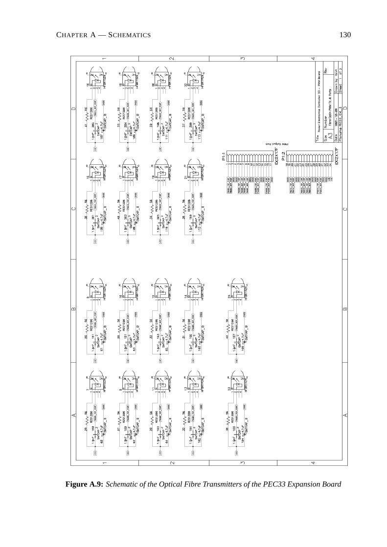
CHAPTER A — SCHEMATICS 130
Figure A.9: Schematic of the Optical Fibre Transmitters of the PEC33 Expansion Board

CHAPTER A — SCHEMATICS 131
Figure A.10: Schematic of the Optical Fibre Receivers of the PEC33 Expansion Board
CHAPTER A — SCHEMATICS 132
A.3 Schematics of the Voltage and Current Probes
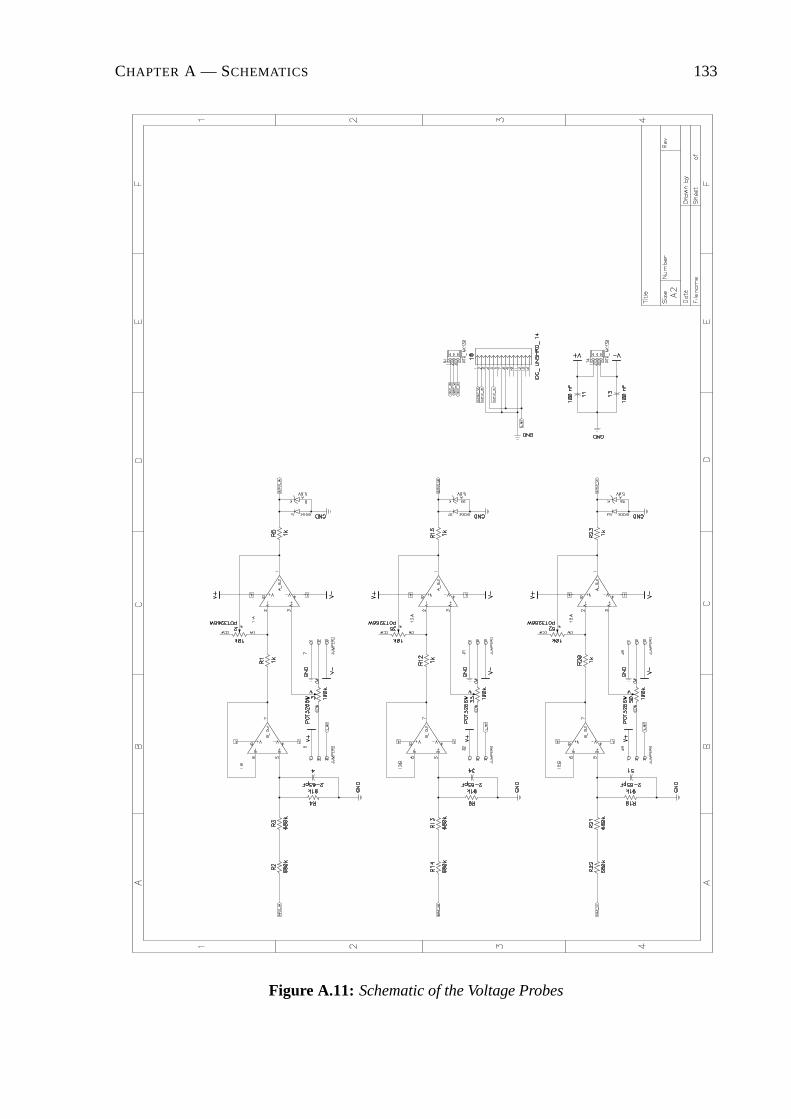
CHAPTER A — SCHEMATICS 133
Figure A.11: Schematic of the Voltage Probes
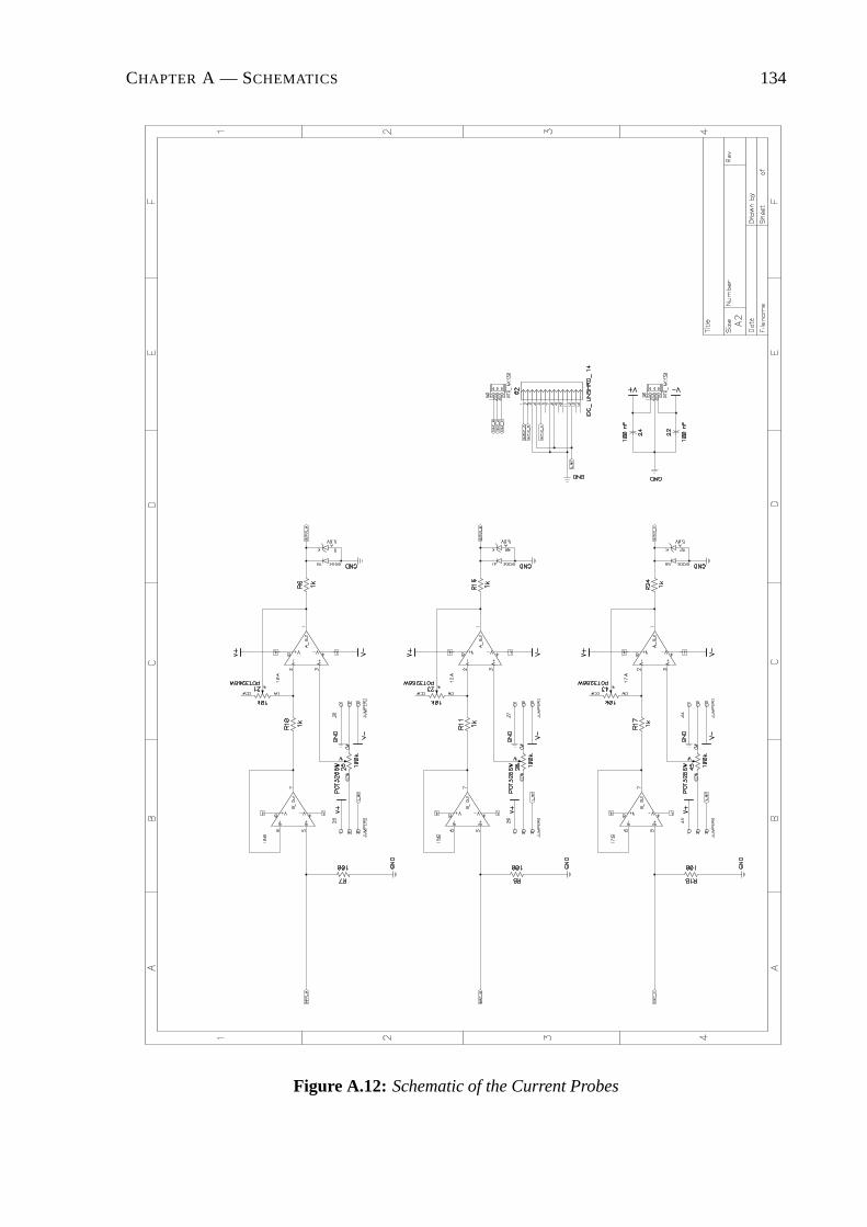
CHAPTER A — SCHEMATICS 134
Figure A.12: Schematic of the Current Probes

Appendix B
Printed Circuit Board Layouts
B.1 Printed Circuit Board Layout of the PEC33
135

CHAPTER B — PRINTED CIRCUIT BOARD LAYOUTS 136
Figure B.1: Printed Circuit Board Layout of the PEC33 TOP and BOTTOM Silk Layers
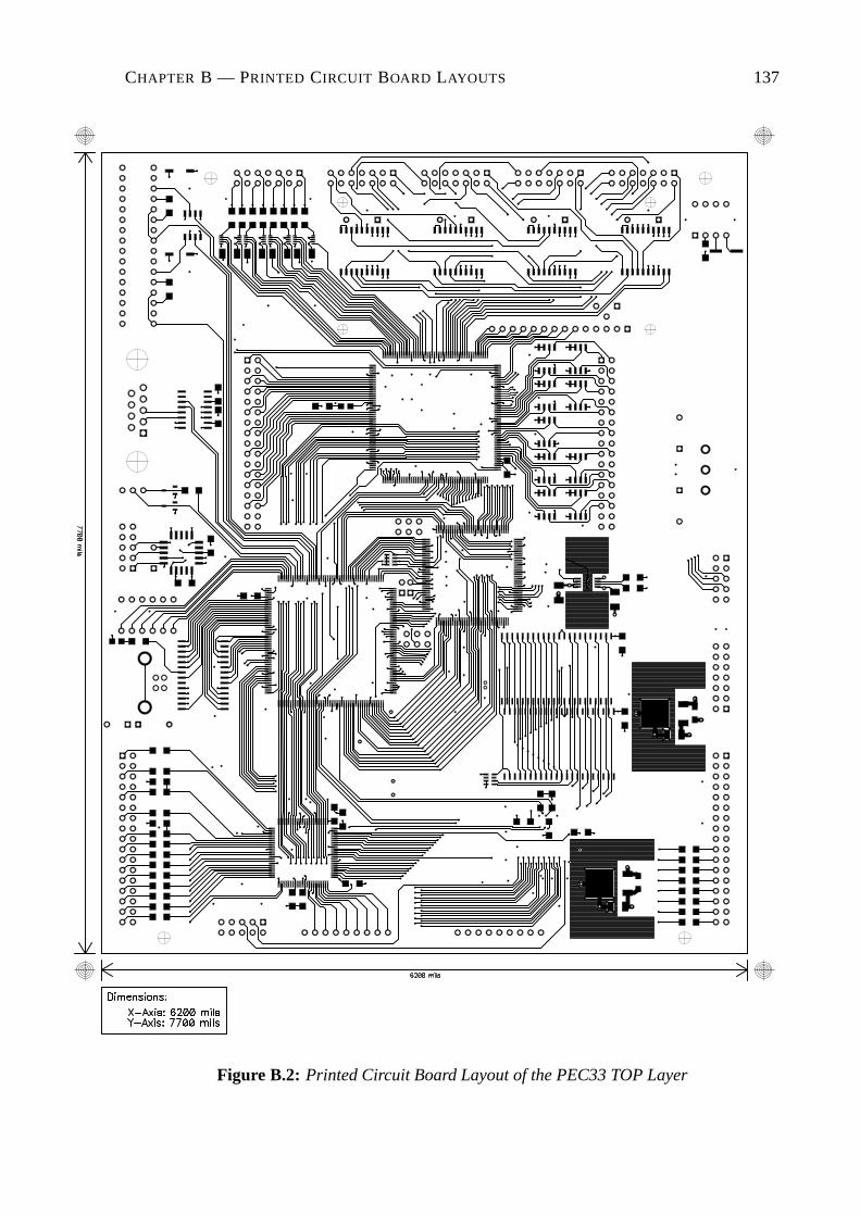
CHAPTER B — PRINTED CIRCUIT BOARD LAYOUTS 137
Figure B.2: Printed Circuit Board Layout of the PEC33 TOP Layer

CHAPTER B — PRINTED CIRCUIT BOARD LAYOUTS 138
Figure B.3: Printed Circuit Board Layout of the PEC33 BOTTOM Layer
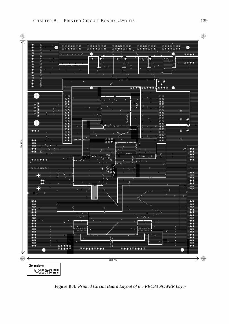
CHAPTER B — PRINTED CIRCUIT BOARD LAYOUTS 139
Figure B.4: Printed Circuit Board Layout of the PEC33 POWER Layer

CHAPTER B — PRINTED CIRCUIT BOARD LAYOUTS 140
Figure B.5: Printed Circuit Board Layout of the PEC33 Ground Layer

CHAPTER B — PRINTED CIRCUIT BOARD LAYOUTS 141
B.2 Printed Circuit Board Layout of the PEC33 Optical
Fibre Expansion Board

CHAPTER B — PRINTED CIRCUIT BOARD LAYOUTS 142
Figure B.6: Printed Circuit Board Layout of the Expansion Board TOP Layer

CHAPTER B — PRINTED CIRCUIT BOARD LAYOUTS 143
Figure B.7: Printed Circuit Board Layout of the Expansion Board BOT Layer

CHAPTER B — PRINTED CIRCUIT BOARD LAYOUTS 144
B.3 Printed Circuit Board Layout of the Voltage and
Current Probes
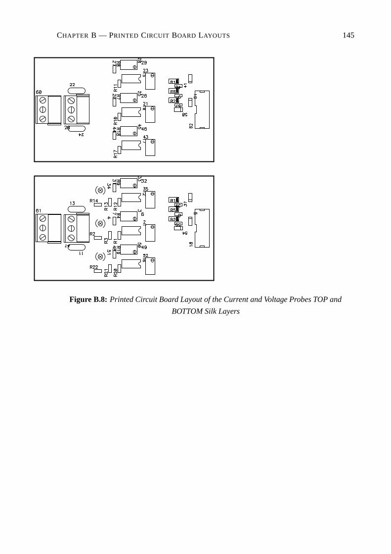
CHAPTER B — PRINTED CIRCUIT BOARD LAYOUTS 145
Figure B.8: Printed Circuit Board Layout of the Current and Voltage Probes TOP and
BOTTOM Silk Layers
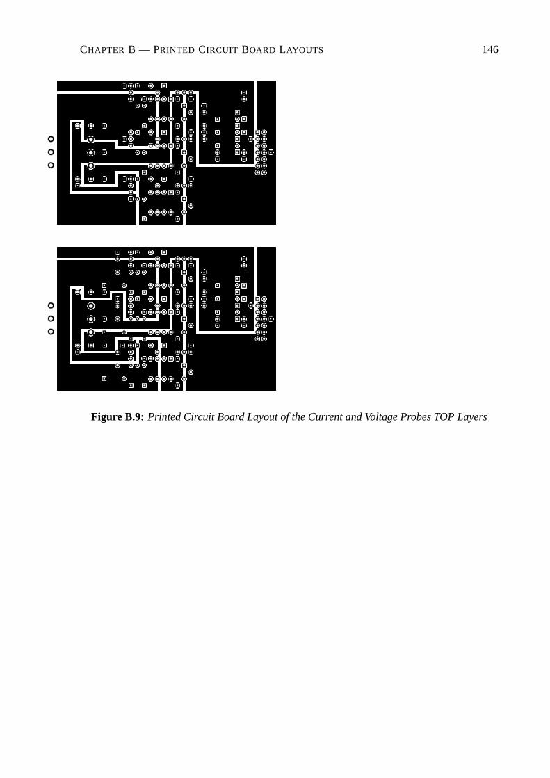
CHAPTER B — PRINTED CIRCUIT BOARD LAYOUTS 146
Figure B.9: Printed Circuit Board Layout of the Current and Voltage Probes TOP Layers

CHAPTER B — PRINTED CIRCUIT BOARD LAYOUTS 147
Figure B.10: Printed Circuit Board Layout of the Current and Voltage Probes BOTTOM
Layers

Appendix C
DSP C Example Programs
148

CHAPTER C — DSP C EXAMPLE PROGRAMS 149
C.1 The Header File Containing the Address Definitions,
PEC33 Address.h
/* Header file containing register address declarations and constant definitions */
/* DSP Main constant definitions */
/* Serie port */
#define global_ctrl 0
#define tx_ctrl 2
#define rx_ctrl 3
#define timer_ctrl 4
#define timer_cntr 5
#define timer_period 6
#define tx_data 8
#define rx_data 0xC
/* DSP register address declarations */
volatile int *serie0 = (int *) 0x808040;
/* FPGA Main constant definitions */
#define rtc_status 0
#define rtc_wr_addr 1
/* FPGA Main register address declarations */
volatile int *RS232Port=(int *) 0x500000;
volatile int *fram_reg=(int *) 0x500008;
volatile int *rtc=(int *) 0x500010;
volatile int *rtc_wr_data=(int *) 0x500012;
volatile int *rtc_rd_data=(int *) 0x500013;
volatile int *main_cmd0=(int *) 0x500066;
volatile int *main_cmd1=(int *) 0x500067;
/* FRAM constant definitions */
#define TX_Data 0
#define RX_Data 1
#define Status 2
#define BaudRate 3
#define fram_status 0
/* FRAM register address declarations */
volatile int *fram0=(int *) 0x400000;
volatile int *fram1=(int *) 0xC00000;
/* FPGA Analog constant definitions */
/* DAC registers */
#define ctrl_addr 0
CHAPTER C — DSP C EXAMPLE PROGRAMS 150
#define a_conf_addr 1
#define a_data_addr 2
#define b_conf_addr 3
#define b_data_addr 4
/* ADC Registers */
#define adc_conf_addr 0
#define adc_data_addr 1
#define adc_samp_chan0_addr 2
#define adc_samp_chan1_addr 3
#define adc_samp_chan2_addr 4
#define adc_samp_chan3_addr 5
#define adc_samp_chan4_addr 6
#define adc_samp_chan5_addr 7
#define adc_samp_chan6_addr 8
#define adc_samp_chan7_addr 9
/* LCD Registers */
#define mode_addr 0
#define char_addr 1
#define addr_addr 2
#define status_addr 3
/* PWM Registers */
#define pwm_refa_addr 0
#define pwm_refb_addr 1
#define pwm_refc_addr 2
#define pwm_refn_addr 3
#define pwm_trimax_addr 4
#define pwm_trifreqscale_addr 5
#define pwm_deadtime_addr 6
#define pwm_upval_addr 7
#define pwm_downval_addr 8
#define dac0_load_cmd 1 /* 00000001b */
#define dac1_load_cmd 2 /* 00000010b */
#define dac2_load_cmd 4 /* 00000100b */
#define dac3_load_cmd 8 /* 00001000b */
#define lcd_updatemode_cmd 16 /* 00010000b */
#define lcd_updatedata_cmd 32 /* 00100000b */
#define lcd_reset_cmd 64 /* 01000000b */
#define adc0_en_cmd 1 /* 00000001b */
#define adc1_en_cmd 2 /* 00000010b */
#define adc2_en_cmd 4 /* 00000100b */
#define adc3_en_cmd 8 /* 00001000b */
#define pwm0_en_cmd 16 /* 00010000b */
#define pwm1_en_cmd 32 /* 00100000b */
/* FPGA Analog register address declarations */
volatile int *dac0=(int *) 0x600000;
volatile int *dac1=(int *) 0x600008;
volatile int *dac2=(int *) 0x600010;
volatile int *dac3=(int *) 0x600018;
volatile int *adc_status=(int *) 0x600020;
/*Register to show which adc have new data ready --- 4 Bits

CHAPTER C — DSP C EXAMPLE PROGRAMS 151
||---------||---------||---------||---------||
|| 3 || 2 || 1 || 0 ||
|| ADC3 || ADC2 || ADC1 || ADC0 ||
|| Ready || Ready || Ready || Ready ||
||---------||---------||---------||---------|| */
volatile int *adc0=(int *) 0x600021;
volatile int *adc1=(int *) 0x60002B;
volatile int *adc2=(int *) 0x600035;
volatile int *adc3=(int *) 0x60003F;
volatile int *lcd=(int *) 0x600049;
volatile int *pwm_status=(int *) 0x60004D;
volatile int *pwm0=(int *) 0x60004E;
volatile int *pwm1=(int *) 0x600057;
volatile int *pwm_err_top=(int *) 0x600060;
volatile int *pwm_err_bot=(int *) 0x600061;
volatile int *fpganlg_int_en=(int *) 0x600062;
/*Register to enable the different interrupt sources --- 15 Bits
||---------||---------||---------||---------||---------||---------||---------||---------||
|| 14 || 13 || 12 || 11 || 10 || 9 || 8 || 7 ||
|| PWM1 || PWM1 || PWM1 || PWM1 || PWM0 || PWM0 || PWM0 || PWM0 ||
|| Counter || Ramp || Compare || Compare || Counter || Ramp || Compare || Compare ||
|| Zero || Dir || Down || Up || Zero || Dir || Down || Up ||
||---------||---------||---------||---------||---------||---------||---------||---------||
|| 6 || 5 || 4 || 3 || 2 || 1 || 0 ||
|| PWM || PWM || Keypad || adc3 || adc2 || adc1 || adc0 ||
|| Error || Error || || || || || ||
|| Bot || Top || || || || || ||
||---------||---------||---------||---------||---------||---------||---------||*/
volatile int *keyval=(int *) 0x600063;
volatile int *fpganlg_int_reg=(int *) 0x600065;
/*Register show which entity caused interrupt --- 6 Bits
||---------||---------||---------||---------||---------||---------||
|| 5 || 4 || 3 || 2 || 1 || 0 ||
|| PWM1 || PWM0 || PWM || PWM || Keypad || adc ||
|| status || status || Error || Error || || ||
|| || || Bot || Top || || ||
||---------||---------||---------||---------||---------||---------|| */
volatile int *analog_cmd0=(int *) 0x600066;
volatile int *analog_cmd1=(int *) 0x600067;
unsigned int *int2_addr=(unsigned int *) 0x809FC3;

CHAPTER C — DSP C EXAMPLE PROGRAMS 152
C.2 The DSP C Program to Copy Serial Input Data to
FRAM 0, SERIAL2FRAM.c/* This program copies data received with the DSP’s serial
port to sector 0 of FRAM 0, the address where the DSP
loads its program from when it boots from FRAM 0.
*/
#include <string.h>
#include <math.h>
#include <stdlib.h>
#include <float.h>
#include <limits.h>
#include "Address2.h"
#define pi (double)3.14159265359
#define mask10 1023
asm(" .sect \"vectors\" ");
asm(" NOP ");
asm(" NOP ");
asm(" NOP ");
asm(" NOP ");
asm(" NOP ");
asm(" BU _intR ");
unsigned int addr;
unsigned int data;
unsigned int rx_arr[4096];
unsigned int arr_cntr;
unsigned int downloadStarted;
unsigned int downloadCounter;
void analog_doCmd0( int cmd )
{
*analog_cmd0 = cmd;
*analog_cmd0 = 0;
}
void analog_doCmd1( int cmd )
{
*analog_cmd1 = cmd;
}
void myDelay( int cntr )
{
int i_cntr;
i_cntr = 0;
while ( i_cntr < cntr ) {
i_cntr++;
}
CHAPTER C — DSP C EXAMPLE PROGRAMS 153
}
/* Procedure that erases the data of sector, sect_addr, of FRAM 0 */
void eraseSector ( unsigned int sect_addr )
{
int addr;
int status;
if ( sect_addr > 6 ) exit;
/* Determine the sector address */
switch ( sect_addr )
{
case 0:
addr = 0;
break;
case 1:
addr = 2*0x08000;
break;
case 2:
addr = 2*0x10000;
break;
case 3:
addr = 2*0x18000;
break;
case 4:
addr = 2*0x1C000;
break;
case 5:
addr = 2*0x1D000;
break;
case 6:
addr = 2*0x1E000;
break;
default:
break;
}
/* Wait until FRAM 0 is ready */
status = fram_reg[fram_status]&1;
while ( status == 0 ) {
myDelay(100);
status = fram_reg[fram_status]&1;
}
/* Output erase command sequence */
fram0[0xAAA] = (unsigned int)(0xAA);
fram0[0x555] = (unsigned int)(0x55);
fram0[0xAAA] = (unsigned int)(0x80);
fram0[0xAAA] = (unsigned int)(0xAA);
fram0[0x555] = (unsigned int)(0x55);
fram0[addr] = (unsigned int)(0x30);
myDelay( 7000 );
}
/* Procedure that writes a byte, data, to address, addr, in FRAM 0 */
void writeByte ( unsigned int addr, unsigned int data )
{
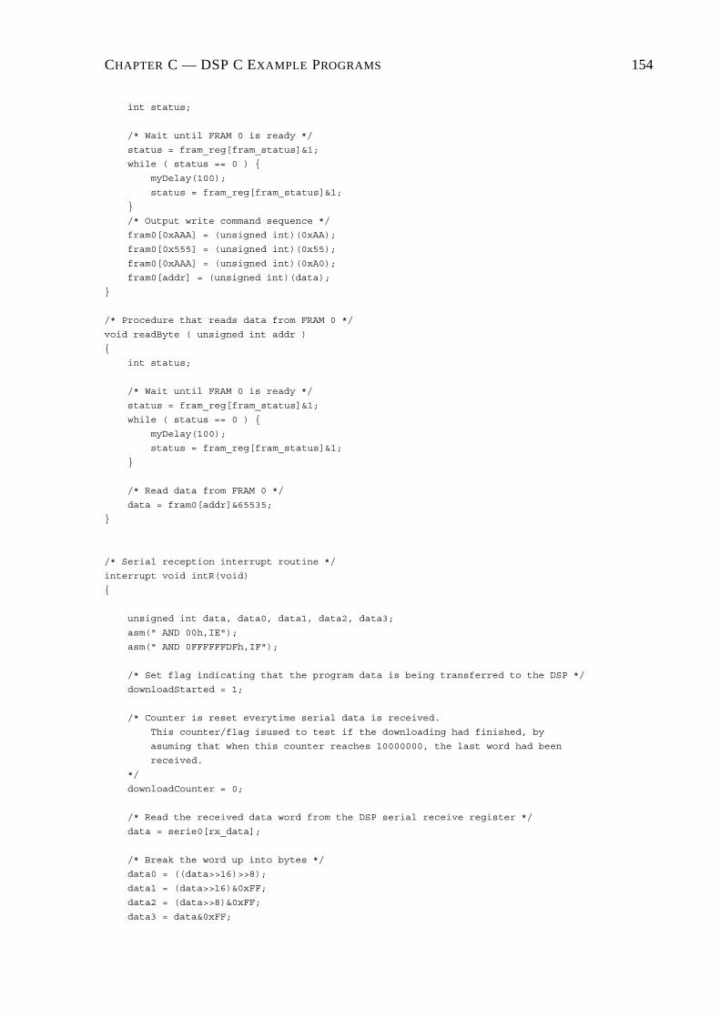
CHAPTER C — DSP C EXAMPLE PROGRAMS 154
int status;
/* Wait until FRAM 0 is ready */
status = fram_reg[fram_status]&1;
while ( status == 0 ) {
myDelay(100);
status = fram_reg[fram_status]&1;
}
/* Output write command sequence */
fram0[0xAAA] = (unsigned int)(0xAA);
fram0[0x555] = (unsigned int)(0x55);
fram0[0xAAA] = (unsigned int)(0xA0);
fram0[addr] = (unsigned int)(data);
}
/* Procedure that reads data from FRAM 0 */
void readByte ( unsigned int addr )
{
int status;
/* Wait until FRAM 0 is ready */
status = fram_reg[fram_status]&1;
while ( status == 0 ) {
myDelay(100);
status = fram_reg[fram_status]&1;
}
/* Read data from FRAM 0 */
data = fram0[addr]&65535;
}
/* Serial reception interrupt routine */
interrupt void intR(void)
{
unsigned int data, data0, data1, data2, data3;
asm(" AND 00h,IE");
asm(" AND 0FFFFFFDFh,IF");
/* Set flag indicating that the program data is being transferred to the DSP */
downloadStarted = 1;
/* Counter is reset everytime serial data is received.
This counter/flag isused to test if the downloading had finished, by
asuming that when this counter reaches 10000000, the last word had been
received.
*/
downloadCounter = 0;
/* Read the received data word from the DSP serial receive register */
data = serie0[rx_data];
/* Break the word up into bytes */
data0 = ((data>>16)>>8);
data1 = (data>>16)&0xFF;
data2 = (data>>8)&0xFF;
data3 = data&0xFF;

CHAPTER C — DSP C EXAMPLE PROGRAMS 155
/* Store the received bytes in the receive array, rx_arr */
if ( arr_cntr < 4096 ) {
rx_arr[arr_cntr] = data3;
rx_arr[arr_cntr+1] = data2;
rx_arr[arr_cntr+2] = data1;
rx_arr[arr_cntr+3] = data0;
arr_cntr = arr_cntr+4;
}
asm(" OR 20h,IE");
asm(" OR 2000h,ST");
}
main(void)
{
unsigned int i,j;
unsigned int dummy;
unsigned int out_data;
unsigned int status;
unsigned int *prim_bus_ctrl = (unsigned int *)0x808064;
*prim_bus_ctrl = 0x10C8;
asm(" OR 00h,IE"); /*asm(" OR 20h,IE"); */
asm(" OR 0000h,ST");
downloadStarted = 0;
downloadCounter = 0;
arr_cntr = 0;
i = 0;
while (i<4096) {
rx_arr[i] = 0x00000000;
i++;
}
serie0[global_ctrl] = 0x0EB00044;
serie0[tx_ctrl] = 0x00000333;
serie0[rx_ctrl] = 0x00000111;
serie0[timer_ctrl] = 0x000001CF;
serie0[timer_cntr] = 0x00;
serie0[timer_period] = 0x00010001;
RS232Port[BaudRate] = 3;
asm(" OR 20h,IE");
asm(" OR 2000h,ST");
/* Wait for download to start */
downloadStarted = 0;
while (downloadStarted == 0)
{
}
/* Wait for download to finish -- counter is reset each time data is received */
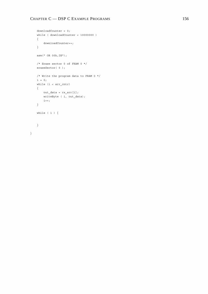
CHAPTER C — DSP C EXAMPLE PROGRAMS 156
downloadCounter = 0;
while ( downloadCounter < 10000000 )
{
downloadCounter++;
}
asm(" OR 00h,IE");
/* Erase sector 0 of FRAM 0 */
eraseSector( 0 );
/* Write the program data to FRAM 0 */
i = 0;
while (i < arr_cntr)
{
out_data = rx_arr[i];
writeByte ( i, out_data);
i++;
}
while ( 1 ) {
}
}

CHAPTER C — DSP C EXAMPLE PROGRAMS 157
C.3 The DSP C Program to Test the Liquid Crystal Display,
LCD Test1.c/* LCD test program
It seems that the first character written to the
LCD is lost, therefore first write a dummy character.
*/
#include <string.h>
#include <math.h>
#include <stdlib.h>
#include <float.h>
#include <limits.h>
#include "PEC33_Address.h"
#define pi (double)3.14159265359
#define mask10 1023
asm(" .sect \"vectors\" ");
asm(" NOP ");
asm(" NOP ");
asm(" NOP ");
int pos;
void analog_doCmd0( int cmd )
{
*analog_cmd0 = cmd;
*analog_cmd0 = 0;
}
void analog_doCmd1( int cmd )
{
*analog_cmd1 = cmd;
}
void Mode( int mode, int delay )
{
int status;
status = 0;
/* Copy LCD mode data to FPGA Analog */
lcd[mode_addr] = mode;
/* Check if LCD is ready -- status = 1 */
status = lcd[status_addr]&1;
while ( status == 0 ) {
status = lcd[status_addr]&1;
}
/* Update the LCD mode */

CHAPTER C — DSP C EXAMPLE PROGRAMS 158
analog_doCmd0(lcd_updatemode_cmd);
/* Execute delay */
status = 0;
while ( status < delay ) {
status++;
}
}
void DisplayChar( int lcdaddr, char lcddata, int delay )
{
int status;
status = 0;
/* Copy LCD character data to FPGA Analog */
lcd[char_addr] = lcddata;
/* Copy LCD address data to FPGA Analog */
lcd[addr_addr] = lcdaddr;
/* Check if LCD is ready -- status = 1 */
status = lcd[status_addr]&1;
while ( status == 0 ) {
status = lcd[status_addr]&1;
}
/* Update the LCD */
analog_doCmd0(lcd_updatedata_cmd);
/* Execute delay */
status = 0;
while ( status < delay ) {
status++;
}
}
main(void)
{
int i;
unsigned int *prim_bus_ctrl = (unsigned int *)0x808064;
*prim_bus_ctrl = 0x10F8;
/* Disable interrupts */
asm(" OR 0h,IE");
asm(" OR 2000h,ST");
i = 0;
while (i<13000000) {
i++;
}
/* Initialize the LCD */
Mode( 0x30, 300000 );
Mode( 0x30, 10000 );
Mode( 0x30, 0 );
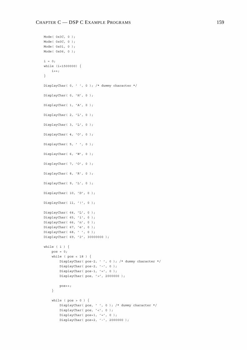
CHAPTER C — DSP C EXAMPLE PROGRAMS 159
Mode( 0x3C, 0 );
Mode( 0x0C, 0 );
Mode( 0x01, 0 );
Mode( 0x06, 0 );
i = 0;
while (i<1500000) {
i++;
}
DisplayChar( 0, ’ ’, 0 ); /* dummy character */
DisplayChar( 0, ’H’, 0 );
DisplayChar( 1, ’A’, 0 );
DisplayChar( 2, ’L’, 0 );
DisplayChar( 3, ’L’, 0 );
DisplayChar( 4, ’O’, 0 );
DisplayChar( 5, ’ ’, 0 );
DisplayChar( 6, ’W’, 0 );
DisplayChar( 7, ’O’, 0 );
DisplayChar( 8, ’R’, 0 );
DisplayChar( 9, ’L’, 0 );
DisplayChar( 10, ’D’, 0 );
DisplayChar( 11, ’!’, 0 );
DisplayChar( 64, ’L’, 0 );
DisplayChar( 65, ’i’, 0 );
DisplayChar( 66, ’n’, 0 );
DisplayChar( 67, ’e’, 0 );
DisplayChar( 68, ’ ’, 0 );
DisplayChar( 69, ’2’, 30000000 );
while ( 1 ) {
pos = 0;
while ( pos < 18 ) {
DisplayChar( pos-2, ’ ’, 0 ); /* dummy character */
DisplayChar( pos-2, ’-’, 0 );
DisplayChar( pos-1, ’=’, 0 );
DisplayChar( pos, ’>’, 2000000 );
pos++;
}
while ( pos > 0 ) {
DisplayChar( pos, ’ ’, 0 ); /* dummy character */
DisplayChar( pos, ’<’, 0 );
DisplayChar( pos+1, ’=’, 0 );
DisplayChar( pos+2, ’-’, 2000000 );

CHAPTER C — DSP C EXAMPLE PROGRAMS 160
pos--;
}
}
}

CHAPTER C — DSP C EXAMPLE PROGRAMS 161
C.4 The DSP C Program to Test the Real-Time Clock,
RTC Test.c
#include <string.h>
#include <math.h>
#include <stdlib.h>
#include <float.h>
#include <limits.h>
#include "PEC33_Address.h"
#define pi (double)3.14159265359
#define mask10 1023
asm(" .sect \"vectors\" ");
asm(" NOP ");
asm(" NOP ");
asm(" NOP ");
int j;
int hr, min, sec, time;
int ls_sec, ms_sec;
int ls_min, ms_min;
int ls_hr, ms_hr;
void main_doCmd0( int cmd )
{
*main_cmd0 = cmd;
*main_cmd0 = 0;
}
void main_doCmd1( int cmd )
{
*main_cmd1 = cmd;
}
void analog_doCmd0( int cmd )
{
*analog_cmd0 = cmd;
*analog_cmd0 = 0;
}
void analog_doCmd1( int cmd )
{
*analog_cmd1 = cmd;
}
void Mode( int mode, int delay )
{
int status;
status = 0;
/* Copy LCD mode data to FPGA Analog */
lcd[mode_addr] = mode;
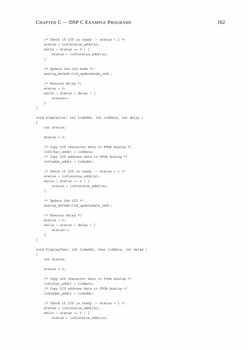
CHAPTER C — DSP C EXAMPLE PROGRAMS 162
/* Check if LCD is ready -- status = 1 */
status = lcd[status_addr]&1;
while ( status == 0 ) {
status = lcd[status_addr]&1;
}
/* Update the LCD mode */
analog_doCmd0(lcd_updatemode_cmd);
/* Execute delay */
status = 0;
while ( status < delay ) {
status++;
}
}
void DisplayInt( int lcdaddr, int lcddata, int delay )
{
int status;
status = 0;
/* Copy LCD character data to FPGA Analog */
lcd[char_addr] = lcddata;
/* Copy LCD address data to FPGA Analog */
lcd[addr_addr] = lcdaddr;
/* Check if LCD is ready -- status = 1 */
status = lcd[status_addr]&1;
while ( status == 0 ) {
status = lcd[status_addr]&1;
}
/* Update the LCD */
analog_doCmd0(lcd_updatedata_cmd);
/* Execute delay */
status = 0;
while ( status < delay ) {
status++;
}
}
void DisplayChar( int lcdaddr, char lcddata, int delay )
{
int status;
status = 0;
/* Copy LCD character data to FPGA Analog */
lcd[char_addr] = lcddata;
/* Copy LCD address data to FPGA Analog */
lcd[addr_addr] = lcdaddr;
/* Check if LCD is ready -- status = 1 */
status = lcd[status_addr]&1;
while ( status == 0 ) {
status = lcd[status_addr]&1;

CHAPTER C — DSP C EXAMPLE PROGRAMS 163
}
/* Update the LCD */
analog_doCmd0(lcd_updatedata_cmd);
/* Execute delay */
status = 0;
while ( status < delay ) {
status++;
}
}
void RTC_Write_Data( int addr, int data )
{
int delay;
int status;
/* Check if RTC is ready -- status = 1 */
status = rtc[rtc_status]&1;
while ( status != 1 ) {
status = rtc[rtc_status]&1;
}
/* Copy RTC data to FPGA Main */
*rtc_wr_data = data;
/* Copy address of RTC data to FPGA Main */
rtc[rtc_wr_addr] = addr;
/* Update RTC data */
main_doCmd0( 1 );
}
int RTC_Read_Data( int addr )
{
int data;
int status;
/* Check if RTC is ready -- status = 1 */
status = rtc[rtc_status]&1;
while ( status != 1 ) {
status = rtc[rtc_status]&1;
/*status++;*/
}
/* Get most recent RTC data from FPGA Main */
if ( ( addr <= 7 )&&( addr >= 0 ) ) {
data = rtc_rd_data[ addr ]&255;
}
else {
data = -1;
}
/* Return the data */
return data;
}
CHAPTER C — DSP C EXAMPLE PROGRAMS 164
main(void)
{
int i,j;
int pos;
unsigned int *prim_bus_ctrl = (unsigned int *)0x808064;
*prim_bus_ctrl = 0x10C8;
/* Disable interrupts */
asm(" OR 0h,IE");
asm(" OR 2000h,ST");
i = 0;
while (i<11250000) {
i++;
}
/* Initialize the LCD */
Mode( 0x30, 3075000 );
Mode( 0x30, 750000 );
Mode( 0x30, 0 );
Mode( 0x3C, 0 );
Mode( 0x0C, 0 );
Mode( 0x01, 0 );
Mode( 0x06, 0 );
i = 0;
while (i<150000) {
i++;
}
/* Output ’HALLO WORLD!’ on LCD */
DisplayChar( 0, ’ ’, 0 ); /* dummy character */
DisplayChar( 0, ’H’, 0 );
DisplayChar( 1, ’A’, 0 );
DisplayChar( 2, ’L’, 0 );
DisplayChar( 3, ’L’, 0 );
DisplayChar( 4, ’O’, 0 );
DisplayChar( 5, ’ ’, 0 );
DisplayChar( 6, ’W’, 0 );
DisplayChar( 7, ’O’, 0 );
DisplayChar( 8, ’R’, 0 );
DisplayChar( 9, ’L’, 0 );
DisplayChar( 10, ’D’, 0 );

CHAPTER C — DSP C EXAMPLE PROGRAMS 165
DisplayChar( 11, ’!’, 30000000 );
/* Clear the LCD */
Mode( 0x01, 0 );
/* Set RTC seconds = 30 */
RTC_Write_Data( 0, 0x30 );
/* Enable RTC square wave output ( 1Hz ) */
RTC_Write_Data( 7, 0x10 );
/* Set RTC minutes = 59 */
RTC_Write_Data( 1, 0x59 );
/* Set RTC hours = 23 */
RTC_Write_Data( 2, 0x23 );
/* Set RTC day = 7 */
RTC_Write_Data( 3, 0x07 );
/* Set RTC date = 31 */
RTC_Write_Data( 4, 0x31 );
/* Set RTC month = 12 */
RTC_Write_Data( 5, 0x12 );
/* Set RTC year = 99 */
RTC_Write_Data( 6, 0x99 );
j = 0;
while ( 1 ) {
/* Wait before updating LCD */
i = 0;
while (i<100000) {
i++;
}
/* Read the hours */
hr = RTC_Read_Data( 2 );
/* Read the minutes */
min = RTC_Read_Data( 1 );
/* Read the seconds */
sec = RTC_Read_Data( 0 );
ls_hr = (hr&0x0F) + 0x30;
ms_hr = ((hr&0x30)>>4) + 0x30 ;
ls_min = (min&0x0F) + 0x30;
ms_min = ((min&0x70)>>4) + 0x30;
ls_sec = (sec&0x0F) + 0x30;
ms_sec = ((sec&0x70)>>4) + 0x30;
DisplayChar( 0x00, ’ ’, 0x00 ); /* dummy character */
DisplayInt( 0x00, ms_hr, 0x00 );
DisplayInt( 0x01, ls_hr, 0x00 );

CHAPTER C — DSP C EXAMPLE PROGRAMS 166
DisplayInt( 0x03, ms_min, 0x00 );
DisplayInt( 0x04, ls_min, 0x00 );
DisplayInt( 0x06, ms_sec, 0x00 );
DisplayInt( 0x07, ls_sec, 0x00 );
}
}
C.5 The DSP C Program Implementing the Active Power
Filter’s Control Algorithm#include <string.h>
#include <math.h>
#include <stdlib.h>
#include <float.h>
#include <limits.h>
#include "Address2.h"
asm(" .sect \"vectors\" ");
asm(" BU _int0 ");
asm(" NOP ");
asm(" BU _int2 ");
#define p_limit 50
#define trimax 750
float pi = 3.141592654;
float pos_tan60 = 1.73205;
float neg_tan60 = -1.73205;
float inv_Vd = 0.005;
float L = 0.002;
float Ts = 0.0002;
unsigned int probe;
unsigned int sector;
float Delta;
float invDelta;
float LdivTs;
float Iconv_Alfa_Ref, Iconv_Beta_Ref;
float V_Alfa_Ref, V_Beta_Ref;
float p, p_ac, p_tot, q, p_mean;
float V_A, V_B, V_C;
float I_A, I_B, I_C;
float Iconv_A, Iconv_B, Iconv_C;

CHAPTER C — DSP C EXAMPLE PROGRAMS 167
float V_Alfa, V_Beta;
float I_Alfa, I_Beta;
float Iconv_Alfa, Iconv_Beta;
float D_A, D_B, D_C;
float Ref_A, Ref_B, Ref_C;
unsigned int state;
unsigned int data_rdy;
unsigned int compute_new_refs;
unsigned int update_refs;
unsigned int cmd1_mask;
unsigned int adc0_data, adc0_chan;
unsigned int adc1_data, adc1_chan;
unsigned int adc2_data, adc2_chan;
unsigned int adc0_data0, adc0_data1, adc0_data2;
unsigned int adc1_data0, adc1_data1, adc1_data2;
unsigned int adc2_data0, adc2_data1, adc2_data2;
int offset_adc0_data0, offset_adc0_data1, offset_adc0_data2;
int offset_adc1_data0, offset_adc1_data1, offset_adc1_data2;
int offset_adc2_data0, offset_adc2_data1, offset_adc2_data2;
void doCmd0( int cmd )
{
int i;
*analog_cmd0 = cmd;
i = 0;
while ( i < 1 ) i++;
*analog_cmd0 = 0;
}
void doCmd1( int cmd )
{
int i;
*analog_cmd1 = cmd;
i = 0;
while ( i < 1 ) i++;
}
void ClarkeTransform( float Phase_A, float Phase_B, float Phase_C,
float *Alfa, float *Beta )
{
*Alfa = 0.816497*(Phase_A - 0.5*Phase_B - 0.5*Phase_C);
*Beta = 0.816497*(0.866025*Phase_B - 0.866025*Phase_C);
}
void InvClarkeTransform( float Alfa, float Beta, float *Phase_A,
float *Phase_B, float *Phase_C )
{
*Phase_A = 0.816497*(Alfa);
*Phase_B = 0.816497*(-0.5*Alfa + 0.866025*Beta);
*Phase_C = 0.816497*(-0.5*Alfa - 0.866025*Beta);
}
CHAPTER C — DSP C EXAMPLE PROGRAMS 168
unsigned int ComputeSector( float U_Alfa_Ref, float U_Beta_Ref )
{
int CS_sector;
if ( U_Beta_Ref >= 0.0 )
{
if ( U_Beta_Ref >= pos_tan60*abs(U_Alfa_Ref) )
{
CS_sector = 2;
}
else
if ( U_Alfa_Ref >= 0.0 )
{
CS_sector = 1;
}
else CS_sector = 3;
}
else
if ( U_Beta_Ref <= neg_tan60*abs(U_Alfa_Ref) )
{
CS_sector = 5;
}
else
if ( U_Alfa_Ref >= 0.0 )
{
CS_sector = 6;
}
else CS_sector = 4;
return CS_sector;
}
void ComputeDutyCycles( int CDS_sector, float U_Alfa_Ref, float U_Beta_Ref,
float *D_A, float *D_B, float *D_C )
{
float d1_, d2_, d3_, d4_, d5_, d6_;
float d0, d1, d2, d3, d4, d5, d6;
probe = 0;
if ( CDS_sector == 1 )
{
d1_ = inv_Vd*(1.225*U_Alfa_Ref - 0.7071*U_Beta_Ref);
d2_ = inv_Vd*( 1.414*U_Beta_Ref);
if ( d1_ + d2_ < 1.0 )
{
d1 = d1_;
d2 = d2_;
d0 = 1.0 - (d1_ + d2_);
}
else
{
d1 = d1_/(d1_+d2_);
d2 = 1.0 - d1;
d0 = 0.0;
}

CHAPTER C — DSP C EXAMPLE PROGRAMS 169
*D_A = 0.5*d0 + d1 + d2;
*D_B = 0.5*d0 + d2;
*D_C = 0.5*d0;
probe = 1;
}
else if ( CDS_sector == 2 )
{
d2_ = inv_Vd*(1.225*U_Alfa_Ref + 0.7071*U_Beta_Ref);
d3_ = inv_Vd*(-1.225*U_Alfa_Ref + 0.7071*U_Beta_Ref);
if ( d2_ + d3_ < 1.0 )
{
d2 = d2_;
d3 = d3_;
d0 = 1.0 - (d2_ + d3_);
}
else
{
d2 = d2_/(d2_+d3_);
d3 = 1.0 - d2;
d0 = 0.0;
}
*D_A = 0.5*d0 + d2;
*D_B = 0.5*d0 + d2 + d3;
*D_C = 0.5*d0;
probe = 2;
}
else if ( CDS_sector == 3 )
{
d3_ = inv_Vd*( 1.414*U_Beta_Ref);
d4_ = inv_Vd*(-1.225*U_Alfa_Ref - 0.7071*U_Beta_Ref);
if ( d3_ + d4_ < 1.0 )
{
d3 = d3_;
d4 = d4_;
d0 = 1.0 - (d3_ + d4_);
}
else
{
d3 = d3_/(d3_+d4_);
d4 = 1.0 - d3;
d0 = 0.0;
}
*D_A = 0.5*d0;
*D_B = 0.5*d0 + d3 + d4;
*D_C = 0.5*d0 + d4;
probe = 3;
}
else if ( CDS_sector == 4 )
{
d4_ = inv_Vd*(-1.225*U_Alfa_Ref + 0.7071*U_Beta_Ref);
d5_ = inv_Vd*(-1.414*U_Beta_Ref);

CHAPTER C — DSP C EXAMPLE PROGRAMS 170
if ( d4_ + d5_ < 1.0 )
{
d4 = d4_;
d5 = d5_;
d0 = 1.0 - (d4_ + d5_);
}
else
{
d4 = d4_/(d4_+d5_);
d5 = 1.0 - d4;
d0 = 0.0;
}
*D_A = 0.5*d0;
*D_B = 0.5*d0 + d4;
*D_C = 0.5*d0 + d4 + d5;
probe = 4;
}
else if ( CDS_sector == 5 )
{
d5_ = inv_Vd*(-1.225*U_Alfa_Ref - 0.7071*U_Beta_Ref);
d6_ = inv_Vd*( 1.225*U_Alfa_Ref - 0.7071*U_Beta_Ref);
if ( d5_ + d6_ < 1.0 )
{
d5 = d5_;
d6 = d6_;
d0 = 1.0 - (d5_ + d6_);
}
else
{
d5 = d5_/(d5_+d6_);
d6 = 1.0 - d5;
d0 = 0.0;
}
*D_A = 0.5*d0 + d6;
*D_B = 0.5*d0;
*D_C = 0.5*d0 + d5 + d6;
probe = 5;
}
else if ( CDS_sector == 6 )
{
d6_ = inv_Vd*(-1.414*U_Beta_Ref);
d1_ = inv_Vd*( 1.225*U_Alfa_Ref + 0.7071*U_Beta_Ref);
if ( d6_ + d1_ < 1.0 )
{
d6 = d6_;
d1 = d1_;
d0 = 1.0 - (d6_ + d1_);
}
else
{
d6 = d6_/(d6_+d1_);
d1 = 1.0 - d6;

CHAPTER C — DSP C EXAMPLE PROGRAMS 171
d0 = 0.0;
}
*D_A = 0.5*d0 + d6 + d1;
*D_B = 0.5*d0;
*D_C = 0.5*d0 + d6;
probe = 6;
}
}
void Mode( int mode, int delay )
{
int status;
status = 0;
lcd[mode_addr] = mode;
while ( status < 1000000 ) {
status++;
}
doCmd0(lcd_updatemode_cmd);
status = 0;
while ( status < delay ) {
status++;
}
}
void Display( int lcdaddr, int lcddata, int delay )
{
int status;
status = 0;
lcd[char_addr] = lcddata;
lcd[addr_addr] = lcdaddr;
while ( status < 5000 ) {
status++;
}
doCmd0(lcd_updatedata_cmd);
status = 0;
while ( status < 5000 ) {
status++;
}
doCmd0(lcd_updatedata_cmd);
status = 0;
while ( status < delay ) {
status++;
}
}
interrupt void int2(void)
{
/* unsigned int keypressed;*/
CHAPTER C — DSP C EXAMPLE PROGRAMS 172
unsigned int int_reg;
asm(" AND 0h,IE");
asm(" AND 0FFFFFFFBh,IF");
dac0[b_data_addr] = 2048;
doCmd0( dac0_load_cmd );
int_reg = (*fpganlg_int_reg)&63;
asm(" OR 1h,IE");
asm(" AND 0FFFFFFFBh,IF");
}
interrupt void int0(void)
{
/*unsigned int adc_data, adc_chan; */
unsigned int int_reg;
unsigned int adc_status_reg;
unsigned int keypressed;
unsigned int temp0;
unsigned int temp1;
unsigned int temp2;
unsigned int temp_cntr;
asm(" AND 0h,IE");
asm(" AND 0FFFFFFFEh,IF");
int_reg = (*fpganlg_int_reg)&63;
if ((int_reg&16)==16) /* PWM block 0 event occured ? */
{
if (state == 0)
{
compute_new_refs = 1;
}
else if ( state == 2 )
{
update_refs = 1;
}
*fpganlg_int_en = 0x0007;
}
if ((int_reg&2)==2) /* A key was pressed ? */
{
keypressed = (unsigned int)((*keyval)&15);
if ( keypressed == 10 ) {
keypressed = keypressed + 0x26;
}
else if ( keypressed == 11 ) {
keypressed = keypressed + 0x1F;
}
else if ( keypressed == 12 ) {
keypressed = keypressed + 0x17;
}
else keypressed = keypressed + 0x30;

CHAPTER C — DSP C EXAMPLE PROGRAMS 173
Display( 0x0D, keypressed, 0x00 );
*fpganlg_int_en = 0x0007;
}
if ((int_reg&1)==1)
{
*fpganlg_int_en = 0x0000;
temp0 = (unsigned int)((adc0[adc_data_addr])&8191);
temp1 = (unsigned int)((adc1[adc_data_addr])&8191);
temp2 = (unsigned int)((adc2[adc_data_addr])&8191);
adc0_data = (unsigned int)( temp0&1023 );
adc0_chan = (unsigned int)( (temp0&7168) >> 10 );
adc1_data = (unsigned int)( temp1&1023 );
adc1_chan = (unsigned int)( (temp1&7168) >> 10 );
adc2_data = (unsigned int)( temp2&1023 );
adc2_chan = (unsigned int)( (temp2&7168) >> 10 );
if (adc0_chan==0)
{
adc0_data0 = adc0_data;
}
else
{
if (adc0_chan==1)
{
adc0_data1 = adc0_data;
}
else
{
if (adc0_chan==2)
{
adc0_data2 = adc0_data;
}
}
}
if (adc1_chan==0)
{
adc1_data0 = adc1_data;
}
else
{
if (adc1_chan==1)
{
adc1_data1 = adc1_data;
}
else
{
if (adc1_chan==2)
{
adc1_data2 = adc1_data;
}
}

CHAPTER C — DSP C EXAMPLE PROGRAMS 174
}
if (adc2_chan==0)
{
adc2_data0 = adc2_data;
}
else
{
if (adc2_chan==1)
{
adc2_data1 = adc2_data;
}
else
{
if (adc2_chan==2)
{
adc2_data2 = adc2_data;
}
}
}
*fpganlg_int_en = 0x0107;
}
asm(" OR 1h,IE");
asm(" AND 0FFFFFFFEh,IF");
}
main(void)
{
unsigned int pwmstatus;
int i,j,k,l;
int pos, dir;
unsigned int toggle;
float old_Iconv_A, old_Iconv_B, old_Iconv_C;
float delta_Iconv;
float q_old;
int p_num;
float p_arr[p_limit];
unsigned int *prim_bus_ctrl = (unsigned int *)0x808064;
*prim_bus_ctrl = 0x10F8;
*fpganlg_int_en = 0x0000;
LdivTs = L/Ts;
Ts = 0.0002;
toggle = 0;

CHAPTER C — DSP C EXAMPLE PROGRAMS 175
cmd1_mask = 0;
data_rdy = 0;
compute_new_refs = 0;
asm(" OR 1h,IE");
asm(" OR 2000h,ST");
asm(" AND 0FFFFFFFEh,IF");
adc0[adc_samp_chan0_addr] = 0;
adc0[adc_samp_chan1_addr] = 1;
adc0[adc_samp_chan2_addr] = 2;
adc0[adc_samp_chan3_addr] = 1;
adc0[adc_samp_chan4_addr] = 0;
adc0[adc_samp_chan5_addr] = 1;
adc0[adc_samp_chan6_addr] = 2;
adc0[adc_samp_chan7_addr] = 1;
adc1[adc_samp_chan0_addr] = 0;
adc1[adc_samp_chan1_addr] = 1;
adc1[adc_samp_chan2_addr] = 2;
adc1[adc_samp_chan3_addr] = 1;
adc1[adc_samp_chan4_addr] = 0;
adc1[adc_samp_chan5_addr] = 1;
adc1[adc_samp_chan6_addr] = 2;
adc1[adc_samp_chan7_addr] = 1;
adc2[adc_samp_chan0_addr] = 0;
adc2[adc_samp_chan1_addr] = 1;
adc2[adc_samp_chan2_addr] = 2;
adc2[adc_samp_chan3_addr] = 1;
adc2[adc_samp_chan4_addr] = 0;
adc2[adc_samp_chan5_addr] = 1;
adc2[adc_samp_chan6_addr] = 2;
adc2[adc_samp_chan7_addr] = 1;
adc0[adc_conf_addr] = 0x0000;
adc1[adc_conf_addr] = 0x0000;
adc2[adc_conf_addr] = 0x0000;
pwm0[pwm_trimax_addr] = trimax;
pwm0[pwm_trifreqscale_addr] = 1;
pwm0[pwm_deadtime_addr] = 60;
pwm0[pwm_upval_addr] = 1023;
pwm0[pwm_downval_addr] = 120;
pwm0[pwm_refa_addr] = trimax/2;
pwm0[pwm_refb_addr] = trimax/2;
pwm0[pwm_refc_addr] = trimax/2;
pwm0[pwm_refn_addr] = trimax/2;
dac0[ctrl_addr] = 3;
dac0[a_conf_addr] = 4;
dac0[b_conf_addr] = 4;
i = 0;
while (i<11250000) {
i++;

CHAPTER C — DSP C EXAMPLE PROGRAMS 176
}
Mode( 0x30, 3075000 );
Mode( 0x30, 750000 );
Mode( 0x30, 0 );
Mode( 0x3C, 0 );
Mode( 0x0C, 0 );
Mode( 0x01, 0 );
Mode( 0x06, 0 );
Display( 0x00, 0xFF, 0x00 );
i = 0;
while (i<150000) {
i++;
}
/* Display "HALLO WORLD!" on LCD */
Display( 0x00, 0x48, 0x00 );
Display( 0x01, 0x61, 0x00 );
Display( 0x02, 0x6C, 0x00 );
Display( 0x03, 0x6C, 0x00 );
Display( 0x04, 0x6F, 0x00 );
Display( 0x05, 0x20, 0x00 );
Display( 0x06, 0x57, 0x00 );
Display( 0x07, 0x6F, 0x00 );
Display( 0x08, 0x72, 0x00 );
Display( 0x09, 0x6C, 0x00 );
Display( 0x0A, 0x64, 0x00 );
Display( 0x0B, 0x21, 0x00 );
p_num = 0;
p_tot = 0.0;
while (p_num < p_limit)
{
p_arr[p_num] = 0.0;
++p_num;
}
p_num = 0;
adc0_data0 = 0;
adc0_data1 = 0;
adc0_data2 = 0;
adc1_data0 = 0;
adc1_data1 = 0;
adc1_data2 = 0;
adc2_data0 = 0;
adc2_data1 = 0;
adc2_data2 = 0;
offset_adc0_data0 = 0;
offset_adc0_data1 = 0;
offset_adc0_data2 = 0;

CHAPTER C — DSP C EXAMPLE PROGRAMS 177
offset_adc1_data0 = 0;
offset_adc1_data1 = 0;
offset_adc1_data2 = 0;
offset_adc2_data0 = 0;
offset_adc2_data1 = 0;
offset_adc2_data2 = 0;
doCmd1(adc0_en_cmd+adc1_en_cmd+adc2_en_cmd);
i = 0;
while (i<1000000) {
*fpganlg_int_en = 0x0107;
offset_adc0_data0 = offset_adc0_data0 + adc0_data0;
offset_adc0_data1 = offset_adc0_data1 + adc0_data1;
offset_adc0_data2 = offset_adc0_data2 + adc0_data2;
offset_adc1_data0 = offset_adc1_data0 + adc1_data0;
offset_adc1_data1 = offset_adc1_data1 + adc1_data1;
offset_adc1_data2 = offset_adc1_data2 + adc1_data2;
offset_adc2_data0 = offset_adc2_data0 + adc2_data0;
offset_adc2_data1 = offset_adc2_data1 + adc2_data1;
offset_adc2_data2 = offset_adc2_data2 + adc2_data2;
i++;
}
offset_adc0_data0 = 512 - (offset_adc0_data0/i);
offset_adc0_data1 = 512 - (offset_adc0_data1/i);
offset_adc0_data2 = 625 - (offset_adc0_data2/i);
offset_adc1_data0 = 512 - (offset_adc1_data0/i);
offset_adc1_data1 = 512 - (offset_adc1_data1/i);
offset_adc1_data2 = 625 - (offset_adc1_data2/i);
offset_adc2_data0 = 512 - (offset_adc2_data0/i);
offset_adc2_data1 = 512 - (offset_adc2_data1/i);
offset_adc2_data2 = 625 - (offset_adc2_data2/i);
doCmd1(adc0_en_cmd+adc1_en_cmd+adc2_en_cmd+pwm0_en_cmd);
dir = 1;
pos = 1;
while ( 1 ) {
state = 0;
compute_new_refs = 0;
*fpganlg_int_en = 0x0107;
/* wait until compare down value trigger */
while (compute_new_refs == 0)
{
}
*fpganlg_int_en = 0x0000;
state = 1;

CHAPTER C — DSP C EXAMPLE PROGRAMS 178
asm(" AND 0h,IE");
asm(" AND 0FFFFFFFEh,IF");
V_A = (float)(-0.3125*(float)(adc0_data0+offset_adc0_data0) + 160.0);
V_B = (float)(-0.3125*(float)(adc1_data0+offset_adc1_data0) + 160.0);
V_C = (float)(-0.3125*(float)(adc2_data0+offset_adc2_data0) + 160.0);
I_A = (float)(-0.019531*(float)(adc0_data1+offset_adc0_data1) + 10.0);
I_B = (float)(-0.019531*(float)(adc1_data1+offset_adc1_data1) + 10.0);
I_C = (float)(-0.019531*(float)(adc2_data1+offset_adc2_data1) + 10.0);
Iconv_A = (float)(0.0533*(float)(adc0_data2+offset_adc0_data2) - 33.3);
Iconv_B = (float)(0.0533*(float)(adc1_data2+offset_adc1_data2) - 33.3);
Iconv_C = (float)(0.0533*(float)(adc2_data2+offset_adc2_data2) - 33.3);
ClarkeTransform( V_A, V_B, V_C, &V_Alfa, &V_Beta );
ClarkeTransform( I_A, I_B, I_C, &I_Alfa, &I_Beta );
ClarkeTransform( Iconv_A, Iconv_B, Iconv_C, &Iconv_Alfa, &Iconv_Beta );
p = (float)(I_Alfa*V_Alfa + I_Beta*V_Beta);
q = (float)(-I_Alfa*V_Beta + I_Beta*V_Alfa);
/* Create circular buffer of power values to compute average power */
p_tot = p_tot - p_arr[p_num]; /* Subtract oldest value from sum of power values */
p_arr[p_num] = p; /* Insert the new value in the array */
p_tot = p_tot + p; /* Add new value to the value for the total power */
p_mean = p_tot/p_limit; /* Compute the average power */
p_ac = p - p_mean; /* Compute the AC component of the power */
if (p_num < p_limit) /* Move pointer to next value’s location */
{
++p_num;
}
else
{
p_num = 0;
}
Delta = V_Alfa*V_Alfa + V_Beta*V_Beta;
if (Delta == 0.0)
{
Delta = 0.000001;
}
invDelta = (float)((1.0)/((float)Delta));
Iconv_Alfa_Ref = (float)((V_Alfa*p_ac - V_Beta*q)*invDelta);
Iconv_Beta_Ref = (float)((V_Beta*p_ac + V_Alfa*q)*invDelta);
V_Alfa_Ref = (float)( LdivTs*(Iconv_Alfa_Ref - Iconv_Alfa) + V_Alfa );
V_Beta_Ref = (float)( LdivTs*(Iconv_Beta_Ref - Iconv_Beta) + V_Beta );
sector = ComputeSector(V_Alfa_Ref, V_Beta_Ref);
ComputeDutyCycles( sector, V_Alfa_Ref, V_Beta_Ref, &D_A, &D_B, &D_C );
Ref_A = (float)(trimax*( D_A ));
Ref_B = (float)(trimax*( D_B ));
Ref_C = (float)(trimax*( D_C ));
CHAPTER C — DSP C EXAMPLE PROGRAMS 179
asm(" OR 1h,IE");
asm(" OR 2000h,ST");
asm(" AND 0FFFFFFFEh,IF");
state = 2;
update_refs = 0;
*fpganlg_int_en = 0x0400;
/* wait until counterzero trigger */
while (update_refs == 0)
{
}
*fpganlg_int_en = 0x0007;
pwm0[pwm_refa_addr] = (unsigned int)Ref_A;
pwm0[pwm_refb_addr] = (unsigned int)Ref_B;
pwm0[pwm_refc_addr] = (unsigned int)Ref_C;
dac0[a_data_addr] = (unsigned int)(256*I_A+2048);
dac0[b_data_addr] = (unsigned int)(12.7*q+2048);
doCmd0( dac0_load_cmd );
}
}

Appendix D
PLD Firmware
D.1 Firmware for FPGA Main
180

CHAPTER D — PLD FIRMWARE 181
D.1.1 Graphical Design File for FPGA Main
GLOBAL_RESETDSP_H1
RTC_RD_DATA[63..0]
CMD_REG1_ENCMD_REG0_ENRTC_RD_DATA_EN[7..0] DATA[15..0]
RTC_RDYnBSY
RTC_WR_DATA_ENRTC_WR_ADDR_ENRTC_STATUS_EN
RTC_WR_ADDR[7..0]
CMD_REG1[7..0]CMD_REG0[7..0]RTC_WR_DATA[7..0]
FRAM_STATUS_EN
SERIAL_BAUD_ENSERIAL_STATUS_ENSERIAL_STATUS[1..0]
SP_BAUDRATE[2..0]
FRAM_STATUS[1..0]
CMD_REG1[7..0]
GLOBAL_CLKGLOBAL_RESET
CMD_REG0[7..0]RTC_WR_nEN
CMD_REG1_EN
GLOBAL_RESETDSP_H1
CMD_REG0_ENRTC_RD_DATA_EN[7..0]
RTC_WR_ADDR_ENRTC_WR_DATA_EN
FPGAMAIN_nCS
ADDR[9..0]
RTC_STATUS_EN
SERIAL_RX_DATA_ENSERIAL_STATUS_ENSERIAL_BAUD_EN
SERIAL_TX_DATA_ENFRAM_STATUS_EN
ADDR[9..0]
pec33_main_ver3@55DATA13BIDIR
pec33_main_ver3@54DATA14BIDIR
pec33_main_ver3@53DATA15BIDIR
pec33_main_ver3@60DATA9BIDIR
pec33_main_ver3@58DATA10BIDIR
pec33_main_ver3@56DATA12BIDIRpec33_main_ver3@57DATA11BIDIR
pec33_main_ver3@65DATA5BIDIR
pec33_main_ver3@64DATA6BIDIR
pec33_main_ver3@61DATA8BIDIRpec33_main_ver3@63DATA7BIDIR
pec33_main_ver3@180 nRESET INPUT
pec33_main_ver3@79 GLOBAL_CLK INPUT
NOT pec33_main_ver3@70DATA1BIDIR
pec33_main_ver3@69DATA2BIDIR
pec33_main_ver3@67DATA4BIDIRpec33_main_ver3@68DATA3BIDIR
pec33_main_ver3@71DATA0BIDIR
pec33_main_ver3@139 DSP_nSTRB INPUT
pec33_main_ver3@112 ADDR19 INPUT
pec33_main_ver3@102 ADDR15 INPUT
pec33_main_ver3@111 ADDR18 INPUT
pec33_main_ver3@103 ADDR16 INPUT
pec33_main_ver3@104 ADDR17 INPUT
pec33_main_ver3@97 ADDR11 INPUT
pec33_main_ver3@101 ADDR14 INPUT
pec33_main_ver3@99 ADDR12 INPUT
pec33_main_ver3@100 ADDR13 INPUT
pec33_main_ver3@93 ADDR7 INPUT
pec33_main_ver3@96 ADDR10 INPUT
pec33_main_ver3@94 ADDR8 INPUT
pec33_main_ver3@95 ADDR9 INPUT
pec33_main_ver3@88 ADDR3 INPUT
pec33_main_ver3@92 ADDR6 INPUT
pec33_main_ver3@89 ADDR4 INPUT
pec33_main_ver3@90 ADDR5 INPUT
pec33_main_ver3@87 ADDR2 INPUT
pec33_main_ver3@85 ADDR0 INPUT
pec33_main_ver3@86 ADDR1 INPUT
Figure D.1: Graphical Design File of FPGA Main (Part 1 of 3)
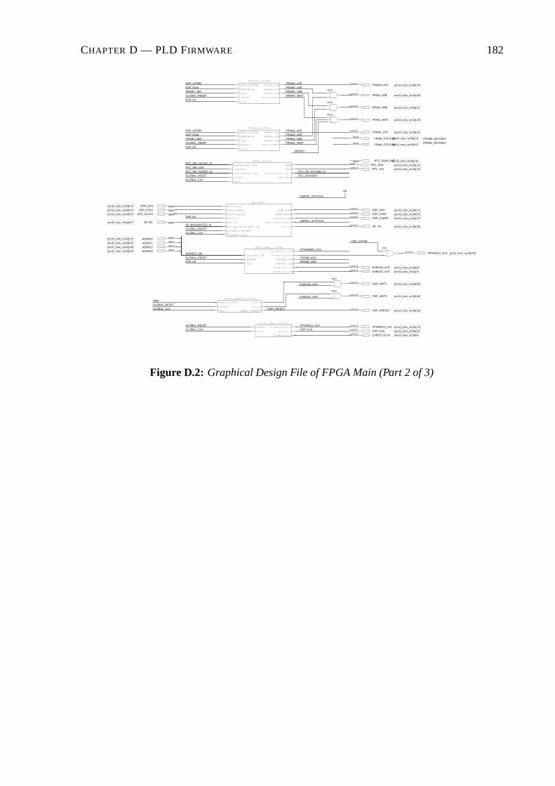
CHAPTER D — PLD FIRMWARE 182
GLOBAL_RESETGLOBAL_CLK
FPGANLG_CLKDSP_CLK
GLOBAL_CLK DSP_nRESET
DIP0GLOBAL_RESET
EXBUS1_nINT
EXBUS0_nINT
GLOBAL_RESETDSP_H1
FRAM0_nENFRAM1_nEN
ADDR[23..20]FPGAMAIN_nCS
DSP_nSTRB
SP_BAUDRATE[2..0]GLOBAL_RESETGLOBAL_CLK
DSP_H1SERIAL_STATUS0
SERIAL_STATUS1
GLOBAL_CLKGLOBAL_RESET RTC_RDYnBSY
RTC_WR_nENRTC_WR_DATA[7..0]
RTC_WR_ADDR[7..0] RTC_RD_DATA[63..0]
DSP_H1GLOBAL_RESET FRAM1_nRST
nRESET
FRAM1_nENDSP_RnWDSP_nSTRB
FRAM1_nOEFRAM1_nCE
FRAM1_nWE
GLOBAL_RESETDSP_H1
FRAM0_nRST
DSP_nSTRBDSP_RnWFRAM0_nEN
FRAM0_nCEFRAM0_nOEFRAM0_nWE
FRAM1_RDYnBSYFRAM0_RDYnBSY
pec33_main_ver3@157DSP_CLKOUTPUTpec33_main_ver3@179FPGANLG_CLKOUTPUT
pec33_main_ver3@41EXBUS_GCLKOUTPUT
pec33_main_ver3@159DSP_nRESETOUTPUT
AND2
pec33_main_ver3@166DSP_nINT3OUTPUT
AND2
pec33_main_ver3@164DSP_nINT1OUTPUT
pec33_main_ver3@45EXBUS0_nCSOUTPUT
pec33_main_ver3@75EXBUS1_nCSOUTPUT
pec33_main_ver3@147 ADDR21 INPUT
pec33_main_ver3@148 ADDR22 INPUT
pec33_main_ver3@149 ADDR23 INPUTOR2
pec33_main_ver3@189FPGANLG_nCSOUTPUT
pec33_main_ver3@113 ADDR20 INPUT
pec33_main_ver3@196SP_TXOUTPUT
pec33_main_ver3@173 DSP_FSX0 INPUT
pec33_main_ver3@174 DSP_CLKX0 INPUT
pec33_main_ver3@197 SP_RX INPUT
pec33_main_ver3@176DSP_FSR0OUTPUT
pec33_main_ver3@175DSP_CLKR0OUTPUT
pec33_main_ver3@177DSP_DR0OUTPUTpec33_main_ver3@172 DSP_DX0 INPUT
VCC
pec33_main_ver3@114RTC_SDABIDIRpec33_main_ver3@116RTC_SQW_OUTINPUT
pec33_main_ver3@115RTC_SCLOUTPUT
pec33_main_ver3@121FRAM_STATUS1INPUT
pec33_main_ver3@120FRAM_STATUS0INPUT
pec33_main_ver3@122FRAM1_nCEOUTPUT
AND2
AND3
pec33_main_ver3@128FRAM_nRSTOUTPUT
AND2
pec33_main_ver3@126FRAM_nOEOUTPUT
pec33_main_ver3@127FRAM_nWEOUTPUT
pec33_main_ver3@125FRAM0_nCEOUTPUT
Figure D.2: Graphical Design File of FPGA Main (Part 2 of 3)
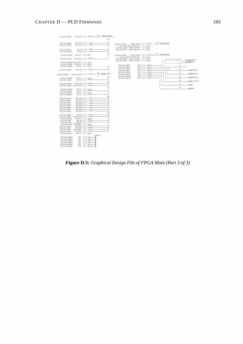
CHAPTER D — PLD FIRMWARE 183
SP_RX
DSP_DR0
SP_BAUDRATE2
SERIAL_STATUS0
GLOBAL_RESET SP_BAUDRATE1
SP_BAUDRATE0
GLOBAL_CLK
GLOBAL_RESET
GLOBAL_RESET
GLOBAL_RESET
FRAM_STATUS0
DIP[5..0]
pec33_main_ver3@205 DIP3 INPUT
pec33_main_ver3@207 DIP5 INPUT
pec33_main_ver3@206 DIP4 INPUT
pec33_main_ver3@204 DIP2 INPUT
pec33_main_ver3@203 DIP1 INPUT
pec33_main_ver3@202 DIP0 INPUT
pec33_main_ver3@11 USB_nEOT OUTPUT
pec33_main_ver3@13 USB_XTAL1 OUTPUTpec33_main_ver3@12 USB_nRESET OUTPUT
pec33_main_ver3@14 USB_A0 INPUT
pec33_main_ver3@7 USB_nRD OUTPUT
pec33_main_ver3@10 USB_DMACK OUTPUT
pec33_main_ver3@8 USB_nWR OUTPUT
pec33_main_ver3@9 USB_DMREQ INPUT
pec33_main_ver3@24 USB_SUSPEND BIDIRpec33_main_ver3@19 USB_nCS OUTPUT
pec33_main_ver3@25 USB_nINT INPUT
VCC
pec33_main_ver3@29 USB_DATA4 BIDIR
pec33_main_ver3@26 USB_DATA7 BIDIRpec33_main_ver3@27 USB_DATA6 BIDIRpec33_main_ver3@28 USB_DATA5 BIDIR
pec33_main_ver3@15 USB_DATA0 BIDIR
pec33_main_ver3@18 USB_DATA3 BIDIRpec33_main_ver3@17 USB_DATA2 BIDIRpec33_main_ver3@16 USB_DATA1 BIDIR
pec33_main_ver3@190 OP0_TX OUTPUT
pec33_main_ver3@192 OP1_TX OUTPUTpec33_main_ver3@193 OP1_RX INPUT
VCC
pec33_main_ver3@195 RS232_nEN OUTPUT
pec33_main_ver3@198 RS232_nSHDN OUTPUT
pec33_main_ver3@191 OP0_RX INPUT
VCC
NOT
NOT
pec33_main_ver3@199 CPP_TX OUTPUTpec33_main_ver3@200 CPP_RX INPUT
VCC
VCCpec33_main_ver3@133 LED7 OUTPUTpec33_main_ver3@134 LED6 OUTPUT
NOT
NOT
pec33_main_ver3@187 FPGANLG_nRESET OUTPUT
pec33_main_ver3@158 DSP_nSHZ OUTPUT
NOT
pec33_main_ver3@37 LED3 OUTPUT
pec33_main_ver3@136 LED4 OUTPUT
pec33_main_ver3@135 LED5 OUTPUT
pec33_main_ver3@36 LED2 OUTPUTNOT
NOT
pec33_main_ver3@144 DSP_nHOLDA INPUT
pec33_main_ver3@141 DSP_nIACK INPUT
pec33_main_ver3@183 DSP_H1 INPUT VCC pec33_main_ver3@31 LED1 OUTPUTpec33_main_ver3@30 LED0 OUTPUT
NOT
pec33_main_ver3@143 DSP_nHOLD OUTPUT
pec33_main_ver3@140 DSP_RnW INPUTVCC
pec33_main_ver3@83 EXBUS1_nRESET OUTPUT
pec33_main_ver3@40 EXBUS1_nINTREQ INPUT
pec33_main_ver3@73 EXBUS1_RDYnBSY INPUT
pec33_main_ver3@74 EXBUS1_nINT INPUT
NOT
pec33_main_ver3@167 DSP_XF0 BIDIR
pec33_main_ver3@168 DSP_XF1 BIDIRpec33_main_ver3@47 EXBUS0_RDYnBSY INPUT
pec33_main_ver3@39 EXBUS0_nINTREQ INPUT
pec33_main_ver3@170 DSP_TCLK1 BIDIRpec33_main_ver3@169 DSP_TCLK0 BIDIR
VCC
pec33_main_ver3@44 EXBUS0_nRESET OUTPUT
pec33_main_ver3@46 EXBUS0_nINT INPUT
NOT
pec33_main_ver3@142 DSP_nRDY OUTPUTNOT
Figure D.3: Graphical Design File of FPGA Main (Part 3 of 3)

CHAPTER D — PLD FIRMWARE 184
D.1.2 VHDL Code for the Addr Dec Ctrl Module of FPGA Main-- PEC 33 FPGA Main - Address Decoder Controller 2002-11-07
LIBRARY ieee;
USE ieee.std_logic_1164.all;
USE ieee.std_logic_arith.all;
ENTITY Addr_Dec_Ctrl IS
PORT (
FRAM_STATUS_EN : OUT STD_LOGIC;
SERIAL_TX_DATA_EN : OUT STD_LOGIC;
SERIAL_RX_DATA_EN : OUT STD_LOGIC;
SERIAL_STATUS_EN : OUT STD_LOGIC;
SERIAL_BAUD_EN : OUT STD_LOGIC;
RTC_STATUS_EN : OUT STD_LOGIC;
RTC_WR_ADDR_EN : OUT STD_LOGIC;
RTC_WR_DATA_EN : OUT STD_LOGIC;
RTC_RD_DATA_EN : OUT STD_LOGIC_VECTOR ( 7 DOWNTO 0 );
CMD_REG0_EN : OUT STD_LOGIC;
CMD_REG1_EN : OUT STD_LOGIC;
ADDR : IN STD_LOGIC_VECTOR ( 9 DOWNTO 0 );
nSTRB : IN STD_LOGIC;
FPGA_nCS : IN STD_LOGIC;
RESET : IN STD_LOGIC;
CLK : IN STD_LOGIC
);
END Addr_Dec_Ctrl;
ARCHITECTURE a OF Addr_Dec_Ctrl IS
TYPE statetype IS ( state0, state1, state2, state3 );
CONSTANT serial_tx_data_addr : INTEGER := 0;
CONSTANT serial_rx_data_addr : INTEGER := 1;
CONSTANT serial_status_addr : INTEGER := 2;
CONSTANT serial_baud_addr : INTEGER := 3;
CONSTANT fram_status_addr : INTEGER := 8;
CONSTANT rtc_status_addr : INTEGER := 16;
CONSTANT rtc_wr_addr_addr : INTEGER := 17;
CONSTANT rtc_wr_data_addr : INTEGER := 18;
CONSTANT rtc_rd_data_addr : INTEGER := 19;
CONSTANT cmd_reg0_addr : INTEGER := 102;
CONSTANT cmd_reg1_addr : INTEGER := 103;
SIGNAL trig_SERIAL_TX_DATA_EN : STD_LOGIC;
SIGNAL trig_SERIAL_RX_DATA_EN : STD_LOGIC;

CHAPTER D — PLD FIRMWARE 185
SIGNAL trig_SERIAL_STATUS_EN : STD_LOGIC;
SIGNAL trig_SERIAL_BAUD_EN : STD_LOGIC;
SIGNAL trig_FRAM_STATUS_EN : STD_LOGIC;
SIGNAL trig_RTC_STATUS_EN : STD_LOGIC;
SIGNAL trig_RTC_WR_ADDR_EN : STD_LOGIC;
SIGNAL trig_RTC_WR_DATA_EN : STD_LOGIC;
SIGNAL trig_RTC_RD_DATA_EN : STD_LOGIC_VECTOR ( 7 DOWNTO 0 );
SIGNAL trig_CMD_REG0_EN : STD_LOGIC;
SIGNAL trig_CMD_REG1_EN : STD_LOGIC;
signal signal_ADDR : INTEGER RANGE 0 TO 1023;
COMPONENT addr_element
GENERIC (
INT_ADDR : INTEGER RANGE 0 TO 1023 := 0
);
PORT (
EN : OUT STD_LOGIC;
ADDR : IN INTEGER RANGE 0 TO 1023;
nCS : IN STD_LOGIC;
nSTRB : IN STD_LOGIC;
RESET : IN STD_LOGIC;
CLK : IN STD_LOGIC
);
END COMPONENT;
BEGIN
signal_ADDR <= CONV_INTEGER( UNSIGNED( ADDR ) );
------------------------------------------------------------------------------------------
serial_tx_data_en_map:
addr_element GENERIC MAP ( INT_ADDR => serial_tx_data_addr )
PORT MAP ( EN => SERIAL_TX_DATA_EN, ADDR => signal_ADDR,
nCS => FPGA_nCS, nSTRB => nSTRB,
RESET => RESET, CLK => CLK
);
serial_rx_data_en_map:
addr_element GENERIC MAP ( INT_ADDR => serial_rx_data_addr )
PORT MAP ( EN => SERIAL_RX_DATA_EN, ADDR => signal_ADDR,
nCS => FPGA_nCS, nSTRB => nSTRB,
RESET => RESET, CLK => CLK
);
serial_status_en_map:
addr_element GENERIC MAP ( INT_ADDR => serial_status_addr )
PORT MAP ( EN => SERIAL_STATUS_EN, ADDR => signal_ADDR,
nCS => FPGA_nCS, nSTRB => nSTRB,
RESET => RESET, CLK => CLK
);
CHAPTER D — PLD FIRMWARE 186
serial_baud_en_map:
addr_element GENERIC MAP ( INT_ADDR => serial_baud_addr )
PORT MAP ( EN => SERIAL_BAUD_EN, ADDR => signal_ADDR,
nCS => FPGA_nCS, nSTRB => nSTRB,
RESET => RESET, CLK => CLK
);
------------------------------------------------------------------------------------------
fram_status_en_map:
addr_element GENERIC MAP ( INT_ADDR => fram_status_addr )
PORT MAP ( EN => FRAM_STATUS_EN, ADDR => signal_ADDR,
nCS => FPGA_nCS, nSTRB => nSTRB,
RESET => RESET, CLK => CLK
);
------------------------------------------------------------------------------------------
rtc_status_en_map:
addr_element GENERIC MAP ( INT_ADDR => rtc_status_addr )
PORT MAP ( EN => RTC_STATUS_EN, ADDR => signal_ADDR,
nCS => FPGA_nCS, nSTRB => nSTRB,
RESET => RESET, CLK => CLK
);
rtc_wr_addr_en_map:
addr_element GENERIC MAP ( INT_ADDR => rtc_wr_addr_addr )
PORT MAP ( EN => RTC_WR_ADDR_EN, ADDR => signal_ADDR,
nCS => FPGA_nCS, nSTRB => nSTRB,
RESET => RESET, CLK => CLK
);
rtc_wr_data_en_map:
addr_element GENERIC MAP ( INT_ADDR => rtc_wr_data_addr )
PORT MAP ( EN => RTC_WR_DATA_EN, ADDR => signal_ADDR,
nCS => FPGA_nCS, nSTRB => nSTRB,
RESET => RESET, CLK => CLK
);
rtc_rd_data0_en_map:
addr_element GENERIC MAP ( INT_ADDR => rtc_rd_data_addr )
PORT MAP ( EN => RTC_RD_DATA_EN( 0 ), ADDR => signal_ADDR,
nCS => FPGA_nCS, nSTRB => nSTRB,
RESET => RESET, CLK => CLK
);
rtc_rd_data1_en_map:
addr_element GENERIC MAP ( INT_ADDR => ( rtc_rd_data_addr + 1) )
PORT MAP ( EN => RTC_RD_DATA_EN( 1 ), ADDR => signal_ADDR,
nCS => FPGA_nCS, nSTRB => nSTRB,
RESET => RESET, CLK => CLK
);
rtc_rd_data2_en_map:
addr_element GENERIC MAP ( INT_ADDR => ( rtc_rd_data_addr + 2) )
PORT MAP ( EN => RTC_RD_DATA_EN( 2 ), ADDR => signal_ADDR,
nCS => FPGA_nCS, nSTRB => nSTRB,
RESET => RESET, CLK => CLK

CHAPTER D — PLD FIRMWARE 187
);
rtc_rd_data3_en_map:
addr_element GENERIC MAP ( INT_ADDR => ( rtc_rd_data_addr + 3) )
PORT MAP ( EN => RTC_RD_DATA_EN( 3 ), ADDR => signal_ADDR,
nCS => FPGA_nCS, nSTRB => nSTRB,
RESET => RESET, CLK => CLK
);
rtc_rd_data4_en_map:
addr_element GENERIC MAP ( INT_ADDR => ( rtc_rd_data_addr + 4) )
PORT MAP ( EN => RTC_RD_DATA_EN( 4 ), ADDR => signal_ADDR,
nCS => FPGA_nCS, nSTRB => nSTRB,
RESET => RESET, CLK => CLK
);
rtc_rd_data5_en_map:
addr_element GENERIC MAP ( INT_ADDR => ( rtc_rd_data_addr + 5) )
PORT MAP ( EN => RTC_RD_DATA_EN( 5 ), ADDR => signal_ADDR,
nCS => FPGA_nCS, nSTRB => nSTRB,
RESET => RESET, CLK => CLK
);
rtc_rd_data6_en_map:
addr_element GENERIC MAP ( INT_ADDR => ( rtc_rd_data_addr + 6) )
PORT MAP ( EN => RTC_RD_DATA_EN( 6 ), ADDR => signal_ADDR,
nCS => FPGA_nCS, nSTRB => nSTRB,
RESET => RESET, CLK => CLK
);
rtc_rd_data7_en_map:
addr_element GENERIC MAP ( INT_ADDR => ( rtc_rd_data_addr + 7) )
PORT MAP ( EN => RTC_RD_DATA_EN( 7 ), ADDR => signal_ADDR,
nCS => FPGA_nCS, nSTRB => nSTRB,
RESET => RESET, CLK => CLK
);
------------------------------------------------------------------------------------------
cmd_reg0_en_map:
addr_element GENERIC MAP ( INT_ADDR => cmd_reg0_addr )
PORT MAP ( EN => CMD_REG0_EN, ADDR => signal_ADDR,
nCS => FPGA_nCS, nSTRB => nSTRB,
RESET => RESET, CLK => CLK
);
cmd_reg1_en_map:
addr_element GENERIC MAP ( INT_ADDR => cmd_reg1_addr )
PORT MAP ( EN => CMD_REG1_EN, ADDR => signal_ADDR,
nCS => FPGA_nCS, nSTRB => nSTRB,
RESET => RESET, CLK => CLK
);
------------------------------------------------------------------------------------------
END a;

CHAPTER D — PLD FIRMWARE 188
D.1.3 VHDL Code for the Addr Element Module of FPGA Main-- FPGA Main - ADDR_Element 2002-11-07
LIBRARY ieee;
USE ieee.std_logic_1164.all;
USE ieee.std_logic_arith.all;
ENTITY addr_element IS
GENERIC (
INT_ADDR : INTEGER RANGE 0 TO 1023 := 0
);
PORT (
EN : OUT STD_LOGIC;
ADDR : IN INTEGER RANGE 0 TO 1023;
nCS : IN STD_LOGIC;
nSTRB : IN STD_LOGIC;
RESET : IN STD_LOGIC;
CLK : IN STD_LOGIC
);
END addr_element;
ARCHITECTURE a OF addr_element IS
BEGIN
reg_en_proc:
PROCESS ( CLK, RESET )
BEGIN
IF ( RESET = ’1’ ) THEN
EN <= ’0’;
ELSIF ( CLK’event )and( CLK = ’1’ ) THEN
IF ( nSTRB = ’0’ )and( INT_ADDR = ADDR ) THEN
EN <= not nCS;
ELSE
EN <= ’0’;
END IF;
END IF;
END PROCESS reg_en_proc;
END a;

CHAPTER D — PLD FIRMWARE 189
D.1.4 VHDL Code for the Command Ctrl Module of FPGA Main-- FPGA Main - Command Controller 2002-11-07
LIBRARY ieee;
USE ieee.std_logic_1164.all;
USE ieee.std_logic_arith.all;
ENTITY Command_Ctrl IS
PORT (
RTC_nLOAD : OUT STD_LOGIC;
CMD_REG0 : IN STD_LOGIC_VECTOR ( 7 DOWNTO 0 );
CMD_REG1 : IN STD_LOGIC_VECTOR ( 7 DOWNTO 0 );
RESET : IN STD_LOGIC;
CLK : IN STD_LOGIC
);
END Command_Ctrl;
ARCHITECTURE a OF Command_Ctrl IS
TYPE statetype IS ( state0, state1, state2, state3 );
-- Current and next state of the type 0 command state machine
SIGNAL sm0_state : statetype;
SIGNAL nextsm0_state : statetype;
-- Start signal for the type 0 command state machine
SIGNAL start_sm0 : STD_LOGIC;
-- New and previous command output register for type 0 commands
SIGNAL signal_cmd_reg0 : STD_LOGIC_VECTOR ( 7 DOWNTO 0 );
SIGNAL signal_prevcmd_reg0 : STD_LOGIC_VECTOR ( 7 DOWNTO 0 );
-- New command output register for type 0 commands
SIGNAL signal_cmd_reg1 : STD_LOGIC_VECTOR ( 7 DOWNTO 0 );
BEGIN
RTC_nLOAD <= signal_cmd_reg0(0);
------------------------------------------------------------------------------------------
reg0_proc:
PROCESS ( CLK, RESET )
BEGIN
IF ( RESET = ’1’ ) THEN
signal_cmd_reg0 <= "11111111";
ELSIF ( CLK’event )and( CLK = ’1’ ) THEN
IF ( sm0_state = state0 ) THEN
signal_cmd_reg0 <= "11111111";
CHAPTER D — PLD FIRMWARE 190
ELSIF ( sm0_state = state1 ) THEN
signal_cmd_reg0 <= not( CMD_REG0 );
END IF;
END IF;
END PROCESS reg0_proc;
------------------------------------------------------------------------------------------
reg1_proc:
PROCESS ( CLK, RESET )
BEGIN
IF ( RESET = ’1’ ) THEN
signal_cmd_reg1 <= "11111111";
ELSIF ( CLK’event )and( CLK = ’1’ ) THEN
signal_cmd_reg1 <= not( CMD_REG1 );
END IF;
END PROCESS reg1_proc;
------------------------------------------------------------------------------------------
sm0_proc:
PROCESS ( sm0_state )
BEGIN
CASE sm0_state IS
WHEN state0 =>
nextsm0_state <= state1;
WHEN state1 =>
nextsm0_state <= state2;
WHEN state2 =>
nextsm0_state <= state3;
WHEN state3 =>
nextsm0_state <= state0;
END CASE;
END PROCESS sm0_proc;
------------------------------------------------------------------------------------------
sm0_ctrl_proc:
PROCESS ( CLK, RESET )
BEGIN
IF ( RESET = ’1’ ) THEN
sm0_state <= state0;
ELSIF ( CLK’event )and( CLK = ’1’ ) THEN

CHAPTER D — PLD FIRMWARE 191
IF ( sm0_state /= state0 )or( start_sm0 = ’1’ ) THEN
sm0_state <= nextsm0_state;
END IF;
END IF;
END PROCESS sm0_ctrl_proc;
------------------------------------------------------------------------------------------
start_sm0_proc:
PROCESS ( CLK, RESET, sm0_state )
BEGIN
IF ( RESET = ’1’ ) THEN
start_sm0 <= ’0’;
signal_prevcmd_reg0 <= "00000000";
ELSIF ( CLK’event )and( CLK = ’1’ ) THEN
IF ( CMD_REG0 = "00000000" ) THEN -- No command received
start_sm0 <= ’0’;
signal_prevcmd_reg0 <= "00000000";
ELSIF ( CMD_REG0 /= signal_prevcmd_reg0 ) THEN -- New command received
start_sm0 <= ’1’;
signal_prevcmd_reg0 <= CMD_REG0;
ELSE -- No new command received
start_sm0 <= ’0’;
signal_prevcmd_reg0 <= signal_prevcmd_reg0;
END IF;
END IF;
END PROCESS start_sm0_proc;
END a;
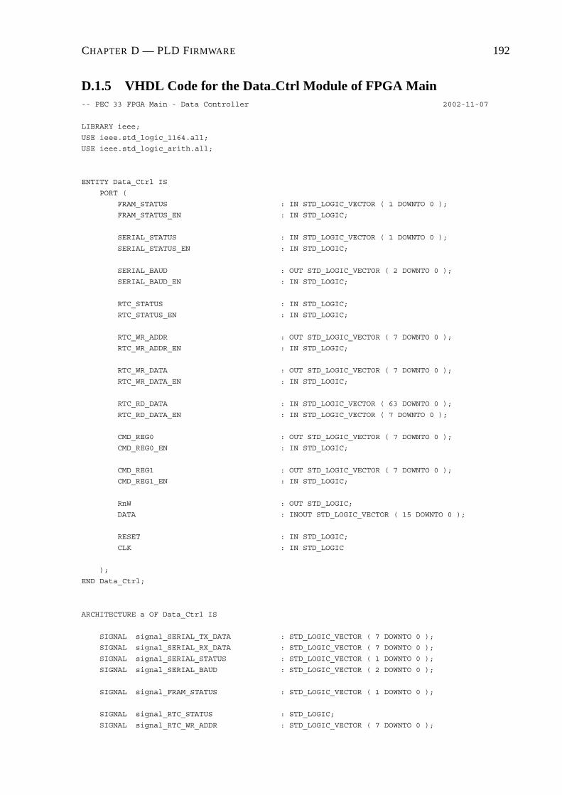
CHAPTER D — PLD FIRMWARE 192
D.1.5 VHDL Code for the Data Ctrl Module of FPGA Main-- PEC 33 FPGA Main - Data Controller 2002-11-07
LIBRARY ieee;
USE ieee.std_logic_1164.all;
USE ieee.std_logic_arith.all;
ENTITY Data_Ctrl IS
PORT (
FRAM_STATUS : IN STD_LOGIC_VECTOR ( 1 DOWNTO 0 );
FRAM_STATUS_EN : IN STD_LOGIC;
SERIAL_STATUS : IN STD_LOGIC_VECTOR ( 1 DOWNTO 0 );
SERIAL_STATUS_EN : IN STD_LOGIC;
SERIAL_BAUD : OUT STD_LOGIC_VECTOR ( 2 DOWNTO 0 );
SERIAL_BAUD_EN : IN STD_LOGIC;
RTC_STATUS : IN STD_LOGIC;
RTC_STATUS_EN : IN STD_LOGIC;
RTC_WR_ADDR : OUT STD_LOGIC_VECTOR ( 7 DOWNTO 0 );
RTC_WR_ADDR_EN : IN STD_LOGIC;
RTC_WR_DATA : OUT STD_LOGIC_VECTOR ( 7 DOWNTO 0 );
RTC_WR_DATA_EN : IN STD_LOGIC;
RTC_RD_DATA : IN STD_LOGIC_VECTOR ( 63 DOWNTO 0 );
RTC_RD_DATA_EN : IN STD_LOGIC_VECTOR ( 7 DOWNTO 0 );
CMD_REG0 : OUT STD_LOGIC_VECTOR ( 7 DOWNTO 0 );
CMD_REG0_EN : IN STD_LOGIC;
CMD_REG1 : OUT STD_LOGIC_VECTOR ( 7 DOWNTO 0 );
CMD_REG1_EN : IN STD_LOGIC;
RnW : OUT STD_LOGIC;
DATA : INOUT STD_LOGIC_VECTOR ( 15 DOWNTO 0 );
RESET : IN STD_LOGIC;
CLK : IN STD_LOGIC
);
END Data_Ctrl;
ARCHITECTURE a OF Data_Ctrl IS
SIGNAL signal_SERIAL_TX_DATA : STD_LOGIC_VECTOR ( 7 DOWNTO 0 );
SIGNAL signal_SERIAL_RX_DATA : STD_LOGIC_VECTOR ( 7 DOWNTO 0 );
SIGNAL signal_SERIAL_STATUS : STD_LOGIC_VECTOR ( 1 DOWNTO 0 );
SIGNAL signal_SERIAL_BAUD : STD_LOGIC_VECTOR ( 2 DOWNTO 0 );
SIGNAL signal_FRAM_STATUS : STD_LOGIC_VECTOR ( 1 DOWNTO 0 );
SIGNAL signal_RTC_STATUS : STD_LOGIC;
SIGNAL signal_RTC_WR_ADDR : STD_LOGIC_VECTOR ( 7 DOWNTO 0 );
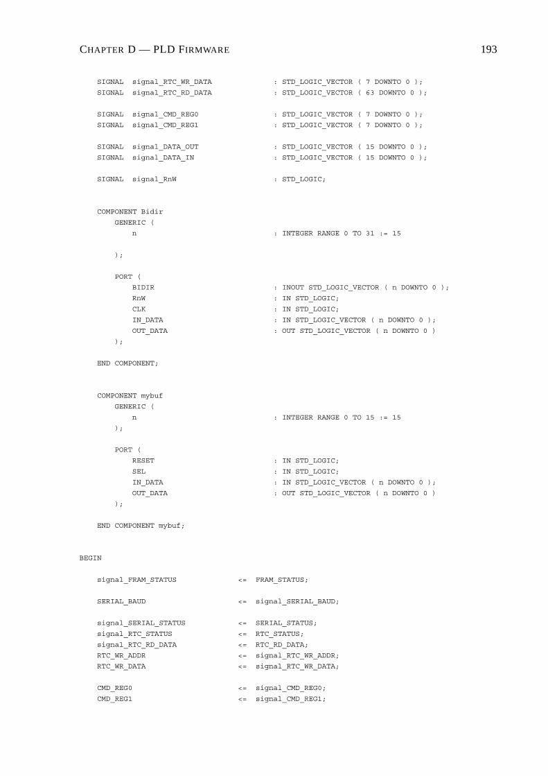
CHAPTER D — PLD FIRMWARE 193
SIGNAL signal_RTC_WR_DATA : STD_LOGIC_VECTOR ( 7 DOWNTO 0 );
SIGNAL signal_RTC_RD_DATA : STD_LOGIC_VECTOR ( 63 DOWNTO 0 );
SIGNAL signal_CMD_REG0 : STD_LOGIC_VECTOR ( 7 DOWNTO 0 );
SIGNAL signal_CMD_REG1 : STD_LOGIC_VECTOR ( 7 DOWNTO 0 );
SIGNAL signal_DATA_OUT : STD_LOGIC_VECTOR ( 15 DOWNTO 0 );
SIGNAL signal_DATA_IN : STD_LOGIC_VECTOR ( 15 DOWNTO 0 );
SIGNAL signal_RnW : STD_LOGIC;
COMPONENT Bidir
GENERIC (
n : INTEGER RANGE 0 TO 31 := 15
);
PORT (
BIDIR : INOUT STD_LOGIC_VECTOR ( n DOWNTO 0 );
RnW : IN STD_LOGIC;
CLK : IN STD_LOGIC;
IN_DATA : IN STD_LOGIC_VECTOR ( n DOWNTO 0 );
OUT_DATA : OUT STD_LOGIC_VECTOR ( n DOWNTO 0 )
);
END COMPONENT;
COMPONENT mybuf
GENERIC (
n : INTEGER RANGE 0 TO 15 := 15
);
PORT (
RESET : IN STD_LOGIC;
SEL : IN STD_LOGIC;
IN_DATA : IN STD_LOGIC_VECTOR ( n DOWNTO 0 );
OUT_DATA : OUT STD_LOGIC_VECTOR ( n DOWNTO 0 )
);
END COMPONENT mybuf;
BEGIN
signal_FRAM_STATUS <= FRAM_STATUS;
SERIAL_BAUD <= signal_SERIAL_BAUD;
signal_SERIAL_STATUS <= SERIAL_STATUS;
signal_RTC_STATUS <= RTC_STATUS;
signal_RTC_RD_DATA <= RTC_RD_DATA;
RTC_WR_ADDR <= signal_RTC_WR_ADDR;
RTC_WR_DATA <= signal_RTC_WR_DATA;
CMD_REG0 <= signal_CMD_REG0;
CMD_REG1 <= signal_CMD_REG1;

CHAPTER D — PLD FIRMWARE 194
------------------------------------------------------------------------------------------
serial_baud_map:
MyBuf GENERIC MAP ( n => 2 )
PORT MAP ( RESET => RESET, SEL => SERIAL_BAUD_EN,
IN_DATA => signal_DATA_IN ( 2 DOWNTO 0 ),
OUT_DATA => signal_SERIAL_BAUD );
------------------------------------------------------------------------------------------
rtc_wr_addr_map:
MyBuf GENERIC MAP ( n => 7 )
PORT MAP ( RESET => RESET, SEL => RTC_WR_ADDR_EN,
IN_DATA => signal_DATA_IN ( 7 DOWNTO 0 ),
OUT_DATA => signal_RTC_WR_ADDR );
rtc_wr_data_map:
MyBuf GENERIC MAP ( n => 7 )
PORT MAP ( RESET => RESET, SEL => RTC_WR_DATA_EN,
IN_DATA => signal_DATA_IN ( 7 DOWNTO 0 ),
OUT_DATA => signal_RTC_WR_DATA );
------------------------------------------------------------------------------------------
cmd_reg0_map:
MyBuf GENERIC MAP ( n => 7 )
PORT MAP ( RESET => RESET, SEL => CMD_REG0_EN,
IN_DATA => signal_DATA_IN ( 7 DOWNTO 0 ),
OUT_DATA => signal_CMD_REG0 );
cmd_reg1_map:
MyBuf GENERIC MAP ( n => 7 )
PORT MAP ( RESET => RESET, SEL => CMD_REG1_EN,
IN_DATA => signal_DATA_IN ( 7 DOWNTO 0 ),
OUT_DATA => signal_CMD_REG1 );
------------------------------------------------------------------------------------------
bidir_bus_map:
bidir GENERIC MAP ( n => 15 )
PORT MAP ( BIDIR => DATA, RnW => signal_RnW, CLK => CLK,
IN_DATA => signal_DATA_OUT,
OUT_DATA => signal_DATA_IN );
------------------------------------------------------------------------------------------
signal_RnW <= ’0’ WHEN ( SERIAL_STATUS_EN = ’1’ )or
( FRAM_STATUS_EN = ’1’ )or
( RTC_STATUS_EN = ’1’ )or
( RTC_RD_DATA_EN /= "00000000" ) ELSE
’1’;
RnW <= signal_RnW;
signal_DATA_OUT( 0 )
<= signal_SERIAL_STATUS ( 0 ) WHEN ( SERIAL_STATUS_EN = ’1’ ) ELSE
signal_FRAM_STATUS ( 0 ) WHEN ( FRAM_STATUS_EN = ’1’ ) ELSE
signal_RTC_STATUS WHEN ( RTC_STATUS_EN = ’1’ ) ELSE
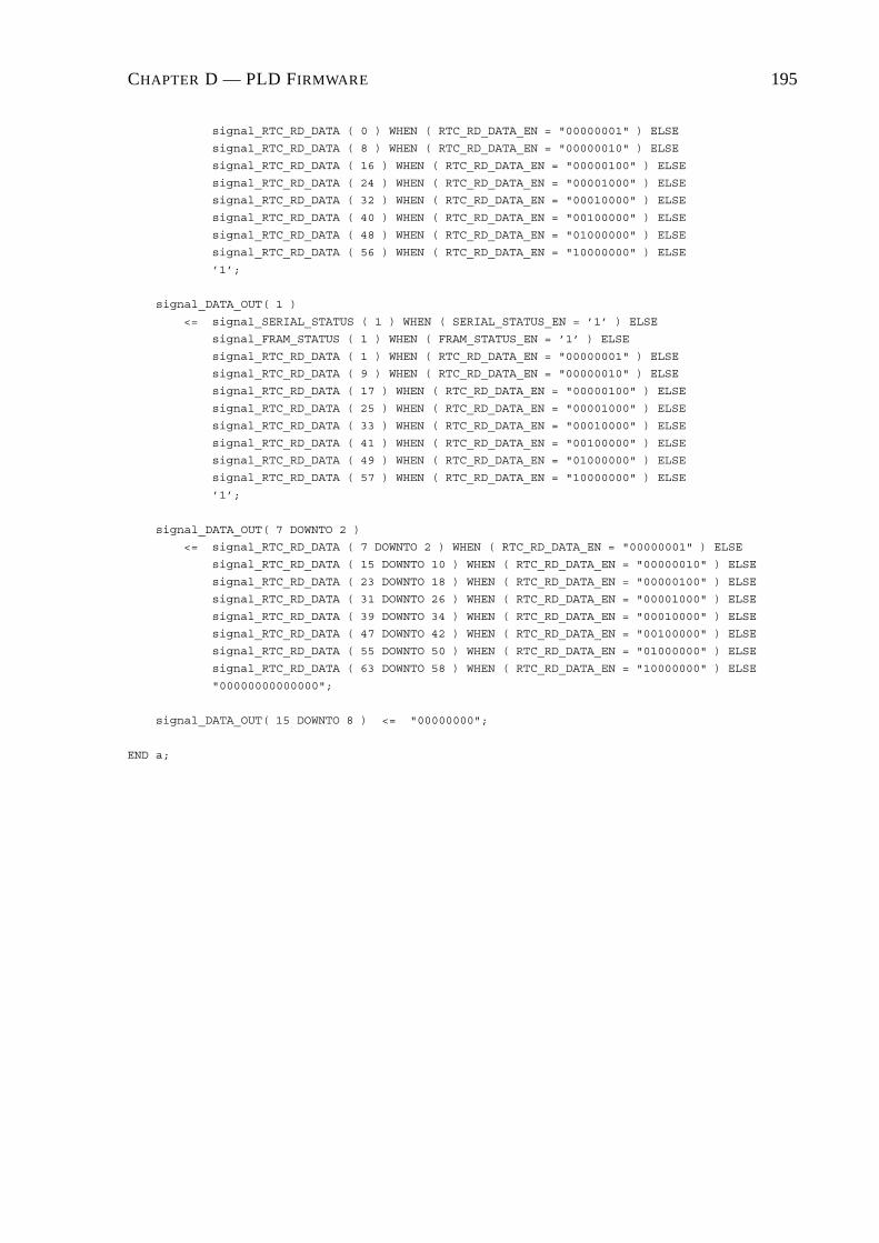
CHAPTER D — PLD FIRMWARE 195
signal_RTC_RD_DATA ( 0 ) WHEN ( RTC_RD_DATA_EN = "00000001" ) ELSE
signal_RTC_RD_DATA ( 8 ) WHEN ( RTC_RD_DATA_EN = "00000010" ) ELSE
signal_RTC_RD_DATA ( 16 ) WHEN ( RTC_RD_DATA_EN = "00000100" ) ELSE
signal_RTC_RD_DATA ( 24 ) WHEN ( RTC_RD_DATA_EN = "00001000" ) ELSE
signal_RTC_RD_DATA ( 32 ) WHEN ( RTC_RD_DATA_EN = "00010000" ) ELSE
signal_RTC_RD_DATA ( 40 ) WHEN ( RTC_RD_DATA_EN = "00100000" ) ELSE
signal_RTC_RD_DATA ( 48 ) WHEN ( RTC_RD_DATA_EN = "01000000" ) ELSE
signal_RTC_RD_DATA ( 56 ) WHEN ( RTC_RD_DATA_EN = "10000000" ) ELSE
’1’;
signal_DATA_OUT( 1 )
<= signal_SERIAL_STATUS ( 1 ) WHEN ( SERIAL_STATUS_EN = ’1’ ) ELSE
signal_FRAM_STATUS ( 1 ) WHEN ( FRAM_STATUS_EN = ’1’ ) ELSE
signal_RTC_RD_DATA ( 1 ) WHEN ( RTC_RD_DATA_EN = "00000001" ) ELSE
signal_RTC_RD_DATA ( 9 ) WHEN ( RTC_RD_DATA_EN = "00000010" ) ELSE
signal_RTC_RD_DATA ( 17 ) WHEN ( RTC_RD_DATA_EN = "00000100" ) ELSE
signal_RTC_RD_DATA ( 25 ) WHEN ( RTC_RD_DATA_EN = "00001000" ) ELSE
signal_RTC_RD_DATA ( 33 ) WHEN ( RTC_RD_DATA_EN = "00010000" ) ELSE
signal_RTC_RD_DATA ( 41 ) WHEN ( RTC_RD_DATA_EN = "00100000" ) ELSE
signal_RTC_RD_DATA ( 49 ) WHEN ( RTC_RD_DATA_EN = "01000000" ) ELSE
signal_RTC_RD_DATA ( 57 ) WHEN ( RTC_RD_DATA_EN = "10000000" ) ELSE
’1’;
signal_DATA_OUT( 7 DOWNTO 2 )
<= signal_RTC_RD_DATA ( 7 DOWNTO 2 ) WHEN ( RTC_RD_DATA_EN = "00000001" ) ELSE
signal_RTC_RD_DATA ( 15 DOWNTO 10 ) WHEN ( RTC_RD_DATA_EN = "00000010" ) ELSE
signal_RTC_RD_DATA ( 23 DOWNTO 18 ) WHEN ( RTC_RD_DATA_EN = "00000100" ) ELSE
signal_RTC_RD_DATA ( 31 DOWNTO 26 ) WHEN ( RTC_RD_DATA_EN = "00001000" ) ELSE
signal_RTC_RD_DATA ( 39 DOWNTO 34 ) WHEN ( RTC_RD_DATA_EN = "00010000" ) ELSE
signal_RTC_RD_DATA ( 47 DOWNTO 42 ) WHEN ( RTC_RD_DATA_EN = "00100000" ) ELSE
signal_RTC_RD_DATA ( 55 DOWNTO 50 ) WHEN ( RTC_RD_DATA_EN = "01000000" ) ELSE
signal_RTC_RD_DATA ( 63 DOWNTO 58 ) WHEN ( RTC_RD_DATA_EN = "10000000" ) ELSE
"00000000000000";
signal_DATA_OUT( 15 DOWNTO 8 ) <= "00000000";
END a;

CHAPTER D — PLD FIRMWARE 196
D.1.6 VHDL Code for the MyBuf Module of FPGA Main-- PEC33 - Buffer 2002-10-28
LIBRARY ieee;
USE ieee.std_logic_1164.all;
USE ieee.std_logic_arith.all;
-- -------------------------------------------------------
-- | RESET | SEL | IN_DATA | OUT_DATA |
-- -------------------------------------------------------
-- -------------------------------------------------------
-- | 1 | X | XX...X | 00...0 |
-- -------------------------------------------------------
-- | 0 | 1 | Data | IN_DATA |
-- -------------------------------------------------------
-- | 0 | 0 | XX...X | OUT_DATA |
-- -------------------------------------------------------
ENTITY mybuf IS
GENERIC (
n : INTEGER RANGE 0 TO 15 := 15
);
PORT (
RESET : IN STD_LOGIC;
SEL : IN STD_LOGIC;
IN_DATA : IN STD_LOGIC_VECTOR ( n DOWNTO 0 );
OUT_DATA : OUT STD_LOGIC_VECTOR ( n DOWNTO 0 )
);
END mybuf;
ARCHITECTURE a OF mybuf IS
SIGNAL signal_out : STD_LOGIC_VECTOR ( n DOWNTO 0 );
BEGIN
signal_out <= ( OTHERS => ’0’ ) WHEN ( RESET = ’1’ ) ELSE
IN_DATA WHEN ( SEL = ’1’ ) ELSE
signal_out;
OUT_DATA <= signal_out;
END a;

CHAPTER D — PLD FIRMWARE 197
D.1.7 VHDL Code for the BiDir Module of FPGA Main-- Bidirectional Bus 2002-11-07
LIBRARY ieee;
USE ieee.std_logic_1164.all;
USE ieee.std_logic_arith.all;
-- -------------------------------------------------------------------
-- | RnW | BIDIR | IN_DATA | OUT_DATA |
-- -------------------------------------------------------------------
-- -------------------------------------------------------------------
-- | 1 | ZZZZZZZZZZZZZZZZ | XXXXXXXXXXXXXXXX | BIDIR |
-- -------------------------------------------------------------------
-- | 0 | IN_DATA | Data | BIDIR |
-- -------------------------------------------------------------------
ENTITY Bidir IS
GENERIC (
n : INTEGER RANGE 0 TO 31 := 15
);
PORT (
BIDIR : INOUT STD_LOGIC_VECTOR ( n DOWNTO 0 );
RnW : IN STD_LOGIC;
CLK : IN STD_LOGIC;
IN_DATA : IN STD_LOGIC_VECTOR ( n DOWNTO 0 );
OUT_DATA : OUT STD_LOGIC_VECTOR ( n DOWNTO 0 )
);
END Bidir;
ARCHITECTURE maxpld OF Bidir IS
SIGNAL a : STD_LOGIC_VECTOR ( n DOWNTO 0 );
SIGNAL b : STD_LOGIC_VECTOR ( n DOWNTO 0 );
BEGIN
PROCESS ( CLK )
BEGIN
IF ( CLK’event )and( CLK = ’0’ ) THEN
a <= IN_DATA;
OUT_DATA <= b;
END IF;
END PROCESS;
PROCESS ( RnW, BIDIR )
BEGIN
IF ( RnW = ’1’ ) THEN
BIDIR <= ( others => ’Z’ );
b <= BIDIR;
ELSE
BIDIR <= a;
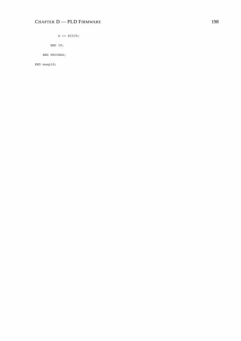
CHAPTER D — PLD FIRMWARE 198
b <= BIDIR;
END IF;
END PROCESS;
END maxpld;

CHAPTER D — PLD FIRMWARE 199
D.1.8 VHDL Code for the FRAM Ctrl Module of FPGA Main-- PEC33 Main - Flash RAM Controller 2002-11-07
LIBRARY ieee;
USE ieee.std_logic_1164.all;
USE ieee.std_logic_arith.all;
ENTITY FRAM_Ctrl IS
PORT (
FRAM_nCE : OUT STD_LOGIC;
FRAM_nOE : OUT STD_LOGIC;
FRAM_nWE : OUT STD_LOGIC;
FRAM_nRST : OUT STD_LOGIC;
DSP_nSTRB : IN STD_LOGIC;
DSP_RnW : IN STD_LOGIC;
nEN : IN STD_LOGIC;
RESET : IN STD_LOGIC;
CLK : IN STD_LOGIC --75MHZ DSP_H1
);
END FRAM_Ctrl;
ARCHITECTURE a OF FRAM_Ctrl IS
TYPE fram_statetype IS ( idle_state, wr_state_start, wr_state_end, rd_state );
SIGNAL state, next_state : fram_statetype;
SIGNAL state_cntr : INTEGER RANGE 0 TO 15;
SIGNAL signal_FRAM_nCE : STD_LOGIC;
SIGNAL signal_FRAM_nOE : STD_LOGIC;
SIGNAL signal_FRAM_nWE : STD_LOGIC;
BEGIN
FRAM_nRST <= ’1’;
FRAM_nCE <= signal_FRAM_nCE WHEN DSP_nSTRB = ’0’ ELSE ’1’;
FRAM_nOE <= signal_FRAM_nOE WHEN DSP_nSTRB = ’0’ ELSE ’1’;
FRAM_nWE <= signal_FRAM_nWE WHEN DSP_nSTRB = ’0’ ELSE ’1’;
------------------------------------------------------------------------------------------
fram_ctrl_proc:
PROCESS ( state )
BEGIN
IF ( state = idle_state ) THEN
signal_FRAM_nCE <= ’1’;
signal_FRAM_nOE <= ’1’;
signal_FRAM_nWE <= ’1’;
ELSIF ( state = wr_state_start ) THEN
signal_FRAM_nCE <= ’0’;
signal_FRAM_nOE <= ’1’;
signal_FRAM_nWE <= ’0’;
ELSIF ( state = wr_state_end ) THEN

CHAPTER D — PLD FIRMWARE 200
signal_FRAM_nCE <= ’0’;
signal_FRAM_nOE <= ’1’;
signal_FRAM_nWE <= ’1’;
ELSIF ( state = rd_state ) THEN
signal_FRAM_nCE <= ’0’;
signal_FRAM_nOE <= ’0’;
signal_FRAM_nWE <= ’1’;
END IF;
END PROCESS fram_ctrl_proc;
------------------------------------------------------------------------------------------
sm_proc:
PROCESS ( state )
BEGIN
CASE state IS
WHEN idle_state =>
next_state <= idle_state;
WHEN wr_state_start =>
next_state <= wr_state_end;
WHEN wr_state_end =>
next_state <= idle_state;
WHEN rd_state =>
next_state <= idle_state;
END CASE;
END PROCESS sm_proc;
------------------------------------------------------------------------------------------
sm_ctrl_proc:
PROCESS ( CLK, RESET )
BEGIN
IF ( RESET = ’1’ ) THEN
state <= idle_state;
ELSIF ( CLK’event )and( CLK = ’0’ ) THEN
IF ( nEN = ’0’ )and( DSP_nSTRB = ’0’ ) THEN
IF ( state = idle_state ) THEN
IF ( DSP_RnW = ’1’ ) THEN
state <= rd_state;
ELSE
state <= wr_state_start;

CHAPTER D — PLD FIRMWARE 201
END IF;
ELSIF ( state = wr_state_start ) THEN
IF ( state_cntr <= 2 ) THEN
state <= wr_state_start;
ELSE
state <= next_state;
END IF;
ELSIF ( state = wr_state_end ) THEN
IF ( state_cntr <= 5 ) THEN
state <= wr_state_end;
ELSE
state <= next_state;
END IF;
ELSIF ( state = rd_state ) THEN
IF ( state_cntr < 6 ) THEN
state <= rd_state;
ELSE
state <= next_state;
END IF;
END IF;
ELSE
state <= idle_state;
END IF;
END IF;
END PROCESS sm_ctrl_proc;
------------------------------------------------------------------------------------------
state_cntr_proc:
PROCESS ( CLK, RESET )
BEGIN
IF ( RESET = ’1’ ) THEN
state_cntr <= 0;
ELSIF ( CLK’event )and( CLK = ’1’ ) THEN
IF ( nEN = ’0’ )and( state /= idle_state ) THEN
state_cntr <= state_cntr+1;
ELSE
state_cntr <= 0;

CHAPTER D — PLD FIRMWARE 202
END IF;
END IF;
END PROCESS state_cntr_proc;
END a;

CHAPTER D — PLD FIRMWARE 203
D.1.9 VHDL Code for the RTC Ctrl Module of FPGA Main-- PEC33 Main - Real-Time Clock Controller 2002-11-07
LIBRARY ieee;
USE ieee.std_logic_1164.all;
USE ieee.std_logic_arith.all;
ENTITY RTC_Ctrl IS
PORT (
SDA : INOUT STD_LOGIC;
SCL : OUT STD_LOGIC;
RD_DATA : OUT STD_LOGIC_VECTOR ( 63 DOWNTO 0 );
WR_DATA : IN STD_LOGIC_VECTOR ( 7 DOWNTO 0 );
WR_nEN : IN STD_LOGIC;
RDYnBSY : OUT STD_LOGIC;
WR_ADDR : IN STD_LOGIC_VECTOR ( 7 DOWNTO 0 );
RESET : IN STD_LOGIC;
CLK : IN STD_LOGIC -- 30 MHz input clk
);
END RTC_Ctrl;
ARCHITECTURE a OF RTC_Ctrl IS
TYPE state_type IS ( idle_state, start_state, slave_addr_state, slave_addr_ack_state,
word_addr_state, word_addr_ack_state, tx_data_state,
tx_ack_state, tx_stop_state, rx_data_state, rx_ack_state,
rx_stop_state );
TYPE mode_type IS ( idle_mode, tx_mode, rx_mode, set_reg_pntr_mode );
TYPE mem_element IS ARRAY ( 0 TO 7 ) OF STD_LOGIC_VECTOR ( 7 DOWNTO 0 );
CONSTANT slave_rx_addr : STD_LOGIC_VECTOR := "11010000";
CONSTANT slave_tx_addr : STD_LOGIC_VECTOR := "11010001";
SIGNAL state : state_type;
SIGNAL next_state : state_type;
SIGNAL mode : mode_type;
SIGNAL slow_clk : STD_LOGIC;
SIGNAL sda_clk : STD_LOGIC;
SIGNAL state_clk : STD_LOGIC;
SIGNAL tx_start_trig : STD_LOGIC;
SIGNAL rx_start_trig : STD_LOGIC;
SIGNAL slave_ack_rec : STD_LOGIC;
SIGNAL word_addr_ack_rec : STD_LOGIC;
SIGNAL rx_ack_rec : STD_LOGIC;
SIGNAL memory : mem_element;
SIGNAL signal_addr : INTEGER RANGE 0 TO 7;
SIGNAL max_state_clk_cntr : INTEGER RANGE 0 TO 7;
SIGNAL bit_cntr : INTEGER RANGE 0 TO 7;
SIGNAL byte_cntr : INTEGER RANGE 0 TO 7;
SIGNAL tx_data : STD_LOGIC_VECTOR ( 7 DOWNTO 0 );
SIGNAL rx_data : STD_LOGIC_VECTOR ( 7 DOWNTO 0 );

CHAPTER D — PLD FIRMWARE 204
SIGNAL signal_SCL : STD_LOGIC;
SIGNAL signal_SDA : STD_LOGIC;
SIGNAL state_clk_cntr : INTEGER RANGE 0 TO 7;
SIGNAL signal_wr_addr : STD_LOGIC_VECTOR ( 7 DOWNTO 0 );
BEGIN
SCL <= signal_SCL;
------------------------------------------------------------------------------------------
wr_addr_proc:
PROCESS ( CLK, RESET )
BEGIN
IF ( RESET = ’1’ ) THEN
signal_wr_addr <= "00000000";
ELSIF ( CLK’event )and( CLK = ’1’ ) THEN
IF ( mode = idle_mode ) THEN
signal_wr_addr <= WR_ADDR;
ELSE
signal_wr_addr <= signal_wr_addr;
END IF;
END IF;
END PROCESS wr_addr_proc;
------------------------------------------------------------------------------------------
rd_data_proc:
PROCESS ( CLK, RESET )
BEGIN
IF ( RESET = ’1’ ) THEN
RD_DATA ( 7 DOWNTO 0 ) <= "00000000";
RD_DATA (15 DOWNTO 8 ) <= "00000000";
RD_DATA (23 DOWNTO 16) <= "00000000";
RD_DATA (31 DOWNTO 24) <= "00000000";
RD_DATA (39 DOWNTO 32) <= "00000000";
RD_DATA (47 DOWNTO 40) <= "00000000";
RD_DATA (55 DOWNTO 48) <= "00000000";
RD_DATA (63 DOWNTO 56) <= "00000000";
ELSIF ( CLK’event )and( CLK = ’1’ ) THEN
IF ( mode = idle_mode ) THEN
RD_DATA ( 7 DOWNTO 0 ) <= memory( 0 );
RD_DATA (15 DOWNTO 8 ) <= memory( 1 );
RD_DATA (23 DOWNTO 16) <= memory( 2 );
RD_DATA (31 DOWNTO 24) <= memory( 3 );
RD_DATA (39 DOWNTO 32) <= memory( 4 );
RD_DATA (47 DOWNTO 40) <= memory( 5 );
RD_DATA (55 DOWNTO 48) <= memory( 6 );
RD_DATA (63 DOWNTO 56) <= memory( 7 );
END IF;

CHAPTER D — PLD FIRMWARE 205
END IF;
END PROCESS rd_data_proc;
------------------------------------------------------------------------------------------
rdynbsy_proc:
PROCESS ( CLK, RESET )
BEGIN
IF ( RESET = ’1’ ) THEN
RDYnBSY <= ’1’;
ELSIF ( CLK’event )and( CLK = ’1’ ) THEN
IF ( mode = idle_mode ) THEN
RDYnBSY <= ’1’;
ELSE
RDYnBSY <= ’0’;
END IF;
END IF;
END PROCESS rdynbsy_proc;
------------------------------------------------------------------------------------------
scl_proc:
PROCESS ( CLK, RESET, state )
BEGIN
IF ( RESET = ’1’ )or( state = idle_state ) THEN
signal_SCL <= ’1’;
ELSIF ( CLK’event )and( CLK = ’1’ ) THEN
IF ( state /= idle_state )and( state /= start_state ) THEN
signal_SCL <= slow_clk;
ELSE
signal_SCL <= ’1’;
END IF;
END IF;
END PROCESS scl_proc;
------------------------------------------------------------------------------------------
state_clk_proc:
PROCESS ( CLK, RESET, state )
BEGIN
IF ( RESET = ’1’ )or( state = idle_state ) THEN
state_clk <= ’1’;
ELSIF ( CLK’event )and( CLK = ’1’ ) THEN
IF ( state /= idle_state )and( state /= start_state )and
( state /= rx_stop_state )and( state /= tx_stop_state ) THEN
state_clk <= sda_clk;
CHAPTER D — PLD FIRMWARE 206
ELSE
state_clk <= ’1’;
END IF;
END IF;
END PROCESS state_clk_proc;
------------------------------------------------------------------------------------------
memory_proc:
PROCESS ( CLK, RESET )
BEGIN
IF ( RESET = ’1’ ) THEN
memory( 0 ) <= "00000000";
memory( 1 ) <= "00000000";
memory( 2 ) <= "00000000";
memory( 3 ) <= "00000000";
memory( 4 ) <= "00000000";
memory( 5 ) <= "00000000";
memory( 6 ) <= "00000000";
memory( 7 ) <= "00000000";
ELSIF ( CLK’event )and( CLK = ’1’ ) THEN
IF ( state = rx_ack_state ) THEN
memory ( byte_cntr ) <= rx_data;
ELSE
memory <= memory;
END IF;
END IF;
END PROCESS memory_proc;
------------------------------------------------------------------------------------------
slave_ack_proc:
PROCESS ( signal_scl, RESET, state )
BEGIN
IF ( RESET = ’1’ )or( state = idle_state ) THEN
slave_ack_rec <= ’0’;
ELSIF ( signal_scl’event )and( signal_scl = ’1’ ) THEN
IF ( state = slave_addr_ack_state ) THEN
slave_ack_rec <= not SDA;
ELSE
slave_ack_rec <= ’0’;
END IF;
END IF;
END PROCESS slave_ack_proc;
------------------------------------------------------------------------------------------

CHAPTER D — PLD FIRMWARE 207
word_addr_ack_proc:
PROCESS ( signal_scl, RESET, state )
BEGIN
IF ( RESET = ’1’ )or( state = idle_state ) THEN
word_addr_ack_rec <= ’0’;
ELSIF ( signal_scl’event )and( signal_scl = ’1’ ) THEN
IF ( state = word_addr_ack_state ) THEN
word_addr_ack_rec <= not SDA;
ELSE
word_addr_ack_rec <= ’0’;
END IF;
END IF;
END PROCESS word_addr_ack_proc;
------------------------------------------------------------------------------------------
rx_data_proc:
PROCESS ( sda_clk, RESET )
VARIABLE temp : INTEGER RANGE 0 TO 7;
BEGIN
temp := 7 - state_clk_cntr;
IF ( RESET = ’1’ )or( state = idle_state ) THEN
rx_data <= "00000000";
ELSIF ( sda_clk’event )and( sda_clk = ’1’ ) THEN
IF ( state = rx_data_state ) THEN
rx_data ( temp ) <= SDA;
END IF;
END IF;
END PROCESS rx_data_proc;
------------------------------------------------------------------------------------------
tx_data_proc:
PROCESS ( CLK, RESET, state )
BEGIN
IF ( RESET = ’1’ )or( state = tx_stop_state ) THEN
tx_data <= "00000000";
ELSIF ( CLK’event )and( CLK = ’1’ ) THEN
IF ( mode /= tx_mode ) THEN
tx_data <= WR_DATA;
ELSE
tx_data <= tx_data;
END IF;
END IF;
CHAPTER D — PLD FIRMWARE 208
END PROCESS tx_data_proc;
------------------------------------------------------------------------------------------
sda_proc:
PROCESS ( sda_clk, RESET )
VARIABLE temp : STD_LOGIC;
BEGIN
IF ( state = idle_state )or( state = slave_addr_ack_state )or
( state = word_addr_ack_state )or( state = tx_ack_state )or
( temp = ’1’ ) THEN
SDA <= ’Z’;
ELSE
SDA <= signal_SDA;
END IF;
IF ( RESET = ’1’ ) THEN
signal_SDA <= ’1’;
temp := ’0’;
ELSIF ( sda_clk’event )and( sda_clk = ’0’ ) THEN
IF ( state = idle_state ) THEN
signal_SDA <= ’1’;
temp := ’0’;
ELSIF ( state = start_state ) THEN
signal_SDA <= ’0’;
temp := ’0’;
ELSIF ( state = slave_addr_state )and( mode = rx_mode ) THEN
signal_SDA <= slave_tx_addr( bit_cntr );
temp := ’0’;
ELSIF ( state = slave_addr_state ) THEN
signal_SDA <= slave_rx_addr( bit_cntr );
temp := ’0’;
ELSIF ( state = slave_addr_ack_state ) THEN
signal_SDA <= ’0’;
temp := ’0’;
ELSIF ( state = word_addr_state ) THEN
IF ( mode = tx_mode ) THEN
signal_SDA <= signal_wr_addr( bit_cntr );
ELSE
signal_SDA <= ’0’;
END IF;
temp := ’0’;
ELSIF ( state = word_addr_ack_state ) THEN
signal_SDA <= ’0’;
temp := ’0’;
ELSIF ( state = tx_ack_state ) THEN

CHAPTER D — PLD FIRMWARE 209
signal_SDA <= ’0’;
temp := ’0’;
ELSIF ( state = tx_data_state ) THEN
signal_SDA <= tx_data ( bit_cntr );
temp := ’0’;
ELSIF ( state = tx_stop_state ) THEN
IF ( mode = tx_mode ) THEN
signal_SDA <= ’0’;
ELSE
signal_SDA <= ’1’;
END IF;
temp := ’0’;
ELSIF ( state = rx_data_state ) THEN
signal_SDA <= ’0’;
temp := ’1’;
ELSIF ( state = rx_ack_state )and( byte_cntr < 7 ) THEN
signal_SDA <= ’0’;
temp := ’0’;
ELSIF ( state = rx_ack_state )and( byte_cntr = 7 ) THEN
signal_SDA <= ’1’;
temp := ’0’;
ELSIF ( state = rx_stop_state ) THEN
signal_SDA <= ’0’;
temp := ’0’;
ELSE
signal_SDA <= ’1’;
temp := temp;
END IF;
END IF;
END PROCESS sda_proc;
------------------------------------------------------------------------------------------
bit_cntr_proc:
PROCESS ( sda_clk, RESET, state )
BEGIN
IF ( RESET = ’1’ )or( state = idle_state )or( state = slave_addr_ack_state )or
( state = tx_ack_state )or
( state = rx_ack_state ) THEN
bit_cntr <= 7;
ELSIF ( sda_clk’event )and( sda_clk = ’0’ ) THEN
IF ( state = slave_addr_state )or( state = word_addr_state )or
( state = tx_data_state )or( state = rx_data_state ) THEN
bit_cntr <= bit_cntr-1;
END IF;

CHAPTER D — PLD FIRMWARE 210
END IF;
END PROCESS bit_cntr_proc;
------------------------------------------------------------------------------------------
byte_cntr_proc:
PROCESS ( state_clk, RESET, state )
BEGIN
IF ( RESET = ’1’ )or( state = idle_state )or( state = slave_addr_ack_state )or
( state = word_addr_ack_state ) THEN
byte_cntr <= 7;
ELSIF ( state_clk’event )and( state_clk = ’0’ ) THEN
IF ( ( state = tx_data_state )or( state = rx_data_state ) )and
( bit_cntr = 0 ) THEN
byte_cntr <= byte_cntr+1;
END IF;
END IF;
END PROCESS byte_cntr_proc;
------------------------------------------------------------------------------------------
sm_proc:
PROCESS ( state )
BEGIN
CASE state IS
WHEN idle_state =>
max_state_clk_cntr <= 0;
next_state <= start_state;
WHEN start_state =>
max_state_clk_cntr <= 0;
next_state <= slave_addr_state;
WHEN slave_addr_state =>
max_state_clk_cntr <= 7;
next_state <= slave_addr_ack_state;
WHEN slave_addr_ack_state =>
max_state_clk_cntr <= 0;
IF ( slave_ack_rec = ’1’ )and
( ( mode = tx_mode )or( mode = set_reg_pntr_mode ) ) THEN
next_state <= word_addr_state;
ELSIF ( slave_ack_rec = ’1’ )and( mode = rx_mode ) THEN
next_state <= rx_data_state;
ELSE
next_state <= slave_addr_state;
END IF;
WHEN word_addr_state =>

CHAPTER D — PLD FIRMWARE 211
max_state_clk_cntr <= 7;
next_state <= word_addr_ack_state;
WHEN word_addr_ack_state =>
max_state_clk_cntr <= 0;
IF ( mode = tx_mode ) THEN
next_state <= tx_data_state;
ELSIF ( mode = set_reg_pntr_mode ) THEN
next_state <= tx_stop_state;
ELSE
next_state <= word_addr_state;
END IF;
WHEN tx_data_state =>
max_state_clk_cntr <= 7;
next_state <= tx_ack_state;
WHEN tx_ack_state =>
max_state_clk_cntr <= 0;
next_state <= tx_stop_state;
WHEN tx_stop_state =>
max_state_clk_cntr <= 0;
IF ( mode = tx_mode ) THEN
next_state <= idle_state;
ELSE
next_state <= start_state;
END IF;
WHEN rx_data_state =>
max_state_clk_cntr <= 7;
next_state <= rx_ack_state;
WHEN rx_ack_state =>
max_state_clk_cntr <= 0;
IF ( byte_cntr = 7 ) THEN
next_state <= rx_stop_state;
ELSE
next_state <= rx_data_state;
END IF;
WHEN rx_stop_state =>
max_state_clk_cntr <= 0;
next_state <= idle_state;
WHEN others =>
max_state_clk_cntr <= max_state_clk_cntr;
next_state <= next_state;

CHAPTER D — PLD FIRMWARE 212
END CASE;
END PROCESS sm_proc;
------------------------------------------------------------------------------------------
sm_ctrl_proc:
PROCESS ( slow_clk, RESET )
BEGIN
IF ( RESET = ’1’ ) THEN
state <= idle_state;
state_clk_cntr <= 0;
ELSIF ( slow_clk’event )and( slow_clk = ’0’ ) THEN
IF ( ( ( tx_start_trig = ’1’ )or( rx_start_trig = ’1’ ) )and
( state = idle_state ) ) THEN
state <= start_state;
state_clk_cntr <= 0;
ELSIF ( state_clk_cntr = max_state_clk_cntr )and( state /= idle_state ) THEN
state <= next_state;
state_clk_cntr <= 0;
ELSIF ( state_clk_cntr /= max_state_clk_cntr )and( state /= idle_state ) THEN
state <= state;
state_clk_cntr <= state_clk_cntr + 1;
ELSE
state <= state;
state_clk_cntr <= state_clk_cntr;
END IF;
END IF;
END PROCESS sm_ctrl_proc;
------------------------------------------------------------------------------------------
tx_start_trig_proc:
PROCESS ( WR_nEN, RESET, state )
BEGIN
IF ( RESET = ’1’ )or( ( state = tx_stop_state )and( mode = tx_mode ) ) THEN
tx_start_trig <= ’0’;
ELSIF ( WR_nEN’event )and( WR_nEN = ’1’ ) THEN
tx_start_trig <= ’1’;
END IF;
END PROCESS tx_start_trig_proc;
------------------------------------------------------------------------------------------
rx_start_proc:
PROCESS ( CLK, RESET, state )
VARIABLE update_cntr : INTEGER RANGE 0 TO 30000000;

CHAPTER D — PLD FIRMWARE 213
BEGIN
IF ( RESET = ’1’ )or( state /= idle_state ) THEN
update_cntr := 0;
rx_start_trig <= ’0’;
ELSIF ( CLK’event )and( CLK = ’1’ ) THEN
IF ( update_cntr /= 3000000 ) THEN
update_cntr := update_cntr+1;
rx_start_trig <= ’0’;
ELSIF ( update_cntr = 3000000 )and( state = idle_state )and
( mode = idle_mode ) THEN
update_cntr := update_cntr;
rx_start_trig <= ’1’;
ELSE
update_cntr := update_cntr;
rx_start_trig <= rx_start_trig;
END IF;
END IF;
END PROCESS rx_start_proc;
------------------------------------------------------------------------------------------
mode_proc:
PROCESS ( CLK, RESET, state )
BEGIN
IF ( RESET = ’1’ ) THEN
mode <= idle_mode;
ELSIF ( CLK’event )and( CLK = ’1’ ) THEN
IF ( ( tx_start_trig = ’1’ )and( state = idle_state ) ) THEN
mode <= tx_mode;
ELSIF ( ( rx_start_trig = ’1’ )and( state = idle_state ) ) THEN
mode <= set_reg_pntr_mode;
ELSIF ( mode = set_reg_pntr_mode )and( state = tx_stop_state ) THEN
mode <= rx_mode;
ELSIF ( state = idle_state ) THEN
mode <= idle_mode;
ELSE
mode <= mode;
END IF;
END IF;
END PROCESS mode_proc;
------------------------------------------------------------------------------------------
sda_clk_proc:
CHAPTER D — PLD FIRMWARE 214
PROCESS ( CLK, RESET )
VARIABLE sda_clk_cntr : INTEGER RANGE 0 TO 150;
BEGIN
IF ( RESET = ’1’ ) THEN
sda_clk_cntr := 75;
sda_clk <= ’0’;
ELSIF ( CLK’event )and( CLK = ’1’ ) THEN
IF ( sda_clk_cntr < 150 ) THEN
sda_clk <= sda_clk;
sda_clk_cntr := sda_clk_cntr + 1;
ELSE
sda_clk <= not sda_clk;
sda_clk_cntr := 0;
END IF;
END IF;
END PROCESS sda_clk_proc;
------------------------------------------------------------------------------------------
slow_clk_proc:
PROCESS ( CLK, RESET )
VARIABLE slow_clk_cntr : INTEGER RANGE 0 TO 150;
BEGIN
IF ( RESET = ’1’ ) THEN
slow_clk_cntr := 0;
slow_clk <= ’1’;
ELSIF ( CLK’event )and( CLK = ’1’ ) THEN
IF ( slow_clk_cntr < 150 ) THEN
slow_clk <= slow_clk;
slow_clk_cntr := slow_clk_cntr + 1;
ELSE
slow_clk <= not slow_clk;
slow_clk_cntr := 0;
END IF;
END IF;
END PROCESS slow_clk_proc;
END a;

CHAPTER D — PLD FIRMWARE 215
D.1.10 Graphical Design File for the SP Ctrl Module of FPGA Main
GLOBAL_RESETGLOBAL_CLK
SP_BAUDRATE[2..0]SP_DATA_SENT
SP_TX_DATA_RDYSP_TX_DATA[7..0]
TX_RDY
SP_RX_DATA[7..0]SP_DATA_REC
GLOBAL_RESET
SP_TX_DATA_RDYSP_TX_DATA[7..0]
SP_TX_RDYnBSY
TX_RDYSP_DATA_SENT
GLOBAL_CLKGLOBAL_RESETSP_DATA_RECSP_RX_DATA[7..0]
SP_BAUDRATE[2..0]INPUT
GLOBAL_RESETINPUT
GLOBAL_CLKINPUT
SP_RX INPUT
SP_TXOUTPUT
DSP_H1 INPUT
DSP_CLKX0INPUT
DSP_FSX0INPUT
DSP_DX0 INPUT
SP_TX_RDYnBSYOUTPUT
DSP_CLKR0OUTPUTDSP_FSR0OUTPUTDSP_DR0OUTPUT
Figure D.4: Graphical Design File of the SP Ctrl Symbol

CHAPTER D — PLD FIRMWARE 216
D.1.11 VHDL Code for the UART Ctrl Module of FPGA Main-- PEC33 Main - UART Controller 2002-11-07
LIBRARY ieee;
USE ieee.std_logic_1164.all;
USE ieee.std_logic_arith.all;
-- Word Length: 8
-- Parity: Even
-- -------------------------------------------
-- | Baudrate | Baudrate | CLK Constant |
-- | | Input | for 30 MHz |
-- -------------------------------------------
-- -------------------------------------------
-- | 1200 | 001 | 1562 |
-- | 2400 | 010 | 781 |
-- | 9600 |000 or 011 | 195 |
-- | 19200 | 100 | 98 |
-- -------------------------------------------
ENTITY UART_Ctrl IS
PORT (
RX_DATA_IN : IN STD_LOGIC;
RX_DATA_OUT : OUT STD_LOGIC_VECTOR( 7 DOWNTO 0 );
DATA_REC : OUT STD_LOGIC;
TX_DATA_IN : IN STD_LOGIC_VECTOR( 7 DOWNTO 0 );
TX_DATA_OUT : OUT STD_LOGIC;
TX_DATA_RDY : IN STD_LOGIC;
TX_RDY : OUT STD_LOGIC;
DATA_SENT : OUT STD_LOGIC;
BAUDRATE : IN STD_LOGIC_VECTOR( 2 DOWNTO 0 );
RESET : IN STD_LOGIC;
CLK : IN STD_LOGIC -- 30 kHz input clk
);
END UART_Ctrl;
ARCHITECTURE a OF UART_Ctrl IS
TYPE rx_state_type IS ( idle_state, start_state, sampling_state, parity_state,
stop_state );
TYPE tx_state_type IS ( idle_state, start_state, tx_data_state, parity_state,
stop_state );
-- oversampling clk - Freq = 16 x baudrate
SIGNAL baud_clk : STD_LOGIC;
-- Counter dividing CLK to get baud_clk
SIGNAL max_baud_cntr : INTEGER RANGE 0 TO 8191;
SIGNAL halfmax_baud_cntr : INTEGER RANGE 0 TO 8191;
SIGNAL error_reg : STD_LOGIC_VECTOR ( 1 DOWNTO 0 );

CHAPTER D — PLD FIRMWARE 217
SIGNAL rx_state : rx_state_type;
SIGNAL next_rx_state : rx_state_type;
SIGNAL rx_bit_cntr : INTEGER RANGE 0 TO 8;
-- RX oversampling counter
SIGNAL rx_os_cntr : INTEGER RANGE 0 TO 15;
SIGNAL rx_os_cntr_trigval : INTEGER RANGE 0 TO 15;
SIGNAL rx_sample_data : STD_LOGIC_VECTOR ( 8 DOWNTO 0 );
SIGNAL rx_parity : STD_LOGIC;
SIGNAL rx_parity_chk : STD_LOGIC;
SIGNAL stopbit : STD_LOGIC;
SIGNAL rx_start_trig : STD_LOGIC;
SIGNAL tx_state : tx_state_type;
SIGNAL next_tx_state : tx_state_type;
SIGNAL tx_bit_cntr : INTEGER RANGE 0 TO 8;
-- TX oversampling counter
SIGNAL tx_os_cntr : INTEGER RANGE 0 TO 15;
SIGNAL tx_sample_data : STD_LOGIC_VECTOR ( 8 DOWNTO 0 );
SIGNAL tx_parity : STD_LOGIC;
SIGNAL tx_start_trig : STD_LOGIC;
SIGNAL new_tx_data : STD_LOGIC_VECTOR ( 7 DOWNTO 0 );
SIGNAL new_rx_data : STD_LOGIC_VECTOR ( 7 DOWNTO 0 );
SIGNAL rx_sent : STD_LOGIC;
SIGNAL baud_cntr : INTEGER RANGE 0 TO 8191;
BEGIN
TX_RDY <= ’1’ WHEN ( tx_state = idle_state ) ELSE
’0’;
RX_DATA_OUT <= new_rx_data;
DATA_SENT <= ’0’ WHEN ( RESET = ’1’ ) ELSE
’1’ WHEN ( tx_state = stop_state ) ELSE
’0’ WHEN ( tx_state = start_state )or
( tx_state = tx_data_state );
max_baud_cntr <= 195 WHEN ( BAUDRATE = "000" ) ELSE
1562 WHEN ( BAUDRATE = "001" ) ELSE
781 WHEN ( BAUDRATE = "010" ) ELSE
195 WHEN ( BAUDRATE = "011" ) ELSE
98 WHEN ( BAUDRATE = "100" ) ELSE
781;
halfmax_baud_cntr <= 97 WHEN ( BAUDRATE = "000" ) ELSE
781 WHEN ( BAUDRATE = "001" ) ELSE
390 WHEN ( BAUDRATE = "010" ) ELSE
97 WHEN ( BAUDRATE = "011" ) ELSE
49 WHEN ( BAUDRATE = "100" ) ELSE
390;
------------------------------------------------------------------------------------------
baudrate_proc:

CHAPTER D — PLD FIRMWARE 218
PROCESS ( CLK, RESET )
BEGIN
IF ( RESET = ’1’ ) THEN
baud_cntr <= 1;
baud_clk <= ’1’;
ELSIF ( CLK’event )and( CLK = ’1’ ) THEN
IF ( baud_cntr < halfmax_baud_cntr ) THEN
baud_clk <= ’1’;
baud_cntr <= baud_cntr + 1;
ELSIF ( baud_cntr < max_baud_cntr ) THEN
baud_clk <= ’0’;
baud_cntr <= baud_cntr + 1;
ELSE
baud_clk <= ’1’;
baud_cntr <= 1;
END IF;
END IF;
END PROCESS baudrate_proc;
------------------------------------------------------------------------------------------
data_rec_proc:
PROCESS ( CLK, RESET, rx_state )
BEGIN
IF ( RESET = ’1’ )or( rx_state /= parity_state ) THEN
DATA_REC <= ’0’;
rx_sent <= ’0’;
ELSIF ( CLK’event )and( CLK = ’1’ ) THEN
IF ( rx_state = parity_state )and( rx_sent = ’0’ ) THEN
DATA_REC <= ’1’;
rx_sent <= ’1’;
ELSE
DATA_REC <= ’0’;
rx_sent <= ’1’;
END IF;
END IF;
END PROCESS data_rec_proc;
------------------------------------------------------------------------------------------
rx_os_cntr_proc:
PROCESS ( baud_clk, RESET )
BEGIN
IF ( RESET = ’1’ ) THEN
rx_os_cntr <= 0;

CHAPTER D — PLD FIRMWARE 219
ELSIF ( baud_clk’event )and( baud_clk = ’1’ ) THEN
IF ( rx_state /= idle_state)and( rx_os_cntr < 15 ) THEN
rx_os_cntr <= rx_os_cntr + 1;
ELSIF ( rx_state /= idle_state)and( rx_os_cntr = 15 ) THEN
rx_os_cntr <= 0;
END IF;
END IF;
END PROCESS rx_os_cntr_proc;
------------------------------------------------------------------------------------------
bit_cntr_proc:
PROCESS ( baud_clk, RESET )
BEGIN
IF ( RESET = ’1’ ) THEN
rx_bit_cntr <= 0;
rx_parity_chk <= ’0’;
ELSIF ( baud_clk’event )and( baud_clk = ’1’ ) THEN
IF ( rx_state = start_state ) THEN
rx_bit_cntr <= 0;
rx_parity_chk <= ’0’;
ELSIF ( rx_state = sampling_state)and
( rx_os_cntr = rx_os_cntr_trigval ) THEN
rx_bit_cntr <= rx_bit_cntr + 1;
IF ( RX_DATA_IN = ’1’ ) THEN
rx_parity_chk <= not rx_parity_chk;
END IF;
ELSIF ( rx_state = parity_state)and
( rx_os_cntr = rx_os_cntr_trigval ) THEN
rx_bit_cntr <= 0;
rx_parity_chk <= rx_parity_chk;
ELSIF ( rx_state = stop_state)and
( rx_os_cntr = rx_os_cntr_trigval ) THEN
rx_bit_cntr <= 0;
rx_parity_chk <= rx_parity_chk;
ELSIF ( rx_state = idle_state ) THEN
rx_bit_cntr <= 0;
rx_parity_chk <= ’0’;
ELSE
rx_bit_cntr <= rx_bit_cntr;
rx_parity_chk <= rx_parity_chk;
END IF;
END IF;

CHAPTER D — PLD FIRMWARE 220
END PROCESS bit_cntr_proc;
------------------------------------------------------------------------------------------
sample_bit_proc:
PROCESS ( CLK, RESET )
BEGIN
IF ( RESET = ’1’ ) THEN
rx_sample_data <= "000000000";
rx_parity <= ’0’;
stopbit <= ’0’;
error_reg <= "00";
ELSIF ( CLK’event )and( CLK = ’1’ ) THEN
IF ( rx_state = start_state ) THEN
rx_sample_data <= "000000000";
rx_parity <= ’0’;
stopbit <= ’0’;
error_reg <= "00";
ELSIF ( rx_state = sampling_state)and
( rx_os_cntr = rx_os_cntr_trigval ) THEN
rx_sample_data( rx_bit_cntr ) <= RX_DATA_IN;
rx_parity <= ’0’;
stopbit <= ’0’;
error_reg <= error_reg;
ELSIF ( rx_state = parity_state)and
( rx_os_cntr = rx_os_cntr_trigval ) THEN
rx_sample_data <= rx_sample_data;
rx_parity <= RX_DATA_IN;
stopbit <= ’0’;
error_reg(0) <= error_reg(0);
error_reg(1) <= error_reg(1);
ELSIF ( rx_state = stop_state)and
( rx_os_cntr = rx_os_cntr_trigval ) THEN
rx_sample_data <= rx_sample_data;
rx_parity <= rx_parity;
stopbit <= RX_DATA_IN;
error_reg(1) <= error_reg(1);
error_reg(0) <= ( rx_parity )xor( rx_parity_chk );
ELSIF ( rx_state = idle_state ) THEN
rx_sample_data <= rx_sample_data;
rx_parity <= rx_parity;
stopbit <= stopbit;
error_reg(1) <= not( stopbit );
error_reg(0) <= error_reg(0);
ELSE
rx_sample_data <= rx_sample_data;
rx_parity <= rx_parity;
stopbit <= stopbit;
error_reg <= error_reg;

CHAPTER D — PLD FIRMWARE 221
END IF;
END IF;
END PROCESS sample_bit_proc;
------------------------------------------------------------------------------------------
rx_sm_proc:
PROCESS ( rx_state )
BEGIN
CASE rx_state IS
WHEN idle_state =>
rx_os_cntr_trigval <= 0;
next_rx_state <= start_state;
WHEN start_state =>
rx_os_cntr_trigval <= 1;
next_rx_state <= sampling_state;
WHEN sampling_state =>
rx_os_cntr_trigval <= 6;
IF ( rx_bit_cntr < 8 ) THEN
next_rx_state <= sampling_state;
ELSE
next_rx_state <= parity_state;
END IF;
WHEN parity_state =>
rx_os_cntr_trigval <= 6;
next_rx_state <= stop_state;
WHEN stop_state =>
rx_os_cntr_trigval <= 6;
next_rx_state <= idle_state;
END CASE;
END PROCESS rx_sm_proc;
------------------------------------------------------------------------------------------
rx_data_proc:
PROCESS ( CLK, RESET, rx_state )
BEGIN
IF ( RESET = ’1’ ) THEN
new_rx_data <= "00000000";
ELSIF ( CLK’event )and( CLK = ’1’ ) THEN
IF ( rx_state = parity_state ) THEN
new_rx_data <= rx_sample_data( 7 DOWNTO 0 );
ELSE
new_rx_data <= new_rx_data;

CHAPTER D — PLD FIRMWARE 222
END IF;
END IF;
END PROCESS rx_data_proc;
------------------------------------------------------------------------------------------
rx_sm_ctrl_proc:
PROCESS ( baud_CLK, RESET )
BEGIN
IF ( RESET = ’1’ ) THEN
rx_state <= idle_state;
ELSIF ( baud_CLK’event )and( baud_CLK = ’1’ ) THEN
IF ( rx_start_trig = ’1’ )and( rx_state = idle_state ) THEN
rx_state <= next_rx_state;
ELSIF ( rx_state /= idle_state)and( rx_os_cntr = 15 ) THEN
rx_state <= next_rx_state;
ELSE
rx_state <= rx_state;
END IF;
END IF;
END PROCESS rx_sm_ctrl_proc;
------------------------------------------------------------------------------------------
rx_start_proc:
PROCESS ( RX_DATA_IN, RESET )
BEGIN
IF ( RESET = ’1’ )or
( ( rx_state /= idle_state )and( rx_state /= stop_state ) ) THEN
rx_start_trig <= ’0’;
ELSIF ( RX_DATA_IN’event )and( RX_DATA_IN = ’0’ ) THEN
IF ( rx_state = idle_state )or( rx_state = stop_state ) THEN
rx_start_trig <= ’1’;
ELSE
rx_start_trig <= ’0’;
END IF;
END IF;
END PROCESS rx_start_proc;
------------------------------------------------------------------------------------------
tx_os_cntr_proc:
PROCESS ( baud_clk, RESET )
BEGIN
IF ( RESET = ’1’ ) THEN
tx_os_cntr <= 0;
CHAPTER D — PLD FIRMWARE 223
ELSIF ( baud_clk’event )and( baud_clk = ’1’ ) THEN
IF ( tx_state /= idle_state)and( tx_os_cntr < 15 ) THEN
tx_os_cntr <= tx_os_cntr + 1;
ELSIF ( tx_state /= idle_state)and( tx_os_cntr = 15 ) THEN
tx_os_cntr <= 0;
END IF;
END IF;
END PROCESS tx_os_cntr_proc;
------------------------------------------------------------------------------------------
send_bit_proc:
PROCESS ( baud_clk, RESET )
BEGIN
IF ( RESET = ’1’ ) THEN
tx_bit_cntr <= 0;
tx_parity <= ’0’;
TX_DATA_OUT <= ’1’;
ELSIF ( baud_clk’event )and( baud_clk = ’1’ ) THEN
IF ( tx_state = start_state ) THEN
tx_parity <= ’0’;
TX_DATA_OUT <= ’0’;
ELSIF ( tx_state = tx_data_state )and( tx_os_cntr = 0 ) THEN
TX_DATA_OUT <= tx_sample_data( tx_bit_cntr );
IF ( tx_sample_data( tx_bit_cntr ) = ’1’ ) THEN
tx_parity <= not tx_parity;
END IF;
tx_bit_cntr <= tx_bit_cntr + 1;
ELSIF ( tx_state = parity_state)and( tx_os_cntr = 0 ) THEN
tx_parity <= tx_parity;
tx_bit_cntr <= 0;
TX_DATA_OUT <= tx_parity;
ELSIF ( tx_state = stop_state) THEN
tx_parity <= tx_parity;
tx_bit_cntr <= 0;
TX_DATA_OUT <= ’1’;
ELSIF ( tx_state = idle_state ) THEN
tx_parity <= ’0’;
tx_bit_cntr <= 0;
TX_DATA_OUT <= ’1’;
ELSE
tx_bit_cntr <= tx_bit_cntr;

CHAPTER D — PLD FIRMWARE 224
END IF;
END IF;
END PROCESS send_bit_proc;
------------------------------------------------------------------------------------------
tx_data_proc:
PROCESS ( CLK, RESET, tx_state )
BEGIN
IF ( RESET = ’1’ ) THEN
tx_sample_data <= "000000000";
ELSIF ( CLK’event )and( CLK = ’1’ ) THEN
IF ( tx_state = tx_data_state ) THEN
tx_sample_data( 7 DOWNTO 0 ) <= new_tx_data;
tx_sample_data( 8 ) <= ’0’;
ELSE
tx_sample_data <= tx_sample_data;
END IF;
END IF;
END PROCESS tx_data_proc;
------------------------------------------------------------------------------------------
tx_sm_proc:
PROCESS ( tx_state )
BEGIN
CASE tx_state IS
WHEN idle_state =>
next_tx_state <= start_state;
WHEN start_state =>
next_tx_state <= tx_data_state;
WHEN tx_data_state =>
IF ( tx_bit_cntr < 8 ) THEN
next_tx_state <= tx_data_state;
ELSE
next_tx_state <= parity_state;
END IF;
WHEN parity_state =>
next_tx_state <= stop_state;
WHEN stop_state =>
IF ( tx_start_trig = ’1’ )or( rx_state /= idle_state ) THEN
next_tx_state <= start_state;
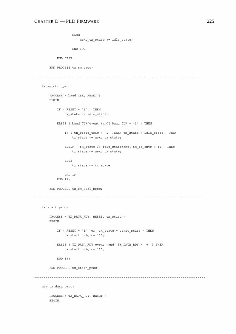
CHAPTER D — PLD FIRMWARE 225
ELSE
next_tx_state <= idle_state;
END IF;
END CASE;
END PROCESS tx_sm_proc;
------------------------------------------------------------------------------------------
tx_sm_ctrl_proc:
PROCESS ( baud_CLK, RESET )
BEGIN
IF ( RESET = ’1’ ) THEN
tx_state <= idle_state;
ELSIF ( baud_CLK’event )and( baud_CLK = ’1’ ) THEN
IF ( tx_start_trig = ’1’ )and( tx_state = idle_state ) THEN
tx_state <= next_tx_state;
ELSIF ( tx_state /= idle_state)and( tx_os_cntr = 15 ) THEN
tx_state <= next_tx_state;
ELSE
tx_state <= tx_state;
END IF;
END IF;
END PROCESS tx_sm_ctrl_proc;
------------------------------------------------------------------------------------------
tx_start_proc:
PROCESS ( TX_DATA_RDY, RESET, tx_state )
BEGIN
IF ( RESET = ’1’ )or( tx_state = start_state ) THEN
tx_start_trig <= ’0’;
ELSIF ( TX_DATA_RDY’event )and( TX_DATA_RDY = ’0’ ) THEN
tx_start_trig <= ’1’;
END IF;
END PROCESS tx_start_proc;
------------------------------------------------------------------------------------------
new_tx_data_proc:
PROCESS ( TX_DATA_RDY, RESET )
BEGIN

CHAPTER D — PLD FIRMWARE 226
IF ( RESET = ’1’ ) THEN
new_tx_data <= "00000000";
ELSIF ( TX_DATA_RDY’event )and( TX_DATA_RDY = ’0’ ) THEN
new_tx_data <= TX_DATA_IN;
END IF;
END PROCESS new_tx_data_proc;
END a;
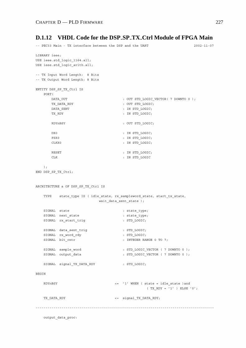
CHAPTER D — PLD FIRMWARE 227
D.1.12 VHDL Code for the DSP SP TX Ctrl Module of FPGA Main-- PEC33 Main - TX interface between the DSP and the UART 2002-11-07
LIBRARY ieee;
USE ieee.std_logic_1164.all;
USE ieee.std_logic_arith.all;
-- TX Input Word Length: 8 Bits
-- TX Output Word Length: 8 Bits
ENTITY DSP_SP_TX_Ctrl IS
PORT(
DATA_OUT : OUT STD_LOGIC_VECTOR( 7 DOWNTO 0 );
TX_DATA_RDY : OUT STD_LOGIC;
DATA_SENT : IN STD_LOGIC;
TX_RDY : IN STD_LOGIC;
RDYnBSY : OUT STD_LOGIC;
DX0 : IN STD_LOGIC;
FSX0 : IN STD_LOGIC;
CLKX0 : IN STD_LOGIC;
RESET : IN STD_LOGIC;
CLK : IN STD_LOGIC
);
END DSP_SP_TX_Ctrl;
ARCHITECTURE a OF DSP_SP_TX_Ctrl IS
TYPE state_type IS ( idle_state, rx_sampleword_state, start_tx_state,
wait_data_sent_state );
SIGNAL state : state_type;
SIGNAL next_state : state_type;
SIGNAL rx_start_trig : STD_LOGIC;
SIGNAL data_sent_trig : STD_LOGIC;
SIGNAL rx_word_rdy : STD_LOGIC;
SIGNAL bit_cntr : INTEGER RANGE 0 TO 7;
SIGNAL sample_word : STD_LOGIC_VECTOR ( 7 DOWNTO 0 );
SIGNAL output_data : STD_LOGIC_VECTOR ( 7 DOWNTO 0 );
SIGNAL signal_TX_DATA_RDY : STD_LOGIC;
BEGIN
RDYnBSY <= ’1’ WHEN ( state = idle_state )and
( TX_RDY = ’1’ ) ELSE ’0’;
TX_DATA_RDY <= signal_TX_DATA_RDY;
------------------------------------------------------------------------------------------
output_data_proc:

CHAPTER D — PLD FIRMWARE 228
PROCESS ( CLK, RESET )
BEGIN
IF ( RESET = ’1’ ) THEN
output_data <= "00000000";
ELSIF ( CLK’event )and( CLK = ’1’ ) THEN
output_data <= sample_word;
END IF;
END PROCESS output_data_proc;
------------------------------------------------------------------------------------------
data_sent_trig_proc:
PROCESS ( DATA_SENT, RESET, state )
BEGIN
IF ( RESET = ’1’ )or( state /= wait_data_sent_state ) THEN
data_sent_trig <= ’0’;
ELSIF ( DATA_SENT’event )and( DATA_SENT = ’0’ ) THEN
data_sent_trig <= ’1’;
END IF;
END PROCESS data_sent_trig_proc;
------------------------------------------------------------------------------------------
rx_proc:
PROCESS ( CLK, RESET )
BEGIN
IF ( RESET = ’1’ ) THEN
sample_word <= "00000000";
ELSIF ( CLK’event )and( CLK = ’0’ ) THEN
IF ( state = rx_sampleword_state)and( bit_cntr <= 7 ) THEN
sample_word( bit_cntr ) <= DX0;
ELSIF ( state = idle_state ) THEN
sample_word( bit_cntr ) <= sample_word( bit_cntr );
END IF;
END IF;
END PROCESS rx_proc;
------------------------------------------------------------------------------------------
sm_proc:
PROCESS ( state )
BEGIN
CASE state IS
WHEN idle_state =>
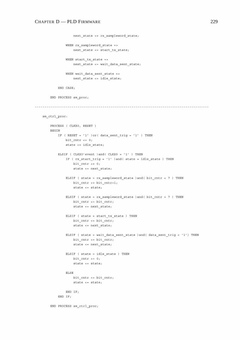
CHAPTER D — PLD FIRMWARE 229
next_state <= rx_sampleword_state;
WHEN rx_sampleword_state =>
next_state <= start_tx_state;
WHEN start_tx_state =>
next_state <= wait_data_sent_state;
WHEN wait_data_sent_state =>
next_state <= idle_state;
END CASE;
END PROCESS sm_proc;
------------------------------------------------------------------------------------------
sm_ctrl_proc:
PROCESS ( CLKX0, RESET )
BEGIN
IF ( RESET = ’1’ )or( data_sent_trig = ’1’ ) THEN
bit_cntr <= 0;
state <= idle_state;
ELSIF ( CLKX0’event )and( CLKX0 = ’1’ ) THEN
IF ( rx_start_trig = ’1’ )and( state = idle_state ) THEN
bit_cntr <= 0;
state <= next_state;
ELSIF ( state = rx_sampleword_state )and( bit_cntr < 7 ) THEN
bit_cntr <= bit_cntr+1;
state <= state;
ELSIF ( state = rx_sampleword_state )and( bit_cntr = 7 ) THEN
bit_cntr <= bit_cntr;
state <= next_state;
ELSIF ( state = start_tx_state ) THEN
bit_cntr <= bit_cntr;
state <= next_state;
ELSIF ( state = wait_data_sent_state )and( data_sent_trig = ’1’) THEN
bit_cntr <= bit_cntr;
state <= next_state;
ELSIF ( state = idle_state ) THEN
bit_cntr <= 0;
state <= state;
ELSE
bit_cntr <= bit_cntr;
state <= state;
END IF;
END IF;
END PROCESS sm_ctrl_proc;

CHAPTER D — PLD FIRMWARE 230
------------------------------------------------------------------------------------------
start_proc:
PROCESS ( FSX0, RESET )
BEGIN
IF ( RESET = ’1’ )or( state /= idle_state ) THEN
rx_start_trig <= ’0’;
ELSIF ( FSX0’event )and( FSX0 = ’1’ ) THEN
IF ( state = idle_state ) THEN
rx_start_trig <= ’1’;
END IF;
END IF;
END PROCESS start_proc;
------------------------------------------------------------------------------------------
tx_proc:
PROCESS ( CLK, RESET )
BEGIN
IF ( RESET = ’1’ ) THEN
signal_TX_DATA_RDY <= ’0’;
DATA_OUT <= "00000000";
ELSIF ( CLK’event )and( CLK = ’1’ ) THEN
IF ( state /= start_tx_state ) THEN
signal_TX_DATA_RDY <= ’0’;
DATA_OUT <= output_data;
ELSIF ( signal_TX_DATA_RDY = ’0’ ) THEN
signal_TX_DATA_RDY <= ’1’;
DATA_OUT <= output_data;
ELSE
signal_TX_DATA_RDY <= ’0’;
DATA_OUT <= output_data;
END IF;
END IF;
END PROCESS tx_proc;
END a;

CHAPTER D — PLD FIRMWARE 231
D.1.13 VHDL Code for the DSP SP RX Ctrl Module of FPGA Main-- PEC33 Main - RX interface between DSP serial port and UART 2002-11-07
-- Input Word Length: 8 Bits
-- Output Word Length: 32 Bits
LIBRARY ieee;
USE ieee.std_logic_1164.all;
USE ieee.std_logic_arith.all;
ENTITY DSP_SP_RX_Ctrl IS
PORT (
DATA_IN : IN STD_LOGIC_VECTOR( 7 DOWNTO 0 );
RX_DATA_RDY : IN STD_LOGIC;
DR0 : OUT STD_LOGIC;
FSR0 : OUT STD_LOGIC;
CLKR0 : OUT STD_LOGIC;
RESET : IN STD_LOGIC;
CLK : IN STD_LOGIC
);
END DSP_SP_RX_Ctrl;
ARCHITECTURE a OF DSP_SP_RX_Ctrl IS
TYPE rx_state_type IS ( idle_state, samplebyte_state, storeword_state );
TYPE tx_state_type IS ( idle_state, fs_state, tx_data_state );
SIGNAL rx_state : rx_state_type;
SIGNAL next_rx_state : rx_state_type;
SIGNAL tx_state : tx_state_type;
SIGNAL next_tx_state : tx_state_type;
SIGNAL rx_start_trig : STD_LOGIC;
SIGNAL tx_start_trig : STD_LOGIC;
SIGNAL rx_word_rdy : STD_LOGIC;
SIGNAL byte_cntr : INTEGER RANGE 0 TO 4;
SIGNAL bit_cntr : INTEGER RANGE 0 TO 32;
SIGNAL sample_word : STD_LOGIC_VECTOR ( 32 DOWNTO 0 );
SIGNAL slow_div_CLK : STD_LOGIC;
SIGNAL slow_CLK : STD_LOGIC;
BEGIN
CLKR0 <= slow_CLK;
------------------------------------------------------------------------------------------
rx_proc:
PROCESS ( CLK, RESET )
BEGIN
IF ( RESET = ’1’ ) THEN

CHAPTER D — PLD FIRMWARE 232
sample_word <= "000000000000000000000000000000000";
rx_word_rdy <= ’0’;
ELSIF ( CLK’event )and( CLK = ’1’ ) THEN
rx_word_rdy <= ’0’;
IF ( rx_state = samplebyte_state ) THEN
IF ( byte_cntr = 0 ) THEN
sample_word( 7 DOWNTO 0 ) <= DATA_IN;
ELSIF ( byte_cntr = 1 ) THEN
sample_word( 15 DOWNTO 8 ) <= DATA_IN;
ELSIF ( byte_cntr = 2 ) THEN
sample_word( 23 DOWNTO 16 ) <= DATA_IN;
ELSE
sample_word( 31 DOWNTO 24 ) <= DATA_IN;
END IF;
ELSIF ( rx_state = storeword_state) THEN
rx_word_rdy <= ’1’;
sample_word <= sample_word;
ELSIF ( rx_state = idle_state ) THEN
rx_word_rdy <= ’0’;
sample_word <= sample_word;
ELSE
rx_word_rdy <= rx_word_rdy;
sample_word <= sample_word;
END IF;
END IF;
END PROCESS rx_proc;
------------------------------------------------------------------------------------------
rx_sm_proc:
PROCESS ( rx_state )
BEGIN
CASE rx_state IS
WHEN idle_state =>
IF ( byte_cntr < 4 ) THEN
next_rx_state <= samplebyte_state;
ELSE
next_rx_state <= storeword_state;
END IF;
WHEN samplebyte_state =>
IF ( byte_cntr = 4 ) THEN
next_rx_state <= storeword_state;
ELSE

CHAPTER D — PLD FIRMWARE 233
next_rx_state <= idle_state;
END IF;
WHEN storeword_state =>
next_rx_state <= idle_state;
END CASE;
END PROCESS rx_sm_proc;
------------------------------------------------------------------------------------------
rx_sm_ctrl_proc:
PROCESS ( CLK, RESET )
BEGIN
IF ( RESET = ’1’ ) THEN
byte_cntr <= 0;
rx_state <= idle_state;
ELSIF ( CLK’event )and( CLK = ’1’ ) THEN
IF ( rx_start_trig = ’1’ )and( rx_state = idle_state ) THEN
byte_cntr <= byte_cntr;
rx_state <= next_rx_state;
ELSIF ( byte_cntr = 4 )and( rx_state = idle_state ) THEN
byte_cntr <= byte_cntr;
rx_state <= next_rx_state;
ELSIF ( rx_state = samplebyte_state )and( byte_cntr < 4 ) THEN
byte_cntr <= byte_cntr+1;
rx_state <= next_rx_state;
ELSIF ( rx_state = samplebyte_state )and( byte_cntr = 4 ) THEN
byte_cntr <= byte_cntr;
rx_state <= next_rx_state;
ELSIF ( rx_state = storeword_state ) THEN
byte_cntr <= 0;
rx_state <= next_rx_state;
ELSE
byte_cntr <= byte_cntr;
rx_state <= rx_state;
END IF;
END IF;
END PROCESS rx_sm_ctrl_proc;
------------------------------------------------------------------------------------------
rx_start_proc:
PROCESS ( RX_DATA_RDY, RESET )
BEGIN
IF ( RESET = ’1’ )or( rx_state /= idle_state ) THEN

CHAPTER D — PLD FIRMWARE 234
rx_start_trig <= ’0’;
ELSIF ( RX_DATA_RDY’event )and( RX_DATA_RDY = ’0’ ) THEN
IF ( rx_state = idle_state ) THEN
rx_start_trig <= ’1’;
ELSE
rx_start_trig <= ’0’;
END IF;
END IF;
END PROCESS rx_start_proc;
------------------------------------------------------------------------------------------
tx_proc:
PROCESS ( slow_CLK, RESET )
BEGIN
IF ( RESET = ’1’ ) THEN
FSR0 <= ’0’;
DR0 <= ’0’;
ELSIF ( slow_CLK’event )and( slow_CLK = ’1’ ) THEN
IF ( tx_state = fs_state ) THEN
FSR0 <= ’1’;
DR0 <= ’0’;
ELSIF ( tx_state = tx_data_state)and( bit_cntr < 32 ) THEN
FSR0 <= ’0’;
DR0 <= sample_word( bit_cntr );
ELSIF ( tx_state = tx_data_state)and( bit_cntr = 32 ) THEN
FSR0 <= ’0’;
DR0 <= ’0’;
ELSIF ( tx_state = idle_state ) THEN
FSR0 <= ’0’;
DR0 <= ’0’;
END IF;
END IF;
END PROCESS tx_proc;
------------------------------------------------------------------------------------------
tx_sm_proc:
PROCESS ( tx_state )
BEGIN
CASE tx_state IS
WHEN idle_state =>
next_tx_state <= fs_state;
WHEN fs_state =>
next_tx_state <= tx_data_state;

CHAPTER D — PLD FIRMWARE 235
WHEN tx_data_state =>
next_tx_state <= idle_state;
END CASE;
END PROCESS tx_sm_proc;
------------------------------------------------------------------------------------------
tx_sm_ctrl_proc:
PROCESS ( slow_CLK, RESET )
BEGIN
IF ( RESET = ’1’ ) THEN
bit_cntr <= 0;
tx_state <= idle_state;
ELSIF ( slow_CLK’event )and( slow_CLK = ’1’ ) THEN
IF ( tx_start_trig = ’1’ )and( tx_state = idle_state ) THEN
bit_cntr <= 0;
tx_state <= next_tx_state;
ELSIF ( tx_state = fs_state ) THEN
bit_cntr <= 0;
tx_state <= next_tx_state;
ELSIF ( tx_state = tx_data_state )and( bit_cntr < 32 ) THEN
bit_cntr <= bit_cntr+1;
tx_state <= tx_state;
ELSIF ( tx_state = tx_data_state )and( bit_cntr = 32 ) THEN
bit_cntr <= bit_cntr;
tx_state <= next_tx_state;
ELSIF ( tx_state = idle_state ) THEN
bit_cntr <= 0;
tx_state <= tx_state;
ELSE
bit_cntr <= bit_cntr;
tx_state <= tx_state;
END IF;
END IF;
END PROCESS tx_sm_ctrl_proc;
------------------------------------------------------------------------------------------
tx_start_proc:
PROCESS ( rx_word_rdy, RESET )
BEGIN
IF ( RESET = ’1’ )or( tx_state /= idle_state ) THEN
tx_start_trig <= ’0’;
ELSIF ( rx_word_rdy’event )and( rx_word_rdy = ’0’ ) THEN
IF ( tx_state = idle_state ) THEN
tx_start_trig <= ’1’;

CHAPTER D — PLD FIRMWARE 236
ELSE
tx_start_trig <= ’0’;
END IF;
END IF;
END PROCESS tx_start_proc;
------------------------------------------------------------------------------------------
slow_div_clk_proc:
PROCESS ( CLK, RESET )
BEGIN
IF ( RESET = ’1’ ) THEN
slow_div_CLK <= ’0’;
ELSIF ( CLK’event )and( CLK = ’0’ ) THEN
slow_div_CLK <= not slow_div_CLK;
END IF;
END PROCESS slow_div_clk_proc;
------------------------------------------------------------------------------------------
slow_clk_proc:
PROCESS ( slow_div_CLK, RESET )
BEGIN
IF ( RESET = ’1’ ) THEN
slow_CLK <= ’0’;
ELSIF ( slow_div_CLK’event )and( slow_div_CLK = ’1’ ) THEN
slow_CLK <= not slow_CLK;
END IF;
END PROCESS slow_clk_proc;
END a;
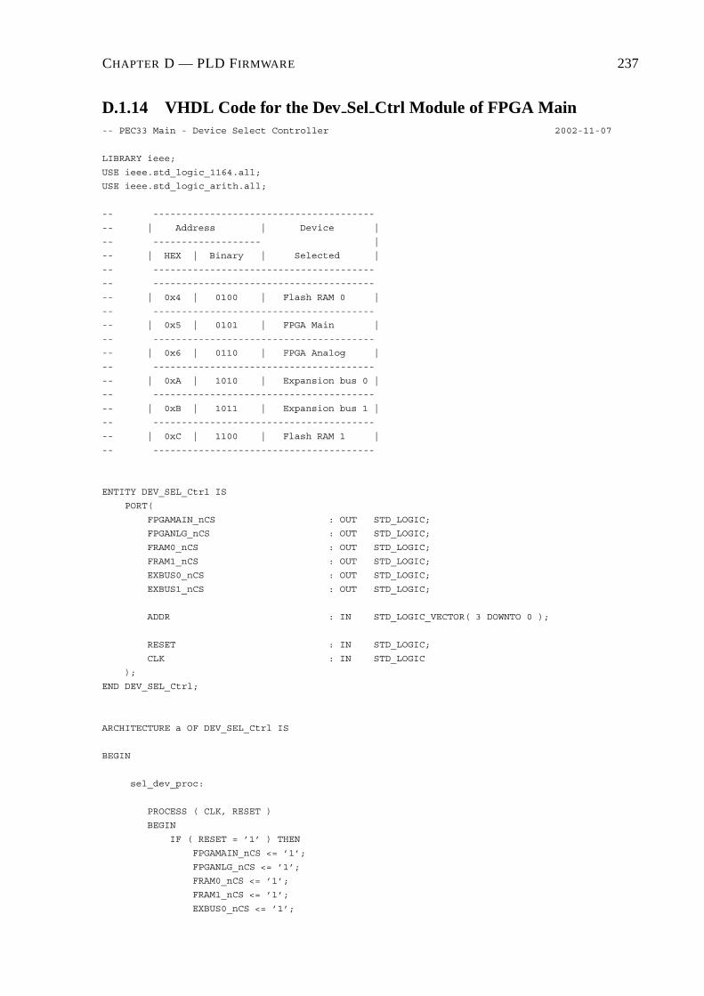
CHAPTER D — PLD FIRMWARE 237
D.1.14 VHDL Code for the Dev Sel Ctrl Module of FPGA Main-- PEC33 Main - Device Select Controller 2002-11-07
LIBRARY ieee;
USE ieee.std_logic_1164.all;
USE ieee.std_logic_arith.all;
-- ---------------------------------------
-- | Address | Device |
-- ------------------- |
-- | HEX | Binary | Selected |
-- ---------------------------------------
-- ---------------------------------------
-- | 0x4 | 0100 | Flash RAM 0 |
-- ---------------------------------------
-- | 0x5 | 0101 | FPGA Main |
-- ---------------------------------------
-- | 0x6 | 0110 | FPGA Analog |
-- ---------------------------------------
-- | 0xA | 1010 | Expansion bus 0 |
-- ---------------------------------------
-- | 0xB | 1011 | Expansion bus 1 |
-- ---------------------------------------
-- | 0xC | 1100 | Flash RAM 1 |
-- ---------------------------------------
ENTITY DEV_SEL_Ctrl IS
PORT(
FPGAMAIN_nCS : OUT STD_LOGIC;
FPGANLG_nCS : OUT STD_LOGIC;
FRAM0_nCS : OUT STD_LOGIC;
FRAM1_nCS : OUT STD_LOGIC;
EXBUS0_nCS : OUT STD_LOGIC;
EXBUS1_nCS : OUT STD_LOGIC;
ADDR : IN STD_LOGIC_VECTOR( 3 DOWNTO 0 );
RESET : IN STD_LOGIC;
CLK : IN STD_LOGIC
);
END DEV_SEL_Ctrl;
ARCHITECTURE a OF DEV_SEL_Ctrl IS
BEGIN
sel_dev_proc:
PROCESS ( CLK, RESET )
BEGIN
IF ( RESET = ’1’ ) THEN
FPGAMAIN_nCS <= ’1’;
FPGANLG_nCS <= ’1’;
FRAM0_nCS <= ’1’;
FRAM1_nCS <= ’1’;
EXBUS0_nCS <= ’1’;

CHAPTER D — PLD FIRMWARE 238
EXBUS1_nCS <= ’1’;
ELSIF ( CLK’event )and( CLK = ’1’ ) THEN
IF ( ADDR = "0100" ) THEN
FPGAMAIN_nCS <= ’1’;
FPGANLG_nCS <= ’1’;
FRAM0_nCS <= ’0’;
FRAM1_nCS <= ’1’;
EXBUS0_nCS <= ’1’;
EXBUS1_nCS <= ’1’;
ELSIF ( ADDR = "0101" ) THEN
FPGAMAIN_nCS <= ’0’;
FPGANLG_nCS <= ’1’;
FRAM0_nCS <= ’1’;
FRAM1_nCS <= ’1’;
EXBUS0_nCS <= ’1’;
EXBUS1_nCS <= ’1’;
ELSIF ( ADDR = "0110" ) THEN
FPGAMAIN_nCS <= ’1’;
FPGANLG_nCS <= ’0’;
FRAM0_nCS <= ’1’;
FRAM1_nCS <= ’1’;
EXBUS0_nCS <= ’1’;
EXBUS1_nCS <= ’1’;
ELSIF ( ADDR = "1010" ) THEN
FPGAMAIN_nCS <= ’1’;
FPGANLG_nCS <= ’1’;
FRAM0_nCS <= ’1’;
FRAM1_nCS <= ’1’;
EXBUS0_nCS <= ’0’;
EXBUS1_nCS <= ’1’;
ELSIF ( ADDR = "1011" ) THEN
FPGAMAIN_nCS <= ’1’;
FPGANLG_nCS <= ’1’;
FRAM0_nCS <= ’1’;
FRAM1_nCS <= ’1’;
EXBUS0_nCS <= ’1’;
EXBUS1_nCS <= ’0’;
ELSIF ( ADDR = "1100" ) THEN
FPGAMAIN_nCS <= ’1’;
FPGANLG_nCS <= ’1’;
FRAM0_nCS <= ’1’;
FRAM1_nCS <= ’0’;
EXBUS0_nCS <= ’1’;
EXBUS1_nCS <= ’1’;
ELSE
FPGAMAIN_nCS <= ’1’;
FPGANLG_nCS <= ’1’;
FRAM0_nCS <= ’1’;
FRAM1_nCS <= ’1’;
EXBUS0_nCS <= ’1’;
EXBUS1_nCS <= ’1’;

CHAPTER D — PLD FIRMWARE 239
END IF;
END IF;
END PROCESS sel_dev_proc;
END a;

CHAPTER D — PLD FIRMWARE 240
D.1.15 VHDL Code for the DSP Boot Ctrl Module of FPGA Main-- PEC33 Main - Reset & boot controller 2002-11-07
LIBRARY ieee;
USE ieee.std_logic_1164.all;
USE ieee.std_logic_arith.all;
-- The BOOT_TYPE input is from the DIP switch 1
-- -------------------------
-- | Value of | Boot data |
-- | BOOT_TYPE | source |
-- -------------------------
-- -------------------------
-- | 0 | Serial port |
-- -------------------------
-- | 1 | Flash RAM 0 |
-- -------------------------
ENTITY DSP_BOOT_Ctrl IS
PORT(
BOOT_TYPE : IN STD_LOGIC;
nINT1 : OUT STD_LOGIC;
nINT3 : OUT STD_LOGIC;
DSP_nRESET : OUT STD_LOGIC;
RESET : IN STD_LOGIC;
CLK : IN STD_LOGIC
);
END DSP_BOOT_Ctrl;
ARCHITECTURE a OF DSP_BOOT_Ctrl IS
TYPE state_type IS ( state0, state1, state2, state3, state4 );
SIGNAL signal_BOOT_TYPE : STD_LOGIC;
SIGNAL signal_DSP_nRESET : STD_LOGIC;
SIGNAL reset_trig : STD_LOGIC;
SIGNAL reset_cntr : INTEGER RANGE 0 TO 63;
SIGNAL int_cntr : INTEGER RANGE 0 TO 15;
SIGNAL dsp_resetting : STD_LOGIC;
SIGNAL state : state_type;
BEGIN
DSP_nRESET <= ’0’ WHEN ( state = state2 ) ELSE ’1’;
nINT1 <= ’0’ WHEN ( state = state4 )and( signal_BOOT_TYPE = ’0’ ) ELSE ’1’;
nINT3 <= ’0’ WHEN ( state = state4 )and( signal_BOOT_TYPE = ’1’ ) ELSE ’1’;
------------------------------------------------------------------------------------------
boot_type_proc:
PROCESS ( CLK )
BEGIN

CHAPTER D — PLD FIRMWARE 241
IF ( CLK’event )and( CLK = ’1’ ) THEN
signal_BOOT_TYPE <= BOOT_TYPE;
END IF;
END PROCESS boot_type_proc;
------------------------------------------------------------------------------------------
rst_dsp_trig_proc:
PROCESS ( RESET )
BEGIN
IF ( state = state1 ) THEN
reset_trig <= ’0’;
ELSIF ( RESET’event )and( RESET = ’0’ ) THEN
reset_trig <= ’1’;
END IF;
END PROCESS rst_dsp_trig_proc;
------------------------------------------------------------------------------------------
sm_ctrl_proc:
PROCESS ( CLK, RESET )
BEGIN
IF ( RESET = ’1’ ) THEN
state <= state0;
reset_cntr <= 0;
int_cntr <= 0;
ELSIF ( CLK’event )and( CLK = ’1’ ) THEN
IF ( reset_trig = ’1’ )and( state = state0 ) THEN
state <= state1;
reset_cntr <= 0;
int_cntr <= 0;
ELSIF ( state = state1 )and( reset_cntr < 10 ) THEN
state <= state;
reset_cntr <= reset_cntr+1;
int_cntr <= 0;
ELSIF ( state = state1 )and( reset_cntr = 10 ) THEN
state <= state2;
reset_cntr <= reset_cntr+1;
int_cntr <= int_cntr;
ELSIF ( state = state2 )and( reset_cntr < 60 ) THEN
state <= state;
reset_cntr <= reset_cntr+1;
int_cntr <= 0;
ELSIF ( state = state2 )and( reset_cntr = 60 ) THEN
state <= state3;
reset_cntr <= reset_cntr;
int_cntr <= int_cntr;

CHAPTER D — PLD FIRMWARE 242
ELSIF ( state = state3 )and( int_cntr < 7 ) THEN
state <= state;
reset_cntr <= 0;
int_cntr <= int_cntr+1;
ELSIF ( state = state3 )and( int_cntr = 7 ) THEN
state <= state4;
reset_cntr <= 0;
int_cntr <= int_cntr+1;
ELSIF ( state = state4 )and( int_cntr < 8 ) THEN
state <= state;
reset_cntr <= 0;
int_cntr <= int_cntr+1;
ELSIF ( state = state4 )and( int_cntr = 8 ) THEN
state <= state0;
reset_cntr <= 0;
int_cntr <= int_cntr;
ELSE
state <= state;
reset_cntr <= reset_cntr;
int_cntr <= int_cntr;
END IF;
END IF;
END PROCESS sm_ctrl_proc;
END a;

CHAPTER D — PLD FIRMWARE 243
D.1.16 VHDL Code for the Clk Gen Ctrl Module of FPGA Main-- PEC33 Main - Clock Generator 2002-11-07
LIBRARY ieee;
USE ieee.std_logic_1164.all;
USE ieee.std_logic_arith.all;
ENTITY CLK_GEN_Ctrl IS
PORT(
FPGANLG_CLK : OUT STD_LOGIC; -- 30MHz
DSP_CLK : OUT STD_LOGIC; -- 15MHz
EXBUS_CLK : OUT STD_LOGIC; -- 30MHz
RESET : IN STD_LOGIC;
CLK : IN STD_LOGIC
);
END CLK_GEN_Ctrl;
ARCHITECTURE a OF CLK_GEN_Ctrl IS
SIGNAL signal_dsp_clk : STD_LOGIC;
BEGIN
FPGANLG_CLK <= CLK;
DSP_CLK <= signal_dsp_clk;
EXBUS_CLK <= CLK;
------------------------------------------------------------------------------------------
dsp_clk_gen_proc:
PROCESS ( CLK, RESET )
BEGIN
IF ( CLK’event )and( CLK = ’1’ ) THEN
signal_dsp_clk <= not signal_dsp_clk;
END IF;
END PROCESS dsp_clk_gen_proc;
END a;

CHAPTER D — PLD FIRMWARE 244
D.2 Firmware for FPGA Analog

CHAPTER D — PLD FIRMWARE 245
D.2.1 Graphical Design File for FPGA Analog
ADC3_SAMP_CHAN7[2..0]ADC3_SAMP_CHAN6[2..0]
GLOBAL_RESET
ADC3_SAMP_CHAN5[2..0]ADC3_SAMP_CHAN4[2..0]ADC3_SAMP_CHAN3[2..0]ADC3_SAMP_CHAN2[2..0]
ADC3_CHAN[2..0]
ADC3_SAMP_CHAN1[2..0]ADC3_SAMP_CHAN0[2..0]ADC3_DATA_RDY
ADC3_DATA_VALIDGLOBAL_RESET
ADC3_DATA_RDYADC3_CHAN[2..0]ADC3_DATA_IN[9..0]
ADC3_DATA[12..0]
GLOBAL_CLKGLOBAL_RESET
ADC3_DATA_VALIDADC3_DATA_RDY
ADC_STATUS_IN3
ADC3_nENADC3_CHAN[2..0]ADC3_CONF_DATA[9..0]
ADC3_DATA_IN[9..0]
GLOBAL_RESET
ADC2_SAMP_CHAN5[2..0]ADC2_SAMP_CHAN6[2..0]ADC2_SAMP_CHAN7[2..0]
ADC2_SAMP_CHAN1[2..0]ADC2_SAMP_CHAN2[2..0]
ADC2_SAMP_CHAN4[2..0]ADC2_SAMP_CHAN3[2..0] ADC2_CHAN[2..0]
ADC2_SAMP_CHAN0[2..0]ADC2_DATA_RDY
ADC2_DATA_VALIDGLOBAL_RESET
ADC2_DATA[12..0]
ADC2_DATA_IN[9..0]ADC2_CHAN[2..0]ADC2_DATA_RDY
GLOBAL_RESETGLOBAL_CLK
ADC2_DATA_RDYADC2_DATA_VALID
ADC2_DATA_IN[9..0]
ADC_STATUS_IN2
ADC2_CONF_DATA[9..0]ADC2_CHAN[2..0]ADC2_nEN
GLOBAL_RESETADC1_SAMP_CHAN7[2..0]ADC1_SAMP_CHAN6[2..0]ADC1_SAMP_CHAN5[2..0]ADC1_SAMP_CHAN4[2..0]ADC1_SAMP_CHAN3[2..0]ADC1_SAMP_CHAN2[2..0]ADC1_SAMP_CHAN1[2..0]
ADC1_CHAN[2..0]
ADC1_SAMP_CHAN0[2..0]ADC1_DATA_RDY
ADC1_DATA_VALIDGLOBAL_RESET
ADC1_DATA_RDY ADC1_DATA[12..0]ADC1_CHAN[2..0]ADC1_DATA_IN[9..0]
GLOBAL_CLKGLOBAL_RESETADC1_nEN
ADC1_DATA_VALIDADC1_DATA_RDYADC1_DATA_IN[9..0]
ADC_STATUS_IN1
ADC1_CHAN[2..0]ADC1_CONF_DATA[9..0]
ADC0_SAMP_CHAN4[2..0]ADC0_SAMP_CHAN5[2..0]
GLOBAL_RESETADC0_SAMP_CHAN7[2..0]ADC0_SAMP_CHAN6[2..0]
ADC0_SAMP_CHAN0[2..0]ADC0_SAMP_CHAN1[2..0]
ADC0_SAMP_CHAN3[2..0]ADC0_SAMP_CHAN2[2..0]
ADC0_CHAN[2..0]
ADC0_DATA_RDY
ADC0_DATA_VALIDGLOBAL_RESET
ADC0_DATA_RDYADC0_CHAN[2..0]
ADC0_DATA[12..0]
ADC0_DATA_IN[9..0]
ADC0_CHAN[2..0]ADC0_nENGLOBAL_RESETGLOBAL_CLK ADC0_DATA_VALID
ADC0_DATA_RDYADC0_DATA_IN[9..0]
ADC_STATUS_IN0
ADC0_CONF_DATA[9..0]
AND2
pec33_analog_ver4@184ADC3_SDOUT INPUT
pec33_analog_ver4@190ADC3_SCLKOUTPUTpec33_analog_ver4@187ADC3_nCSOUTPUTpec33_analog_ver4@189ADC3_SDINOUTPUT
AND2
pec33_analog_ver4@182ADC2_SDOUT INPUT pec33_analog_ver4@176ADC2_SDINOUTPUT
pec33_analog_ver4@179ADC2_nCSOUTPUT
pec33_analog_ver4@177ADC2_SCLKOUTPUT
AND2
pec33_analog_ver4@174ADC1_SDOUT INPUT
pec33_analog_ver4@175ADC1_nCSOUTPUTpec33_analog_ver4@172ADC1_SDINOUTPUT
pec33_analog_ver4@173ADC1_SCLKOUTPUT
pec33_analog_ver4@168ADC0_SCLKOUTPUT
AND2
pec33_analog_ver4@169ADC0_SDOUT INPUT
pec33_analog_ver4@170ADC0_nCSOUTPUTpec33_analog_ver4@167ADC0_SDINOUTPUT
Figure D.5: Graphical Design File of FPGA Analog (Part 1 of 5)

CHAPTER D — PLD FIRMWARE 246
GLOBAL_RESETGLOBAL_CLK
KP_ROW[3..0] KP_COL[2..0]KEYVAL[3..0]
GLOBAL_RESETINT_EN[14..0]PWM1_COUNTERZERO
GLOBAL_CLK
PWM1_COMPDOWNPWM1_COMPUPPWM0_COUNTERZERO
PWM1_RAMPDIR
PWM_ERR_BOT_OUT[8..0]PWM_STATUS_OUT[7..0]INT_REG[5..0]
PWM_ERR_TOP[8..0]PWM_ERR_BOT[8..0]PWM0_COMPUPPWM0_COMPDOWNPWM0_RAMPDIR
KEYVAL_OUT[3..0]ADC_STATUS_OUT[3..0]
PWM_ERR_TOP_OUT[8..0]
ADC_STATUS_IN[3..0]KEYVAL[3..0]
GLOBAL_CLKGLOBAL_RESET
DAC3_B_DATA[11..0]DAC3_CTRL_DATA[1..0]DAC3_nLOAD
DAC3_B_CONF_DATA[2..0]DAC3_A_DATA[11..0]DAC3_A_CONF_DATA[2..0]
GLOBAL_RESETGLOBAL_CLK
DAC2_nLOADDAC2_CTRL_DATA[1..0]
DAC2_B_CONF_DATA[2..0]DAC2_B_DATA[11..0]
DAC2_A_DATA[11..0]DAC2_A_CONF_DATA[2..0]
GLOBAL_CLK
DAC1_CTRL_DATA[1..0]DAC1_nLOADGLOBAL_RESET
DAC1_B_DATA[11..0]DAC1_B_CONF_DATA[2..0]
DAC1_A_CONF_DATA[2..0]DAC1_A_DATA[11..0]
GLOBAL_CLKGLOBAL_RESETDAC0_nLOAD
DAC0_B_DATA[11..0]DAC0_CTRL_DATA[1..0]
DAC0_B_CONF_DATA[2..0]DAC0_A_DATA[11..0]DAC0_A_CONF_DATA[2..0]
pec33_analog_ver4@142KP_COL2OUTPUT
pec33_analog_ver4@140 KP_ROW1 INPUT
pec33_analog_ver4@139 KP_ROW2 INPUT
pec33_analog_ver4@136 KP_ROW3 INPUT pec33_analog_ver4@144KP_COL0OUTPUT
pec33_analog_ver4@143KP_COL1OUTPUT
pec33_analog_ver4@141 KP_ROW0 INPUT
pec33_analog_ver4@83DSP_nINT2OUTPUTpec33_analog_ver4@85DSP_nINT0OUTPUT
pec33_analog_ver4@206DAC3_nSYNCOUTPUT
pec33_analog_ver4@207DAC3_SCLKOUTPUT
pec33_analog_ver4@205DAC3_nLDACOUTPUT
pec33_analog_ver4@208DAC3_SDINOUTPUT
pec33_analog_ver4@204DAC2_SDINOUTPUT
pec33_analog_ver4@202DAC2_nSYNCOUTPUT
pec33_analog_ver4@200DAC2_nLDACOUTPUTpec33_analog_ver4@203DAC2_SCLKOUTPUT
pec33_analog_ver4@198DAC1_SCLKOUTPUT
pec33_analog_ver4@196DAC1_nLDACOUTPUT
pec33_analog_ver4@197DAC1_nSYNCOUTPUTpec33_analog_ver4@199DAC1_SDINOUTPUT
pec33_analog_ver4@192DAC0_nSYNCOUTPUT
pec33_analog_ver4@193DAC0_SCLKOUTPUT
pec33_analog_ver4@191DAC0_nLDACOUTPUT
pec33_analog_ver4@195DAC0_SDINOUTPUT
Figure D.6: Graphical Design File of FPGA Analog (Part 2 of 5)

CHAPTER D — PLD FIRMWARE 247
CMD_REG1_EN
INT_REG_EN
CMD_REG0_ENINT_EN_EN
PWM_ERR_BOT_EN
PWM1_DOWNVAL_ENPWM_ERR_TOP_EN
PWM1_UPVAL_ENPWM1_DEADTIME_EN
PWM1_REFC_EN
PWM1_TRIFREQSCALE_ENPWM1_TRIMAX_ENPWM1_REFN_EN
PWM1_REFB_EN
PWM0_UPVAL_ENPWM0_DOWNVAL_ENPWM1_REFA_EN
PWM0_REFN_ENPWM0_TRIMAX_ENPWM0_TRIFREQSCALE_ENPWM0_DEADTIME_EN
PWM_STATUS_ENPWM0_REFA_ENPWM0_REFB_ENPWM0_REFC_EN
LCD_CHAR_ENLCD_ADDR_ENLCD_STATUS_ENKEYVAL_EN
ADC3_SAMP_CHAN5_ENADC3_SAMP_CHAN6_ENADC3_SAMP_CHAN7_ENLCD_MODE_EN
ADC3_SAMP_CHAN1_ENADC3_SAMP_CHAN2_ENADC3_SAMP_CHAN3_ENADC3_SAMP_CHAN4_EN
ADC2_SAMP_CHAN7_ENADC3_CONF_ENADC3_DATA_ENADC3_SAMP_CHAN0_EN
DSP_H3
GLOBAL_RESET ADC2_SAMP_CHAN3_ENADC2_SAMP_CHAN4_ENADC2_SAMP_CHAN5_ENADC2_SAMP_CHAN6_EN
ADDR[9..0] ADC2_SAMP_CHAN0_ENADC2_DATA_EN
ADC2_SAMP_CHAN1_ENADC2_SAMP_CHAN2_EN
ADC2_CONF_EN
ADC1_SAMP_CHAN5_ENADC1_SAMP_CHAN6_ENADC1_SAMP_CHAN7_EN
ADC1_SAMP_CHAN3_EN
ADC1_SAMP_CHAN1_ENADC1_SAMP_CHAN2_EN
ADC1_SAMP_CHAN4_EN
ADC0_SAMP_CHAN7_ENADC1_CONF_ENADC1_DATA_ENADC1_SAMP_CHAN0_EN
ADC0_SAMP_CHAN3_ENADC0_SAMP_CHAN4_ENADC0_SAMP_CHAN5_ENADC0_SAMP_CHAN6_EN
ADC0_SAMP_CHAN0_ENADC0_DATA_EN
ADC0_SAMP_CHAN1_ENADC0_SAMP_CHAN2_EN
ADC0_CONF_EN
DAC3_B_CONF_ENDAC3_B_DATA_ENADC_STATUS_EN
DAC2_B_DATA_ENDAC3_CTRL_ENDAC3_A_CONF_ENDAC3_A_DATA_EN
DAC2_A_CONF_EN
DAC2_B_CONF_EN
DAC2_CTRL_EN
DAC2_A_DATA_EN
DAC1_A_CONF_EN
DAC1_B_CONF_ENDAC1_A_DATA_EN
DAC1_B_DATA_EN
DAC0_A_DATA_ENDAC0_B_CONF_ENDAC0_B_DATA_ENDAC1_CTRL_EN
DAC0_A_CONF_ENDAC0_CTRL_EN
LCD_RESET
PWM1_nENPWM0_nEN
CMD_REG1[5..0]GLOBAL_RESETGLOBAL_CLK
ADC2_nENADC3_nEN
LCD_UPDATE_DATALCD_UPDATE_MODE
CMD_REG0[6..0] ADC0_nEN
DAC2_nLOAD
ADC1_nEN
DAC3_nLOAD
DAC1_nLOADDAC0_nLOAD
pec33_analog_ver4@79 GLOBAL_CLK INPUT
pec33_analog_ver4@78 DSP_nSTRB INPUT
pec33_analog_ver4@75FPGA_nRESET INPUTNOT
pec33_analog_ver4@92 ADDR8 INPUT
pec33_analog_ver4@90 ADDR9 INPUT
pec33_analog_ver4@74 FPGA_nCS INPUT
pec33_analog_ver4@96 ADDR4 INPUT
pec33_analog_ver4@95 ADDR5 INPUT
pec33_analog_ver4@94 ADDR6 INPUT
pec33_analog_ver4@93 ADDR7 INPUT
pec33_analog_ver4@101 ADDR0 INPUT
pec33_analog_ver4@100 ADDR1 INPUT
pec33_analog_ver4@99 ADDR2 INPUT
pec33_analog_ver4@97 ADDR3 INPUT
Figure D.7: Graphical Design File of FPGA Analog (Part 3 of 5)

CHAPTER D — PLD FIRMWARE 248
DSP_H3GLOBAL_RESETCMD_REG1_ENCMD_REG0_EN
INT_EN_ENPWM_ERR_BOT_EN
INT_REG_EN
PWM_ERR_TOP_ENPWM1_DOWNVAL_ENPWM1_UPVAL_ENPWM1_DEADTIME_ENPWM1_TRIFREQSCALE_ENPWM1_TRIMAX_ENPWM1_REFN_ENPWM1_REFC_ENPWM1_REFB_ENPWM1_REFA_ENPWM0_DOWNVAL_ENPWM0_UPVAL_EN
DATA[15..0]RnWCMD_REG1[5..0]CMD_REG0[6..0]PWM0_DEADTIME_EN
PWM0_TRIFREQSCALE_ENPWM0_TRIMAX_ENPWM0_REFN_EN
INT_EN[14..0]PWM1_COMPDOWNVAL[9..0]PWM1_COMPUPVAL[9..0]PWM1_DEADTIME[9..0]PWM0_REFC_EN
PWM0_REFB_ENPWM0_REFA_ENPWM_STATUS_EN
PWM1_TRIFREQSCALE[9..0]PWM1_TRIMAX[9..0]PWM1_REFN[9..0]PWM1_REFC[9..0]KEYVAL_EN
LCD_STATUS_ENLCD_ADDR_ENLCD_CHAR_EN
PWM1_REFB[9..0]PWM1_REFA[9..0]PWM0_COMPDOWNVAL[9..0]PWM0_COMPUPVAL[9..0]LCD_MODE_EN
ADC3_SAMP_CHAN7_ENADC3_SAMP_CHAN6_ENADC3_SAMP_CHAN5_EN
PWM0_DEADTIME[9..0]PWM0_TRIFREQSCALE[9..0]PWM0_TRIMAX[9..0]PWM0_REFN[9..0]ADC3_SAMP_CHAN4_EN
ADC3_SAMP_CHAN3_ENADC3_SAMP_CHAN2_ENADC3_SAMP_CHAN1_EN
PWM0_REFC[9..0]PWM0_REFB[9..0]PWM0_REFA[9..0]LCD_ADDR[6..0]ADC3_SAMP_CHAN0_EN
ADC3_DATA_ENADC3_CONF_ENADC2_SAMP_CHAN7_EN
LCD_CHAR[7..0]LCD_MODE_DATA[7..0]ADC3_SAMP_CHAN7[2..0]ADC3_SAMP_CHAN6[2..0]ADC2_SAMP_CHAN6_EN
ADC2_SAMP_CHAN5_ENADC2_SAMP_CHAN4_ENADC2_SAMP_CHAN3_EN
ADC3_SAMP_CHAN5[2..0]ADC3_SAMP_CHAN4[2..0]ADC3_SAMP_CHAN3[2..0]ADC3_SAMP_CHAN2[2..0]ADC2_SAMP_CHAN2_EN
ADC2_SAMP_CHAN1_ENADC2_SAMP_CHAN0_ENADC2_DATA_EN
ADC3_SAMP_CHAN1[2..0]ADC3_SAMP_CHAN0[2..0]ADC3_CONF_DATA[9..0]ADC2_SAMP_CHAN7[2..0]ADC2_CONF_EN
ADC1_SAMP_CHAN7_ENADC1_SAMP_CHAN6_ENADC1_SAMP_CHAN5_EN
ADC2_SAMP_CHAN6[2..0]ADC2_SAMP_CHAN5[2..0]ADC2_SAMP_CHAN4[2..0]ADC2_SAMP_CHAN3[2..0]ADC1_SAMP_CHAN4_EN
ADC1_SAMP_CHAN3_ENADC1_SAMP_CHAN2_ENADC1_SAMP_CHAN1_EN
ADC2_SAMP_CHAN2[2..0]ADC2_SAMP_CHAN1[2..0]ADC2_SAMP_CHAN0[2..0]ADC2_CONF_DATA[9..0]ADC1_SAMP_CHAN0_EN
ADC1_DATA_ENADC1_CONF_ENADC0_SAMP_CHAN7_EN
ADC1_SAMP_CHAN7[2..0]ADC1_SAMP_CHAN6[2..0]ADC1_SAMP_CHAN5[2..0]ADC1_SAMP_CHAN4[2..0]ADC0_SAMP_CHAN6_EN
ADC0_SAMP_CHAN5_ENADC0_SAMP_CHAN4_ENADC0_SAMP_CHAN3_EN
ADC1_SAMP_CHAN3[2..0]ADC1_SAMP_CHAN2[2..0]ADC1_SAMP_CHAN1[2..0]ADC1_SAMP_CHAN0[2..0]ADC0_SAMP_CHAN2_EN
ADC0_SAMP_CHAN1_ENADC0_SAMP_CHAN0_EN
ADC0_DATA_EN
ADC1_CONF_DATA[9..0]ADC0_SAMP_CHAN7[2..0]ADC0_SAMP_CHAN6[2..0]ADC0_SAMP_CHAN5[2..0]ADC0_CONF_EN
ADC_STATUS_ENDAC3_B_DATA_ENDAC3_B_CONF_EN
ADC0_SAMP_CHAN4[2..0]ADC0_SAMP_CHAN3[2..0]ADC0_SAMP_CHAN2[2..0]ADC0_SAMP_CHAN1[2..0]DAC3_A_DATA_EN
DAC3_A_CONF_ENDAC3_CTRL_ENDAC2_B_DATA_EN
ADC0_SAMP_CHAN0[2..0]ADC0_CONF_DATA[9..0]DAC3_B_CONF_DATA[2..0]DAC3_B_DATA[11..0]DAC2_B_CONF_EN
DAC2_A_DATA_ENDAC2_A_CONF_ENDAC2_CTRL_EN
DAC3_A_CONF_DATA[2..0]DAC3_A_DATA[11..0]DAC3_CTRL_DATA[1..0]DAC2_B_CONF_DATA[2..0]DAC1_B_DATA_EN
DAC1_B_CONF_ENDAC1_A_DATA_ENDAC1_A_CONF_EN
DAC2_B_DATA[11..0]DAC2_A_CONF_DATA[2..0]DAC2_A_DATA[11..0]DAC2_CTRL_DATA[1..0]DAC1_CTRL_EN
DAC0_B_DATA_ENDAC0_B_CONF_ENDAC0_A_DATA_EN
DAC1_B_CONF_DATA[2..0]DAC1_B_DATA[11..0]DAC1_A_CONF_DATA[2..0]DAC1_A_DATA[11..0]DAC0_A_CONF_EN
DAC0_CTRL_EN
PWM_ERR_BOT_OUT[8..0]PWM_ERR_TOP_OUT[8..0]
INT_REG[5..0]DAC1_CTRL_DATA[1..0]DAC0_B_CONF_DATA[2..0]DAC0_B_DATA[11..0]DAC0_A_CONF_DATA[2..0]
PWM_STATUS_OUT7PWM_STATUS_OUT6PWM_STATUS_OUT5
DAC0_A_DATA[11..0]DAC0_CTRL_DATA[1..0]
PWM_STATUS_OUT4PWM_STATUS_OUT3PWM_STATUS_OUT2PWM_STATUS_OUT1
KEYVAL_OUT[3..0]PWM_STATUS_OUT0
LCD_RDYnBSYADC_STATUS_OUT3ADC3_DATA[12..0]ADC_STATUS_OUT2ADC2_DATA[12..0]ADC_STATUS_OUT1ADC1_DATA[12..0]ADC_STATUS_OUT0ADC0_DATA[12..0]
pec33_analog_ver4@37DATA12BIDIR
pec33_analog_ver4@36DATA13BIDIR
pec33_analog_ver4@31DATA14BIDIR
pec33_analog_ver4@30DATA15BIDIR
pec33_analog_ver4@41DATA8BIDIR
pec33_analog_ver4@40DATA9BIDIR
pec33_analog_ver4@39DATA10BIDIR
pec33_analog_ver4@38DATA11BIDIR
pec33_analog_ver4@47DATA4BIDIR
pec33_analog_ver4@46DATA5BIDIR
pec33_analog_ver4@45DATA6BIDIR
pec33_analog_ver4@44DATA7BIDIR
pec33_analog_ver4@86DATA0BIDIR
pec33_analog_ver4@87DATA1BIDIR
pec33_analog_ver4@88DATA2BIDIR
pec33_analog_ver4@89DATA3BIDIR
Figure D.8: Graphical Design File of FPGA Analog (Part 4 of 5)

CHAPTER D — PLD FIRMWARE 249
PWM0_COUNTERZERO
DAC0_nLDAC
GLOBAL_CLKGLOBAL_RESET
INT_EN0
INT_REG4
INT_REG0
DSP_nINT0
PWM0_COMPDOWN
GLOBAL_CLKGLOBAL_RESETPWM1_nENPWM1_COMPDOWNVAL[9..0]PWM1_COMPUPVAL[9..0]PWM1_REFN[9..0]
PWM1_COUNTERZEROPWM1_RAMPDIR
PWM1_REFC[9..0]PWM1_REFB[9..0]PWM1_REFA[9..0]PWM1_DEADTIME[9..0]
PWM1_COMPDOWNPWM1_COMPUP
PWM1_TRIFREQSCALE[9..0]PWM1_TRIMAX[9..0]
GLOBAL_CLKGLOBAL_RESETPWM0_nENPWM0_COMPDOWNVAL[9..0]PWM0_COMPUPVAL[9..0]PWM0_REFN[9..0]PWM0_REFC[9..0]
PWM0_COUNTERZEROPWM0_RAMPDIR
PWM0_REFB[9..0]PWM0_REFA[9..0]PWM0_DEADTIME[9..0]PWM0_TRIFREQSCALE[9..0]
PWM0_COMPDOWNPWM0_COMPUP
PWM0_TRIMAX[9..0]
GLOBAL_CLKGLOBAL_RESETLCD_RESETLCD_UPDATE_DATALCD_ADDR[6..0]LCD_CHAR[7..0]
LCD_RDYnBSY
LCD_UPDATE_MODELCD_MODE_DATA[7..0]
LCD_DATA[7..0]
GND pec33_analog_ver4@183DSP_H3INPUT
NOTpec33_analog_ver4@61LED7OUTPUT
pec33_analog_ver4@80DSP_RnWINPUT
NOTpec33_analog_ver4@60LED6OUTPUT
NOT
NOTpec33_analog_ver4@57LED4OUTPUT
pec33_analog_ver4@58LED5OUTPUT
NOT
NOT
pec33_analog_ver4@56LED3OUTPUT
NOT
pec33_analog_ver4@55LED2OUTPUT
pec33_analog_ver4@54LED1OUTPUT
NOTpec33_analog_ver4@53LED0OUTPUT
pec33_analog_ver4@16 PWM_ERR_BOT8 INPUTpec33_analog_ver4@15 PWM_ERR_TOP8 INPUT
pec33_analog_ver4@125PWM_DC_BOTOUTPUTpec33_analog_ver4@122PWM_DC_TOPOUTPUT
VCC
pec33_analog_ver4@113PWM1_N_BOTOUTPUT
pec33_analog_ver4@115PWM1_C_BOTOUTPUT
pec33_analog_ver4@112PWM1_N_TOPOUTPUT
pec33_analog_ver4@28 PWM_ERR_TOP7 INPUT
pec33_analog_ver4@29 PWM_ERR_BOT7 INPUT pec33_analog_ver4@119PWM1_B_BOTOUTPUT
pec33_analog_ver4@114PWM1_C_TOPOUTPUT
pec33_analog_ver4@24 PWM_ERR_TOP5 INPUT
pec33_analog_ver4@25 PWM_ERR_BOT5 INPUT
pec33_analog_ver4@27 PWM_ERR_BOT6 INPUTpec33_analog_ver4@26 PWM_ERR_TOP6 INPUT
pec33_analog_ver4@121PWM1_A_BOTOUTPUT
pec33_analog_ver4@116PWM1_B_TOPOUTPUT
pec33_analog_ver4@18 PWM_ERR_BOT4 INPUTpec33_analog_ver4@17 PWM_ERR_TOP4 INPUT
pec33_analog_ver4@120PWM1_A_TOPOUTPUT
pec33_analog_ver4@127PWM0_N_BOTOUTPUT
pec33_analog_ver4@131PWM0_C_BOTOUTPUT
pec33_analog_ver4@126PWM0_N_TOPOUTPUT
pec33_analog_ver4@14 PWM_ERR_BOT3 INPUTpec33_analog_ver4@13 PWM_ERR_TOP3 INPUTpec33_analog_ver4@12 PWM_ERR_BOT2 INPUT
pec33_analog_ver4@133PWM0_B_BOTOUTPUT
pec33_analog_ver4@128PWM0_C_TOPOUTPUT
pec33_analog_ver4@10 PWM_ERR_BOT1 INPUTpec33_analog_ver4@9 PWM_ERR_TOP1 INPUTpec33_analog_ver4@8 PWM_ERR_BOT0 INPUT
pec33_analog_ver4@11 PWM_ERR_TOP2 INPUT
pec33_analog_ver4@135PWM0_A_BOTOUTPUT
pec33_analog_ver4@132PWM0_B_TOPOUTPUT
pec33_analog_ver4@7 PWM_ERR_TOP0 INPUTpec33_analog_ver4@134PWM0_A_TOPOUTPUT
pec33_analog_ver4@149LCD_EOUTPUT
pec33_analog_ver4@148LCD_RnWOUTPUT
pec33_analog_ver4@147LCD_RSOUTPUT
pec33_analog_ver4@162LCD_DATA6BIDIRpec33_analog_ver4@161LCD_DATA5BIDIR
pec33_analog_ver4@163LCD_DATA7BIDIR
pec33_analog_ver4@158LCD_DATA2BIDIRpec33_analog_ver4@157LCD_DATA1BIDIR
pec33_analog_ver4@160LCD_DATA4BIDIRpec33_analog_ver4@159LCD_DATA3BIDIR
pec33_analog_ver4@150LCD_DATA0BIDIR
Figure D.9: Graphical Design File of FPGA Analog (Part 5 of 5)

CHAPTER D — PLD FIRMWARE 250
D.2.2 VHDL Code for the Addr Dec Ctrl Module of FPGA Analog-- FPGA Analog - Address Decoder Controller 2002-10-21
LIBRARY ieee;
USE ieee.std_logic_1164.all;
USE ieee.std_logic_arith.all;
ENTITY Addr_Dec_Ctrl IS
PORT (
DAC0_CTRL_EN : OUT STD_LOGIC;
DAC0_A_CONF_EN : OUT STD_LOGIC;
DAC0_A_DATA_EN : OUT STD_LOGIC;
DAC0_B_CONF_EN : OUT STD_LOGIC;
DAC0_B_DATA_EN : OUT STD_LOGIC;
DAC1_CTRL_EN : OUT STD_LOGIC;
DAC1_A_CONF_EN : OUT STD_LOGIC;
DAC1_A_DATA_EN : OUT STD_LOGIC;
DAC1_B_CONF_EN : OUT STD_LOGIC;
DAC1_B_DATA_EN : OUT STD_LOGIC;
DAC2_CTRL_EN : OUT STD_LOGIC;
DAC2_A_CONF_EN : OUT STD_LOGIC;
DAC2_A_DATA_EN : OUT STD_LOGIC;
DAC2_B_CONF_EN : OUT STD_LOGIC;
DAC2_B_DATA_EN : OUT STD_LOGIC;
DAC3_CTRL_EN : OUT STD_LOGIC;
DAC3_A_CONF_EN : OUT STD_LOGIC;
DAC3_A_DATA_EN : OUT STD_LOGIC;
DAC3_B_CONF_EN : OUT STD_LOGIC;
DAC3_B_DATA_EN : OUT STD_LOGIC;
ADC_STATUS_EN : OUT STD_LOGIC;
ADC0_CONF_EN : OUT STD_LOGIC;
ADC0_DATA_EN : OUT STD_LOGIC;
ADC0_SAMP_CHAN0_EN : OUT STD_LOGIC;
ADC0_SAMP_CHAN1_EN : OUT STD_LOGIC;
ADC0_SAMP_CHAN2_EN : OUT STD_LOGIC;
ADC0_SAMP_CHAN3_EN : OUT STD_LOGIC;
ADC0_SAMP_CHAN4_EN : OUT STD_LOGIC;
ADC0_SAMP_CHAN5_EN : OUT STD_LOGIC;
ADC0_SAMP_CHAN6_EN : OUT STD_LOGIC;
ADC0_SAMP_CHAN7_EN : OUT STD_LOGIC;
ADC1_CONF_EN : OUT STD_LOGIC;
ADC1_DATA_EN : OUT STD_LOGIC;
ADC1_SAMP_CHAN0_EN : OUT STD_LOGIC;
ADC1_SAMP_CHAN1_EN : OUT STD_LOGIC;
ADC1_SAMP_CHAN2_EN : OUT STD_LOGIC;
ADC1_SAMP_CHAN3_EN : OUT STD_LOGIC;
ADC1_SAMP_CHAN4_EN : OUT STD_LOGIC;
ADC1_SAMP_CHAN5_EN : OUT STD_LOGIC;
ADC1_SAMP_CHAN6_EN : OUT STD_LOGIC;
ADC1_SAMP_CHAN7_EN : OUT STD_LOGIC;
ADC2_CONF_EN : OUT STD_LOGIC;
ADC2_DATA_EN : OUT STD_LOGIC;
ADC2_SAMP_CHAN0_EN : OUT STD_LOGIC;
ADC2_SAMP_CHAN1_EN : OUT STD_LOGIC;

CHAPTER D — PLD FIRMWARE 251
ADC2_SAMP_CHAN2_EN : OUT STD_LOGIC;
ADC2_SAMP_CHAN3_EN : OUT STD_LOGIC;
ADC2_SAMP_CHAN4_EN : OUT STD_LOGIC;
ADC2_SAMP_CHAN5_EN : OUT STD_LOGIC;
ADC2_SAMP_CHAN6_EN : OUT STD_LOGIC;
ADC2_SAMP_CHAN7_EN : OUT STD_LOGIC;
ADC3_CONF_EN : OUT STD_LOGIC;
ADC3_DATA_EN : OUT STD_LOGIC;
ADC3_SAMP_CHAN0_EN : OUT STD_LOGIC;
ADC3_SAMP_CHAN1_EN : OUT STD_LOGIC;
ADC3_SAMP_CHAN2_EN : OUT STD_LOGIC;
ADC3_SAMP_CHAN3_EN : OUT STD_LOGIC;
ADC3_SAMP_CHAN4_EN : OUT STD_LOGIC;
ADC3_SAMP_CHAN5_EN : OUT STD_LOGIC;
ADC3_SAMP_CHAN6_EN : OUT STD_LOGIC;
ADC3_SAMP_CHAN7_EN : OUT STD_LOGIC;
LCD_MODE_EN : OUT STD_LOGIC;
LCD_CHAR_EN : OUT STD_LOGIC;
LCD_ADDR_EN : OUT STD_LOGIC;
LCD_STATUS_EN : OUT STD_LOGIC;
KEYVAL_EN : OUT STD_LOGIC;
PWM_STATUS_EN : OUT STD_LOGIC;
PWM0_REFA_EN : OUT STD_LOGIC;
PWM0_REFB_EN : OUT STD_LOGIC;
PWM0_REFC_EN : OUT STD_LOGIC;
PWM0_REFN_EN : OUT STD_LOGIC;
PWM0_TRIMAX_EN : OUT STD_LOGIC;
PWM0_TRIFREQSCALE_EN : OUT STD_LOGIC;
PWM0_DEADTIME_EN : OUT STD_LOGIC;
PWM0_UPVAL_EN : OUT STD_LOGIC;
PWM0_DOWNVAL_EN : OUT STD_LOGIC;
PWM1_REFA_EN : OUT STD_LOGIC;
PWM1_REFB_EN : OUT STD_LOGIC;
PWM1_REFC_EN : OUT STD_LOGIC;
PWM1_REFN_EN : OUT STD_LOGIC;
PWM1_TRIMAX_EN : OUT STD_LOGIC;
PWM1_TRIFREQSCALE_EN : OUT STD_LOGIC;
PWM1_DEADTIME_EN : OUT STD_LOGIC;
PWM1_UPVAL_EN : OUT STD_LOGIC;
PWM1_DOWNVAL_EN : OUT STD_LOGIC;
PWM_ERR_TOP_EN : OUT STD_LOGIC;
PWM_ERR_BOT_EN : OUT STD_LOGIC;
INT_REG_EN : OUT STD_LOGIC;
INT_EN_EN : OUT STD_LOGIC;
CMD_REG0_EN : OUT STD_LOGIC;
CMD_REG1_EN : OUT STD_LOGIC;
ADDR : IN STD_LOGIC_VECTOR ( 9 DOWNTO 0 );
FPGA_nCS : IN STD_LOGIC;
DSP_nSTRB : IN STD_LOGIC;

CHAPTER D — PLD FIRMWARE 252
RESET : IN STD_LOGIC;
CLK : IN STD_LOGIC
);
END Addr_Dec_Ctrl;
ARCHITECTURE a OF Addr_Dec_Ctrl IS
TYPE statetype IS ( state0, state1, state2, state3 );
CONSTANT dac0_ctrl_addr : INTEGER := 0;
CONSTANT dac0_a_conf_addr : INTEGER := 1;
CONSTANT dac0_a_data_addr : INTEGER := 2;
CONSTANT dac0_b_conf_addr : INTEGER := 3;
CONSTANT dac0_b_data_addr : INTEGER := 4;
CONSTANT dac1_ctrl_addr : INTEGER := 8;
CONSTANT dac1_a_conf_addr : INTEGER := 9;
CONSTANT dac1_a_data_addr : INTEGER := 10;
CONSTANT dac1_b_conf_addr : INTEGER := 11;
CONSTANT dac1_b_data_addr : INTEGER := 12;
CONSTANT dac2_ctrl_addr : INTEGER := 16;
CONSTANT dac2_a_conf_addr : INTEGER := 17;
CONSTANT dac2_a_data_addr : INTEGER := 18;
CONSTANT dac2_b_conf_addr : INTEGER := 19;
CONSTANT dac2_b_data_addr : INTEGER := 20;
CONSTANT dac3_ctrl_addr : INTEGER := 24;
CONSTANT dac3_a_conf_addr : INTEGER := 25;
CONSTANT dac3_a_data_addr : INTEGER := 26;
CONSTANT dac3_b_conf_addr : INTEGER := 27;
CONSTANT dac3_b_data_addr : INTEGER := 28;
CONSTANT adc_status_addr : INTEGER := 32;
CONSTANT adc0_conf_addr : INTEGER := 33;
CONSTANT adc0_data_addr : INTEGER := 34;
CONSTANT adc0_samp_chan0_addr : INTEGER := 35;
CONSTANT adc0_samp_chan1_addr : INTEGER := 36;
CONSTANT adc0_samp_chan2_addr : INTEGER := 37;
CONSTANT adc0_samp_chan3_addr : INTEGER := 38;
CONSTANT adc0_samp_chan4_addr : INTEGER := 39;
CONSTANT adc0_samp_chan5_addr : INTEGER := 40;
CONSTANT adc0_samp_chan6_addr : INTEGER := 41;
CONSTANT adc0_samp_chan7_addr : INTEGER := 42;
CONSTANT adc1_conf_addr : INTEGER := 43;
CONSTANT adc1_data_addr : INTEGER := 44;
CONSTANT adc1_samp_chan0_addr : INTEGER := 45;
CONSTANT adc1_samp_chan1_addr : INTEGER := 46;
CONSTANT adc1_samp_chan2_addr : INTEGER := 47;
CONSTANT adc1_samp_chan3_addr : INTEGER := 48;
CONSTANT adc1_samp_chan4_addr : INTEGER := 49;
CONSTANT adc1_samp_chan5_addr : INTEGER := 50;
CONSTANT adc1_samp_chan6_addr : INTEGER := 51;
CONSTANT adc1_samp_chan7_addr : INTEGER := 52;
CONSTANT adc2_conf_addr : INTEGER := 53;
CONSTANT adc2_data_addr : INTEGER := 54;
CONSTANT adc2_samp_chan0_addr : INTEGER := 55;
CHAPTER D — PLD FIRMWARE 253
CONSTANT adc2_samp_chan1_addr : INTEGER := 56;
CONSTANT adc2_samp_chan2_addr : INTEGER := 57;
CONSTANT adc2_samp_chan3_addr : INTEGER := 58;
CONSTANT adc2_samp_chan4_addr : INTEGER := 59;
CONSTANT adc2_samp_chan5_addr : INTEGER := 60;
CONSTANT adc2_samp_chan6_addr : INTEGER := 61;
CONSTANT adc2_samp_chan7_addr : INTEGER := 62;
CONSTANT adc3_conf_addr : INTEGER := 63;
CONSTANT adc3_data_addr : INTEGER := 64;
CONSTANT adc3_samp_chan0_addr : INTEGER := 65;
CONSTANT adc3_samp_chan1_addr : INTEGER := 66;
CONSTANT adc3_samp_chan2_addr : INTEGER := 67;
CONSTANT adc3_samp_chan3_addr : INTEGER := 68;
CONSTANT adc3_samp_chan4_addr : INTEGER := 69;
CONSTANT adc3_samp_chan5_addr : INTEGER := 70;
CONSTANT adc3_samp_chan6_addr : INTEGER := 71;
CONSTANT adc3_samp_chan7_addr : INTEGER := 72;
CONSTANT lcd_mode_addr : INTEGER := 73;
CONSTANT lcd_char_addr : INTEGER := 74;
CONSTANT lcd_addr_addr : INTEGER := 75;
CONSTANT lcd_status_addr : INTEGER := 76;
CONSTANT pwm_status_addr : INTEGER := 77;
CONSTANT pwm0_refa_addr : INTEGER := 78;
CONSTANT pwm0_refb_addr : INTEGER := 79;
CONSTANT pwm0_refc_addr : INTEGER := 80;
CONSTANT pwm0_refn_addr : INTEGER := 81;
CONSTANT pwm0_trimax_addr : INTEGER := 82;
CONSTANT pwm0_trifreqscale_addr : INTEGER := 83;
CONSTANT pwm0_deadtime_addr : INTEGER := 84;
CONSTANT pwm0_upval_addr : INTEGER := 85;
CONSTANT pwm0_downval_addr : INTEGER := 86;
CONSTANT pwm1_refa_addr : INTEGER := 87;
CONSTANT pwm1_refb_addr : INTEGER := 88;
CONSTANT pwm1_refc_addr : INTEGER := 89;
CONSTANT pwm1_refn_addr : INTEGER := 90;
CONSTANT pwm1_trimax_addr : INTEGER := 91;
CONSTANT pwm1_trifreqscale_addr : INTEGER := 92;
CONSTANT pwm1_deadtime_addr : INTEGER := 93;
CONSTANT pwm1_upval_addr : INTEGER := 94;
CONSTANT pwm1_downval_addr : INTEGER := 95;
CONSTANT pwm_err_top_addr : INTEGER := 96;
CONSTANT pwm_err_bot_addr : INTEGER := 97;
CONSTANT int_en_addr : INTEGER := 98;
CONSTANT keyval_addr : INTEGER := 99;
CONSTANT int_reg_addr : INTEGER := 101;
CONSTANT cmd_reg0_addr : INTEGER := 102;
CONSTANT cmd_reg1_addr : INTEGER := 103;
SIGNAL trig_DAC0_CTRL_EN : STD_LOGIC;
SIGNAL trig_DAC0_A_CONF_EN : STD_LOGIC;
SIGNAL trig_DAC0_A_DATA_EN : STD_LOGIC;

CHAPTER D — PLD FIRMWARE 254
SIGNAL trig_DAC0_B_CONF_EN : STD_LOGIC;
SIGNAL trig_DAC0_B_DATA_EN : STD_LOGIC;
SIGNAL trig_DAC1_CTRL_EN : STD_LOGIC;
SIGNAL trig_DAC1_A_CONF_EN : STD_LOGIC;
SIGNAL trig_DAC1_A_DATA_EN : STD_LOGIC;
SIGNAL trig_DAC1_B_CONF_EN : STD_LOGIC;
SIGNAL trig_DAC1_B_DATA_EN : STD_LOGIC;
SIGNAL trig_DAC2_CTRL_EN : STD_LOGIC;
SIGNAL trig_DAC2_A_CONF_EN : STD_LOGIC;
SIGNAL trig_DAC2_A_DATA_EN : STD_LOGIC;
SIGNAL trig_DAC2_B_CONF_EN : STD_LOGIC;
SIGNAL trig_DAC2_B_DATA_EN : STD_LOGIC;
SIGNAL trig_DAC3_CTRL_EN : STD_LOGIC;
SIGNAL trig_DAC3_A_CONF_EN : STD_LOGIC;
SIGNAL trig_DAC3_A_DATA_EN : STD_LOGIC;
SIGNAL trig_DAC3_B_CONF_EN : STD_LOGIC;
SIGNAL trig_DAC3_B_DATA_EN : STD_LOGIC;
SIGNAL trig_ADC_STATUS_EN : STD_LOGIC;
SIGNAL trig_ADC0_CONF_EN : STD_LOGIC;
SIGNAL trig_ADC0_DATA_EN : STD_LOGIC;
SIGNAL trig_ADC1_CONF_EN : STD_LOGIC;
SIGNAL trig_ADC1_DATA_EN : STD_LOGIC;
SIGNAL trig_ADC2_CONF_EN : STD_LOGIC;
SIGNAL trig_ADC2_DATA_EN : STD_LOGIC;
SIGNAL trig_ADC3_CONF_EN : STD_LOGIC;
SIGNAL trig_ADC3_DATA_EN : STD_LOGIC;
SIGNAL trig_LCD_MODE_EN : STD_LOGIC;
SIGNAL trig_LCD_CHAR_EN : STD_LOGIC;
SIGNAL trig_LCD_ADDR_EN : STD_LOGIC;
SIGNAL trig_LCD_STATUS_EN : STD_LOGIC;
SIGNAL trig_PWM_STATUS_EN : STD_LOGIC;
SIGNAL trig_PWM0_REFA_EN : STD_LOGIC;
SIGNAL trig_PWM0_REFB_EN : STD_LOGIC;
SIGNAL trig_PWM0_REFC_EN : STD_LOGIC;
SIGNAL trig_PWM0_REFN_EN : STD_LOGIC;
SIGNAL trig_PWM0_TRIMAX_EN : STD_LOGIC;
SIGNAL trig_PWM0_TRIFREQSCALE_EN : STD_LOGIC;
SIGNAL trig_PWM0_DEADTIME_EN : STD_LOGIC;
SIGNAL trig_PWM0_UPVAL_EN : STD_LOGIC;
SIGNAL trig_PWM0_DOWNVAL_EN : STD_LOGIC;
SIGNAL trig_PWM1_REFA_EN : STD_LOGIC;
SIGNAL trig_PWM1_REFB_EN : STD_LOGIC;
SIGNAL trig_PWM1_REFC_EN : STD_LOGIC;
SIGNAL trig_PWM1_REFN_EN : STD_LOGIC;
SIGNAL trig_PWM1_TRIMAX_EN : STD_LOGIC;
SIGNAL trig_PWM1_TRIFREQSCALE_EN : STD_LOGIC;
SIGNAL trig_PWM1_DEADTIME_EN : STD_LOGIC;
SIGNAL trig_PWM1_UPVAL_EN : STD_LOGIC;
SIGNAL trig_PWM1_DOWNVAL_EN : STD_LOGIC;
SIGNAL trig_IE_MASK_EN : STD_LOGIC;
SIGNAL trig_INT_REG_EN : STD_LOGIC;
SIGNAL trig_CMD_REG0_EN : STD_LOGIC;
SIGNAL trig_CMD_REG1_EN : STD_LOGIC;
CHAPTER D — PLD FIRMWARE 255
SIGNAL signal_ADDR : INTEGER RANGE 0 TO 1023;
SIGNAL dummy : STD_LOGIC_VECTOR( 9 DOWNTO 0 );
COMPONENT addr_element
GENERIC (
INT_ADDR : INTEGER RANGE 0 TO 1023 := 0
);
PORT (
EN : OUT STD_LOGIC;
ADDR : IN INTEGER RANGE 0 TO 1023;
nCS : IN STD_LOGIC;
CLK : IN STD_LOGIC;
RESET : IN STD_LOGIC
);
END COMPONENT;
BEGIN
signal_ADDR <= CONV_INTEGER( UNSIGNED( ADDR ) );
------------------------------------------------------------------------------------------
------------------------------------------------------------------------------------------
dac0_ctrl_en_map:
addr_element GENERIC MAP ( INT_ADDR => dac0_ctrl_addr )
PORT MAP ( EN => DAC0_CTRL_EN, ADDR => signal_ADDR,
nCS => FPGA_nCS, CLK => CLK, RESET => RESET );
dac0_a_conf_en_map:
addr_element GENERIC MAP ( INT_ADDR => dac0_a_conf_addr )
PORT MAP ( EN => DAC0_A_CONF_EN, ADDR => signal_ADDR,
nCS => FPGA_nCS, CLK => CLK, RESET => RESET );
dac0_a_data_en_map:
addr_element GENERIC MAP ( INT_ADDR => dac0_a_data_addr )
PORT MAP ( EN => DAC0_A_DATA_EN, ADDR => signal_ADDR,
nCS => FPGA_nCS, CLK => CLK, RESET => RESET );
dac0_b_conf_en_map:
addr_element GENERIC MAP ( INT_ADDR => dac0_b_conf_addr )
PORT MAP ( EN => DAC0_B_CONF_EN, ADDR => signal_ADDR,
nCS => FPGA_nCS, CLK => CLK, RESET => RESET );
dac0_b_data_en_map:
addr_element GENERIC MAP ( INT_ADDR => dac0_b_data_addr )
PORT MAP ( EN => DAC0_B_DATA_EN, ADDR => signal_ADDR,
nCS => FPGA_nCS, CLK => CLK, RESET => RESET );
------------------------------------------------------------------------------------------
dac1_ctrl_en_map:
addr_element GENERIC MAP ( INT_ADDR => dac1_ctrl_addr )
PORT MAP ( EN => DAC1_CTRL_EN, ADDR => signal_ADDR,
nCS => FPGA_nCS, CLK => CLK, RESET => RESET );
CHAPTER D — PLD FIRMWARE 256
dac1_a_conf_en_map:
addr_element GENERIC MAP ( INT_ADDR => dac1_a_conf_addr )
PORT MAP ( EN => DAC1_A_CONF_EN, ADDR => signal_ADDR,
nCS => FPGA_nCS, CLK => CLK, RESET => RESET );
dac1_a_data_en_map:
addr_element GENERIC MAP ( INT_ADDR => dac1_a_data_addr )
PORT MAP ( EN => DAC1_A_DATA_EN, ADDR => signal_ADDR,
nCS => FPGA_nCS, CLK => CLK, RESET => RESET );
dac1_b_conf_en_map:
addr_element GENERIC MAP ( INT_ADDR => dac1_b_conf_addr )
PORT MAP ( EN => DAC1_B_CONF_EN, ADDR => signal_ADDR,
nCS => FPGA_nCS, CLK => CLK, RESET => RESET );
dac1_b_data_en_map:
addr_element GENERIC MAP ( INT_ADDR => dac1_b_data_addr )
PORT MAP ( EN => DAC1_B_DATA_EN, ADDR => signal_ADDR,
nCS => FPGA_nCS, CLK => CLK, RESET => RESET );
------------------------------------------------------------------------------------------
dac2_ctrl_en_map:
addr_element GENERIC MAP ( INT_ADDR => dac2_ctrl_addr )
PORT MAP ( EN => DAC2_CTRL_EN, ADDR => signal_ADDR,
nCS => FPGA_nCS, CLK => CLK, RESET => RESET );
dac2_a_conf_en_map:
addr_element GENERIC MAP ( INT_ADDR => dac2_a_conf_addr )
PORT MAP ( EN => DAC2_A_CONF_EN, ADDR => signal_ADDR,
nCS => FPGA_nCS, CLK => CLK, RESET => RESET );
dac2_a_data_en_map:
addr_element GENERIC MAP ( INT_ADDR => dac2_a_data_addr )
PORT MAP ( EN => DAC2_A_DATA_EN, ADDR => signal_ADDR,
nCS => FPGA_nCS, CLK => CLK, RESET => RESET );
dac2_b_conf_en_map:
addr_element GENERIC MAP ( INT_ADDR => dac2_b_conf_addr )
PORT MAP ( EN => DAC2_B_CONF_EN, ADDR => signal_ADDR,
nCS => FPGA_nCS, CLK => CLK, RESET => RESET );
dac2_b_data_en_map:
addr_element GENERIC MAP ( INT_ADDR => dac2_b_data_addr )
PORT MAP ( EN => DAC2_B_DATA_EN, ADDR => signal_ADDR,
nCS => FPGA_nCS, CLK => CLK, RESET => RESET );
------------------------------------------------------------------------------------------
dac3_ctrl_en_map:
addr_element GENERIC MAP ( INT_ADDR => dac3_ctrl_addr )
PORT MAP ( EN => DAC3_CTRL_EN, ADDR => signal_ADDR,
nCS => FPGA_nCS, CLK => CLK, RESET => RESET );
dac3_a_conf_en_map:
addr_element GENERIC MAP ( INT_ADDR => dac3_a_conf_addr )
PORT MAP ( EN => DAC3_A_CONF_EN, ADDR => signal_ADDR,
nCS => FPGA_nCS, CLK => CLK, RESET => RESET );

CHAPTER D — PLD FIRMWARE 257
dac3_a_data_en_map:
addr_element GENERIC MAP ( INT_ADDR => dac3_a_data_addr )
PORT MAP ( EN => DAC3_A_DATA_EN, ADDR => signal_ADDR,
nCS => FPGA_nCS, CLK => CLK, RESET => RESET );
dac3_b_conf_en_map:
addr_element GENERIC MAP ( INT_ADDR => dac3_b_conf_addr )
PORT MAP ( EN => DAC3_B_CONF_EN, ADDR => signal_ADDR,
nCS => FPGA_nCS, CLK => CLK, RESET => RESET );
dac3_b_data_en_map:
addr_element GENERIC MAP ( INT_ADDR => dac3_b_data_addr )
PORT MAP ( EN => DAC3_B_DATA_EN, ADDR => signal_ADDR,
nCS => FPGA_nCS, CLK => CLK, RESET => RESET );
------------------------------------------------------------------------------------------
------------------------------------------------------------------------------------------
adc_status_en_map:
addr_element GENERIC MAP ( INT_ADDR => adc_status_addr )
PORT MAP ( EN => ADC_STATUS_EN, ADDR => signal_ADDR,
nCS => FPGA_nCS, CLK => CLK, RESET => RESET );
------------------------------------------------------------------------------------------
adc0_conf_en_map:
addr_element GENERIC MAP ( INT_ADDR => adc0_conf_addr )
PORT MAP ( EN => ADC0_CONF_EN, ADDR => signal_ADDR,
nCS => FPGA_nCS, CLK => CLK, RESET => RESET );
adc0_data_en_map:
addr_element GENERIC MAP ( INT_ADDR => adc0_data_addr )
PORT MAP ( EN => ADC0_DATA_EN, ADDR => signal_ADDR,
nCS => FPGA_nCS, CLK => CLK, RESET => RESET );
adc0_samp_chan0_en_proc:
addr_element GENERIC MAP ( INT_ADDR => adc0_samp_chan0_addr )
PORT MAP ( EN => ADC0_SAMP_CHAN0_EN, ADDR => signal_ADDR,
nCS => FPGA_nCS, CLK => CLK, RESET => RESET );
adc0_samp_chan1_en_proc:
addr_element GENERIC MAP ( INT_ADDR => adc0_samp_chan1_addr )
PORT MAP ( EN => ADC0_SAMP_CHAN1_EN, ADDR => signal_ADDR,
nCS => FPGA_nCS, CLK => CLK, RESET => RESET );
adc0_samp_chan2_en_proc:
addr_element GENERIC MAP ( INT_ADDR => adc0_samp_chan2_addr )
PORT MAP ( EN => ADC0_SAMP_CHAN2_EN, ADDR => signal_ADDR,
nCS => FPGA_nCS, CLK => CLK, RESET => RESET );
adc0_samp_chan3_en_proc:
addr_element GENERIC MAP ( INT_ADDR => adc0_samp_chan3_addr )
PORT MAP ( EN => ADC0_SAMP_CHAN3_EN, ADDR => signal_ADDR,
nCS => FPGA_nCS, CLK => CLK, RESET => RESET );
adc0_samp_chan4_en_proc:
addr_element GENERIC MAP ( INT_ADDR => adc0_samp_chan4_addr )
PORT MAP ( EN => ADC0_SAMP_CHAN4_EN, ADDR => signal_ADDR,
CHAPTER D — PLD FIRMWARE 258
nCS => FPGA_nCS, CLK => CLK, RESET => RESET );
adc0_samp_chan5_en_proc:
addr_element GENERIC MAP ( INT_ADDR => adc0_samp_chan5_addr )
PORT MAP ( EN => ADC0_SAMP_CHAN5_EN, ADDR => signal_ADDR,
nCS => FPGA_nCS, CLK => CLK, RESET => RESET );
adc0_samp_chan6_en_proc:
addr_element GENERIC MAP ( INT_ADDR => adc0_samp_chan6_addr )
PORT MAP ( EN => ADC0_SAMP_CHAN6_EN, ADDR => signal_ADDR,
nCS => FPGA_nCS, CLK => CLK, RESET => RESET );
adc0_samp_chan7_en_proc:
addr_element GENERIC MAP ( INT_ADDR => adc0_samp_chan7_addr )
PORT MAP ( EN => ADC0_SAMP_CHAN7_EN, ADDR => signal_ADDR,
nCS => FPGA_nCS, CLK => CLK, RESET => RESET );
------------------------------------------------------------------------------------------
adc1_conf_en_map:
addr_element GENERIC MAP ( INT_ADDR => adc1_conf_addr )
PORT MAP ( EN => ADC1_CONF_EN, ADDR => signal_ADDR,
nCS => FPGA_nCS, CLK => CLK, RESET => RESET );
adc1_data_en_map:
addr_element GENERIC MAP ( INT_ADDR => adc1_data_addr )
PORT MAP ( EN => ADC1_DATA_EN, ADDR => signal_ADDR,
nCS => FPGA_nCS, CLK => CLK, RESET => RESET );
adc1_samp_chan0_en_proc:
addr_element GENERIC MAP ( INT_ADDR => adc1_samp_chan0_addr )
PORT MAP ( EN => ADC1_SAMP_CHAN0_EN, ADDR => signal_ADDR,
nCS => FPGA_nCS, CLK => CLK, RESET => RESET );
adc1_samp_chan1_en_proc:
addr_element GENERIC MAP ( INT_ADDR => adc1_samp_chan1_addr )
PORT MAP ( EN => ADC1_SAMP_CHAN1_EN, ADDR => signal_ADDR,
nCS => FPGA_nCS, CLK => CLK, RESET => RESET );
adc1_samp_chan2_en_proc:
addr_element GENERIC MAP ( INT_ADDR => adc1_samp_chan2_addr )
PORT MAP ( EN => ADC1_SAMP_CHAN2_EN, ADDR => signal_ADDR,
nCS => FPGA_nCS, CLK => CLK, RESET => RESET );
adc1_samp_chan3_en_proc:
addr_element GENERIC MAP ( INT_ADDR => adc1_samp_chan3_addr )
PORT MAP ( EN => ADC1_SAMP_CHAN3_EN, ADDR => signal_ADDR,
nCS => FPGA_nCS, CLK => CLK, RESET => RESET );
adc1_samp_chan4_en_proc:
addr_element GENERIC MAP ( INT_ADDR => adc1_samp_chan4_addr )
PORT MAP ( EN => ADC1_SAMP_CHAN4_EN, ADDR => signal_ADDR,
nCS => FPGA_nCS, CLK => CLK, RESET => RESET );
adc1_samp_chan5_en_proc:
addr_element GENERIC MAP ( INT_ADDR => adc1_samp_chan5_addr )
PORT MAP ( EN => ADC1_SAMP_CHAN5_EN, ADDR => signal_ADDR,
nCS => FPGA_nCS, CLK => CLK, RESET => RESET );

CHAPTER D — PLD FIRMWARE 259
adc1_samp_chan6_en_proc:
addr_element GENERIC MAP ( INT_ADDR => adc1_samp_chan6_addr )
PORT MAP ( EN => ADC1_SAMP_CHAN6_EN, ADDR => signal_ADDR,
nCS => FPGA_nCS, CLK => CLK, RESET => RESET );
adc1_samp_chan7_en_proc:
addr_element GENERIC MAP ( INT_ADDR => adc1_samp_chan7_addr )
PORT MAP ( EN => ADC1_SAMP_CHAN7_EN, ADDR => signal_ADDR,
nCS => FPGA_nCS, CLK => CLK, RESET => RESET );
------------------------------------------------------------------------------------------
adc2_conf_en_map:
addr_element GENERIC MAP ( INT_ADDR => adc2_conf_addr )
PORT MAP ( EN => ADC2_CONF_EN, ADDR => signal_ADDR,
nCS => FPGA_nCS, CLK => CLK, RESET => RESET );
adc2_data_en_map:
addr_element GENERIC MAP ( INT_ADDR => adc2_data_addr )
PORT MAP ( EN => ADC2_DATA_EN, ADDR => signal_ADDR,
nCS => FPGA_nCS, CLK => CLK, RESET => RESET );
adc2_samp_chan0_en_proc:
addr_element GENERIC MAP ( INT_ADDR => adc2_samp_chan0_addr )
PORT MAP ( EN => ADC2_SAMP_CHAN0_EN, ADDR => signal_ADDR,
nCS => FPGA_nCS, CLK => CLK, RESET => RESET );
adc2_samp_chan1_en_proc:
addr_element GENERIC MAP ( INT_ADDR => adc2_samp_chan1_addr )
PORT MAP ( EN => ADC2_SAMP_CHAN1_EN, ADDR => signal_ADDR,
nCS => FPGA_nCS, CLK => CLK, RESET => RESET );
adc2_samp_chan2_en_proc:
addr_element GENERIC MAP ( INT_ADDR => adc2_samp_chan2_addr )
PORT MAP ( EN => ADC2_SAMP_CHAN2_EN, ADDR => signal_ADDR,
nCS => FPGA_nCS, CLK => CLK, RESET => RESET );
adc2_samp_chan3_en_proc:
addr_element GENERIC MAP ( INT_ADDR => adc2_samp_chan3_addr )
PORT MAP ( EN => ADC2_SAMP_CHAN3_EN, ADDR => signal_ADDR,
nCS => FPGA_nCS, CLK => CLK, RESET => RESET );
adc2_samp_chan4_en_proc:
addr_element GENERIC MAP ( INT_ADDR => adc2_samp_chan4_addr )
PORT MAP ( EN => ADC2_SAMP_CHAN4_EN, ADDR => signal_ADDR,
nCS => FPGA_nCS, CLK => CLK, RESET => RESET );
adc2_samp_chan5_en_proc:
addr_element GENERIC MAP ( INT_ADDR => adc2_samp_chan5_addr )
PORT MAP ( EN => ADC2_SAMP_CHAN5_EN, ADDR => signal_ADDR,
nCS => FPGA_nCS, CLK => CLK, RESET => RESET );
adc2_samp_chan6_en_proc:
addr_element GENERIC MAP ( INT_ADDR => adc2_samp_chan6_addr )
PORT MAP ( EN => ADC2_SAMP_CHAN6_EN, ADDR => signal_ADDR,
nCS => FPGA_nCS, CLK => CLK, RESET => RESET );
adc2_samp_chan7_en_proc:
addr_element GENERIC MAP ( INT_ADDR => adc2_samp_chan7_addr )
CHAPTER D — PLD FIRMWARE 260
PORT MAP ( EN => ADC2_SAMP_CHAN7_EN, ADDR => signal_ADDR,
nCS => FPGA_nCS, CLK => CLK, RESET => RESET );
------------------------------------------------------------------------------------------
adc3_conf_en_map:
addr_element GENERIC MAP ( INT_ADDR => adc3_conf_addr )
PORT MAP ( EN => ADC3_CONF_EN, ADDR => signal_ADDR,
nCS => FPGA_nCS, CLK => CLK, RESET => RESET );
adc3_data_en_map:
addr_element GENERIC MAP ( INT_ADDR => adc3_data_addr )
PORT MAP ( EN => ADC3_DATA_EN, ADDR => signal_ADDR,
nCS => FPGA_nCS, CLK => CLK, RESET => RESET );
adc3_samp_chan0_en_proc:
addr_element GENERIC MAP ( INT_ADDR => adc3_samp_chan0_addr )
PORT MAP ( EN => ADC3_SAMP_CHAN0_EN, ADDR => signal_ADDR,
nCS => FPGA_nCS, CLK => CLK, RESET => RESET );
adc3_samp_chan1_en_proc:
addr_element GENERIC MAP ( INT_ADDR => adc3_samp_chan1_addr )
PORT MAP ( EN => ADC3_SAMP_CHAN1_EN, ADDR => signal_ADDR,
nCS => FPGA_nCS, CLK => CLK, RESET => RESET );
adc3_samp_chan2_en_proc:
addr_element GENERIC MAP ( INT_ADDR => adc3_samp_chan2_addr )
PORT MAP ( EN => ADC3_SAMP_CHAN2_EN, ADDR => signal_ADDR,
nCS => FPGA_nCS, CLK => CLK, RESET => RESET );
adc3_samp_chan3_en_proc:
addr_element GENERIC MAP ( INT_ADDR => adc3_samp_chan3_addr )
PORT MAP ( EN => ADC3_SAMP_CHAN3_EN, ADDR => signal_ADDR,
nCS => FPGA_nCS, CLK => CLK, RESET => RESET );
adc3_samp_chan4_en_proc:
addr_element GENERIC MAP ( INT_ADDR => adc3_samp_chan4_addr )
PORT MAP ( EN => ADC3_SAMP_CHAN4_EN, ADDR => signal_ADDR,
nCS => FPGA_nCS, CLK => CLK, RESET => RESET );
adc3_samp_chan5_en_proc:
addr_element GENERIC MAP ( INT_ADDR => adc3_samp_chan5_addr )
PORT MAP ( EN => ADC3_SAMP_CHAN5_EN, ADDR => signal_ADDR,
nCS => FPGA_nCS, CLK => CLK, RESET => RESET );
adc3_samp_chan6_en_proc:
addr_element GENERIC MAP ( INT_ADDR => adc3_samp_chan6_addr )
PORT MAP ( EN => ADC3_SAMP_CHAN6_EN, ADDR => signal_ADDR,
nCS => FPGA_nCS, CLK => CLK, RESET => RESET );
adc3_samp_chan7_en_proc:
addr_element GENERIC MAP ( INT_ADDR => adc3_samp_chan7_addr )
PORT MAP ( EN => ADC3_SAMP_CHAN7_EN, ADDR => signal_ADDR,
nCS => FPGA_nCS, CLK => CLK, RESET => RESET );
------------------------------------------------------------------------------------------
------------------------------------------------------------------------------------------
lcd_mode_en_map:

CHAPTER D — PLD FIRMWARE 261
addr_element GENERIC MAP ( INT_ADDR => lcd_mode_addr )
PORT MAP ( EN => LCD_MODE_EN, ADDR => signal_ADDR,
nCS => FPGA_nCS, CLK => CLK, RESET => RESET );
lcd_char_en_map:
addr_element GENERIC MAP ( INT_ADDR => lcd_char_addr )
PORT MAP ( EN => LCD_CHAR_EN, ADDR => signal_ADDR,
nCS => FPGA_nCS, CLK => CLK, RESET => RESET );
lcd_addr_en_map:
addr_element GENERIC MAP ( INT_ADDR => lcd_addr_addr )
PORT MAP ( EN => LCD_ADDR_EN, ADDR => signal_ADDR,
nCS => FPGA_nCS, CLK => CLK, RESET => RESET );
lcd_status_en_map:
addr_element GENERIC MAP ( INT_ADDR => lcd_status_addr )
PORT MAP ( EN => LCD_STATUS_EN, ADDR => signal_ADDR,
nCS => FPGA_nCS, CLK => CLK, RESET => RESET );
------------------------------------------------------------------------------------------
------------------------------------------------------------------------------------------
keyval_en_map:
addr_element GENERIC MAP ( INT_ADDR => keyval_addr )
PORT MAP ( EN => KEYVAL_EN, ADDR => signal_ADDR,
nCS => FPGA_nCS, CLK => CLK, RESET => RESET );
------------------------------------------------------------------------------------------
------------------------------------------------------------------------------------------
pwm_status_en_map:
addr_element GENERIC MAP ( INT_ADDR => pwm_status_addr )
PORT MAP ( EN => PWM_STATUS_EN, ADDR => signal_ADDR,
nCS => FPGA_nCS, CLK => CLK, RESET => RESET );
------------------------------------------------------------------------------------------
pwm0_refa_en_map:
addr_element GENERIC MAP ( INT_ADDR => pwm0_refa_addr )
PORT MAP ( EN => PWM0_REFA_EN, ADDR => signal_ADDR,
nCS => FPGA_nCS, CLK => CLK, RESET => RESET );
pwm0_refb_en_map:
addr_element GENERIC MAP ( INT_ADDR => pwm0_refb_addr )
PORT MAP ( EN => PWM0_REFB_EN, ADDR => signal_ADDR,
nCS => FPGA_nCS, CLK => CLK, RESET => RESET );
pwm0_refc_en_map:
addr_element GENERIC MAP ( INT_ADDR => pwm0_refc_addr )
PORT MAP ( EN => PWM0_REFC_EN, ADDR => signal_ADDR,
nCS => FPGA_nCS, CLK => CLK, RESET => RESET );
pwm0_refn_en_map:
addr_element GENERIC MAP ( INT_ADDR => pwm0_refn_addr )
PORT MAP ( EN => PWM0_REFN_EN, ADDR => signal_ADDR,
nCS => FPGA_nCS, CLK => CLK, RESET => RESET );
pwm0_trimax_en_map:
addr_element GENERIC MAP ( INT_ADDR => pwm0_trimax_addr )
PORT MAP ( EN => PWM0_TRIMAX_EN, ADDR => signal_ADDR,
CHAPTER D — PLD FIRMWARE 262
nCS => FPGA_nCS, CLK => CLK, RESET => RESET );
pwm0_trifreqscale_en_map:
addr_element GENERIC MAP ( INT_ADDR => pwm0_trifreqscale_addr )
PORT MAP ( EN => PWM0_TRIFREQSCALE_EN, ADDR => signal_ADDR,
nCS => FPGA_nCS, CLK => CLK, RESET => RESET );
pwm0_deadtime_en_map:
addr_element GENERIC MAP ( INT_ADDR => pwm0_deadtime_addr )
PORT MAP ( EN => PWM0_DEADTIME_EN, ADDR => signal_ADDR,
nCS => FPGA_nCS, CLK => CLK, RESET => RESET );
pwm0_upval_en_map:
addr_element GENERIC MAP ( INT_ADDR => pwm0_upval_addr )
PORT MAP ( EN => PWM0_UPVAL_EN, ADDR => signal_ADDR,
nCS => FPGA_nCS, CLK => CLK, RESET => RESET );
pwm0_downval_en_map:
addr_element GENERIC MAP ( INT_ADDR => pwm0_downval_addr )
PORT MAP ( EN => PWM0_DOWNVAL_EN, ADDR => signal_ADDR,
nCS => FPGA_nCS, CLK => CLK, RESET => RESET );
------------------------------------------------------------------------------------------
pwm1_refa_en_map:
addr_element GENERIC MAP ( INT_ADDR => pwm1_refa_addr )
PORT MAP ( EN => PWM1_REFA_EN, ADDR => signal_ADDR,
nCS => FPGA_nCS, CLK => CLK, RESET => RESET );
pwm1_refb_en_map:
addr_element GENERIC MAP ( INT_ADDR => pwm1_refb_addr )
PORT MAP ( EN => PWM1_REFB_EN, ADDR => signal_ADDR,
nCS => FPGA_nCS, CLK => CLK, RESET => RESET );
pwm1_refc_en_map:
addr_element GENERIC MAP ( INT_ADDR => pwm1_refc_addr )
PORT MAP ( EN => PWM1_REFC_EN, ADDR => signal_ADDR,
nCS => FPGA_nCS, CLK => CLK, RESET => RESET );
pwm1_refn_en_map:
addr_element GENERIC MAP ( INT_ADDR => pwm1_refn_addr )
PORT MAP ( EN => PWM1_REFN_EN, ADDR => signal_ADDR,
nCS => FPGA_nCS, CLK => CLK, RESET => RESET );
pwm1_trimax_en_map:
addr_element GENERIC MAP ( INT_ADDR => pwm1_trimax_addr )
PORT MAP ( EN => PWM1_TRIMAX_EN, ADDR => signal_ADDR,
nCS => FPGA_nCS, CLK => CLK, RESET => RESET );
pwm1_trifreqscale_en_map:
addr_element GENERIC MAP ( INT_ADDR => pwm1_trifreqscale_addr )
PORT MAP ( EN => PWM1_TRIFREQSCALE_EN, ADDR => signal_ADDR,
nCS => FPGA_nCS, CLK => CLK, RESET => RESET );
pwm1_deadtime_en_map:
addr_element GENERIC MAP ( INT_ADDR => pwm1_deadtime_addr )
PORT MAP ( EN => PWM1_DEADTIME_EN, ADDR => signal_ADDR,
nCS => FPGA_nCS, CLK => CLK, RESET => RESET );
CHAPTER D — PLD FIRMWARE 263
pwm1_upval_en_map:
addr_element GENERIC MAP ( INT_ADDR => pwm1_upval_addr )
PORT MAP ( EN => PWM1_UPVAL_EN, ADDR => signal_ADDR,
nCS => FPGA_nCS, CLK => CLK, RESET => RESET );
pwm1_downval_en_map:
addr_element GENERIC MAP ( INT_ADDR => pwm1_downval_addr )
PORT MAP ( EN => PWM1_DOWNVAL_EN, ADDR => signal_ADDR,
nCS => FPGA_nCS, CLK => CLK, RESET => RESET );
------------------------------------------------------------------------------------------
pwm_err_top_en_map:
addr_element GENERIC MAP ( INT_ADDR => pwm_err_top_addr )
PORT MAP ( EN => PWM_ERR_TOP_EN, ADDR => signal_ADDR,
nCS => FPGA_nCS, CLK => CLK, RESET => RESET );
pwm_err_bot_en_map:
addr_element GENERIC MAP ( INT_ADDR => pwm_err_bot_addr )
PORT MAP ( EN => PWM_ERR_BOT_EN, ADDR => signal_ADDR,
nCS => FPGA_nCS, CLK => CLK, RESET => RESET );
------------------------------------------------------------------------------------------
------------------------------------------------------------------------------------------
int_en_en_map:
addr_element GENERIC MAP ( INT_ADDR => int_en_addr )
PORT MAP ( EN => INT_EN_EN, ADDR => signal_ADDR,
nCS => FPGA_nCS, CLK => CLK, RESET => RESET );
------------------------------------------------------------------------------------------
int_reg_en_map:
addr_element GENERIC MAP ( INT_ADDR => int_reg_addr )
PORT MAP ( EN => INT_REG_EN, ADDR => signal_ADDR,
nCS => FPGA_nCS, CLK => CLK, RESET => RESET );
------------------------------------------------------------------------------------------
------------------------------------------------------------------------------------------
cmd_reg0_en_map:
addr_element GENERIC MAP ( INT_ADDR => cmd_reg0_addr )
PORT MAP ( EN => CMD_REG0_EN, ADDR => signal_ADDR,
nCS => FPGA_nCS, CLK => CLK, RESET => RESET );
cmd_reg1_en_map:
addr_element GENERIC MAP ( INT_ADDR => cmd_reg1_addr )
PORT MAP ( EN => CMD_REG1_EN, ADDR => signal_ADDR,
nCS => FPGA_nCS, CLK => CLK, RESET => RESET );
------------------------------------------------------------------------------------------
------------------------------------------------------------------------------------------
END a;

CHAPTER D — PLD FIRMWARE 264
D.2.3 VHDL Code for the Addr Element Module of FPGA Analog-- FPGA Analog - ADDR_Element 2002-11-07
LIBRARY ieee;
USE ieee.std_logic_1164.all;
USE ieee.std_logic_arith.all;
ENTITY addr_element IS
GENERIC (
INT_ADDR : INTEGER RANGE 0 TO 1023 := 0
);
PORT (
EN : OUT STD_LOGIC;
ADDR : IN INTEGER RANGE 0 TO 1023;
nCS : IN STD_LOGIC;
CLK : IN STD_LOGIC;
RESET : IN STD_LOGIC
);
END addr_element;
ARCHITECTURE a OF addr_element IS
BEGIN
reg_proc:
PROCESS ( CLK, RESET )
BEGIN
IF ( RESET = ’1’ ) THEN
EN <= ’0’;
ELSIF ( CLK’event )and( CLK = ’1’ ) THEN
IF ( nCS = ’0’ )and( INT_ADDR = ADDR ) THEN
EN <= ’1’;
ELSE
EN <= ’0’;
END IF;
END IF;
END PROCESS reg_proc;
END a;

CHAPTER D — PLD FIRMWARE 265
D.2.4 VHDL Code for the Command Ctrl Module of FPGA Analog-- FPGA Analog - Command Controller 2002-11-07
LIBRARY ieee;
USE ieee.std_logic_1164.all;
USE ieee.std_logic_arith.all;
ENTITY Command_Ctrl IS
PORT (
CMD_REG0 : IN STD_LOGIC_VECTOR ( 6 DOWNTO 0 );
CMD_REG1 : IN STD_LOGIC_VECTOR ( 5 DOWNTO 0 );
RESET : IN STD_LOGIC;
CLK : IN STD_LOGIC;
DAC0_nLOAD : OUT STD_LOGIC;
DAC1_nLOAD : OUT STD_LOGIC;
DAC2_nLOAD : OUT STD_LOGIC;
DAC3_nLOAD : OUT STD_LOGIC;
ADC0_nEN : OUT STD_LOGIC;
ADC1_nEN : OUT STD_LOGIC;
ADC2_nEN : OUT STD_LOGIC;
ADC3_nEN : OUT STD_LOGIC;
LCD_UPDATE_MODE : OUT STD_LOGIC;
LCD_UPDATE_DATA : OUT STD_LOGIC;
LCD_RESET : OUT STD_LOGIC;
PWM0_nEN : OUT STD_LOGIC;
PWM1_nEN : OUT STD_LOGIC
);
END Command_Ctrl;
ARCHITECTURE a OF Command_Ctrl IS
TYPE statetype IS ( state0, state1, state2, state3 );
-- Current and next state of the type 0 command state machine
SIGNAL sm0_state : statetype;
SIGNAL nextsm0_state : statetype;
-- Start signal for the type 0 command state machine
SIGNAL start_sm0 : STD_LOGIC;
-- New and previous command output register for type 0 commands
SIGNAL signal_cmd_reg0 : STD_LOGIC_VECTOR ( 6 DOWNTO 0 );
SIGNAL signal_prevcmd_reg0 : STD_LOGIC_VECTOR ( 6 DOWNTO 0 );
-- New command output register for type 0 commands
SIGNAL signal_cmd_reg1 : STD_LOGIC_VECTOR ( 5 DOWNTO 0 );
BEGIN
DAC0_nLOAD <= signal_cmd_reg0(0);
DAC1_nLOAD <= signal_cmd_reg0(1);
DAC2_nLOAD <= signal_cmd_reg0(2);
DAC3_nLOAD <= signal_cmd_reg0(3);

CHAPTER D — PLD FIRMWARE 266
LCD_UPDATE_MODE <= signal_cmd_reg0(4);
LCD_UPDATE_DATA <= signal_cmd_reg0(5);
LCD_RESET <= signal_cmd_reg0(6);
ADC0_nEN <= signal_cmd_reg1(0);
ADC1_nEN <= signal_cmd_reg1(1);
ADC2_nEN <= signal_cmd_reg1(2);
ADC3_nEN <= signal_cmd_reg1(3);
PWM0_nEN <= signal_cmd_reg1(4);
PWM1_nEN <= signal_cmd_reg1(5);
------------------------------------------------------------------------------------------
reg0_proc:
PROCESS ( CLK, RESET )
BEGIN
IF ( RESET = ’1’ ) THEN
signal_cmd_reg0 <= "1111111";
ELSIF ( CLK’event )and( CLK = ’1’ ) THEN
IF ( sm0_state = state0 ) THEN
signal_cmd_reg0 <= "1111111";
ELSIF ( sm0_state = state1 ) THEN
signal_cmd_reg0 <= not( CMD_REG0 );
END IF;
END IF;
END PROCESS reg0_proc;
------------------------------------------------------------------------------------------
reg1_proc:
PROCESS ( CLK, RESET )
BEGIN
IF ( RESET = ’1’ ) THEN
signal_cmd_reg1 <= "111111";
ELSIF ( CLK’event )and( CLK = ’1’ ) THEN
signal_cmd_reg1 <= not( CMD_REG1 );
END IF;
END PROCESS reg1_proc;
------------------------------------------------------------------------------------------
sm0_proc:
PROCESS ( sm0_state )
BEGIN
CASE sm0_state IS
WHEN state0 =>
nextsm0_state <= state1;

CHAPTER D — PLD FIRMWARE 267
WHEN state1 =>
nextsm0_state <= state2;
WHEN state2 =>
nextsm0_state <= state3;
WHEN state3 =>
nextsm0_state <= state0;
END CASE;
END PROCESS sm0_proc;
------------------------------------------------------------------------------------------
sm0_ctrl_proc:
PROCESS ( CLK, RESET )
BEGIN
IF ( RESET = ’1’ ) THEN
sm0_state <= state0;
ELSIF ( CLK’event )and( CLK = ’1’ ) THEN
IF ( sm0_state /= state0 )or( start_sm0 = ’1’ ) THEN
sm0_state <= nextsm0_state;
END IF;
END IF;
END PROCESS sm0_ctrl_proc;
------------------------------------------------------------------------------------------
start_sm0_proc:
PROCESS ( CLK, RESET, sm0_state )
BEGIN
IF ( RESET = ’1’ ) THEN
start_sm0 <= ’0’;
signal_prevcmd_reg0 <= "0000000";
ELSIF ( CLK’event )and( CLK = ’1’ ) THEN
IF ( CMD_REG0 = "0000000" ) THEN -- No command received
start_sm0 <= ’0’;
signal_prevcmd_reg0 <= "0000000";
ELSIF ( CMD_REG0 /= signal_prevcmd_reg0 ) THEN -- New command received
start_sm0 <= ’1’;
signal_prevcmd_reg0 <= CMD_REG0;
ELSE -- No new command received
start_sm0 <= ’0’;
signal_prevcmd_reg0 <= signal_prevcmd_reg0;
END IF;
END IF;
END PROCESS start_sm0_proc;

CHAPTER D — PLD FIRMWARE 268
END a;

CHAPTER D — PLD FIRMWARE 269
D.2.5 VHDL Code for the Data Ctrl Module of FPGA Analog-- FPGA Analog - Data Controller 2002-11-07
LIBRARY ieee;
USE ieee.std_logic_1164.all;
USE ieee.std_logic_arith.all;
ENTITY Data_Ctrl IS
PORT (
DAC0_CTRL_DATA : OUT STD_LOGIC_VECTOR ( 1 DOWNTO 0 );
DAC0_A_DATA : OUT STD_LOGIC_VECTOR ( 11 DOWNTO 0 );
DAC0_A_CONF_DATA : OUT STD_LOGIC_VECTOR ( 2 DOWNTO 0 );
DAC0_B_DATA : OUT STD_LOGIC_VECTOR ( 11 DOWNTO 0 );
DAC0_B_CONF_DATA : OUT STD_LOGIC_VECTOR ( 2 DOWNTO 0 );
DAC1_CTRL_DATA : OUT STD_LOGIC_VECTOR ( 1 DOWNTO 0 );
DAC1_A_DATA : OUT STD_LOGIC_VECTOR ( 11 DOWNTO 0 );
DAC1_A_CONF_DATA : OUT STD_LOGIC_VECTOR ( 2 DOWNTO 0 );
DAC1_B_DATA : OUT STD_LOGIC_VECTOR ( 11 DOWNTO 0 );
DAC1_B_CONF_DATA : OUT STD_LOGIC_VECTOR ( 2 DOWNTO 0 );
DAC2_CTRL_DATA : OUT STD_LOGIC_VECTOR ( 1 DOWNTO 0 );
DAC2_A_DATA : OUT STD_LOGIC_VECTOR ( 11 DOWNTO 0 );
DAC2_A_CONF_DATA : OUT STD_LOGIC_VECTOR ( 2 DOWNTO 0 );
DAC2_B_DATA : OUT STD_LOGIC_VECTOR ( 11 DOWNTO 0 );
DAC2_B_CONF_DATA : OUT STD_LOGIC_VECTOR ( 2 DOWNTO 0 );
DAC3_CTRL_DATA : OUT STD_LOGIC_VECTOR ( 1 DOWNTO 0 );
DAC3_A_DATA : OUT STD_LOGIC_VECTOR ( 11 DOWNTO 0 );
DAC3_A_CONF_DATA : OUT STD_LOGIC_VECTOR ( 2 DOWNTO 0 );
DAC3_B_DATA : OUT STD_LOGIC_VECTOR ( 11 DOWNTO 0 );
DAC3_B_CONF_DATA : OUT STD_LOGIC_VECTOR ( 2 DOWNTO 0 );
ADC0_DATA : IN STD_LOGIC_VECTOR ( 12 DOWNTO 0 );
ADC0_DATA_RDY : IN STD_LOGIC;
ADC0_CONF_DATA : OUT STD_LOGIC_VECTOR ( 9 DOWNTO 0 );
ADC0_SAMP_CHAN0 : OUT STD_LOGIC_VECTOR ( 2 DOWNTO 0 );
ADC0_SAMP_CHAN1 : OUT STD_LOGIC_VECTOR ( 2 DOWNTO 0 );
ADC0_SAMP_CHAN2 : OUT STD_LOGIC_VECTOR ( 2 DOWNTO 0 );
ADC0_SAMP_CHAN3 : OUT STD_LOGIC_VECTOR ( 2 DOWNTO 0 );
ADC0_SAMP_CHAN4 : OUT STD_LOGIC_VECTOR ( 2 DOWNTO 0 );
ADC0_SAMP_CHAN5 : OUT STD_LOGIC_VECTOR ( 2 DOWNTO 0 );
ADC0_SAMP_CHAN6 : OUT STD_LOGIC_VECTOR ( 2 DOWNTO 0 );
ADC0_SAMP_CHAN7 : OUT STD_LOGIC_VECTOR ( 2 DOWNTO 0 );
ADC1_DATA : IN STD_LOGIC_VECTOR ( 12 DOWNTO 0 );
ADC1_DATA_RDY : IN STD_LOGIC;
ADC1_CONF_DATA : OUT STD_LOGIC_VECTOR ( 9 DOWNTO 0 );
ADC1_SAMP_CHAN0 : OUT STD_LOGIC_VECTOR ( 2 DOWNTO 0 );
ADC1_SAMP_CHAN1 : OUT STD_LOGIC_VECTOR ( 2 DOWNTO 0 );
ADC1_SAMP_CHAN2 : OUT STD_LOGIC_VECTOR ( 2 DOWNTO 0 );
ADC1_SAMP_CHAN3 : OUT STD_LOGIC_VECTOR ( 2 DOWNTO 0 );
ADC1_SAMP_CHAN4 : OUT STD_LOGIC_VECTOR ( 2 DOWNTO 0 );
ADC1_SAMP_CHAN5 : OUT STD_LOGIC_VECTOR ( 2 DOWNTO 0 );
ADC1_SAMP_CHAN6 : OUT STD_LOGIC_VECTOR ( 2 DOWNTO 0 );
ADC1_SAMP_CHAN7 : OUT STD_LOGIC_VECTOR ( 2 DOWNTO 0 );

CHAPTER D — PLD FIRMWARE 270
ADC2_DATA : IN STD_LOGIC_VECTOR ( 12 DOWNTO 0 );
ADC2_DATA_RDY : IN STD_LOGIC;
ADC2_CONF_DATA : OUT STD_LOGIC_VECTOR ( 9 DOWNTO 0 );
ADC2_SAMP_CHAN0 : OUT STD_LOGIC_VECTOR ( 2 DOWNTO 0 );
ADC2_SAMP_CHAN1 : OUT STD_LOGIC_VECTOR ( 2 DOWNTO 0 );
ADC2_SAMP_CHAN2 : OUT STD_LOGIC_VECTOR ( 2 DOWNTO 0 );
ADC2_SAMP_CHAN3 : OUT STD_LOGIC_VECTOR ( 2 DOWNTO 0 );
ADC2_SAMP_CHAN4 : OUT STD_LOGIC_VECTOR ( 2 DOWNTO 0 );
ADC2_SAMP_CHAN5 : OUT STD_LOGIC_VECTOR ( 2 DOWNTO 0 );
ADC2_SAMP_CHAN6 : OUT STD_LOGIC_VECTOR ( 2 DOWNTO 0 );
ADC2_SAMP_CHAN7 : OUT STD_LOGIC_VECTOR ( 2 DOWNTO 0 );
ADC3_DATA : IN STD_LOGIC_VECTOR ( 12 DOWNTO 0 );
ADC3_DATA_RDY : IN STD_LOGIC;
ADC3_CONF_DATA : OUT STD_LOGIC_VECTOR ( 9 DOWNTO 0 );
ADC3_SAMP_CHAN0 : OUT STD_LOGIC_VECTOR ( 2 DOWNTO 0 );
ADC3_SAMP_CHAN1 : OUT STD_LOGIC_VECTOR ( 2 DOWNTO 0 );
ADC3_SAMP_CHAN2 : OUT STD_LOGIC_VECTOR ( 2 DOWNTO 0 );
ADC3_SAMP_CHAN3 : OUT STD_LOGIC_VECTOR ( 2 DOWNTO 0 );
ADC3_SAMP_CHAN4 : OUT STD_LOGIC_VECTOR ( 2 DOWNTO 0 );
ADC3_SAMP_CHAN5 : OUT STD_LOGIC_VECTOR ( 2 DOWNTO 0 );
ADC3_SAMP_CHAN6 : OUT STD_LOGIC_VECTOR ( 2 DOWNTO 0 );
ADC3_SAMP_CHAN7 : OUT STD_LOGIC_VECTOR ( 2 DOWNTO 0 );
LCD_MODE_DATA : OUT STD_LOGIC_VECTOR ( 7 DOWNTO 0 );
LCD_CHAR : OUT STD_LOGIC_VECTOR ( 7 DOWNTO 0 );
LCD_ADDR : OUT STD_LOGIC_VECTOR ( 6 DOWNTO 0 );
LCD_RDYnBSY : IN STD_LOGIC;
KEYVAL : IN STD_LOGIC_VECTOR ( 3 DOWNTO 0 );
PWM0_REFA : OUT STD_LOGIC_VECTOR ( 9 DOWNTO 0 );
PWM0_REFB : OUT STD_LOGIC_VECTOR ( 9 DOWNTO 0 );
PWM0_REFC : OUT STD_LOGIC_VECTOR ( 9 DOWNTO 0 );
PWM0_REFN : OUT STD_LOGIC_VECTOR ( 9 DOWNTO 0 );
PWM0_TRIMAX : OUT STD_LOGIC_VECTOR ( 9 DOWNTO 0 );
PWM0_FREQSCALE : OUT STD_LOGIC_VECTOR ( 9 DOWNTO 0 );
PWM0_DEADTIME : OUT STD_LOGIC_VECTOR ( 9 DOWNTO 0 );
PWM0_COMPUPVAL : OUT STD_LOGIC_VECTOR ( 9 DOWNTO 0 );
PWM0_COMPDOWNVAL : OUT STD_LOGIC_VECTOR ( 9 DOWNTO 0 );
PWM0_COMPUP : IN STD_LOGIC;
PWM0_COMPDOWN : IN STD_LOGIC;
PWM0_RAMPDIR : IN STD_LOGIC;
PWM0_COUNTERZERO : IN STD_LOGIC;
PWM1_REFA : OUT STD_LOGIC_VECTOR ( 9 DOWNTO 0 );
PWM1_REFB : OUT STD_LOGIC_VECTOR ( 9 DOWNTO 0 );
PWM1_REFC : OUT STD_LOGIC_VECTOR ( 9 DOWNTO 0 );
PWM1_REFN : OUT STD_LOGIC_VECTOR ( 9 DOWNTO 0 );
PWM1_TRIMAX : OUT STD_LOGIC_VECTOR ( 9 DOWNTO 0 );
PWM1_FREQSCALE : OUT STD_LOGIC_VECTOR ( 9 DOWNTO 0 );
PWM1_DEADTIME : OUT STD_LOGIC_VECTOR ( 9 DOWNTO 0 );
PWM1_COMPUPVAL : OUT STD_LOGIC_VECTOR ( 9 DOWNTO 0 );
PWM1_COMPDOWNVAL : OUT STD_LOGIC_VECTOR ( 9 DOWNTO 0 );
PWM1_COMPUP : IN STD_LOGIC;
PWM1_COMPDOWN : IN STD_LOGIC;
PWM1_RAMPDIR : IN STD_LOGIC;
PWM1_COUNTERZERO : IN STD_LOGIC;

CHAPTER D — PLD FIRMWARE 271
PWM_ERR_TOP : IN STD_LOGIC_VECTOR ( 8 DOWNTO 0 );
PWM_ERR_BOT : IN STD_LOGIC_VECTOR ( 8 DOWNTO 0 );
INT_EN : OUT STD_LOGIC_VECTOR ( 14 DOWNTO 0 );
INT_REG : IN STD_LOGIC_VECTOR ( 5 DOWNTO 0 );
CMD_REG0 : OUT STD_LOGIC_VECTOR ( 6 DOWNTO 0 );
CMD_REG1 : OUT STD_LOGIC_VECTOR ( 5 DOWNTO 0 );
DAC0_CTRL_EN : IN STD_LOGIC;
DAC0_A_CONF_EN : IN STD_LOGIC;
DAC0_A_DATA_EN : IN STD_LOGIC;
DAC0_B_CONF_EN : IN STD_LOGIC;
DAC0_B_DATA_EN : IN STD_LOGIC;
DAC1_CTRL_EN : IN STD_LOGIC;
DAC1_A_CONF_EN : IN STD_LOGIC;
DAC1_A_DATA_EN : IN STD_LOGIC;
DAC1_B_CONF_EN : IN STD_LOGIC;
DAC1_B_DATA_EN : IN STD_LOGIC;
DAC2_CTRL_EN : IN STD_LOGIC;
DAC2_A_CONF_EN : IN STD_LOGIC;
DAC2_A_DATA_EN : IN STD_LOGIC;
DAC2_B_CONF_EN : IN STD_LOGIC;
DAC2_B_DATA_EN : IN STD_LOGIC;
DAC3_CTRL_EN : IN STD_LOGIC;
DAC3_A_CONF_EN : IN STD_LOGIC;
DAC3_A_DATA_EN : IN STD_LOGIC;
DAC3_B_CONF_EN : IN STD_LOGIC;
DAC3_B_DATA_EN : IN STD_LOGIC;
ADC_STATUS_EN : IN STD_LOGIC;
ADC0_CONF_EN : IN STD_LOGIC;
ADC0_DATA_EN : IN STD_LOGIC;
ADC0_SAMP_CHAN0_EN : IN STD_LOGIC;
ADC0_SAMP_CHAN1_EN : IN STD_LOGIC;
ADC0_SAMP_CHAN2_EN : IN STD_LOGIC;
ADC0_SAMP_CHAN3_EN : IN STD_LOGIC;
ADC0_SAMP_CHAN4_EN : IN STD_LOGIC;
ADC0_SAMP_CHAN5_EN : IN STD_LOGIC;
ADC0_SAMP_CHAN6_EN : IN STD_LOGIC;
ADC0_SAMP_CHAN7_EN : IN STD_LOGIC;
ADC1_CONF_EN : IN STD_LOGIC;
ADC1_DATA_EN : IN STD_LOGIC;
ADC1_SAMP_CHAN0_EN : IN STD_LOGIC;
ADC1_SAMP_CHAN1_EN : IN STD_LOGIC;
ADC1_SAMP_CHAN2_EN : IN STD_LOGIC;
ADC1_SAMP_CHAN3_EN : IN STD_LOGIC;
ADC1_SAMP_CHAN4_EN : IN STD_LOGIC;
ADC1_SAMP_CHAN5_EN : IN STD_LOGIC;
ADC1_SAMP_CHAN6_EN : IN STD_LOGIC;
ADC1_SAMP_CHAN7_EN : IN STD_LOGIC;
ADC2_CONF_EN : IN STD_LOGIC;
ADC2_DATA_EN : IN STD_LOGIC;
ADC2_SAMP_CHAN0_EN : IN STD_LOGIC;
ADC2_SAMP_CHAN1_EN : IN STD_LOGIC;
ADC2_SAMP_CHAN2_EN : IN STD_LOGIC;
ADC2_SAMP_CHAN3_EN : IN STD_LOGIC;
CHAPTER D — PLD FIRMWARE 272
ADC2_SAMP_CHAN4_EN : IN STD_LOGIC;
ADC2_SAMP_CHAN5_EN : IN STD_LOGIC;
ADC2_SAMP_CHAN6_EN : IN STD_LOGIC;
ADC2_SAMP_CHAN7_EN : IN STD_LOGIC;
ADC3_CONF_EN : IN STD_LOGIC;
ADC3_DATA_EN : IN STD_LOGIC;
ADC3_SAMP_CHAN0_EN : IN STD_LOGIC;
ADC3_SAMP_CHAN1_EN : IN STD_LOGIC;
ADC3_SAMP_CHAN2_EN : IN STD_LOGIC;
ADC3_SAMP_CHAN3_EN : IN STD_LOGIC;
ADC3_SAMP_CHAN4_EN : IN STD_LOGIC;
ADC3_SAMP_CHAN5_EN : IN STD_LOGIC;
ADC3_SAMP_CHAN6_EN : IN STD_LOGIC;
ADC3_SAMP_CHAN7_EN : IN STD_LOGIC;
LCD_MODE_EN : IN STD_LOGIC;
LCD_CHAR_EN : IN STD_LOGIC;
LCD_ADDR_EN : IN STD_LOGIC;
LCD_STATUS_EN : IN STD_LOGIC;
KEYVAL_EN : IN STD_LOGIC;
PWM_STATUS_EN : IN STD_LOGIC;
PWM0_REFA_EN : IN STD_LOGIC;
PWM0_REFB_EN : IN STD_LOGIC;
PWM0_REFC_EN : IN STD_LOGIC;
PWM0_REFN_EN : IN STD_LOGIC;
PWM0_TRIMAX_EN : IN STD_LOGIC;
PWM0_TRIFREQSCALE_EN : IN STD_LOGIC;
PWM0_DEADTIME_EN : IN STD_LOGIC;
PWM0_UPVAL_EN : IN STD_LOGIC;
PWM0_DOWNVAL_EN : IN STD_LOGIC;
PWM1_REFA_EN : IN STD_LOGIC;
PWM1_REFB_EN : IN STD_LOGIC;
PWM1_REFC_EN : IN STD_LOGIC;
PWM1_REFN_EN : IN STD_LOGIC;
PWM1_TRIMAX_EN : IN STD_LOGIC;
PWM1_TRIFREQSCALE_EN : IN STD_LOGIC;
PWM1_DEADTIME_EN : IN STD_LOGIC;
PWM1_UPVAL_EN : IN STD_LOGIC;
PWM1_DOWNVAL_EN : IN STD_LOGIC;
PWM_ERR_TOP_EN : IN STD_LOGIC;
PWM_ERR_BOT_EN : IN STD_LOGIC;
INT_EN_EN : IN STD_LOGIC;
INT_REG_EN : IN STD_LOGIC;
CMD_REG0_EN : IN STD_LOGIC;
CMD_REG1_EN : IN STD_LOGIC;
RnW : OUT STD_LOGIC;
DATA : INOUT STD_LOGIC_VECTOR ( 15 DOWNTO 0 );
RESET : IN STD_LOGIC;
CLK : IN STD_LOGIC
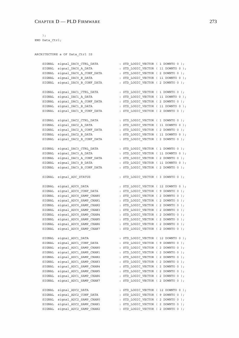
CHAPTER D — PLD FIRMWARE 273
);
END Data_Ctrl;
ARCHITECTURE a OF Data_Ctrl IS
SIGNAL signal_DAC0_CTRL_DATA : STD_LOGIC_VECTOR ( 1 DOWNTO 0 );
SIGNAL signal_DAC0_A_DATA : STD_LOGIC_VECTOR ( 11 DOWNTO 0 );
SIGNAL signal_DAC0_A_CONF_DATA : STD_LOGIC_VECTOR ( 2 DOWNTO 0 );
SIGNAL signal_DAC0_B_DATA : STD_LOGIC_VECTOR ( 11 DOWNTO 0 );
SIGNAL signal_DAC0_B_CONF_DATA : STD_LOGIC_VECTOR ( 2 DOWNTO 0 );
SIGNAL signal_DAC1_CTRL_DATA : STD_LOGIC_VECTOR ( 1 DOWNTO 0 );
SIGNAL signal_DAC1_A_DATA : STD_LOGIC_VECTOR ( 11 DOWNTO 0 );
SIGNAL signal_DAC1_A_CONF_DATA : STD_LOGIC_VECTOR ( 2 DOWNTO 0 );
SIGNAL signal_DAC1_B_DATA : STD_LOGIC_VECTOR ( 11 DOWNTO 0 );
SIGNAL signal_DAC1_B_CONF_DATA : STD_LOGIC_VECTOR ( 2 DOWNTO 0 );
SIGNAL signal_DAC2_CTRL_DATA : STD_LOGIC_VECTOR ( 1 DOWNTO 0 );
SIGNAL signal_DAC2_A_DATA : STD_LOGIC_VECTOR ( 11 DOWNTO 0 );
SIGNAL signal_DAC2_A_CONF_DATA : STD_LOGIC_VECTOR ( 2 DOWNTO 0 );
SIGNAL signal_DAC2_B_DATA : STD_LOGIC_VECTOR ( 11 DOWNTO 0 );
SIGNAL signal_DAC2_B_CONF_DATA : STD_LOGIC_VECTOR ( 2 DOWNTO 0 );
SIGNAL signal_DAC3_CTRL_DATA : STD_LOGIC_VECTOR ( 1 DOWNTO 0 );
SIGNAL signal_DAC3_A_DATA : STD_LOGIC_VECTOR ( 11 DOWNTO 0 );
SIGNAL signal_DAC3_A_CONF_DATA : STD_LOGIC_VECTOR ( 2 DOWNTO 0 );
SIGNAL signal_DAC3_B_DATA : STD_LOGIC_VECTOR ( 11 DOWNTO 0 );
SIGNAL signal_DAC3_B_CONF_DATA : STD_LOGIC_VECTOR ( 2 DOWNTO 0 );
SIGNAL signal_ADC_STATUS : STD_LOGIC_VECTOR ( 3 DOWNTO 0 );
SIGNAL signal_ADC0_DATA : STD_LOGIC_VECTOR ( 12 DOWNTO 0 );
SIGNAL signal_ADC0_CONF_DATA : STD_LOGIC_VECTOR ( 9 DOWNTO 0 );
SIGNAL signal_ADC0_SAMP_CHAN0 : STD_LOGIC_VECTOR ( 2 DOWNTO 0 );
SIGNAL signal_ADC0_SAMP_CHAN1 : STD_LOGIC_VECTOR ( 2 DOWNTO 0 );
SIGNAL signal_ADC0_SAMP_CHAN2 : STD_LOGIC_VECTOR ( 2 DOWNTO 0 );
SIGNAL signal_ADC0_SAMP_CHAN3 : STD_LOGIC_VECTOR ( 2 DOWNTO 0 );
SIGNAL signal_ADC0_SAMP_CHAN4 : STD_LOGIC_VECTOR ( 2 DOWNTO 0 );
SIGNAL signal_ADC0_SAMP_CHAN5 : STD_LOGIC_VECTOR ( 2 DOWNTO 0 );
SIGNAL signal_ADC0_SAMP_CHAN6 : STD_LOGIC_VECTOR ( 2 DOWNTO 0 );
SIGNAL signal_ADC0_SAMP_CHAN7 : STD_LOGIC_VECTOR ( 2 DOWNTO 0 );
SIGNAL signal_ADC1_DATA : STD_LOGIC_VECTOR ( 12 DOWNTO 0 );
SIGNAL signal_ADC1_CONF_DATA : STD_LOGIC_VECTOR ( 9 DOWNTO 0 );
SIGNAL signal_ADC1_SAMP_CHAN0 : STD_LOGIC_VECTOR ( 2 DOWNTO 0 );
SIGNAL signal_ADC1_SAMP_CHAN1 : STD_LOGIC_VECTOR ( 2 DOWNTO 0 );
SIGNAL signal_ADC1_SAMP_CHAN2 : STD_LOGIC_VECTOR ( 2 DOWNTO 0 );
SIGNAL signal_ADC1_SAMP_CHAN3 : STD_LOGIC_VECTOR ( 2 DOWNTO 0 );
SIGNAL signal_ADC1_SAMP_CHAN4 : STD_LOGIC_VECTOR ( 2 DOWNTO 0 );
SIGNAL signal_ADC1_SAMP_CHAN5 : STD_LOGIC_VECTOR ( 2 DOWNTO 0 );
SIGNAL signal_ADC1_SAMP_CHAN6 : STD_LOGIC_VECTOR ( 2 DOWNTO 0 );
SIGNAL signal_ADC1_SAMP_CHAN7 : STD_LOGIC_VECTOR ( 2 DOWNTO 0 );
SIGNAL signal_ADC2_DATA : STD_LOGIC_VECTOR ( 12 DOWNTO 0 );
SIGNAL signal_ADC2_CONF_DATA : STD_LOGIC_VECTOR ( 9 DOWNTO 0 );
SIGNAL signal_ADC2_SAMP_CHAN0 : STD_LOGIC_VECTOR ( 2 DOWNTO 0 );
SIGNAL signal_ADC2_SAMP_CHAN1 : STD_LOGIC_VECTOR ( 2 DOWNTO 0 );
SIGNAL signal_ADC2_SAMP_CHAN2 : STD_LOGIC_VECTOR ( 2 DOWNTO 0 );

CHAPTER D — PLD FIRMWARE 274
SIGNAL signal_ADC2_SAMP_CHAN3 : STD_LOGIC_VECTOR ( 2 DOWNTO 0 );
SIGNAL signal_ADC2_SAMP_CHAN4 : STD_LOGIC_VECTOR ( 2 DOWNTO 0 );
SIGNAL signal_ADC2_SAMP_CHAN5 : STD_LOGIC_VECTOR ( 2 DOWNTO 0 );
SIGNAL signal_ADC2_SAMP_CHAN6 : STD_LOGIC_VECTOR ( 2 DOWNTO 0 );
SIGNAL signal_ADC2_SAMP_CHAN7 : STD_LOGIC_VECTOR ( 2 DOWNTO 0 );
SIGNAL signal_ADC3_DATA : STD_LOGIC_VECTOR ( 12 DOWNTO 0 );
SIGNAL signal_ADC3_CONF_DATA : STD_LOGIC_VECTOR ( 9 DOWNTO 0 );
SIGNAL signal_ADC3_SAMP_CHAN0 : STD_LOGIC_VECTOR ( 2 DOWNTO 0 );
SIGNAL signal_ADC3_SAMP_CHAN1 : STD_LOGIC_VECTOR ( 2 DOWNTO 0 );
SIGNAL signal_ADC3_SAMP_CHAN2 : STD_LOGIC_VECTOR ( 2 DOWNTO 0 );
SIGNAL signal_ADC3_SAMP_CHAN3 : STD_LOGIC_VECTOR ( 2 DOWNTO 0 );
SIGNAL signal_ADC3_SAMP_CHAN4 : STD_LOGIC_VECTOR ( 2 DOWNTO 0 );
SIGNAL signal_ADC3_SAMP_CHAN5 : STD_LOGIC_VECTOR ( 2 DOWNTO 0 );
SIGNAL signal_ADC3_SAMP_CHAN6 : STD_LOGIC_VECTOR ( 2 DOWNTO 0 );
SIGNAL signal_ADC3_SAMP_CHAN7 : STD_LOGIC_VECTOR ( 2 DOWNTO 0 );
SIGNAL signal_LCD_MODE_DATA : STD_LOGIC_VECTOR ( 7 DOWNTO 0 );
SIGNAL signal_LCD_CHAR : STD_LOGIC_VECTOR ( 7 DOWNTO 0 );
SIGNAL signal_LCD_ADDR : STD_LOGIC_VECTOR ( 6 DOWNTO 0 );
SIGNAL signal_LCD_STATUS : STD_LOGIC;
SIGNAL signal_KEYVAL : STD_LOGIC_VECTOR ( 3 DOWNTO 0 );
SIGNAL signal_PWM_STATUS : STD_LOGIC_VECTOR ( 7 DOWNTO 0 );
SIGNAL signal_PWM0_REFA : STD_LOGIC_VECTOR ( 9 DOWNTO 0 );
SIGNAL signal_PWM0_REFB : STD_LOGIC_VECTOR ( 9 DOWNTO 0 );
SIGNAL signal_PWM0_REFC : STD_LOGIC_VECTOR ( 9 DOWNTO 0 );
SIGNAL signal_PWM0_REFN : STD_LOGIC_VECTOR ( 9 DOWNTO 0 );
SIGNAL signal_PWM0_TRIMAX : STD_LOGIC_VECTOR ( 9 DOWNTO 0 );
SIGNAL signal_PWM0_FREQSCALE : STD_LOGIC_VECTOR ( 9 DOWNTO 0 );
SIGNAL signal_PWM0_DEADTIME : STD_LOGIC_VECTOR ( 9 DOWNTO 0 );
SIGNAL signal_PWM0_COMPUPVAL : STD_LOGIC_VECTOR ( 9 DOWNTO 0 );
SIGNAL signal_PWM0_COMPDOWNVAL : STD_LOGIC_VECTOR ( 9 DOWNTO 0 );
SIGNAL signal_PWM1_REFA : STD_LOGIC_VECTOR ( 9 DOWNTO 0 );
SIGNAL signal_PWM1_REFB : STD_LOGIC_VECTOR ( 9 DOWNTO 0 );
SIGNAL signal_PWM1_REFC : STD_LOGIC_VECTOR ( 9 DOWNTO 0 );
SIGNAL signal_PWM1_REFN : STD_LOGIC_VECTOR ( 9 DOWNTO 0 );
SIGNAL signal_PWM1_TRIMAX : STD_LOGIC_VECTOR ( 9 DOWNTO 0 );
SIGNAL signal_PWM1_FREQSCALE : STD_LOGIC_VECTOR ( 9 DOWNTO 0 );
SIGNAL signal_PWM1_DEADTIME : STD_LOGIC_VECTOR ( 9 DOWNTO 0 );
SIGNAL signal_PWM1_COMPUPVAL : STD_LOGIC_VECTOR ( 9 DOWNTO 0 );
SIGNAL signal_PWM1_COMPDOWNVAL : STD_LOGIC_VECTOR ( 9 DOWNTO 0 );
SIGNAL signal_PWM_ERR_TOP : STD_LOGIC_VECTOR ( 8 DOWNTO 0 );
SIGNAL signal_PWM_ERR_BOT : STD_LOGIC_VECTOR ( 8 DOWNTO 0 );
SIGNAL signal_INT_EN : STD_LOGIC_VECTOR ( 14 DOWNTO 0 );
SIGNAL signal_CMD_REG0 : STD_LOGIC_VECTOR ( 6 DOWNTO 0 );
SIGNAL signal_CMD_REG1 : STD_LOGIC_VECTOR ( 5 DOWNTO 0 );
SIGNAL signal_DATA_OUT : STD_LOGIC_VECTOR ( 15 DOWNTO 0 );
SIGNAL signal_DATA_IN : STD_LOGIC_VECTOR ( 15 DOWNTO 0 );
SIGNAL signal_RnW : STD_LOGIC;
SIGNAL signal_INT_REG : STD_LOGIC_VECTOR ( 5 DOWNTO 0 );

CHAPTER D — PLD FIRMWARE 275
COMPONENT Bidir
GENERIC (
n : INTEGER RANGE 0 TO 31 := 15
);
PORT (
BIDIR : INOUT STD_LOGIC_VECTOR ( n DOWNTO 0 );
RnW : IN STD_LOGIC;
CLK : IN STD_LOGIC;
IN_DATA : IN STD_LOGIC_VECTOR ( n DOWNTO 0 );
OUT_DATA : OUT STD_LOGIC_VECTOR ( n DOWNTO 0 )
);
END COMPONENT;
COMPONENT mybuf
GENERIC (
n : INTEGER RANGE 0 TO 15 := 15
);
PORT (
RESET : IN STD_LOGIC;
SEL : IN STD_LOGIC;
IN_DATA : IN STD_LOGIC_VECTOR ( n DOWNTO 0 );
OUT_DATA : OUT STD_LOGIC_VECTOR ( n DOWNTO 0 )
);
END COMPONENT mybuf;
BEGIN
DAC0_CTRL_DATA <= signal_DAC0_CTRL_DATA;
DAC0_A_DATA <= signal_DAC0_A_DATA;
DAC0_A_CONF_DATA <= signal_DAC0_A_CONF_DATA;
DAC0_B_DATA <= signal_DAC0_B_DATA;
DAC0_B_CONF_DATA <= signal_DAC0_B_CONF_DATA;
DAC1_CTRL_DATA <= signal_DAC1_CTRL_DATA;
DAC1_A_DATA <= signal_DAC1_A_DATA;
DAC1_A_CONF_DATA <= signal_DAC1_A_CONF_DATA;
DAC1_B_DATA <= signal_DAC1_B_DATA;
DAC1_B_CONF_DATA <= signal_DAC1_B_CONF_DATA;
DAC2_CTRL_DATA <= signal_DAC2_CTRL_DATA;
DAC2_A_DATA <= signal_DAC2_A_DATA;
DAC2_A_CONF_DATA <= signal_DAC2_A_CONF_DATA;
DAC2_B_DATA <= signal_DAC2_B_DATA;
DAC2_B_CONF_DATA <= signal_DAC2_B_CONF_DATA;
DAC3_CTRL_DATA <= signal_DAC3_CTRL_DATA;
DAC3_A_DATA <= signal_DAC3_A_DATA;
DAC3_A_CONF_DATA <= signal_DAC3_A_CONF_DATA;
DAC3_B_DATA <= signal_DAC3_B_DATA;
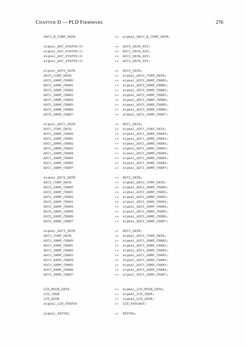
CHAPTER D — PLD FIRMWARE 276
DAC3_B_CONF_DATA <= signal_DAC3_B_CONF_DATA;
signal_ADC_STATUS(0) <= ADC0_DATA_RDY;
signal_ADC_STATUS(1) <= ADC1_DATA_RDY;
signal_ADC_STATUS(2) <= ADC2_DATA_RDY;
signal_ADC_STATUS(3) <= ADC3_DATA_RDY;
signal_ADC0_DATA <= ADC0_DATA;
ADC0_CONF_DATA <= signal_ADC0_CONF_DATA;
ADC0_SAMP_CHAN0 <= signal_ADC0_SAMP_CHAN0;
ADC0_SAMP_CHAN1 <= signal_ADC0_SAMP_CHAN1;
ADC0_SAMP_CHAN2 <= signal_ADC0_SAMP_CHAN2;
ADC0_SAMP_CHAN3 <= signal_ADC0_SAMP_CHAN3;
ADC0_SAMP_CHAN4 <= signal_ADC0_SAMP_CHAN4;
ADC0_SAMP_CHAN5 <= signal_ADC0_SAMP_CHAN5;
ADC0_SAMP_CHAN6 <= signal_ADC0_SAMP_CHAN6;
ADC0_SAMP_CHAN7 <= signal_ADC0_SAMP_CHAN7;
signal_ADC1_DATA <= ADC1_DATA;
ADC1_CONF_DATA <= signal_ADC1_CONF_DATA;
ADC1_SAMP_CHAN0 <= signal_ADC1_SAMP_CHAN0;
ADC1_SAMP_CHAN1 <= signal_ADC1_SAMP_CHAN1;
ADC1_SAMP_CHAN2 <= signal_ADC1_SAMP_CHAN2;
ADC1_SAMP_CHAN3 <= signal_ADC1_SAMP_CHAN3;
ADC1_SAMP_CHAN4 <= signal_ADC1_SAMP_CHAN4;
ADC1_SAMP_CHAN5 <= signal_ADC1_SAMP_CHAN5;
ADC1_SAMP_CHAN6 <= signal_ADC1_SAMP_CHAN6;
ADC1_SAMP_CHAN7 <= signal_ADC1_SAMP_CHAN7;
signal_ADC2_DATA <= ADC2_DATA;
ADC2_CONF_DATA <= signal_ADC2_CONF_DATA;
ADC2_SAMP_CHAN0 <= signal_ADC2_SAMP_CHAN0;
ADC2_SAMP_CHAN1 <= signal_ADC2_SAMP_CHAN1;
ADC2_SAMP_CHAN2 <= signal_ADC2_SAMP_CHAN2;
ADC2_SAMP_CHAN3 <= signal_ADC2_SAMP_CHAN3;
ADC2_SAMP_CHAN4 <= signal_ADC2_SAMP_CHAN4;
ADC2_SAMP_CHAN5 <= signal_ADC2_SAMP_CHAN5;
ADC2_SAMP_CHAN6 <= signal_ADC2_SAMP_CHAN6;
ADC2_SAMP_CHAN7 <= signal_ADC2_SAMP_CHAN7;
signal_ADC3_DATA <= ADC3_DATA;
ADC3_CONF_DATA <= signal_ADC3_CONF_DATA;
ADC3_SAMP_CHAN0 <= signal_ADC3_SAMP_CHAN0;
ADC3_SAMP_CHAN1 <= signal_ADC3_SAMP_CHAN1;
ADC3_SAMP_CHAN2 <= signal_ADC3_SAMP_CHAN2;
ADC3_SAMP_CHAN3 <= signal_ADC3_SAMP_CHAN3;
ADC3_SAMP_CHAN4 <= signal_ADC3_SAMP_CHAN4;
ADC3_SAMP_CHAN5 <= signal_ADC3_SAMP_CHAN5;
ADC3_SAMP_CHAN6 <= signal_ADC3_SAMP_CHAN6;
ADC3_SAMP_CHAN7 <= signal_ADC3_SAMP_CHAN7;
LCD_MODE_DATA <= signal_LCD_MODE_DATA;
LCD_CHAR <= signal_LCD_CHAR;
LCD_ADDR <= signal_LCD_ADDR;
signal_LCD_STATUS <= LCD_RDYnBSY;
signal_KEYVAL <= KEYVAL;

CHAPTER D — PLD FIRMWARE 277
signal_PWM_STATUS(0) <= PWM0_COMPUP;
signal_PWM_STATUS(1) <= PWM0_COMPDOWN;
signal_PWM_STATUS(2) <= PWM0_RAMPDIR;
signal_PWM_STATUS(3) <= PWM0_COUNTERZERO;
signal_PWM_STATUS(4) <= PWM1_COMPUP;
signal_PWM_STATUS(5) <= PWM1_COMPDOWN;
signal_PWM_STATUS(6) <= PWM1_RAMPDIR;
signal_PWM_STATUS(7) <= PWM1_COUNTERZERO;
PWM0_REFA <= signal_PWM0_REFA;
PWM0_REFB <= signal_PWM0_REFB;
PWM0_REFC <= signal_PWM0_REFC;
PWM0_REFN <= signal_PWM0_REFN;
PWM0_TRIMAX <= signal_PWM0_TRIMAX;
PWM0_FREQSCALE <= signal_PWM0_FREQSCALE;
PWM0_DEADTIME <= signal_PWM0_DEADTIME;
PWM0_COMPUPVAL <= signal_PWM0_COMPUPVAL;
PWM0_COMPDOWNVAL <= signal_PWM0_COMPDOWNVAL;
PWM1_REFA <= signal_PWM1_REFA;
PWM1_REFB <= signal_PWM1_REFB;
PWM1_REFC <= signal_PWM1_REFC;
PWM1_REFN <= signal_PWM1_REFN;
PWM1_TRIMAX <= signal_PWM1_TRIMAX;
PWM1_FREQSCALE <= signal_PWM1_FREQSCALE;
PWM1_DEADTIME <= signal_PWM1_DEADTIME;
PWM1_COMPUPVAL <= signal_PWM1_COMPUPVAL;
PWM1_COMPDOWNVAL <= signal_PWM1_COMPDOWNVAL;
signal_PWM_ERR_TOP <= PWM_ERR_TOP;
signal_PWM_ERR_BOT <= PWM_ERR_BOT;
INT_EN <= signal_INT_EN;
signal_INT_REG <= INT_REG;
CMD_REG0 <= signal_CMD_REG0;
CMD_REG1 <= signal_CMD_REG1;
------------------------------------------------------------------------------------------
------------------------------------------------------------------------------------------
dac0_ctrl_map:
MyBuf GENERIC MAP ( n => 1 )
PORT MAP ( RESET => RESET, SEL => DAC0_CTRL_EN,
IN_DATA => signal_DATA_IN ( 1 DOWNTO 0 ),
OUT_DATA => signal_DAC0_CTRL_DATA );
dac0_a_conf_map:
MyBuf GENERIC MAP ( n => 2 )
PORT MAP ( RESET => RESET, SEL => DAC0_A_CONF_EN,
IN_DATA => signal_DATA_IN ( 2 DOWNTO 0 ),
OUT_DATA => signal_DAC0_A_CONF_DATA );
dac0_a_data_map:
MyBuf GENERIC MAP ( n => 11 )
PORT MAP ( RESET => RESET, SEL => DAC0_A_DATA_EN,
IN_DATA => signal_DATA_IN ( 11 DOWNTO 0 ),
OUT_DATA => signal_DAC0_A_DATA );

CHAPTER D — PLD FIRMWARE 278
dac0_b_conf_map:
MyBuf GENERIC MAP ( n => 2 )
PORT MAP ( RESET => RESET, SEL => DAC0_B_CONF_EN,
IN_DATA => signal_DATA_IN ( 2 DOWNTO 0 ),
OUT_DATA => signal_DAC0_B_CONF_DATA );
dac0_b_data_map:
MyBuf GENERIC MAP ( n => 11 )
PORT MAP ( RESET => RESET, SEL => DAC0_B_DATA_EN,
IN_DATA => signal_DATA_IN ( 11 DOWNTO 0 ),
OUT_DATA => signal_DAC0_B_DATA );
------------------------------------------------------------------------------------------
dac1_ctrl_map:
MyBuf GENERIC MAP ( n => 1 )
PORT MAP ( RESET => RESET, SEL => DAC1_CTRL_EN,
IN_DATA => signal_DATA_IN ( 1 DOWNTO 0 ),
OUT_DATA => signal_DAC1_CTRL_DATA );
dac1_a_conf_map:
MyBuf GENERIC MAP ( n => 2 )
PORT MAP ( RESET => RESET, SEL => DAC1_A_CONF_EN,
IN_DATA => signal_DATA_IN ( 2 DOWNTO 0 ),
OUT_DATA => signal_DAC1_A_CONF_DATA );
dac1_a_data_map:
MyBuf GENERIC MAP ( n => 11 )
PORT MAP ( RESET => RESET, SEL => DAC1_A_DATA_EN,
IN_DATA => signal_DATA_IN ( 11 DOWNTO 0 ),
OUT_DATA => signal_DAC1_A_DATA );
dac1_b_conf_map:
MyBuf GENERIC MAP ( n => 2 )
PORT MAP ( RESET => RESET, SEL => DAC1_B_CONF_EN,
IN_DATA => signal_DATA_IN ( 2 DOWNTO 0 ),
OUT_DATA => signal_DAC1_B_CONF_DATA );
dac1_b_data_map:
MyBuf GENERIC MAP ( n => 11 )
PORT MAP ( RESET => RESET, SEL => DAC1_B_DATA_EN,
IN_DATA => signal_DATA_IN ( 11 DOWNTO 0 ),
OUT_DATA => signal_DAC1_B_DATA );
------------------------------------------------------------------------------------------
dac2_ctrl_map:
MyBuf GENERIC MAP ( n => 1 )
PORT MAP ( RESET => RESET, SEL => DAC2_CTRL_EN,
IN_DATA => signal_DATA_IN ( 1 DOWNTO 0 ),
OUT_DATA => signal_DAC2_CTRL_DATA );
dac2_a_conf_map:
MyBuf GENERIC MAP ( n => 2 )
PORT MAP ( RESET => RESET, SEL => DAC2_A_CONF_EN,
IN_DATA => signal_DATA_IN ( 2 DOWNTO 0 ),
OUT_DATA => signal_DAC2_A_CONF_DATA );

CHAPTER D — PLD FIRMWARE 279
dac2_a_data_map:
MyBuf GENERIC MAP ( n => 11 )
PORT MAP ( RESET => RESET, SEL => DAC2_A_DATA_EN,
IN_DATA => signal_DATA_IN ( 11 DOWNTO 0 ),
OUT_DATA => signal_DAC2_A_DATA );
dac2_b_conf_map:
MyBuf GENERIC MAP ( n => 2 )
PORT MAP ( RESET => RESET, SEL => DAC2_B_CONF_EN,
IN_DATA => signal_DATA_IN ( 2 DOWNTO 0 ),
OUT_DATA => signal_DAC2_B_CONF_DATA );
dac2_b_data_map:
MyBuf GENERIC MAP ( n => 11 )
PORT MAP ( RESET => RESET, SEL => DAC2_B_DATA_EN,
IN_DATA => signal_DATA_IN ( 11 DOWNTO 0 ),
OUT_DATA => signal_DAC2_B_DATA );
------------------------------------------------------------------------------------------
dac3_ctrl_map:
MyBuf GENERIC MAP ( n => 1 )
PORT MAP ( RESET => RESET, SEL => DAC3_CTRL_EN,
IN_DATA => signal_DATA_IN ( 1 DOWNTO 0 ),
OUT_DATA => signal_DAC3_CTRL_DATA );
dac3_a_conf_map:
MyBuf GENERIC MAP ( n => 2 )
PORT MAP ( RESET => RESET, SEL => DAC3_A_CONF_EN,
IN_DATA => signal_DATA_IN ( 2 DOWNTO 0 ),
OUT_DATA => signal_DAC3_A_CONF_DATA );
dac3_a_data_map:
MyBuf GENERIC MAP ( n => 11 )
PORT MAP ( RESET => RESET, SEL => DAC3_A_DATA_EN,
IN_DATA => signal_DATA_IN ( 11 DOWNTO 0 ),
OUT_DATA => signal_DAC3_A_DATA );
dac3_b_conf_map:
MyBuf GENERIC MAP ( n => 2 )
PORT MAP ( RESET => RESET, SEL => DAC3_B_CONF_EN,
IN_DATA => signal_DATA_IN ( 2 DOWNTO 0 ),
OUT_DATA => signal_DAC3_B_CONF_DATA );
dac3_b_data_map:
MyBuf GENERIC MAP ( n => 11 )
PORT MAP ( RESET => RESET, SEL => DAC3_B_DATA_EN,
IN_DATA => signal_DATA_IN ( 11 DOWNTO 0 ),
OUT_DATA => signal_DAC3_B_DATA );
------------------------------------------------------------------------------------------
------------------------------------------------------------------------------------------
adc0_conf_map:
MyBuf GENERIC MAP ( n => 9 )
PORT MAP ( RESET => RESET, SEL => ADC0_CONF_EN,
IN_DATA => signal_DATA_IN ( 9 DOWNTO 0 ),
OUT_DATA => signal_ADC0_CONF_DATA );
adc0_samp_chan0_map:

CHAPTER D — PLD FIRMWARE 280
MyBuf GENERIC MAP ( n => 2 )
PORT MAP ( RESET => RESET, SEL => ADC0_SAMP_CHAN0_EN,
IN_DATA => signal_DATA_IN ( 2 DOWNTO 0 ),
OUT_DATA => signal_ADC0_SAMP_CHAN0 );
adc0_samp_chan1_map:
MyBuf GENERIC MAP ( n => 2 )
PORT MAP ( RESET => RESET, SEL => ADC0_SAMP_CHAN1_EN,
IN_DATA => signal_DATA_IN ( 2 DOWNTO 0 ),
OUT_DATA => signal_ADC0_SAMP_CHAN1 );
adc0_samp_chan2_map:
MyBuf GENERIC MAP ( n => 2 )
PORT MAP ( RESET => RESET, SEL => ADC0_SAMP_CHAN2_EN,
IN_DATA => signal_DATA_IN ( 2 DOWNTO 0 ),
OUT_DATA => signal_ADC0_SAMP_CHAN2 );
adc0_samp_chan3_map:
MyBuf GENERIC MAP ( n => 2 )
PORT MAP ( RESET => RESET, SEL => ADC0_SAMP_CHAN3_EN,
IN_DATA => signal_DATA_IN ( 2 DOWNTO 0 ),
OUT_DATA => signal_ADC0_SAMP_CHAN3 );
adc0_samp_chan4_map:
MyBuf GENERIC MAP ( n => 2 )
PORT MAP ( RESET => RESET, SEL => ADC0_SAMP_CHAN4_EN,
IN_DATA => signal_DATA_IN ( 2 DOWNTO 0 ),
OUT_DATA => signal_ADC0_SAMP_CHAN4 );
adc0_samp_chan5_map:
MyBuf GENERIC MAP ( n => 2 )
PORT MAP ( RESET => RESET, SEL => ADC0_SAMP_CHAN5_EN,
IN_DATA => signal_DATA_IN ( 2 DOWNTO 0 ),
OUT_DATA => signal_ADC0_SAMP_CHAN5 );
adc0_samp_chan6_map:
MyBuf GENERIC MAP ( n => 2 )
PORT MAP ( RESET => RESET, SEL => ADC0_SAMP_CHAN6_EN,
IN_DATA => signal_DATA_IN ( 2 DOWNTO 0 ),
OUT_DATA => signal_ADC0_SAMP_CHAN6 );
adc0_samp_chan7_map:
MyBuf GENERIC MAP ( n => 2 )
PORT MAP ( RESET => RESET, SEL => ADC0_SAMP_CHAN7_EN,
IN_DATA => signal_DATA_IN ( 2 DOWNTO 0 ),
OUT_DATA => signal_ADC0_SAMP_CHAN7 );
------------------------------------------------------------------------------------------
adc1_conf_map:
MyBuf GENERIC MAP ( n => 9 )
PORT MAP ( RESET => RESET, SEL => ADC1_CONF_EN,
IN_DATA => signal_DATA_IN ( 9 DOWNTO 0 ),
OUT_DATA => signal_ADC1_CONF_DATA );
adc1_samp_chan0_map:
MyBuf GENERIC MAP ( n => 2 )
PORT MAP ( RESET => RESET, SEL => ADC1_SAMP_CHAN0_EN,
IN_DATA => signal_DATA_IN ( 2 DOWNTO 0 ),

CHAPTER D — PLD FIRMWARE 281
OUT_DATA => signal_ADC1_SAMP_CHAN0 );
adc1_samp_chan1_map:
MyBuf GENERIC MAP ( n => 2 )
PORT MAP ( RESET => RESET, SEL => ADC1_SAMP_CHAN1_EN,
IN_DATA => signal_DATA_IN ( 2 DOWNTO 0 ),
OUT_DATA => signal_ADC1_SAMP_CHAN1 );
adc1_samp_chan2_map:
MyBuf GENERIC MAP ( n => 2 )
PORT MAP ( RESET => RESET, SEL => ADC1_SAMP_CHAN2_EN,
IN_DATA => signal_DATA_IN ( 2 DOWNTO 0 ),
OUT_DATA => signal_ADC1_SAMP_CHAN2 );
adc1_samp_chan3_map:
MyBuf GENERIC MAP ( n => 2 )
PORT MAP ( RESET => RESET, SEL => ADC1_SAMP_CHAN3_EN,
IN_DATA => signal_DATA_IN ( 2 DOWNTO 0 ),
OUT_DATA => signal_ADC1_SAMP_CHAN3 );
adc1_samp_chan4_map:
MyBuf GENERIC MAP ( n => 2 )
PORT MAP ( RESET => RESET, SEL => ADC1_SAMP_CHAN4_EN,
IN_DATA => signal_DATA_IN ( 2 DOWNTO 0 ),
OUT_DATA => signal_ADC1_SAMP_CHAN4 );
adc1_samp_chan5_map:
MyBuf GENERIC MAP ( n => 2 )
PORT MAP ( RESET => RESET, SEL => ADC1_SAMP_CHAN5_EN,
IN_DATA => signal_DATA_IN ( 2 DOWNTO 0 ),
OUT_DATA => signal_ADC1_SAMP_CHAN5 );
adc1_samp_chan6_map:
MyBuf GENERIC MAP ( n => 2 )
PORT MAP ( RESET => RESET, SEL => ADC1_SAMP_CHAN6_EN,
IN_DATA => signal_DATA_IN ( 2 DOWNTO 0 ),
OUT_DATA => signal_ADC1_SAMP_CHAN6 );
adc1_samp_chan7_map:
MyBuf GENERIC MAP ( n => 2 )
PORT MAP ( RESET => RESET, SEL => ADC1_SAMP_CHAN7_EN,
IN_DATA => signal_DATA_IN ( 2 DOWNTO 0 ),
OUT_DATA => signal_ADC1_SAMP_CHAN7 );
------------------------------------------------------------------------------------------
adc2_conf_map:
MyBuf GENERIC MAP ( n => 9 )
PORT MAP ( RESET => RESET, SEL => ADC2_CONF_EN,
IN_DATA => signal_DATA_IN ( 9 DOWNTO 0 ),
OUT_DATA => signal_ADC2_CONF_DATA );
adc2_samp_chan0_map:
MyBuf GENERIC MAP ( n => 2 )
PORT MAP ( RESET => RESET, SEL => ADC2_SAMP_CHAN0_EN,
IN_DATA => signal_DATA_IN ( 2 DOWNTO 0 ),
OUT_DATA => signal_ADC2_SAMP_CHAN0 );
adc2_samp_chan1_map:

CHAPTER D — PLD FIRMWARE 282
MyBuf GENERIC MAP ( n => 2 )
PORT MAP ( RESET => RESET, SEL => ADC2_SAMP_CHAN1_EN,
IN_DATA => signal_DATA_IN ( 2 DOWNTO 0 ),
OUT_DATA => signal_ADC2_SAMP_CHAN1 );
adc2_samp_chan2_map:
MyBuf GENERIC MAP ( n => 2 )
PORT MAP ( RESET => RESET, SEL => ADC2_SAMP_CHAN2_EN,
IN_DATA => signal_DATA_IN ( 2 DOWNTO 0 ),
OUT_DATA => signal_ADC2_SAMP_CHAN2 );
adc2_samp_chan3_map:
MyBuf GENERIC MAP ( n => 2 )
PORT MAP ( RESET => RESET, SEL => ADC2_SAMP_CHAN3_EN,
IN_DATA => signal_DATA_IN ( 2 DOWNTO 0 ),
OUT_DATA => signal_ADC2_SAMP_CHAN3 );
adc2_samp_chan4_map:
MyBuf GENERIC MAP ( n => 2 )
PORT MAP ( RESET => RESET, SEL => ADC2_SAMP_CHAN4_EN,
IN_DATA => signal_DATA_IN ( 2 DOWNTO 0 ),
OUT_DATA => signal_ADC2_SAMP_CHAN4 );
adc2_samp_chan5_map:
MyBuf GENERIC MAP ( n => 2 )
PORT MAP ( RESET => RESET, SEL => ADC2_SAMP_CHAN5_EN,
IN_DATA => signal_DATA_IN ( 2 DOWNTO 0 ),
OUT_DATA => signal_ADC2_SAMP_CHAN5 );
adc2_samp_chan6_map:
MyBuf GENERIC MAP ( n => 2 )
PORT MAP ( RESET => RESET, SEL => ADC2_SAMP_CHAN6_EN,
IN_DATA => signal_DATA_IN ( 2 DOWNTO 0 ),
OUT_DATA => signal_ADC2_SAMP_CHAN6 );
adc2_samp_chan7_map:
MyBuf GENERIC MAP ( n => 2 )
PORT MAP ( RESET => RESET, SEL => ADC2_SAMP_CHAN7_EN,
IN_DATA => signal_DATA_IN ( 2 DOWNTO 0 ),
OUT_DATA => signal_ADC2_SAMP_CHAN7 );
------------------------------------------------------------------------------------------
adc3_conf_map:
MyBuf GENERIC MAP ( n => 9 )
PORT MAP ( RESET => RESET, SEL => ADC3_CONF_EN,
IN_DATA => signal_DATA_IN ( 9 DOWNTO 0 ),
OUT_DATA => signal_ADC3_CONF_DATA );
adc3_samp_chan0_map:
MyBuf GENERIC MAP ( n => 2 )
PORT MAP ( RESET => RESET, SEL => ADC3_SAMP_CHAN0_EN,
IN_DATA => signal_DATA_IN ( 2 DOWNTO 0 ),
OUT_DATA => signal_ADC3_SAMP_CHAN0 );
adc3_samp_chan1_map:
MyBuf GENERIC MAP ( n => 2 )
PORT MAP ( RESET => RESET, SEL => ADC3_SAMP_CHAN1_EN,
IN_DATA => signal_DATA_IN ( 2 DOWNTO 0 ),

CHAPTER D — PLD FIRMWARE 283
OUT_DATA => signal_ADC3_SAMP_CHAN1 );
adc3_samp_chan2_map:
MyBuf GENERIC MAP ( n => 2 )
PORT MAP ( RESET => RESET, SEL => ADC3_SAMP_CHAN2_EN,
IN_DATA => signal_DATA_IN ( 2 DOWNTO 0 ),
OUT_DATA => signal_ADC3_SAMP_CHAN2 );
adc3_samp_chan3_map:
MyBuf GENERIC MAP ( n => 2 )
PORT MAP ( RESET => RESET, SEL => ADC3_SAMP_CHAN3_EN,
IN_DATA => signal_DATA_IN ( 2 DOWNTO 0 ),
OUT_DATA => signal_ADC3_SAMP_CHAN3 );
adc3_samp_chan4_map:
MyBuf GENERIC MAP ( n => 2 )
PORT MAP ( RESET => RESET, SEL => ADC3_SAMP_CHAN4_EN,
IN_DATA => signal_DATA_IN ( 2 DOWNTO 0 ),
OUT_DATA => signal_ADC3_SAMP_CHAN4 );
adc3_samp_chan5_map:
MyBuf GENERIC MAP ( n => 2 )
PORT MAP ( RESET => RESET, SEL => ADC3_SAMP_CHAN5_EN,
IN_DATA => signal_DATA_IN ( 2 DOWNTO 0 ),
OUT_DATA => signal_ADC3_SAMP_CHAN5 );
adc3_samp_chan6_map:
MyBuf GENERIC MAP ( n => 2 )
PORT MAP ( RESET => RESET, SEL => ADC3_SAMP_CHAN6_EN,
IN_DATA => signal_DATA_IN ( 2 DOWNTO 0 ),
OUT_DATA => signal_ADC3_SAMP_CHAN6 );
adc3_samp_chan7_map:
MyBuf GENERIC MAP ( n => 2 )
PORT MAP ( RESET => RESET, SEL => ADC3_SAMP_CHAN7_EN,
IN_DATA => signal_DATA_IN ( 2 DOWNTO 0 ),
OUT_DATA => signal_ADC3_SAMP_CHAN7 );
------------------------------------------------------------------------------------------
------------------------------------------------------------------------------------------
lcd_mode_map:
MyBuf GENERIC MAP ( n => 7 )
PORT MAP ( RESET => RESET, SEL => LCD_MODE_EN,
IN_DATA => signal_DATA_IN ( 7 DOWNTO 0 ),
OUT_DATA => signal_LCD_MODE_DATA );
lcd_addr_map:
MyBuf GENERIC MAP ( n => 6 )
PORT MAP ( RESET => RESET, SEL => LCD_ADDR_EN,
IN_DATA => signal_DATA_IN ( 6 DOWNTO 0 ),
OUT_DATA => signal_LCD_ADDR ( 6 DOWNTO 0 ) );
lcd_char_map:
MyBuf GENERIC MAP ( n => 7 )
PORT MAP ( RESET => RESET, SEL => LCD_CHAR_EN,
IN_DATA => signal_DATA_IN ( 7 DOWNTO 0 ),
OUT_DATA => signal_LCD_CHAR ( 7 DOWNTO 0 ) );

CHAPTER D — PLD FIRMWARE 284
------------------------------------------------------------------------------------------
------------------------------------------------------------------------------------------
pwm0_refa_map:
MyBuf GENERIC MAP ( n => 9 )
PORT MAP ( RESET => RESET, SEL => PWM0_REFA_EN,
IN_DATA => signal_DATA_IN ( 9 DOWNTO 0 ),
OUT_DATA => signal_PWM0_REFA );
pwm0_refb_map:
MyBuf GENERIC MAP ( n => 9 )
PORT MAP ( RESET => RESET, SEL => PWM0_REFB_EN,
IN_DATA => signal_DATA_IN ( 9 DOWNTO 0 ),
OUT_DATA => signal_PWM0_REFB );
pwm0_refc_map:
MyBuf GENERIC MAP ( n => 9 )
PORT MAP ( RESET => RESET, SEL => PWM0_REFC_EN,
IN_DATA => signal_DATA_IN ( 9 DOWNTO 0 ),
OUT_DATA => signal_PWM0_REFC );
pwm0_refn_map:
MyBuf GENERIC MAP ( n => 9 )
PORT MAP ( RESET => RESET, SEL => PWM0_REFN_EN,
IN_DATA => signal_DATA_IN ( 9 DOWNTO 0 ),
OUT_DATA => signal_PWM0_REFN );
pwm0_trimax_map:
MyBuf GENERIC MAP ( n => 9 )
PORT MAP ( RESET => RESET, SEL => PWM0_TRIMAX_EN,
IN_DATA => signal_DATA_IN ( 9 DOWNTO 0 ),
OUT_DATA => signal_PWM0_TRIMAX );
pwm0_trifreqscale_map:
MyBuf GENERIC MAP ( n => 9 )
PORT MAP ( RESET => RESET, SEL => PWM0_TRIFREQSCALE_EN,
IN_DATA => signal_DATA_IN ( 9 DOWNTO 0 ),
OUT_DATA => signal_PWM0_FREQSCALE );
pwm0_deadtime_map:
MyBuf GENERIC MAP ( n => 9 )
PORT MAP ( RESET => RESET, SEL => PWM0_DEADTIME_EN,
IN_DATA => signal_DATA_IN ( 9 DOWNTO 0 ),
OUT_DATA => signal_PWM0_DEADTIME );
pwm0_upval_map:
MyBuf GENERIC MAP ( n => 9 )
PORT MAP ( RESET => RESET, SEL => PWM0_UPVAL_EN,
IN_DATA => signal_DATA_IN ( 9 DOWNTO 0 ),
OUT_DATA => signal_PWM0_COMPUPVAL );
pwm0_downval_map:
MyBuf GENERIC MAP ( n => 9 )
PORT MAP ( RESET => RESET, SEL => PWM0_DOWNVAL_EN,
IN_DATA => signal_DATA_IN ( 9 DOWNTO 0 ),
OUT_DATA => signal_PWM0_COMPDOWNVAL );
------------------------------------------------------------------------------------------
CHAPTER D — PLD FIRMWARE 285
pwm1_refa_map:
MyBuf GENERIC MAP ( n => 9 )
PORT MAP ( RESET => RESET, SEL => PWM1_REFA_EN,
IN_DATA => signal_DATA_IN ( 9 DOWNTO 0 ),
OUT_DATA => signal_PWM1_REFA );
pwm1_refb_map:
MyBuf GENERIC MAP ( n => 9 )
PORT MAP ( RESET => RESET, SEL => PWM1_REFB_EN,
IN_DATA => signal_DATA_IN ( 9 DOWNTO 0 ),
OUT_DATA => signal_PWM1_REFB );
pwm1_refc_map:
MyBuf GENERIC MAP ( n => 9 )
PORT MAP ( RESET => RESET, SEL => PWM1_REFC_EN,
IN_DATA => signal_DATA_IN ( 9 DOWNTO 0 ),
OUT_DATA => signal_PWM1_REFC );
pwm1_refn_map:
MyBuf GENERIC MAP ( n => 9 )
PORT MAP ( RESET => RESET, SEL => PWM1_REFN_EN,
IN_DATA => signal_DATA_IN ( 9 DOWNTO 0 ),
OUT_DATA => signal_PWM1_REFN );
pwm1_trimax_map:
MyBuf GENERIC MAP ( n => 9 )
PORT MAP ( RESET => RESET, SEL => PWM1_TRIMAX_EN,
IN_DATA => signal_DATA_IN ( 9 DOWNTO 0 ),
OUT_DATA => signal_PWM1_TRIMAX );
pwm1_trifreqscale_map:
MyBuf GENERIC MAP ( n => 9 )
PORT MAP ( RESET => RESET, SEL => PWM1_TRIFREQSCALE_EN,
IN_DATA => signal_DATA_IN ( 9 DOWNTO 0 ),
OUT_DATA => signal_PWM1_FREQSCALE );
pwm1_deadtime_map:
MyBuf GENERIC MAP ( n => 9 )
PORT MAP ( RESET => RESET, SEL => PWM1_DEADTIME_EN,
IN_DATA => signal_DATA_IN ( 9 DOWNTO 0 ),
OUT_DATA => signal_PWM1_DEADTIME );
pwm1_upval_map:
MyBuf GENERIC MAP ( n => 9 )
PORT MAP ( RESET => RESET, SEL => PWM1_UPVAL_EN,
IN_DATA => signal_DATA_IN ( 9 DOWNTO 0 ),
OUT_DATA => signal_PWM1_COMPUPVAL );
pwm1_downval_map:
MyBuf GENERIC MAP ( n => 9 )
PORT MAP ( RESET => RESET, SEL => PWM1_DOWNVAL_EN,
IN_DATA => signal_DATA_IN ( 9 DOWNTO 0 ),
OUT_DATA => signal_PWM1_COMPDOWNVAL );
------------------------------------------------------------------------------------------
------------------------------------------------------------------------------------------
int_en_map:
MyBuf GENERIC MAP ( n => 14 )
CHAPTER D — PLD FIRMWARE 286
PORT MAP ( RESET => RESET, SEL => INT_EN_EN,
IN_DATA => signal_DATA_IN ( 14 DOWNTO 0 ),
OUT_DATA => signal_INT_EN );
------------------------------------------------------------------------------------------
------------------------------------------------------------------------------------------
cmd_reg0_map:
MyBuf GENERIC MAP ( n => 6 )
PORT MAP ( RESET => RESET, SEL => CMD_REG0_EN,
IN_DATA => signal_DATA_IN ( 6 DOWNTO 0 ),
OUT_DATA => signal_CMD_REG0 );
cmd_reg1_map:
MyBuf GENERIC MAP ( n => 5 )
PORT MAP ( RESET => RESET, SEL => CMD_REG1_EN,
IN_DATA => signal_DATA_IN ( 5 DOWNTO 0 ),
OUT_DATA => signal_CMD_REG1 );
------------------------------------------------------------------------------------------
------------------------------------------------------------------------------------------
bidir_bus_map:
bidir PORT MAP ( BIDIR => DATA, RnW => signal_RnW, CLK => CLK,
IN_DATA => signal_DATA_OUT, OUT_DATA => signal_DATA_IN );
------------------------------------------------------------------------------------------
------------------------------------------------------------------------------------------
signal_RnW
<= ’0’ WHEN ( ADC_STATUS_EN = ’1’ )or( ADC0_DATA_EN = ’1’ )or
( ADC1_DATA_EN = ’1’ )or( ADC2_DATA_EN = ’1’ )or
( ADC3_DATA_EN = ’1’ )or( KEYVAL_EN = ’1’ )or
( PWM_ERR_TOP_EN = ’1’ )or( PWM_ERR_BOT_EN = ’1’ )or
( LCD_STATUS_EN = ’1’ )or( PWM_STATUS_EN = ’1’ )or
( INT_REG_EN = ’1’) ELSE
’1’;
RnW
<= signal_RnW;
signal_DATA_OUT( 0 )
<= signal_ADC_STATUS ( 0 ) WHEN ( ADC_STATUS_EN = ’1’ ) ELSE
signal_ADC0_DATA ( 0 ) WHEN ( ADC0_DATA_EN = ’1’ ) ELSE
signal_ADC1_DATA ( 0 ) WHEN ( ADC1_DATA_EN = ’1’ ) ELSE
signal_ADC2_DATA ( 0 ) WHEN ( ADC2_DATA_EN = ’1’ ) ELSE
signal_ADC3_DATA ( 0 ) WHEN ( ADC3_DATA_EN = ’1’ ) ELSE
signal_LCD_STATUS WHEN ( LCD_STATUS_EN = ’1’ ) ELSE
signal_KEYVAL ( 0 ) WHEN ( KEYVAL_EN = ’1’ ) ELSE
signal_PWM_STATUS ( 0 ) WHEN ( PWM_STATUS_EN = ’1’ ) ELSE
signal_PWM_ERR_TOP ( 0 ) WHEN ( PWM_ERR_TOP_EN = ’1’ ) ELSE
signal_PWM_ERR_BOT ( 0 ) WHEN ( PWM_ERR_BOT_EN = ’1’ ) ELSE
signal_INT_REG ( 0 ) WHEN ( INT_REG_EN = ’1’ ) ELSE
’0’;
signal_DATA_OUT( 3 DOWNTO 1 )
<= signal_ADC_STATUS ( 3 DOWNTO 1 ) WHEN ( ADC_STATUS_EN = ’1’ ) ELSE
signal_ADC0_DATA ( 3 DOWNTO 1 ) WHEN ( ADC0_DATA_EN = ’1’ ) ELSE

CHAPTER D — PLD FIRMWARE 287
signal_ADC1_DATA ( 3 DOWNTO 1 ) WHEN ( ADC1_DATA_EN = ’1’ ) ELSE
signal_ADC2_DATA ( 3 DOWNTO 1 ) WHEN ( ADC2_DATA_EN = ’1’ ) ELSE
signal_ADC3_DATA ( 3 DOWNTO 1 ) WHEN ( ADC3_DATA_EN = ’1’ ) ELSE
signal_KEYVAL ( 3 DOWNTO 1 ) WHEN ( KEYVAL_EN = ’1’ ) ELSE
signal_PWM_STATUS ( 3 DOWNTO 1 ) WHEN ( PWM_STATUS_EN = ’1’ ) ELSE
signal_PWM_ERR_TOP ( 3 DOWNTO 1 ) WHEN ( PWM_ERR_TOP_EN = ’1’ ) ELSE
signal_PWM_ERR_BOT ( 3 DOWNTO 1 ) WHEN ( PWM_ERR_BOT_EN = ’1’ ) ELSE
signal_INT_REG ( 3 DOWNTO 1 ) WHEN ( INT_REG_EN = ’1’ ) ELSE
"000";
signal_DATA_OUT( 5 DOWNTO 4 )
<= signal_ADC0_DATA ( 5 DOWNTO 4 ) WHEN ( ADC0_DATA_EN = ’1’ ) ELSE
signal_ADC1_DATA ( 5 DOWNTO 4 ) WHEN ( ADC1_DATA_EN = ’1’ ) ELSE
signal_ADC2_DATA ( 5 DOWNTO 4 ) WHEN ( ADC2_DATA_EN = ’1’ ) ELSE
signal_ADC3_DATA ( 5 DOWNTO 4 ) WHEN ( ADC3_DATA_EN = ’1’ ) ELSE
signal_PWM_STATUS ( 5 DOWNTO 4 ) WHEN ( PWM_STATUS_EN = ’1’ ) ELSE
signal_PWM_ERR_TOP ( 5 DOWNTO 4 ) WHEN ( PWM_ERR_TOP_EN = ’1’ ) ELSE
signal_PWM_ERR_BOT ( 5 DOWNTO 4 ) WHEN ( PWM_ERR_BOT_EN = ’1’ ) ELSE
signal_INT_REG ( 5 DOWNTO 4 ) WHEN ( INT_REG_EN = ’1’ ) ELSE
"00";
signal_DATA_OUT( 7 DOWNTO 6 )
<= signal_ADC0_DATA ( 7 DOWNTO 6 ) WHEN ( ADC0_DATA_EN = ’1’ ) ELSE
signal_ADC1_DATA ( 7 DOWNTO 6 ) WHEN ( ADC1_DATA_EN = ’1’ ) ELSE
signal_ADC2_DATA ( 7 DOWNTO 6 ) WHEN ( ADC2_DATA_EN = ’1’ ) ELSE
signal_ADC3_DATA ( 7 DOWNTO 6 ) WHEN ( ADC3_DATA_EN = ’1’ ) ELSE
signal_PWM_STATUS ( 7 DOWNTO 6 ) WHEN ( PWM_STATUS_EN = ’1’ ) ELSE
signal_PWM_ERR_TOP ( 7 DOWNTO 6 ) WHEN ( PWM_ERR_TOP_EN = ’1’ ) ELSE
signal_PWM_ERR_BOT ( 7 DOWNTO 6 ) WHEN ( PWM_ERR_BOT_EN = ’1’ ) ELSE
"00";
signal_DATA_OUT( 8 )
<= signal_ADC0_DATA ( 8 ) WHEN ( ADC0_DATA_EN = ’1’ ) ELSE
signal_ADC1_DATA ( 8 ) WHEN ( ADC1_DATA_EN = ’1’ ) ELSE
signal_ADC2_DATA ( 8 ) WHEN ( ADC2_DATA_EN = ’1’ ) ELSE
signal_ADC3_DATA ( 8 ) WHEN ( ADC3_DATA_EN = ’1’ ) ELSE
signal_PWM_ERR_TOP ( 8 ) WHEN ( PWM_ERR_TOP_EN = ’1’ ) ELSE
signal_PWM_ERR_BOT ( 8 ) WHEN ( PWM_ERR_BOT_EN = ’1’ ) ELSE
’0’;
signal_DATA_OUT( 12 DOWNTO 9 )
<= signal_ADC0_DATA ( 12 DOWNTO 9 ) WHEN ( ADC0_DATA_EN = ’1’ ) ELSE
signal_ADC1_DATA ( 12 DOWNTO 9 ) WHEN ( ADC1_DATA_EN = ’1’ ) ELSE
signal_ADC2_DATA ( 12 DOWNTO 9 ) WHEN ( ADC2_DATA_EN = ’1’ ) ELSE
signal_ADC3_DATA ( 12 DOWNTO 9 ) WHEN ( ADC3_DATA_EN = ’1’ ) ELSE
"0000";
signal_DATA_OUT( 15 DOWNTO 13 ) <= "000";
END a;

CHAPTER D — PLD FIRMWARE 288
D.2.6 VHDL Code for the MyBuf Module of FPGA Analog-- PEC33 - Buffer 2002-10-28
LIBRARY ieee;
USE ieee.std_logic_1164.all;
USE ieee.std_logic_arith.all;
-- -------------------------------------------------------
-- | RESET | SEL | IN_DATA | OUT_DATA |
-- -------------------------------------------------------
-- -------------------------------------------------------
-- | 1 | X | XX...X | 00...0 |
-- -------------------------------------------------------
-- | 0 | 1 | Data | IN_DATA |
-- -------------------------------------------------------
-- | 0 | 0 | XX...X | OUT_DATA |
-- -------------------------------------------------------
ENTITY mybuf IS
GENERIC (
n : INTEGER RANGE 0 TO 15 := 15
);
PORT (
RESET : IN STD_LOGIC;
SEL : IN STD_LOGIC;
IN_DATA : IN STD_LOGIC_VECTOR ( n DOWNTO 0 );
OUT_DATA : OUT STD_LOGIC_VECTOR ( n DOWNTO 0 )
);
END mybuf;
ARCHITECTURE a OF mybuf IS
SIGNAL signal_out : STD_LOGIC_VECTOR ( n DOWNTO 0 );
BEGIN
signal_out <= ( OTHERS => ’0’ ) WHEN ( RESET = ’1’ ) ELSE
IN_DATA WHEN ( SEL = ’1’ ) ELSE
signal_out;
OUT_DATA <= signal_out;
END a;
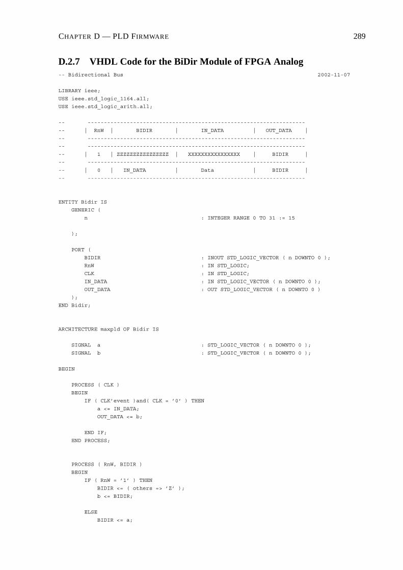
CHAPTER D — PLD FIRMWARE 289
D.2.7 VHDL Code for the BiDir Module of FPGA Analog-- Bidirectional Bus 2002-11-07
LIBRARY ieee;
USE ieee.std_logic_1164.all;
USE ieee.std_logic_arith.all;
-- -------------------------------------------------------------------
-- | RnW | BIDIR | IN_DATA | OUT_DATA |
-- -------------------------------------------------------------------
-- -------------------------------------------------------------------
-- | 1 | ZZZZZZZZZZZZZZZZ | XXXXXXXXXXXXXXXX | BIDIR |
-- -------------------------------------------------------------------
-- | 0 | IN_DATA | Data | BIDIR |
-- -------------------------------------------------------------------
ENTITY Bidir IS
GENERIC (
n : INTEGER RANGE 0 TO 31 := 15
);
PORT (
BIDIR : INOUT STD_LOGIC_VECTOR ( n DOWNTO 0 );
RnW : IN STD_LOGIC;
CLK : IN STD_LOGIC;
IN_DATA : IN STD_LOGIC_VECTOR ( n DOWNTO 0 );
OUT_DATA : OUT STD_LOGIC_VECTOR ( n DOWNTO 0 )
);
END Bidir;
ARCHITECTURE maxpld OF Bidir IS
SIGNAL a : STD_LOGIC_VECTOR ( n DOWNTO 0 );
SIGNAL b : STD_LOGIC_VECTOR ( n DOWNTO 0 );
BEGIN
PROCESS ( CLK )
BEGIN
IF ( CLK’event )and( CLK = ’0’ ) THEN
a <= IN_DATA;
OUT_DATA <= b;
END IF;
END PROCESS;
PROCESS ( RnW, BIDIR )
BEGIN
IF ( RnW = ’1’ ) THEN
BIDIR <= ( others => ’Z’ );
b <= BIDIR;
ELSE
BIDIR <= a;
CHAPTER D — PLD FIRMWARE 290
b <= BIDIR;
END IF;
END PROCESS;
END maxpld;

CHAPTER D — PLD FIRMWARE 291
D.2.8 VHDL Code for the Interrupt Ctrl Module of FPGA Analog-- FPGA Analog - Interrupt Controller 2002-11-07
LIBRARY ieee;
USE ieee.std_logic_1164.all;
USE ieee.std_logic_arith.all;
-- -----------------------------------------------
-- | Interrupt enable register |
-- -----------------------------------------------
-- | Bit No. | Function |
-- -----------------------------------------------
-- -----------------------------------------------
-- | 0 | ADC0 sample ready |
-- -----------------------------------------------
-- | 1 | ADC1 sample ready |
-- -----------------------------------------------
-- | 2 | ADC2 sample ready |
-- -----------------------------------------------
-- | 3 | ADC3 sample ready |
-- -----------------------------------------------
-- | 4 | Keypressed on keypad |
-- -----------------------------------------------
-- | 5 | PWM TOP error |
-- -----------------------------------------------
-- | 6 | PWM BOTTOM error |
-- -----------------------------------------------
-- | 7 | PWM block 0 compare up event |
-- -----------------------------------------------
-- | 8 | PWM block 0 compare down event |
-- -----------------------------------------------
-- | 9 | PWM block 0 ramp direction event |
-- -----------------------------------------------
-- | 10 | PWM block 0 counterzero event |
-- -----------------------------------------------
-- | 11 | PWM block 1 compare up event |
-- -----------------------------------------------
-- | 12 | PWM block 1 compare down event |
-- -----------------------------------------------
-- | 13 | PWM block 1 ramp direction event |
-- -----------------------------------------------
-- | 14 | PWM block 1 counterzero event |
-- -----------------------------------------------
-- -----------------------------------------------
-- | Interrupt register |
-- -----------------------------------------------
-- | Bit No. | Function |
-- -----------------------------------------------
-- -----------------------------------------------
-- | 0 | ADC event |
-- -----------------------------------------------
-- | 1 | Keypad event |
-- -----------------------------------------------
-- | 2 | PWM TOP error |
-- -----------------------------------------------
-- | 3 | PWM BOTTOM error |
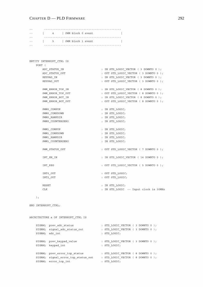
CHAPTER D — PLD FIRMWARE 292
-- -----------------------------------------------
-- | 4 | PWM block 0 event |
-- -----------------------------------------------
-- | 5 | PWM block 1 event |
-- -----------------------------------------------
ENTITY INTERRUPT_CTRL IS
PORT (
ADC_STATUS_IN : IN STD_LOGIC_VECTOR ( 3 DOWNTO 0 );
ADC_STATUS_OUT : OUT STD_LOGIC_VECTOR ( 3 DOWNTO 0 );
KEYPAD_IN : IN STD_LOGIC_VECTOR ( 3 DOWNTO 0 );
KEYPAD_OUT : OUT STD_LOGIC_VECTOR ( 3 DOWNTO 0 );
PWM_ERROR_TOP_IN : IN STD_LOGIC_VECTOR ( 8 DOWNTO 0 );
PWM_ERROR_TOP_OUT : OUT STD_LOGIC_VECTOR ( 8 DOWNTO 0 );
PWM_ERROR_BOT_IN : IN STD_LOGIC_VECTOR ( 8 DOWNTO 0 );
PWM_ERROR_BOT_OUT : OUT STD_LOGIC_VECTOR ( 8 DOWNTO 0 );
PWM0_COMPUP : IN STD_LOGIC;
PWM0_COMPDOWN : IN STD_LOGIC;
PWM0_RAMPDIR : IN STD_LOGIC;
PWM0_COUNTERZERO : IN STD_LOGIC;
PWM1_COMPUP : IN STD_LOGIC;
PWM1_COMPDOWN : IN STD_LOGIC;
PWM1_RAMPDIR : IN STD_LOGIC;
PWM1_COUNTERZERO : IN STD_LOGIC;
PWM_STATUS_OUT : OUT STD_LOGIC_VECTOR ( 7 DOWNTO 0 );
INT_EN_IN : IN STD_LOGIC_VECTOR ( 14 DOWNTO 0 );
INT_REG : OUT STD_LOGIC_VECTOR ( 5 DOWNTO 0 );
INT0_OUT : OUT STD_LOGIC;
INT2_OUT : OUT STD_LOGIC;
RESET : IN STD_LOGIC;
CLK : IN STD_LOGIC -- Input clock is 30MHz
);
END INTERRUPT_CTRL;
ARCHITECTURE a OF INTERRUPT_CTRL IS
SIGNAL prev_adc_status : STD_LOGIC_VECTOR ( 3 DOWNTO 0 );
SIGNAL signal_adc_status_out : STD_LOGIC_VECTOR ( 3 DOWNTO 0 );
SIGNAL adc_int : STD_LOGIC;
SIGNAL prev_keypad_value : STD_LOGIC_VECTOR ( 3 DOWNTO 0 );
SIGNAL keypad_int : STD_LOGIC;
SIGNAL prev_error_top_status : STD_LOGIC_VECTOR ( 8 DOWNTO 0 );
SIGNAL signal_error_top_status_out : STD_LOGIC_VECTOR ( 8 DOWNTO 0 );
SIGNAL error_top_int : STD_LOGIC;

CHAPTER D — PLD FIRMWARE 293
SIGNAL prev_error_bot_status : STD_LOGIC_VECTOR ( 8 DOWNTO 0 );
SIGNAL signal_error_bot_status_out : STD_LOGIC_VECTOR ( 8 DOWNTO 0 );
SIGNAL error_bot_int : STD_LOGIC;
SIGNAL pwm0_status_in : STD_LOGIC_VECTOR ( 3 DOWNTO 0 );
SIGNAL prev_pwm0_status : STD_LOGIC_VECTOR ( 3 DOWNTO 0 );
SIGNAL signal_pwm0_status_out : STD_LOGIC_VECTOR ( 3 DOWNTO 0 );
SIGNAL pwm0_status_int : STD_LOGIC;
SIGNAL pwm1_status_in : STD_LOGIC_VECTOR ( 3 DOWNTO 0 );
SIGNAL prev_pwm1_status : STD_LOGIC_VECTOR ( 3 DOWNTO 0 );
SIGNAL signal_pwm1_status_out : STD_LOGIC_VECTOR ( 3 DOWNTO 0 );
SIGNAL pwm1_status_int : STD_LOGIC;
SIGNAL int0_trig : STD_LOGIC;
SIGNAL int2_trig : STD_LOGIC;
SIGNAL int0_cntr : INTEGER RANGE 0 TO 7;
SIGNAL int2_cntr : INTEGER RANGE 0 TO 7;
SIGNAL signal_INT_REG : STD_LOGIC_VECTOR ( 5 DOWNTO 0 );
SIGNAL signal_prev_INT_REG : STD_LOGIC_VECTOR ( 5 DOWNTO 0 );
BEGIN
int0_trig <= ( adc_int )and( keypad_int )and
( pwm0_status_int )and( pwm1_status_int );
int2_trig <= ( error_top_int )and( error_bot_int );
INT_REG <= signal_INT_REG;
ADC_STATUS_OUT <= not signal_adc_status_out;
signal_INT_REG( 0 ) <= ’0’ WHEN ( INT_EN_IN( 3 DOWNTO 0 ) = "0000" ) ELSE
’1’ WHEN ( signal_adc_status_out /= "1111" ) ELSE
’0’;
KEYPAD_OUT <= prev_keypad_value;
PWM_ERROR_TOP_OUT <= not signal_error_top_status_out;
PWM_ERROR_BOT_OUT <= not signal_error_bot_status_out;
pwm0_status_in( 0 ) <= PWM0_COMPUP;
pwm0_status_in( 1 ) <= PWM0_COMPDOWN;
pwm0_status_in( 2 ) <= PWM0_RAMPDIR;
pwm0_status_in( 3 ) <= PWM0_COUNTERZERO;
pwm1_status_in( 0 ) <= PWM1_COMPUP;
pwm1_status_in( 1 ) <= PWM1_COMPDOWN;
pwm1_status_in( 2 ) <= PWM1_RAMPDIR;
pwm1_status_in( 3 ) <= PWM1_COUNTERZERO;
PWM_STATUS_OUT ( 3 DOWNTO 0 )
<= signal_pwm0_status_out;
signal_INT_REG( 4 ) <= ’0’ WHEN ( INT_EN_IN( 10 DOWNTO 7 ) = "0000" ) ELSE
’1’ WHEN ( signal_pwm0_status_out /= "0000" ) ELSE
’0’;
PWM_STATUS_OUT ( 7 DOWNTO 4 )

CHAPTER D — PLD FIRMWARE 294
<= signal_pwm1_status_out;
signal_INT_REG( 5 ) <= ’0’ WHEN ( INT_EN_IN( 14 DOWNTO 11 ) = "0000" ) ELSE
’1’ WHEN ( signal_pwm1_status_out /= "0000" ) ELSE
’0’;
------------------------------------------------------------------------------------------
int0_proc:
PROCESS ( CLK, int0_trig )
BEGIN
IF ( int0_trig = ’0’ ) THEN
INT0_OUT <= ’1’;
int0_cntr <= 0;
ELSIF ( CLK’event )and( CLK = ’1’ ) THEN
IF ( RESET = ’1’ )or( int0_cntr = 7 ) THEN
int0_cntr <= 7;
INT0_OUT <= ’1’;
ELSE
int0_cntr <= int0_cntr+1;
INT0_OUT <= ’0’;
END IF;
END IF;
END PROCESS int0_proc;
------------------------------------------------------------------------------------------
int2_proc:
PROCESS ( CLK, int2_trig )
BEGIN
IF ( int2_trig = ’0’ ) THEN
INT2_OUT <= ’1’;
int2_cntr <= 0;
ELSIF ( CLK’event )and( CLK = ’1’ ) THEN
IF ( RESET = ’1’ )or( int2_cntr = 7 ) THEN
int2_cntr <= 7;
INT2_OUT <= ’1’;
ELSE
int2_cntr <= int2_cntr+1;
INT2_OUT <= ’0’;
END IF;
END IF;
END PROCESS int2_proc;
------------------------------------------------------------------------------------------
adc_status_proc:
PROCESS ( CLK, RESET )

CHAPTER D — PLD FIRMWARE 295
BEGIN
IF ( RESET = ’1’ ) THEN
adc_int <= ’1’;
prev_adc_status <= "1111";
signal_adc_status_out <= "1111";
ELSIF ( CLK’event )and( CLK = ’1’ ) THEN
IF ( ( (not ADC_STATUS_IN)and
(INT_EN_IN( 3 DOWNTO 0 )) ) = "0000" ) THEN
adc_int <= ’1’;
prev_adc_status <= ADC_STATUS_IN;
signal_adc_status_out <= signal_adc_status_out;
ELSIF ( ADC_STATUS_IN /= prev_adc_status ) THEN
adc_int <= ’0’;
prev_adc_status <= ADC_STATUS_IN;
signal_adc_status_out <= ADC_STATUS_IN;
ELSE
adc_int <= ’1’;
prev_adc_status <= prev_adc_status;
signal_adc_status_out <= signal_adc_status_out;
END IF;
END IF;
END PROCESS adc_status_proc;
------------------------------------------------------------------------------------------
keypad_proc:
PROCESS ( CLK, RESET )
BEGIN
IF ( RESET = ’1’ ) THEN
keypad_int <= ’1’;
signal_INT_REG( 1 ) <= ’0’;
prev_keypad_value <= "0000";
ELSIF ( CLK’event )and( CLK = ’1’ ) THEN
IF ( INT_EN_IN( 4 ) = ’0’ ) THEN
keypad_int <= ’1’;
signal_INT_REG( 1 ) <= ’0’;
prev_keypad_value <= prev_keypad_value;
ELSIF ( KEYPAD_IN /= prev_keypad_value ) THEN
keypad_int <= ’0’;
signal_INT_REG( 1 ) <= ’1’;
prev_keypad_value <= KEYPAD_IN;
ELSE
keypad_int <= ’1’;
signal_INT_REG( 1 ) <= signal_INT_REG( 1 );
prev_keypad_value <= prev_keypad_value;
END IF;
END IF;
END PROCESS keypad_proc;

CHAPTER D — PLD FIRMWARE 296
------------------------------------------------------------------------------------------
pwm_error_top_proc:
PROCESS ( CLK, RESET )
BEGIN
IF ( RESET = ’1’ ) THEN
error_top_int <= ’1’;
signal_INT_REG( 2 ) <= ’0’;
prev_error_top_status <= "111111111";
signal_error_top_status_out <= "111111111";
ELSIF ( CLK’event )and( CLK = ’1’ ) THEN
IF ( ( (not PWM_ERROR_TOP_IN) = "000000000" )or
( INT_EN_IN( 5 ) = ’0’) ) THEN
error_top_int <= ’1’;
signal_INT_REG( 2 ) <= ’0’;
prev_error_top_status <= PWM_ERROR_TOP_IN;
signal_error_top_status_out <= signal_error_top_status_out;
ELSIF ( PWM_ERROR_TOP_IN /= prev_error_top_status ) THEN
error_top_int <= ’0’;
signal_INT_REG( 2 ) <= ’1’;
prev_error_top_status <= PWM_ERROR_TOP_IN;
signal_error_top_status_out <= PWM_ERROR_TOP_IN;
ELSE
error_top_int <= ’1’;
signal_INT_REG( 2 ) <= signal_INT_REG( 2 );
prev_error_top_status <= prev_error_top_status;
signal_error_top_status_out <= signal_error_top_status_out;
END IF;
END IF;
END PROCESS pwm_error_top_proc;
------------------------------------------------------------------------------------------
pwm_error_bot_proc:
PROCESS ( CLK, RESET )
BEGIN
IF ( RESET = ’1’ ) THEN
error_bot_int <= ’1’;
signal_INT_REG( 3 ) <= ’0’;
prev_error_bot_status <= "111111111";
signal_error_bot_status_out <= "111111111";
ELSIF ( CLK’event )and( CLK = ’1’ ) THEN
IF ( ( (not PWM_ERROR_BOT_IN) = "000000000" )or
( INT_EN_IN( 6 ) = ’0’) ) THEN
error_bot_int <= ’1’;
signal_INT_REG( 3 ) <= ’0’;
prev_error_bot_status <= PWM_ERROR_BOT_IN;
signal_error_bot_status_out <= signal_error_bot_status_out;

CHAPTER D — PLD FIRMWARE 297
ELSIF ( PWM_ERROR_BOT_IN /= prev_error_bot_status ) THEN
error_bot_int <= ’0’;
signal_INT_REG( 3 ) <= ’1’;
prev_error_bot_status <= PWM_ERROR_BOT_IN;
signal_error_bot_status_out <= PWM_ERROR_BOT_IN;
ELSE
error_bot_int <= ’1’;
signal_INT_REG( 3 ) <= signal_INT_REG( 3 );
prev_error_bot_status <= prev_error_bot_status;
signal_error_bot_status_out <= signal_error_bot_status_out;
END IF;
END IF;
END PROCESS pwm_error_bot_proc;
------------------------------------------------------------------------------------------
pwm0_status_proc:
PROCESS ( CLK, RESET )
BEGIN
IF ( RESET = ’1’ ) THEN
pwm0_status_int <= ’1’;
prev_pwm0_status <= "0000";
signal_pwm0_status_out <= "0000";
ELSIF ( CLK’event )and( CLK = ’1’ ) THEN
IF ( ( (pwm0_status_in)and(INT_EN_IN( 10 DOWNTO 7 )) ) = "0000" ) THEN
pwm0_status_int <= ’1’;
prev_pwm0_status <= pwm0_status_in;
signal_pwm0_status_out <= signal_pwm0_status_out;
ELSIF ( pwm0_status_in /= prev_pwm0_status ) THEN
pwm0_status_int <= ’0’;
prev_pwm0_status <= pwm0_status_in;
signal_pwm0_status_out <= pwm0_status_in;
ELSE
pwm0_status_int <= ’1’;
prev_pwm0_status <= prev_pwm0_status;
signal_pwm0_status_out <= signal_pwm0_status_out;
END IF;
END IF;
END PROCESS pwm0_status_proc;
------------------------------------------------------------------------------------------
pwm1_status_proc:
PROCESS ( CLK, RESET )
BEGIN
IF ( RESET = ’1’ ) THEN
pwm1_status_int <= ’1’;
prev_pwm1_status <= "0000";

CHAPTER D — PLD FIRMWARE 298
signal_pwm1_status_out <= "0000";
ELSIF ( CLK’event )and( CLK = ’1’ ) THEN
IF ( ( (pwm1_status_in)and(INT_EN_IN( 14 DOWNTO 11 )) ) = "0000" ) THEN
pwm1_status_int <= ’1’;
prev_pwm1_status <= pwm1_status_in;
signal_pwm1_status_out <= signal_pwm1_status_out;
ELSIF ( pwm1_status_in /= prev_pwm1_status ) THEN
pwm1_status_int <= ’0’;
prev_pwm1_status <= pwm1_status_in;
signal_pwm1_status_out <= pwm1_status_in;
ELSE
pwm1_status_int <= ’1’;
prev_pwm1_status <= prev_pwm1_status;
signal_pwm1_status_out <= signal_pwm1_status_out;
END IF;
END IF;
END PROCESS pwm1_status_proc;
END a;
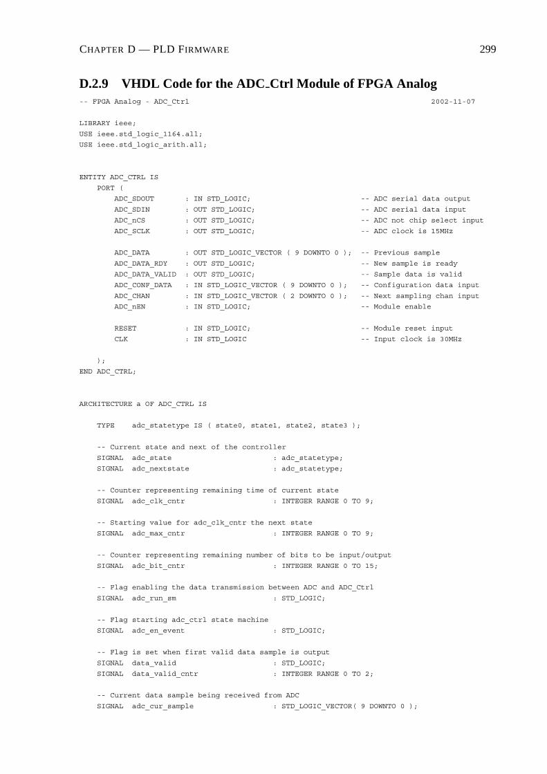
CHAPTER D — PLD FIRMWARE 299
D.2.9 VHDL Code for the ADC Ctrl Module of FPGA Analog-- FPGA Analog - ADC_Ctrl 2002-11-07
LIBRARY ieee;
USE ieee.std_logic_1164.all;
USE ieee.std_logic_arith.all;
ENTITY ADC_CTRL IS
PORT (
ADC_SDOUT : IN STD_LOGIC; -- ADC serial data output
ADC_SDIN : OUT STD_LOGIC; -- ADC serial data input
ADC_nCS : OUT STD_LOGIC; -- ADC not chip select input
ADC_SCLK : OUT STD_LOGIC; -- ADC clock is 15MHz
ADC_DATA : OUT STD_LOGIC_VECTOR ( 9 DOWNTO 0 ); -- Previous sample
ADC_DATA_RDY : OUT STD_LOGIC; -- New sample is ready
ADC_DATA_VALID : OUT STD_LOGIC; -- Sample data is valid
ADC_CONF_DATA : IN STD_LOGIC_VECTOR ( 9 DOWNTO 0 ); -- Configuration data input
ADC_CHAN : IN STD_LOGIC_VECTOR ( 2 DOWNTO 0 ); -- Next sampling chan input
ADC_nEN : IN STD_LOGIC; -- Module enable
RESET : IN STD_LOGIC; -- Module reset input
CLK : IN STD_LOGIC -- Input clock is 30MHz
);
END ADC_CTRL;
ARCHITECTURE a OF ADC_CTRL IS
TYPE adc_statetype IS ( state0, state1, state2, state3 );
-- Current state and next of the controller
SIGNAL adc_state : adc_statetype;
SIGNAL adc_nextstate : adc_statetype;
-- Counter representing remaining time of current state
SIGNAL adc_clk_cntr : INTEGER RANGE 0 TO 9;
-- Starting value for adc_clk_cntr the next state
SIGNAL adc_max_cntr : INTEGER RANGE 0 TO 9;
-- Counter representing remaining number of bits to be input/output
SIGNAL adc_bit_cntr : INTEGER RANGE 0 TO 15;
-- Flag enabling the data transmission between ADC and ADC_Ctrl
SIGNAL adc_run_sm : STD_LOGIC;
-- Flag starting adc_ctrl state machine
SIGNAL adc_en_event : STD_LOGIC;
-- Flag is set when first valid data sample is output
SIGNAL data_valid : STD_LOGIC;
SIGNAL data_valid_cntr : INTEGER RANGE 0 TO 2;
-- Current data sample being received from ADC
SIGNAL adc_cur_sample : STD_LOGIC_VECTOR( 9 DOWNTO 0 );

CHAPTER D — PLD FIRMWARE 300
-- Current configuration outout data
SIGNAL adc_conf_data_out : STD_LOGIC_VECTOR( 15 DOWNTO 0 );
SIGNAL signal_ADC_nCS : STD_LOGIC;
SIGNAL signal_ADC_SCLK : STD_LOGIC;
BEGIN
ADC_nCS <= signal_ADC_nCS;
ADC_SCLK <= signal_ADC_SCLK WHEN ( adc_nEN = ’0’ ) ELSE
’0’;
data_valid <= ’0’ WHEN ( RESET = ’1’ ) ELSE
’1’ WHEN ( data_valid_cntr = 0 ) ELSE
’0’;
adc_conf_data_out( 15 DOWNTO 10 ) <= ADC_CONF_DATA( 9 DOWNTO 4 );
adc_conf_data_out( 9 DOWNTO 7 ) <= ADC_CHAN;
adc_conf_data_out( 6 DOWNTO 3 ) <= ADC_CONF_DATA( 3 DOWNTO 0 );
adc_conf_data_out( 2 DOWNTO 0 ) <= "000";
ADC_DATA_VALID <= data_valid;
adc_run_sm <= ’0’ WHEN RESET = ’1’ ELSE
’0’ WHEN ( adc_state = state0 )and
( adc_nEN = ’1’ ) ELSE
’1’ WHEN ( adc_en_event = ’1’ ) ELSE
’1’ WHEN ( adc_state /= state0 ) ELSE
adc_run_sm;
------------------------------------------------------------------------------------------
-- Process for generating data ready signal (Taking into account sample validity)
valid_data_proc:
PROCESS ( signal_ADC_SCLK , RESET )
BEGIN
IF ( RESET = ’1’ )or( ADC_nEN = ’1’) THEN
data_valid_cntr <= 3;
ADC_DATA_RDY <= ’0’;
ELSIF ( signal_ADC_SCLK’event )and( signal_ADC_SCLK = ’1’ ) THEN
IF ( adc_state = state0 ) THEN
ADC_DATA_RDY <= ’0’;
ELSIF ( adc_state = state3 )and( adc_bit_cntr = 0 ) THEN
IF ( data_valid_cntr > 0 ) THEN
data_valid_cntr <= data_valid_cntr-1;
ADC_DATA_RDY <= ’1’;
ELSE
data_valid_cntr <= 0;
ADC_DATA_RDY <= ’1’; --data_valid;
END IF;
END IF;
END IF;

CHAPTER D — PLD FIRMWARE 301
END PROCESS valid_data_proc;
------------------------------------------------------------------------------------------
-- Process for dividing the input clk f=30MHz by two to generate the ADC input
-- clk f=15MHz
adc_clk_proc:
PROCESS ( RESET, CLK )
BEGIN
IF ( RESET = ’1’ ) THEN
signal_ADC_SCLK <= ’1’;
ELSIF ( CLK’event )and( CLK = ’0’ ) THEN
signal_ADC_SCLK <= not( signal_ADC_SCLK );
END IF;
END PROCESS adc_clk_proc;
------------------------------------------------------------------------------------------
-- Process for updating the new sample data vector (ADC_DATA)
adc_WR_proc:
PROCESS ( signal_ADC_SCLK, RESET )
BEGIN
IF ( RESET = ’1’ ) THEN
ADC_DATA <= "0000000000";
ELSIF ( signal_ADC_SCLK’event )and( signal_ADC_SCLK = ’0’) THEN
IF ( adc_state = state0 ) THEN
ADC_DATA <= adc_cur_sample;
END IF;
END IF;
END PROCESS adc_WR_proc;
------------------------------------------------------------------------------------------
-- Process sampling the serial input from the ADC containg the new sample data
adc_SDOUT_proc:
PROCESS ( signal_ADC_SCLK )
BEGIN
IF ( signal_ADC_SCLK’event )and( signal_ADC_SCLK = ’0’ ) THEN
IF ( adc_state = state3 ) THEN
adc_cur_sample(adc_clk_cntr) <= ADC_SDOUT;
END IF;
END IF;
END PROCESS adc_SDOUT_proc;
------------------------------------------------------------------------------------------
-- Process which outputs the configuration data for the next ADC conversion

CHAPTER D — PLD FIRMWARE 302
adc_SDIN_proc:
PROCESS ( CLK, RESET )
BEGIN
IF ( RESET = ’1’ ) THEN
ADC_SDIN <= ’0’;
ELSIF ( CLK’event )and( CLK = ’1’ ) THEN
IF ( adc_state = state2)or( adc_state = state3 ) THEN
ADC_SDIN <= adc_conf_data_out(adc_bit_cntr);
ELSE
ADC_SDIN <= ’0’;
END IF;
END IF;
END PROCESS adc_SDIN_proc;
------------------------------------------------------------------------------------------
-- Process that generates the event that starts the state machine
adc_start_sm:
PROCESS ( RESET, ADC_nEN, adc_state )
BEGIN
IF ( RESET = ’1’ )or(adc_state = state2) THEN
adc_en_event <= ’0’;
ELSIF ( ADC_nEN’event )and( ADC_nEN = ’0’) THEN
adc_en_event <= ’1’;
END IF;
END PROCESS adc_start_sm;
------------------------------------------------------------------------------------------
-- Process that determines the sequence of the state machine states and their
-- durations
adc_sm_proc:
PROCESS ( adc_state )
BEGIN
CASE adc_state IS
WHEN state0 =>
signal_ADC_nCS <= ’1’;
adc_max_cntr <= 1;
adc_nextstate <= state1;
WHEN state1 =>
signal_ADC_nCS <= ’1’;
adc_max_cntr <= 5;
adc_nextstate <= state2;
WHEN state2 =>
signal_ADC_nCS <= ’0’;
adc_max_cntr <= 9;
CHAPTER D — PLD FIRMWARE 303
adc_nextstate <= state3;
WHEN state3 =>
signal_ADC_nCS <= ’0’;
adc_max_cntr <= 1;
adc_nextstate <= state0;
END CASE;
END PROCESS adc_sm_proc;
------------------------------------------------------------------------------------------
-- Process controls the transitions of the state machine from one state to the next
adc_proc:
PROCESS ( signal_ADC_SCLK, RESET )
BEGIN
IF ( RESET = ’1’ ) THEN
adc_bit_cntr <= 15;
adc_clk_cntr <= 1;
adc_state <= adc_statetype’left;
ELSIF ( signal_ADC_SCLK’event )and( signal_ADC_SCLK = ’1’ ) THEN
IF ( adc_run_sm = ’1’ )and( adc_clk_cntr > 0 )and
( ( adc_state = state2 )or( adc_state = state3 ) ) THEN
adc_bit_cntr <= adc_bit_cntr-1;
adc_clk_cntr <= adc_clk_cntr-1;
adc_state <= adc_state;
ELSIF ( adc_run_sm = ’1’ )and( adc_bit_cntr > 0 )and
( ( adc_state = state2 )or( adc_state = state3 ) ) THEN
adc_bit_cntr <= adc_bit_cntr-1;
adc_clk_cntr <= adc_max_cntr;
adc_state <= adc_nextstate;
ELSIF ( adc_run_sm = ’1’ ) THEN
adc_bit_cntr <= 15;
adc_clk_cntr <= adc_max_cntr;
adc_state <= adc_nextstate;
END IF;
END IF;
END PROCESS adc_proc;
END a;
CHAPTER D — PLD FIRMWARE 304
D.2.10 VHDL Code for the ADC Chan Generator Module of FPGA
Analog-- FPGA Analog - ADC_CHAN_GENERATOR 2002-11-07
LIBRARY ieee;
USE ieee.std_logic_1164.all;
USE ieee.std_logic_arith.all;
ENTITY ADC_CHAN_GENERATOR IS
PORT (
CHAN_OUT : OUT STD_LOGIC_VECTOR ( 2 DOWNTO 0 );
DATA_RDY : IN STD_LOGIC;
SAMP_CHAN0 : IN STD_LOGIC_VECTOR ( 2 DOWNTO 0 );
SAMP_CHAN1 : IN STD_LOGIC_VECTOR ( 2 DOWNTO 0 );
SAMP_CHAN2 : IN STD_LOGIC_VECTOR ( 2 DOWNTO 0 );
SAMP_CHAN3 : IN STD_LOGIC_VECTOR ( 2 DOWNTO 0 );
SAMP_CHAN4 : IN STD_LOGIC_VECTOR ( 2 DOWNTO 0 );
SAMP_CHAN5 : IN STD_LOGIC_VECTOR ( 2 DOWNTO 0 );
SAMP_CHAN6 : IN STD_LOGIC_VECTOR ( 2 DOWNTO 0 );
SAMP_CHAN7 : IN STD_LOGIC_VECTOR ( 2 DOWNTO 0 );
RESET : IN STD_LOGIC
);
END ADC_CHAN_GENERATOR;
ARCHITECTURE a OF ADC_CHAN_GENERATOR IS
SIGNAL next_chan : INTEGER RANGE 0 TO 7;
BEGIN
CHAN_OUT <= SAMP_CHAN0 WHEN ( next_chan = 0 ) ELSE
SAMP_CHAN1 WHEN ( next_chan = 1 ) ELSE
SAMP_CHAN2 WHEN ( next_chan = 2 ) ELSE
SAMP_CHAN3 WHEN ( next_chan = 3 ) ELSE
SAMP_CHAN4 WHEN ( next_chan = 4 ) ELSE
SAMP_CHAN5 WHEN ( next_chan = 5 ) ELSE
SAMP_CHAN6 WHEN ( next_chan = 6 ) ELSE
SAMP_CHAN7 WHEN ( next_chan = 7 ) ELSE
"000";
adc_chan_proc:
PROCESS ( DATA_RDY, RESET )
BEGIN
IF ( RESET = ’1’ ) THEN
next_chan <= 0;
ELSIF ( DATA_RDY’event )and( DATA_RDY = ’0’ ) THEN
IF ( next_chan < 7 ) THEN
next_chan <= next_chan + 1;
ELSE

CHAPTER D — PLD FIRMWARE 305
next_chan <= 0;
END IF;
END IF;
END PROCESS;
END a;

CHAPTER D — PLD FIRMWARE 306
D.2.11 VHDL Code for the ADC Data Store Module of FPGA Analog-- FPGA Analog - ADC_DATA_STORE 2002-11-13
LIBRARY ieee;
USE ieee.std_logic_1164.all;
USE ieee.std_logic_arith.all;
ENTITY ADC_DATA_STORE IS
PORT (
DATA_IN : IN STD_LOGIC_VECTOR ( 9 DOWNTO 0 );
CHAN_IN : IN STD_LOGIC_VECTOR ( 2 DOWNTO 0 );
DATA_RDY : IN STD_LOGIC;
DATA_VALID : IN STD_LOGIC;
DATA_OUT : OUT STD_LOGIC_VECTOR ( 12 DOWNTO 0 );
RESET : IN STD_LOGIC
);
END ADC_DATA_STORE;
ARCHITECTURE a OF ADC_DATA_STORE IS
SIGNAL next_chan, cur_chan : STD_LOGIC_VECTOR( 2 DOWNTO 0 );
BEGIN
DATA_OUT( 9 DOWNTO 0 ) <= DATA_IN WHEN ( DATA_VALID = ’1’ );
adc_data_store_proc:
PROCESS ( DATA_RDY, RESET )
BEGIN
IF ( RESET = ’1’ ) THEN
cur_chan <= "000";
next_chan <= "000";
ELSIF ( DATA_RDY’event )and( DATA_RDY = ’1’ ) THEN
next_chan <= cur_chan;
cur_chan <= CHAN_IN;
DATA_OUT( 12 DOWNTO 10 ) <= cur_chan;
END IF;
END PROCESS;
END a;

CHAPTER D — PLD FIRMWARE 307
D.2.12 VHDL Code for the DAC Ctrl Module of FPGA Analog-- FPGA Analog - DAC_Ctrl 2002-11-13
LIBRARY ieee;
USE ieee.std_logic_1164.all;
USE ieee.std_logic_arith.all;
ENTITY DAC_CTRL IS
PORT (
DAC_SDIN : OUT STD_LOGIC;
DAC_nSYNC : OUT STD_LOGIC;
DAC_SCLK : OUT STD_LOGIC; -- DAC clock is 15MHz
DAC_nLDAC : OUT STD_LOGIC;
DAC_A_CONF_DATA : IN STD_LOGIC_VECTOR ( 14 DOWNTO 12 );
DAC_A_DATA : IN STD_LOGIC_VECTOR ( 11 DOWNTO 0 );
DAC_B_CONF_DATA : IN STD_LOGIC_VECTOR ( 14 DOWNTO 12 );
DAC_B_DATA : IN STD_LOGIC_VECTOR ( 11 DOWNTO 0 );
DAC_CTRL_DATA : IN STD_LOGIC_VECTOR ( 1 DOWNTO 0 );
DAC_nLOAD : IN STD_LOGIC;
RESET : IN STD_LOGIC;
CLK : IN STD_LOGIC -- Input clock is 30MHz
);
END DAC_CTRL;
ARCHITECTURE a OF DAC_CTRL IS
TYPE dac_statetype IS ( state0, state1, state2, state3, state4, state5 );
SIGNAL outputdata : STD_LOGIC_VECTOR ( 15 DOWNTO 0 );
SIGNAL dac_state : dac_statetype;
SIGNAL dac_nextstate : dac_statetype;
SIGNAL dac_max_cntr : INTEGER RANGE 0 TO 15;
SIGNAL dac_bit_cntr : INTEGER RANGE 0 TO 15;
SIGNAL dac_run_sm : STD_LOGIC;
SIGNAL dac_en_event : STD_LOGIC;
SIGNAL sclk_en : STD_LOGIC;
SIGNAL signal_sclk : STD_LOGIC;
SIGNAL signal_DAC_nSYNC : STD_LOGIC;
BEGIN
DAC_nLDAC <= ’0’ WHEN dac_state = state5 ELSE
’1’;
DAC_nSYNC <= signal_DAC_nSYNC;
DAC_SCLK <= signal_sclk WHEN ( sclk_en = ’1’ )and
( dac_run_sm = ’1’ )and
( DAC_CTRL_DATA /= "00" ) ELSE
’0’;
dac_run_sm <= ’0’ WHEN ( RESET = ’1’ ) ELSE
’1’ WHEN ( dac_en_event = ’0’ ) ELSE
CHAPTER D — PLD FIRMWARE 308
’1’ WHEN ( dac_state /= state0 ) ELSE
’0’;
outputdata( 11 DOWNTO 0 ) <= DAC_A_DATA WHEN ( dac_state = state2 ) ELSE
DAC_B_DATA WHEN ( dac_state = state4 ) ELSE
"000000000000";
outputdata( 14 DOWNTO 12 ) <= DAC_A_CONF_DATA WHEN ( dac_state = state2 ) ELSE
DAC_B_CONF_DATA WHEN ( dac_state = state4 ) ELSE
"000";
outputdata( 15 ) <= ’0’ WHEN ( DAC_CTRL_DATA = "01" ) ELSE
’1’ WHEN ( DAC_CTRL_DATA = "10" ) ELSE
’0’ WHEN ( DAC_CTRL_DATA = "11" )and
( dac_nextstate = state2 ) ELSE
’1’ WHEN ( DAC_CTRL_DATA = "11" )and
( dac_nextstate = state4 ) ELSE
’0’;
------------------------------------------------------------------------------------------
dac_sclk_en_proc:
PROCESS ( CLK, RESET )
BEGIN
IF ( RESET = ’1’ ) THEN
sclk_en <= ’0’;
ELSIF ( CLK’event )and( CLK = ’1’ ) THEN
IF ( dac_state = state2 )or( dac_state = state4 )or
( ( dac_state = state1 )and( dac_bit_cntr = 0) )or
( ( dac_state = state3 )and( dac_bit_cntr = 0) ) THEN
sclk_en <= ’1’;
ELSE
sclk_en <= ’0’;
END IF;
END IF;
END PROCESS dac_sclk_en_proc;
------------------------------------------------------------------------------------------
dac_sclk_proc:
PROCESS ( CLK, RESET )
BEGIN
IF ( RESET = ’1’ ) THEN
signal_sclk <= ’0’;
ELSIF ( CLK’event )and( CLK = ’1’ ) THEN
signal_sclk <= not ( signal_sclk );
END IF;
END PROCESS dac_sclk_proc;

CHAPTER D — PLD FIRMWARE 309
------------------------------------------------------------------------------------------
nsync_proc:
PROCESS ( CLK, RESET )
BEGIN
IF ( RESET = ’1’ ) THEN
signal_DAC_nSYNC <= ’1’;
ELSIF ( CLK’event )and( CLK = ’1’ ) THEN
IF ( dac_state = state2 )or( dac_state = state4)or
( ( dac_state = state1 )and( dac_bit_cntr = 0 ) )or
( ( dac_state = state3 )and( dac_bit_cntr = 0 ) ) THEN
signal_DAC_nSYNC <= ’0’;
ELSE
signal_DAC_nSYNC <= ’1’;
END IF;
END IF;
END PROCESS nsync_proc;
------------------------------------------------------------------------------------------
dac_start_sm:
PROCESS ( RESET, DAC_nLOAD, dac_state )
BEGIN
IF ( RESET = ’1’ )or(dac_state = state1) THEN
dac_en_event <= ’1’;
ELSIF ( DAC_nLOAD’event )and( DAC_nLOAD = ’0’) THEN
dac_en_event <= ’0’;
END IF;
END PROCESS dac_start_sm;
------------------------------------------------------------------------------------------
-- State machine process of DAC
dac_sm_proc:
PROCESS ( dac_state, DAC_CTRL_DATA )
BEGIN
CASE dac_state IS
WHEN state0 =>
dac_max_cntr <= 1;
dac_nextstate <= state1;
WHEN state1 =>
IF ( DAC_CTRL_DATA = "00" ) THEN
dac_nextstate <= state0;
dac_max_cntr <= 0;
ELSIF ( DAC_CTRL_DATA = "01" )or( DAC_CTRL_DATA = "11" ) THEN

CHAPTER D — PLD FIRMWARE 310
dac_nextstate <= state2;
dac_max_cntr <= 14;
ELSE
dac_nextstate <= state4;
dac_max_cntr <= 14;
END IF;
WHEN state2 =>
IF ( DAC_CTRL_DATA = "01" ) THEN
dac_nextstate <= state5;
dac_max_cntr <= 1;
ELSE
dac_nextstate <= state3;
dac_max_cntr <= 1;
END IF;
WHEN state3 =>
dac_max_cntr <= 14;
dac_nextstate <= state4;
WHEN state4 =>
dac_max_cntr <= 1;
dac_nextstate <= state5;
WHEN state5 =>
dac_max_cntr <= 0;
dac_nextstate <= state0;
END CASE;
END PROCESS dac_sm_proc;
------------------------------------------------------------------------------------------
dac_SDIN_proc:
PROCESS ( CLK, RESET )
BEGIN
IF ( RESET = ’1’ ) THEN
DAC_SDIN <= ’0’;
ELSIF ( CLK’event )and( CLK = ’1’ ) THEN
IF ( dac_state = state1 )or( dac_state = state3 ) THEN
DAC_SDIN <= outputdata( 15 );
ELSIF ( dac_state = state2 )or( dac_state = state4 ) THEN
DAC_SDIN <= outputdata( dac_bit_cntr );
ELSE
DAC_SDIN <= ’0’;
END IF;
END IF;
END PROCESS dac_SDIN_proc;

CHAPTER D — PLD FIRMWARE 311
------------------------------------------------------------------------------------------
dac_proc:
PROCESS ( signal_sclk, RESET )
BEGIN
IF ( RESET = ’1’ ) THEN
dac_state <= dac_statetype’left;
dac_bit_cntr <= 0;
ELSIF ( signal_sclk’event )and( signal_sclk = ’0’ ) THEN
IF ( dac_bit_cntr > 0 )and( dac_run_sm = ’1’ ) THEN
dac_bit_cntr <= dac_bit_cntr-1;
dac_state <= dac_state;
ELSIF ( dac_run_sm = ’1’ ) THEN
dac_bit_cntr <= dac_max_cntr;
dac_state <= dac_nextstate;
END IF;
END IF;
END PROCESS dac_proc;
END a;
CHAPTER D — PLD FIRMWARE 312
D.2.13 VHDL Code for the PWM Ctrl Module of FPGA Analog-- FPGA Analog - PWM Controller 2002-11-07
LIBRARY ieee;
USE ieee.std_logic_1164.all;
USE ieee.std_logic_arith.all;
ENTITY pwm_ctrl IS
PORT (
PWMA_TOP : OUT STD_LOGIC;
PWMA_BOT : OUT STD_LOGIC;
PWMB_TOP : OUT STD_LOGIC;
PWMB_BOT : OUT STD_LOGIC;
PWMC_TOP : OUT STD_LOGIC;
PWMC_BOT : OUT STD_LOGIC;
PWMN_TOP : OUT STD_LOGIC;
PWMN_BOT : OUT STD_LOGIC;
ERRA_TOP : IN STD_LOGIC;
ERRA_BOT : IN STD_LOGIC;
ERRB_TOP : IN STD_LOGIC;
ERRB_BOT : IN STD_LOGIC;
ERRC_TOP : IN STD_LOGIC;
ERRC_BOT : IN STD_LOGIC;
ERRN_TOP : IN STD_LOGIC;
ERRN_BOT : IN STD_LOGIC;
TriMax : IN STD_LOGIC_VECTOR ( 9 DOWNTO 0 );
TriFreqScale : IN STD_LOGIC_VECTOR ( 9 DOWNTO 0 );
DeadTime : IN STD_LOGIC_VECTOR ( 9 DOWNTO 0 );
RefA : IN STD_LOGIC_VECTOR ( 9 DOWNTO 0 );
RefB : IN STD_LOGIC_VECTOR ( 9 DOWNTO 0 );
RefC : IN STD_LOGIC_VECTOR ( 9 DOWNTO 0 );
RefN : IN STD_LOGIC_VECTOR ( 9 DOWNTO 0 );
CompUpVal : IN STD_LOGIC_VECTOR ( 9 DOWNTO 0 );
CompDownVal : IN STD_LOGIC_VECTOR ( 9 DOWNTO 0 );
CompUp : OUT STD_LOGIC;
CompDown : OUT STD_LOGIC;
RampDir : OUT STD_LOGIC;
CounterZero : OUT STD_LOGIC;
PWM_nEN : IN STD_LOGIC;
RESET : IN STD_LOGIC;
CLK : IN STD_LOGIC
);
END pwm_ctrl;
ARCHITECTURE a OF pwm_ctrl IS
TYPE gate_state_type IS ( topstate, deadstate, botstate );
SIGNAL slow_clk : STD_LOGIC;
SIGNAL clk_cntr : INTEGER RANGE 0 TO 1023;
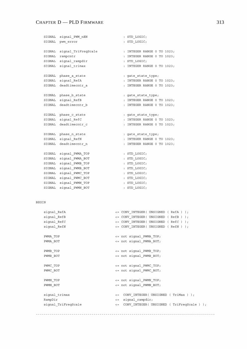
CHAPTER D — PLD FIRMWARE 313
SIGNAL signal_PWM_nEN : STD_LOGIC;
SIGNAL pwm_error : STD_LOGIC;
SIGNAL signal_TriFreqScale : INTEGER RANGE 0 TO 1023;
SIGNAL rampcntr : INTEGER RANGE 0 TO 1023;
SIGNAL signal_rampdir : STD_LOGIC;
SIGNAL signal_trimax : INTEGER RANGE 0 TO 1023;
SIGNAL phase_a_state : gate_state_type;
SIGNAL signal_RefA : INTEGER RANGE 0 TO 1023;
SIGNAL deadtimecntr_a : INTEGER RANGE 0 TO 1023;
SIGNAL phase_b_state : gate_state_type;
SIGNAL signal_RefB : INTEGER RANGE 0 TO 1023;
SIGNAL deadtimecntr_b : INTEGER RANGE 0 TO 1023;
SIGNAL phase_c_state : gate_state_type;
SIGNAL signal_RefC : INTEGER RANGE 0 TO 1023;
SIGNAL deadtimecntr_c : INTEGER RANGE 0 TO 1023;
SIGNAL phase_n_state : gate_state_type;
SIGNAL signal_RefN : INTEGER RANGE 0 TO 1023;
SIGNAL deadtimecntr_n : INTEGER RANGE 0 TO 1023;
SIGNAL signal_PWMA_TOP : STD_LOGIC;
SIGNAL signal_PWMA_BOT : STD_LOGIC;
SIGNAL signal_PWMB_TOP : STD_LOGIC;
SIGNAL signal_PWMB_BOT : STD_LOGIC;
SIGNAL signal_PWMC_TOP : STD_LOGIC;
SIGNAL signal_PWMC_BOT : STD_LOGIC;
SIGNAL signal_PWMN_TOP : STD_LOGIC;
SIGNAL signal_PWMN_BOT : STD_LOGIC;
BEGIN
signal_RefA <= CONV_INTEGER( UNSIGNED ( RefA ) );
signal_RefB <= CONV_INTEGER( UNSIGNED ( RefB ) );
signal_RefC <= CONV_INTEGER( UNSIGNED ( RefC ) );
signal_RefN <= CONV_INTEGER( UNSIGNED ( RefN ) );
PWMA_TOP <= not signal_PWMA_TOP;
PWMA_BOT <= not signal_PWMA_BOT;
PWMB_TOP <= not signal_PWMB_TOP;
PWMB_BOT <= not signal_PWMB_BOT;
PWMC_TOP <= not signal_PWMC_TOP;
PWMC_BOT <= not signal_PWMC_BOT;
PWMN_TOP <= not signal_PWMN_TOP;
PWMN_BOT <= not signal_PWMN_BOT;
signal_trimax <= CONV_INTEGER( UNSIGNED ( TriMax ) );
RampDir <= signal_rampdir;
signal_TriFreqScale <= CONV_INTEGER( UNSIGNED ( TriFreqScale ) );
------------------------------------------------------------------------------------------

CHAPTER D — PLD FIRMWARE 314
ref_proc:
PROCESS ( CLK, RESET )
BEGIN
IF ( RESET = ’1’ ) THEN
CounterZero <= ’1’;
ELSIF ( CLK’event )and( CLK = ’1’ ) THEN
IF ( rampcntr = 0 ) THEN
CounterZero <= ’1’;
ELSE
CounterZero <= ’0’;
END IF;
END IF;
END PROCESS ref_proc;
------------------------------------------------------------------------------------------
phase_a_sm_ctrl_proc:
PROCESS ( slow_clk, RESET )
BEGIN
IF ( RESET = ’1’ ) THEN
signal_PWMA_TOP <= ’0’;
signal_PWMA_BOT <= ’0’;
deadtimecntr_a <= 0;
phase_a_state <= topstate;
ELSIF ( slow_clk’event )and( slow_clk = ’1’ ) THEN
IF ( signal_PWM_nEN = ’1’ ) THEN
phase_a_state <= topstate;
signal_PWMA_TOP <= ’0’;
signal_PWMA_BOT <= ’0’;
deadtimecntr_a <= 0;
ELSIF ( phase_a_state = topstate )and( rampcntr < signal_RefA ) THEN
phase_a_state <= topstate;
signal_PWMA_TOP <= ’1’;
signal_PWMA_BOT <= ’0’;
deadtimecntr_a <= 0;
ELSIF ( phase_a_state = topstate ) THEN
phase_a_state <= deadstate;
signal_PWMA_TOP <= ’0’;
signal_PWMA_BOT <= ’0’;
deadtimecntr_a <= deadtimecntr_a + 1;
ELSIF ( phase_a_state = deadstate )and
( deadtimecntr_a < CONV_INTEGER( UNSIGNED ( DeadTime ) ) )and
( signal_rampdir = ’1’ ) THEN
phase_a_state <= deadstate;
signal_PWMA_TOP <= ’0’;
signal_PWMA_BOT <= ’0’;
deadtimecntr_a <= deadtimecntr_a + 1;
ELSIF ( phase_a_state = deadstate )and( signal_rampdir = ’1’ ) THEN

CHAPTER D — PLD FIRMWARE 315
phase_a_state <= botstate;
signal_PWMA_TOP <= ’0’;
signal_PWMA_BOT <= ’1’;
deadtimecntr_a <= 0;
ELSIF ( phase_a_state = botstate )and( rampcntr > signal_RefA ) THEN
phase_a_state <= botstate;
signal_PWMA_TOP <= ’0’;
signal_PWMA_BOT <= ’1’;
deadtimecntr_a <= 0;
ELSIF ( phase_a_state = botstate ) THEN
phase_a_state <= deadstate;
signal_PWMA_TOP <= ’0’;
signal_PWMA_BOT <= ’0’;
deadtimecntr_a <= 0;
ELSIF ( phase_a_state = deadstate )and
( deadtimecntr_a < CONV_INTEGER( UNSIGNED ( DeadTime ) ) )and
( signal_rampdir = ’0’ ) THEN
phase_a_state <= deadstate;
signal_PWMA_TOP <= ’0’;
signal_PWMA_BOT <= ’0’;
deadtimecntr_a <= deadtimecntr_a + 1;
ELSIF ( phase_a_state = deadstate )and( signal_rampdir = ’0’ ) THEN
phase_a_state <= topstate;
signal_PWMA_TOP <= ’1’;
signal_PWMA_BOT <= ’0’;
deadtimecntr_a <= 0;
END IF;
END IF;
END PROCESS phase_a_sm_ctrl_proc;
------------------------------------------------------------------------------------------
phase_b_sm_ctrl_proc:
PROCESS ( slow_clk, RESET )
BEGIN
IF ( RESET = ’1’ ) THEN
signal_PWMB_TOP <= ’0’;
signal_PWMB_BOT <= ’0’;
deadtimecntr_b <= 0;
phase_b_state <= topstate;
ELSIF ( slow_clk’event )and( slow_clk = ’1’ ) THEN
IF ( signal_PWM_nEN = ’1’ ) THEN
phase_b_state <= topstate;
signal_PWMB_TOP <= ’0’;
signal_PWMB_BOT <= ’0’;
deadtimecntr_b <= 0;
ELSIF ( phase_b_state = topstate )and( rampcntr < signal_RefB ) THEN
phase_b_state <= topstate;
signal_PWMB_TOP <= ’1’;
signal_PWMB_BOT <= ’0’;
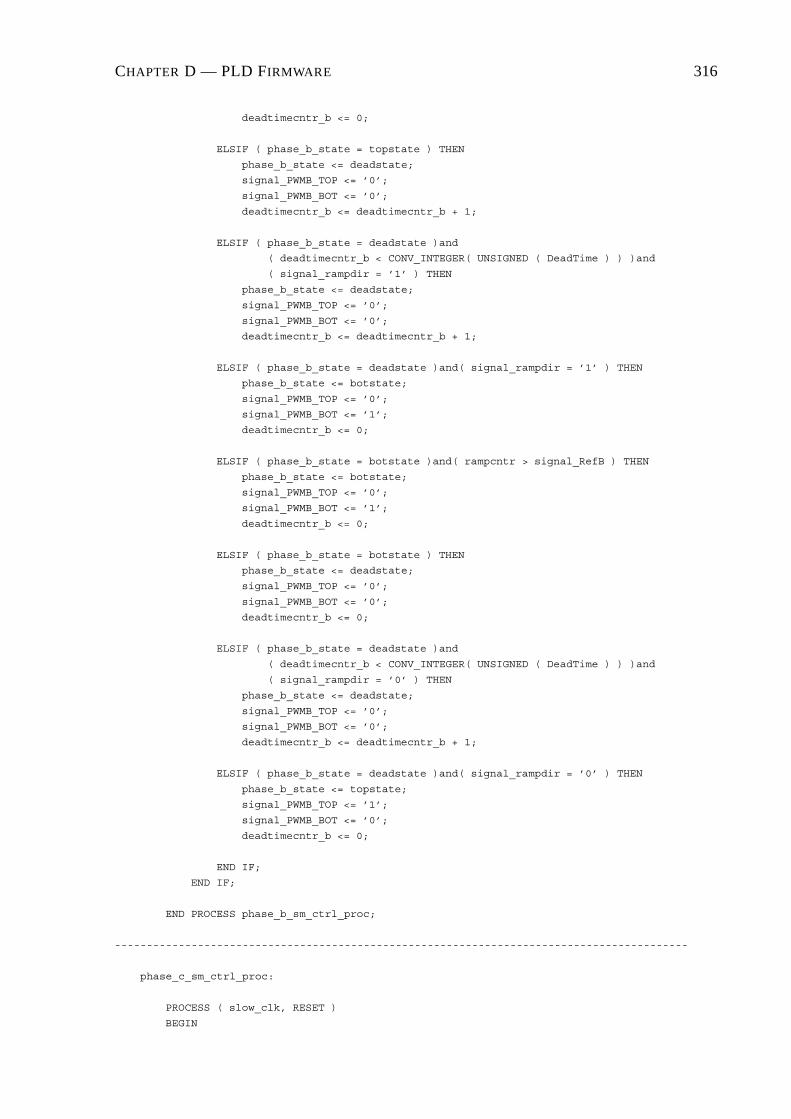
CHAPTER D — PLD FIRMWARE 316
deadtimecntr_b <= 0;
ELSIF ( phase_b_state = topstate ) THEN
phase_b_state <= deadstate;
signal_PWMB_TOP <= ’0’;
signal_PWMB_BOT <= ’0’;
deadtimecntr_b <= deadtimecntr_b + 1;
ELSIF ( phase_b_state = deadstate )and
( deadtimecntr_b < CONV_INTEGER( UNSIGNED ( DeadTime ) ) )and
( signal_rampdir = ’1’ ) THEN
phase_b_state <= deadstate;
signal_PWMB_TOP <= ’0’;
signal_PWMB_BOT <= ’0’;
deadtimecntr_b <= deadtimecntr_b + 1;
ELSIF ( phase_b_state = deadstate )and( signal_rampdir = ’1’ ) THEN
phase_b_state <= botstate;
signal_PWMB_TOP <= ’0’;
signal_PWMB_BOT <= ’1’;
deadtimecntr_b <= 0;
ELSIF ( phase_b_state = botstate )and( rampcntr > signal_RefB ) THEN
phase_b_state <= botstate;
signal_PWMB_TOP <= ’0’;
signal_PWMB_BOT <= ’1’;
deadtimecntr_b <= 0;
ELSIF ( phase_b_state = botstate ) THEN
phase_b_state <= deadstate;
signal_PWMB_TOP <= ’0’;
signal_PWMB_BOT <= ’0’;
deadtimecntr_b <= 0;
ELSIF ( phase_b_state = deadstate )and
( deadtimecntr_b < CONV_INTEGER( UNSIGNED ( DeadTime ) ) )and
( signal_rampdir = ’0’ ) THEN
phase_b_state <= deadstate;
signal_PWMB_TOP <= ’0’;
signal_PWMB_BOT <= ’0’;
deadtimecntr_b <= deadtimecntr_b + 1;
ELSIF ( phase_b_state = deadstate )and( signal_rampdir = ’0’ ) THEN
phase_b_state <= topstate;
signal_PWMB_TOP <= ’1’;
signal_PWMB_BOT <= ’0’;
deadtimecntr_b <= 0;
END IF;
END IF;
END PROCESS phase_b_sm_ctrl_proc;
------------------------------------------------------------------------------------------
phase_c_sm_ctrl_proc:
PROCESS ( slow_clk, RESET )
BEGIN

CHAPTER D — PLD FIRMWARE 317
IF ( RESET = ’1’ ) THEN
signal_PWMC_TOP <= ’0’;
signal_PWMC_BOT <= ’0’;
deadtimecntr_c <= 0;
phase_c_state <= topstate;
ELSIF ( slow_clk’event )and( slow_clk = ’1’ ) THEN
IF ( signal_PWM_nEN = ’1’ ) THEN
phase_c_state <= topstate;
signal_PWMC_TOP <= ’0’;
signal_PWMC_BOT <= ’0’;
deadtimecntr_c <= 0;
ELSIF ( phase_c_state = topstate )and( rampcntr < signal_RefC ) THEN
phase_c_state <= topstate;
signal_PWMC_TOP <= ’1’;
signal_PWMC_BOT <= ’0’;
deadtimecntr_c <= 0;
ELSIF ( phase_c_state = topstate ) THEN
phase_c_state <= deadstate;
signal_PWMC_TOP <= ’0’;
signal_PWMC_BOT <= ’0’;
deadtimecntr_c <= deadtimecntr_c + 1;
ELSIF ( phase_c_state = deadstate )and
( deadtimecntr_c < CONV_INTEGER( UNSIGNED ( DeadTime ) ) )and
( signal_rampdir = ’1’ ) THEN
phase_c_state <= deadstate;
signal_PWMC_TOP <= ’0’;
signal_PWMC_BOT <= ’0’;
deadtimecntr_c <= deadtimecntr_c + 1;
ELSIF ( phase_c_state = deadstate )and( signal_rampdir = ’1’ ) THEN
phase_c_state <= botstate;
signal_PWMC_TOP <= ’0’;
signal_PWMC_BOT <= ’1’;
deadtimecntr_c <= 0;
ELSIF ( phase_c_state = botstate )and( rampcntr > signal_RefC ) THEN
phase_c_state <= botstate;
signal_PWMC_TOP <= ’0’;
signal_PWMC_BOT <= ’1’;
deadtimecntr_c <= 0;
ELSIF ( phase_c_state = botstate ) THEN
phase_c_state <= deadstate;
signal_PWMC_TOP <= ’0’;
signal_PWMC_BOT <= ’0’;
deadtimecntr_c <= 0;
ELSIF ( phase_c_state = deadstate )and
( deadtimecntr_c < CONV_INTEGER( UNSIGNED ( DeadTime ) ) )and
( signal_rampdir = ’0’ ) THEN
phase_c_state <= deadstate;
signal_PWMC_TOP <= ’0’;
signal_PWMC_BOT <= ’0’;
deadtimecntr_c <= deadtimecntr_c + 1;

CHAPTER D — PLD FIRMWARE 318
ELSIF ( phase_c_state = deadstate )and( signal_rampdir = ’0’ ) THEN
phase_c_state <= topstate;
signal_PWMC_TOP <= ’1’;
signal_PWMC_BOT <= ’0’;
deadtimecntr_c <= 0;
END IF;
END IF;
END PROCESS phase_c_sm_ctrl_proc;
------------------------------------------------------------------------------------------
phase_n_sm_ctrl_proc:
PROCESS ( slow_clk, RESET )
BEGIN
IF ( RESET = ’1’ ) THEN
signal_PWMN_TOP <= ’0’;
signal_PWMN_BOT <= ’0’;
deadtimecntr_n <= 0;
phase_n_state <= topstate;
ELSIF ( slow_clk’event )and( slow_clk = ’1’ ) THEN
IF ( signal_PWM_nEN = ’1’ ) THEN
phase_n_state <= topstate;
signal_PWMN_TOP <= ’0’;
signal_PWMN_BOT <= ’0’;
deadtimecntr_n <= 0;
ELSIF ( phase_n_state = topstate )and( rampcntr < signal_RefN ) THEN
phase_n_state <= topstate;
signal_PWMN_TOP <= ’1’;
signal_PWMN_BOT <= ’0’;
deadtimecntr_n <= 0;
ELSIF ( phase_n_state = topstate ) THEN
phase_n_state <= deadstate;
signal_PWMN_TOP <= ’0’;
signal_PWMN_BOT <= ’0’;
deadtimecntr_n <= deadtimecntr_n + 1;
ELSIF ( phase_n_state = deadstate )and
( deadtimecntr_n < CONV_INTEGER( UNSIGNED ( DeadTime ) ) )and
( signal_rampdir = ’1’ ) THEN
phase_n_state <= deadstate;
signal_PWMN_TOP <= ’0’;
signal_PWMN_BOT <= ’0’;
deadtimecntr_n <= deadtimecntr_n + 1;
ELSIF ( phase_n_state = deadstate )and( signal_rampdir = ’1’ ) THEN
phase_n_state <= botstate;
signal_PWMN_TOP <= ’0’;
signal_PWMN_BOT <= ’1’;
deadtimecntr_n <= 0;
ELSIF ( phase_n_state = botstate )and( rampcntr > signal_RefN ) THEN

CHAPTER D — PLD FIRMWARE 319
phase_n_state <= botstate;
signal_PWMN_TOP <= ’0’;
signal_PWMN_BOT <= ’1’;
deadtimecntr_n <= 0;
ELSIF ( phase_n_state = botstate ) THEN
phase_n_state <= deadstate;
signal_PWMN_TOP <= ’0’;
signal_PWMN_BOT <= ’0’;
deadtimecntr_n <= 0;
ELSIF ( phase_n_state = deadstate )and
( deadtimecntr_n < CONV_INTEGER( UNSIGNED ( DeadTime ) ) )and
( signal_rampdir = ’0’ ) THEN
phase_n_state <= deadstate;
signal_PWMN_TOP <= ’0’;
signal_PWMN_BOT <= ’0’;
deadtimecntr_n <= deadtimecntr_n + 1;
ELSIF ( phase_n_state = deadstate )and( signal_rampdir = ’0’ ) THEN
phase_n_state <= topstate;
signal_PWMN_TOP <= ’1’;
signal_PWMN_BOT <= ’0’;
deadtimecntr_n <= 0;
END IF;
END IF;
END PROCESS phase_n_sm_ctrl_proc;
------------------------------------------------------------------------------------------
compup_proc:
PROCESS ( CLK, RESET )
BEGIN
IF ( RESET = ’1’ ) THEN
CompUp <= ’0’;
ELSIF ( CLK’event )and( CLK = ’1’ ) THEN
IF ( signal_PWM_nEN = ’1’ ) THEN
CompUp <= ’0’;
ELSIF ( signal_rampdir = ’1’ )and
( rampcntr < CONV_INTEGER( UNSIGNED ( CompUpVal ) ) ) THEN
CompUp <= ’0’;
ELSIF ( rampcntr >= CONV_INTEGER( UNSIGNED ( CompUpVal ) ) ) THEN
CompUp <= ’1’;
END IF;
END IF;
END PROCESS compup_proc;
------------------------------------------------------------------------------------------
compdown_proc:

CHAPTER D — PLD FIRMWARE 320
PROCESS ( CLK, RESET )
BEGIN
IF ( RESET = ’1’ ) THEN
CompDown <= ’0’;
ELSIF ( CLK’event )and( CLK = ’1’ ) THEN
IF ( signal_PWM_nEN = ’1’ ) THEN
CompDown <= ’0’;
ELSIF ( signal_rampdir = ’1’ ) THEN
CompDown <= ’0’;
ELSIF ( signal_rampdir = ’0’ )and
( rampcntr <= CONV_INTEGER( UNSIGNED ( CompDownVal ) ) ) THEN
CompDown <= ’1’;
ELSIF ( rampcntr >= CONV_INTEGER( UNSIGNED ( CompDownVal ) ) ) THEN
CompDown <= ’0’;
END IF;
END IF;
END PROCESS compdown_proc;
------------------------------------------------------------------------------------------
pwm_error_proc:
PROCESS ( CLK, RESET )
BEGIN
IF ( RESET = ’1’ ) THEN
pwm_error <= ’0’;
ELSIF ( CLK’event )and( CLK = ’1’ ) THEN
IF ( ( signal_PWMA_TOP = ’1’ )and( signal_PWMA_BOT = ’1’ ) )or
( ( signal_PWMB_TOP = ’1’ )and( signal_PWMB_BOT = ’1’ ) )or
( ( signal_PWMC_TOP = ’1’ )and( signal_PWMC_BOT = ’1’ ) )or
( ( signal_PWMN_TOP = ’1’ )and( signal_PWMN_BOT = ’1’ ) ) THEN
pwm_error <= ’1’;
END IF;
END IF;
END PROCESS pwm_error_proc;
------------------------------------------------------------------------------------------
pwm_nen_proc:
PROCESS ( CLK, RESET, PWM_nEN )
BEGIN
IF ( RESET = ’1’ ) THEN
signal_PWM_nEN <= PWM_nEN;
ELSIF ( CLK’event )and( CLK = ’1’ ) THEN
IF ( pwm_error = ’1’ ) THEN
signal_PWM_nEN <= ’1’;
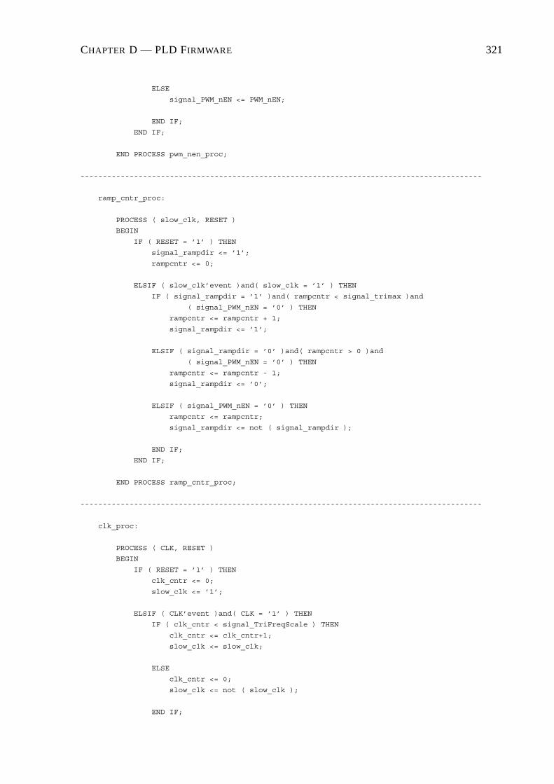
CHAPTER D — PLD FIRMWARE 321
ELSE
signal_PWM_nEN <= PWM_nEN;
END IF;
END IF;
END PROCESS pwm_nen_proc;
------------------------------------------------------------------------------------------
ramp_cntr_proc:
PROCESS ( slow_clk, RESET )
BEGIN
IF ( RESET = ’1’ ) THEN
signal_rampdir <= ’1’;
rampcntr <= 0;
ELSIF ( slow_clk’event )and( slow_clk = ’1’ ) THEN
IF ( signal_rampdir = ’1’ )and( rampcntr < signal_trimax )and
( signal_PWM_nEN = ’0’ ) THEN
rampcntr <= rampcntr + 1;
signal_rampdir <= ’1’;
ELSIF ( signal_rampdir = ’0’ )and( rampcntr > 0 )and
( signal_PWM_nEN = ’0’ ) THEN
rampcntr <= rampcntr - 1;
signal_rampdir <= ’0’;
ELSIF ( signal_PWM_nEN = ’0’ ) THEN
rampcntr <= rampcntr;
signal_rampdir <= not ( signal_rampdir );
END IF;
END IF;
END PROCESS ramp_cntr_proc;
------------------------------------------------------------------------------------------
clk_proc:
PROCESS ( CLK, RESET )
BEGIN
IF ( RESET = ’1’ ) THEN
clk_cntr <= 0;
slow_clk <= ’1’;
ELSIF ( CLK’event )and( CLK = ’1’ ) THEN
IF ( clk_cntr < signal_TriFreqScale ) THEN
clk_cntr <= clk_cntr+1;
slow_clk <= slow_clk;
ELSE
clk_cntr <= 0;
slow_clk <= not ( slow_clk );
END IF;

CHAPTER D — PLD FIRMWARE 322
END IF;
END PROCESS clk_proc;
END a;
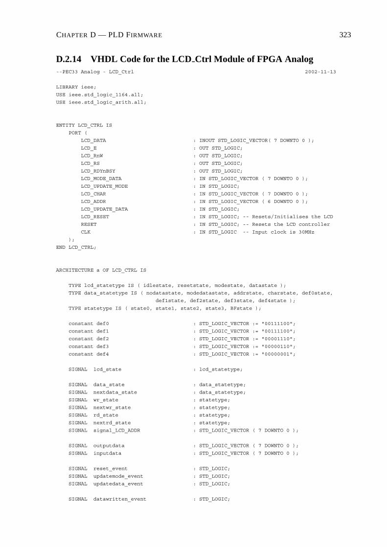
CHAPTER D — PLD FIRMWARE 323
D.2.14 VHDL Code for the LCD Ctrl Module of FPGA Analog--PEC33 Analog - LCD_Ctrl 2002-11-13
LIBRARY ieee;
USE ieee.std_logic_1164.all;
USE ieee.std_logic_arith.all;
ENTITY LCD_CTRL IS
PORT (
LCD_DATA : INOUT STD_LOGIC_VECTOR( 7 DOWNTO 0 );
LCD_E : OUT STD_LOGIC;
LCD_RnW : OUT STD_LOGIC;
LCD_RS : OUT STD_LOGIC;
LCD_RDYnBSY : OUT STD_LOGIC;
LCD_MODE_DATA : IN STD_LOGIC_VECTOR ( 7 DOWNTO 0 );
LCD_UPDATE_MODE : IN STD_LOGIC;
LCD_CHAR : IN STD_LOGIC_VECTOR ( 7 DOWNTO 0 );
LCD_ADDR : IN STD_LOGIC_VECTOR ( 6 DOWNTO 0 );
LCD_UPDATE_DATA : IN STD_LOGIC;
LCD_RESET : IN STD_LOGIC; -- Resets/Initialises the LCD
RESET : IN STD_LOGIC; -- Resets the LCD controller
CLK : IN STD_LOGIC -- Input clock is 30MHz
);
END LCD_CTRL;
ARCHITECTURE a OF LCD_CTRL IS
TYPE lcd_statetype IS ( idlestate, resetstate, modestate, datastate );
TYPE data_statetype IS ( nodatastate, modedatastate, addrstate, charstate, def0state,
def1state, def2state, def3state, def4state );
TYPE statetype IS ( state0, state1, state2, state3, BFstate );
constant def0 : STD_LOGIC_VECTOR := "00111100";
constant def1 : STD_LOGIC_VECTOR := "00111100";
constant def2 : STD_LOGIC_VECTOR := "00001110";
constant def3 : STD_LOGIC_VECTOR := "00000110";
constant def4 : STD_LOGIC_VECTOR := "00000001";
SIGNAL lcd_state : lcd_statetype;
SIGNAL data_state : data_statetype;
SIGNAL nextdata_state : data_statetype;
SIGNAL wr_state : statetype;
SIGNAL nextwr_state : statetype;
SIGNAL rd_state : statetype;
SIGNAL nextrd_state : statetype;
SIGNAL signal_LCD_ADDR : STD_LOGIC_VECTOR ( 7 DOWNTO 0 );
SIGNAL outputdata : STD_LOGIC_VECTOR ( 7 DOWNTO 0 );
SIGNAL inputdata : STD_LOGIC_VECTOR ( 7 DOWNTO 0 );
SIGNAL reset_event : STD_LOGIC;
SIGNAL updatemode_event : STD_LOGIC;
SIGNAL updatedata_event : STD_LOGIC;
SIGNAL datawritten_event : STD_LOGIC;
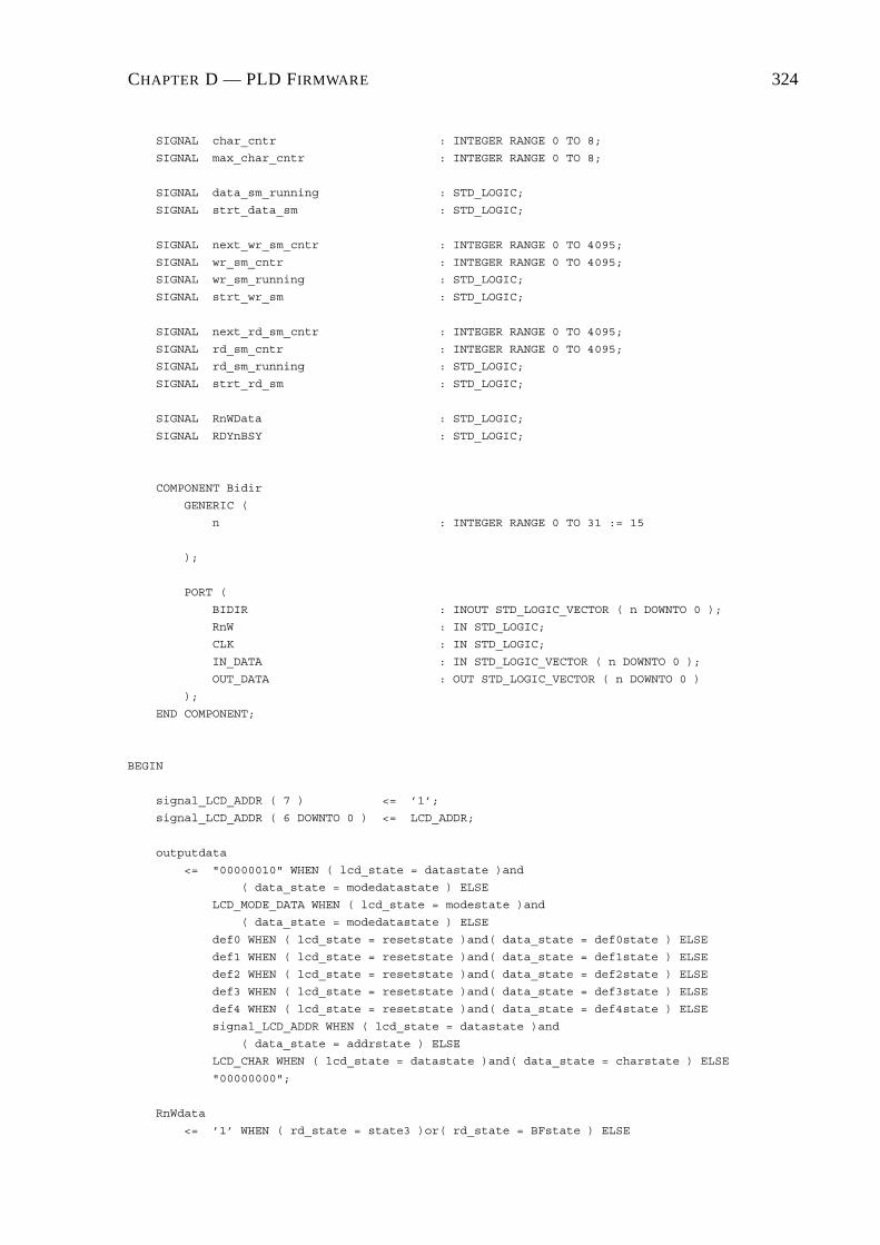
CHAPTER D — PLD FIRMWARE 324
SIGNAL char_cntr : INTEGER RANGE 0 TO 8;
SIGNAL max_char_cntr : INTEGER RANGE 0 TO 8;
SIGNAL data_sm_running : STD_LOGIC;
SIGNAL strt_data_sm : STD_LOGIC;
SIGNAL next_wr_sm_cntr : INTEGER RANGE 0 TO 4095;
SIGNAL wr_sm_cntr : INTEGER RANGE 0 TO 4095;
SIGNAL wr_sm_running : STD_LOGIC;
SIGNAL strt_wr_sm : STD_LOGIC;
SIGNAL next_rd_sm_cntr : INTEGER RANGE 0 TO 4095;
SIGNAL rd_sm_cntr : INTEGER RANGE 0 TO 4095;
SIGNAL rd_sm_running : STD_LOGIC;
SIGNAL strt_rd_sm : STD_LOGIC;
SIGNAL RnWData : STD_LOGIC;
SIGNAL RDYnBSY : STD_LOGIC;
COMPONENT Bidir
GENERIC (
n : INTEGER RANGE 0 TO 31 := 15
);
PORT (
BIDIR : INOUT STD_LOGIC_VECTOR ( n DOWNTO 0 );
RnW : IN STD_LOGIC;
CLK : IN STD_LOGIC;
IN_DATA : IN STD_LOGIC_VECTOR ( n DOWNTO 0 );
OUT_DATA : OUT STD_LOGIC_VECTOR ( n DOWNTO 0 )
);
END COMPONENT;
BEGIN
signal_LCD_ADDR ( 7 ) <= ’1’;
signal_LCD_ADDR ( 6 DOWNTO 0 ) <= LCD_ADDR;
outputdata
<= "00000010" WHEN ( lcd_state = datastate )and
( data_state = modedatastate ) ELSE
LCD_MODE_DATA WHEN ( lcd_state = modestate )and
( data_state = modedatastate ) ELSE
def0 WHEN ( lcd_state = resetstate )and( data_state = def0state ) ELSE
def1 WHEN ( lcd_state = resetstate )and( data_state = def1state ) ELSE
def2 WHEN ( lcd_state = resetstate )and( data_state = def2state ) ELSE
def3 WHEN ( lcd_state = resetstate )and( data_state = def3state ) ELSE
def4 WHEN ( lcd_state = resetstate )and( data_state = def4state ) ELSE
signal_LCD_ADDR WHEN ( lcd_state = datastate )and
( data_state = addrstate ) ELSE
LCD_CHAR WHEN ( lcd_state = datastate )and( data_state = charstate ) ELSE
"00000000";
RnWdata
<= ’1’ WHEN ( rd_state = state3 )or( rd_state = BFstate ) ELSE
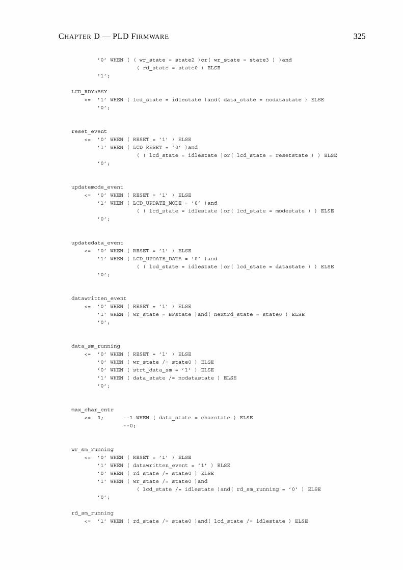
CHAPTER D — PLD FIRMWARE 325
’0’ WHEN ( ( wr_state = state2 )or( wr_state = state3 ) )and
( rd_state = state0 ) ELSE
’1’;
LCD_RDYnBSY
<= ’1’ WHEN ( lcd_state = idlestate )and( data_state = nodatastate ) ELSE
’0’;
reset_event
<= ’0’ WHEN ( RESET = ’1’ ) ELSE
’1’ WHEN ( LCD_RESET = ’0’ )and
( ( lcd_state = idlestate )or( lcd_state = resetstate ) ) ELSE
’0’;
updatemode_event
<= ’0’ WHEN ( RESET = ’1’ ) ELSE
’1’ WHEN ( LCD_UPDATE_MODE = ’0’ )and
( ( lcd_state = idlestate )or( lcd_state = modestate ) ) ELSE
’0’;
updatedata_event
<= ’0’ WHEN ( RESET = ’1’ ) ELSE
’1’ WHEN ( LCD_UPDATE_DATA = ’0’ )and
( ( lcd_state = idlestate )or( lcd_state = datastate ) ) ELSE
’0’;
datawritten_event
<= ’0’ WHEN ( RESET = ’1’ ) ELSE
’1’ WHEN ( wr_state = BFstate )and( nextrd_state = state0 ) ELSE
’0’;
data_sm_running
<= ’0’ WHEN ( RESET = ’1’ ) ELSE
’0’ WHEN ( wr_state /= state0 ) ELSE
’0’ WHEN ( strt_data_sm = ’1’ ) ELSE
’1’ WHEN ( data_state /= nodatastate ) ELSE
’0’;
max_char_cntr
<= 0; --1 WHEN ( data_state = charstate ) ELSE
--0;
wr_sm_running
<= ’0’ WHEN ( RESET = ’1’ ) ELSE
’1’ WHEN ( datawritten_event = ’1’ ) ELSE
’0’ WHEN ( rd_state /= state0 ) ELSE
’1’ WHEN ( wr_state /= state0 )and
( lcd_state /= idlestate )and( rd_sm_running = ’0’ ) ELSE
’0’;
rd_sm_running
<= ’1’ WHEN ( rd_state /= state0 )and( lcd_state /= idlestate ) ELSE

CHAPTER D — PLD FIRMWARE 326
’0’;
RDYnBSY
<= not ( inputdata(7) );
------------------------------------------------------------------------------------------
bidir_bus_map:
bidir GENERIC MAP ( n => 7 )
PORT MAP ( BIDIR => LCD_DATA, RnW => RnWdata, CLK => CLK,
IN_DATA => outputdata, OUT_DATA => inputdata );
------------------------------------------------------------------------------------------
lcd_rs_proc:
PROCESS ( CLK, RESET )
BEGIN
IF ( RESET = ’1’ ) THEN
LCD_RS <= ’0’;
ELSIF ( CLK’event )and( CLK = ’1’ ) THEN
IF ( data_state = charstate ) THEN
LCD_RS <= ’1’;
ELSE
LCD_RS <= ’0’;
END IF;
END IF;
END PROCESS lcd_rs_proc;
------------------------------------------------------------------------------------------
lcd_e_proc:
PROCESS ( CLK, RESET )
BEGIN
IF ( RESET = ’1’ ) THEN
LCD_E <= ’0’;
ELSIF ( CLK’event )and( CLK = ’1’ ) THEN
IF ( rd_state = state2 )or( wr_state = state2 ) THEN
LCD_E <= ’1’;
ELSE
LCD_E <= ’0’;
END IF;
END IF;
END PROCESS lcd_e_proc;
------------------------------------------------------------------------------------------
lcd_rnw_proc:
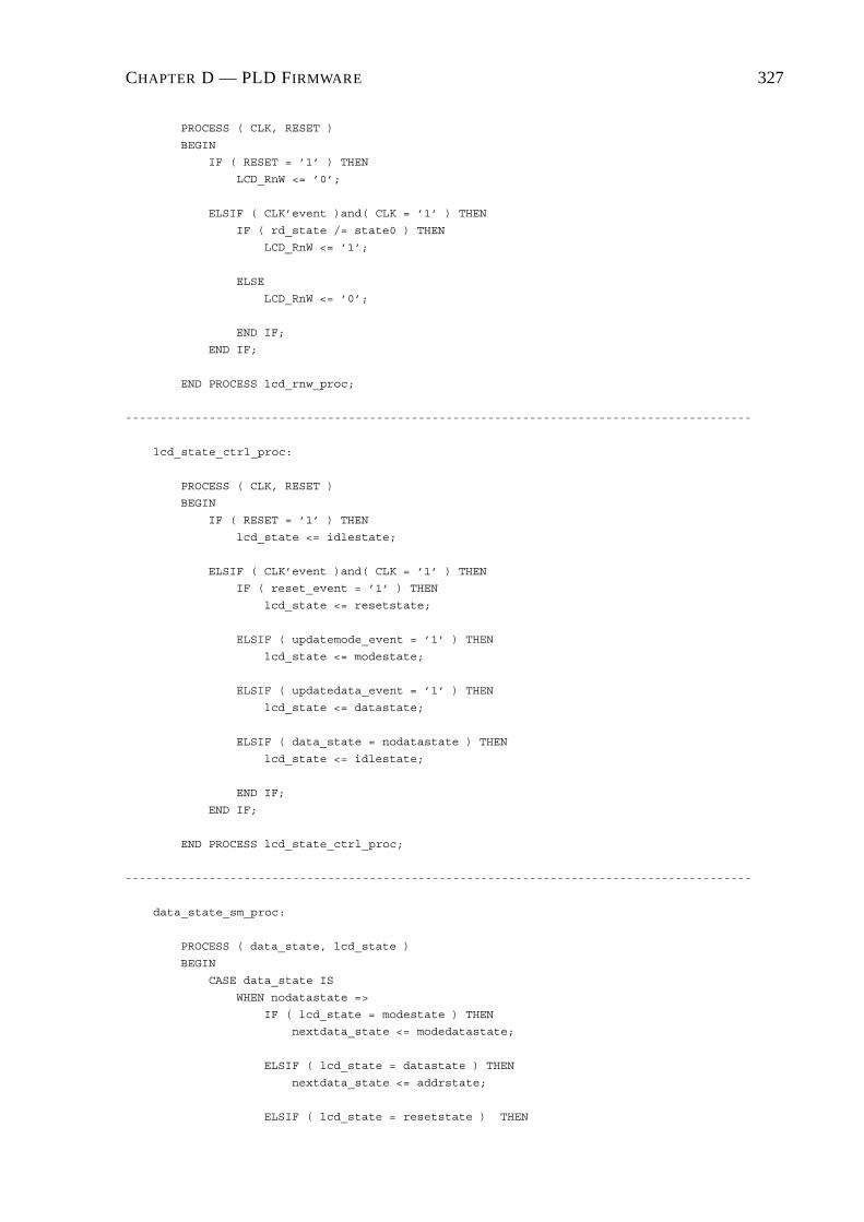
CHAPTER D — PLD FIRMWARE 327
PROCESS ( CLK, RESET )
BEGIN
IF ( RESET = ’1’ ) THEN
LCD_RnW <= ’0’;
ELSIF ( CLK’event )and( CLK = ’1’ ) THEN
IF ( rd_state /= state0 ) THEN
LCD_RnW <= ’1’;
ELSE
LCD_RnW <= ’0’;
END IF;
END IF;
END PROCESS lcd_rnw_proc;
------------------------------------------------------------------------------------------
lcd_state_ctrl_proc:
PROCESS ( CLK, RESET )
BEGIN
IF ( RESET = ’1’ ) THEN
lcd_state <= idlestate;
ELSIF ( CLK’event )and( CLK = ’1’ ) THEN
IF ( reset_event = ’1’ ) THEN
lcd_state <= resetstate;
ELSIF ( updatemode_event = ’1’ ) THEN
lcd_state <= modestate;
ELSIF ( updatedata_event = ’1’ ) THEN
lcd_state <= datastate;
ELSIF ( data_state = nodatastate ) THEN
lcd_state <= idlestate;
END IF;
END IF;
END PROCESS lcd_state_ctrl_proc;
------------------------------------------------------------------------------------------
data_state_sm_proc:
PROCESS ( data_state, lcd_state )
BEGIN
CASE data_state IS
WHEN nodatastate =>
IF ( lcd_state = modestate ) THEN
nextdata_state <= modedatastate;
ELSIF ( lcd_state = datastate ) THEN
nextdata_state <= addrstate;
ELSIF ( lcd_state = resetstate ) THEN

CHAPTER D — PLD FIRMWARE 328
nextdata_state <= def0state;
ELSE
nextdata_state <= nodatastate;
END IF;
WHEN modedatastate =>
nextdata_state <= nodatastate;
WHEN addrstate =>
nextdata_state <= charstate;
WHEN charstate =>
nextdata_state <= nodatastate;
WHEN def0state =>
nextdata_state <= def1state;
WHEN def1state =>
nextdata_state <= def2state;
WHEN def2state =>
nextdata_state <= def3state;
WHEN def3state =>
nextdata_state <= def4state;
WHEN def4state =>
nextdata_state <= nodatastate;
END CASE;
END PROCESS data_state_sm_proc;
------------------------------------------------------------------------------------------
data_sm_strt_proc:
PROCESS ( CLK, lcd_state, data_state, wr_state, reset_event, updatedata_event,
updatemode_event )
BEGIN
IF ( lcd_state /= idlestate )and( data_state = nodatastate )and
( wr_state = state0 )and( ( reset_event = ’1’ )or
( updatemode_event = ’1’ )or( updatedata_event = ’1’ ) ) THEN
strt_data_sm <= ’1’;
ELSIF ( CLK’event )and( CLK = ’1’ ) THEN
strt_data_sm <= ’0’;
END IF;
END PROCESS data_sm_strt_proc;
------------------------------------------------------------------------------------------
data_state_sm_ctrl:
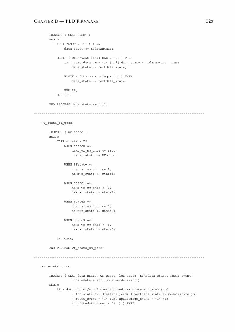
CHAPTER D — PLD FIRMWARE 329
PROCESS ( CLK, RESET )
BEGIN
IF ( RESET = ’1’ ) THEN
data_state <= nodatastate;
ELSIF ( CLK’event )and( CLK = ’1’ ) THEN
IF ( strt_data_sm = ’1’ )and( data_state = nodatastate ) THEN
data_state <= nextdata_state;
ELSIF ( data_sm_running = ’1’ ) THEN
data_state <= nextdata_state;
END IF;
END IF;
END PROCESS data_state_sm_ctrl;
------------------------------------------------------------------------------------------
wr_state_sm_proc:
PROCESS ( wr_state )
BEGIN
CASE wr_state IS
WHEN state0 =>
next_wr_sm_cntr <= 1500;
nextwr_state <= BFstate;
WHEN BFstate =>
next_wr_sm_cntr <= 1;
nextwr_state <= state1;
WHEN state1 =>
next_wr_sm_cntr <= 6;
nextwr_state <= state2;
WHEN state2 =>
next_wr_sm_cntr <= 8;
nextwr_state <= state3;
WHEN state3 =>
next_wr_sm_cntr <= 5;
nextwr_state <= state0;
END CASE;
END PROCESS wr_state_sm_proc;
------------------------------------------------------------------------------------------
wr_sm_strt_proc:
PROCESS ( CLK, data_state, wr_state, lcd_state, nextdata_state, reset_event,
updatedata_event, updatemode_event )
BEGIN
IF ( data_state /= nodatastate )and( wr_state = state0 )and
( lcd_state /= idlestate )and( ( nextdata_state /= nodatastate )or
( reset_event = ’1’ )or( updatemode_event = ’1’ )or
( updatedata_event = ’1’ ) ) THEN

CHAPTER D — PLD FIRMWARE 330
strt_wr_sm <= ’1’;
ELSIF ( CLK’event )and( CLK = ’0’ ) THEN
strt_wr_sm <= ’0’;
END IF;
END PROCESS wr_sm_strt_proc;
------------------------------------------------------------------------------------------
wr_state_sm_ctrl:
PROCESS ( CLK, RESET )
BEGIN
IF ( RESET = ’1’ ) THEN
wr_state <= state0;
wr_sm_cntr <= 1;
char_cntr <= 0;
ELSIF ( CLK’event )and( CLK = ’1’ ) THEN
IF ( strt_wr_sm = ’1’ ) THEN
wr_sm_cntr <= next_wr_sm_cntr;
wr_state <= nextwr_state;
ELSIF ( wr_sm_running = ’1’)and( wr_sm_cntr > 0 ) THEN
wr_sm_cntr <= wr_sm_cntr-1;
wr_state <= wr_state;
ELSIF ( wr_sm_running = ’1’) THEN
wr_sm_cntr <= next_wr_sm_cntr;
wr_state <= nextwr_state;
END IF;
END IF;
END PROCESS wr_state_sm_ctrl;
------------------------------------------------------------------------------------------
rd_state_sm_proc:
PROCESS ( rd_state, RDYnBSY )
BEGIN
CASE rd_state IS
WHEN state0 =>
next_rd_sm_cntr <= 1;
nextrd_state <= state1;
WHEN state1 =>
next_rd_sm_cntr <= 6;
nextrd_state <= state2;
WHEN state2 =>
next_rd_sm_cntr <= 8;
nextrd_state <= state3;
WHEN state3 =>
next_rd_sm_cntr <= 1500;

CHAPTER D — PLD FIRMWARE 331
nextrd_state <= BFstate;
WHEN BFstate =>
next_rd_sm_cntr <= 5;
nextrd_state <= state0;
END CASE;
END PROCESS rd_state_sm_proc;
------------------------------------------------------------------------------------------
rd_sm_strt_proc:
PROCESS ( CLK, rd_state, wr_state, lcd_state )
BEGIN
IF ( rd_state = state0 )and( wr_state = BFstate )and
( lcd_state /= idlestate ) THEN
strt_rd_sm <= ’1’;
ELSIF ( CLK’event )and( CLK = ’0’ ) THEN
strt_rd_sm <= ’0’;
END IF;
END PROCESS rd_sm_strt_proc;
------------------------------------------------------------------------------------------
rd_state_sm_ctrl:
PROCESS ( CLK, RESET )
BEGIN
IF ( RESET = ’1’ ) THEN
rd_state <= state0;
rd_sm_cntr <= 1;
ELSIF ( CLK’event )and( CLK = ’1’ ) THEN
IF ( strt_rd_sm = ’1’ ) THEN
rd_sm_cntr <= next_rd_sm_cntr;
rd_state <= nextrd_state;
ELSIF ( rd_sm_running = ’1’)and( rd_sm_cntr = 0 ) THEN
rd_sm_cntr <= next_rd_sm_cntr;
rd_state <= nextrd_state;
ELSIF ( rd_sm_running = ’1’) THEN
rd_sm_cntr <= rd_sm_cntr-1;
rd_state <= rd_state;
END IF;
END IF;
END PROCESS rd_state_sm_ctrl;
END a;

CHAPTER D — PLD FIRMWARE 332
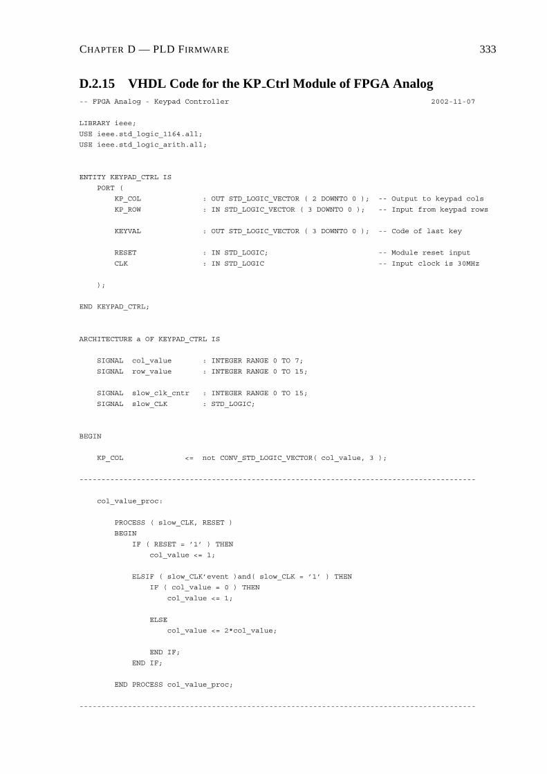
CHAPTER D — PLD FIRMWARE 333
D.2.15 VHDL Code for the KP Ctrl Module of FPGA Analog-- FPGA Analog - Keypad Controller 2002-11-07
LIBRARY ieee;
USE ieee.std_logic_1164.all;
USE ieee.std_logic_arith.all;
ENTITY KEYPAD_CTRL IS
PORT (
KP_COL : OUT STD_LOGIC_VECTOR ( 2 DOWNTO 0 ); -- Output to keypad cols
KP_ROW : IN STD_LOGIC_VECTOR ( 3 DOWNTO 0 ); -- Input from keypad rows
KEYVAL : OUT STD_LOGIC_VECTOR ( 3 DOWNTO 0 ); -- Code of last key
RESET : IN STD_LOGIC; -- Module reset input
CLK : IN STD_LOGIC -- Input clock is 30MHz
);
END KEYPAD_CTRL;
ARCHITECTURE a OF KEYPAD_CTRL IS
SIGNAL col_value : INTEGER RANGE 0 TO 7;
SIGNAL row_value : INTEGER RANGE 0 TO 15;
SIGNAL slow_clk_cntr : INTEGER RANGE 0 TO 15;
SIGNAL slow_CLK : STD_LOGIC;
BEGIN
KP_COL <= not CONV_STD_LOGIC_VECTOR( col_value, 3 );
------------------------------------------------------------------------------------------
col_value_proc:
PROCESS ( slow_CLK, RESET )
BEGIN
IF ( RESET = ’1’ ) THEN
col_value <= 1;
ELSIF ( slow_CLK’event )and( slow_CLK = ’1’ ) THEN
IF ( col_value = 0 ) THEN
col_value <= 1;
ELSE
col_value <= 2*col_value;
END IF;
END IF;
END PROCESS col_value_proc;
------------------------------------------------------------------------------------------
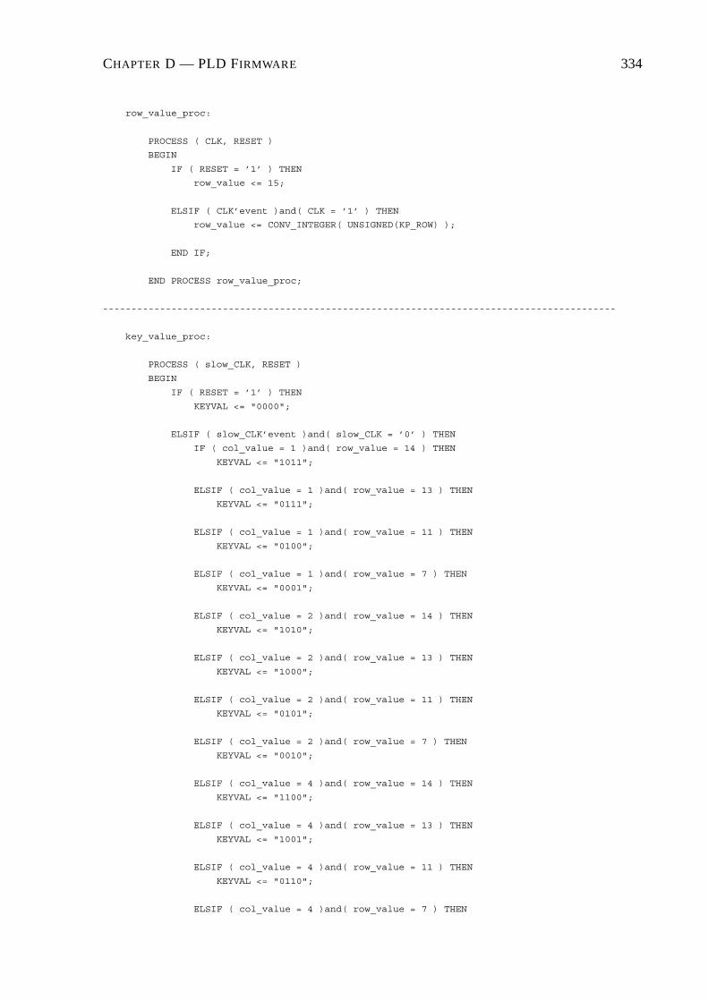
CHAPTER D — PLD FIRMWARE 334
row_value_proc:
PROCESS ( CLK, RESET )
BEGIN
IF ( RESET = ’1’ ) THEN
row_value <= 15;
ELSIF ( CLK’event )and( CLK = ’1’ ) THEN
row_value <= CONV_INTEGER( UNSIGNED(KP_ROW) );
END IF;
END PROCESS row_value_proc;
------------------------------------------------------------------------------------------
key_value_proc:
PROCESS ( slow_CLK, RESET )
BEGIN
IF ( RESET = ’1’ ) THEN
KEYVAL <= "0000";
ELSIF ( slow_CLK’event )and( slow_CLK = ’0’ ) THEN
IF ( col_value = 1 )and( row_value = 14 ) THEN
KEYVAL <= "1011";
ELSIF ( col_value = 1 )and( row_value = 13 ) THEN
KEYVAL <= "0111";
ELSIF ( col_value = 1 )and( row_value = 11 ) THEN
KEYVAL <= "0100";
ELSIF ( col_value = 1 )and( row_value = 7 ) THEN
KEYVAL <= "0001";
ELSIF ( col_value = 2 )and( row_value = 14 ) THEN
KEYVAL <= "1010";
ELSIF ( col_value = 2 )and( row_value = 13 ) THEN
KEYVAL <= "1000";
ELSIF ( col_value = 2 )and( row_value = 11 ) THEN
KEYVAL <= "0101";
ELSIF ( col_value = 2 )and( row_value = 7 ) THEN
KEYVAL <= "0010";
ELSIF ( col_value = 4 )and( row_value = 14 ) THEN
KEYVAL <= "1100";
ELSIF ( col_value = 4 )and( row_value = 13 ) THEN
KEYVAL <= "1001";
ELSIF ( col_value = 4 )and( row_value = 11 ) THEN
KEYVAL <= "0110";
ELSIF ( col_value = 4 )and( row_value = 7 ) THEN

CHAPTER D — PLD FIRMWARE 335
KEYVAL <= "0011";
END IF;
END IF;
END PROCESS key_value_proc;
------------------------------------------------------------------------------------------
slow_clk_proc:
PROCESS ( CLK, RESET )
BEGIN
IF ( RESET = ’1’ ) THEN
slow_clk_cntr <= 0;
slow_CLK <= ’0’;
ELSIF ( CLK’event )and( CLK = ’1’ ) THEN
IF ( slow_clk_cntr < 15 ) THEN
slow_clk_cntr <= slow_clk_cntr+1;
slow_clk <= slow_CLK;
ELSE
slow_clk_cntr <= 0;
slow_CLK <= not slow_CLK;
END IF;
END IF;
END PROCESS slow_clk_proc;
END a;

CHAPTER D — PLD FIRMWARE 336
D.3 Firmware for EPLD ExBus

CHAPTER D — PLD FIRMWARE 337
D.3.1 VHDL Code for the ExBus Single Complete Module of EPLD
ExBus-- PEC 33 - The complete expansion bus module 2002-11-07
LIBRARY ieee;
USE ieee.std_logic_1164.all;
USE ieee.std_logic_arith.all;
ENTITY EXBUS_Single_Complete IS
GENERIC (
n : INTEGER RANGE 0 TO 31 := 15
);
PORT (
EXBUS : INOUT STD_LOGIC_VECTOR( n DOWNTO 0 );
A_nEN : OUT STD_LOGIC;
nACK : IN STD_LOGIC;
D_nEN : OUT STD_LOGIC;
RnW : OUT STD_LOGIC;
nCS : IN STD_LOGIC;
RDYnBSY : OUT STD_LOGIC;
nINT : OUT STD_LOGIC;
nINTREQ_IN : IN STD_LOGIC;
nINTREQ_OUT : OUT STD_LOGIC;
DSP_RnW : IN STD_LOGIC;
DSP_nSTRB : IN STD_LOGIC;
DATA : INOUT STD_LOGIC_VECTOR( n DOWNTO 0 );
ADDR : IN STD_LOGIC_VECTOR( n DOWNTO 0 );
nRESET : IN STD_LOGIC;
CLK : IN STD_LOGIC
);
END EXBUS_Single_Complete;
ARCHITECTURE a OF EXBUS_Single_Complete IS
SIGNAL signal_DATA_IN : STD_LOGIC_VECTOR ( n DOWNTO 0 );
SIGNAL signal_DATA_OUT : STD_LOGIC_VECTOR ( n DOWNTO 0 );
SIGNAL signal_EXBUS_IN : STD_LOGIC_VECTOR ( n DOWNTO 0 );
SIGNAL signal_EXBUS_OUT : STD_LOGIC_VECTOR ( n DOWNTO 0 );
SIGNAL signal_EXBUS_RnW : STD_LOGIC;
SIGNAL signal_RDYnBSY : STD_LOGIC;
SIGNAL signal_RnW : STD_LOGIC;
SIGNAL signal_Data_Bidir_RnW : STD_LOGIC;
SIGNAL global_reset : STD_LOGIC;
COMPONENT ExBus_Ctrl
GENERIC (
n : INTEGER RANGE 0 TO 31 := 15

CHAPTER D — PLD FIRMWARE 338
);
PORT (
EXBUS_IN : IN STD_LOGIC_VECTOR( n DOWNTO 0 );
EXBUS_OUT : OUT STD_LOGIC_VECTOR( n DOWNTO 0 );
EXBUS_RnW : OUT STD_LOGIC;
A_nEN : OUT STD_LOGIC;
nACK : IN STD_LOGIC;
D_nEN : OUT STD_LOGIC;
RnW : OUT STD_LOGIC;
nCS : IN STD_LOGIC;
nINT : OUT STD_LOGIC;
RDYnBSY : OUT STD_LOGIC;
DSP_RnW : IN STD_LOGIC;
DSP_nSTRB : IN STD_LOGIC;
ADDR : IN STD_LOGIC_VECTOR( n DOWNTO 0 );
DATA_IN : IN STD_LOGIC_VECTOR( n DOWNTO 0 );
DATA_OUT : OUT STD_LOGIC_VECTOR( n DOWNTO 0 );
RESET : IN STD_LOGIC;
CLK : IN STD_LOGIC
);
END COMPONENT;
COMPONENT Bidir
GENERIC (
n : INTEGER RANGE 0 TO 31 := 15
);
PORT (
BIDIR : INOUT STD_LOGIC_VECTOR ( n DOWNTO 0 );
RnW : IN STD_LOGIC;
CLK : IN STD_LOGIC;
IN_DATA : IN STD_LOGIC_VECTOR ( n DOWNTO 0 );
OUT_DATA : OUT STD_LOGIC_VECTOR ( n DOWNTO 0 )
);
END COMPONENT;
BEGIN
global_reset <= not nRESET;
nINTREQ_OUT <= nINTREQ_IN;
RnW <= ’1’ WHEN ( signal_RDYnBSY = ’1’ ) ELSE signal_RnW;
RDYnBSY <= signal_RDYnBSY;
signal_Data_Bidir_RnW <= not DSP_RnW WHEN ( DSP_nSTRB = ’0’)and
( nCS = ’0’) ELSE ’1’;

CHAPTER D — PLD FIRMWARE 339
------------------------------------------------------------------------------------------
bidir_DataBus_map:
Bidir GENERIC MAP ( n => n )
PORT MAP( BIDIR => DATA, RnW => signal_Data_Bidir_RnW,
CLK => CLK, IN_DATA => signal_DATA_OUT,
OUT_DATA => signal_DATA_IN );
------------------------------------------------------------------------------------------
ExBus_map:
ExBus_Ctrl GENERIC MAP ( n => n )
PORT MAP(
EXBUS_IN => signal_EXBUS_IN,
EXBUS_OUT => signal_EXBUS_OUT,
EXBUS_RnW => signal_EXBUS_RnW,
A_nEN => A_nEN,
nACK => nACK,
D_nEN => D_nEN,
RnW => signal_RnW,
nCS => nCS,
nINT => nINT,
RDYnBSY => signal_RDYnBSY,
DSP_RnW => DSP_RnW,
DSP_nSTRB => DSP_nSTRB,
ADDR => ADDR,
DATA_IN => signal_DATA_IN,
DATA_OUT => signal_DATA_OUT,
RESET => global_reset,
CLK => CLK
);
------------------------------------------------------------------------------------------
bidir_ExBus_map:
Bidir GENERIC MAP ( n => n )
PORT MAP ( BIDIR => EXBUS, RnW => signal_EXBUS_RnW,
CLK => CLK, IN_DATA => signal_EXBUS_OUT,
OUT_DATA => signal_EXBUS_IN );
END a;

CHAPTER D — PLD FIRMWARE 340

CHAPTER D — PLD FIRMWARE 341
D.3.2 VHDL Code for the ExBus Ctrl Module of EPLD ExBus-- PEC 33 - Expansion Bus Component 2002-11-01
LIBRARY ieee;
USE ieee.std_logic_1164.all;
USE ieee.std_logic_arith.all;
ENTITY EXBUS_Ctrl IS
GENERIC (
n : INTEGER RANGE 0 TO 31 := 15
);
PORT (
EXBUS_IN : IN STD_LOGIC_VECTOR( n DOWNTO 0 );
EXBUS_OUT : OUT STD_LOGIC_VECTOR( n DOWNTO 0 );
EXBUS_RnW : OUT STD_LOGIC;
A_nEN : OUT STD_LOGIC;
nACK : IN STD_LOGIC;
D_nEN : OUT STD_LOGIC;
RnW : OUT STD_LOGIC; --Next transaction type
nCS : IN STD_LOGIC;
nINT : OUT STD_LOGIC;
RDYnBSY : OUT STD_LOGIC;
DSP_RnW : IN STD_LOGIC;
DSP_nSTRB : IN STD_LOGIC;
ADDR : IN STD_LOGIC_VECTOR( n DOWNTO 0 );
DATA_IN : IN STD_LOGIC_VECTOR( n DOWNTO 0 );
DATA_OUT : OUT STD_LOGIC_VECTOR( n DOWNTO 0 );
RESET : IN STD_LOGIC;
CLK : IN STD_LOGIC
);
END EXBUS_Ctrl;
ARCHITECTURE a OF EXBUS_Ctrl IS
TYPE state_type IS ( idle_state, addr_state, addr_ack_state, data_state,
data_ack_state, nint_state );
SIGNAL state : state_type;
SIGNAL next_state : state_type;
SIGNAL signal_DATA_OUT : STD_LOGIC_VECTOR ( n DOWNTO 0 );
SIGNAL signal_DATA_IN : STD_LOGIC_VECTOR ( n DOWNTO 0 );
SIGNAL signal_EXBUS_OUT : STD_LOGIC_VECTOR ( n DOWNTO 0 );
SIGNAL signal_EXBUS_IN : STD_LOGIC_VECTOR ( n DOWNTO 0 );
SIGNAL signal_WR_DATA : STD_LOGIC_VECTOR ( n DOWNTO 0 );
SIGNAL signal_RD_DATA : STD_LOGIC_VECTOR ( n DOWNTO 0 );
SIGNAL signal_ADDR : STD_LOGIC_VECTOR ( n DOWNTO 0 );

CHAPTER D — PLD FIRMWARE 342
-- RnW signal for Expansion Bus ( == NOT RnW for Data Bus )
SIGNAL signal_RnW : STD_LOGIC;
SIGNAL signal_RDYnBSY : STD_LOGIC;
SIGNAL clk_cntr : INTEGER RANGE 0 TO 15;
SIGNAL addr_ack_rec : STD_LOGIC;
SIGNAL data_ack_rec : STD_LOGIC;
SIGNAL start_trig : STD_LOGIC;
BEGIN
A_nEN <= ’0’ WHEN ( state = addr_state ) ELSE ’1’;
D_nEN <= ’0’ WHEN ( state = data_state ) ELSE ’1’;
nINT <= ’0’ WHEN ( state = nint_state ) ELSE ’1’;
RDYnBSY <= signal_RDYnBSY;
signal_RDYnBSY <= ’1’ WHEN ( state = idle_state ) ELSE ’0’;
DATA_OUT <= signal_DATA_OUT;
signal_DATA_IN <= DATA_IN;
signal_EXBUS_IN <= EXBUS_IN;
RnW <= signal_RnW;
------------------------------------------------------------------------------------------
EXBUS_RnW_proc:
PROCESS ( CLK, RESET )
BEGIN
IF ( RESET = ’1’ ) THEN
EXBUS_RnW <= ’1’;
ELSIF ( CLK’event )and( CLK = ’1’ ) THEN
IF ( state = idle_state ) THEN
EXBUS_RnW <= ’1’;
ELSIF ( state = addr_state)or( state = addr_ack_state ) THEN
EXBUS_RnW <= ’0’;
ELSE
EXBUS_RnW <= signal_RnW;
END IF;
END IF;
END PROCESS EXBUS_RnW_proc;
------------------------------------------------------------------------------------------
ADDR_proc:
PROCESS ( DSP_nSTRB, RESET )
BEGIN
IF ( RESET = ’1’ ) THEN
signal_ADDR <= ( others => ’0’ );
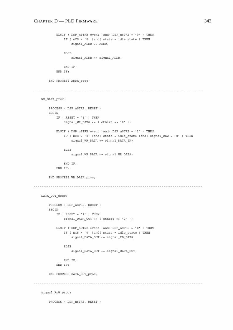
CHAPTER D — PLD FIRMWARE 343
ELSIF ( DSP_nSTRB’event )and( DSP_nSTRB = ’0’ ) THEN
IF ( nCS = ’0’ )and( state = idle_state ) THEN
signal_ADDR <= ADDR;
ELSE
signal_ADDR <= signal_ADDR;
END IF;
END IF;
END PROCESS ADDR_proc;
------------------------------------------------------------------------------------------
WR_DATA_proc:
PROCESS ( DSP_nSTRB, RESET )
BEGIN
IF ( RESET = ’1’ ) THEN
signal_WR_DATA <= ( others => ’0’ );
ELSIF ( DSP_nSTRB’event )and( DSP_nSTRB = ’1’ ) THEN
IF ( nCS = ’0’ )and( state = idle_state )and( signal_RnW = ’0’ ) THEN
signal_WR_DATA <= signal_DATA_IN;
ELSE
signal_WR_DATA <= signal_WR_DATA;
END IF;
END IF;
END PROCESS WR_DATA_proc;
------------------------------------------------------------------------------------------
DATA_OUT_proc:
PROCESS ( DSP_nSTRB, RESET )
BEGIN
IF ( RESET = ’1’ ) THEN
signal_DATA_OUT <= ( others => ’0’ );
ELSIF ( DSP_nSTRB’event )and( DSP_nSTRB = ’0’ ) THEN
IF ( nCS = ’0’ )and( state = idle_state ) THEN
signal_DATA_OUT <= signal_RD_DATA;
ELSE
signal_DATA_OUT <= signal_DATA_OUT;
END IF;
END IF;
END PROCESS DATA_OUT_proc;
------------------------------------------------------------------------------------------
signal_RnW_proc:
PROCESS ( DSP_nSTRB, RESET )

CHAPTER D — PLD FIRMWARE 344
BEGIN
IF ( RESET = ’1’ ) THEN
signal_RnW <= ’1’;
ELSIF ( DSP_nSTRB’event )and( DSP_nSTRB = ’0’ ) THEN
IF ( nCS = ’0’ )and( state = idle_state ) THEN
signal_RnW <= DSP_RnW;
ELSE
signal_RnW <= signal_RnW;
END IF;
END IF;
END PROCESS signal_RnW_proc;
------------------------------------------------------------------------------------------
EXBUS_OUT_proc:
PROCESS ( CLK, RESET )
BEGIN
IF ( RESET = ’1’ ) THEN
EXBUS_OUT <= ( others => ’0’ );
ELSIF ( CLK’event )and( CLK = ’1’ ) THEN
IF ( state = addr_state ) THEN
EXBUS_OUT <= signal_ADDR;
ELSIF ( state = data_state )or( state = data_ack_state ) THEN
EXBUS_OUT <= signal_WR_DATA;
END IF;
END IF;
END PROCESS EXBUS_OUT_proc;
------------------------------------------------------------------------------------------
EXBUS_IN_proc:
PROCESS ( nACK, RESET, state )
BEGIN
IF ( RESET = ’1’ ) THEN
signal_RD_DATA <= ( others => ’0’ );
ELSIF ( nACK’event )and( nACK = ’0’ ) THEN
IF ( ( state = data_ack_state )or( state = data_ack_state ) )and
( signal_RnW = ’1’ ) THEN
signal_RD_DATA <= signal_EXBUS_IN;
ELSE
signal_RD_DATA <= signal_RD_DATA;
END IF;
END IF;
END PROCESS EXBUS_IN_proc;

CHAPTER D — PLD FIRMWARE 345
------------------------------------------------------------------------------------------
addr_ack_proc:
PROCESS ( nACK, RESET )
BEGIN
IF ( RESET = ’1’ )or( state /= addr_ack_state ) THEN
addr_ack_rec <= ’0’;
ELSIF ( nACK’event )and( nACK = ’0’ ) THEN
addr_ack_rec <= ’1’;
END IF;
END PROCESS addr_ack_proc;
------------------------------------------------------------------------------------------
data_ack_proc:
PROCESS ( nACK, RESET )
BEGIN
IF ( RESET = ’1’ )or( state /= data_ack_state ) THEN
data_ack_rec <= ’0’;
ELSIF ( nACK’event )and( nACK = ’0’ ) THEN
data_ack_rec <= ’1’;
END IF;
END PROCESS data_ack_proc;
------------------------------------------------------------------------------------------
sm_proc:
PROCESS ( state )
BEGIN
CASE state IS
WHEN idle_state =>
next_state <= addr_state;
WHEN addr_state =>
next_state <= addr_ack_state;
WHEN addr_ack_state =>
IF ( addr_ack_rec = ’1’ ) THEN
next_state <= data_state;
ELSE
next_state <= idle_state;
END IF;
WHEN data_state =>
next_state <= data_ack_state;
WHEN data_ack_state =>
IF ( signal_RnW = ’1’ ) THEN
next_state <= nint_state;
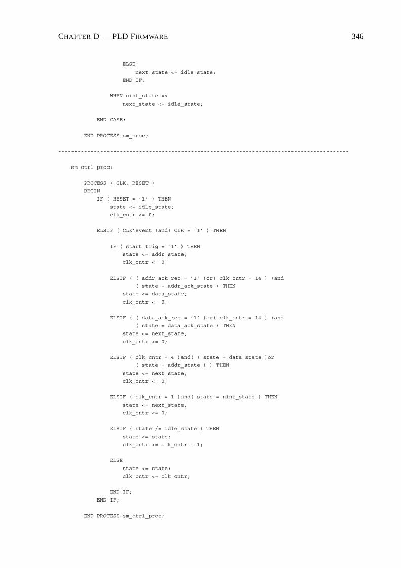
CHAPTER D — PLD FIRMWARE 346
ELSE
next_state <= idle_state;
END IF;
WHEN nint_state =>
next_state <= idle_state;
END CASE;
END PROCESS sm_proc;
------------------------------------------------------------------------------------------
sm_ctrl_proc:
PROCESS ( CLK, RESET )
BEGIN
IF ( RESET = ’1’ ) THEN
state <= idle_state;
clk_cntr <= 0;
ELSIF ( CLK’event )and( CLK = ’1’ ) THEN
IF ( start_trig = ’1’ ) THEN
state <= addr_state;
clk_cntr <= 0;
ELSIF ( ( addr_ack_rec = ’1’ )or( clk_cntr = 14 ) )and
( state = addr_ack_state ) THEN
state <= data_state;
clk_cntr <= 0;
ELSIF ( ( data_ack_rec = ’1’ )or( clk_cntr = 14 ) )and
( state = data_ack_state ) THEN
state <= next_state;
clk_cntr <= 0;
ELSIF ( clk_cntr = 4 )and( ( state = data_state )or
( state = addr_state ) ) THEN
state <= next_state;
clk_cntr <= 0;
ELSIF ( clk_cntr = 1 )and( state = nint_state ) THEN
state <= next_state;
clk_cntr <= 0;
ELSIF ( state /= idle_state ) THEN
state <= state;
clk_cntr <= clk_cntr + 1;
ELSE
state <= state;
clk_cntr <= clk_cntr;
END IF;
END IF;
END PROCESS sm_ctrl_proc;

CHAPTER D — PLD FIRMWARE 347
------------------------------------------------------------------------------------------
start_proc:
PROCESS ( DSP_nSTRB, RESET )
BEGIN
IF ( RESET = ’1’ )or( signal_RDYnBSY = ’0’ ) THEN
start_trig <= ’0’;
ELSIF ( DSP_nSTRB’event )and( DSP_nSTRB = ’1’ ) THEN
IF ( nCS = ’0’ ) THEN
start_trig <= ’1’;
END IF;
END IF;
END PROCESS start_proc;
END a;

CHAPTER D — PLD FIRMWARE 348
D.3.3 VHDL Code for the BiDir Module of EPLD ExBus-- Bidirectional Bus 2002-11-07
LIBRARY ieee;
USE ieee.std_logic_1164.all;
USE ieee.std_logic_arith.all;
-- -------------------------------------------------------------------
-- | RnW | BIDIR | IN_DATA | OUT_DATA |
-- -------------------------------------------------------------------
-- -------------------------------------------------------------------
-- | 1 | ZZZZZZZZZZZZZZZZ | XXXXXXXXXXXXXXXX | BIDIR |
-- -------------------------------------------------------------------
-- | 0 | IN_DATA | Data | BIDIR |
-- -------------------------------------------------------------------
ENTITY Bidir IS
GENERIC (
n : INTEGER RANGE 0 TO 31 := 15
);
PORT (
BIDIR : INOUT STD_LOGIC_VECTOR ( n DOWNTO 0 );
RnW : IN STD_LOGIC;
CLK : IN STD_LOGIC;
IN_DATA : IN STD_LOGIC_VECTOR ( n DOWNTO 0 );
OUT_DATA : OUT STD_LOGIC_VECTOR ( n DOWNTO 0 )
);
END Bidir;
ARCHITECTURE maxpld OF Bidir IS
SIGNAL a : STD_LOGIC_VECTOR ( n DOWNTO 0 );
SIGNAL b : STD_LOGIC_VECTOR ( n DOWNTO 0 );
BEGIN
PROCESS ( CLK )
BEGIN
IF ( CLK’event )and( CLK = ’0’ ) THEN
a <= IN_DATA;
OUT_DATA <= b;
END IF;
END PROCESS;
PROCESS ( RnW, BIDIR )
BEGIN
IF ( RnW = ’1’ ) THEN
BIDIR <= ( others => ’Z’ );
b <= BIDIR;
ELSE
BIDIR <= a;

CHAPTER D — PLD FIRMWARE 349
b <= BIDIR;
END IF;
END PROCESS;
END maxpld;

Appendix A
Schematics
A.1 Schematics of the PEC33
120

CHAPTER A — SCHEMATICS 121
Figure A.1: Schematic of the DSP and Flash RAM of the PEC33 Controller
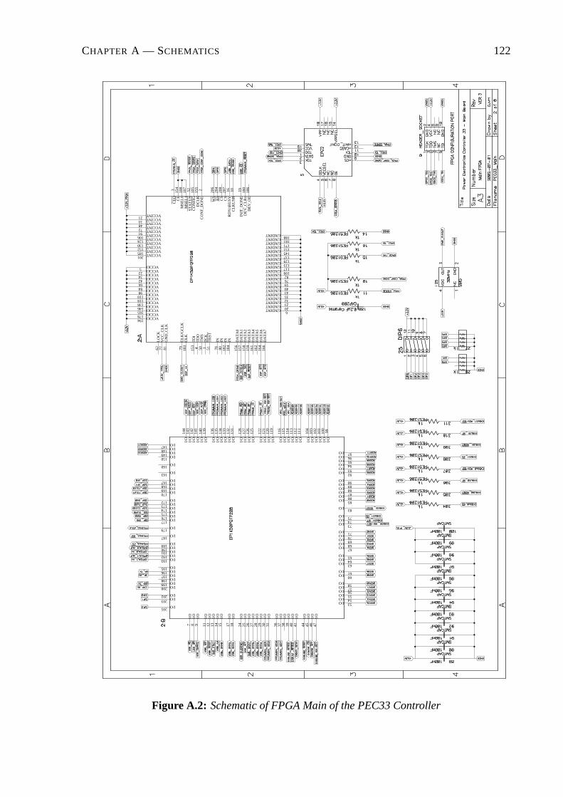
CHAPTER A — SCHEMATICS 122
97I/O96I/O
90I/O89I/O88I/O87I/O86I/O85I/O
83I/O
93I/O92I/O
95I/O94I/O
111
I/O
99I/O
104
I/O10
3I/O
102
I/O10
1I/O
100
I/O
58I/O57I/O56I/O55I/O
44I/O
45I/O
47I/O
46I/O
60I/O 61I/O63I/O 64I/O 65I/O
68I/O67I/O69I/O 70I/O 71I/O73I/O 74I/O 75I/O
54I/O53I/O
24I/O
28I/O
27I/O
26I/O
25I/O
17I/O
18I/O
15I/O
14I/O
13I/O
12I/O
11I/O
9I/O
8I/O
7I/O
187 I/O
189 I/O
179 I/O177 I/O175 I/O176 I/O
144
I/O
141
I/O14
2I/O
143
I/O
139
I/O14
0I/O
131
I/O13
2I/O
133
I/O13
4I/O
135
I/O13
6I/O
125
I/O12
6I/O
127
I/O12
8I/O
163 I/O160 I/O150 I/O
147 I/O148 I/O149 I/O
174 I/O173 I/O172 I/O170 I/O
167 I/O168 I/O169 I/O
120
I/O12
1I/O
122
I/O30
I/O31
I/O
29I/O
40I/O
41I/O
37I/O
38I/O
39I/O
36I/O
112
I/O11
3I/O
119
I/O
114
I/O11
5I/O
116
I/O
205 I/O203 I/O202 I/O
200 I/O
198 I/O199 I/O
196 I/O197 I/O
195 I/O
193 I/O192 I/O190 I/O191 I/O
166
DA
TA7
164
DA
TA6
162
DA
TA5
6GNDINT 20GNDINT 23GNDINT 32GNDINT 35GNDINT 43GNDINT 49GNDINT 59GNDINT 76GNDINT 82GNDINT 109GNDINT 117GNDINT 123GNDINT 129GNDINT 137GNDINT 145GNDINT 151GNDINT 171GNDINT188GNDINT181GNDINT
80IN
78IN
50TM
S4
TDO
184
IN
183
CLK
182
IN
161
DA
TA4
159
DA
TA3
158
DA
TA2
157
DA
TA1
156
DA
TA0
153
TDI
1TC
K
77V
CC
_CLK
81G
ND
_CLK
84 VCCIO98 VCCIO
194 VCCIO165 VCCIO
110 VCCIO118 VCCIO138 VCCIO146 VCCIO
178 VCCIO
66 VCCIO42 VCCIO34 VCCIO22 VCCIO5 VCCIO
91 VCCINT106 VCCINT
130 VCCINT
185 VCCINT
124 VCCINT
152 VCCINT
201 VCCINT
21 VCCINT
48 VCCINT33 VCCINT
72 VCCINT
62LO
CK
79C
LK/G
CLK
51TR
ST
207
CS
2C
ON
F_D
ON
E
19IN
IT_D
ON
E
186
DEV
_OE
180
DEV
_CLR
n
16R
DY
nBU
SY
155
DC
LK
10C
LKU
SR
108
MSE
L010
7M
SEL1
206
WS
208
CS
204
RS
105
CO
NFI
G52
STA
TUS
154
CE
3C
EO
Figure A.2: Schematic of FPGA Main of the PEC33 Controller
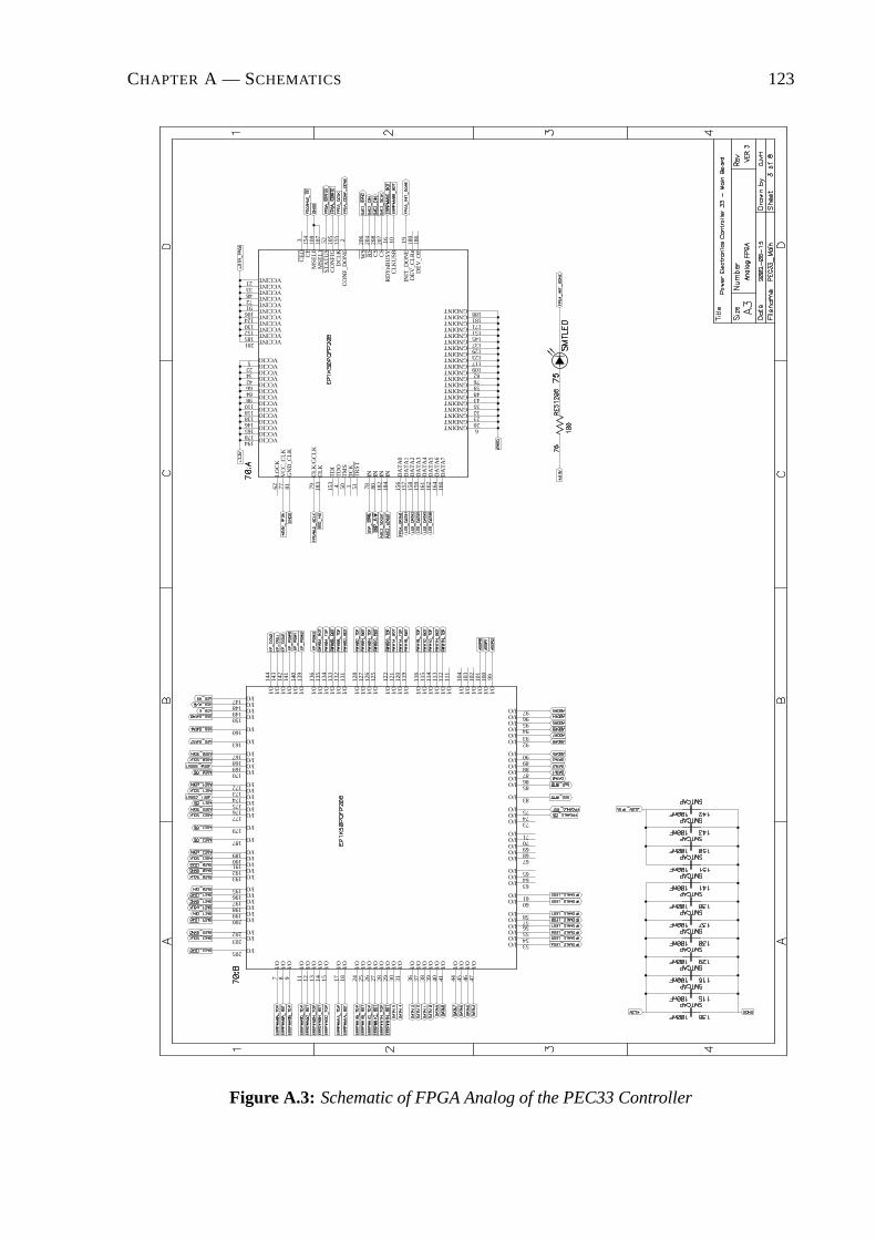
CHAPTER A — SCHEMATICS 123
97I/O96I/O
90I/O89I/O88I/O87I/O86I/O85I/O
83I/O
93I/O92I/O
95I/O94I/O
111
I/O
99I/O
104
I/O10
3I/O
102
I/O10
1I/O
100
I/O
58I/O57I/O56I/O55I/O
44I/O
45I/O
47I/O
46I/O
60I/O 61I/O63I/O 64I/O 65I/O
68I/O67I/O69I/O 70I/O 71I/O73I/O 74I/O 75I/O
54I/O53I/O
24I/O
28I/O
27I/O
26I/O
25I/O
17I/O
18I/O
15I/O
14I/O
13I/O
12I/O
11I/O
9I/O
8I/O
7I/O
187 I/O
189 I/O
179 I/O177 I/O175 I/O176 I/O
144
I/O
141
I/O14
2I/O
143
I/O
139
I/O14
0I/O
131
I/O13
2I/O
133
I/O13
4I/O
135
I/O13
6I/O
125
I/O12
6I/O
127
I/O12
8I/O
163 I/O160 I/O150 I/O
147 I/O148 I/O149 I/O
174 I/O173 I/O172 I/O170 I/O
167 I/O168 I/O169 I/O
120
I/O12
1I/O
122
I/O30
I/O31
I/O
29I/O
40I/O
41I/O
37I/O
38I/O
39I/O
36I/O
112
I/O11
3I/O
119
I/O
114
I/O11
5I/O
116
I/O
205 I/O203 I/O202 I/O
200 I/O
198 I/O199 I/O
196 I/O197 I/O
195 I/O
193 I/O192 I/O190 I/O191 I/O
166
DA
TA7
164
DA
TA6
162
DA
TA5
6GNDINT 20GNDINT 23GNDINT 32GNDINT 35GNDINT 43GNDINT 49GNDINT 59GNDINT 76GNDINT 82GNDINT 109GNDINT 117GNDINT 123GNDINT 129GNDINT 137GNDINT 145GNDINT 151GNDINT 171GNDINT188GNDINT181GNDINT
80IN
78IN
50TM
S4
TDO
184
IN
183
CLK
182
IN
161
DA
TA4
159
DA
TA3
158
DA
TA2
157
DA
TA1
156
DA
TA0
153
TDI
1TC
K
77V
CC
_CLK
81G
ND
_CLK
84 VCCIO98 VCCIO
194 VCCIO165 VCCIO
110 VCCIO118 VCCIO138 VCCIO146 VCCIO
178 VCCIO
66 VCCIO42 VCCIO34 VCCIO22 VCCIO5 VCCIO
91 VCCINT106 VCCINT
130 VCCINT
185 VCCINT
124 VCCINT
152 VCCINT
201 VCCINT
21 VCCINT
48 VCCINT33 VCCINT
72 VCCINT
62LO
CK
79C
LK/G
CLK
51TR
ST
207
CS
2C
ON
F_D
ON
E
19IN
IT_D
ON
E
186
DEV
_OE
180
DEV
_CLR
n
16R
DY
nBU
SY
155
DC
LK
10C
LKU
SR
108
MSE
L010
7M
SEL1
206
WS
208
CS
204
RS
105
CO
NFI
G52
STA
TUS
154
CE
3C
EO
Figure A.3: Schematic of FPGA Analog of the PEC33 Controller

CHAPTER A — SCHEMATICS 124
Figure A.4: Schematic of the Ports and Drivers of the PEC33 Controller
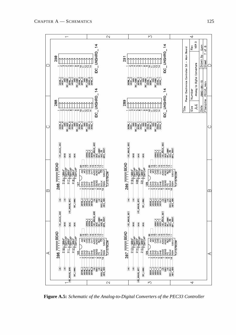
CHAPTER A — SCHEMATICS 125
Figure A.5: Schematic of the Analog-to-Digital Converters of the PEC33 Controller

CHAPTER A — SCHEMATICS 126
Figure A.6: Schematic of the Digital-to-Analog Converters of the PEC33 Controller

CHAPTER A — SCHEMATICS 127
86GNDINT38GNDINT
95GNDIO74GNDIO59GNDIO43GNDIO26GNDIO11GNDIO
91 VCCINT39 VCCINT
51 VCCIO266 VCCIO282 VCCIO2
34 VCCIO118 VCCIO13 VCCIO1
87IN
PUT/
GC
LK1
88IN
PUT/
OE1
89IN
PUT/
GC
LRn
90IN
PUT/
OE2
/GC
LK2
73TD
O15
TMS
4TD
I
62TC
K
12V
REF
A60
VR
EFB
17I/O
19I/O
20I/O
21I/O
22I/O
23I/O
24I/O
25I/O
16I/O
27I/O 28I/O 29I/O 30I/O 31I/O 32I/O 33I/O35I/O 36I/O 37I/O
42I/O41I/O40I/O
48I/O47I/O46I/O45I/O44I/O
50I/O49I/O
52I/O
53I/O
54I/O
55I/O
56I/O
57I/O
58I/O
61I/O
1I/O
2I/O
5I/O
6I/O
7I/O
8I/O
9I/O
10I/O
13I/O
14I/O
63I/O
64I/O
65I/O
67I/O
68I/O
69I/O
70I/O
71I/O
72I/O
75I/O
99 I/O100 I/O
96 I/O97 I/O98 I/O
92 I/O93 I/O94 I/O
83 I/O84 I/O85 I/O
76 I/O77 I/O78 I/O79 I/O80 I/O81 I/O
86GNDINT38GNDINT
95GNDIO74GNDIO59GNDIO43GNDIO26GNDIO11GNDIO
91 VCCINT39 VCCINT
51 VCCIO266 VCCIO282 VCCIO2
34 VCCIO118 VCCIO13 VCCIO1
87IN
PUT/
GC
LK1
88IN
PUT/
OE1
89IN
PUT/
GC
LRn
90IN
PUT/
OE2
/GC
LK2
73TD
O15
TMS
4TD
I
62TC
K
12V
REF
A60
VR
EFB
17I/O
19I/O
20I/O
21I/O
22I/O
23I/O
24I/O
25I/O
16I/O
27I/O 28I/O 29I/O 30I/O 31I/O 32I/O 33I/O35I/O 36I/O 37I/O
42I/O41I/O40I/O
48I/O47I/O46I/O45I/O44I/O
50I/O49I/O
52I/O
53I/O
54I/O
55I/O
56I/O
57I/O
58I/O
61I/O
1I/O
2I/O
5I/O
6I/O
7I/O
8I/O
9I/O
10I/O
13I/O
14I/O
63I/O
64I/O
65I/O
67I/O
68I/O
69I/O
70I/O
71I/O
72I/O
75I/O
99 I/O100 I/O
96 I/O97 I/O98 I/O
92 I/O93 I/O94 I/O
83 I/O84 I/O85 I/O
76 I/O77 I/O78 I/O79 I/O80 I/O81 I/O
Figure A.7: Schematic of EPLD ExBus and the Expansion ports of the PEC33 Controller

CHAPTER A — SCHEMATICS 128
Figure A.8: Schematic of the Power Supply and Reset Circuitry of the PEC33 Controller

CHAPTER A — SCHEMATICS 129
A.2 Schematics of the PEC33 Optical Fibre Expansion
Board

CHAPTER A — SCHEMATICS 130
Figure A.9: Schematic of the Optical Fibre Transmitters of the PEC33 Expansion Board

CHAPTER A — SCHEMATICS 131
Figure A.10: Schematic of the Optical Fibre Receivers of the PEC33 Expansion Board

CHAPTER A — SCHEMATICS 132
A.3 Schematics of the Voltage and Current Probes

CHAPTER A — SCHEMATICS 133
Figure A.11: Schematic of the Voltage Probes

CHAPTER A — SCHEMATICS 134
Figure A.12: Schematic of the Current Probes

Appendix B
Printed Circuit Board Layouts
B.1 Printed Circuit Board Layout of the PEC33
135
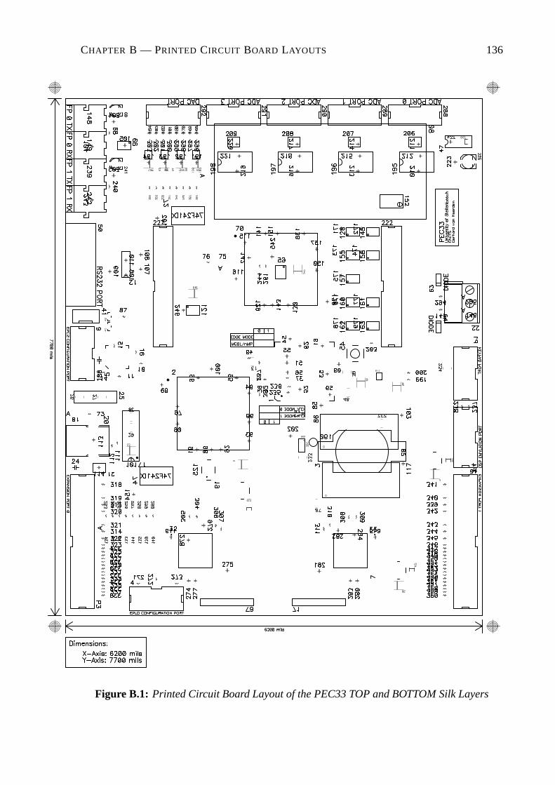
CHAPTER B — PRINTED CIRCUIT BOARD LAYOUTS 136
Figure B.1: Printed Circuit Board Layout of the PEC33 TOP and BOTTOM Silk Layers

CHAPTER B — PRINTED CIRCUIT BOARD LAYOUTS 137
Figure B.2: Printed Circuit Board Layout of the PEC33 TOP Layer

CHAPTER B — PRINTED CIRCUIT BOARD LAYOUTS 138
Figure B.3: Printed Circuit Board Layout of the PEC33 BOTTOM Layer

CHAPTER B — PRINTED CIRCUIT BOARD LAYOUTS 139
Figure B.4: Printed Circuit Board Layout of the PEC33 POWER Layer

CHAPTER B — PRINTED CIRCUIT BOARD LAYOUTS 140
Figure B.5: Printed Circuit Board Layout of the PEC33 Ground Layer

CHAPTER B — PRINTED CIRCUIT BOARD LAYOUTS 141
B.2 Printed Circuit Board Layout of the PEC33 Optical
Fibre Expansion Board
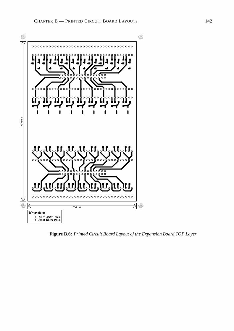
CHAPTER B — PRINTED CIRCUIT BOARD LAYOUTS 142
Figure B.6: Printed Circuit Board Layout of the Expansion Board TOP Layer

CHAPTER B — PRINTED CIRCUIT BOARD LAYOUTS 143
Figure B.7: Printed Circuit Board Layout of the Expansion Board BOT Layer

CHAPTER B — PRINTED CIRCUIT BOARD LAYOUTS 144
B.3 Printed Circuit Board Layout of the Voltage and
Current Probes

CHAPTER B — PRINTED CIRCUIT BOARD LAYOUTS 145
Figure B.8: Printed Circuit Board Layout of the Current and Voltage Probes TOP and
BOTTOM Silk Layers

CHAPTER B — PRINTED CIRCUIT BOARD LAYOUTS 146
Figure B.9: Printed Circuit Board Layout of the Current and Voltage Probes TOP Layers

CHAPTER B — PRINTED CIRCUIT BOARD LAYOUTS 147
Figure B.10: Printed Circuit Board Layout of the Current and Voltage Probes BOTTOM
Layers

Appendix C
DSP C Example Programs
148

CHAPTER C — DSP C EXAMPLE PROGRAMS 149
C.1 The Header File Containing the Address Definitions,
PEC33 Address.h
/* Header file containing register address declarations and constant definitions */
/* DSP Main constant definitions */
/* Serie port */
#define global_ctrl 0
#define tx_ctrl 2
#define rx_ctrl 3
#define timer_ctrl 4
#define timer_cntr 5
#define timer_period 6
#define tx_data 8
#define rx_data 0xC
/* DSP register address declarations */
volatile int *serie0 = (int *) 0x808040;
/* FPGA Main constant definitions */
#define rtc_status 0
#define rtc_wr_addr 1
/* FPGA Main register address declarations */
volatile int *RS232Port=(int *) 0x500000;
volatile int *fram_reg=(int *) 0x500008;
volatile int *rtc=(int *) 0x500010;
volatile int *rtc_wr_data=(int *) 0x500012;
volatile int *rtc_rd_data=(int *) 0x500013;
volatile int *main_cmd0=(int *) 0x500066;
volatile int *main_cmd1=(int *) 0x500067;
/* FRAM constant definitions */
#define TX_Data 0
#define RX_Data 1
#define Status 2
#define BaudRate 3
#define fram_status 0
/* FRAM register address declarations */
volatile int *fram0=(int *) 0x400000;
volatile int *fram1=(int *) 0xC00000;
/* FPGA Analog constant definitions */
/* DAC registers */
#define ctrl_addr 0

CHAPTER C — DSP C EXAMPLE PROGRAMS 150
#define a_conf_addr 1
#define a_data_addr 2
#define b_conf_addr 3
#define b_data_addr 4
/* ADC Registers */
#define adc_conf_addr 0
#define adc_data_addr 1
#define adc_samp_chan0_addr 2
#define adc_samp_chan1_addr 3
#define adc_samp_chan2_addr 4
#define adc_samp_chan3_addr 5
#define adc_samp_chan4_addr 6
#define adc_samp_chan5_addr 7
#define adc_samp_chan6_addr 8
#define adc_samp_chan7_addr 9
/* LCD Registers */
#define mode_addr 0
#define char_addr 1
#define addr_addr 2
#define status_addr 3
/* PWM Registers */
#define pwm_refa_addr 0
#define pwm_refb_addr 1
#define pwm_refc_addr 2
#define pwm_refn_addr 3
#define pwm_trimax_addr 4
#define pwm_trifreqscale_addr 5
#define pwm_deadtime_addr 6
#define pwm_upval_addr 7
#define pwm_downval_addr 8
#define dac0_load_cmd 1 /* 00000001b */
#define dac1_load_cmd 2 /* 00000010b */
#define dac2_load_cmd 4 /* 00000100b */
#define dac3_load_cmd 8 /* 00001000b */
#define lcd_updatemode_cmd 16 /* 00010000b */
#define lcd_updatedata_cmd 32 /* 00100000b */
#define lcd_reset_cmd 64 /* 01000000b */
#define adc0_en_cmd 1 /* 00000001b */
#define adc1_en_cmd 2 /* 00000010b */
#define adc2_en_cmd 4 /* 00000100b */
#define adc3_en_cmd 8 /* 00001000b */
#define pwm0_en_cmd 16 /* 00010000b */
#define pwm1_en_cmd 32 /* 00100000b */
/* FPGA Analog register address declarations */
volatile int *dac0=(int *) 0x600000;
volatile int *dac1=(int *) 0x600008;
volatile int *dac2=(int *) 0x600010;
volatile int *dac3=(int *) 0x600018;
volatile int *adc_status=(int *) 0x600020;
/*Register to show which adc have new data ready --- 4 Bits

CHAPTER C — DSP C EXAMPLE PROGRAMS 151
||---------||---------||---------||---------||
|| 3 || 2 || 1 || 0 ||
|| ADC3 || ADC2 || ADC1 || ADC0 ||
|| Ready || Ready || Ready || Ready ||
||---------||---------||---------||---------|| */
volatile int *adc0=(int *) 0x600021;
volatile int *adc1=(int *) 0x60002B;
volatile int *adc2=(int *) 0x600035;
volatile int *adc3=(int *) 0x60003F;
volatile int *lcd=(int *) 0x600049;
volatile int *pwm_status=(int *) 0x60004D;
volatile int *pwm0=(int *) 0x60004E;
volatile int *pwm1=(int *) 0x600057;
volatile int *pwm_err_top=(int *) 0x600060;
volatile int *pwm_err_bot=(int *) 0x600061;
volatile int *fpganlg_int_en=(int *) 0x600062;
/*Register to enable the different interrupt sources --- 15 Bits
||---------||---------||---------||---------||---------||---------||---------||---------||
|| 14 || 13 || 12 || 11 || 10 || 9 || 8 || 7 ||
|| PWM1 || PWM1 || PWM1 || PWM1 || PWM0 || PWM0 || PWM0 || PWM0 ||
|| Counter || Ramp || Compare || Compare || Counter || Ramp || Compare || Compare ||
|| Zero || Dir || Down || Up || Zero || Dir || Down || Up ||
||---------||---------||---------||---------||---------||---------||---------||---------||
|| 6 || 5 || 4 || 3 || 2 || 1 || 0 ||
|| PWM || PWM || Keypad || adc3 || adc2 || adc1 || adc0 ||
|| Error || Error || || || || || ||
|| Bot || Top || || || || || ||
||---------||---------||---------||---------||---------||---------||---------||*/
volatile int *keyval=(int *) 0x600063;
volatile int *fpganlg_int_reg=(int *) 0x600065;
/*Register show which entity caused interrupt --- 6 Bits
||---------||---------||---------||---------||---------||---------||
|| 5 || 4 || 3 || 2 || 1 || 0 ||
|| PWM1 || PWM0 || PWM || PWM || Keypad || adc ||
|| status || status || Error || Error || || ||
|| || || Bot || Top || || ||
||---------||---------||---------||---------||---------||---------|| */
volatile int *analog_cmd0=(int *) 0x600066;
volatile int *analog_cmd1=(int *) 0x600067;
unsigned int *int2_addr=(unsigned int *) 0x809FC3;

CHAPTER C — DSP C EXAMPLE PROGRAMS 152
C.2 The DSP C Program to Copy Serial Input Data to
FRAM 0, SERIAL2FRAM.c/* This program copies data received with the DSP’s serial
port to sector 0 of FRAM 0, the address where the DSP
loads its program from when it boots from FRAM 0.
*/
#include <string.h>
#include <math.h>
#include <stdlib.h>
#include <float.h>
#include <limits.h>
#include "Address2.h"
#define pi (double)3.14159265359
#define mask10 1023
asm(" .sect \"vectors\" ");
asm(" NOP ");
asm(" NOP ");
asm(" NOP ");
asm(" NOP ");
asm(" NOP ");
asm(" BU _intR ");
unsigned int addr;
unsigned int data;
unsigned int rx_arr[4096];
unsigned int arr_cntr;
unsigned int downloadStarted;
unsigned int downloadCounter;
void analog_doCmd0( int cmd )
{
*analog_cmd0 = cmd;
*analog_cmd0 = 0;
}
void analog_doCmd1( int cmd )
{
*analog_cmd1 = cmd;
}
void myDelay( int cntr )
{
int i_cntr;
i_cntr = 0;
while ( i_cntr < cntr ) {
i_cntr++;
}

CHAPTER C — DSP C EXAMPLE PROGRAMS 153
}
/* Procedure that erases the data of sector, sect_addr, of FRAM 0 */
void eraseSector ( unsigned int sect_addr )
{
int addr;
int status;
if ( sect_addr > 6 ) exit;
/* Determine the sector address */
switch ( sect_addr )
{
case 0:
addr = 0;
break;
case 1:
addr = 2*0x08000;
break;
case 2:
addr = 2*0x10000;
break;
case 3:
addr = 2*0x18000;
break;
case 4:
addr = 2*0x1C000;
break;
case 5:
addr = 2*0x1D000;
break;
case 6:
addr = 2*0x1E000;
break;
default:
break;
}
/* Wait until FRAM 0 is ready */
status = fram_reg[fram_status]&1;
while ( status == 0 ) {
myDelay(100);
status = fram_reg[fram_status]&1;
}
/* Output erase command sequence */
fram0[0xAAA] = (unsigned int)(0xAA);
fram0[0x555] = (unsigned int)(0x55);
fram0[0xAAA] = (unsigned int)(0x80);
fram0[0xAAA] = (unsigned int)(0xAA);
fram0[0x555] = (unsigned int)(0x55);
fram0[addr] = (unsigned int)(0x30);
myDelay( 7000 );
}
/* Procedure that writes a byte, data, to address, addr, in FRAM 0 */
void writeByte ( unsigned int addr, unsigned int data )
{

CHAPTER C — DSP C EXAMPLE PROGRAMS 154
int status;
/* Wait until FRAM 0 is ready */
status = fram_reg[fram_status]&1;
while ( status == 0 ) {
myDelay(100);
status = fram_reg[fram_status]&1;
}
/* Output write command sequence */
fram0[0xAAA] = (unsigned int)(0xAA);
fram0[0x555] = (unsigned int)(0x55);
fram0[0xAAA] = (unsigned int)(0xA0);
fram0[addr] = (unsigned int)(data);
}
/* Procedure that reads data from FRAM 0 */
void readByte ( unsigned int addr )
{
int status;
/* Wait until FRAM 0 is ready */
status = fram_reg[fram_status]&1;
while ( status == 0 ) {
myDelay(100);
status = fram_reg[fram_status]&1;
}
/* Read data from FRAM 0 */
data = fram0[addr]&65535;
}
/* Serial reception interrupt routine */
interrupt void intR(void)
{
unsigned int data, data0, data1, data2, data3;
asm(" AND 00h,IE");
asm(" AND 0FFFFFFDFh,IF");
/* Set flag indicating that the program data is being transferred to the DSP */
downloadStarted = 1;
/* Counter is reset everytime serial data is received.
This counter/flag isused to test if the downloading had finished, by
asuming that when this counter reaches 10000000, the last word had been
received.
*/
downloadCounter = 0;
/* Read the received data word from the DSP serial receive register */
data = serie0[rx_data];
/* Break the word up into bytes */
data0 = ((data>>16)>>8);
data1 = (data>>16)&0xFF;
data2 = (data>>8)&0xFF;
data3 = data&0xFF;
CHAPTER C — DSP C EXAMPLE PROGRAMS 155
/* Store the received bytes in the receive array, rx_arr */
if ( arr_cntr < 4096 ) {
rx_arr[arr_cntr] = data3;
rx_arr[arr_cntr+1] = data2;
rx_arr[arr_cntr+2] = data1;
rx_arr[arr_cntr+3] = data0;
arr_cntr = arr_cntr+4;
}
asm(" OR 20h,IE");
asm(" OR 2000h,ST");
}
main(void)
{
unsigned int i,j;
unsigned int dummy;
unsigned int out_data;
unsigned int status;
unsigned int *prim_bus_ctrl = (unsigned int *)0x808064;
*prim_bus_ctrl = 0x10C8;
asm(" OR 00h,IE"); /*asm(" OR 20h,IE"); */
asm(" OR 0000h,ST");
downloadStarted = 0;
downloadCounter = 0;
arr_cntr = 0;
i = 0;
while (i<4096) {
rx_arr[i] = 0x00000000;
i++;
}
serie0[global_ctrl] = 0x0EB00044;
serie0[tx_ctrl] = 0x00000333;
serie0[rx_ctrl] = 0x00000111;
serie0[timer_ctrl] = 0x000001CF;
serie0[timer_cntr] = 0x00;
serie0[timer_period] = 0x00010001;
RS232Port[BaudRate] = 3;
asm(" OR 20h,IE");
asm(" OR 2000h,ST");
/* Wait for download to start */
downloadStarted = 0;
while (downloadStarted == 0)
{
}
/* Wait for download to finish -- counter is reset each time data is received */

CHAPTER C — DSP C EXAMPLE PROGRAMS 156
downloadCounter = 0;
while ( downloadCounter < 10000000 )
{
downloadCounter++;
}
asm(" OR 00h,IE");
/* Erase sector 0 of FRAM 0 */
eraseSector( 0 );
/* Write the program data to FRAM 0 */
i = 0;
while (i < arr_cntr)
{
out_data = rx_arr[i];
writeByte ( i, out_data);
i++;
}
while ( 1 ) {
}
}
CHAPTER C — DSP C EXAMPLE PROGRAMS 157
C.3 The DSP C Program to Test the Liquid Crystal Display,
LCD Test1.c/* LCD test program
It seems that the first character written to the
LCD is lost, therefore first write a dummy character.
*/
#include <string.h>
#include <math.h>
#include <stdlib.h>
#include <float.h>
#include <limits.h>
#include "PEC33_Address.h"
#define pi (double)3.14159265359
#define mask10 1023
asm(" .sect \"vectors\" ");
asm(" NOP ");
asm(" NOP ");
asm(" NOP ");
int pos;
void analog_doCmd0( int cmd )
{
*analog_cmd0 = cmd;
*analog_cmd0 = 0;
}
void analog_doCmd1( int cmd )
{
*analog_cmd1 = cmd;
}
void Mode( int mode, int delay )
{
int status;
status = 0;
/* Copy LCD mode data to FPGA Analog */
lcd[mode_addr] = mode;
/* Check if LCD is ready -- status = 1 */
status = lcd[status_addr]&1;
while ( status == 0 ) {
status = lcd[status_addr]&1;
}
/* Update the LCD mode */

CHAPTER C — DSP C EXAMPLE PROGRAMS 158
analog_doCmd0(lcd_updatemode_cmd);
/* Execute delay */
status = 0;
while ( status < delay ) {
status++;
}
}
void DisplayChar( int lcdaddr, char lcddata, int delay )
{
int status;
status = 0;
/* Copy LCD character data to FPGA Analog */
lcd[char_addr] = lcddata;
/* Copy LCD address data to FPGA Analog */
lcd[addr_addr] = lcdaddr;
/* Check if LCD is ready -- status = 1 */
status = lcd[status_addr]&1;
while ( status == 0 ) {
status = lcd[status_addr]&1;
}
/* Update the LCD */
analog_doCmd0(lcd_updatedata_cmd);
/* Execute delay */
status = 0;
while ( status < delay ) {
status++;
}
}
main(void)
{
int i;
unsigned int *prim_bus_ctrl = (unsigned int *)0x808064;
*prim_bus_ctrl = 0x10F8;
/* Disable interrupts */
asm(" OR 0h,IE");
asm(" OR 2000h,ST");
i = 0;
while (i<13000000) {
i++;
}
/* Initialize the LCD */
Mode( 0x30, 300000 );
Mode( 0x30, 10000 );
Mode( 0x30, 0 );

CHAPTER C — DSP C EXAMPLE PROGRAMS 159
Mode( 0x3C, 0 );
Mode( 0x0C, 0 );
Mode( 0x01, 0 );
Mode( 0x06, 0 );
i = 0;
while (i<1500000) {
i++;
}
DisplayChar( 0, ’ ’, 0 ); /* dummy character */
DisplayChar( 0, ’H’, 0 );
DisplayChar( 1, ’A’, 0 );
DisplayChar( 2, ’L’, 0 );
DisplayChar( 3, ’L’, 0 );
DisplayChar( 4, ’O’, 0 );
DisplayChar( 5, ’ ’, 0 );
DisplayChar( 6, ’W’, 0 );
DisplayChar( 7, ’O’, 0 );
DisplayChar( 8, ’R’, 0 );
DisplayChar( 9, ’L’, 0 );
DisplayChar( 10, ’D’, 0 );
DisplayChar( 11, ’!’, 0 );
DisplayChar( 64, ’L’, 0 );
DisplayChar( 65, ’i’, 0 );
DisplayChar( 66, ’n’, 0 );
DisplayChar( 67, ’e’, 0 );
DisplayChar( 68, ’ ’, 0 );
DisplayChar( 69, ’2’, 30000000 );
while ( 1 ) {
pos = 0;
while ( pos < 18 ) {
DisplayChar( pos-2, ’ ’, 0 ); /* dummy character */
DisplayChar( pos-2, ’-’, 0 );
DisplayChar( pos-1, ’=’, 0 );
DisplayChar( pos, ’>’, 2000000 );
pos++;
}
while ( pos > 0 ) {
DisplayChar( pos, ’ ’, 0 ); /* dummy character */
DisplayChar( pos, ’<’, 0 );
DisplayChar( pos+1, ’=’, 0 );
DisplayChar( pos+2, ’-’, 2000000 );

CHAPTER C — DSP C EXAMPLE PROGRAMS 160
pos--;
}
}
}
CHAPTER C — DSP C EXAMPLE PROGRAMS 161
C.4 The DSP C Program to Test the Real-Time Clock,
RTC Test.c
#include <string.h>
#include <math.h>
#include <stdlib.h>
#include <float.h>
#include <limits.h>
#include "PEC33_Address.h"
#define pi (double)3.14159265359
#define mask10 1023
asm(" .sect \"vectors\" ");
asm(" NOP ");
asm(" NOP ");
asm(" NOP ");
int j;
int hr, min, sec, time;
int ls_sec, ms_sec;
int ls_min, ms_min;
int ls_hr, ms_hr;
void main_doCmd0( int cmd )
{
*main_cmd0 = cmd;
*main_cmd0 = 0;
}
void main_doCmd1( int cmd )
{
*main_cmd1 = cmd;
}
void analog_doCmd0( int cmd )
{
*analog_cmd0 = cmd;
*analog_cmd0 = 0;
}
void analog_doCmd1( int cmd )
{
*analog_cmd1 = cmd;
}
void Mode( int mode, int delay )
{
int status;
status = 0;
/* Copy LCD mode data to FPGA Analog */
lcd[mode_addr] = mode;

CHAPTER C — DSP C EXAMPLE PROGRAMS 162
/* Check if LCD is ready -- status = 1 */
status = lcd[status_addr]&1;
while ( status == 0 ) {
status = lcd[status_addr]&1;
}
/* Update the LCD mode */
analog_doCmd0(lcd_updatemode_cmd);
/* Execute delay */
status = 0;
while ( status < delay ) {
status++;
}
}
void DisplayInt( int lcdaddr, int lcddata, int delay )
{
int status;
status = 0;
/* Copy LCD character data to FPGA Analog */
lcd[char_addr] = lcddata;
/* Copy LCD address data to FPGA Analog */
lcd[addr_addr] = lcdaddr;
/* Check if LCD is ready -- status = 1 */
status = lcd[status_addr]&1;
while ( status == 0 ) {
status = lcd[status_addr]&1;
}
/* Update the LCD */
analog_doCmd0(lcd_updatedata_cmd);
/* Execute delay */
status = 0;
while ( status < delay ) {
status++;
}
}
void DisplayChar( int lcdaddr, char lcddata, int delay )
{
int status;
status = 0;
/* Copy LCD character data to FPGA Analog */
lcd[char_addr] = lcddata;
/* Copy LCD address data to FPGA Analog */
lcd[addr_addr] = lcdaddr;
/* Check if LCD is ready -- status = 1 */
status = lcd[status_addr]&1;
while ( status == 0 ) {
status = lcd[status_addr]&1;

CHAPTER C — DSP C EXAMPLE PROGRAMS 163
}
/* Update the LCD */
analog_doCmd0(lcd_updatedata_cmd);
/* Execute delay */
status = 0;
while ( status < delay ) {
status++;
}
}
void RTC_Write_Data( int addr, int data )
{
int delay;
int status;
/* Check if RTC is ready -- status = 1 */
status = rtc[rtc_status]&1;
while ( status != 1 ) {
status = rtc[rtc_status]&1;
}
/* Copy RTC data to FPGA Main */
*rtc_wr_data = data;
/* Copy address of RTC data to FPGA Main */
rtc[rtc_wr_addr] = addr;
/* Update RTC data */
main_doCmd0( 1 );
}
int RTC_Read_Data( int addr )
{
int data;
int status;
/* Check if RTC is ready -- status = 1 */
status = rtc[rtc_status]&1;
while ( status != 1 ) {
status = rtc[rtc_status]&1;
/*status++;*/
}
/* Get most recent RTC data from FPGA Main */
if ( ( addr <= 7 )&&( addr >= 0 ) ) {
data = rtc_rd_data[ addr ]&255;
}
else {
data = -1;
}
/* Return the data */
return data;
}

CHAPTER C — DSP C EXAMPLE PROGRAMS 164
main(void)
{
int i,j;
int pos;
unsigned int *prim_bus_ctrl = (unsigned int *)0x808064;
*prim_bus_ctrl = 0x10C8;
/* Disable interrupts */
asm(" OR 0h,IE");
asm(" OR 2000h,ST");
i = 0;
while (i<11250000) {
i++;
}
/* Initialize the LCD */
Mode( 0x30, 3075000 );
Mode( 0x30, 750000 );
Mode( 0x30, 0 );
Mode( 0x3C, 0 );
Mode( 0x0C, 0 );
Mode( 0x01, 0 );
Mode( 0x06, 0 );
i = 0;
while (i<150000) {
i++;
}
/* Output ’HALLO WORLD!’ on LCD */
DisplayChar( 0, ’ ’, 0 ); /* dummy character */
DisplayChar( 0, ’H’, 0 );
DisplayChar( 1, ’A’, 0 );
DisplayChar( 2, ’L’, 0 );
DisplayChar( 3, ’L’, 0 );
DisplayChar( 4, ’O’, 0 );
DisplayChar( 5, ’ ’, 0 );
DisplayChar( 6, ’W’, 0 );
DisplayChar( 7, ’O’, 0 );
DisplayChar( 8, ’R’, 0 );
DisplayChar( 9, ’L’, 0 );
DisplayChar( 10, ’D’, 0 );

CHAPTER C — DSP C EXAMPLE PROGRAMS 165
DisplayChar( 11, ’!’, 30000000 );
/* Clear the LCD */
Mode( 0x01, 0 );
/* Set RTC seconds = 30 */
RTC_Write_Data( 0, 0x30 );
/* Enable RTC square wave output ( 1Hz ) */
RTC_Write_Data( 7, 0x10 );
/* Set RTC minutes = 59 */
RTC_Write_Data( 1, 0x59 );
/* Set RTC hours = 23 */
RTC_Write_Data( 2, 0x23 );
/* Set RTC day = 7 */
RTC_Write_Data( 3, 0x07 );
/* Set RTC date = 31 */
RTC_Write_Data( 4, 0x31 );
/* Set RTC month = 12 */
RTC_Write_Data( 5, 0x12 );
/* Set RTC year = 99 */
RTC_Write_Data( 6, 0x99 );
j = 0;
while ( 1 ) {
/* Wait before updating LCD */
i = 0;
while (i<100000) {
i++;
}
/* Read the hours */
hr = RTC_Read_Data( 2 );
/* Read the minutes */
min = RTC_Read_Data( 1 );
/* Read the seconds */
sec = RTC_Read_Data( 0 );
ls_hr = (hr&0x0F) + 0x30;
ms_hr = ((hr&0x30)>>4) + 0x30 ;
ls_min = (min&0x0F) + 0x30;
ms_min = ((min&0x70)>>4) + 0x30;
ls_sec = (sec&0x0F) + 0x30;
ms_sec = ((sec&0x70)>>4) + 0x30;
DisplayChar( 0x00, ’ ’, 0x00 ); /* dummy character */
DisplayInt( 0x00, ms_hr, 0x00 );
DisplayInt( 0x01, ls_hr, 0x00 );

CHAPTER C — DSP C EXAMPLE PROGRAMS 166
DisplayInt( 0x03, ms_min, 0x00 );
DisplayInt( 0x04, ls_min, 0x00 );
DisplayInt( 0x06, ms_sec, 0x00 );
DisplayInt( 0x07, ls_sec, 0x00 );
}
}
C.5 The DSP C Program Implementing the Active Power
Filter’s Control Algorithm#include <string.h>
#include <math.h>
#include <stdlib.h>
#include <float.h>
#include <limits.h>
#include "Address2.h"
asm(" .sect \"vectors\" ");
asm(" BU _int0 ");
asm(" NOP ");
asm(" BU _int2 ");
#define p_limit 50
#define trimax 750
float pi = 3.141592654;
float pos_tan60 = 1.73205;
float neg_tan60 = -1.73205;
float inv_Vd = 0.005;
float L = 0.002;
float Ts = 0.0002;
unsigned int probe;
unsigned int sector;
float Delta;
float invDelta;
float LdivTs;
float Iconv_Alfa_Ref, Iconv_Beta_Ref;
float V_Alfa_Ref, V_Beta_Ref;
float p, p_ac, p_tot, q, p_mean;
float V_A, V_B, V_C;
float I_A, I_B, I_C;
float Iconv_A, Iconv_B, Iconv_C;

CHAPTER C — DSP C EXAMPLE PROGRAMS 167
float V_Alfa, V_Beta;
float I_Alfa, I_Beta;
float Iconv_Alfa, Iconv_Beta;
float D_A, D_B, D_C;
float Ref_A, Ref_B, Ref_C;
unsigned int state;
unsigned int data_rdy;
unsigned int compute_new_refs;
unsigned int update_refs;
unsigned int cmd1_mask;
unsigned int adc0_data, adc0_chan;
unsigned int adc1_data, adc1_chan;
unsigned int adc2_data, adc2_chan;
unsigned int adc0_data0, adc0_data1, adc0_data2;
unsigned int adc1_data0, adc1_data1, adc1_data2;
unsigned int adc2_data0, adc2_data1, adc2_data2;
int offset_adc0_data0, offset_adc0_data1, offset_adc0_data2;
int offset_adc1_data0, offset_adc1_data1, offset_adc1_data2;
int offset_adc2_data0, offset_adc2_data1, offset_adc2_data2;
void doCmd0( int cmd )
{
int i;
*analog_cmd0 = cmd;
i = 0;
while ( i < 1 ) i++;
*analog_cmd0 = 0;
}
void doCmd1( int cmd )
{
int i;
*analog_cmd1 = cmd;
i = 0;
while ( i < 1 ) i++;
}
void ClarkeTransform( float Phase_A, float Phase_B, float Phase_C,
float *Alfa, float *Beta )
{
*Alfa = 0.816497*(Phase_A - 0.5*Phase_B - 0.5*Phase_C);
*Beta = 0.816497*(0.866025*Phase_B - 0.866025*Phase_C);
}
void InvClarkeTransform( float Alfa, float Beta, float *Phase_A,
float *Phase_B, float *Phase_C )
{
*Phase_A = 0.816497*(Alfa);
*Phase_B = 0.816497*(-0.5*Alfa + 0.866025*Beta);
*Phase_C = 0.816497*(-0.5*Alfa - 0.866025*Beta);
}

CHAPTER C — DSP C EXAMPLE PROGRAMS 168
unsigned int ComputeSector( float U_Alfa_Ref, float U_Beta_Ref )
{
int CS_sector;
if ( U_Beta_Ref >= 0.0 )
{
if ( U_Beta_Ref >= pos_tan60*abs(U_Alfa_Ref) )
{
CS_sector = 2;
}
else
if ( U_Alfa_Ref >= 0.0 )
{
CS_sector = 1;
}
else CS_sector = 3;
}
else
if ( U_Beta_Ref <= neg_tan60*abs(U_Alfa_Ref) )
{
CS_sector = 5;
}
else
if ( U_Alfa_Ref >= 0.0 )
{
CS_sector = 6;
}
else CS_sector = 4;
return CS_sector;
}
void ComputeDutyCycles( int CDS_sector, float U_Alfa_Ref, float U_Beta_Ref,
float *D_A, float *D_B, float *D_C )
{
float d1_, d2_, d3_, d4_, d5_, d6_;
float d0, d1, d2, d3, d4, d5, d6;
probe = 0;
if ( CDS_sector == 1 )
{
d1_ = inv_Vd*(1.225*U_Alfa_Ref - 0.7071*U_Beta_Ref);
d2_ = inv_Vd*( 1.414*U_Beta_Ref);
if ( d1_ + d2_ < 1.0 )
{
d1 = d1_;
d2 = d2_;
d0 = 1.0 - (d1_ + d2_);
}
else
{
d1 = d1_/(d1_+d2_);
d2 = 1.0 - d1;
d0 = 0.0;
}

CHAPTER C — DSP C EXAMPLE PROGRAMS 169
*D_A = 0.5*d0 + d1 + d2;
*D_B = 0.5*d0 + d2;
*D_C = 0.5*d0;
probe = 1;
}
else if ( CDS_sector == 2 )
{
d2_ = inv_Vd*(1.225*U_Alfa_Ref + 0.7071*U_Beta_Ref);
d3_ = inv_Vd*(-1.225*U_Alfa_Ref + 0.7071*U_Beta_Ref);
if ( d2_ + d3_ < 1.0 )
{
d2 = d2_;
d3 = d3_;
d0 = 1.0 - (d2_ + d3_);
}
else
{
d2 = d2_/(d2_+d3_);
d3 = 1.0 - d2;
d0 = 0.0;
}
*D_A = 0.5*d0 + d2;
*D_B = 0.5*d0 + d2 + d3;
*D_C = 0.5*d0;
probe = 2;
}
else if ( CDS_sector == 3 )
{
d3_ = inv_Vd*( 1.414*U_Beta_Ref);
d4_ = inv_Vd*(-1.225*U_Alfa_Ref - 0.7071*U_Beta_Ref);
if ( d3_ + d4_ < 1.0 )
{
d3 = d3_;
d4 = d4_;
d0 = 1.0 - (d3_ + d4_);
}
else
{
d3 = d3_/(d3_+d4_);
d4 = 1.0 - d3;
d0 = 0.0;
}
*D_A = 0.5*d0;
*D_B = 0.5*d0 + d3 + d4;
*D_C = 0.5*d0 + d4;
probe = 3;
}
else if ( CDS_sector == 4 )
{
d4_ = inv_Vd*(-1.225*U_Alfa_Ref + 0.7071*U_Beta_Ref);
d5_ = inv_Vd*(-1.414*U_Beta_Ref);

CHAPTER C — DSP C EXAMPLE PROGRAMS 170
if ( d4_ + d5_ < 1.0 )
{
d4 = d4_;
d5 = d5_;
d0 = 1.0 - (d4_ + d5_);
}
else
{
d4 = d4_/(d4_+d5_);
d5 = 1.0 - d4;
d0 = 0.0;
}
*D_A = 0.5*d0;
*D_B = 0.5*d0 + d4;
*D_C = 0.5*d0 + d4 + d5;
probe = 4;
}
else if ( CDS_sector == 5 )
{
d5_ = inv_Vd*(-1.225*U_Alfa_Ref - 0.7071*U_Beta_Ref);
d6_ = inv_Vd*( 1.225*U_Alfa_Ref - 0.7071*U_Beta_Ref);
if ( d5_ + d6_ < 1.0 )
{
d5 = d5_;
d6 = d6_;
d0 = 1.0 - (d5_ + d6_);
}
else
{
d5 = d5_/(d5_+d6_);
d6 = 1.0 - d5;
d0 = 0.0;
}
*D_A = 0.5*d0 + d6;
*D_B = 0.5*d0;
*D_C = 0.5*d0 + d5 + d6;
probe = 5;
}
else if ( CDS_sector == 6 )
{
d6_ = inv_Vd*(-1.414*U_Beta_Ref);
d1_ = inv_Vd*( 1.225*U_Alfa_Ref + 0.7071*U_Beta_Ref);
if ( d6_ + d1_ < 1.0 )
{
d6 = d6_;
d1 = d1_;
d0 = 1.0 - (d6_ + d1_);
}
else
{
d6 = d6_/(d6_+d1_);
d1 = 1.0 - d6;

CHAPTER C — DSP C EXAMPLE PROGRAMS 171
d0 = 0.0;
}
*D_A = 0.5*d0 + d6 + d1;
*D_B = 0.5*d0;
*D_C = 0.5*d0 + d6;
probe = 6;
}
}
void Mode( int mode, int delay )
{
int status;
status = 0;
lcd[mode_addr] = mode;
while ( status < 1000000 ) {
status++;
}
doCmd0(lcd_updatemode_cmd);
status = 0;
while ( status < delay ) {
status++;
}
}
void Display( int lcdaddr, int lcddata, int delay )
{
int status;
status = 0;
lcd[char_addr] = lcddata;
lcd[addr_addr] = lcdaddr;
while ( status < 5000 ) {
status++;
}
doCmd0(lcd_updatedata_cmd);
status = 0;
while ( status < 5000 ) {
status++;
}
doCmd0(lcd_updatedata_cmd);
status = 0;
while ( status < delay ) {
status++;
}
}
interrupt void int2(void)
{
/* unsigned int keypressed;*/

CHAPTER C — DSP C EXAMPLE PROGRAMS 172
unsigned int int_reg;
asm(" AND 0h,IE");
asm(" AND 0FFFFFFFBh,IF");
dac0[b_data_addr] = 2048;
doCmd0( dac0_load_cmd );
int_reg = (*fpganlg_int_reg)&63;
asm(" OR 1h,IE");
asm(" AND 0FFFFFFFBh,IF");
}
interrupt void int0(void)
{
/*unsigned int adc_data, adc_chan; */
unsigned int int_reg;
unsigned int adc_status_reg;
unsigned int keypressed;
unsigned int temp0;
unsigned int temp1;
unsigned int temp2;
unsigned int temp_cntr;
asm(" AND 0h,IE");
asm(" AND 0FFFFFFFEh,IF");
int_reg = (*fpganlg_int_reg)&63;
if ((int_reg&16)==16) /* PWM block 0 event occured ? */
{
if (state == 0)
{
compute_new_refs = 1;
}
else if ( state == 2 )
{
update_refs = 1;
}
*fpganlg_int_en = 0x0007;
}
if ((int_reg&2)==2) /* A key was pressed ? */
{
keypressed = (unsigned int)((*keyval)&15);
if ( keypressed == 10 ) {
keypressed = keypressed + 0x26;
}
else if ( keypressed == 11 ) {
keypressed = keypressed + 0x1F;
}
else if ( keypressed == 12 ) {
keypressed = keypressed + 0x17;
}
else keypressed = keypressed + 0x30;

CHAPTER C — DSP C EXAMPLE PROGRAMS 173
Display( 0x0D, keypressed, 0x00 );
*fpganlg_int_en = 0x0007;
}
if ((int_reg&1)==1)
{
*fpganlg_int_en = 0x0000;
temp0 = (unsigned int)((adc0[adc_data_addr])&8191);
temp1 = (unsigned int)((adc1[adc_data_addr])&8191);
temp2 = (unsigned int)((adc2[adc_data_addr])&8191);
adc0_data = (unsigned int)( temp0&1023 );
adc0_chan = (unsigned int)( (temp0&7168) >> 10 );
adc1_data = (unsigned int)( temp1&1023 );
adc1_chan = (unsigned int)( (temp1&7168) >> 10 );
adc2_data = (unsigned int)( temp2&1023 );
adc2_chan = (unsigned int)( (temp2&7168) >> 10 );
if (adc0_chan==0)
{
adc0_data0 = adc0_data;
}
else
{
if (adc0_chan==1)
{
adc0_data1 = adc0_data;
}
else
{
if (adc0_chan==2)
{
adc0_data2 = adc0_data;
}
}
}
if (adc1_chan==0)
{
adc1_data0 = adc1_data;
}
else
{
if (adc1_chan==1)
{
adc1_data1 = adc1_data;
}
else
{
if (adc1_chan==2)
{
adc1_data2 = adc1_data;
}
}

CHAPTER C — DSP C EXAMPLE PROGRAMS 174
}
if (adc2_chan==0)
{
adc2_data0 = adc2_data;
}
else
{
if (adc2_chan==1)
{
adc2_data1 = adc2_data;
}
else
{
if (adc2_chan==2)
{
adc2_data2 = adc2_data;
}
}
}
*fpganlg_int_en = 0x0107;
}
asm(" OR 1h,IE");
asm(" AND 0FFFFFFFEh,IF");
}
main(void)
{
unsigned int pwmstatus;
int i,j,k,l;
int pos, dir;
unsigned int toggle;
float old_Iconv_A, old_Iconv_B, old_Iconv_C;
float delta_Iconv;
float q_old;
int p_num;
float p_arr[p_limit];
unsigned int *prim_bus_ctrl = (unsigned int *)0x808064;
*prim_bus_ctrl = 0x10F8;
*fpganlg_int_en = 0x0000;
LdivTs = L/Ts;
Ts = 0.0002;
toggle = 0;

CHAPTER C — DSP C EXAMPLE PROGRAMS 175
cmd1_mask = 0;
data_rdy = 0;
compute_new_refs = 0;
asm(" OR 1h,IE");
asm(" OR 2000h,ST");
asm(" AND 0FFFFFFFEh,IF");
adc0[adc_samp_chan0_addr] = 0;
adc0[adc_samp_chan1_addr] = 1;
adc0[adc_samp_chan2_addr] = 2;
adc0[adc_samp_chan3_addr] = 1;
adc0[adc_samp_chan4_addr] = 0;
adc0[adc_samp_chan5_addr] = 1;
adc0[adc_samp_chan6_addr] = 2;
adc0[adc_samp_chan7_addr] = 1;
adc1[adc_samp_chan0_addr] = 0;
adc1[adc_samp_chan1_addr] = 1;
adc1[adc_samp_chan2_addr] = 2;
adc1[adc_samp_chan3_addr] = 1;
adc1[adc_samp_chan4_addr] = 0;
adc1[adc_samp_chan5_addr] = 1;
adc1[adc_samp_chan6_addr] = 2;
adc1[adc_samp_chan7_addr] = 1;
adc2[adc_samp_chan0_addr] = 0;
adc2[adc_samp_chan1_addr] = 1;
adc2[adc_samp_chan2_addr] = 2;
adc2[adc_samp_chan3_addr] = 1;
adc2[adc_samp_chan4_addr] = 0;
adc2[adc_samp_chan5_addr] = 1;
adc2[adc_samp_chan6_addr] = 2;
adc2[adc_samp_chan7_addr] = 1;
adc0[adc_conf_addr] = 0x0000;
adc1[adc_conf_addr] = 0x0000;
adc2[adc_conf_addr] = 0x0000;
pwm0[pwm_trimax_addr] = trimax;
pwm0[pwm_trifreqscale_addr] = 1;
pwm0[pwm_deadtime_addr] = 60;
pwm0[pwm_upval_addr] = 1023;
pwm0[pwm_downval_addr] = 120;
pwm0[pwm_refa_addr] = trimax/2;
pwm0[pwm_refb_addr] = trimax/2;
pwm0[pwm_refc_addr] = trimax/2;
pwm0[pwm_refn_addr] = trimax/2;
dac0[ctrl_addr] = 3;
dac0[a_conf_addr] = 4;
dac0[b_conf_addr] = 4;
i = 0;
while (i<11250000) {
i++;

CHAPTER C — DSP C EXAMPLE PROGRAMS 176
}
Mode( 0x30, 3075000 );
Mode( 0x30, 750000 );
Mode( 0x30, 0 );
Mode( 0x3C, 0 );
Mode( 0x0C, 0 );
Mode( 0x01, 0 );
Mode( 0x06, 0 );
Display( 0x00, 0xFF, 0x00 );
i = 0;
while (i<150000) {
i++;
}
/* Display "HALLO WORLD!" on LCD */
Display( 0x00, 0x48, 0x00 );
Display( 0x01, 0x61, 0x00 );
Display( 0x02, 0x6C, 0x00 );
Display( 0x03, 0x6C, 0x00 );
Display( 0x04, 0x6F, 0x00 );
Display( 0x05, 0x20, 0x00 );
Display( 0x06, 0x57, 0x00 );
Display( 0x07, 0x6F, 0x00 );
Display( 0x08, 0x72, 0x00 );
Display( 0x09, 0x6C, 0x00 );
Display( 0x0A, 0x64, 0x00 );
Display( 0x0B, 0x21, 0x00 );
p_num = 0;
p_tot = 0.0;
while (p_num < p_limit)
{
p_arr[p_num] = 0.0;
++p_num;
}
p_num = 0;
adc0_data0 = 0;
adc0_data1 = 0;
adc0_data2 = 0;
adc1_data0 = 0;
adc1_data1 = 0;
adc1_data2 = 0;
adc2_data0 = 0;
adc2_data1 = 0;
adc2_data2 = 0;
offset_adc0_data0 = 0;
offset_adc0_data1 = 0;
offset_adc0_data2 = 0;
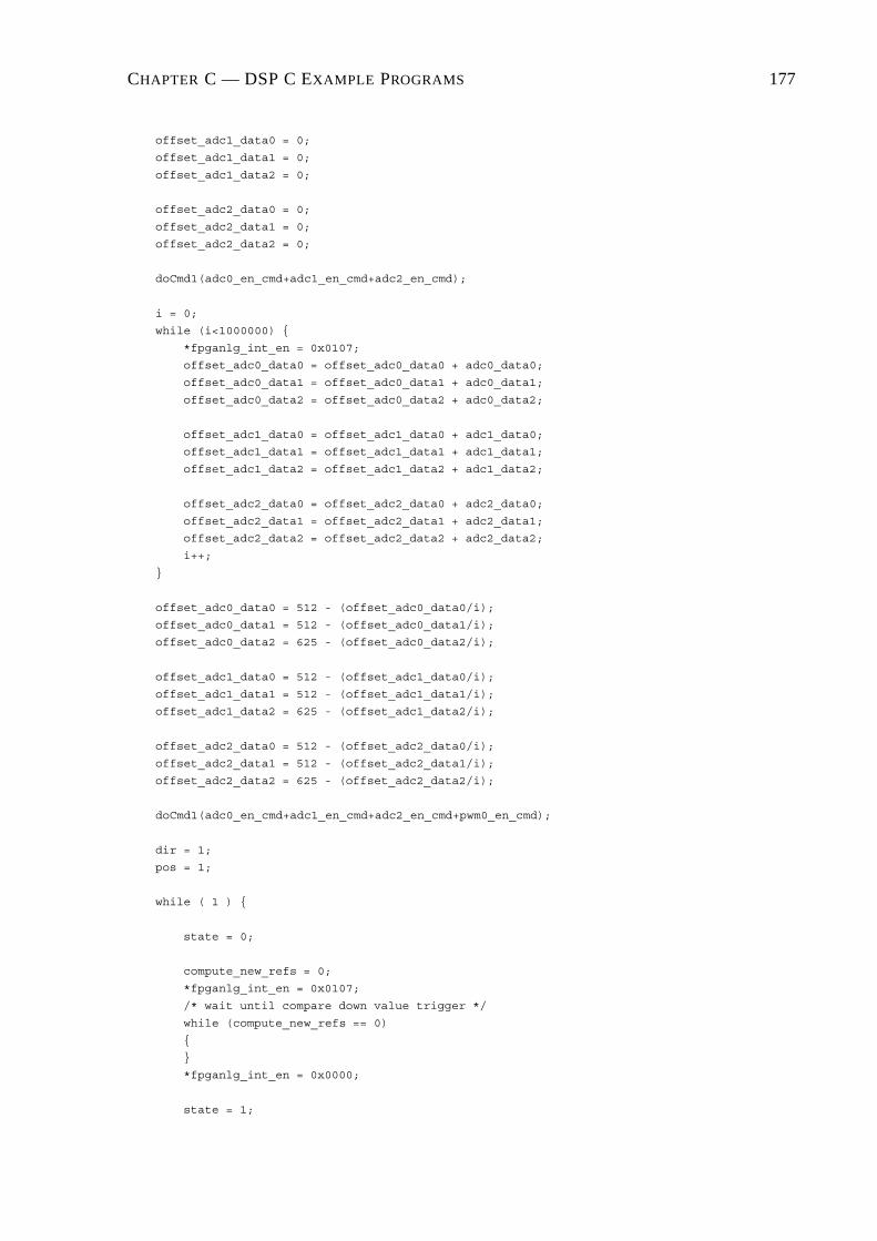
CHAPTER C — DSP C EXAMPLE PROGRAMS 177
offset_adc1_data0 = 0;
offset_adc1_data1 = 0;
offset_adc1_data2 = 0;
offset_adc2_data0 = 0;
offset_adc2_data1 = 0;
offset_adc2_data2 = 0;
doCmd1(adc0_en_cmd+adc1_en_cmd+adc2_en_cmd);
i = 0;
while (i<1000000) {
*fpganlg_int_en = 0x0107;
offset_adc0_data0 = offset_adc0_data0 + adc0_data0;
offset_adc0_data1 = offset_adc0_data1 + adc0_data1;
offset_adc0_data2 = offset_adc0_data2 + adc0_data2;
offset_adc1_data0 = offset_adc1_data0 + adc1_data0;
offset_adc1_data1 = offset_adc1_data1 + adc1_data1;
offset_adc1_data2 = offset_adc1_data2 + adc1_data2;
offset_adc2_data0 = offset_adc2_data0 + adc2_data0;
offset_adc2_data1 = offset_adc2_data1 + adc2_data1;
offset_adc2_data2 = offset_adc2_data2 + adc2_data2;
i++;
}
offset_adc0_data0 = 512 - (offset_adc0_data0/i);
offset_adc0_data1 = 512 - (offset_adc0_data1/i);
offset_adc0_data2 = 625 - (offset_adc0_data2/i);
offset_adc1_data0 = 512 - (offset_adc1_data0/i);
offset_adc1_data1 = 512 - (offset_adc1_data1/i);
offset_adc1_data2 = 625 - (offset_adc1_data2/i);
offset_adc2_data0 = 512 - (offset_adc2_data0/i);
offset_adc2_data1 = 512 - (offset_adc2_data1/i);
offset_adc2_data2 = 625 - (offset_adc2_data2/i);
doCmd1(adc0_en_cmd+adc1_en_cmd+adc2_en_cmd+pwm0_en_cmd);
dir = 1;
pos = 1;
while ( 1 ) {
state = 0;
compute_new_refs = 0;
*fpganlg_int_en = 0x0107;
/* wait until compare down value trigger */
while (compute_new_refs == 0)
{
}
*fpganlg_int_en = 0x0000;
state = 1;

CHAPTER C — DSP C EXAMPLE PROGRAMS 178
asm(" AND 0h,IE");
asm(" AND 0FFFFFFFEh,IF");
V_A = (float)(-0.3125*(float)(adc0_data0+offset_adc0_data0) + 160.0);
V_B = (float)(-0.3125*(float)(adc1_data0+offset_adc1_data0) + 160.0);
V_C = (float)(-0.3125*(float)(adc2_data0+offset_adc2_data0) + 160.0);
I_A = (float)(-0.019531*(float)(adc0_data1+offset_adc0_data1) + 10.0);
I_B = (float)(-0.019531*(float)(adc1_data1+offset_adc1_data1) + 10.0);
I_C = (float)(-0.019531*(float)(adc2_data1+offset_adc2_data1) + 10.0);
Iconv_A = (float)(0.0533*(float)(adc0_data2+offset_adc0_data2) - 33.3);
Iconv_B = (float)(0.0533*(float)(adc1_data2+offset_adc1_data2) - 33.3);
Iconv_C = (float)(0.0533*(float)(adc2_data2+offset_adc2_data2) - 33.3);
ClarkeTransform( V_A, V_B, V_C, &V_Alfa, &V_Beta );
ClarkeTransform( I_A, I_B, I_C, &I_Alfa, &I_Beta );
ClarkeTransform( Iconv_A, Iconv_B, Iconv_C, &Iconv_Alfa, &Iconv_Beta );
p = (float)(I_Alfa*V_Alfa + I_Beta*V_Beta);
q = (float)(-I_Alfa*V_Beta + I_Beta*V_Alfa);
/* Create circular buffer of power values to compute average power */
p_tot = p_tot - p_arr[p_num]; /* Subtract oldest value from sum of power values */
p_arr[p_num] = p; /* Insert the new value in the array */
p_tot = p_tot + p; /* Add new value to the value for the total power */
p_mean = p_tot/p_limit; /* Compute the average power */
p_ac = p - p_mean; /* Compute the AC component of the power */
if (p_num < p_limit) /* Move pointer to next value’s location */
{
++p_num;
}
else
{
p_num = 0;
}
Delta = V_Alfa*V_Alfa + V_Beta*V_Beta;
if (Delta == 0.0)
{
Delta = 0.000001;
}
invDelta = (float)((1.0)/((float)Delta));
Iconv_Alfa_Ref = (float)((V_Alfa*p_ac - V_Beta*q)*invDelta);
Iconv_Beta_Ref = (float)((V_Beta*p_ac + V_Alfa*q)*invDelta);
V_Alfa_Ref = (float)( LdivTs*(Iconv_Alfa_Ref - Iconv_Alfa) + V_Alfa );
V_Beta_Ref = (float)( LdivTs*(Iconv_Beta_Ref - Iconv_Beta) + V_Beta );
sector = ComputeSector(V_Alfa_Ref, V_Beta_Ref);
ComputeDutyCycles( sector, V_Alfa_Ref, V_Beta_Ref, &D_A, &D_B, &D_C );
Ref_A = (float)(trimax*( D_A ));
Ref_B = (float)(trimax*( D_B ));
Ref_C = (float)(trimax*( D_C ));

CHAPTER C — DSP C EXAMPLE PROGRAMS 179
asm(" OR 1h,IE");
asm(" OR 2000h,ST");
asm(" AND 0FFFFFFFEh,IF");
state = 2;
update_refs = 0;
*fpganlg_int_en = 0x0400;
/* wait until counterzero trigger */
while (update_refs == 0)
{
}
*fpganlg_int_en = 0x0007;
pwm0[pwm_refa_addr] = (unsigned int)Ref_A;
pwm0[pwm_refb_addr] = (unsigned int)Ref_B;
pwm0[pwm_refc_addr] = (unsigned int)Ref_C;
dac0[a_data_addr] = (unsigned int)(256*I_A+2048);
dac0[b_data_addr] = (unsigned int)(12.7*q+2048);
doCmd0( dac0_load_cmd );
}
}

Appendix D
PLD Firmware
D.1 Firmware for FPGA Main
180
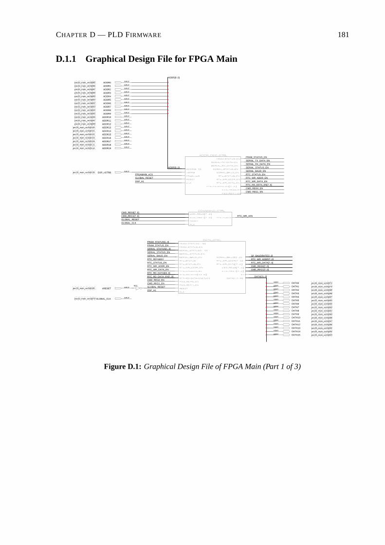
CHAPTER D — PLD FIRMWARE 181
D.1.1 Graphical Design File for FPGA Main
GLOBAL_RESETDSP_H1
RTC_RD_DATA[63..0]
CMD_REG1_ENCMD_REG0_ENRTC_RD_DATA_EN[7..0] DATA[15..0]
RTC_RDYnBSY
RTC_WR_DATA_ENRTC_WR_ADDR_ENRTC_STATUS_EN
RTC_WR_ADDR[7..0]
CMD_REG1[7..0]CMD_REG0[7..0]RTC_WR_DATA[7..0]
FRAM_STATUS_EN
SERIAL_BAUD_ENSERIAL_STATUS_ENSERIAL_STATUS[1..0]
SP_BAUDRATE[2..0]
FRAM_STATUS[1..0]
CMD_REG1[7..0]
GLOBAL_CLKGLOBAL_RESET
CMD_REG0[7..0]RTC_WR_nEN
CMD_REG1_EN
GLOBAL_RESETDSP_H1
CMD_REG0_ENRTC_RD_DATA_EN[7..0]
RTC_WR_ADDR_ENRTC_WR_DATA_EN
FPGAMAIN_nCS
ADDR[9..0]
RTC_STATUS_EN
SERIAL_RX_DATA_ENSERIAL_STATUS_ENSERIAL_BAUD_EN
SERIAL_TX_DATA_ENFRAM_STATUS_EN
ADDR[9..0]
pec33_main_ver3@55DATA13BIDIR
pec33_main_ver3@54DATA14BIDIR
pec33_main_ver3@53DATA15BIDIR
pec33_main_ver3@60DATA9BIDIR
pec33_main_ver3@58DATA10BIDIR
pec33_main_ver3@56DATA12BIDIRpec33_main_ver3@57DATA11BIDIR
pec33_main_ver3@65DATA5BIDIR
pec33_main_ver3@64DATA6BIDIR
pec33_main_ver3@61DATA8BIDIRpec33_main_ver3@63DATA7BIDIR
pec33_main_ver3@180 nRESET INPUT
pec33_main_ver3@79 GLOBAL_CLK INPUT
NOT pec33_main_ver3@70DATA1BIDIR
pec33_main_ver3@69DATA2BIDIR
pec33_main_ver3@67DATA4BIDIRpec33_main_ver3@68DATA3BIDIR
pec33_main_ver3@71DATA0BIDIR
pec33_main_ver3@139 DSP_nSTRB INPUT
pec33_main_ver3@112 ADDR19 INPUT
pec33_main_ver3@102 ADDR15 INPUT
pec33_main_ver3@111 ADDR18 INPUT
pec33_main_ver3@103 ADDR16 INPUT
pec33_main_ver3@104 ADDR17 INPUT
pec33_main_ver3@97 ADDR11 INPUT
pec33_main_ver3@101 ADDR14 INPUT
pec33_main_ver3@99 ADDR12 INPUT
pec33_main_ver3@100 ADDR13 INPUT
pec33_main_ver3@93 ADDR7 INPUT
pec33_main_ver3@96 ADDR10 INPUT
pec33_main_ver3@94 ADDR8 INPUT
pec33_main_ver3@95 ADDR9 INPUT
pec33_main_ver3@88 ADDR3 INPUT
pec33_main_ver3@92 ADDR6 INPUT
pec33_main_ver3@89 ADDR4 INPUT
pec33_main_ver3@90 ADDR5 INPUT
pec33_main_ver3@87 ADDR2 INPUT
pec33_main_ver3@85 ADDR0 INPUT
pec33_main_ver3@86 ADDR1 INPUT
Figure D.1: Graphical Design File of FPGA Main (Part 1 of 3)

CHAPTER D — PLD FIRMWARE 182
GLOBAL_RESETGLOBAL_CLK
FPGANLG_CLKDSP_CLK
GLOBAL_CLK DSP_nRESET
DIP0GLOBAL_RESET
EXBUS1_nINT
EXBUS0_nINT
GLOBAL_RESETDSP_H1
FRAM0_nENFRAM1_nEN
ADDR[23..20]FPGAMAIN_nCS
DSP_nSTRB
SP_BAUDRATE[2..0]GLOBAL_RESETGLOBAL_CLK
DSP_H1SERIAL_STATUS0
SERIAL_STATUS1
GLOBAL_CLKGLOBAL_RESET RTC_RDYnBSY
RTC_WR_nENRTC_WR_DATA[7..0]
RTC_WR_ADDR[7..0] RTC_RD_DATA[63..0]
DSP_H1GLOBAL_RESET FRAM1_nRST
nRESET
FRAM1_nENDSP_RnWDSP_nSTRB
FRAM1_nOEFRAM1_nCE
FRAM1_nWE
GLOBAL_RESETDSP_H1
FRAM0_nRST
DSP_nSTRBDSP_RnWFRAM0_nEN
FRAM0_nCEFRAM0_nOEFRAM0_nWE
FRAM1_RDYnBSYFRAM0_RDYnBSY
pec33_main_ver3@157DSP_CLKOUTPUTpec33_main_ver3@179FPGANLG_CLKOUTPUT
pec33_main_ver3@41EXBUS_GCLKOUTPUT
pec33_main_ver3@159DSP_nRESETOUTPUT
AND2
pec33_main_ver3@166DSP_nINT3OUTPUT
AND2
pec33_main_ver3@164DSP_nINT1OUTPUT
pec33_main_ver3@45EXBUS0_nCSOUTPUT
pec33_main_ver3@75EXBUS1_nCSOUTPUT
pec33_main_ver3@147 ADDR21 INPUT
pec33_main_ver3@148 ADDR22 INPUT
pec33_main_ver3@149 ADDR23 INPUTOR2
pec33_main_ver3@189FPGANLG_nCSOUTPUT
pec33_main_ver3@113 ADDR20 INPUT
pec33_main_ver3@196SP_TXOUTPUT
pec33_main_ver3@173 DSP_FSX0 INPUT
pec33_main_ver3@174 DSP_CLKX0 INPUT
pec33_main_ver3@197 SP_RX INPUT
pec33_main_ver3@176DSP_FSR0OUTPUT
pec33_main_ver3@175DSP_CLKR0OUTPUT
pec33_main_ver3@177DSP_DR0OUTPUTpec33_main_ver3@172 DSP_DX0 INPUT
VCC
pec33_main_ver3@114RTC_SDABIDIRpec33_main_ver3@116RTC_SQW_OUTINPUT
pec33_main_ver3@115RTC_SCLOUTPUT
pec33_main_ver3@121FRAM_STATUS1INPUT
pec33_main_ver3@120FRAM_STATUS0INPUT
pec33_main_ver3@122FRAM1_nCEOUTPUT
AND2
AND3
pec33_main_ver3@128FRAM_nRSTOUTPUT
AND2
pec33_main_ver3@126FRAM_nOEOUTPUT
pec33_main_ver3@127FRAM_nWEOUTPUT
pec33_main_ver3@125FRAM0_nCEOUTPUT
Figure D.2: Graphical Design File of FPGA Main (Part 2 of 3)

CHAPTER D — PLD FIRMWARE 183
SP_RX
DSP_DR0
SP_BAUDRATE2
SERIAL_STATUS0
GLOBAL_RESET SP_BAUDRATE1
SP_BAUDRATE0
GLOBAL_CLK
GLOBAL_RESET
GLOBAL_RESET
GLOBAL_RESET
FRAM_STATUS0
DIP[5..0]
pec33_main_ver3@205 DIP3 INPUT
pec33_main_ver3@207 DIP5 INPUT
pec33_main_ver3@206 DIP4 INPUT
pec33_main_ver3@204 DIP2 INPUT
pec33_main_ver3@203 DIP1 INPUT
pec33_main_ver3@202 DIP0 INPUT
pec33_main_ver3@11 USB_nEOT OUTPUT
pec33_main_ver3@13 USB_XTAL1 OUTPUTpec33_main_ver3@12 USB_nRESET OUTPUT
pec33_main_ver3@14 USB_A0 INPUT
pec33_main_ver3@7 USB_nRD OUTPUT
pec33_main_ver3@10 USB_DMACK OUTPUT
pec33_main_ver3@8 USB_nWR OUTPUT
pec33_main_ver3@9 USB_DMREQ INPUT
pec33_main_ver3@24 USB_SUSPEND BIDIRpec33_main_ver3@19 USB_nCS OUTPUT
pec33_main_ver3@25 USB_nINT INPUT
VCC
pec33_main_ver3@29 USB_DATA4 BIDIR
pec33_main_ver3@26 USB_DATA7 BIDIRpec33_main_ver3@27 USB_DATA6 BIDIRpec33_main_ver3@28 USB_DATA5 BIDIR
pec33_main_ver3@15 USB_DATA0 BIDIR
pec33_main_ver3@18 USB_DATA3 BIDIRpec33_main_ver3@17 USB_DATA2 BIDIRpec33_main_ver3@16 USB_DATA1 BIDIR
pec33_main_ver3@190 OP0_TX OUTPUT
pec33_main_ver3@192 OP1_TX OUTPUTpec33_main_ver3@193 OP1_RX INPUT
VCC
pec33_main_ver3@195 RS232_nEN OUTPUT
pec33_main_ver3@198 RS232_nSHDN OUTPUT
pec33_main_ver3@191 OP0_RX INPUT
VCC
NOT
NOT
pec33_main_ver3@199 CPP_TX OUTPUTpec33_main_ver3@200 CPP_RX INPUT
VCC
VCCpec33_main_ver3@133 LED7 OUTPUTpec33_main_ver3@134 LED6 OUTPUT
NOT
NOT
pec33_main_ver3@187 FPGANLG_nRESET OUTPUT
pec33_main_ver3@158 DSP_nSHZ OUTPUT
NOT
pec33_main_ver3@37 LED3 OUTPUT
pec33_main_ver3@136 LED4 OUTPUT
pec33_main_ver3@135 LED5 OUTPUT
pec33_main_ver3@36 LED2 OUTPUTNOT
NOT
pec33_main_ver3@144 DSP_nHOLDA INPUT
pec33_main_ver3@141 DSP_nIACK INPUT
pec33_main_ver3@183 DSP_H1 INPUT VCC pec33_main_ver3@31 LED1 OUTPUTpec33_main_ver3@30 LED0 OUTPUT
NOT
pec33_main_ver3@143 DSP_nHOLD OUTPUT
pec33_main_ver3@140 DSP_RnW INPUTVCC
pec33_main_ver3@83 EXBUS1_nRESET OUTPUT
pec33_main_ver3@40 EXBUS1_nINTREQ INPUT
pec33_main_ver3@73 EXBUS1_RDYnBSY INPUT
pec33_main_ver3@74 EXBUS1_nINT INPUT
NOT
pec33_main_ver3@167 DSP_XF0 BIDIR
pec33_main_ver3@168 DSP_XF1 BIDIRpec33_main_ver3@47 EXBUS0_RDYnBSY INPUT
pec33_main_ver3@39 EXBUS0_nINTREQ INPUT
pec33_main_ver3@170 DSP_TCLK1 BIDIRpec33_main_ver3@169 DSP_TCLK0 BIDIR
VCC
pec33_main_ver3@44 EXBUS0_nRESET OUTPUT
pec33_main_ver3@46 EXBUS0_nINT INPUT
NOT
pec33_main_ver3@142 DSP_nRDY OUTPUTNOT
Figure D.3: Graphical Design File of FPGA Main (Part 3 of 3)

CHAPTER D — PLD FIRMWARE 184
D.1.2 VHDL Code for the Addr Dec Ctrl Module of FPGA Main-- PEC 33 FPGA Main - Address Decoder Controller 2002-11-07
LIBRARY ieee;
USE ieee.std_logic_1164.all;
USE ieee.std_logic_arith.all;
ENTITY Addr_Dec_Ctrl IS
PORT (
FRAM_STATUS_EN : OUT STD_LOGIC;
SERIAL_TX_DATA_EN : OUT STD_LOGIC;
SERIAL_RX_DATA_EN : OUT STD_LOGIC;
SERIAL_STATUS_EN : OUT STD_LOGIC;
SERIAL_BAUD_EN : OUT STD_LOGIC;
RTC_STATUS_EN : OUT STD_LOGIC;
RTC_WR_ADDR_EN : OUT STD_LOGIC;
RTC_WR_DATA_EN : OUT STD_LOGIC;
RTC_RD_DATA_EN : OUT STD_LOGIC_VECTOR ( 7 DOWNTO 0 );
CMD_REG0_EN : OUT STD_LOGIC;
CMD_REG1_EN : OUT STD_LOGIC;
ADDR : IN STD_LOGIC_VECTOR ( 9 DOWNTO 0 );
nSTRB : IN STD_LOGIC;
FPGA_nCS : IN STD_LOGIC;
RESET : IN STD_LOGIC;
CLK : IN STD_LOGIC
);
END Addr_Dec_Ctrl;
ARCHITECTURE a OF Addr_Dec_Ctrl IS
TYPE statetype IS ( state0, state1, state2, state3 );
CONSTANT serial_tx_data_addr : INTEGER := 0;
CONSTANT serial_rx_data_addr : INTEGER := 1;
CONSTANT serial_status_addr : INTEGER := 2;
CONSTANT serial_baud_addr : INTEGER := 3;
CONSTANT fram_status_addr : INTEGER := 8;
CONSTANT rtc_status_addr : INTEGER := 16;
CONSTANT rtc_wr_addr_addr : INTEGER := 17;
CONSTANT rtc_wr_data_addr : INTEGER := 18;
CONSTANT rtc_rd_data_addr : INTEGER := 19;
CONSTANT cmd_reg0_addr : INTEGER := 102;
CONSTANT cmd_reg1_addr : INTEGER := 103;
SIGNAL trig_SERIAL_TX_DATA_EN : STD_LOGIC;
SIGNAL trig_SERIAL_RX_DATA_EN : STD_LOGIC;
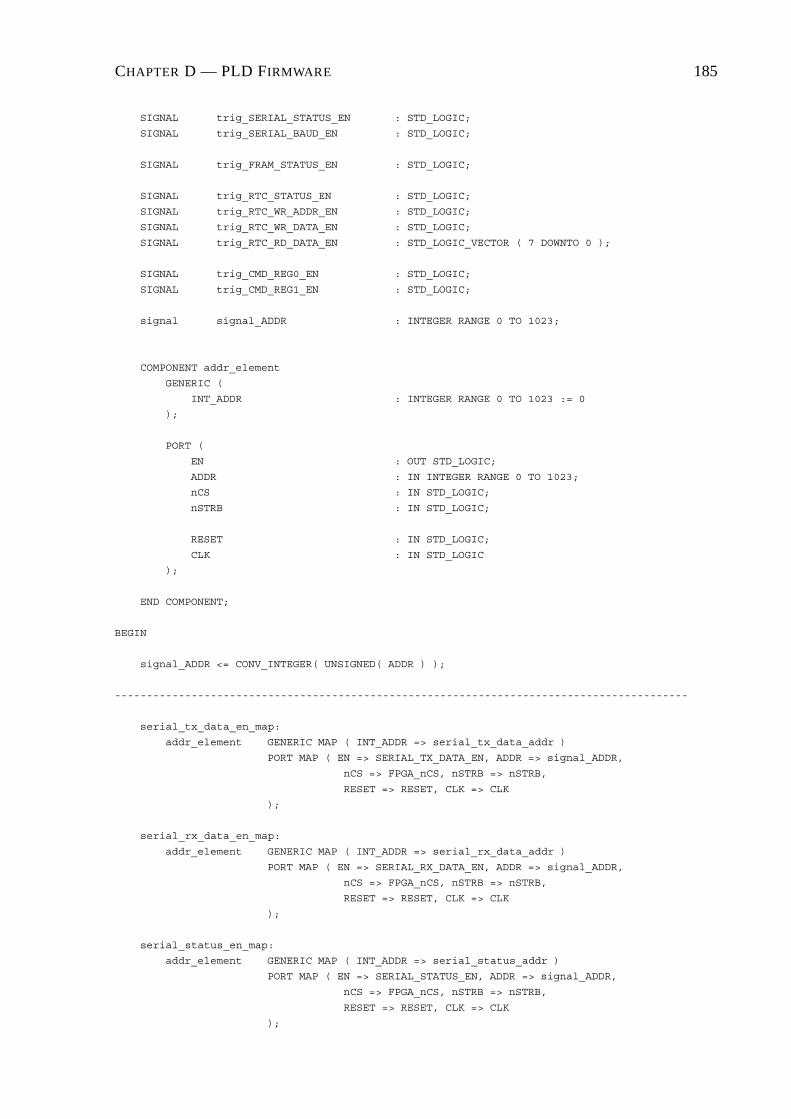
CHAPTER D — PLD FIRMWARE 185
SIGNAL trig_SERIAL_STATUS_EN : STD_LOGIC;
SIGNAL trig_SERIAL_BAUD_EN : STD_LOGIC;
SIGNAL trig_FRAM_STATUS_EN : STD_LOGIC;
SIGNAL trig_RTC_STATUS_EN : STD_LOGIC;
SIGNAL trig_RTC_WR_ADDR_EN : STD_LOGIC;
SIGNAL trig_RTC_WR_DATA_EN : STD_LOGIC;
SIGNAL trig_RTC_RD_DATA_EN : STD_LOGIC_VECTOR ( 7 DOWNTO 0 );
SIGNAL trig_CMD_REG0_EN : STD_LOGIC;
SIGNAL trig_CMD_REG1_EN : STD_LOGIC;
signal signal_ADDR : INTEGER RANGE 0 TO 1023;
COMPONENT addr_element
GENERIC (
INT_ADDR : INTEGER RANGE 0 TO 1023 := 0
);
PORT (
EN : OUT STD_LOGIC;
ADDR : IN INTEGER RANGE 0 TO 1023;
nCS : IN STD_LOGIC;
nSTRB : IN STD_LOGIC;
RESET : IN STD_LOGIC;
CLK : IN STD_LOGIC
);
END COMPONENT;
BEGIN
signal_ADDR <= CONV_INTEGER( UNSIGNED( ADDR ) );
------------------------------------------------------------------------------------------
serial_tx_data_en_map:
addr_element GENERIC MAP ( INT_ADDR => serial_tx_data_addr )
PORT MAP ( EN => SERIAL_TX_DATA_EN, ADDR => signal_ADDR,
nCS => FPGA_nCS, nSTRB => nSTRB,
RESET => RESET, CLK => CLK
);
serial_rx_data_en_map:
addr_element GENERIC MAP ( INT_ADDR => serial_rx_data_addr )
PORT MAP ( EN => SERIAL_RX_DATA_EN, ADDR => signal_ADDR,
nCS => FPGA_nCS, nSTRB => nSTRB,
RESET => RESET, CLK => CLK
);
serial_status_en_map:
addr_element GENERIC MAP ( INT_ADDR => serial_status_addr )
PORT MAP ( EN => SERIAL_STATUS_EN, ADDR => signal_ADDR,
nCS => FPGA_nCS, nSTRB => nSTRB,
RESET => RESET, CLK => CLK
);

CHAPTER D — PLD FIRMWARE 186
serial_baud_en_map:
addr_element GENERIC MAP ( INT_ADDR => serial_baud_addr )
PORT MAP ( EN => SERIAL_BAUD_EN, ADDR => signal_ADDR,
nCS => FPGA_nCS, nSTRB => nSTRB,
RESET => RESET, CLK => CLK
);
------------------------------------------------------------------------------------------
fram_status_en_map:
addr_element GENERIC MAP ( INT_ADDR => fram_status_addr )
PORT MAP ( EN => FRAM_STATUS_EN, ADDR => signal_ADDR,
nCS => FPGA_nCS, nSTRB => nSTRB,
RESET => RESET, CLK => CLK
);
------------------------------------------------------------------------------------------
rtc_status_en_map:
addr_element GENERIC MAP ( INT_ADDR => rtc_status_addr )
PORT MAP ( EN => RTC_STATUS_EN, ADDR => signal_ADDR,
nCS => FPGA_nCS, nSTRB => nSTRB,
RESET => RESET, CLK => CLK
);
rtc_wr_addr_en_map:
addr_element GENERIC MAP ( INT_ADDR => rtc_wr_addr_addr )
PORT MAP ( EN => RTC_WR_ADDR_EN, ADDR => signal_ADDR,
nCS => FPGA_nCS, nSTRB => nSTRB,
RESET => RESET, CLK => CLK
);
rtc_wr_data_en_map:
addr_element GENERIC MAP ( INT_ADDR => rtc_wr_data_addr )
PORT MAP ( EN => RTC_WR_DATA_EN, ADDR => signal_ADDR,
nCS => FPGA_nCS, nSTRB => nSTRB,
RESET => RESET, CLK => CLK
);
rtc_rd_data0_en_map:
addr_element GENERIC MAP ( INT_ADDR => rtc_rd_data_addr )
PORT MAP ( EN => RTC_RD_DATA_EN( 0 ), ADDR => signal_ADDR,
nCS => FPGA_nCS, nSTRB => nSTRB,
RESET => RESET, CLK => CLK
);
rtc_rd_data1_en_map:
addr_element GENERIC MAP ( INT_ADDR => ( rtc_rd_data_addr + 1) )
PORT MAP ( EN => RTC_RD_DATA_EN( 1 ), ADDR => signal_ADDR,
nCS => FPGA_nCS, nSTRB => nSTRB,
RESET => RESET, CLK => CLK
);
rtc_rd_data2_en_map:
addr_element GENERIC MAP ( INT_ADDR => ( rtc_rd_data_addr + 2) )
PORT MAP ( EN => RTC_RD_DATA_EN( 2 ), ADDR => signal_ADDR,
nCS => FPGA_nCS, nSTRB => nSTRB,
RESET => RESET, CLK => CLK
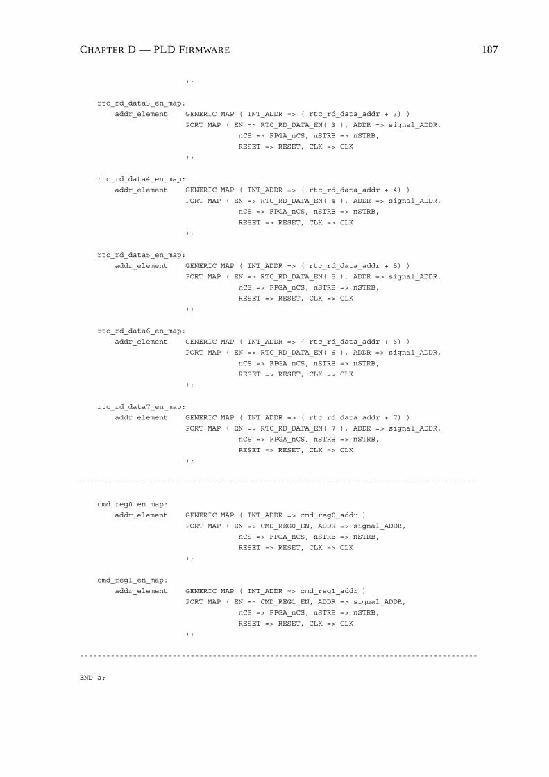
CHAPTER D — PLD FIRMWARE 187
);
rtc_rd_data3_en_map:
addr_element GENERIC MAP ( INT_ADDR => ( rtc_rd_data_addr + 3) )
PORT MAP ( EN => RTC_RD_DATA_EN( 3 ), ADDR => signal_ADDR,
nCS => FPGA_nCS, nSTRB => nSTRB,
RESET => RESET, CLK => CLK
);
rtc_rd_data4_en_map:
addr_element GENERIC MAP ( INT_ADDR => ( rtc_rd_data_addr + 4) )
PORT MAP ( EN => RTC_RD_DATA_EN( 4 ), ADDR => signal_ADDR,
nCS => FPGA_nCS, nSTRB => nSTRB,
RESET => RESET, CLK => CLK
);
rtc_rd_data5_en_map:
addr_element GENERIC MAP ( INT_ADDR => ( rtc_rd_data_addr + 5) )
PORT MAP ( EN => RTC_RD_DATA_EN( 5 ), ADDR => signal_ADDR,
nCS => FPGA_nCS, nSTRB => nSTRB,
RESET => RESET, CLK => CLK
);
rtc_rd_data6_en_map:
addr_element GENERIC MAP ( INT_ADDR => ( rtc_rd_data_addr + 6) )
PORT MAP ( EN => RTC_RD_DATA_EN( 6 ), ADDR => signal_ADDR,
nCS => FPGA_nCS, nSTRB => nSTRB,
RESET => RESET, CLK => CLK
);
rtc_rd_data7_en_map:
addr_element GENERIC MAP ( INT_ADDR => ( rtc_rd_data_addr + 7) )
PORT MAP ( EN => RTC_RD_DATA_EN( 7 ), ADDR => signal_ADDR,
nCS => FPGA_nCS, nSTRB => nSTRB,
RESET => RESET, CLK => CLK
);
------------------------------------------------------------------------------------------
cmd_reg0_en_map:
addr_element GENERIC MAP ( INT_ADDR => cmd_reg0_addr )
PORT MAP ( EN => CMD_REG0_EN, ADDR => signal_ADDR,
nCS => FPGA_nCS, nSTRB => nSTRB,
RESET => RESET, CLK => CLK
);
cmd_reg1_en_map:
addr_element GENERIC MAP ( INT_ADDR => cmd_reg1_addr )
PORT MAP ( EN => CMD_REG1_EN, ADDR => signal_ADDR,
nCS => FPGA_nCS, nSTRB => nSTRB,
RESET => RESET, CLK => CLK
);
------------------------------------------------------------------------------------------
END a;

CHAPTER D — PLD FIRMWARE 188
D.1.3 VHDL Code for the Addr Element Module of FPGA Main-- FPGA Main - ADDR_Element 2002-11-07
LIBRARY ieee;
USE ieee.std_logic_1164.all;
USE ieee.std_logic_arith.all;
ENTITY addr_element IS
GENERIC (
INT_ADDR : INTEGER RANGE 0 TO 1023 := 0
);
PORT (
EN : OUT STD_LOGIC;
ADDR : IN INTEGER RANGE 0 TO 1023;
nCS : IN STD_LOGIC;
nSTRB : IN STD_LOGIC;
RESET : IN STD_LOGIC;
CLK : IN STD_LOGIC
);
END addr_element;
ARCHITECTURE a OF addr_element IS
BEGIN
reg_en_proc:
PROCESS ( CLK, RESET )
BEGIN
IF ( RESET = ’1’ ) THEN
EN <= ’0’;
ELSIF ( CLK’event )and( CLK = ’1’ ) THEN
IF ( nSTRB = ’0’ )and( INT_ADDR = ADDR ) THEN
EN <= not nCS;
ELSE
EN <= ’0’;
END IF;
END IF;
END PROCESS reg_en_proc;
END a;

CHAPTER D — PLD FIRMWARE 189
D.1.4 VHDL Code for the Command Ctrl Module of FPGA Main-- FPGA Main - Command Controller 2002-11-07
LIBRARY ieee;
USE ieee.std_logic_1164.all;
USE ieee.std_logic_arith.all;
ENTITY Command_Ctrl IS
PORT (
RTC_nLOAD : OUT STD_LOGIC;
CMD_REG0 : IN STD_LOGIC_VECTOR ( 7 DOWNTO 0 );
CMD_REG1 : IN STD_LOGIC_VECTOR ( 7 DOWNTO 0 );
RESET : IN STD_LOGIC;
CLK : IN STD_LOGIC
);
END Command_Ctrl;
ARCHITECTURE a OF Command_Ctrl IS
TYPE statetype IS ( state0, state1, state2, state3 );
-- Current and next state of the type 0 command state machine
SIGNAL sm0_state : statetype;
SIGNAL nextsm0_state : statetype;
-- Start signal for the type 0 command state machine
SIGNAL start_sm0 : STD_LOGIC;
-- New and previous command output register for type 0 commands
SIGNAL signal_cmd_reg0 : STD_LOGIC_VECTOR ( 7 DOWNTO 0 );
SIGNAL signal_prevcmd_reg0 : STD_LOGIC_VECTOR ( 7 DOWNTO 0 );
-- New command output register for type 0 commands
SIGNAL signal_cmd_reg1 : STD_LOGIC_VECTOR ( 7 DOWNTO 0 );
BEGIN
RTC_nLOAD <= signal_cmd_reg0(0);
------------------------------------------------------------------------------------------
reg0_proc:
PROCESS ( CLK, RESET )
BEGIN
IF ( RESET = ’1’ ) THEN
signal_cmd_reg0 <= "11111111";
ELSIF ( CLK’event )and( CLK = ’1’ ) THEN
IF ( sm0_state = state0 ) THEN
signal_cmd_reg0 <= "11111111";

CHAPTER D — PLD FIRMWARE 190
ELSIF ( sm0_state = state1 ) THEN
signal_cmd_reg0 <= not( CMD_REG0 );
END IF;
END IF;
END PROCESS reg0_proc;
------------------------------------------------------------------------------------------
reg1_proc:
PROCESS ( CLK, RESET )
BEGIN
IF ( RESET = ’1’ ) THEN
signal_cmd_reg1 <= "11111111";
ELSIF ( CLK’event )and( CLK = ’1’ ) THEN
signal_cmd_reg1 <= not( CMD_REG1 );
END IF;
END PROCESS reg1_proc;
------------------------------------------------------------------------------------------
sm0_proc:
PROCESS ( sm0_state )
BEGIN
CASE sm0_state IS
WHEN state0 =>
nextsm0_state <= state1;
WHEN state1 =>
nextsm0_state <= state2;
WHEN state2 =>
nextsm0_state <= state3;
WHEN state3 =>
nextsm0_state <= state0;
END CASE;
END PROCESS sm0_proc;
------------------------------------------------------------------------------------------
sm0_ctrl_proc:
PROCESS ( CLK, RESET )
BEGIN
IF ( RESET = ’1’ ) THEN
sm0_state <= state0;
ELSIF ( CLK’event )and( CLK = ’1’ ) THEN
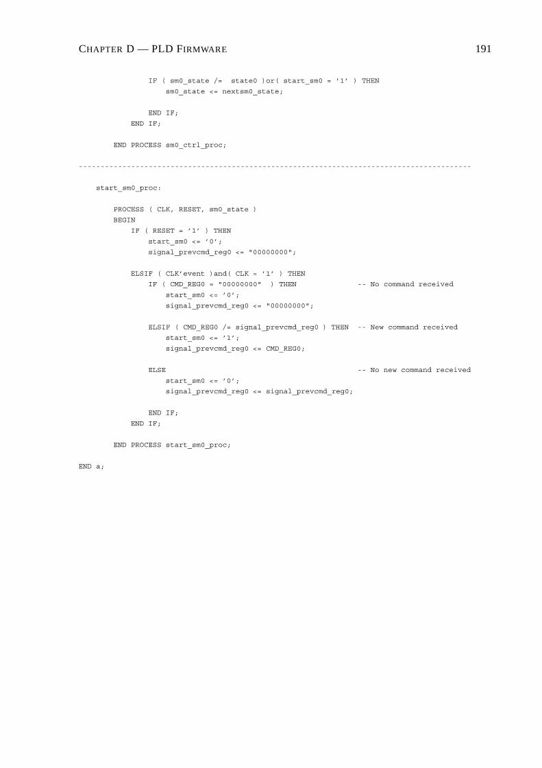
CHAPTER D — PLD FIRMWARE 191
IF ( sm0_state /= state0 )or( start_sm0 = ’1’ ) THEN
sm0_state <= nextsm0_state;
END IF;
END IF;
END PROCESS sm0_ctrl_proc;
------------------------------------------------------------------------------------------
start_sm0_proc:
PROCESS ( CLK, RESET, sm0_state )
BEGIN
IF ( RESET = ’1’ ) THEN
start_sm0 <= ’0’;
signal_prevcmd_reg0 <= "00000000";
ELSIF ( CLK’event )and( CLK = ’1’ ) THEN
IF ( CMD_REG0 = "00000000" ) THEN -- No command received
start_sm0 <= ’0’;
signal_prevcmd_reg0 <= "00000000";
ELSIF ( CMD_REG0 /= signal_prevcmd_reg0 ) THEN -- New command received
start_sm0 <= ’1’;
signal_prevcmd_reg0 <= CMD_REG0;
ELSE -- No new command received
start_sm0 <= ’0’;
signal_prevcmd_reg0 <= signal_prevcmd_reg0;
END IF;
END IF;
END PROCESS start_sm0_proc;
END a;

CHAPTER D — PLD FIRMWARE 192
D.1.5 VHDL Code for the Data Ctrl Module of FPGA Main-- PEC 33 FPGA Main - Data Controller 2002-11-07
LIBRARY ieee;
USE ieee.std_logic_1164.all;
USE ieee.std_logic_arith.all;
ENTITY Data_Ctrl IS
PORT (
FRAM_STATUS : IN STD_LOGIC_VECTOR ( 1 DOWNTO 0 );
FRAM_STATUS_EN : IN STD_LOGIC;
SERIAL_STATUS : IN STD_LOGIC_VECTOR ( 1 DOWNTO 0 );
SERIAL_STATUS_EN : IN STD_LOGIC;
SERIAL_BAUD : OUT STD_LOGIC_VECTOR ( 2 DOWNTO 0 );
SERIAL_BAUD_EN : IN STD_LOGIC;
RTC_STATUS : IN STD_LOGIC;
RTC_STATUS_EN : IN STD_LOGIC;
RTC_WR_ADDR : OUT STD_LOGIC_VECTOR ( 7 DOWNTO 0 );
RTC_WR_ADDR_EN : IN STD_LOGIC;
RTC_WR_DATA : OUT STD_LOGIC_VECTOR ( 7 DOWNTO 0 );
RTC_WR_DATA_EN : IN STD_LOGIC;
RTC_RD_DATA : IN STD_LOGIC_VECTOR ( 63 DOWNTO 0 );
RTC_RD_DATA_EN : IN STD_LOGIC_VECTOR ( 7 DOWNTO 0 );
CMD_REG0 : OUT STD_LOGIC_VECTOR ( 7 DOWNTO 0 );
CMD_REG0_EN : IN STD_LOGIC;
CMD_REG1 : OUT STD_LOGIC_VECTOR ( 7 DOWNTO 0 );
CMD_REG1_EN : IN STD_LOGIC;
RnW : OUT STD_LOGIC;
DATA : INOUT STD_LOGIC_VECTOR ( 15 DOWNTO 0 );
RESET : IN STD_LOGIC;
CLK : IN STD_LOGIC
);
END Data_Ctrl;
ARCHITECTURE a OF Data_Ctrl IS
SIGNAL signal_SERIAL_TX_DATA : STD_LOGIC_VECTOR ( 7 DOWNTO 0 );
SIGNAL signal_SERIAL_RX_DATA : STD_LOGIC_VECTOR ( 7 DOWNTO 0 );
SIGNAL signal_SERIAL_STATUS : STD_LOGIC_VECTOR ( 1 DOWNTO 0 );
SIGNAL signal_SERIAL_BAUD : STD_LOGIC_VECTOR ( 2 DOWNTO 0 );
SIGNAL signal_FRAM_STATUS : STD_LOGIC_VECTOR ( 1 DOWNTO 0 );
SIGNAL signal_RTC_STATUS : STD_LOGIC;
SIGNAL signal_RTC_WR_ADDR : STD_LOGIC_VECTOR ( 7 DOWNTO 0 );

CHAPTER D — PLD FIRMWARE 193
SIGNAL signal_RTC_WR_DATA : STD_LOGIC_VECTOR ( 7 DOWNTO 0 );
SIGNAL signal_RTC_RD_DATA : STD_LOGIC_VECTOR ( 63 DOWNTO 0 );
SIGNAL signal_CMD_REG0 : STD_LOGIC_VECTOR ( 7 DOWNTO 0 );
SIGNAL signal_CMD_REG1 : STD_LOGIC_VECTOR ( 7 DOWNTO 0 );
SIGNAL signal_DATA_OUT : STD_LOGIC_VECTOR ( 15 DOWNTO 0 );
SIGNAL signal_DATA_IN : STD_LOGIC_VECTOR ( 15 DOWNTO 0 );
SIGNAL signal_RnW : STD_LOGIC;
COMPONENT Bidir
GENERIC (
n : INTEGER RANGE 0 TO 31 := 15
);
PORT (
BIDIR : INOUT STD_LOGIC_VECTOR ( n DOWNTO 0 );
RnW : IN STD_LOGIC;
CLK : IN STD_LOGIC;
IN_DATA : IN STD_LOGIC_VECTOR ( n DOWNTO 0 );
OUT_DATA : OUT STD_LOGIC_VECTOR ( n DOWNTO 0 )
);
END COMPONENT;
COMPONENT mybuf
GENERIC (
n : INTEGER RANGE 0 TO 15 := 15
);
PORT (
RESET : IN STD_LOGIC;
SEL : IN STD_LOGIC;
IN_DATA : IN STD_LOGIC_VECTOR ( n DOWNTO 0 );
OUT_DATA : OUT STD_LOGIC_VECTOR ( n DOWNTO 0 )
);
END COMPONENT mybuf;
BEGIN
signal_FRAM_STATUS <= FRAM_STATUS;
SERIAL_BAUD <= signal_SERIAL_BAUD;
signal_SERIAL_STATUS <= SERIAL_STATUS;
signal_RTC_STATUS <= RTC_STATUS;
signal_RTC_RD_DATA <= RTC_RD_DATA;
RTC_WR_ADDR <= signal_RTC_WR_ADDR;
RTC_WR_DATA <= signal_RTC_WR_DATA;
CMD_REG0 <= signal_CMD_REG0;
CMD_REG1 <= signal_CMD_REG1;

CHAPTER D — PLD FIRMWARE 194
------------------------------------------------------------------------------------------
serial_baud_map:
MyBuf GENERIC MAP ( n => 2 )
PORT MAP ( RESET => RESET, SEL => SERIAL_BAUD_EN,
IN_DATA => signal_DATA_IN ( 2 DOWNTO 0 ),
OUT_DATA => signal_SERIAL_BAUD );
------------------------------------------------------------------------------------------
rtc_wr_addr_map:
MyBuf GENERIC MAP ( n => 7 )
PORT MAP ( RESET => RESET, SEL => RTC_WR_ADDR_EN,
IN_DATA => signal_DATA_IN ( 7 DOWNTO 0 ),
OUT_DATA => signal_RTC_WR_ADDR );
rtc_wr_data_map:
MyBuf GENERIC MAP ( n => 7 )
PORT MAP ( RESET => RESET, SEL => RTC_WR_DATA_EN,
IN_DATA => signal_DATA_IN ( 7 DOWNTO 0 ),
OUT_DATA => signal_RTC_WR_DATA );
------------------------------------------------------------------------------------------
cmd_reg0_map:
MyBuf GENERIC MAP ( n => 7 )
PORT MAP ( RESET => RESET, SEL => CMD_REG0_EN,
IN_DATA => signal_DATA_IN ( 7 DOWNTO 0 ),
OUT_DATA => signal_CMD_REG0 );
cmd_reg1_map:
MyBuf GENERIC MAP ( n => 7 )
PORT MAP ( RESET => RESET, SEL => CMD_REG1_EN,
IN_DATA => signal_DATA_IN ( 7 DOWNTO 0 ),
OUT_DATA => signal_CMD_REG1 );
------------------------------------------------------------------------------------------
bidir_bus_map:
bidir GENERIC MAP ( n => 15 )
PORT MAP ( BIDIR => DATA, RnW => signal_RnW, CLK => CLK,
IN_DATA => signal_DATA_OUT,
OUT_DATA => signal_DATA_IN );
------------------------------------------------------------------------------------------
signal_RnW <= ’0’ WHEN ( SERIAL_STATUS_EN = ’1’ )or
( FRAM_STATUS_EN = ’1’ )or
( RTC_STATUS_EN = ’1’ )or
( RTC_RD_DATA_EN /= "00000000" ) ELSE
’1’;
RnW <= signal_RnW;
signal_DATA_OUT( 0 )
<= signal_SERIAL_STATUS ( 0 ) WHEN ( SERIAL_STATUS_EN = ’1’ ) ELSE
signal_FRAM_STATUS ( 0 ) WHEN ( FRAM_STATUS_EN = ’1’ ) ELSE
signal_RTC_STATUS WHEN ( RTC_STATUS_EN = ’1’ ) ELSE

CHAPTER D — PLD FIRMWARE 195
signal_RTC_RD_DATA ( 0 ) WHEN ( RTC_RD_DATA_EN = "00000001" ) ELSE
signal_RTC_RD_DATA ( 8 ) WHEN ( RTC_RD_DATA_EN = "00000010" ) ELSE
signal_RTC_RD_DATA ( 16 ) WHEN ( RTC_RD_DATA_EN = "00000100" ) ELSE
signal_RTC_RD_DATA ( 24 ) WHEN ( RTC_RD_DATA_EN = "00001000" ) ELSE
signal_RTC_RD_DATA ( 32 ) WHEN ( RTC_RD_DATA_EN = "00010000" ) ELSE
signal_RTC_RD_DATA ( 40 ) WHEN ( RTC_RD_DATA_EN = "00100000" ) ELSE
signal_RTC_RD_DATA ( 48 ) WHEN ( RTC_RD_DATA_EN = "01000000" ) ELSE
signal_RTC_RD_DATA ( 56 ) WHEN ( RTC_RD_DATA_EN = "10000000" ) ELSE
’1’;
signal_DATA_OUT( 1 )
<= signal_SERIAL_STATUS ( 1 ) WHEN ( SERIAL_STATUS_EN = ’1’ ) ELSE
signal_FRAM_STATUS ( 1 ) WHEN ( FRAM_STATUS_EN = ’1’ ) ELSE
signal_RTC_RD_DATA ( 1 ) WHEN ( RTC_RD_DATA_EN = "00000001" ) ELSE
signal_RTC_RD_DATA ( 9 ) WHEN ( RTC_RD_DATA_EN = "00000010" ) ELSE
signal_RTC_RD_DATA ( 17 ) WHEN ( RTC_RD_DATA_EN = "00000100" ) ELSE
signal_RTC_RD_DATA ( 25 ) WHEN ( RTC_RD_DATA_EN = "00001000" ) ELSE
signal_RTC_RD_DATA ( 33 ) WHEN ( RTC_RD_DATA_EN = "00010000" ) ELSE
signal_RTC_RD_DATA ( 41 ) WHEN ( RTC_RD_DATA_EN = "00100000" ) ELSE
signal_RTC_RD_DATA ( 49 ) WHEN ( RTC_RD_DATA_EN = "01000000" ) ELSE
signal_RTC_RD_DATA ( 57 ) WHEN ( RTC_RD_DATA_EN = "10000000" ) ELSE
’1’;
signal_DATA_OUT( 7 DOWNTO 2 )
<= signal_RTC_RD_DATA ( 7 DOWNTO 2 ) WHEN ( RTC_RD_DATA_EN = "00000001" ) ELSE
signal_RTC_RD_DATA ( 15 DOWNTO 10 ) WHEN ( RTC_RD_DATA_EN = "00000010" ) ELSE
signal_RTC_RD_DATA ( 23 DOWNTO 18 ) WHEN ( RTC_RD_DATA_EN = "00000100" ) ELSE
signal_RTC_RD_DATA ( 31 DOWNTO 26 ) WHEN ( RTC_RD_DATA_EN = "00001000" ) ELSE
signal_RTC_RD_DATA ( 39 DOWNTO 34 ) WHEN ( RTC_RD_DATA_EN = "00010000" ) ELSE
signal_RTC_RD_DATA ( 47 DOWNTO 42 ) WHEN ( RTC_RD_DATA_EN = "00100000" ) ELSE
signal_RTC_RD_DATA ( 55 DOWNTO 50 ) WHEN ( RTC_RD_DATA_EN = "01000000" ) ELSE
signal_RTC_RD_DATA ( 63 DOWNTO 58 ) WHEN ( RTC_RD_DATA_EN = "10000000" ) ELSE
"00000000000000";
signal_DATA_OUT( 15 DOWNTO 8 ) <= "00000000";
END a;
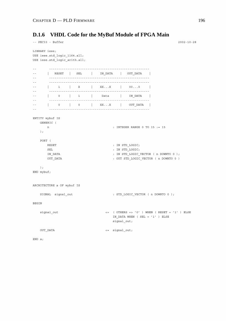
CHAPTER D — PLD FIRMWARE 196
D.1.6 VHDL Code for the MyBuf Module of FPGA Main-- PEC33 - Buffer 2002-10-28
LIBRARY ieee;
USE ieee.std_logic_1164.all;
USE ieee.std_logic_arith.all;
-- -------------------------------------------------------
-- | RESET | SEL | IN_DATA | OUT_DATA |
-- -------------------------------------------------------
-- -------------------------------------------------------
-- | 1 | X | XX...X | 00...0 |
-- -------------------------------------------------------
-- | 0 | 1 | Data | IN_DATA |
-- -------------------------------------------------------
-- | 0 | 0 | XX...X | OUT_DATA |
-- -------------------------------------------------------
ENTITY mybuf IS
GENERIC (
n : INTEGER RANGE 0 TO 15 := 15
);
PORT (
RESET : IN STD_LOGIC;
SEL : IN STD_LOGIC;
IN_DATA : IN STD_LOGIC_VECTOR ( n DOWNTO 0 );
OUT_DATA : OUT STD_LOGIC_VECTOR ( n DOWNTO 0 )
);
END mybuf;
ARCHITECTURE a OF mybuf IS
SIGNAL signal_out : STD_LOGIC_VECTOR ( n DOWNTO 0 );
BEGIN
signal_out <= ( OTHERS => ’0’ ) WHEN ( RESET = ’1’ ) ELSE
IN_DATA WHEN ( SEL = ’1’ ) ELSE
signal_out;
OUT_DATA <= signal_out;
END a;

CHAPTER D — PLD FIRMWARE 197
D.1.7 VHDL Code for the BiDir Module of FPGA Main-- Bidirectional Bus 2002-11-07
LIBRARY ieee;
USE ieee.std_logic_1164.all;
USE ieee.std_logic_arith.all;
-- -------------------------------------------------------------------
-- | RnW | BIDIR | IN_DATA | OUT_DATA |
-- -------------------------------------------------------------------
-- -------------------------------------------------------------------
-- | 1 | ZZZZZZZZZZZZZZZZ | XXXXXXXXXXXXXXXX | BIDIR |
-- -------------------------------------------------------------------
-- | 0 | IN_DATA | Data | BIDIR |
-- -------------------------------------------------------------------
ENTITY Bidir IS
GENERIC (
n : INTEGER RANGE 0 TO 31 := 15
);
PORT (
BIDIR : INOUT STD_LOGIC_VECTOR ( n DOWNTO 0 );
RnW : IN STD_LOGIC;
CLK : IN STD_LOGIC;
IN_DATA : IN STD_LOGIC_VECTOR ( n DOWNTO 0 );
OUT_DATA : OUT STD_LOGIC_VECTOR ( n DOWNTO 0 )
);
END Bidir;
ARCHITECTURE maxpld OF Bidir IS
SIGNAL a : STD_LOGIC_VECTOR ( n DOWNTO 0 );
SIGNAL b : STD_LOGIC_VECTOR ( n DOWNTO 0 );
BEGIN
PROCESS ( CLK )
BEGIN
IF ( CLK’event )and( CLK = ’0’ ) THEN
a <= IN_DATA;
OUT_DATA <= b;
END IF;
END PROCESS;
PROCESS ( RnW, BIDIR )
BEGIN
IF ( RnW = ’1’ ) THEN
BIDIR <= ( others => ’Z’ );
b <= BIDIR;
ELSE
BIDIR <= a;

CHAPTER D — PLD FIRMWARE 198
b <= BIDIR;
END IF;
END PROCESS;
END maxpld;

CHAPTER D — PLD FIRMWARE 199
D.1.8 VHDL Code for the FRAM Ctrl Module of FPGA Main-- PEC33 Main - Flash RAM Controller 2002-11-07
LIBRARY ieee;
USE ieee.std_logic_1164.all;
USE ieee.std_logic_arith.all;
ENTITY FRAM_Ctrl IS
PORT (
FRAM_nCE : OUT STD_LOGIC;
FRAM_nOE : OUT STD_LOGIC;
FRAM_nWE : OUT STD_LOGIC;
FRAM_nRST : OUT STD_LOGIC;
DSP_nSTRB : IN STD_LOGIC;
DSP_RnW : IN STD_LOGIC;
nEN : IN STD_LOGIC;
RESET : IN STD_LOGIC;
CLK : IN STD_LOGIC --75MHZ DSP_H1
);
END FRAM_Ctrl;
ARCHITECTURE a OF FRAM_Ctrl IS
TYPE fram_statetype IS ( idle_state, wr_state_start, wr_state_end, rd_state );
SIGNAL state, next_state : fram_statetype;
SIGNAL state_cntr : INTEGER RANGE 0 TO 15;
SIGNAL signal_FRAM_nCE : STD_LOGIC;
SIGNAL signal_FRAM_nOE : STD_LOGIC;
SIGNAL signal_FRAM_nWE : STD_LOGIC;
BEGIN
FRAM_nRST <= ’1’;
FRAM_nCE <= signal_FRAM_nCE WHEN DSP_nSTRB = ’0’ ELSE ’1’;
FRAM_nOE <= signal_FRAM_nOE WHEN DSP_nSTRB = ’0’ ELSE ’1’;
FRAM_nWE <= signal_FRAM_nWE WHEN DSP_nSTRB = ’0’ ELSE ’1’;
------------------------------------------------------------------------------------------
fram_ctrl_proc:
PROCESS ( state )
BEGIN
IF ( state = idle_state ) THEN
signal_FRAM_nCE <= ’1’;
signal_FRAM_nOE <= ’1’;
signal_FRAM_nWE <= ’1’;
ELSIF ( state = wr_state_start ) THEN
signal_FRAM_nCE <= ’0’;
signal_FRAM_nOE <= ’1’;
signal_FRAM_nWE <= ’0’;
ELSIF ( state = wr_state_end ) THEN

CHAPTER D — PLD FIRMWARE 200
signal_FRAM_nCE <= ’0’;
signal_FRAM_nOE <= ’1’;
signal_FRAM_nWE <= ’1’;
ELSIF ( state = rd_state ) THEN
signal_FRAM_nCE <= ’0’;
signal_FRAM_nOE <= ’0’;
signal_FRAM_nWE <= ’1’;
END IF;
END PROCESS fram_ctrl_proc;
------------------------------------------------------------------------------------------
sm_proc:
PROCESS ( state )
BEGIN
CASE state IS
WHEN idle_state =>
next_state <= idle_state;
WHEN wr_state_start =>
next_state <= wr_state_end;
WHEN wr_state_end =>
next_state <= idle_state;
WHEN rd_state =>
next_state <= idle_state;
END CASE;
END PROCESS sm_proc;
------------------------------------------------------------------------------------------
sm_ctrl_proc:
PROCESS ( CLK, RESET )
BEGIN
IF ( RESET = ’1’ ) THEN
state <= idle_state;
ELSIF ( CLK’event )and( CLK = ’0’ ) THEN
IF ( nEN = ’0’ )and( DSP_nSTRB = ’0’ ) THEN
IF ( state = idle_state ) THEN
IF ( DSP_RnW = ’1’ ) THEN
state <= rd_state;
ELSE
state <= wr_state_start;

CHAPTER D — PLD FIRMWARE 201
END IF;
ELSIF ( state = wr_state_start ) THEN
IF ( state_cntr <= 2 ) THEN
state <= wr_state_start;
ELSE
state <= next_state;
END IF;
ELSIF ( state = wr_state_end ) THEN
IF ( state_cntr <= 5 ) THEN
state <= wr_state_end;
ELSE
state <= next_state;
END IF;
ELSIF ( state = rd_state ) THEN
IF ( state_cntr < 6 ) THEN
state <= rd_state;
ELSE
state <= next_state;
END IF;
END IF;
ELSE
state <= idle_state;
END IF;
END IF;
END PROCESS sm_ctrl_proc;
------------------------------------------------------------------------------------------
state_cntr_proc:
PROCESS ( CLK, RESET )
BEGIN
IF ( RESET = ’1’ ) THEN
state_cntr <= 0;
ELSIF ( CLK’event )and( CLK = ’1’ ) THEN
IF ( nEN = ’0’ )and( state /= idle_state ) THEN
state_cntr <= state_cntr+1;
ELSE
state_cntr <= 0;
CHAPTER D — PLD FIRMWARE 202
END IF;
END IF;
END PROCESS state_cntr_proc;
END a;
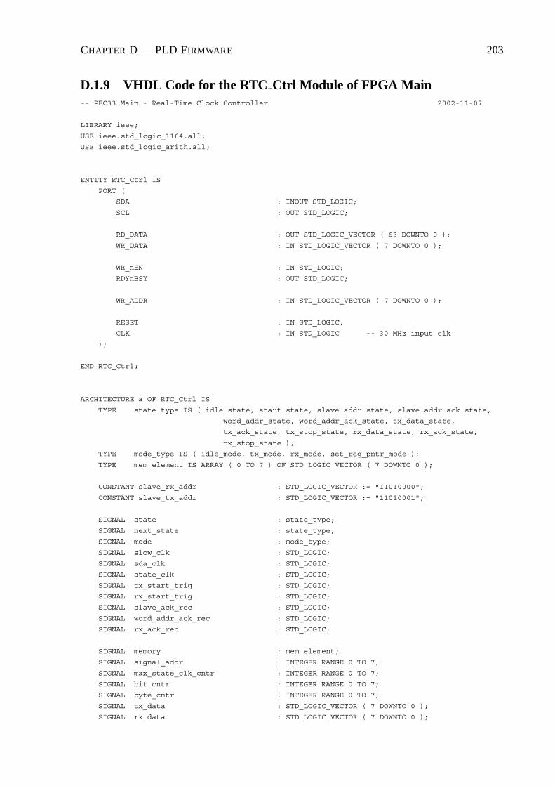
CHAPTER D — PLD FIRMWARE 203
D.1.9 VHDL Code for the RTC Ctrl Module of FPGA Main-- PEC33 Main - Real-Time Clock Controller 2002-11-07
LIBRARY ieee;
USE ieee.std_logic_1164.all;
USE ieee.std_logic_arith.all;
ENTITY RTC_Ctrl IS
PORT (
SDA : INOUT STD_LOGIC;
SCL : OUT STD_LOGIC;
RD_DATA : OUT STD_LOGIC_VECTOR ( 63 DOWNTO 0 );
WR_DATA : IN STD_LOGIC_VECTOR ( 7 DOWNTO 0 );
WR_nEN : IN STD_LOGIC;
RDYnBSY : OUT STD_LOGIC;
WR_ADDR : IN STD_LOGIC_VECTOR ( 7 DOWNTO 0 );
RESET : IN STD_LOGIC;
CLK : IN STD_LOGIC -- 30 MHz input clk
);
END RTC_Ctrl;
ARCHITECTURE a OF RTC_Ctrl IS
TYPE state_type IS ( idle_state, start_state, slave_addr_state, slave_addr_ack_state,
word_addr_state, word_addr_ack_state, tx_data_state,
tx_ack_state, tx_stop_state, rx_data_state, rx_ack_state,
rx_stop_state );
TYPE mode_type IS ( idle_mode, tx_mode, rx_mode, set_reg_pntr_mode );
TYPE mem_element IS ARRAY ( 0 TO 7 ) OF STD_LOGIC_VECTOR ( 7 DOWNTO 0 );
CONSTANT slave_rx_addr : STD_LOGIC_VECTOR := "11010000";
CONSTANT slave_tx_addr : STD_LOGIC_VECTOR := "11010001";
SIGNAL state : state_type;
SIGNAL next_state : state_type;
SIGNAL mode : mode_type;
SIGNAL slow_clk : STD_LOGIC;
SIGNAL sda_clk : STD_LOGIC;
SIGNAL state_clk : STD_LOGIC;
SIGNAL tx_start_trig : STD_LOGIC;
SIGNAL rx_start_trig : STD_LOGIC;
SIGNAL slave_ack_rec : STD_LOGIC;
SIGNAL word_addr_ack_rec : STD_LOGIC;
SIGNAL rx_ack_rec : STD_LOGIC;
SIGNAL memory : mem_element;
SIGNAL signal_addr : INTEGER RANGE 0 TO 7;
SIGNAL max_state_clk_cntr : INTEGER RANGE 0 TO 7;
SIGNAL bit_cntr : INTEGER RANGE 0 TO 7;
SIGNAL byte_cntr : INTEGER RANGE 0 TO 7;
SIGNAL tx_data : STD_LOGIC_VECTOR ( 7 DOWNTO 0 );
SIGNAL rx_data : STD_LOGIC_VECTOR ( 7 DOWNTO 0 );
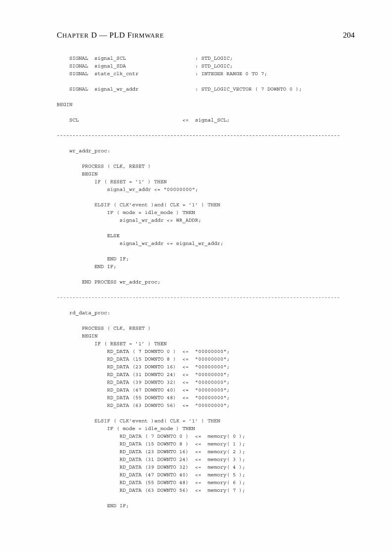
CHAPTER D — PLD FIRMWARE 204
SIGNAL signal_SCL : STD_LOGIC;
SIGNAL signal_SDA : STD_LOGIC;
SIGNAL state_clk_cntr : INTEGER RANGE 0 TO 7;
SIGNAL signal_wr_addr : STD_LOGIC_VECTOR ( 7 DOWNTO 0 );
BEGIN
SCL <= signal_SCL;
------------------------------------------------------------------------------------------
wr_addr_proc:
PROCESS ( CLK, RESET )
BEGIN
IF ( RESET = ’1’ ) THEN
signal_wr_addr <= "00000000";
ELSIF ( CLK’event )and( CLK = ’1’ ) THEN
IF ( mode = idle_mode ) THEN
signal_wr_addr <= WR_ADDR;
ELSE
signal_wr_addr <= signal_wr_addr;
END IF;
END IF;
END PROCESS wr_addr_proc;
------------------------------------------------------------------------------------------
rd_data_proc:
PROCESS ( CLK, RESET )
BEGIN
IF ( RESET = ’1’ ) THEN
RD_DATA ( 7 DOWNTO 0 ) <= "00000000";
RD_DATA (15 DOWNTO 8 ) <= "00000000";
RD_DATA (23 DOWNTO 16) <= "00000000";
RD_DATA (31 DOWNTO 24) <= "00000000";
RD_DATA (39 DOWNTO 32) <= "00000000";
RD_DATA (47 DOWNTO 40) <= "00000000";
RD_DATA (55 DOWNTO 48) <= "00000000";
RD_DATA (63 DOWNTO 56) <= "00000000";
ELSIF ( CLK’event )and( CLK = ’1’ ) THEN
IF ( mode = idle_mode ) THEN
RD_DATA ( 7 DOWNTO 0 ) <= memory( 0 );
RD_DATA (15 DOWNTO 8 ) <= memory( 1 );
RD_DATA (23 DOWNTO 16) <= memory( 2 );
RD_DATA (31 DOWNTO 24) <= memory( 3 );
RD_DATA (39 DOWNTO 32) <= memory( 4 );
RD_DATA (47 DOWNTO 40) <= memory( 5 );
RD_DATA (55 DOWNTO 48) <= memory( 6 );
RD_DATA (63 DOWNTO 56) <= memory( 7 );
END IF;

CHAPTER D — PLD FIRMWARE 205
END IF;
END PROCESS rd_data_proc;
------------------------------------------------------------------------------------------
rdynbsy_proc:
PROCESS ( CLK, RESET )
BEGIN
IF ( RESET = ’1’ ) THEN
RDYnBSY <= ’1’;
ELSIF ( CLK’event )and( CLK = ’1’ ) THEN
IF ( mode = idle_mode ) THEN
RDYnBSY <= ’1’;
ELSE
RDYnBSY <= ’0’;
END IF;
END IF;
END PROCESS rdynbsy_proc;
------------------------------------------------------------------------------------------
scl_proc:
PROCESS ( CLK, RESET, state )
BEGIN
IF ( RESET = ’1’ )or( state = idle_state ) THEN
signal_SCL <= ’1’;
ELSIF ( CLK’event )and( CLK = ’1’ ) THEN
IF ( state /= idle_state )and( state /= start_state ) THEN
signal_SCL <= slow_clk;
ELSE
signal_SCL <= ’1’;
END IF;
END IF;
END PROCESS scl_proc;
------------------------------------------------------------------------------------------
state_clk_proc:
PROCESS ( CLK, RESET, state )
BEGIN
IF ( RESET = ’1’ )or( state = idle_state ) THEN
state_clk <= ’1’;
ELSIF ( CLK’event )and( CLK = ’1’ ) THEN
IF ( state /= idle_state )and( state /= start_state )and
( state /= rx_stop_state )and( state /= tx_stop_state ) THEN
state_clk <= sda_clk;

CHAPTER D — PLD FIRMWARE 206
ELSE
state_clk <= ’1’;
END IF;
END IF;
END PROCESS state_clk_proc;
------------------------------------------------------------------------------------------
memory_proc:
PROCESS ( CLK, RESET )
BEGIN
IF ( RESET = ’1’ ) THEN
memory( 0 ) <= "00000000";
memory( 1 ) <= "00000000";
memory( 2 ) <= "00000000";
memory( 3 ) <= "00000000";
memory( 4 ) <= "00000000";
memory( 5 ) <= "00000000";
memory( 6 ) <= "00000000";
memory( 7 ) <= "00000000";
ELSIF ( CLK’event )and( CLK = ’1’ ) THEN
IF ( state = rx_ack_state ) THEN
memory ( byte_cntr ) <= rx_data;
ELSE
memory <= memory;
END IF;
END IF;
END PROCESS memory_proc;
------------------------------------------------------------------------------------------
slave_ack_proc:
PROCESS ( signal_scl, RESET, state )
BEGIN
IF ( RESET = ’1’ )or( state = idle_state ) THEN
slave_ack_rec <= ’0’;
ELSIF ( signal_scl’event )and( signal_scl = ’1’ ) THEN
IF ( state = slave_addr_ack_state ) THEN
slave_ack_rec <= not SDA;
ELSE
slave_ack_rec <= ’0’;
END IF;
END IF;
END PROCESS slave_ack_proc;
------------------------------------------------------------------------------------------
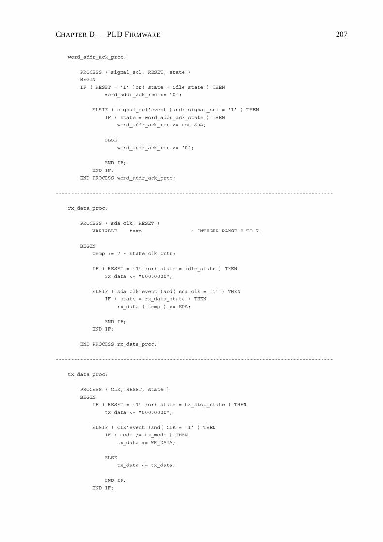
CHAPTER D — PLD FIRMWARE 207
word_addr_ack_proc:
PROCESS ( signal_scl, RESET, state )
BEGIN
IF ( RESET = ’1’ )or( state = idle_state ) THEN
word_addr_ack_rec <= ’0’;
ELSIF ( signal_scl’event )and( signal_scl = ’1’ ) THEN
IF ( state = word_addr_ack_state ) THEN
word_addr_ack_rec <= not SDA;
ELSE
word_addr_ack_rec <= ’0’;
END IF;
END IF;
END PROCESS word_addr_ack_proc;
------------------------------------------------------------------------------------------
rx_data_proc:
PROCESS ( sda_clk, RESET )
VARIABLE temp : INTEGER RANGE 0 TO 7;
BEGIN
temp := 7 - state_clk_cntr;
IF ( RESET = ’1’ )or( state = idle_state ) THEN
rx_data <= "00000000";
ELSIF ( sda_clk’event )and( sda_clk = ’1’ ) THEN
IF ( state = rx_data_state ) THEN
rx_data ( temp ) <= SDA;
END IF;
END IF;
END PROCESS rx_data_proc;
------------------------------------------------------------------------------------------
tx_data_proc:
PROCESS ( CLK, RESET, state )
BEGIN
IF ( RESET = ’1’ )or( state = tx_stop_state ) THEN
tx_data <= "00000000";
ELSIF ( CLK’event )and( CLK = ’1’ ) THEN
IF ( mode /= tx_mode ) THEN
tx_data <= WR_DATA;
ELSE
tx_data <= tx_data;
END IF;
END IF;

CHAPTER D — PLD FIRMWARE 208
END PROCESS tx_data_proc;
------------------------------------------------------------------------------------------
sda_proc:
PROCESS ( sda_clk, RESET )
VARIABLE temp : STD_LOGIC;
BEGIN
IF ( state = idle_state )or( state = slave_addr_ack_state )or
( state = word_addr_ack_state )or( state = tx_ack_state )or
( temp = ’1’ ) THEN
SDA <= ’Z’;
ELSE
SDA <= signal_SDA;
END IF;
IF ( RESET = ’1’ ) THEN
signal_SDA <= ’1’;
temp := ’0’;
ELSIF ( sda_clk’event )and( sda_clk = ’0’ ) THEN
IF ( state = idle_state ) THEN
signal_SDA <= ’1’;
temp := ’0’;
ELSIF ( state = start_state ) THEN
signal_SDA <= ’0’;
temp := ’0’;
ELSIF ( state = slave_addr_state )and( mode = rx_mode ) THEN
signal_SDA <= slave_tx_addr( bit_cntr );
temp := ’0’;
ELSIF ( state = slave_addr_state ) THEN
signal_SDA <= slave_rx_addr( bit_cntr );
temp := ’0’;
ELSIF ( state = slave_addr_ack_state ) THEN
signal_SDA <= ’0’;
temp := ’0’;
ELSIF ( state = word_addr_state ) THEN
IF ( mode = tx_mode ) THEN
signal_SDA <= signal_wr_addr( bit_cntr );
ELSE
signal_SDA <= ’0’;
END IF;
temp := ’0’;
ELSIF ( state = word_addr_ack_state ) THEN
signal_SDA <= ’0’;
temp := ’0’;
ELSIF ( state = tx_ack_state ) THEN
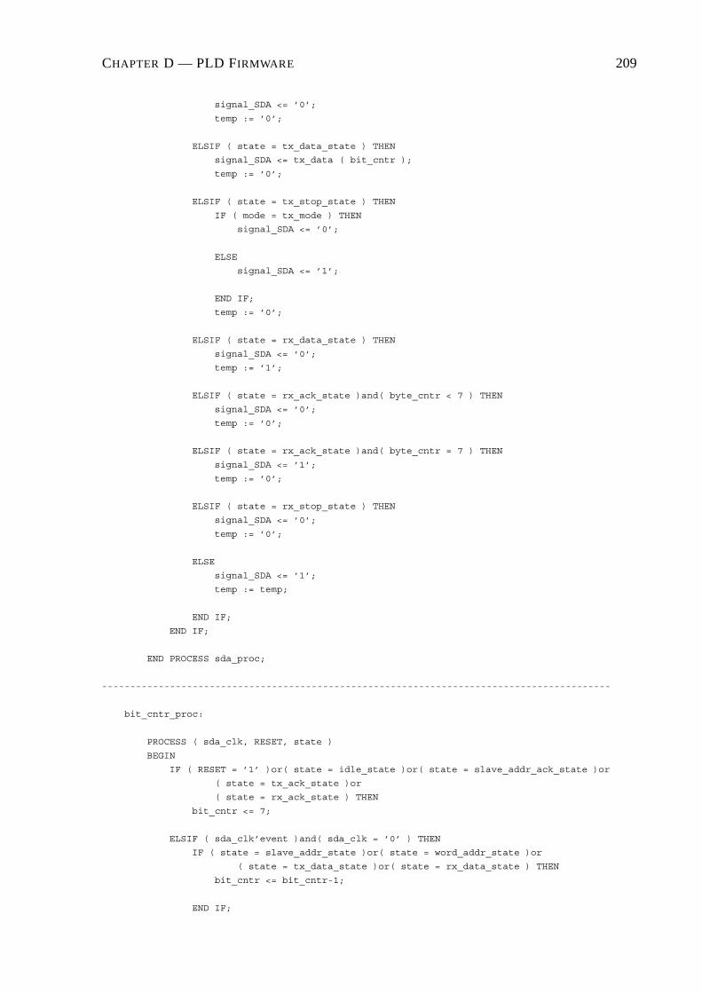
CHAPTER D — PLD FIRMWARE 209
signal_SDA <= ’0’;
temp := ’0’;
ELSIF ( state = tx_data_state ) THEN
signal_SDA <= tx_data ( bit_cntr );
temp := ’0’;
ELSIF ( state = tx_stop_state ) THEN
IF ( mode = tx_mode ) THEN
signal_SDA <= ’0’;
ELSE
signal_SDA <= ’1’;
END IF;
temp := ’0’;
ELSIF ( state = rx_data_state ) THEN
signal_SDA <= ’0’;
temp := ’1’;
ELSIF ( state = rx_ack_state )and( byte_cntr < 7 ) THEN
signal_SDA <= ’0’;
temp := ’0’;
ELSIF ( state = rx_ack_state )and( byte_cntr = 7 ) THEN
signal_SDA <= ’1’;
temp := ’0’;
ELSIF ( state = rx_stop_state ) THEN
signal_SDA <= ’0’;
temp := ’0’;
ELSE
signal_SDA <= ’1’;
temp := temp;
END IF;
END IF;
END PROCESS sda_proc;
------------------------------------------------------------------------------------------
bit_cntr_proc:
PROCESS ( sda_clk, RESET, state )
BEGIN
IF ( RESET = ’1’ )or( state = idle_state )or( state = slave_addr_ack_state )or
( state = tx_ack_state )or
( state = rx_ack_state ) THEN
bit_cntr <= 7;
ELSIF ( sda_clk’event )and( sda_clk = ’0’ ) THEN
IF ( state = slave_addr_state )or( state = word_addr_state )or
( state = tx_data_state )or( state = rx_data_state ) THEN
bit_cntr <= bit_cntr-1;
END IF;
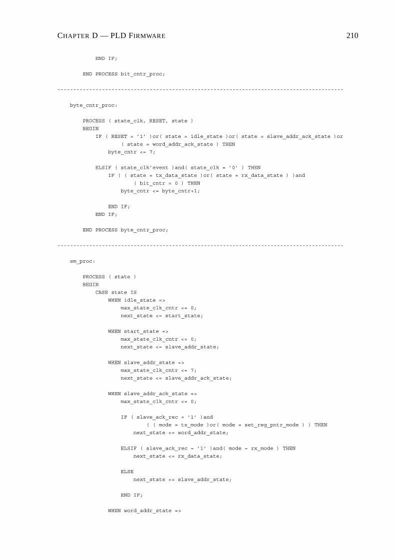
CHAPTER D — PLD FIRMWARE 210
END IF;
END PROCESS bit_cntr_proc;
------------------------------------------------------------------------------------------
byte_cntr_proc:
PROCESS ( state_clk, RESET, state )
BEGIN
IF ( RESET = ’1’ )or( state = idle_state )or( state = slave_addr_ack_state )or
( state = word_addr_ack_state ) THEN
byte_cntr <= 7;
ELSIF ( state_clk’event )and( state_clk = ’0’ ) THEN
IF ( ( state = tx_data_state )or( state = rx_data_state ) )and
( bit_cntr = 0 ) THEN
byte_cntr <= byte_cntr+1;
END IF;
END IF;
END PROCESS byte_cntr_proc;
------------------------------------------------------------------------------------------
sm_proc:
PROCESS ( state )
BEGIN
CASE state IS
WHEN idle_state =>
max_state_clk_cntr <= 0;
next_state <= start_state;
WHEN start_state =>
max_state_clk_cntr <= 0;
next_state <= slave_addr_state;
WHEN slave_addr_state =>
max_state_clk_cntr <= 7;
next_state <= slave_addr_ack_state;
WHEN slave_addr_ack_state =>
max_state_clk_cntr <= 0;
IF ( slave_ack_rec = ’1’ )and
( ( mode = tx_mode )or( mode = set_reg_pntr_mode ) ) THEN
next_state <= word_addr_state;
ELSIF ( slave_ack_rec = ’1’ )and( mode = rx_mode ) THEN
next_state <= rx_data_state;
ELSE
next_state <= slave_addr_state;
END IF;
WHEN word_addr_state =>

CHAPTER D — PLD FIRMWARE 211
max_state_clk_cntr <= 7;
next_state <= word_addr_ack_state;
WHEN word_addr_ack_state =>
max_state_clk_cntr <= 0;
IF ( mode = tx_mode ) THEN
next_state <= tx_data_state;
ELSIF ( mode = set_reg_pntr_mode ) THEN
next_state <= tx_stop_state;
ELSE
next_state <= word_addr_state;
END IF;
WHEN tx_data_state =>
max_state_clk_cntr <= 7;
next_state <= tx_ack_state;
WHEN tx_ack_state =>
max_state_clk_cntr <= 0;
next_state <= tx_stop_state;
WHEN tx_stop_state =>
max_state_clk_cntr <= 0;
IF ( mode = tx_mode ) THEN
next_state <= idle_state;
ELSE
next_state <= start_state;
END IF;
WHEN rx_data_state =>
max_state_clk_cntr <= 7;
next_state <= rx_ack_state;
WHEN rx_ack_state =>
max_state_clk_cntr <= 0;
IF ( byte_cntr = 7 ) THEN
next_state <= rx_stop_state;
ELSE
next_state <= rx_data_state;
END IF;
WHEN rx_stop_state =>
max_state_clk_cntr <= 0;
next_state <= idle_state;
WHEN others =>
max_state_clk_cntr <= max_state_clk_cntr;
next_state <= next_state;

CHAPTER D — PLD FIRMWARE 212
END CASE;
END PROCESS sm_proc;
------------------------------------------------------------------------------------------
sm_ctrl_proc:
PROCESS ( slow_clk, RESET )
BEGIN
IF ( RESET = ’1’ ) THEN
state <= idle_state;
state_clk_cntr <= 0;
ELSIF ( slow_clk’event )and( slow_clk = ’0’ ) THEN
IF ( ( ( tx_start_trig = ’1’ )or( rx_start_trig = ’1’ ) )and
( state = idle_state ) ) THEN
state <= start_state;
state_clk_cntr <= 0;
ELSIF ( state_clk_cntr = max_state_clk_cntr )and( state /= idle_state ) THEN
state <= next_state;
state_clk_cntr <= 0;
ELSIF ( state_clk_cntr /= max_state_clk_cntr )and( state /= idle_state ) THEN
state <= state;
state_clk_cntr <= state_clk_cntr + 1;
ELSE
state <= state;
state_clk_cntr <= state_clk_cntr;
END IF;
END IF;
END PROCESS sm_ctrl_proc;
------------------------------------------------------------------------------------------
tx_start_trig_proc:
PROCESS ( WR_nEN, RESET, state )
BEGIN
IF ( RESET = ’1’ )or( ( state = tx_stop_state )and( mode = tx_mode ) ) THEN
tx_start_trig <= ’0’;
ELSIF ( WR_nEN’event )and( WR_nEN = ’1’ ) THEN
tx_start_trig <= ’1’;
END IF;
END PROCESS tx_start_trig_proc;
------------------------------------------------------------------------------------------
rx_start_proc:
PROCESS ( CLK, RESET, state )
VARIABLE update_cntr : INTEGER RANGE 0 TO 30000000;
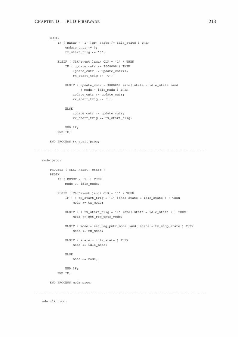
CHAPTER D — PLD FIRMWARE 213
BEGIN
IF ( RESET = ’1’ )or( state /= idle_state ) THEN
update_cntr := 0;
rx_start_trig <= ’0’;
ELSIF ( CLK’event )and( CLK = ’1’ ) THEN
IF ( update_cntr /= 3000000 ) THEN
update_cntr := update_cntr+1;
rx_start_trig <= ’0’;
ELSIF ( update_cntr = 3000000 )and( state = idle_state )and
( mode = idle_mode ) THEN
update_cntr := update_cntr;
rx_start_trig <= ’1’;
ELSE
update_cntr := update_cntr;
rx_start_trig <= rx_start_trig;
END IF;
END IF;
END PROCESS rx_start_proc;
------------------------------------------------------------------------------------------
mode_proc:
PROCESS ( CLK, RESET, state )
BEGIN
IF ( RESET = ’1’ ) THEN
mode <= idle_mode;
ELSIF ( CLK’event )and( CLK = ’1’ ) THEN
IF ( ( tx_start_trig = ’1’ )and( state = idle_state ) ) THEN
mode <= tx_mode;
ELSIF ( ( rx_start_trig = ’1’ )and( state = idle_state ) ) THEN
mode <= set_reg_pntr_mode;
ELSIF ( mode = set_reg_pntr_mode )and( state = tx_stop_state ) THEN
mode <= rx_mode;
ELSIF ( state = idle_state ) THEN
mode <= idle_mode;
ELSE
mode <= mode;
END IF;
END IF;
END PROCESS mode_proc;
------------------------------------------------------------------------------------------
sda_clk_proc:

CHAPTER D — PLD FIRMWARE 214
PROCESS ( CLK, RESET )
VARIABLE sda_clk_cntr : INTEGER RANGE 0 TO 150;
BEGIN
IF ( RESET = ’1’ ) THEN
sda_clk_cntr := 75;
sda_clk <= ’0’;
ELSIF ( CLK’event )and( CLK = ’1’ ) THEN
IF ( sda_clk_cntr < 150 ) THEN
sda_clk <= sda_clk;
sda_clk_cntr := sda_clk_cntr + 1;
ELSE
sda_clk <= not sda_clk;
sda_clk_cntr := 0;
END IF;
END IF;
END PROCESS sda_clk_proc;
------------------------------------------------------------------------------------------
slow_clk_proc:
PROCESS ( CLK, RESET )
VARIABLE slow_clk_cntr : INTEGER RANGE 0 TO 150;
BEGIN
IF ( RESET = ’1’ ) THEN
slow_clk_cntr := 0;
slow_clk <= ’1’;
ELSIF ( CLK’event )and( CLK = ’1’ ) THEN
IF ( slow_clk_cntr < 150 ) THEN
slow_clk <= slow_clk;
slow_clk_cntr := slow_clk_cntr + 1;
ELSE
slow_clk <= not slow_clk;
slow_clk_cntr := 0;
END IF;
END IF;
END PROCESS slow_clk_proc;
END a;

CHAPTER D — PLD FIRMWARE 215
D.1.10 Graphical Design File for the SP Ctrl Module of FPGA Main
GLOBAL_RESETGLOBAL_CLK
SP_BAUDRATE[2..0]SP_DATA_SENT
SP_TX_DATA_RDYSP_TX_DATA[7..0]
TX_RDY
SP_RX_DATA[7..0]SP_DATA_REC
GLOBAL_RESET
SP_TX_DATA_RDYSP_TX_DATA[7..0]
SP_TX_RDYnBSY
TX_RDYSP_DATA_SENT
GLOBAL_CLKGLOBAL_RESETSP_DATA_RECSP_RX_DATA[7..0]
SP_BAUDRATE[2..0]INPUT
GLOBAL_RESETINPUT
GLOBAL_CLKINPUT
SP_RX INPUT
SP_TXOUTPUT
DSP_H1 INPUT
DSP_CLKX0INPUT
DSP_FSX0INPUT
DSP_DX0 INPUT
SP_TX_RDYnBSYOUTPUT
DSP_CLKR0OUTPUTDSP_FSR0OUTPUTDSP_DR0OUTPUT
Figure D.4: Graphical Design File of the SP Ctrl Symbol

CHAPTER D — PLD FIRMWARE 216
D.1.11 VHDL Code for the UART Ctrl Module of FPGA Main-- PEC33 Main - UART Controller 2002-11-07
LIBRARY ieee;
USE ieee.std_logic_1164.all;
USE ieee.std_logic_arith.all;
-- Word Length: 8
-- Parity: Even
-- -------------------------------------------
-- | Baudrate | Baudrate | CLK Constant |
-- | | Input | for 30 MHz |
-- -------------------------------------------
-- -------------------------------------------
-- | 1200 | 001 | 1562 |
-- | 2400 | 010 | 781 |
-- | 9600 |000 or 011 | 195 |
-- | 19200 | 100 | 98 |
-- -------------------------------------------
ENTITY UART_Ctrl IS
PORT (
RX_DATA_IN : IN STD_LOGIC;
RX_DATA_OUT : OUT STD_LOGIC_VECTOR( 7 DOWNTO 0 );
DATA_REC : OUT STD_LOGIC;
TX_DATA_IN : IN STD_LOGIC_VECTOR( 7 DOWNTO 0 );
TX_DATA_OUT : OUT STD_LOGIC;
TX_DATA_RDY : IN STD_LOGIC;
TX_RDY : OUT STD_LOGIC;
DATA_SENT : OUT STD_LOGIC;
BAUDRATE : IN STD_LOGIC_VECTOR( 2 DOWNTO 0 );
RESET : IN STD_LOGIC;
CLK : IN STD_LOGIC -- 30 kHz input clk
);
END UART_Ctrl;
ARCHITECTURE a OF UART_Ctrl IS
TYPE rx_state_type IS ( idle_state, start_state, sampling_state, parity_state,
stop_state );
TYPE tx_state_type IS ( idle_state, start_state, tx_data_state, parity_state,
stop_state );
-- oversampling clk - Freq = 16 x baudrate
SIGNAL baud_clk : STD_LOGIC;
-- Counter dividing CLK to get baud_clk
SIGNAL max_baud_cntr : INTEGER RANGE 0 TO 8191;
SIGNAL halfmax_baud_cntr : INTEGER RANGE 0 TO 8191;
SIGNAL error_reg : STD_LOGIC_VECTOR ( 1 DOWNTO 0 );

CHAPTER D — PLD FIRMWARE 217
SIGNAL rx_state : rx_state_type;
SIGNAL next_rx_state : rx_state_type;
SIGNAL rx_bit_cntr : INTEGER RANGE 0 TO 8;
-- RX oversampling counter
SIGNAL rx_os_cntr : INTEGER RANGE 0 TO 15;
SIGNAL rx_os_cntr_trigval : INTEGER RANGE 0 TO 15;
SIGNAL rx_sample_data : STD_LOGIC_VECTOR ( 8 DOWNTO 0 );
SIGNAL rx_parity : STD_LOGIC;
SIGNAL rx_parity_chk : STD_LOGIC;
SIGNAL stopbit : STD_LOGIC;
SIGNAL rx_start_trig : STD_LOGIC;
SIGNAL tx_state : tx_state_type;
SIGNAL next_tx_state : tx_state_type;
SIGNAL tx_bit_cntr : INTEGER RANGE 0 TO 8;
-- TX oversampling counter
SIGNAL tx_os_cntr : INTEGER RANGE 0 TO 15;
SIGNAL tx_sample_data : STD_LOGIC_VECTOR ( 8 DOWNTO 0 );
SIGNAL tx_parity : STD_LOGIC;
SIGNAL tx_start_trig : STD_LOGIC;
SIGNAL new_tx_data : STD_LOGIC_VECTOR ( 7 DOWNTO 0 );
SIGNAL new_rx_data : STD_LOGIC_VECTOR ( 7 DOWNTO 0 );
SIGNAL rx_sent : STD_LOGIC;
SIGNAL baud_cntr : INTEGER RANGE 0 TO 8191;
BEGIN
TX_RDY <= ’1’ WHEN ( tx_state = idle_state ) ELSE
’0’;
RX_DATA_OUT <= new_rx_data;
DATA_SENT <= ’0’ WHEN ( RESET = ’1’ ) ELSE
’1’ WHEN ( tx_state = stop_state ) ELSE
’0’ WHEN ( tx_state = start_state )or
( tx_state = tx_data_state );
max_baud_cntr <= 195 WHEN ( BAUDRATE = "000" ) ELSE
1562 WHEN ( BAUDRATE = "001" ) ELSE
781 WHEN ( BAUDRATE = "010" ) ELSE
195 WHEN ( BAUDRATE = "011" ) ELSE
98 WHEN ( BAUDRATE = "100" ) ELSE
781;
halfmax_baud_cntr <= 97 WHEN ( BAUDRATE = "000" ) ELSE
781 WHEN ( BAUDRATE = "001" ) ELSE
390 WHEN ( BAUDRATE = "010" ) ELSE
97 WHEN ( BAUDRATE = "011" ) ELSE
49 WHEN ( BAUDRATE = "100" ) ELSE
390;
------------------------------------------------------------------------------------------
baudrate_proc:
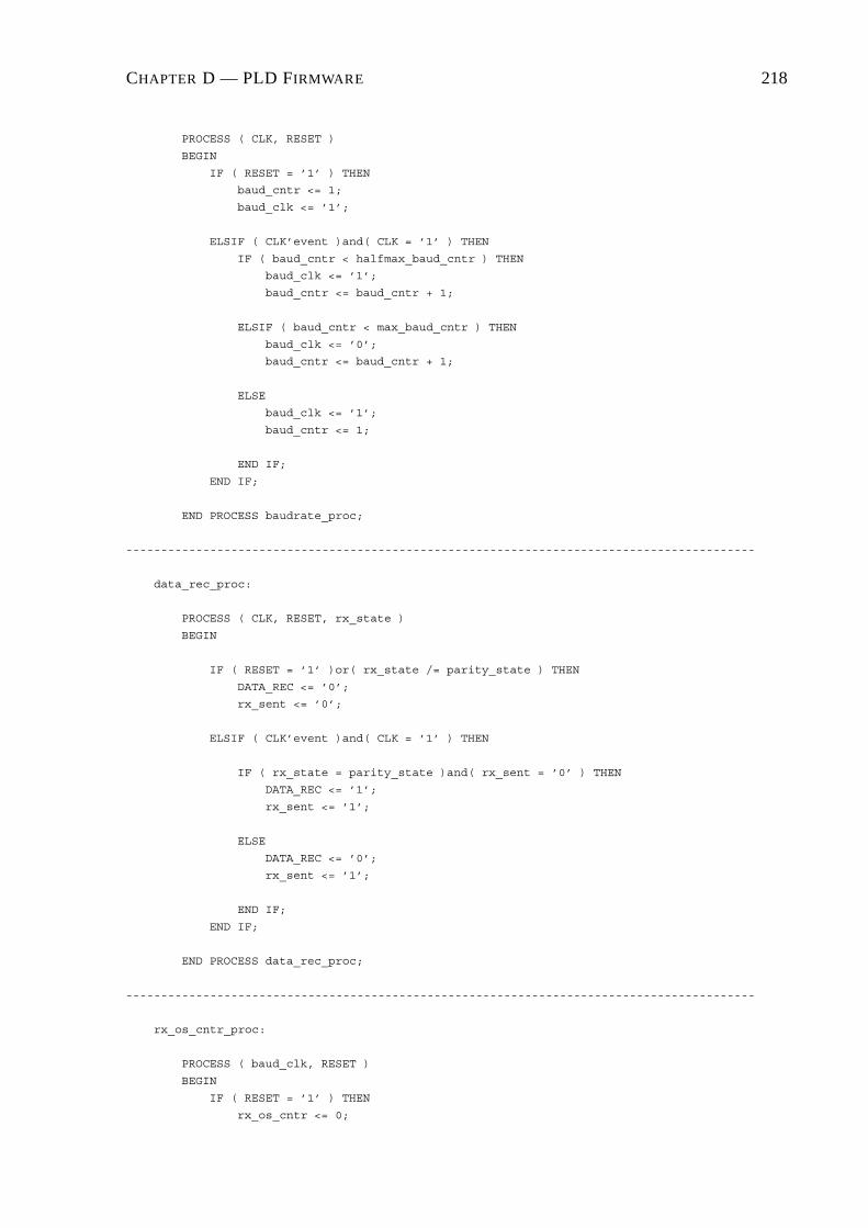
CHAPTER D — PLD FIRMWARE 218
PROCESS ( CLK, RESET )
BEGIN
IF ( RESET = ’1’ ) THEN
baud_cntr <= 1;
baud_clk <= ’1’;
ELSIF ( CLK’event )and( CLK = ’1’ ) THEN
IF ( baud_cntr < halfmax_baud_cntr ) THEN
baud_clk <= ’1’;
baud_cntr <= baud_cntr + 1;
ELSIF ( baud_cntr < max_baud_cntr ) THEN
baud_clk <= ’0’;
baud_cntr <= baud_cntr + 1;
ELSE
baud_clk <= ’1’;
baud_cntr <= 1;
END IF;
END IF;
END PROCESS baudrate_proc;
------------------------------------------------------------------------------------------
data_rec_proc:
PROCESS ( CLK, RESET, rx_state )
BEGIN
IF ( RESET = ’1’ )or( rx_state /= parity_state ) THEN
DATA_REC <= ’0’;
rx_sent <= ’0’;
ELSIF ( CLK’event )and( CLK = ’1’ ) THEN
IF ( rx_state = parity_state )and( rx_sent = ’0’ ) THEN
DATA_REC <= ’1’;
rx_sent <= ’1’;
ELSE
DATA_REC <= ’0’;
rx_sent <= ’1’;
END IF;
END IF;
END PROCESS data_rec_proc;
------------------------------------------------------------------------------------------
rx_os_cntr_proc:
PROCESS ( baud_clk, RESET )
BEGIN
IF ( RESET = ’1’ ) THEN
rx_os_cntr <= 0;
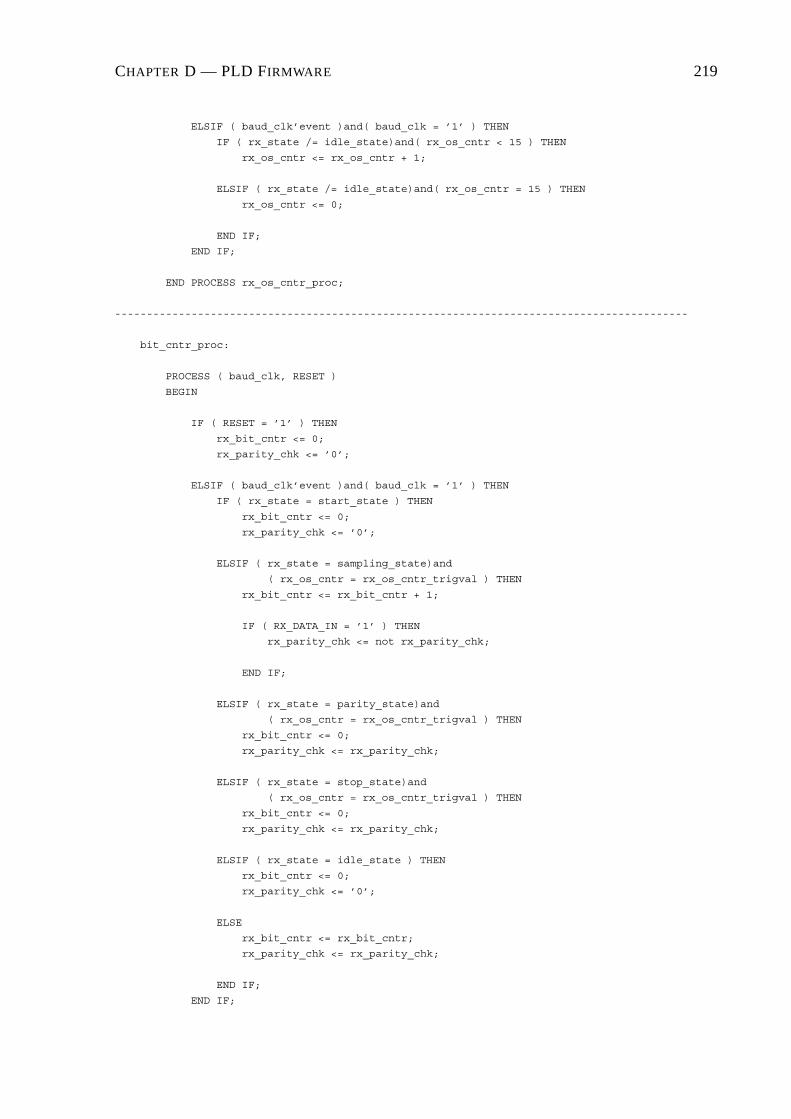
CHAPTER D — PLD FIRMWARE 219
ELSIF ( baud_clk’event )and( baud_clk = ’1’ ) THEN
IF ( rx_state /= idle_state)and( rx_os_cntr < 15 ) THEN
rx_os_cntr <= rx_os_cntr + 1;
ELSIF ( rx_state /= idle_state)and( rx_os_cntr = 15 ) THEN
rx_os_cntr <= 0;
END IF;
END IF;
END PROCESS rx_os_cntr_proc;
------------------------------------------------------------------------------------------
bit_cntr_proc:
PROCESS ( baud_clk, RESET )
BEGIN
IF ( RESET = ’1’ ) THEN
rx_bit_cntr <= 0;
rx_parity_chk <= ’0’;
ELSIF ( baud_clk’event )and( baud_clk = ’1’ ) THEN
IF ( rx_state = start_state ) THEN
rx_bit_cntr <= 0;
rx_parity_chk <= ’0’;
ELSIF ( rx_state = sampling_state)and
( rx_os_cntr = rx_os_cntr_trigval ) THEN
rx_bit_cntr <= rx_bit_cntr + 1;
IF ( RX_DATA_IN = ’1’ ) THEN
rx_parity_chk <= not rx_parity_chk;
END IF;
ELSIF ( rx_state = parity_state)and
( rx_os_cntr = rx_os_cntr_trigval ) THEN
rx_bit_cntr <= 0;
rx_parity_chk <= rx_parity_chk;
ELSIF ( rx_state = stop_state)and
( rx_os_cntr = rx_os_cntr_trigval ) THEN
rx_bit_cntr <= 0;
rx_parity_chk <= rx_parity_chk;
ELSIF ( rx_state = idle_state ) THEN
rx_bit_cntr <= 0;
rx_parity_chk <= ’0’;
ELSE
rx_bit_cntr <= rx_bit_cntr;
rx_parity_chk <= rx_parity_chk;
END IF;
END IF;

CHAPTER D — PLD FIRMWARE 220
END PROCESS bit_cntr_proc;
------------------------------------------------------------------------------------------
sample_bit_proc:
PROCESS ( CLK, RESET )
BEGIN
IF ( RESET = ’1’ ) THEN
rx_sample_data <= "000000000";
rx_parity <= ’0’;
stopbit <= ’0’;
error_reg <= "00";
ELSIF ( CLK’event )and( CLK = ’1’ ) THEN
IF ( rx_state = start_state ) THEN
rx_sample_data <= "000000000";
rx_parity <= ’0’;
stopbit <= ’0’;
error_reg <= "00";
ELSIF ( rx_state = sampling_state)and
( rx_os_cntr = rx_os_cntr_trigval ) THEN
rx_sample_data( rx_bit_cntr ) <= RX_DATA_IN;
rx_parity <= ’0’;
stopbit <= ’0’;
error_reg <= error_reg;
ELSIF ( rx_state = parity_state)and
( rx_os_cntr = rx_os_cntr_trigval ) THEN
rx_sample_data <= rx_sample_data;
rx_parity <= RX_DATA_IN;
stopbit <= ’0’;
error_reg(0) <= error_reg(0);
error_reg(1) <= error_reg(1);
ELSIF ( rx_state = stop_state)and
( rx_os_cntr = rx_os_cntr_trigval ) THEN
rx_sample_data <= rx_sample_data;
rx_parity <= rx_parity;
stopbit <= RX_DATA_IN;
error_reg(1) <= error_reg(1);
error_reg(0) <= ( rx_parity )xor( rx_parity_chk );
ELSIF ( rx_state = idle_state ) THEN
rx_sample_data <= rx_sample_data;
rx_parity <= rx_parity;
stopbit <= stopbit;
error_reg(1) <= not( stopbit );
error_reg(0) <= error_reg(0);
ELSE
rx_sample_data <= rx_sample_data;
rx_parity <= rx_parity;
stopbit <= stopbit;
error_reg <= error_reg;
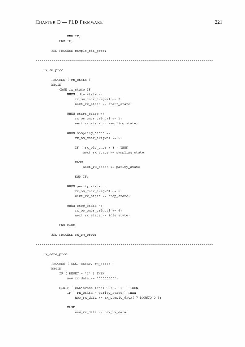
CHAPTER D — PLD FIRMWARE 221
END IF;
END IF;
END PROCESS sample_bit_proc;
------------------------------------------------------------------------------------------
rx_sm_proc:
PROCESS ( rx_state )
BEGIN
CASE rx_state IS
WHEN idle_state =>
rx_os_cntr_trigval <= 0;
next_rx_state <= start_state;
WHEN start_state =>
rx_os_cntr_trigval <= 1;
next_rx_state <= sampling_state;
WHEN sampling_state =>
rx_os_cntr_trigval <= 6;
IF ( rx_bit_cntr < 8 ) THEN
next_rx_state <= sampling_state;
ELSE
next_rx_state <= parity_state;
END IF;
WHEN parity_state =>
rx_os_cntr_trigval <= 6;
next_rx_state <= stop_state;
WHEN stop_state =>
rx_os_cntr_trigval <= 6;
next_rx_state <= idle_state;
END CASE;
END PROCESS rx_sm_proc;
------------------------------------------------------------------------------------------
rx_data_proc:
PROCESS ( CLK, RESET, rx_state )
BEGIN
IF ( RESET = ’1’ ) THEN
new_rx_data <= "00000000";
ELSIF ( CLK’event )and( CLK = ’1’ ) THEN
IF ( rx_state = parity_state ) THEN
new_rx_data <= rx_sample_data( 7 DOWNTO 0 );
ELSE
new_rx_data <= new_rx_data;

CHAPTER D — PLD FIRMWARE 222
END IF;
END IF;
END PROCESS rx_data_proc;
------------------------------------------------------------------------------------------
rx_sm_ctrl_proc:
PROCESS ( baud_CLK, RESET )
BEGIN
IF ( RESET = ’1’ ) THEN
rx_state <= idle_state;
ELSIF ( baud_CLK’event )and( baud_CLK = ’1’ ) THEN
IF ( rx_start_trig = ’1’ )and( rx_state = idle_state ) THEN
rx_state <= next_rx_state;
ELSIF ( rx_state /= idle_state)and( rx_os_cntr = 15 ) THEN
rx_state <= next_rx_state;
ELSE
rx_state <= rx_state;
END IF;
END IF;
END PROCESS rx_sm_ctrl_proc;
------------------------------------------------------------------------------------------
rx_start_proc:
PROCESS ( RX_DATA_IN, RESET )
BEGIN
IF ( RESET = ’1’ )or
( ( rx_state /= idle_state )and( rx_state /= stop_state ) ) THEN
rx_start_trig <= ’0’;
ELSIF ( RX_DATA_IN’event )and( RX_DATA_IN = ’0’ ) THEN
IF ( rx_state = idle_state )or( rx_state = stop_state ) THEN
rx_start_trig <= ’1’;
ELSE
rx_start_trig <= ’0’;
END IF;
END IF;
END PROCESS rx_start_proc;
------------------------------------------------------------------------------------------
tx_os_cntr_proc:
PROCESS ( baud_clk, RESET )
BEGIN
IF ( RESET = ’1’ ) THEN
tx_os_cntr <= 0;

CHAPTER D — PLD FIRMWARE 223
ELSIF ( baud_clk’event )and( baud_clk = ’1’ ) THEN
IF ( tx_state /= idle_state)and( tx_os_cntr < 15 ) THEN
tx_os_cntr <= tx_os_cntr + 1;
ELSIF ( tx_state /= idle_state)and( tx_os_cntr = 15 ) THEN
tx_os_cntr <= 0;
END IF;
END IF;
END PROCESS tx_os_cntr_proc;
------------------------------------------------------------------------------------------
send_bit_proc:
PROCESS ( baud_clk, RESET )
BEGIN
IF ( RESET = ’1’ ) THEN
tx_bit_cntr <= 0;
tx_parity <= ’0’;
TX_DATA_OUT <= ’1’;
ELSIF ( baud_clk’event )and( baud_clk = ’1’ ) THEN
IF ( tx_state = start_state ) THEN
tx_parity <= ’0’;
TX_DATA_OUT <= ’0’;
ELSIF ( tx_state = tx_data_state )and( tx_os_cntr = 0 ) THEN
TX_DATA_OUT <= tx_sample_data( tx_bit_cntr );
IF ( tx_sample_data( tx_bit_cntr ) = ’1’ ) THEN
tx_parity <= not tx_parity;
END IF;
tx_bit_cntr <= tx_bit_cntr + 1;
ELSIF ( tx_state = parity_state)and( tx_os_cntr = 0 ) THEN
tx_parity <= tx_parity;
tx_bit_cntr <= 0;
TX_DATA_OUT <= tx_parity;
ELSIF ( tx_state = stop_state) THEN
tx_parity <= tx_parity;
tx_bit_cntr <= 0;
TX_DATA_OUT <= ’1’;
ELSIF ( tx_state = idle_state ) THEN
tx_parity <= ’0’;
tx_bit_cntr <= 0;
TX_DATA_OUT <= ’1’;
ELSE
tx_bit_cntr <= tx_bit_cntr;
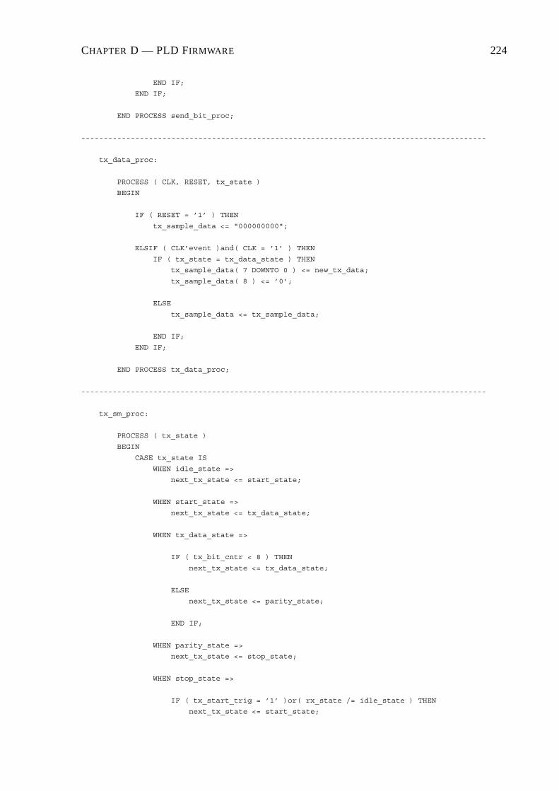
CHAPTER D — PLD FIRMWARE 224
END IF;
END IF;
END PROCESS send_bit_proc;
------------------------------------------------------------------------------------------
tx_data_proc:
PROCESS ( CLK, RESET, tx_state )
BEGIN
IF ( RESET = ’1’ ) THEN
tx_sample_data <= "000000000";
ELSIF ( CLK’event )and( CLK = ’1’ ) THEN
IF ( tx_state = tx_data_state ) THEN
tx_sample_data( 7 DOWNTO 0 ) <= new_tx_data;
tx_sample_data( 8 ) <= ’0’;
ELSE
tx_sample_data <= tx_sample_data;
END IF;
END IF;
END PROCESS tx_data_proc;
------------------------------------------------------------------------------------------
tx_sm_proc:
PROCESS ( tx_state )
BEGIN
CASE tx_state IS
WHEN idle_state =>
next_tx_state <= start_state;
WHEN start_state =>
next_tx_state <= tx_data_state;
WHEN tx_data_state =>
IF ( tx_bit_cntr < 8 ) THEN
next_tx_state <= tx_data_state;
ELSE
next_tx_state <= parity_state;
END IF;
WHEN parity_state =>
next_tx_state <= stop_state;
WHEN stop_state =>
IF ( tx_start_trig = ’1’ )or( rx_state /= idle_state ) THEN
next_tx_state <= start_state;

CHAPTER D — PLD FIRMWARE 225
ELSE
next_tx_state <= idle_state;
END IF;
END CASE;
END PROCESS tx_sm_proc;
------------------------------------------------------------------------------------------
tx_sm_ctrl_proc:
PROCESS ( baud_CLK, RESET )
BEGIN
IF ( RESET = ’1’ ) THEN
tx_state <= idle_state;
ELSIF ( baud_CLK’event )and( baud_CLK = ’1’ ) THEN
IF ( tx_start_trig = ’1’ )and( tx_state = idle_state ) THEN
tx_state <= next_tx_state;
ELSIF ( tx_state /= idle_state)and( tx_os_cntr = 15 ) THEN
tx_state <= next_tx_state;
ELSE
tx_state <= tx_state;
END IF;
END IF;
END PROCESS tx_sm_ctrl_proc;
------------------------------------------------------------------------------------------
tx_start_proc:
PROCESS ( TX_DATA_RDY, RESET, tx_state )
BEGIN
IF ( RESET = ’1’ )or( tx_state = start_state ) THEN
tx_start_trig <= ’0’;
ELSIF ( TX_DATA_RDY’event )and( TX_DATA_RDY = ’0’ ) THEN
tx_start_trig <= ’1’;
END IF;
END PROCESS tx_start_proc;
------------------------------------------------------------------------------------------
new_tx_data_proc:
PROCESS ( TX_DATA_RDY, RESET )
BEGIN

CHAPTER D — PLD FIRMWARE 226
IF ( RESET = ’1’ ) THEN
new_tx_data <= "00000000";
ELSIF ( TX_DATA_RDY’event )and( TX_DATA_RDY = ’0’ ) THEN
new_tx_data <= TX_DATA_IN;
END IF;
END PROCESS new_tx_data_proc;
END a;

CHAPTER D — PLD FIRMWARE 227
D.1.12 VHDL Code for the DSP SP TX Ctrl Module of FPGA Main-- PEC33 Main - TX interface between the DSP and the UART 2002-11-07
LIBRARY ieee;
USE ieee.std_logic_1164.all;
USE ieee.std_logic_arith.all;
-- TX Input Word Length: 8 Bits
-- TX Output Word Length: 8 Bits
ENTITY DSP_SP_TX_Ctrl IS
PORT(
DATA_OUT : OUT STD_LOGIC_VECTOR( 7 DOWNTO 0 );
TX_DATA_RDY : OUT STD_LOGIC;
DATA_SENT : IN STD_LOGIC;
TX_RDY : IN STD_LOGIC;
RDYnBSY : OUT STD_LOGIC;
DX0 : IN STD_LOGIC;
FSX0 : IN STD_LOGIC;
CLKX0 : IN STD_LOGIC;
RESET : IN STD_LOGIC;
CLK : IN STD_LOGIC
);
END DSP_SP_TX_Ctrl;
ARCHITECTURE a OF DSP_SP_TX_Ctrl IS
TYPE state_type IS ( idle_state, rx_sampleword_state, start_tx_state,
wait_data_sent_state );
SIGNAL state : state_type;
SIGNAL next_state : state_type;
SIGNAL rx_start_trig : STD_LOGIC;
SIGNAL data_sent_trig : STD_LOGIC;
SIGNAL rx_word_rdy : STD_LOGIC;
SIGNAL bit_cntr : INTEGER RANGE 0 TO 7;
SIGNAL sample_word : STD_LOGIC_VECTOR ( 7 DOWNTO 0 );
SIGNAL output_data : STD_LOGIC_VECTOR ( 7 DOWNTO 0 );
SIGNAL signal_TX_DATA_RDY : STD_LOGIC;
BEGIN
RDYnBSY <= ’1’ WHEN ( state = idle_state )and
( TX_RDY = ’1’ ) ELSE ’0’;
TX_DATA_RDY <= signal_TX_DATA_RDY;
------------------------------------------------------------------------------------------
output_data_proc:
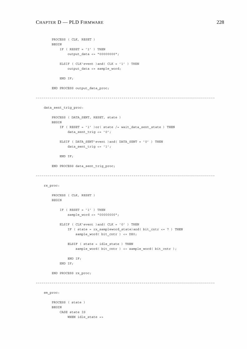
CHAPTER D — PLD FIRMWARE 228
PROCESS ( CLK, RESET )
BEGIN
IF ( RESET = ’1’ ) THEN
output_data <= "00000000";
ELSIF ( CLK’event )and( CLK = ’1’ ) THEN
output_data <= sample_word;
END IF;
END PROCESS output_data_proc;
------------------------------------------------------------------------------------------
data_sent_trig_proc:
PROCESS ( DATA_SENT, RESET, state )
BEGIN
IF ( RESET = ’1’ )or( state /= wait_data_sent_state ) THEN
data_sent_trig <= ’0’;
ELSIF ( DATA_SENT’event )and( DATA_SENT = ’0’ ) THEN
data_sent_trig <= ’1’;
END IF;
END PROCESS data_sent_trig_proc;
------------------------------------------------------------------------------------------
rx_proc:
PROCESS ( CLK, RESET )
BEGIN
IF ( RESET = ’1’ ) THEN
sample_word <= "00000000";
ELSIF ( CLK’event )and( CLK = ’0’ ) THEN
IF ( state = rx_sampleword_state)and( bit_cntr <= 7 ) THEN
sample_word( bit_cntr ) <= DX0;
ELSIF ( state = idle_state ) THEN
sample_word( bit_cntr ) <= sample_word( bit_cntr );
END IF;
END IF;
END PROCESS rx_proc;
------------------------------------------------------------------------------------------
sm_proc:
PROCESS ( state )
BEGIN
CASE state IS
WHEN idle_state =>

CHAPTER D — PLD FIRMWARE 229
next_state <= rx_sampleword_state;
WHEN rx_sampleword_state =>
next_state <= start_tx_state;
WHEN start_tx_state =>
next_state <= wait_data_sent_state;
WHEN wait_data_sent_state =>
next_state <= idle_state;
END CASE;
END PROCESS sm_proc;
------------------------------------------------------------------------------------------
sm_ctrl_proc:
PROCESS ( CLKX0, RESET )
BEGIN
IF ( RESET = ’1’ )or( data_sent_trig = ’1’ ) THEN
bit_cntr <= 0;
state <= idle_state;
ELSIF ( CLKX0’event )and( CLKX0 = ’1’ ) THEN
IF ( rx_start_trig = ’1’ )and( state = idle_state ) THEN
bit_cntr <= 0;
state <= next_state;
ELSIF ( state = rx_sampleword_state )and( bit_cntr < 7 ) THEN
bit_cntr <= bit_cntr+1;
state <= state;
ELSIF ( state = rx_sampleword_state )and( bit_cntr = 7 ) THEN
bit_cntr <= bit_cntr;
state <= next_state;
ELSIF ( state = start_tx_state ) THEN
bit_cntr <= bit_cntr;
state <= next_state;
ELSIF ( state = wait_data_sent_state )and( data_sent_trig = ’1’) THEN
bit_cntr <= bit_cntr;
state <= next_state;
ELSIF ( state = idle_state ) THEN
bit_cntr <= 0;
state <= state;
ELSE
bit_cntr <= bit_cntr;
state <= state;
END IF;
END IF;
END PROCESS sm_ctrl_proc;

CHAPTER D — PLD FIRMWARE 230
------------------------------------------------------------------------------------------
start_proc:
PROCESS ( FSX0, RESET )
BEGIN
IF ( RESET = ’1’ )or( state /= idle_state ) THEN
rx_start_trig <= ’0’;
ELSIF ( FSX0’event )and( FSX0 = ’1’ ) THEN
IF ( state = idle_state ) THEN
rx_start_trig <= ’1’;
END IF;
END IF;
END PROCESS start_proc;
------------------------------------------------------------------------------------------
tx_proc:
PROCESS ( CLK, RESET )
BEGIN
IF ( RESET = ’1’ ) THEN
signal_TX_DATA_RDY <= ’0’;
DATA_OUT <= "00000000";
ELSIF ( CLK’event )and( CLK = ’1’ ) THEN
IF ( state /= start_tx_state ) THEN
signal_TX_DATA_RDY <= ’0’;
DATA_OUT <= output_data;
ELSIF ( signal_TX_DATA_RDY = ’0’ ) THEN
signal_TX_DATA_RDY <= ’1’;
DATA_OUT <= output_data;
ELSE
signal_TX_DATA_RDY <= ’0’;
DATA_OUT <= output_data;
END IF;
END IF;
END PROCESS tx_proc;
END a;

CHAPTER D — PLD FIRMWARE 231
D.1.13 VHDL Code for the DSP SP RX Ctrl Module of FPGA Main-- PEC33 Main - RX interface between DSP serial port and UART 2002-11-07
-- Input Word Length: 8 Bits
-- Output Word Length: 32 Bits
LIBRARY ieee;
USE ieee.std_logic_1164.all;
USE ieee.std_logic_arith.all;
ENTITY DSP_SP_RX_Ctrl IS
PORT (
DATA_IN : IN STD_LOGIC_VECTOR( 7 DOWNTO 0 );
RX_DATA_RDY : IN STD_LOGIC;
DR0 : OUT STD_LOGIC;
FSR0 : OUT STD_LOGIC;
CLKR0 : OUT STD_LOGIC;
RESET : IN STD_LOGIC;
CLK : IN STD_LOGIC
);
END DSP_SP_RX_Ctrl;
ARCHITECTURE a OF DSP_SP_RX_Ctrl IS
TYPE rx_state_type IS ( idle_state, samplebyte_state, storeword_state );
TYPE tx_state_type IS ( idle_state, fs_state, tx_data_state );
SIGNAL rx_state : rx_state_type;
SIGNAL next_rx_state : rx_state_type;
SIGNAL tx_state : tx_state_type;
SIGNAL next_tx_state : tx_state_type;
SIGNAL rx_start_trig : STD_LOGIC;
SIGNAL tx_start_trig : STD_LOGIC;
SIGNAL rx_word_rdy : STD_LOGIC;
SIGNAL byte_cntr : INTEGER RANGE 0 TO 4;
SIGNAL bit_cntr : INTEGER RANGE 0 TO 32;
SIGNAL sample_word : STD_LOGIC_VECTOR ( 32 DOWNTO 0 );
SIGNAL slow_div_CLK : STD_LOGIC;
SIGNAL slow_CLK : STD_LOGIC;
BEGIN
CLKR0 <= slow_CLK;
------------------------------------------------------------------------------------------
rx_proc:
PROCESS ( CLK, RESET )
BEGIN
IF ( RESET = ’1’ ) THEN
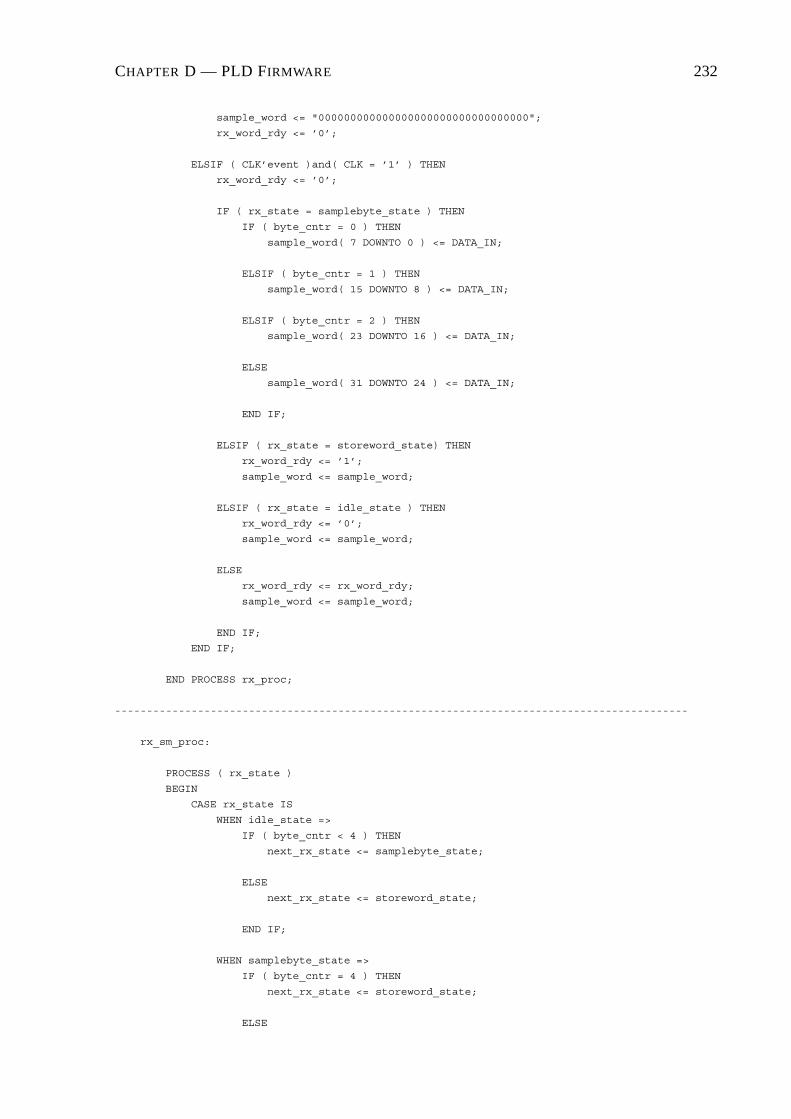
CHAPTER D — PLD FIRMWARE 232
sample_word <= "000000000000000000000000000000000";
rx_word_rdy <= ’0’;
ELSIF ( CLK’event )and( CLK = ’1’ ) THEN
rx_word_rdy <= ’0’;
IF ( rx_state = samplebyte_state ) THEN
IF ( byte_cntr = 0 ) THEN
sample_word( 7 DOWNTO 0 ) <= DATA_IN;
ELSIF ( byte_cntr = 1 ) THEN
sample_word( 15 DOWNTO 8 ) <= DATA_IN;
ELSIF ( byte_cntr = 2 ) THEN
sample_word( 23 DOWNTO 16 ) <= DATA_IN;
ELSE
sample_word( 31 DOWNTO 24 ) <= DATA_IN;
END IF;
ELSIF ( rx_state = storeword_state) THEN
rx_word_rdy <= ’1’;
sample_word <= sample_word;
ELSIF ( rx_state = idle_state ) THEN
rx_word_rdy <= ’0’;
sample_word <= sample_word;
ELSE
rx_word_rdy <= rx_word_rdy;
sample_word <= sample_word;
END IF;
END IF;
END PROCESS rx_proc;
------------------------------------------------------------------------------------------
rx_sm_proc:
PROCESS ( rx_state )
BEGIN
CASE rx_state IS
WHEN idle_state =>
IF ( byte_cntr < 4 ) THEN
next_rx_state <= samplebyte_state;
ELSE
next_rx_state <= storeword_state;
END IF;
WHEN samplebyte_state =>
IF ( byte_cntr = 4 ) THEN
next_rx_state <= storeword_state;
ELSE
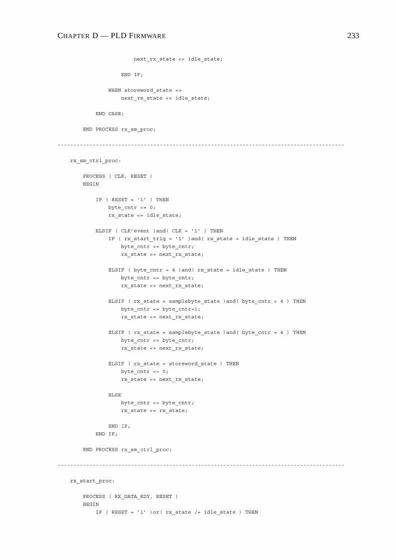
CHAPTER D — PLD FIRMWARE 233
next_rx_state <= idle_state;
END IF;
WHEN storeword_state =>
next_rx_state <= idle_state;
END CASE;
END PROCESS rx_sm_proc;
------------------------------------------------------------------------------------------
rx_sm_ctrl_proc:
PROCESS ( CLK, RESET )
BEGIN
IF ( RESET = ’1’ ) THEN
byte_cntr <= 0;
rx_state <= idle_state;
ELSIF ( CLK’event )and( CLK = ’1’ ) THEN
IF ( rx_start_trig = ’1’ )and( rx_state = idle_state ) THEN
byte_cntr <= byte_cntr;
rx_state <= next_rx_state;
ELSIF ( byte_cntr = 4 )and( rx_state = idle_state ) THEN
byte_cntr <= byte_cntr;
rx_state <= next_rx_state;
ELSIF ( rx_state = samplebyte_state )and( byte_cntr < 4 ) THEN
byte_cntr <= byte_cntr+1;
rx_state <= next_rx_state;
ELSIF ( rx_state = samplebyte_state )and( byte_cntr = 4 ) THEN
byte_cntr <= byte_cntr;
rx_state <= next_rx_state;
ELSIF ( rx_state = storeword_state ) THEN
byte_cntr <= 0;
rx_state <= next_rx_state;
ELSE
byte_cntr <= byte_cntr;
rx_state <= rx_state;
END IF;
END IF;
END PROCESS rx_sm_ctrl_proc;
------------------------------------------------------------------------------------------
rx_start_proc:
PROCESS ( RX_DATA_RDY, RESET )
BEGIN
IF ( RESET = ’1’ )or( rx_state /= idle_state ) THEN
CHAPTER D — PLD FIRMWARE 234
rx_start_trig <= ’0’;
ELSIF ( RX_DATA_RDY’event )and( RX_DATA_RDY = ’0’ ) THEN
IF ( rx_state = idle_state ) THEN
rx_start_trig <= ’1’;
ELSE
rx_start_trig <= ’0’;
END IF;
END IF;
END PROCESS rx_start_proc;
------------------------------------------------------------------------------------------
tx_proc:
PROCESS ( slow_CLK, RESET )
BEGIN
IF ( RESET = ’1’ ) THEN
FSR0 <= ’0’;
DR0 <= ’0’;
ELSIF ( slow_CLK’event )and( slow_CLK = ’1’ ) THEN
IF ( tx_state = fs_state ) THEN
FSR0 <= ’1’;
DR0 <= ’0’;
ELSIF ( tx_state = tx_data_state)and( bit_cntr < 32 ) THEN
FSR0 <= ’0’;
DR0 <= sample_word( bit_cntr );
ELSIF ( tx_state = tx_data_state)and( bit_cntr = 32 ) THEN
FSR0 <= ’0’;
DR0 <= ’0’;
ELSIF ( tx_state = idle_state ) THEN
FSR0 <= ’0’;
DR0 <= ’0’;
END IF;
END IF;
END PROCESS tx_proc;
------------------------------------------------------------------------------------------
tx_sm_proc:
PROCESS ( tx_state )
BEGIN
CASE tx_state IS
WHEN idle_state =>
next_tx_state <= fs_state;
WHEN fs_state =>
next_tx_state <= tx_data_state;

CHAPTER D — PLD FIRMWARE 235
WHEN tx_data_state =>
next_tx_state <= idle_state;
END CASE;
END PROCESS tx_sm_proc;
------------------------------------------------------------------------------------------
tx_sm_ctrl_proc:
PROCESS ( slow_CLK, RESET )
BEGIN
IF ( RESET = ’1’ ) THEN
bit_cntr <= 0;
tx_state <= idle_state;
ELSIF ( slow_CLK’event )and( slow_CLK = ’1’ ) THEN
IF ( tx_start_trig = ’1’ )and( tx_state = idle_state ) THEN
bit_cntr <= 0;
tx_state <= next_tx_state;
ELSIF ( tx_state = fs_state ) THEN
bit_cntr <= 0;
tx_state <= next_tx_state;
ELSIF ( tx_state = tx_data_state )and( bit_cntr < 32 ) THEN
bit_cntr <= bit_cntr+1;
tx_state <= tx_state;
ELSIF ( tx_state = tx_data_state )and( bit_cntr = 32 ) THEN
bit_cntr <= bit_cntr;
tx_state <= next_tx_state;
ELSIF ( tx_state = idle_state ) THEN
bit_cntr <= 0;
tx_state <= tx_state;
ELSE
bit_cntr <= bit_cntr;
tx_state <= tx_state;
END IF;
END IF;
END PROCESS tx_sm_ctrl_proc;
------------------------------------------------------------------------------------------
tx_start_proc:
PROCESS ( rx_word_rdy, RESET )
BEGIN
IF ( RESET = ’1’ )or( tx_state /= idle_state ) THEN
tx_start_trig <= ’0’;
ELSIF ( rx_word_rdy’event )and( rx_word_rdy = ’0’ ) THEN
IF ( tx_state = idle_state ) THEN
tx_start_trig <= ’1’;

CHAPTER D — PLD FIRMWARE 236
ELSE
tx_start_trig <= ’0’;
END IF;
END IF;
END PROCESS tx_start_proc;
------------------------------------------------------------------------------------------
slow_div_clk_proc:
PROCESS ( CLK, RESET )
BEGIN
IF ( RESET = ’1’ ) THEN
slow_div_CLK <= ’0’;
ELSIF ( CLK’event )and( CLK = ’0’ ) THEN
slow_div_CLK <= not slow_div_CLK;
END IF;
END PROCESS slow_div_clk_proc;
------------------------------------------------------------------------------------------
slow_clk_proc:
PROCESS ( slow_div_CLK, RESET )
BEGIN
IF ( RESET = ’1’ ) THEN
slow_CLK <= ’0’;
ELSIF ( slow_div_CLK’event )and( slow_div_CLK = ’1’ ) THEN
slow_CLK <= not slow_CLK;
END IF;
END PROCESS slow_clk_proc;
END a;

CHAPTER D — PLD FIRMWARE 237
D.1.14 VHDL Code for the Dev Sel Ctrl Module of FPGA Main-- PEC33 Main - Device Select Controller 2002-11-07
LIBRARY ieee;
USE ieee.std_logic_1164.all;
USE ieee.std_logic_arith.all;
-- ---------------------------------------
-- | Address | Device |
-- ------------------- |
-- | HEX | Binary | Selected |
-- ---------------------------------------
-- ---------------------------------------
-- | 0x4 | 0100 | Flash RAM 0 |
-- ---------------------------------------
-- | 0x5 | 0101 | FPGA Main |
-- ---------------------------------------
-- | 0x6 | 0110 | FPGA Analog |
-- ---------------------------------------
-- | 0xA | 1010 | Expansion bus 0 |
-- ---------------------------------------
-- | 0xB | 1011 | Expansion bus 1 |
-- ---------------------------------------
-- | 0xC | 1100 | Flash RAM 1 |
-- ---------------------------------------
ENTITY DEV_SEL_Ctrl IS
PORT(
FPGAMAIN_nCS : OUT STD_LOGIC;
FPGANLG_nCS : OUT STD_LOGIC;
FRAM0_nCS : OUT STD_LOGIC;
FRAM1_nCS : OUT STD_LOGIC;
EXBUS0_nCS : OUT STD_LOGIC;
EXBUS1_nCS : OUT STD_LOGIC;
ADDR : IN STD_LOGIC_VECTOR( 3 DOWNTO 0 );
RESET : IN STD_LOGIC;
CLK : IN STD_LOGIC
);
END DEV_SEL_Ctrl;
ARCHITECTURE a OF DEV_SEL_Ctrl IS
BEGIN
sel_dev_proc:
PROCESS ( CLK, RESET )
BEGIN
IF ( RESET = ’1’ ) THEN
FPGAMAIN_nCS <= ’1’;
FPGANLG_nCS <= ’1’;
FRAM0_nCS <= ’1’;
FRAM1_nCS <= ’1’;
EXBUS0_nCS <= ’1’;

CHAPTER D — PLD FIRMWARE 238
EXBUS1_nCS <= ’1’;
ELSIF ( CLK’event )and( CLK = ’1’ ) THEN
IF ( ADDR = "0100" ) THEN
FPGAMAIN_nCS <= ’1’;
FPGANLG_nCS <= ’1’;
FRAM0_nCS <= ’0’;
FRAM1_nCS <= ’1’;
EXBUS0_nCS <= ’1’;
EXBUS1_nCS <= ’1’;
ELSIF ( ADDR = "0101" ) THEN
FPGAMAIN_nCS <= ’0’;
FPGANLG_nCS <= ’1’;
FRAM0_nCS <= ’1’;
FRAM1_nCS <= ’1’;
EXBUS0_nCS <= ’1’;
EXBUS1_nCS <= ’1’;
ELSIF ( ADDR = "0110" ) THEN
FPGAMAIN_nCS <= ’1’;
FPGANLG_nCS <= ’0’;
FRAM0_nCS <= ’1’;
FRAM1_nCS <= ’1’;
EXBUS0_nCS <= ’1’;
EXBUS1_nCS <= ’1’;
ELSIF ( ADDR = "1010" ) THEN
FPGAMAIN_nCS <= ’1’;
FPGANLG_nCS <= ’1’;
FRAM0_nCS <= ’1’;
FRAM1_nCS <= ’1’;
EXBUS0_nCS <= ’0’;
EXBUS1_nCS <= ’1’;
ELSIF ( ADDR = "1011" ) THEN
FPGAMAIN_nCS <= ’1’;
FPGANLG_nCS <= ’1’;
FRAM0_nCS <= ’1’;
FRAM1_nCS <= ’1’;
EXBUS0_nCS <= ’1’;
EXBUS1_nCS <= ’0’;
ELSIF ( ADDR = "1100" ) THEN
FPGAMAIN_nCS <= ’1’;
FPGANLG_nCS <= ’1’;
FRAM0_nCS <= ’1’;
FRAM1_nCS <= ’0’;
EXBUS0_nCS <= ’1’;
EXBUS1_nCS <= ’1’;
ELSE
FPGAMAIN_nCS <= ’1’;
FPGANLG_nCS <= ’1’;
FRAM0_nCS <= ’1’;
FRAM1_nCS <= ’1’;
EXBUS0_nCS <= ’1’;
EXBUS1_nCS <= ’1’;

CHAPTER D — PLD FIRMWARE 239
END IF;
END IF;
END PROCESS sel_dev_proc;
END a;
CHAPTER D — PLD FIRMWARE 240
D.1.15 VHDL Code for the DSP Boot Ctrl Module of FPGA Main-- PEC33 Main - Reset & boot controller 2002-11-07
LIBRARY ieee;
USE ieee.std_logic_1164.all;
USE ieee.std_logic_arith.all;
-- The BOOT_TYPE input is from the DIP switch 1
-- -------------------------
-- | Value of | Boot data |
-- | BOOT_TYPE | source |
-- -------------------------
-- -------------------------
-- | 0 | Serial port |
-- -------------------------
-- | 1 | Flash RAM 0 |
-- -------------------------
ENTITY DSP_BOOT_Ctrl IS
PORT(
BOOT_TYPE : IN STD_LOGIC;
nINT1 : OUT STD_LOGIC;
nINT3 : OUT STD_LOGIC;
DSP_nRESET : OUT STD_LOGIC;
RESET : IN STD_LOGIC;
CLK : IN STD_LOGIC
);
END DSP_BOOT_Ctrl;
ARCHITECTURE a OF DSP_BOOT_Ctrl IS
TYPE state_type IS ( state0, state1, state2, state3, state4 );
SIGNAL signal_BOOT_TYPE : STD_LOGIC;
SIGNAL signal_DSP_nRESET : STD_LOGIC;
SIGNAL reset_trig : STD_LOGIC;
SIGNAL reset_cntr : INTEGER RANGE 0 TO 63;
SIGNAL int_cntr : INTEGER RANGE 0 TO 15;
SIGNAL dsp_resetting : STD_LOGIC;
SIGNAL state : state_type;
BEGIN
DSP_nRESET <= ’0’ WHEN ( state = state2 ) ELSE ’1’;
nINT1 <= ’0’ WHEN ( state = state4 )and( signal_BOOT_TYPE = ’0’ ) ELSE ’1’;
nINT3 <= ’0’ WHEN ( state = state4 )and( signal_BOOT_TYPE = ’1’ ) ELSE ’1’;
------------------------------------------------------------------------------------------
boot_type_proc:
PROCESS ( CLK )
BEGIN

CHAPTER D — PLD FIRMWARE 241
IF ( CLK’event )and( CLK = ’1’ ) THEN
signal_BOOT_TYPE <= BOOT_TYPE;
END IF;
END PROCESS boot_type_proc;
------------------------------------------------------------------------------------------
rst_dsp_trig_proc:
PROCESS ( RESET )
BEGIN
IF ( state = state1 ) THEN
reset_trig <= ’0’;
ELSIF ( RESET’event )and( RESET = ’0’ ) THEN
reset_trig <= ’1’;
END IF;
END PROCESS rst_dsp_trig_proc;
------------------------------------------------------------------------------------------
sm_ctrl_proc:
PROCESS ( CLK, RESET )
BEGIN
IF ( RESET = ’1’ ) THEN
state <= state0;
reset_cntr <= 0;
int_cntr <= 0;
ELSIF ( CLK’event )and( CLK = ’1’ ) THEN
IF ( reset_trig = ’1’ )and( state = state0 ) THEN
state <= state1;
reset_cntr <= 0;
int_cntr <= 0;
ELSIF ( state = state1 )and( reset_cntr < 10 ) THEN
state <= state;
reset_cntr <= reset_cntr+1;
int_cntr <= 0;
ELSIF ( state = state1 )and( reset_cntr = 10 ) THEN
state <= state2;
reset_cntr <= reset_cntr+1;
int_cntr <= int_cntr;
ELSIF ( state = state2 )and( reset_cntr < 60 ) THEN
state <= state;
reset_cntr <= reset_cntr+1;
int_cntr <= 0;
ELSIF ( state = state2 )and( reset_cntr = 60 ) THEN
state <= state3;
reset_cntr <= reset_cntr;
int_cntr <= int_cntr;
CHAPTER D — PLD FIRMWARE 242
ELSIF ( state = state3 )and( int_cntr < 7 ) THEN
state <= state;
reset_cntr <= 0;
int_cntr <= int_cntr+1;
ELSIF ( state = state3 )and( int_cntr = 7 ) THEN
state <= state4;
reset_cntr <= 0;
int_cntr <= int_cntr+1;
ELSIF ( state = state4 )and( int_cntr < 8 ) THEN
state <= state;
reset_cntr <= 0;
int_cntr <= int_cntr+1;
ELSIF ( state = state4 )and( int_cntr = 8 ) THEN
state <= state0;
reset_cntr <= 0;
int_cntr <= int_cntr;
ELSE
state <= state;
reset_cntr <= reset_cntr;
int_cntr <= int_cntr;
END IF;
END IF;
END PROCESS sm_ctrl_proc;
END a;

CHAPTER D — PLD FIRMWARE 243
D.1.16 VHDL Code for the Clk Gen Ctrl Module of FPGA Main-- PEC33 Main - Clock Generator 2002-11-07
LIBRARY ieee;
USE ieee.std_logic_1164.all;
USE ieee.std_logic_arith.all;
ENTITY CLK_GEN_Ctrl IS
PORT(
FPGANLG_CLK : OUT STD_LOGIC; -- 30MHz
DSP_CLK : OUT STD_LOGIC; -- 15MHz
EXBUS_CLK : OUT STD_LOGIC; -- 30MHz
RESET : IN STD_LOGIC;
CLK : IN STD_LOGIC
);
END CLK_GEN_Ctrl;
ARCHITECTURE a OF CLK_GEN_Ctrl IS
SIGNAL signal_dsp_clk : STD_LOGIC;
BEGIN
FPGANLG_CLK <= CLK;
DSP_CLK <= signal_dsp_clk;
EXBUS_CLK <= CLK;
------------------------------------------------------------------------------------------
dsp_clk_gen_proc:
PROCESS ( CLK, RESET )
BEGIN
IF ( CLK’event )and( CLK = ’1’ ) THEN
signal_dsp_clk <= not signal_dsp_clk;
END IF;
END PROCESS dsp_clk_gen_proc;
END a;
CHAPTER D — PLD FIRMWARE 244
D.2 Firmware for FPGA Analog

CHAPTER D — PLD FIRMWARE 245
D.2.1 Graphical Design File for FPGA Analog
ADC3_SAMP_CHAN7[2..0]ADC3_SAMP_CHAN6[2..0]
GLOBAL_RESET
ADC3_SAMP_CHAN5[2..0]ADC3_SAMP_CHAN4[2..0]ADC3_SAMP_CHAN3[2..0]ADC3_SAMP_CHAN2[2..0]
ADC3_CHAN[2..0]
ADC3_SAMP_CHAN1[2..0]ADC3_SAMP_CHAN0[2..0]ADC3_DATA_RDY
ADC3_DATA_VALIDGLOBAL_RESET
ADC3_DATA_RDYADC3_CHAN[2..0]ADC3_DATA_IN[9..0]
ADC3_DATA[12..0]
GLOBAL_CLKGLOBAL_RESET
ADC3_DATA_VALIDADC3_DATA_RDY
ADC_STATUS_IN3
ADC3_nENADC3_CHAN[2..0]ADC3_CONF_DATA[9..0]
ADC3_DATA_IN[9..0]
GLOBAL_RESET
ADC2_SAMP_CHAN5[2..0]ADC2_SAMP_CHAN6[2..0]ADC2_SAMP_CHAN7[2..0]
ADC2_SAMP_CHAN1[2..0]ADC2_SAMP_CHAN2[2..0]
ADC2_SAMP_CHAN4[2..0]ADC2_SAMP_CHAN3[2..0] ADC2_CHAN[2..0]
ADC2_SAMP_CHAN0[2..0]ADC2_DATA_RDY
ADC2_DATA_VALIDGLOBAL_RESET
ADC2_DATA[12..0]
ADC2_DATA_IN[9..0]ADC2_CHAN[2..0]ADC2_DATA_RDY
GLOBAL_RESETGLOBAL_CLK
ADC2_DATA_RDYADC2_DATA_VALID
ADC2_DATA_IN[9..0]
ADC_STATUS_IN2
ADC2_CONF_DATA[9..0]ADC2_CHAN[2..0]ADC2_nEN
GLOBAL_RESETADC1_SAMP_CHAN7[2..0]ADC1_SAMP_CHAN6[2..0]ADC1_SAMP_CHAN5[2..0]ADC1_SAMP_CHAN4[2..0]ADC1_SAMP_CHAN3[2..0]ADC1_SAMP_CHAN2[2..0]ADC1_SAMP_CHAN1[2..0]
ADC1_CHAN[2..0]
ADC1_SAMP_CHAN0[2..0]ADC1_DATA_RDY
ADC1_DATA_VALIDGLOBAL_RESET
ADC1_DATA_RDY ADC1_DATA[12..0]ADC1_CHAN[2..0]ADC1_DATA_IN[9..0]
GLOBAL_CLKGLOBAL_RESETADC1_nEN
ADC1_DATA_VALIDADC1_DATA_RDYADC1_DATA_IN[9..0]
ADC_STATUS_IN1
ADC1_CHAN[2..0]ADC1_CONF_DATA[9..0]
ADC0_SAMP_CHAN4[2..0]ADC0_SAMP_CHAN5[2..0]
GLOBAL_RESETADC0_SAMP_CHAN7[2..0]ADC0_SAMP_CHAN6[2..0]
ADC0_SAMP_CHAN0[2..0]ADC0_SAMP_CHAN1[2..0]
ADC0_SAMP_CHAN3[2..0]ADC0_SAMP_CHAN2[2..0]
ADC0_CHAN[2..0]
ADC0_DATA_RDY
ADC0_DATA_VALIDGLOBAL_RESET
ADC0_DATA_RDYADC0_CHAN[2..0]
ADC0_DATA[12..0]
ADC0_DATA_IN[9..0]
ADC0_CHAN[2..0]ADC0_nENGLOBAL_RESETGLOBAL_CLK ADC0_DATA_VALID
ADC0_DATA_RDYADC0_DATA_IN[9..0]
ADC_STATUS_IN0
ADC0_CONF_DATA[9..0]
AND2
pec33_analog_ver4@184ADC3_SDOUT INPUT
pec33_analog_ver4@190ADC3_SCLKOUTPUTpec33_analog_ver4@187ADC3_nCSOUTPUTpec33_analog_ver4@189ADC3_SDINOUTPUT
AND2
pec33_analog_ver4@182ADC2_SDOUT INPUT pec33_analog_ver4@176ADC2_SDINOUTPUT
pec33_analog_ver4@179ADC2_nCSOUTPUT
pec33_analog_ver4@177ADC2_SCLKOUTPUT
AND2
pec33_analog_ver4@174ADC1_SDOUT INPUT
pec33_analog_ver4@175ADC1_nCSOUTPUTpec33_analog_ver4@172ADC1_SDINOUTPUT
pec33_analog_ver4@173ADC1_SCLKOUTPUT
pec33_analog_ver4@168ADC0_SCLKOUTPUT
AND2
pec33_analog_ver4@169ADC0_SDOUT INPUT
pec33_analog_ver4@170ADC0_nCSOUTPUTpec33_analog_ver4@167ADC0_SDINOUTPUT
Figure D.5: Graphical Design File of FPGA Analog (Part 1 of 5)

CHAPTER D — PLD FIRMWARE 246
GLOBAL_RESETGLOBAL_CLK
KP_ROW[3..0] KP_COL[2..0]KEYVAL[3..0]
GLOBAL_RESETINT_EN[14..0]PWM1_COUNTERZERO
GLOBAL_CLK
PWM1_COMPDOWNPWM1_COMPUPPWM0_COUNTERZERO
PWM1_RAMPDIR
PWM_ERR_BOT_OUT[8..0]PWM_STATUS_OUT[7..0]INT_REG[5..0]
PWM_ERR_TOP[8..0]PWM_ERR_BOT[8..0]PWM0_COMPUPPWM0_COMPDOWNPWM0_RAMPDIR
KEYVAL_OUT[3..0]ADC_STATUS_OUT[3..0]
PWM_ERR_TOP_OUT[8..0]
ADC_STATUS_IN[3..0]KEYVAL[3..0]
GLOBAL_CLKGLOBAL_RESET
DAC3_B_DATA[11..0]DAC3_CTRL_DATA[1..0]DAC3_nLOAD
DAC3_B_CONF_DATA[2..0]DAC3_A_DATA[11..0]DAC3_A_CONF_DATA[2..0]
GLOBAL_RESETGLOBAL_CLK
DAC2_nLOADDAC2_CTRL_DATA[1..0]
DAC2_B_CONF_DATA[2..0]DAC2_B_DATA[11..0]
DAC2_A_DATA[11..0]DAC2_A_CONF_DATA[2..0]
GLOBAL_CLK
DAC1_CTRL_DATA[1..0]DAC1_nLOADGLOBAL_RESET
DAC1_B_DATA[11..0]DAC1_B_CONF_DATA[2..0]
DAC1_A_CONF_DATA[2..0]DAC1_A_DATA[11..0]
GLOBAL_CLKGLOBAL_RESETDAC0_nLOAD
DAC0_B_DATA[11..0]DAC0_CTRL_DATA[1..0]
DAC0_B_CONF_DATA[2..0]DAC0_A_DATA[11..0]DAC0_A_CONF_DATA[2..0]
pec33_analog_ver4@142KP_COL2OUTPUT
pec33_analog_ver4@140 KP_ROW1 INPUT
pec33_analog_ver4@139 KP_ROW2 INPUT
pec33_analog_ver4@136 KP_ROW3 INPUT pec33_analog_ver4@144KP_COL0OUTPUT
pec33_analog_ver4@143KP_COL1OUTPUT
pec33_analog_ver4@141 KP_ROW0 INPUT
pec33_analog_ver4@83DSP_nINT2OUTPUTpec33_analog_ver4@85DSP_nINT0OUTPUT
pec33_analog_ver4@206DAC3_nSYNCOUTPUT
pec33_analog_ver4@207DAC3_SCLKOUTPUT
pec33_analog_ver4@205DAC3_nLDACOUTPUT
pec33_analog_ver4@208DAC3_SDINOUTPUT
pec33_analog_ver4@204DAC2_SDINOUTPUT
pec33_analog_ver4@202DAC2_nSYNCOUTPUT
pec33_analog_ver4@200DAC2_nLDACOUTPUTpec33_analog_ver4@203DAC2_SCLKOUTPUT
pec33_analog_ver4@198DAC1_SCLKOUTPUT
pec33_analog_ver4@196DAC1_nLDACOUTPUT
pec33_analog_ver4@197DAC1_nSYNCOUTPUTpec33_analog_ver4@199DAC1_SDINOUTPUT
pec33_analog_ver4@192DAC0_nSYNCOUTPUT
pec33_analog_ver4@193DAC0_SCLKOUTPUT
pec33_analog_ver4@191DAC0_nLDACOUTPUT
pec33_analog_ver4@195DAC0_SDINOUTPUT
Figure D.6: Graphical Design File of FPGA Analog (Part 2 of 5)

CHAPTER D — PLD FIRMWARE 247
CMD_REG1_EN
INT_REG_EN
CMD_REG0_ENINT_EN_EN
PWM_ERR_BOT_EN
PWM1_DOWNVAL_ENPWM_ERR_TOP_EN
PWM1_UPVAL_ENPWM1_DEADTIME_EN
PWM1_REFC_EN
PWM1_TRIFREQSCALE_ENPWM1_TRIMAX_ENPWM1_REFN_EN
PWM1_REFB_EN
PWM0_UPVAL_ENPWM0_DOWNVAL_ENPWM1_REFA_EN
PWM0_REFN_ENPWM0_TRIMAX_ENPWM0_TRIFREQSCALE_ENPWM0_DEADTIME_EN
PWM_STATUS_ENPWM0_REFA_ENPWM0_REFB_ENPWM0_REFC_EN
LCD_CHAR_ENLCD_ADDR_ENLCD_STATUS_ENKEYVAL_EN
ADC3_SAMP_CHAN5_ENADC3_SAMP_CHAN6_ENADC3_SAMP_CHAN7_ENLCD_MODE_EN
ADC3_SAMP_CHAN1_ENADC3_SAMP_CHAN2_ENADC3_SAMP_CHAN3_ENADC3_SAMP_CHAN4_EN
ADC2_SAMP_CHAN7_ENADC3_CONF_ENADC3_DATA_ENADC3_SAMP_CHAN0_EN
DSP_H3
GLOBAL_RESET ADC2_SAMP_CHAN3_ENADC2_SAMP_CHAN4_ENADC2_SAMP_CHAN5_ENADC2_SAMP_CHAN6_EN
ADDR[9..0] ADC2_SAMP_CHAN0_ENADC2_DATA_EN
ADC2_SAMP_CHAN1_ENADC2_SAMP_CHAN2_EN
ADC2_CONF_EN
ADC1_SAMP_CHAN5_ENADC1_SAMP_CHAN6_ENADC1_SAMP_CHAN7_EN
ADC1_SAMP_CHAN3_EN
ADC1_SAMP_CHAN1_ENADC1_SAMP_CHAN2_EN
ADC1_SAMP_CHAN4_EN
ADC0_SAMP_CHAN7_ENADC1_CONF_ENADC1_DATA_ENADC1_SAMP_CHAN0_EN
ADC0_SAMP_CHAN3_ENADC0_SAMP_CHAN4_ENADC0_SAMP_CHAN5_ENADC0_SAMP_CHAN6_EN
ADC0_SAMP_CHAN0_ENADC0_DATA_EN
ADC0_SAMP_CHAN1_ENADC0_SAMP_CHAN2_EN
ADC0_CONF_EN
DAC3_B_CONF_ENDAC3_B_DATA_ENADC_STATUS_EN
DAC2_B_DATA_ENDAC3_CTRL_ENDAC3_A_CONF_ENDAC3_A_DATA_EN
DAC2_A_CONF_EN
DAC2_B_CONF_EN
DAC2_CTRL_EN
DAC2_A_DATA_EN
DAC1_A_CONF_EN
DAC1_B_CONF_ENDAC1_A_DATA_EN
DAC1_B_DATA_EN
DAC0_A_DATA_ENDAC0_B_CONF_ENDAC0_B_DATA_ENDAC1_CTRL_EN
DAC0_A_CONF_ENDAC0_CTRL_EN
LCD_RESET
PWM1_nENPWM0_nEN
CMD_REG1[5..0]GLOBAL_RESETGLOBAL_CLK
ADC2_nENADC3_nEN
LCD_UPDATE_DATALCD_UPDATE_MODE
CMD_REG0[6..0] ADC0_nEN
DAC2_nLOAD
ADC1_nEN
DAC3_nLOAD
DAC1_nLOADDAC0_nLOAD
pec33_analog_ver4@79 GLOBAL_CLK INPUT
pec33_analog_ver4@78 DSP_nSTRB INPUT
pec33_analog_ver4@75FPGA_nRESET INPUTNOT
pec33_analog_ver4@92 ADDR8 INPUT
pec33_analog_ver4@90 ADDR9 INPUT
pec33_analog_ver4@74 FPGA_nCS INPUT
pec33_analog_ver4@96 ADDR4 INPUT
pec33_analog_ver4@95 ADDR5 INPUT
pec33_analog_ver4@94 ADDR6 INPUT
pec33_analog_ver4@93 ADDR7 INPUT
pec33_analog_ver4@101 ADDR0 INPUT
pec33_analog_ver4@100 ADDR1 INPUT
pec33_analog_ver4@99 ADDR2 INPUT
pec33_analog_ver4@97 ADDR3 INPUT
Figure D.7: Graphical Design File of FPGA Analog (Part 3 of 5)

CHAPTER D — PLD FIRMWARE 248
DSP_H3GLOBAL_RESETCMD_REG1_ENCMD_REG0_EN
INT_EN_ENPWM_ERR_BOT_EN
INT_REG_EN
PWM_ERR_TOP_ENPWM1_DOWNVAL_ENPWM1_UPVAL_ENPWM1_DEADTIME_ENPWM1_TRIFREQSCALE_ENPWM1_TRIMAX_ENPWM1_REFN_ENPWM1_REFC_ENPWM1_REFB_ENPWM1_REFA_ENPWM0_DOWNVAL_ENPWM0_UPVAL_EN
DATA[15..0]RnWCMD_REG1[5..0]CMD_REG0[6..0]PWM0_DEADTIME_EN
PWM0_TRIFREQSCALE_ENPWM0_TRIMAX_ENPWM0_REFN_EN
INT_EN[14..0]PWM1_COMPDOWNVAL[9..0]PWM1_COMPUPVAL[9..0]PWM1_DEADTIME[9..0]PWM0_REFC_EN
PWM0_REFB_ENPWM0_REFA_ENPWM_STATUS_EN
PWM1_TRIFREQSCALE[9..0]PWM1_TRIMAX[9..0]PWM1_REFN[9..0]PWM1_REFC[9..0]KEYVAL_EN
LCD_STATUS_ENLCD_ADDR_ENLCD_CHAR_EN
PWM1_REFB[9..0]PWM1_REFA[9..0]PWM0_COMPDOWNVAL[9..0]PWM0_COMPUPVAL[9..0]LCD_MODE_EN
ADC3_SAMP_CHAN7_ENADC3_SAMP_CHAN6_ENADC3_SAMP_CHAN5_EN
PWM0_DEADTIME[9..0]PWM0_TRIFREQSCALE[9..0]PWM0_TRIMAX[9..0]PWM0_REFN[9..0]ADC3_SAMP_CHAN4_EN
ADC3_SAMP_CHAN3_ENADC3_SAMP_CHAN2_ENADC3_SAMP_CHAN1_EN
PWM0_REFC[9..0]PWM0_REFB[9..0]PWM0_REFA[9..0]LCD_ADDR[6..0]ADC3_SAMP_CHAN0_EN
ADC3_DATA_ENADC3_CONF_ENADC2_SAMP_CHAN7_EN
LCD_CHAR[7..0]LCD_MODE_DATA[7..0]ADC3_SAMP_CHAN7[2..0]ADC3_SAMP_CHAN6[2..0]ADC2_SAMP_CHAN6_EN
ADC2_SAMP_CHAN5_ENADC2_SAMP_CHAN4_ENADC2_SAMP_CHAN3_EN
ADC3_SAMP_CHAN5[2..0]ADC3_SAMP_CHAN4[2..0]ADC3_SAMP_CHAN3[2..0]ADC3_SAMP_CHAN2[2..0]ADC2_SAMP_CHAN2_EN
ADC2_SAMP_CHAN1_ENADC2_SAMP_CHAN0_ENADC2_DATA_EN
ADC3_SAMP_CHAN1[2..0]ADC3_SAMP_CHAN0[2..0]ADC3_CONF_DATA[9..0]ADC2_SAMP_CHAN7[2..0]ADC2_CONF_EN
ADC1_SAMP_CHAN7_ENADC1_SAMP_CHAN6_ENADC1_SAMP_CHAN5_EN
ADC2_SAMP_CHAN6[2..0]ADC2_SAMP_CHAN5[2..0]ADC2_SAMP_CHAN4[2..0]ADC2_SAMP_CHAN3[2..0]ADC1_SAMP_CHAN4_EN
ADC1_SAMP_CHAN3_ENADC1_SAMP_CHAN2_ENADC1_SAMP_CHAN1_EN
ADC2_SAMP_CHAN2[2..0]ADC2_SAMP_CHAN1[2..0]ADC2_SAMP_CHAN0[2..0]ADC2_CONF_DATA[9..0]ADC1_SAMP_CHAN0_EN
ADC1_DATA_ENADC1_CONF_ENADC0_SAMP_CHAN7_EN
ADC1_SAMP_CHAN7[2..0]ADC1_SAMP_CHAN6[2..0]ADC1_SAMP_CHAN5[2..0]ADC1_SAMP_CHAN4[2..0]ADC0_SAMP_CHAN6_EN
ADC0_SAMP_CHAN5_ENADC0_SAMP_CHAN4_ENADC0_SAMP_CHAN3_EN
ADC1_SAMP_CHAN3[2..0]ADC1_SAMP_CHAN2[2..0]ADC1_SAMP_CHAN1[2..0]ADC1_SAMP_CHAN0[2..0]ADC0_SAMP_CHAN2_EN
ADC0_SAMP_CHAN1_ENADC0_SAMP_CHAN0_EN
ADC0_DATA_EN
ADC1_CONF_DATA[9..0]ADC0_SAMP_CHAN7[2..0]ADC0_SAMP_CHAN6[2..0]ADC0_SAMP_CHAN5[2..0]ADC0_CONF_EN
ADC_STATUS_ENDAC3_B_DATA_ENDAC3_B_CONF_EN
ADC0_SAMP_CHAN4[2..0]ADC0_SAMP_CHAN3[2..0]ADC0_SAMP_CHAN2[2..0]ADC0_SAMP_CHAN1[2..0]DAC3_A_DATA_EN
DAC3_A_CONF_ENDAC3_CTRL_ENDAC2_B_DATA_EN
ADC0_SAMP_CHAN0[2..0]ADC0_CONF_DATA[9..0]DAC3_B_CONF_DATA[2..0]DAC3_B_DATA[11..0]DAC2_B_CONF_EN
DAC2_A_DATA_ENDAC2_A_CONF_ENDAC2_CTRL_EN
DAC3_A_CONF_DATA[2..0]DAC3_A_DATA[11..0]DAC3_CTRL_DATA[1..0]DAC2_B_CONF_DATA[2..0]DAC1_B_DATA_EN
DAC1_B_CONF_ENDAC1_A_DATA_ENDAC1_A_CONF_EN
DAC2_B_DATA[11..0]DAC2_A_CONF_DATA[2..0]DAC2_A_DATA[11..0]DAC2_CTRL_DATA[1..0]DAC1_CTRL_EN
DAC0_B_DATA_ENDAC0_B_CONF_ENDAC0_A_DATA_EN
DAC1_B_CONF_DATA[2..0]DAC1_B_DATA[11..0]DAC1_A_CONF_DATA[2..0]DAC1_A_DATA[11..0]DAC0_A_CONF_EN
DAC0_CTRL_EN
PWM_ERR_BOT_OUT[8..0]PWM_ERR_TOP_OUT[8..0]
INT_REG[5..0]DAC1_CTRL_DATA[1..0]DAC0_B_CONF_DATA[2..0]DAC0_B_DATA[11..0]DAC0_A_CONF_DATA[2..0]
PWM_STATUS_OUT7PWM_STATUS_OUT6PWM_STATUS_OUT5
DAC0_A_DATA[11..0]DAC0_CTRL_DATA[1..0]
PWM_STATUS_OUT4PWM_STATUS_OUT3PWM_STATUS_OUT2PWM_STATUS_OUT1
KEYVAL_OUT[3..0]PWM_STATUS_OUT0
LCD_RDYnBSYADC_STATUS_OUT3ADC3_DATA[12..0]ADC_STATUS_OUT2ADC2_DATA[12..0]ADC_STATUS_OUT1ADC1_DATA[12..0]ADC_STATUS_OUT0ADC0_DATA[12..0]
pec33_analog_ver4@37DATA12BIDIR
pec33_analog_ver4@36DATA13BIDIR
pec33_analog_ver4@31DATA14BIDIR
pec33_analog_ver4@30DATA15BIDIR
pec33_analog_ver4@41DATA8BIDIR
pec33_analog_ver4@40DATA9BIDIR
pec33_analog_ver4@39DATA10BIDIR
pec33_analog_ver4@38DATA11BIDIR
pec33_analog_ver4@47DATA4BIDIR
pec33_analog_ver4@46DATA5BIDIR
pec33_analog_ver4@45DATA6BIDIR
pec33_analog_ver4@44DATA7BIDIR
pec33_analog_ver4@86DATA0BIDIR
pec33_analog_ver4@87DATA1BIDIR
pec33_analog_ver4@88DATA2BIDIR
pec33_analog_ver4@89DATA3BIDIR
Figure D.8: Graphical Design File of FPGA Analog (Part 4 of 5)

CHAPTER D — PLD FIRMWARE 249
PWM0_COUNTERZERO
DAC0_nLDAC
GLOBAL_CLKGLOBAL_RESET
INT_EN0
INT_REG4
INT_REG0
DSP_nINT0
PWM0_COMPDOWN
GLOBAL_CLKGLOBAL_RESETPWM1_nENPWM1_COMPDOWNVAL[9..0]PWM1_COMPUPVAL[9..0]PWM1_REFN[9..0]
PWM1_COUNTERZEROPWM1_RAMPDIR
PWM1_REFC[9..0]PWM1_REFB[9..0]PWM1_REFA[9..0]PWM1_DEADTIME[9..0]
PWM1_COMPDOWNPWM1_COMPUP
PWM1_TRIFREQSCALE[9..0]PWM1_TRIMAX[9..0]
GLOBAL_CLKGLOBAL_RESETPWM0_nENPWM0_COMPDOWNVAL[9..0]PWM0_COMPUPVAL[9..0]PWM0_REFN[9..0]PWM0_REFC[9..0]
PWM0_COUNTERZEROPWM0_RAMPDIR
PWM0_REFB[9..0]PWM0_REFA[9..0]PWM0_DEADTIME[9..0]PWM0_TRIFREQSCALE[9..0]
PWM0_COMPDOWNPWM0_COMPUP
PWM0_TRIMAX[9..0]
GLOBAL_CLKGLOBAL_RESETLCD_RESETLCD_UPDATE_DATALCD_ADDR[6..0]LCD_CHAR[7..0]
LCD_RDYnBSY
LCD_UPDATE_MODELCD_MODE_DATA[7..0]
LCD_DATA[7..0]
GND pec33_analog_ver4@183DSP_H3INPUT
NOTpec33_analog_ver4@61LED7OUTPUT
pec33_analog_ver4@80DSP_RnWINPUT
NOTpec33_analog_ver4@60LED6OUTPUT
NOT
NOTpec33_analog_ver4@57LED4OUTPUT
pec33_analog_ver4@58LED5OUTPUT
NOT
NOT
pec33_analog_ver4@56LED3OUTPUT
NOT
pec33_analog_ver4@55LED2OUTPUT
pec33_analog_ver4@54LED1OUTPUT
NOTpec33_analog_ver4@53LED0OUTPUT
pec33_analog_ver4@16 PWM_ERR_BOT8 INPUTpec33_analog_ver4@15 PWM_ERR_TOP8 INPUT
pec33_analog_ver4@125PWM_DC_BOTOUTPUTpec33_analog_ver4@122PWM_DC_TOPOUTPUT
VCC
pec33_analog_ver4@113PWM1_N_BOTOUTPUT
pec33_analog_ver4@115PWM1_C_BOTOUTPUT
pec33_analog_ver4@112PWM1_N_TOPOUTPUT
pec33_analog_ver4@28 PWM_ERR_TOP7 INPUT
pec33_analog_ver4@29 PWM_ERR_BOT7 INPUT pec33_analog_ver4@119PWM1_B_BOTOUTPUT
pec33_analog_ver4@114PWM1_C_TOPOUTPUT
pec33_analog_ver4@24 PWM_ERR_TOP5 INPUT
pec33_analog_ver4@25 PWM_ERR_BOT5 INPUT
pec33_analog_ver4@27 PWM_ERR_BOT6 INPUTpec33_analog_ver4@26 PWM_ERR_TOP6 INPUT
pec33_analog_ver4@121PWM1_A_BOTOUTPUT
pec33_analog_ver4@116PWM1_B_TOPOUTPUT
pec33_analog_ver4@18 PWM_ERR_BOT4 INPUTpec33_analog_ver4@17 PWM_ERR_TOP4 INPUT
pec33_analog_ver4@120PWM1_A_TOPOUTPUT
pec33_analog_ver4@127PWM0_N_BOTOUTPUT
pec33_analog_ver4@131PWM0_C_BOTOUTPUT
pec33_analog_ver4@126PWM0_N_TOPOUTPUT
pec33_analog_ver4@14 PWM_ERR_BOT3 INPUTpec33_analog_ver4@13 PWM_ERR_TOP3 INPUTpec33_analog_ver4@12 PWM_ERR_BOT2 INPUT
pec33_analog_ver4@133PWM0_B_BOTOUTPUT
pec33_analog_ver4@128PWM0_C_TOPOUTPUT
pec33_analog_ver4@10 PWM_ERR_BOT1 INPUTpec33_analog_ver4@9 PWM_ERR_TOP1 INPUTpec33_analog_ver4@8 PWM_ERR_BOT0 INPUT
pec33_analog_ver4@11 PWM_ERR_TOP2 INPUT
pec33_analog_ver4@135PWM0_A_BOTOUTPUT
pec33_analog_ver4@132PWM0_B_TOPOUTPUT
pec33_analog_ver4@7 PWM_ERR_TOP0 INPUTpec33_analog_ver4@134PWM0_A_TOPOUTPUT
pec33_analog_ver4@149LCD_EOUTPUT
pec33_analog_ver4@148LCD_RnWOUTPUT
pec33_analog_ver4@147LCD_RSOUTPUT
pec33_analog_ver4@162LCD_DATA6BIDIRpec33_analog_ver4@161LCD_DATA5BIDIR
pec33_analog_ver4@163LCD_DATA7BIDIR
pec33_analog_ver4@158LCD_DATA2BIDIRpec33_analog_ver4@157LCD_DATA1BIDIR
pec33_analog_ver4@160LCD_DATA4BIDIRpec33_analog_ver4@159LCD_DATA3BIDIR
pec33_analog_ver4@150LCD_DATA0BIDIR
Figure D.9: Graphical Design File of FPGA Analog (Part 5 of 5)

CHAPTER D — PLD FIRMWARE 250
D.2.2 VHDL Code for the Addr Dec Ctrl Module of FPGA Analog-- FPGA Analog - Address Decoder Controller 2002-10-21
LIBRARY ieee;
USE ieee.std_logic_1164.all;
USE ieee.std_logic_arith.all;
ENTITY Addr_Dec_Ctrl IS
PORT (
DAC0_CTRL_EN : OUT STD_LOGIC;
DAC0_A_CONF_EN : OUT STD_LOGIC;
DAC0_A_DATA_EN : OUT STD_LOGIC;
DAC0_B_CONF_EN : OUT STD_LOGIC;
DAC0_B_DATA_EN : OUT STD_LOGIC;
DAC1_CTRL_EN : OUT STD_LOGIC;
DAC1_A_CONF_EN : OUT STD_LOGIC;
DAC1_A_DATA_EN : OUT STD_LOGIC;
DAC1_B_CONF_EN : OUT STD_LOGIC;
DAC1_B_DATA_EN : OUT STD_LOGIC;
DAC2_CTRL_EN : OUT STD_LOGIC;
DAC2_A_CONF_EN : OUT STD_LOGIC;
DAC2_A_DATA_EN : OUT STD_LOGIC;
DAC2_B_CONF_EN : OUT STD_LOGIC;
DAC2_B_DATA_EN : OUT STD_LOGIC;
DAC3_CTRL_EN : OUT STD_LOGIC;
DAC3_A_CONF_EN : OUT STD_LOGIC;
DAC3_A_DATA_EN : OUT STD_LOGIC;
DAC3_B_CONF_EN : OUT STD_LOGIC;
DAC3_B_DATA_EN : OUT STD_LOGIC;
ADC_STATUS_EN : OUT STD_LOGIC;
ADC0_CONF_EN : OUT STD_LOGIC;
ADC0_DATA_EN : OUT STD_LOGIC;
ADC0_SAMP_CHAN0_EN : OUT STD_LOGIC;
ADC0_SAMP_CHAN1_EN : OUT STD_LOGIC;
ADC0_SAMP_CHAN2_EN : OUT STD_LOGIC;
ADC0_SAMP_CHAN3_EN : OUT STD_LOGIC;
ADC0_SAMP_CHAN4_EN : OUT STD_LOGIC;
ADC0_SAMP_CHAN5_EN : OUT STD_LOGIC;
ADC0_SAMP_CHAN6_EN : OUT STD_LOGIC;
ADC0_SAMP_CHAN7_EN : OUT STD_LOGIC;
ADC1_CONF_EN : OUT STD_LOGIC;
ADC1_DATA_EN : OUT STD_LOGIC;
ADC1_SAMP_CHAN0_EN : OUT STD_LOGIC;
ADC1_SAMP_CHAN1_EN : OUT STD_LOGIC;
ADC1_SAMP_CHAN2_EN : OUT STD_LOGIC;
ADC1_SAMP_CHAN3_EN : OUT STD_LOGIC;
ADC1_SAMP_CHAN4_EN : OUT STD_LOGIC;
ADC1_SAMP_CHAN5_EN : OUT STD_LOGIC;
ADC1_SAMP_CHAN6_EN : OUT STD_LOGIC;
ADC1_SAMP_CHAN7_EN : OUT STD_LOGIC;
ADC2_CONF_EN : OUT STD_LOGIC;
ADC2_DATA_EN : OUT STD_LOGIC;
ADC2_SAMP_CHAN0_EN : OUT STD_LOGIC;
ADC2_SAMP_CHAN1_EN : OUT STD_LOGIC;

CHAPTER D — PLD FIRMWARE 251
ADC2_SAMP_CHAN2_EN : OUT STD_LOGIC;
ADC2_SAMP_CHAN3_EN : OUT STD_LOGIC;
ADC2_SAMP_CHAN4_EN : OUT STD_LOGIC;
ADC2_SAMP_CHAN5_EN : OUT STD_LOGIC;
ADC2_SAMP_CHAN6_EN : OUT STD_LOGIC;
ADC2_SAMP_CHAN7_EN : OUT STD_LOGIC;
ADC3_CONF_EN : OUT STD_LOGIC;
ADC3_DATA_EN : OUT STD_LOGIC;
ADC3_SAMP_CHAN0_EN : OUT STD_LOGIC;
ADC3_SAMP_CHAN1_EN : OUT STD_LOGIC;
ADC3_SAMP_CHAN2_EN : OUT STD_LOGIC;
ADC3_SAMP_CHAN3_EN : OUT STD_LOGIC;
ADC3_SAMP_CHAN4_EN : OUT STD_LOGIC;
ADC3_SAMP_CHAN5_EN : OUT STD_LOGIC;
ADC3_SAMP_CHAN6_EN : OUT STD_LOGIC;
ADC3_SAMP_CHAN7_EN : OUT STD_LOGIC;
LCD_MODE_EN : OUT STD_LOGIC;
LCD_CHAR_EN : OUT STD_LOGIC;
LCD_ADDR_EN : OUT STD_LOGIC;
LCD_STATUS_EN : OUT STD_LOGIC;
KEYVAL_EN : OUT STD_LOGIC;
PWM_STATUS_EN : OUT STD_LOGIC;
PWM0_REFA_EN : OUT STD_LOGIC;
PWM0_REFB_EN : OUT STD_LOGIC;
PWM0_REFC_EN : OUT STD_LOGIC;
PWM0_REFN_EN : OUT STD_LOGIC;
PWM0_TRIMAX_EN : OUT STD_LOGIC;
PWM0_TRIFREQSCALE_EN : OUT STD_LOGIC;
PWM0_DEADTIME_EN : OUT STD_LOGIC;
PWM0_UPVAL_EN : OUT STD_LOGIC;
PWM0_DOWNVAL_EN : OUT STD_LOGIC;
PWM1_REFA_EN : OUT STD_LOGIC;
PWM1_REFB_EN : OUT STD_LOGIC;
PWM1_REFC_EN : OUT STD_LOGIC;
PWM1_REFN_EN : OUT STD_LOGIC;
PWM1_TRIMAX_EN : OUT STD_LOGIC;
PWM1_TRIFREQSCALE_EN : OUT STD_LOGIC;
PWM1_DEADTIME_EN : OUT STD_LOGIC;
PWM1_UPVAL_EN : OUT STD_LOGIC;
PWM1_DOWNVAL_EN : OUT STD_LOGIC;
PWM_ERR_TOP_EN : OUT STD_LOGIC;
PWM_ERR_BOT_EN : OUT STD_LOGIC;
INT_REG_EN : OUT STD_LOGIC;
INT_EN_EN : OUT STD_LOGIC;
CMD_REG0_EN : OUT STD_LOGIC;
CMD_REG1_EN : OUT STD_LOGIC;
ADDR : IN STD_LOGIC_VECTOR ( 9 DOWNTO 0 );
FPGA_nCS : IN STD_LOGIC;
DSP_nSTRB : IN STD_LOGIC;

CHAPTER D — PLD FIRMWARE 252
RESET : IN STD_LOGIC;
CLK : IN STD_LOGIC
);
END Addr_Dec_Ctrl;
ARCHITECTURE a OF Addr_Dec_Ctrl IS
TYPE statetype IS ( state0, state1, state2, state3 );
CONSTANT dac0_ctrl_addr : INTEGER := 0;
CONSTANT dac0_a_conf_addr : INTEGER := 1;
CONSTANT dac0_a_data_addr : INTEGER := 2;
CONSTANT dac0_b_conf_addr : INTEGER := 3;
CONSTANT dac0_b_data_addr : INTEGER := 4;
CONSTANT dac1_ctrl_addr : INTEGER := 8;
CONSTANT dac1_a_conf_addr : INTEGER := 9;
CONSTANT dac1_a_data_addr : INTEGER := 10;
CONSTANT dac1_b_conf_addr : INTEGER := 11;
CONSTANT dac1_b_data_addr : INTEGER := 12;
CONSTANT dac2_ctrl_addr : INTEGER := 16;
CONSTANT dac2_a_conf_addr : INTEGER := 17;
CONSTANT dac2_a_data_addr : INTEGER := 18;
CONSTANT dac2_b_conf_addr : INTEGER := 19;
CONSTANT dac2_b_data_addr : INTEGER := 20;
CONSTANT dac3_ctrl_addr : INTEGER := 24;
CONSTANT dac3_a_conf_addr : INTEGER := 25;
CONSTANT dac3_a_data_addr : INTEGER := 26;
CONSTANT dac3_b_conf_addr : INTEGER := 27;
CONSTANT dac3_b_data_addr : INTEGER := 28;
CONSTANT adc_status_addr : INTEGER := 32;
CONSTANT adc0_conf_addr : INTEGER := 33;
CONSTANT adc0_data_addr : INTEGER := 34;
CONSTANT adc0_samp_chan0_addr : INTEGER := 35;
CONSTANT adc0_samp_chan1_addr : INTEGER := 36;
CONSTANT adc0_samp_chan2_addr : INTEGER := 37;
CONSTANT adc0_samp_chan3_addr : INTEGER := 38;
CONSTANT adc0_samp_chan4_addr : INTEGER := 39;
CONSTANT adc0_samp_chan5_addr : INTEGER := 40;
CONSTANT adc0_samp_chan6_addr : INTEGER := 41;
CONSTANT adc0_samp_chan7_addr : INTEGER := 42;
CONSTANT adc1_conf_addr : INTEGER := 43;
CONSTANT adc1_data_addr : INTEGER := 44;
CONSTANT adc1_samp_chan0_addr : INTEGER := 45;
CONSTANT adc1_samp_chan1_addr : INTEGER := 46;
CONSTANT adc1_samp_chan2_addr : INTEGER := 47;
CONSTANT adc1_samp_chan3_addr : INTEGER := 48;
CONSTANT adc1_samp_chan4_addr : INTEGER := 49;
CONSTANT adc1_samp_chan5_addr : INTEGER := 50;
CONSTANT adc1_samp_chan6_addr : INTEGER := 51;
CONSTANT adc1_samp_chan7_addr : INTEGER := 52;
CONSTANT adc2_conf_addr : INTEGER := 53;
CONSTANT adc2_data_addr : INTEGER := 54;
CONSTANT adc2_samp_chan0_addr : INTEGER := 55;

CHAPTER D — PLD FIRMWARE 253
CONSTANT adc2_samp_chan1_addr : INTEGER := 56;
CONSTANT adc2_samp_chan2_addr : INTEGER := 57;
CONSTANT adc2_samp_chan3_addr : INTEGER := 58;
CONSTANT adc2_samp_chan4_addr : INTEGER := 59;
CONSTANT adc2_samp_chan5_addr : INTEGER := 60;
CONSTANT adc2_samp_chan6_addr : INTEGER := 61;
CONSTANT adc2_samp_chan7_addr : INTEGER := 62;
CONSTANT adc3_conf_addr : INTEGER := 63;
CONSTANT adc3_data_addr : INTEGER := 64;
CONSTANT adc3_samp_chan0_addr : INTEGER := 65;
CONSTANT adc3_samp_chan1_addr : INTEGER := 66;
CONSTANT adc3_samp_chan2_addr : INTEGER := 67;
CONSTANT adc3_samp_chan3_addr : INTEGER := 68;
CONSTANT adc3_samp_chan4_addr : INTEGER := 69;
CONSTANT adc3_samp_chan5_addr : INTEGER := 70;
CONSTANT adc3_samp_chan6_addr : INTEGER := 71;
CONSTANT adc3_samp_chan7_addr : INTEGER := 72;
CONSTANT lcd_mode_addr : INTEGER := 73;
CONSTANT lcd_char_addr : INTEGER := 74;
CONSTANT lcd_addr_addr : INTEGER := 75;
CONSTANT lcd_status_addr : INTEGER := 76;
CONSTANT pwm_status_addr : INTEGER := 77;
CONSTANT pwm0_refa_addr : INTEGER := 78;
CONSTANT pwm0_refb_addr : INTEGER := 79;
CONSTANT pwm0_refc_addr : INTEGER := 80;
CONSTANT pwm0_refn_addr : INTEGER := 81;
CONSTANT pwm0_trimax_addr : INTEGER := 82;
CONSTANT pwm0_trifreqscale_addr : INTEGER := 83;
CONSTANT pwm0_deadtime_addr : INTEGER := 84;
CONSTANT pwm0_upval_addr : INTEGER := 85;
CONSTANT pwm0_downval_addr : INTEGER := 86;
CONSTANT pwm1_refa_addr : INTEGER := 87;
CONSTANT pwm1_refb_addr : INTEGER := 88;
CONSTANT pwm1_refc_addr : INTEGER := 89;
CONSTANT pwm1_refn_addr : INTEGER := 90;
CONSTANT pwm1_trimax_addr : INTEGER := 91;
CONSTANT pwm1_trifreqscale_addr : INTEGER := 92;
CONSTANT pwm1_deadtime_addr : INTEGER := 93;
CONSTANT pwm1_upval_addr : INTEGER := 94;
CONSTANT pwm1_downval_addr : INTEGER := 95;
CONSTANT pwm_err_top_addr : INTEGER := 96;
CONSTANT pwm_err_bot_addr : INTEGER := 97;
CONSTANT int_en_addr : INTEGER := 98;
CONSTANT keyval_addr : INTEGER := 99;
CONSTANT int_reg_addr : INTEGER := 101;
CONSTANT cmd_reg0_addr : INTEGER := 102;
CONSTANT cmd_reg1_addr : INTEGER := 103;
SIGNAL trig_DAC0_CTRL_EN : STD_LOGIC;
SIGNAL trig_DAC0_A_CONF_EN : STD_LOGIC;
SIGNAL trig_DAC0_A_DATA_EN : STD_LOGIC;
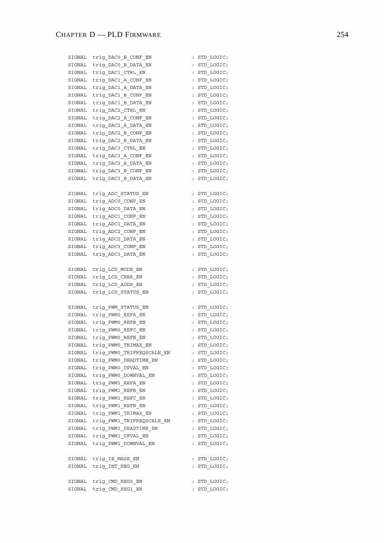
CHAPTER D — PLD FIRMWARE 254
SIGNAL trig_DAC0_B_CONF_EN : STD_LOGIC;
SIGNAL trig_DAC0_B_DATA_EN : STD_LOGIC;
SIGNAL trig_DAC1_CTRL_EN : STD_LOGIC;
SIGNAL trig_DAC1_A_CONF_EN : STD_LOGIC;
SIGNAL trig_DAC1_A_DATA_EN : STD_LOGIC;
SIGNAL trig_DAC1_B_CONF_EN : STD_LOGIC;
SIGNAL trig_DAC1_B_DATA_EN : STD_LOGIC;
SIGNAL trig_DAC2_CTRL_EN : STD_LOGIC;
SIGNAL trig_DAC2_A_CONF_EN : STD_LOGIC;
SIGNAL trig_DAC2_A_DATA_EN : STD_LOGIC;
SIGNAL trig_DAC2_B_CONF_EN : STD_LOGIC;
SIGNAL trig_DAC2_B_DATA_EN : STD_LOGIC;
SIGNAL trig_DAC3_CTRL_EN : STD_LOGIC;
SIGNAL trig_DAC3_A_CONF_EN : STD_LOGIC;
SIGNAL trig_DAC3_A_DATA_EN : STD_LOGIC;
SIGNAL trig_DAC3_B_CONF_EN : STD_LOGIC;
SIGNAL trig_DAC3_B_DATA_EN : STD_LOGIC;
SIGNAL trig_ADC_STATUS_EN : STD_LOGIC;
SIGNAL trig_ADC0_CONF_EN : STD_LOGIC;
SIGNAL trig_ADC0_DATA_EN : STD_LOGIC;
SIGNAL trig_ADC1_CONF_EN : STD_LOGIC;
SIGNAL trig_ADC1_DATA_EN : STD_LOGIC;
SIGNAL trig_ADC2_CONF_EN : STD_LOGIC;
SIGNAL trig_ADC2_DATA_EN : STD_LOGIC;
SIGNAL trig_ADC3_CONF_EN : STD_LOGIC;
SIGNAL trig_ADC3_DATA_EN : STD_LOGIC;
SIGNAL trig_LCD_MODE_EN : STD_LOGIC;
SIGNAL trig_LCD_CHAR_EN : STD_LOGIC;
SIGNAL trig_LCD_ADDR_EN : STD_LOGIC;
SIGNAL trig_LCD_STATUS_EN : STD_LOGIC;
SIGNAL trig_PWM_STATUS_EN : STD_LOGIC;
SIGNAL trig_PWM0_REFA_EN : STD_LOGIC;
SIGNAL trig_PWM0_REFB_EN : STD_LOGIC;
SIGNAL trig_PWM0_REFC_EN : STD_LOGIC;
SIGNAL trig_PWM0_REFN_EN : STD_LOGIC;
SIGNAL trig_PWM0_TRIMAX_EN : STD_LOGIC;
SIGNAL trig_PWM0_TRIFREQSCALE_EN : STD_LOGIC;
SIGNAL trig_PWM0_DEADTIME_EN : STD_LOGIC;
SIGNAL trig_PWM0_UPVAL_EN : STD_LOGIC;
SIGNAL trig_PWM0_DOWNVAL_EN : STD_LOGIC;
SIGNAL trig_PWM1_REFA_EN : STD_LOGIC;
SIGNAL trig_PWM1_REFB_EN : STD_LOGIC;
SIGNAL trig_PWM1_REFC_EN : STD_LOGIC;
SIGNAL trig_PWM1_REFN_EN : STD_LOGIC;
SIGNAL trig_PWM1_TRIMAX_EN : STD_LOGIC;
SIGNAL trig_PWM1_TRIFREQSCALE_EN : STD_LOGIC;
SIGNAL trig_PWM1_DEADTIME_EN : STD_LOGIC;
SIGNAL trig_PWM1_UPVAL_EN : STD_LOGIC;
SIGNAL trig_PWM1_DOWNVAL_EN : STD_LOGIC;
SIGNAL trig_IE_MASK_EN : STD_LOGIC;
SIGNAL trig_INT_REG_EN : STD_LOGIC;
SIGNAL trig_CMD_REG0_EN : STD_LOGIC;
SIGNAL trig_CMD_REG1_EN : STD_LOGIC;

CHAPTER D — PLD FIRMWARE 255
SIGNAL signal_ADDR : INTEGER RANGE 0 TO 1023;
SIGNAL dummy : STD_LOGIC_VECTOR( 9 DOWNTO 0 );
COMPONENT addr_element
GENERIC (
INT_ADDR : INTEGER RANGE 0 TO 1023 := 0
);
PORT (
EN : OUT STD_LOGIC;
ADDR : IN INTEGER RANGE 0 TO 1023;
nCS : IN STD_LOGIC;
CLK : IN STD_LOGIC;
RESET : IN STD_LOGIC
);
END COMPONENT;
BEGIN
signal_ADDR <= CONV_INTEGER( UNSIGNED( ADDR ) );
------------------------------------------------------------------------------------------
------------------------------------------------------------------------------------------
dac0_ctrl_en_map:
addr_element GENERIC MAP ( INT_ADDR => dac0_ctrl_addr )
PORT MAP ( EN => DAC0_CTRL_EN, ADDR => signal_ADDR,
nCS => FPGA_nCS, CLK => CLK, RESET => RESET );
dac0_a_conf_en_map:
addr_element GENERIC MAP ( INT_ADDR => dac0_a_conf_addr )
PORT MAP ( EN => DAC0_A_CONF_EN, ADDR => signal_ADDR,
nCS => FPGA_nCS, CLK => CLK, RESET => RESET );
dac0_a_data_en_map:
addr_element GENERIC MAP ( INT_ADDR => dac0_a_data_addr )
PORT MAP ( EN => DAC0_A_DATA_EN, ADDR => signal_ADDR,
nCS => FPGA_nCS, CLK => CLK, RESET => RESET );
dac0_b_conf_en_map:
addr_element GENERIC MAP ( INT_ADDR => dac0_b_conf_addr )
PORT MAP ( EN => DAC0_B_CONF_EN, ADDR => signal_ADDR,
nCS => FPGA_nCS, CLK => CLK, RESET => RESET );
dac0_b_data_en_map:
addr_element GENERIC MAP ( INT_ADDR => dac0_b_data_addr )
PORT MAP ( EN => DAC0_B_DATA_EN, ADDR => signal_ADDR,
nCS => FPGA_nCS, CLK => CLK, RESET => RESET );
------------------------------------------------------------------------------------------
dac1_ctrl_en_map:
addr_element GENERIC MAP ( INT_ADDR => dac1_ctrl_addr )
PORT MAP ( EN => DAC1_CTRL_EN, ADDR => signal_ADDR,
nCS => FPGA_nCS, CLK => CLK, RESET => RESET );

CHAPTER D — PLD FIRMWARE 256
dac1_a_conf_en_map:
addr_element GENERIC MAP ( INT_ADDR => dac1_a_conf_addr )
PORT MAP ( EN => DAC1_A_CONF_EN, ADDR => signal_ADDR,
nCS => FPGA_nCS, CLK => CLK, RESET => RESET );
dac1_a_data_en_map:
addr_element GENERIC MAP ( INT_ADDR => dac1_a_data_addr )
PORT MAP ( EN => DAC1_A_DATA_EN, ADDR => signal_ADDR,
nCS => FPGA_nCS, CLK => CLK, RESET => RESET );
dac1_b_conf_en_map:
addr_element GENERIC MAP ( INT_ADDR => dac1_b_conf_addr )
PORT MAP ( EN => DAC1_B_CONF_EN, ADDR => signal_ADDR,
nCS => FPGA_nCS, CLK => CLK, RESET => RESET );
dac1_b_data_en_map:
addr_element GENERIC MAP ( INT_ADDR => dac1_b_data_addr )
PORT MAP ( EN => DAC1_B_DATA_EN, ADDR => signal_ADDR,
nCS => FPGA_nCS, CLK => CLK, RESET => RESET );
------------------------------------------------------------------------------------------
dac2_ctrl_en_map:
addr_element GENERIC MAP ( INT_ADDR => dac2_ctrl_addr )
PORT MAP ( EN => DAC2_CTRL_EN, ADDR => signal_ADDR,
nCS => FPGA_nCS, CLK => CLK, RESET => RESET );
dac2_a_conf_en_map:
addr_element GENERIC MAP ( INT_ADDR => dac2_a_conf_addr )
PORT MAP ( EN => DAC2_A_CONF_EN, ADDR => signal_ADDR,
nCS => FPGA_nCS, CLK => CLK, RESET => RESET );
dac2_a_data_en_map:
addr_element GENERIC MAP ( INT_ADDR => dac2_a_data_addr )
PORT MAP ( EN => DAC2_A_DATA_EN, ADDR => signal_ADDR,
nCS => FPGA_nCS, CLK => CLK, RESET => RESET );
dac2_b_conf_en_map:
addr_element GENERIC MAP ( INT_ADDR => dac2_b_conf_addr )
PORT MAP ( EN => DAC2_B_CONF_EN, ADDR => signal_ADDR,
nCS => FPGA_nCS, CLK => CLK, RESET => RESET );
dac2_b_data_en_map:
addr_element GENERIC MAP ( INT_ADDR => dac2_b_data_addr )
PORT MAP ( EN => DAC2_B_DATA_EN, ADDR => signal_ADDR,
nCS => FPGA_nCS, CLK => CLK, RESET => RESET );
------------------------------------------------------------------------------------------
dac3_ctrl_en_map:
addr_element GENERIC MAP ( INT_ADDR => dac3_ctrl_addr )
PORT MAP ( EN => DAC3_CTRL_EN, ADDR => signal_ADDR,
nCS => FPGA_nCS, CLK => CLK, RESET => RESET );
dac3_a_conf_en_map:
addr_element GENERIC MAP ( INT_ADDR => dac3_a_conf_addr )
PORT MAP ( EN => DAC3_A_CONF_EN, ADDR => signal_ADDR,
nCS => FPGA_nCS, CLK => CLK, RESET => RESET );

CHAPTER D — PLD FIRMWARE 257
dac3_a_data_en_map:
addr_element GENERIC MAP ( INT_ADDR => dac3_a_data_addr )
PORT MAP ( EN => DAC3_A_DATA_EN, ADDR => signal_ADDR,
nCS => FPGA_nCS, CLK => CLK, RESET => RESET );
dac3_b_conf_en_map:
addr_element GENERIC MAP ( INT_ADDR => dac3_b_conf_addr )
PORT MAP ( EN => DAC3_B_CONF_EN, ADDR => signal_ADDR,
nCS => FPGA_nCS, CLK => CLK, RESET => RESET );
dac3_b_data_en_map:
addr_element GENERIC MAP ( INT_ADDR => dac3_b_data_addr )
PORT MAP ( EN => DAC3_B_DATA_EN, ADDR => signal_ADDR,
nCS => FPGA_nCS, CLK => CLK, RESET => RESET );
------------------------------------------------------------------------------------------
------------------------------------------------------------------------------------------
adc_status_en_map:
addr_element GENERIC MAP ( INT_ADDR => adc_status_addr )
PORT MAP ( EN => ADC_STATUS_EN, ADDR => signal_ADDR,
nCS => FPGA_nCS, CLK => CLK, RESET => RESET );
------------------------------------------------------------------------------------------
adc0_conf_en_map:
addr_element GENERIC MAP ( INT_ADDR => adc0_conf_addr )
PORT MAP ( EN => ADC0_CONF_EN, ADDR => signal_ADDR,
nCS => FPGA_nCS, CLK => CLK, RESET => RESET );
adc0_data_en_map:
addr_element GENERIC MAP ( INT_ADDR => adc0_data_addr )
PORT MAP ( EN => ADC0_DATA_EN, ADDR => signal_ADDR,
nCS => FPGA_nCS, CLK => CLK, RESET => RESET );
adc0_samp_chan0_en_proc:
addr_element GENERIC MAP ( INT_ADDR => adc0_samp_chan0_addr )
PORT MAP ( EN => ADC0_SAMP_CHAN0_EN, ADDR => signal_ADDR,
nCS => FPGA_nCS, CLK => CLK, RESET => RESET );
adc0_samp_chan1_en_proc:
addr_element GENERIC MAP ( INT_ADDR => adc0_samp_chan1_addr )
PORT MAP ( EN => ADC0_SAMP_CHAN1_EN, ADDR => signal_ADDR,
nCS => FPGA_nCS, CLK => CLK, RESET => RESET );
adc0_samp_chan2_en_proc:
addr_element GENERIC MAP ( INT_ADDR => adc0_samp_chan2_addr )
PORT MAP ( EN => ADC0_SAMP_CHAN2_EN, ADDR => signal_ADDR,
nCS => FPGA_nCS, CLK => CLK, RESET => RESET );
adc0_samp_chan3_en_proc:
addr_element GENERIC MAP ( INT_ADDR => adc0_samp_chan3_addr )
PORT MAP ( EN => ADC0_SAMP_CHAN3_EN, ADDR => signal_ADDR,
nCS => FPGA_nCS, CLK => CLK, RESET => RESET );
adc0_samp_chan4_en_proc:
addr_element GENERIC MAP ( INT_ADDR => adc0_samp_chan4_addr )
PORT MAP ( EN => ADC0_SAMP_CHAN4_EN, ADDR => signal_ADDR,

CHAPTER D — PLD FIRMWARE 258
nCS => FPGA_nCS, CLK => CLK, RESET => RESET );
adc0_samp_chan5_en_proc:
addr_element GENERIC MAP ( INT_ADDR => adc0_samp_chan5_addr )
PORT MAP ( EN => ADC0_SAMP_CHAN5_EN, ADDR => signal_ADDR,
nCS => FPGA_nCS, CLK => CLK, RESET => RESET );
adc0_samp_chan6_en_proc:
addr_element GENERIC MAP ( INT_ADDR => adc0_samp_chan6_addr )
PORT MAP ( EN => ADC0_SAMP_CHAN6_EN, ADDR => signal_ADDR,
nCS => FPGA_nCS, CLK => CLK, RESET => RESET );
adc0_samp_chan7_en_proc:
addr_element GENERIC MAP ( INT_ADDR => adc0_samp_chan7_addr )
PORT MAP ( EN => ADC0_SAMP_CHAN7_EN, ADDR => signal_ADDR,
nCS => FPGA_nCS, CLK => CLK, RESET => RESET );
------------------------------------------------------------------------------------------
adc1_conf_en_map:
addr_element GENERIC MAP ( INT_ADDR => adc1_conf_addr )
PORT MAP ( EN => ADC1_CONF_EN, ADDR => signal_ADDR,
nCS => FPGA_nCS, CLK => CLK, RESET => RESET );
adc1_data_en_map:
addr_element GENERIC MAP ( INT_ADDR => adc1_data_addr )
PORT MAP ( EN => ADC1_DATA_EN, ADDR => signal_ADDR,
nCS => FPGA_nCS, CLK => CLK, RESET => RESET );
adc1_samp_chan0_en_proc:
addr_element GENERIC MAP ( INT_ADDR => adc1_samp_chan0_addr )
PORT MAP ( EN => ADC1_SAMP_CHAN0_EN, ADDR => signal_ADDR,
nCS => FPGA_nCS, CLK => CLK, RESET => RESET );
adc1_samp_chan1_en_proc:
addr_element GENERIC MAP ( INT_ADDR => adc1_samp_chan1_addr )
PORT MAP ( EN => ADC1_SAMP_CHAN1_EN, ADDR => signal_ADDR,
nCS => FPGA_nCS, CLK => CLK, RESET => RESET );
adc1_samp_chan2_en_proc:
addr_element GENERIC MAP ( INT_ADDR => adc1_samp_chan2_addr )
PORT MAP ( EN => ADC1_SAMP_CHAN2_EN, ADDR => signal_ADDR,
nCS => FPGA_nCS, CLK => CLK, RESET => RESET );
adc1_samp_chan3_en_proc:
addr_element GENERIC MAP ( INT_ADDR => adc1_samp_chan3_addr )
PORT MAP ( EN => ADC1_SAMP_CHAN3_EN, ADDR => signal_ADDR,
nCS => FPGA_nCS, CLK => CLK, RESET => RESET );
adc1_samp_chan4_en_proc:
addr_element GENERIC MAP ( INT_ADDR => adc1_samp_chan4_addr )
PORT MAP ( EN => ADC1_SAMP_CHAN4_EN, ADDR => signal_ADDR,
nCS => FPGA_nCS, CLK => CLK, RESET => RESET );
adc1_samp_chan5_en_proc:
addr_element GENERIC MAP ( INT_ADDR => adc1_samp_chan5_addr )
PORT MAP ( EN => ADC1_SAMP_CHAN5_EN, ADDR => signal_ADDR,
nCS => FPGA_nCS, CLK => CLK, RESET => RESET );

CHAPTER D — PLD FIRMWARE 259
adc1_samp_chan6_en_proc:
addr_element GENERIC MAP ( INT_ADDR => adc1_samp_chan6_addr )
PORT MAP ( EN => ADC1_SAMP_CHAN6_EN, ADDR => signal_ADDR,
nCS => FPGA_nCS, CLK => CLK, RESET => RESET );
adc1_samp_chan7_en_proc:
addr_element GENERIC MAP ( INT_ADDR => adc1_samp_chan7_addr )
PORT MAP ( EN => ADC1_SAMP_CHAN7_EN, ADDR => signal_ADDR,
nCS => FPGA_nCS, CLK => CLK, RESET => RESET );
------------------------------------------------------------------------------------------
adc2_conf_en_map:
addr_element GENERIC MAP ( INT_ADDR => adc2_conf_addr )
PORT MAP ( EN => ADC2_CONF_EN, ADDR => signal_ADDR,
nCS => FPGA_nCS, CLK => CLK, RESET => RESET );
adc2_data_en_map:
addr_element GENERIC MAP ( INT_ADDR => adc2_data_addr )
PORT MAP ( EN => ADC2_DATA_EN, ADDR => signal_ADDR,
nCS => FPGA_nCS, CLK => CLK, RESET => RESET );
adc2_samp_chan0_en_proc:
addr_element GENERIC MAP ( INT_ADDR => adc2_samp_chan0_addr )
PORT MAP ( EN => ADC2_SAMP_CHAN0_EN, ADDR => signal_ADDR,
nCS => FPGA_nCS, CLK => CLK, RESET => RESET );
adc2_samp_chan1_en_proc:
addr_element GENERIC MAP ( INT_ADDR => adc2_samp_chan1_addr )
PORT MAP ( EN => ADC2_SAMP_CHAN1_EN, ADDR => signal_ADDR,
nCS => FPGA_nCS, CLK => CLK, RESET => RESET );
adc2_samp_chan2_en_proc:
addr_element GENERIC MAP ( INT_ADDR => adc2_samp_chan2_addr )
PORT MAP ( EN => ADC2_SAMP_CHAN2_EN, ADDR => signal_ADDR,
nCS => FPGA_nCS, CLK => CLK, RESET => RESET );
adc2_samp_chan3_en_proc:
addr_element GENERIC MAP ( INT_ADDR => adc2_samp_chan3_addr )
PORT MAP ( EN => ADC2_SAMP_CHAN3_EN, ADDR => signal_ADDR,
nCS => FPGA_nCS, CLK => CLK, RESET => RESET );
adc2_samp_chan4_en_proc:
addr_element GENERIC MAP ( INT_ADDR => adc2_samp_chan4_addr )
PORT MAP ( EN => ADC2_SAMP_CHAN4_EN, ADDR => signal_ADDR,
nCS => FPGA_nCS, CLK => CLK, RESET => RESET );
adc2_samp_chan5_en_proc:
addr_element GENERIC MAP ( INT_ADDR => adc2_samp_chan5_addr )
PORT MAP ( EN => ADC2_SAMP_CHAN5_EN, ADDR => signal_ADDR,
nCS => FPGA_nCS, CLK => CLK, RESET => RESET );
adc2_samp_chan6_en_proc:
addr_element GENERIC MAP ( INT_ADDR => adc2_samp_chan6_addr )
PORT MAP ( EN => ADC2_SAMP_CHAN6_EN, ADDR => signal_ADDR,
nCS => FPGA_nCS, CLK => CLK, RESET => RESET );
adc2_samp_chan7_en_proc:
addr_element GENERIC MAP ( INT_ADDR => adc2_samp_chan7_addr )

CHAPTER D — PLD FIRMWARE 260
PORT MAP ( EN => ADC2_SAMP_CHAN7_EN, ADDR => signal_ADDR,
nCS => FPGA_nCS, CLK => CLK, RESET => RESET );
------------------------------------------------------------------------------------------
adc3_conf_en_map:
addr_element GENERIC MAP ( INT_ADDR => adc3_conf_addr )
PORT MAP ( EN => ADC3_CONF_EN, ADDR => signal_ADDR,
nCS => FPGA_nCS, CLK => CLK, RESET => RESET );
adc3_data_en_map:
addr_element GENERIC MAP ( INT_ADDR => adc3_data_addr )
PORT MAP ( EN => ADC3_DATA_EN, ADDR => signal_ADDR,
nCS => FPGA_nCS, CLK => CLK, RESET => RESET );
adc3_samp_chan0_en_proc:
addr_element GENERIC MAP ( INT_ADDR => adc3_samp_chan0_addr )
PORT MAP ( EN => ADC3_SAMP_CHAN0_EN, ADDR => signal_ADDR,
nCS => FPGA_nCS, CLK => CLK, RESET => RESET );
adc3_samp_chan1_en_proc:
addr_element GENERIC MAP ( INT_ADDR => adc3_samp_chan1_addr )
PORT MAP ( EN => ADC3_SAMP_CHAN1_EN, ADDR => signal_ADDR,
nCS => FPGA_nCS, CLK => CLK, RESET => RESET );
adc3_samp_chan2_en_proc:
addr_element GENERIC MAP ( INT_ADDR => adc3_samp_chan2_addr )
PORT MAP ( EN => ADC3_SAMP_CHAN2_EN, ADDR => signal_ADDR,
nCS => FPGA_nCS, CLK => CLK, RESET => RESET );
adc3_samp_chan3_en_proc:
addr_element GENERIC MAP ( INT_ADDR => adc3_samp_chan3_addr )
PORT MAP ( EN => ADC3_SAMP_CHAN3_EN, ADDR => signal_ADDR,
nCS => FPGA_nCS, CLK => CLK, RESET => RESET );
adc3_samp_chan4_en_proc:
addr_element GENERIC MAP ( INT_ADDR => adc3_samp_chan4_addr )
PORT MAP ( EN => ADC3_SAMP_CHAN4_EN, ADDR => signal_ADDR,
nCS => FPGA_nCS, CLK => CLK, RESET => RESET );
adc3_samp_chan5_en_proc:
addr_element GENERIC MAP ( INT_ADDR => adc3_samp_chan5_addr )
PORT MAP ( EN => ADC3_SAMP_CHAN5_EN, ADDR => signal_ADDR,
nCS => FPGA_nCS, CLK => CLK, RESET => RESET );
adc3_samp_chan6_en_proc:
addr_element GENERIC MAP ( INT_ADDR => adc3_samp_chan6_addr )
PORT MAP ( EN => ADC3_SAMP_CHAN6_EN, ADDR => signal_ADDR,
nCS => FPGA_nCS, CLK => CLK, RESET => RESET );
adc3_samp_chan7_en_proc:
addr_element GENERIC MAP ( INT_ADDR => adc3_samp_chan7_addr )
PORT MAP ( EN => ADC3_SAMP_CHAN7_EN, ADDR => signal_ADDR,
nCS => FPGA_nCS, CLK => CLK, RESET => RESET );
------------------------------------------------------------------------------------------
------------------------------------------------------------------------------------------
lcd_mode_en_map:

CHAPTER D — PLD FIRMWARE 261
addr_element GENERIC MAP ( INT_ADDR => lcd_mode_addr )
PORT MAP ( EN => LCD_MODE_EN, ADDR => signal_ADDR,
nCS => FPGA_nCS, CLK => CLK, RESET => RESET );
lcd_char_en_map:
addr_element GENERIC MAP ( INT_ADDR => lcd_char_addr )
PORT MAP ( EN => LCD_CHAR_EN, ADDR => signal_ADDR,
nCS => FPGA_nCS, CLK => CLK, RESET => RESET );
lcd_addr_en_map:
addr_element GENERIC MAP ( INT_ADDR => lcd_addr_addr )
PORT MAP ( EN => LCD_ADDR_EN, ADDR => signal_ADDR,
nCS => FPGA_nCS, CLK => CLK, RESET => RESET );
lcd_status_en_map:
addr_element GENERIC MAP ( INT_ADDR => lcd_status_addr )
PORT MAP ( EN => LCD_STATUS_EN, ADDR => signal_ADDR,
nCS => FPGA_nCS, CLK => CLK, RESET => RESET );
------------------------------------------------------------------------------------------
------------------------------------------------------------------------------------------
keyval_en_map:
addr_element GENERIC MAP ( INT_ADDR => keyval_addr )
PORT MAP ( EN => KEYVAL_EN, ADDR => signal_ADDR,
nCS => FPGA_nCS, CLK => CLK, RESET => RESET );
------------------------------------------------------------------------------------------
------------------------------------------------------------------------------------------
pwm_status_en_map:
addr_element GENERIC MAP ( INT_ADDR => pwm_status_addr )
PORT MAP ( EN => PWM_STATUS_EN, ADDR => signal_ADDR,
nCS => FPGA_nCS, CLK => CLK, RESET => RESET );
------------------------------------------------------------------------------------------
pwm0_refa_en_map:
addr_element GENERIC MAP ( INT_ADDR => pwm0_refa_addr )
PORT MAP ( EN => PWM0_REFA_EN, ADDR => signal_ADDR,
nCS => FPGA_nCS, CLK => CLK, RESET => RESET );
pwm0_refb_en_map:
addr_element GENERIC MAP ( INT_ADDR => pwm0_refb_addr )
PORT MAP ( EN => PWM0_REFB_EN, ADDR => signal_ADDR,
nCS => FPGA_nCS, CLK => CLK, RESET => RESET );
pwm0_refc_en_map:
addr_element GENERIC MAP ( INT_ADDR => pwm0_refc_addr )
PORT MAP ( EN => PWM0_REFC_EN, ADDR => signal_ADDR,
nCS => FPGA_nCS, CLK => CLK, RESET => RESET );
pwm0_refn_en_map:
addr_element GENERIC MAP ( INT_ADDR => pwm0_refn_addr )
PORT MAP ( EN => PWM0_REFN_EN, ADDR => signal_ADDR,
nCS => FPGA_nCS, CLK => CLK, RESET => RESET );
pwm0_trimax_en_map:
addr_element GENERIC MAP ( INT_ADDR => pwm0_trimax_addr )
PORT MAP ( EN => PWM0_TRIMAX_EN, ADDR => signal_ADDR,

CHAPTER D — PLD FIRMWARE 262
nCS => FPGA_nCS, CLK => CLK, RESET => RESET );
pwm0_trifreqscale_en_map:
addr_element GENERIC MAP ( INT_ADDR => pwm0_trifreqscale_addr )
PORT MAP ( EN => PWM0_TRIFREQSCALE_EN, ADDR => signal_ADDR,
nCS => FPGA_nCS, CLK => CLK, RESET => RESET );
pwm0_deadtime_en_map:
addr_element GENERIC MAP ( INT_ADDR => pwm0_deadtime_addr )
PORT MAP ( EN => PWM0_DEADTIME_EN, ADDR => signal_ADDR,
nCS => FPGA_nCS, CLK => CLK, RESET => RESET );
pwm0_upval_en_map:
addr_element GENERIC MAP ( INT_ADDR => pwm0_upval_addr )
PORT MAP ( EN => PWM0_UPVAL_EN, ADDR => signal_ADDR,
nCS => FPGA_nCS, CLK => CLK, RESET => RESET );
pwm0_downval_en_map:
addr_element GENERIC MAP ( INT_ADDR => pwm0_downval_addr )
PORT MAP ( EN => PWM0_DOWNVAL_EN, ADDR => signal_ADDR,
nCS => FPGA_nCS, CLK => CLK, RESET => RESET );
------------------------------------------------------------------------------------------
pwm1_refa_en_map:
addr_element GENERIC MAP ( INT_ADDR => pwm1_refa_addr )
PORT MAP ( EN => PWM1_REFA_EN, ADDR => signal_ADDR,
nCS => FPGA_nCS, CLK => CLK, RESET => RESET );
pwm1_refb_en_map:
addr_element GENERIC MAP ( INT_ADDR => pwm1_refb_addr )
PORT MAP ( EN => PWM1_REFB_EN, ADDR => signal_ADDR,
nCS => FPGA_nCS, CLK => CLK, RESET => RESET );
pwm1_refc_en_map:
addr_element GENERIC MAP ( INT_ADDR => pwm1_refc_addr )
PORT MAP ( EN => PWM1_REFC_EN, ADDR => signal_ADDR,
nCS => FPGA_nCS, CLK => CLK, RESET => RESET );
pwm1_refn_en_map:
addr_element GENERIC MAP ( INT_ADDR => pwm1_refn_addr )
PORT MAP ( EN => PWM1_REFN_EN, ADDR => signal_ADDR,
nCS => FPGA_nCS, CLK => CLK, RESET => RESET );
pwm1_trimax_en_map:
addr_element GENERIC MAP ( INT_ADDR => pwm1_trimax_addr )
PORT MAP ( EN => PWM1_TRIMAX_EN, ADDR => signal_ADDR,
nCS => FPGA_nCS, CLK => CLK, RESET => RESET );
pwm1_trifreqscale_en_map:
addr_element GENERIC MAP ( INT_ADDR => pwm1_trifreqscale_addr )
PORT MAP ( EN => PWM1_TRIFREQSCALE_EN, ADDR => signal_ADDR,
nCS => FPGA_nCS, CLK => CLK, RESET => RESET );
pwm1_deadtime_en_map:
addr_element GENERIC MAP ( INT_ADDR => pwm1_deadtime_addr )
PORT MAP ( EN => PWM1_DEADTIME_EN, ADDR => signal_ADDR,
nCS => FPGA_nCS, CLK => CLK, RESET => RESET );

CHAPTER D — PLD FIRMWARE 263
pwm1_upval_en_map:
addr_element GENERIC MAP ( INT_ADDR => pwm1_upval_addr )
PORT MAP ( EN => PWM1_UPVAL_EN, ADDR => signal_ADDR,
nCS => FPGA_nCS, CLK => CLK, RESET => RESET );
pwm1_downval_en_map:
addr_element GENERIC MAP ( INT_ADDR => pwm1_downval_addr )
PORT MAP ( EN => PWM1_DOWNVAL_EN, ADDR => signal_ADDR,
nCS => FPGA_nCS, CLK => CLK, RESET => RESET );
------------------------------------------------------------------------------------------
pwm_err_top_en_map:
addr_element GENERIC MAP ( INT_ADDR => pwm_err_top_addr )
PORT MAP ( EN => PWM_ERR_TOP_EN, ADDR => signal_ADDR,
nCS => FPGA_nCS, CLK => CLK, RESET => RESET );
pwm_err_bot_en_map:
addr_element GENERIC MAP ( INT_ADDR => pwm_err_bot_addr )
PORT MAP ( EN => PWM_ERR_BOT_EN, ADDR => signal_ADDR,
nCS => FPGA_nCS, CLK => CLK, RESET => RESET );
------------------------------------------------------------------------------------------
------------------------------------------------------------------------------------------
int_en_en_map:
addr_element GENERIC MAP ( INT_ADDR => int_en_addr )
PORT MAP ( EN => INT_EN_EN, ADDR => signal_ADDR,
nCS => FPGA_nCS, CLK => CLK, RESET => RESET );
------------------------------------------------------------------------------------------
int_reg_en_map:
addr_element GENERIC MAP ( INT_ADDR => int_reg_addr )
PORT MAP ( EN => INT_REG_EN, ADDR => signal_ADDR,
nCS => FPGA_nCS, CLK => CLK, RESET => RESET );
------------------------------------------------------------------------------------------
------------------------------------------------------------------------------------------
cmd_reg0_en_map:
addr_element GENERIC MAP ( INT_ADDR => cmd_reg0_addr )
PORT MAP ( EN => CMD_REG0_EN, ADDR => signal_ADDR,
nCS => FPGA_nCS, CLK => CLK, RESET => RESET );
cmd_reg1_en_map:
addr_element GENERIC MAP ( INT_ADDR => cmd_reg1_addr )
PORT MAP ( EN => CMD_REG1_EN, ADDR => signal_ADDR,
nCS => FPGA_nCS, CLK => CLK, RESET => RESET );
------------------------------------------------------------------------------------------
------------------------------------------------------------------------------------------
END a;

CHAPTER D — PLD FIRMWARE 264
D.2.3 VHDL Code for the Addr Element Module of FPGA Analog-- FPGA Analog - ADDR_Element 2002-11-07
LIBRARY ieee;
USE ieee.std_logic_1164.all;
USE ieee.std_logic_arith.all;
ENTITY addr_element IS
GENERIC (
INT_ADDR : INTEGER RANGE 0 TO 1023 := 0
);
PORT (
EN : OUT STD_LOGIC;
ADDR : IN INTEGER RANGE 0 TO 1023;
nCS : IN STD_LOGIC;
CLK : IN STD_LOGIC;
RESET : IN STD_LOGIC
);
END addr_element;
ARCHITECTURE a OF addr_element IS
BEGIN
reg_proc:
PROCESS ( CLK, RESET )
BEGIN
IF ( RESET = ’1’ ) THEN
EN <= ’0’;
ELSIF ( CLK’event )and( CLK = ’1’ ) THEN
IF ( nCS = ’0’ )and( INT_ADDR = ADDR ) THEN
EN <= ’1’;
ELSE
EN <= ’0’;
END IF;
END IF;
END PROCESS reg_proc;
END a;

CHAPTER D — PLD FIRMWARE 265
D.2.4 VHDL Code for the Command Ctrl Module of FPGA Analog-- FPGA Analog - Command Controller 2002-11-07
LIBRARY ieee;
USE ieee.std_logic_1164.all;
USE ieee.std_logic_arith.all;
ENTITY Command_Ctrl IS
PORT (
CMD_REG0 : IN STD_LOGIC_VECTOR ( 6 DOWNTO 0 );
CMD_REG1 : IN STD_LOGIC_VECTOR ( 5 DOWNTO 0 );
RESET : IN STD_LOGIC;
CLK : IN STD_LOGIC;
DAC0_nLOAD : OUT STD_LOGIC;
DAC1_nLOAD : OUT STD_LOGIC;
DAC2_nLOAD : OUT STD_LOGIC;
DAC3_nLOAD : OUT STD_LOGIC;
ADC0_nEN : OUT STD_LOGIC;
ADC1_nEN : OUT STD_LOGIC;
ADC2_nEN : OUT STD_LOGIC;
ADC3_nEN : OUT STD_LOGIC;
LCD_UPDATE_MODE : OUT STD_LOGIC;
LCD_UPDATE_DATA : OUT STD_LOGIC;
LCD_RESET : OUT STD_LOGIC;
PWM0_nEN : OUT STD_LOGIC;
PWM1_nEN : OUT STD_LOGIC
);
END Command_Ctrl;
ARCHITECTURE a OF Command_Ctrl IS
TYPE statetype IS ( state0, state1, state2, state3 );
-- Current and next state of the type 0 command state machine
SIGNAL sm0_state : statetype;
SIGNAL nextsm0_state : statetype;
-- Start signal for the type 0 command state machine
SIGNAL start_sm0 : STD_LOGIC;
-- New and previous command output register for type 0 commands
SIGNAL signal_cmd_reg0 : STD_LOGIC_VECTOR ( 6 DOWNTO 0 );
SIGNAL signal_prevcmd_reg0 : STD_LOGIC_VECTOR ( 6 DOWNTO 0 );
-- New command output register for type 0 commands
SIGNAL signal_cmd_reg1 : STD_LOGIC_VECTOR ( 5 DOWNTO 0 );
BEGIN
DAC0_nLOAD <= signal_cmd_reg0(0);
DAC1_nLOAD <= signal_cmd_reg0(1);
DAC2_nLOAD <= signal_cmd_reg0(2);
DAC3_nLOAD <= signal_cmd_reg0(3);

CHAPTER D — PLD FIRMWARE 266
LCD_UPDATE_MODE <= signal_cmd_reg0(4);
LCD_UPDATE_DATA <= signal_cmd_reg0(5);
LCD_RESET <= signal_cmd_reg0(6);
ADC0_nEN <= signal_cmd_reg1(0);
ADC1_nEN <= signal_cmd_reg1(1);
ADC2_nEN <= signal_cmd_reg1(2);
ADC3_nEN <= signal_cmd_reg1(3);
PWM0_nEN <= signal_cmd_reg1(4);
PWM1_nEN <= signal_cmd_reg1(5);
------------------------------------------------------------------------------------------
reg0_proc:
PROCESS ( CLK, RESET )
BEGIN
IF ( RESET = ’1’ ) THEN
signal_cmd_reg0 <= "1111111";
ELSIF ( CLK’event )and( CLK = ’1’ ) THEN
IF ( sm0_state = state0 ) THEN
signal_cmd_reg0 <= "1111111";
ELSIF ( sm0_state = state1 ) THEN
signal_cmd_reg0 <= not( CMD_REG0 );
END IF;
END IF;
END PROCESS reg0_proc;
------------------------------------------------------------------------------------------
reg1_proc:
PROCESS ( CLK, RESET )
BEGIN
IF ( RESET = ’1’ ) THEN
signal_cmd_reg1 <= "111111";
ELSIF ( CLK’event )and( CLK = ’1’ ) THEN
signal_cmd_reg1 <= not( CMD_REG1 );
END IF;
END PROCESS reg1_proc;
------------------------------------------------------------------------------------------
sm0_proc:
PROCESS ( sm0_state )
BEGIN
CASE sm0_state IS
WHEN state0 =>
nextsm0_state <= state1;

CHAPTER D — PLD FIRMWARE 267
WHEN state1 =>
nextsm0_state <= state2;
WHEN state2 =>
nextsm0_state <= state3;
WHEN state3 =>
nextsm0_state <= state0;
END CASE;
END PROCESS sm0_proc;
------------------------------------------------------------------------------------------
sm0_ctrl_proc:
PROCESS ( CLK, RESET )
BEGIN
IF ( RESET = ’1’ ) THEN
sm0_state <= state0;
ELSIF ( CLK’event )and( CLK = ’1’ ) THEN
IF ( sm0_state /= state0 )or( start_sm0 = ’1’ ) THEN
sm0_state <= nextsm0_state;
END IF;
END IF;
END PROCESS sm0_ctrl_proc;
------------------------------------------------------------------------------------------
start_sm0_proc:
PROCESS ( CLK, RESET, sm0_state )
BEGIN
IF ( RESET = ’1’ ) THEN
start_sm0 <= ’0’;
signal_prevcmd_reg0 <= "0000000";
ELSIF ( CLK’event )and( CLK = ’1’ ) THEN
IF ( CMD_REG0 = "0000000" ) THEN -- No command received
start_sm0 <= ’0’;
signal_prevcmd_reg0 <= "0000000";
ELSIF ( CMD_REG0 /= signal_prevcmd_reg0 ) THEN -- New command received
start_sm0 <= ’1’;
signal_prevcmd_reg0 <= CMD_REG0;
ELSE -- No new command received
start_sm0 <= ’0’;
signal_prevcmd_reg0 <= signal_prevcmd_reg0;
END IF;
END IF;
END PROCESS start_sm0_proc;

CHAPTER D — PLD FIRMWARE 268
END a;

CHAPTER D — PLD FIRMWARE 269
D.2.5 VHDL Code for the Data Ctrl Module of FPGA Analog-- FPGA Analog - Data Controller 2002-11-07
LIBRARY ieee;
USE ieee.std_logic_1164.all;
USE ieee.std_logic_arith.all;
ENTITY Data_Ctrl IS
PORT (
DAC0_CTRL_DATA : OUT STD_LOGIC_VECTOR ( 1 DOWNTO 0 );
DAC0_A_DATA : OUT STD_LOGIC_VECTOR ( 11 DOWNTO 0 );
DAC0_A_CONF_DATA : OUT STD_LOGIC_VECTOR ( 2 DOWNTO 0 );
DAC0_B_DATA : OUT STD_LOGIC_VECTOR ( 11 DOWNTO 0 );
DAC0_B_CONF_DATA : OUT STD_LOGIC_VECTOR ( 2 DOWNTO 0 );
DAC1_CTRL_DATA : OUT STD_LOGIC_VECTOR ( 1 DOWNTO 0 );
DAC1_A_DATA : OUT STD_LOGIC_VECTOR ( 11 DOWNTO 0 );
DAC1_A_CONF_DATA : OUT STD_LOGIC_VECTOR ( 2 DOWNTO 0 );
DAC1_B_DATA : OUT STD_LOGIC_VECTOR ( 11 DOWNTO 0 );
DAC1_B_CONF_DATA : OUT STD_LOGIC_VECTOR ( 2 DOWNTO 0 );
DAC2_CTRL_DATA : OUT STD_LOGIC_VECTOR ( 1 DOWNTO 0 );
DAC2_A_DATA : OUT STD_LOGIC_VECTOR ( 11 DOWNTO 0 );
DAC2_A_CONF_DATA : OUT STD_LOGIC_VECTOR ( 2 DOWNTO 0 );
DAC2_B_DATA : OUT STD_LOGIC_VECTOR ( 11 DOWNTO 0 );
DAC2_B_CONF_DATA : OUT STD_LOGIC_VECTOR ( 2 DOWNTO 0 );
DAC3_CTRL_DATA : OUT STD_LOGIC_VECTOR ( 1 DOWNTO 0 );
DAC3_A_DATA : OUT STD_LOGIC_VECTOR ( 11 DOWNTO 0 );
DAC3_A_CONF_DATA : OUT STD_LOGIC_VECTOR ( 2 DOWNTO 0 );
DAC3_B_DATA : OUT STD_LOGIC_VECTOR ( 11 DOWNTO 0 );
DAC3_B_CONF_DATA : OUT STD_LOGIC_VECTOR ( 2 DOWNTO 0 );
ADC0_DATA : IN STD_LOGIC_VECTOR ( 12 DOWNTO 0 );
ADC0_DATA_RDY : IN STD_LOGIC;
ADC0_CONF_DATA : OUT STD_LOGIC_VECTOR ( 9 DOWNTO 0 );
ADC0_SAMP_CHAN0 : OUT STD_LOGIC_VECTOR ( 2 DOWNTO 0 );
ADC0_SAMP_CHAN1 : OUT STD_LOGIC_VECTOR ( 2 DOWNTO 0 );
ADC0_SAMP_CHAN2 : OUT STD_LOGIC_VECTOR ( 2 DOWNTO 0 );
ADC0_SAMP_CHAN3 : OUT STD_LOGIC_VECTOR ( 2 DOWNTO 0 );
ADC0_SAMP_CHAN4 : OUT STD_LOGIC_VECTOR ( 2 DOWNTO 0 );
ADC0_SAMP_CHAN5 : OUT STD_LOGIC_VECTOR ( 2 DOWNTO 0 );
ADC0_SAMP_CHAN6 : OUT STD_LOGIC_VECTOR ( 2 DOWNTO 0 );
ADC0_SAMP_CHAN7 : OUT STD_LOGIC_VECTOR ( 2 DOWNTO 0 );
ADC1_DATA : IN STD_LOGIC_VECTOR ( 12 DOWNTO 0 );
ADC1_DATA_RDY : IN STD_LOGIC;
ADC1_CONF_DATA : OUT STD_LOGIC_VECTOR ( 9 DOWNTO 0 );
ADC1_SAMP_CHAN0 : OUT STD_LOGIC_VECTOR ( 2 DOWNTO 0 );
ADC1_SAMP_CHAN1 : OUT STD_LOGIC_VECTOR ( 2 DOWNTO 0 );
ADC1_SAMP_CHAN2 : OUT STD_LOGIC_VECTOR ( 2 DOWNTO 0 );
ADC1_SAMP_CHAN3 : OUT STD_LOGIC_VECTOR ( 2 DOWNTO 0 );
ADC1_SAMP_CHAN4 : OUT STD_LOGIC_VECTOR ( 2 DOWNTO 0 );
ADC1_SAMP_CHAN5 : OUT STD_LOGIC_VECTOR ( 2 DOWNTO 0 );
ADC1_SAMP_CHAN6 : OUT STD_LOGIC_VECTOR ( 2 DOWNTO 0 );
ADC1_SAMP_CHAN7 : OUT STD_LOGIC_VECTOR ( 2 DOWNTO 0 );
CHAPTER D — PLD FIRMWARE 270
ADC2_DATA : IN STD_LOGIC_VECTOR ( 12 DOWNTO 0 );
ADC2_DATA_RDY : IN STD_LOGIC;
ADC2_CONF_DATA : OUT STD_LOGIC_VECTOR ( 9 DOWNTO 0 );
ADC2_SAMP_CHAN0 : OUT STD_LOGIC_VECTOR ( 2 DOWNTO 0 );
ADC2_SAMP_CHAN1 : OUT STD_LOGIC_VECTOR ( 2 DOWNTO 0 );
ADC2_SAMP_CHAN2 : OUT STD_LOGIC_VECTOR ( 2 DOWNTO 0 );
ADC2_SAMP_CHAN3 : OUT STD_LOGIC_VECTOR ( 2 DOWNTO 0 );
ADC2_SAMP_CHAN4 : OUT STD_LOGIC_VECTOR ( 2 DOWNTO 0 );
ADC2_SAMP_CHAN5 : OUT STD_LOGIC_VECTOR ( 2 DOWNTO 0 );
ADC2_SAMP_CHAN6 : OUT STD_LOGIC_VECTOR ( 2 DOWNTO 0 );
ADC2_SAMP_CHAN7 : OUT STD_LOGIC_VECTOR ( 2 DOWNTO 0 );
ADC3_DATA : IN STD_LOGIC_VECTOR ( 12 DOWNTO 0 );
ADC3_DATA_RDY : IN STD_LOGIC;
ADC3_CONF_DATA : OUT STD_LOGIC_VECTOR ( 9 DOWNTO 0 );
ADC3_SAMP_CHAN0 : OUT STD_LOGIC_VECTOR ( 2 DOWNTO 0 );
ADC3_SAMP_CHAN1 : OUT STD_LOGIC_VECTOR ( 2 DOWNTO 0 );
ADC3_SAMP_CHAN2 : OUT STD_LOGIC_VECTOR ( 2 DOWNTO 0 );
ADC3_SAMP_CHAN3 : OUT STD_LOGIC_VECTOR ( 2 DOWNTO 0 );
ADC3_SAMP_CHAN4 : OUT STD_LOGIC_VECTOR ( 2 DOWNTO 0 );
ADC3_SAMP_CHAN5 : OUT STD_LOGIC_VECTOR ( 2 DOWNTO 0 );
ADC3_SAMP_CHAN6 : OUT STD_LOGIC_VECTOR ( 2 DOWNTO 0 );
ADC3_SAMP_CHAN7 : OUT STD_LOGIC_VECTOR ( 2 DOWNTO 0 );
LCD_MODE_DATA : OUT STD_LOGIC_VECTOR ( 7 DOWNTO 0 );
LCD_CHAR : OUT STD_LOGIC_VECTOR ( 7 DOWNTO 0 );
LCD_ADDR : OUT STD_LOGIC_VECTOR ( 6 DOWNTO 0 );
LCD_RDYnBSY : IN STD_LOGIC;
KEYVAL : IN STD_LOGIC_VECTOR ( 3 DOWNTO 0 );
PWM0_REFA : OUT STD_LOGIC_VECTOR ( 9 DOWNTO 0 );
PWM0_REFB : OUT STD_LOGIC_VECTOR ( 9 DOWNTO 0 );
PWM0_REFC : OUT STD_LOGIC_VECTOR ( 9 DOWNTO 0 );
PWM0_REFN : OUT STD_LOGIC_VECTOR ( 9 DOWNTO 0 );
PWM0_TRIMAX : OUT STD_LOGIC_VECTOR ( 9 DOWNTO 0 );
PWM0_FREQSCALE : OUT STD_LOGIC_VECTOR ( 9 DOWNTO 0 );
PWM0_DEADTIME : OUT STD_LOGIC_VECTOR ( 9 DOWNTO 0 );
PWM0_COMPUPVAL : OUT STD_LOGIC_VECTOR ( 9 DOWNTO 0 );
PWM0_COMPDOWNVAL : OUT STD_LOGIC_VECTOR ( 9 DOWNTO 0 );
PWM0_COMPUP : IN STD_LOGIC;
PWM0_COMPDOWN : IN STD_LOGIC;
PWM0_RAMPDIR : IN STD_LOGIC;
PWM0_COUNTERZERO : IN STD_LOGIC;
PWM1_REFA : OUT STD_LOGIC_VECTOR ( 9 DOWNTO 0 );
PWM1_REFB : OUT STD_LOGIC_VECTOR ( 9 DOWNTO 0 );
PWM1_REFC : OUT STD_LOGIC_VECTOR ( 9 DOWNTO 0 );
PWM1_REFN : OUT STD_LOGIC_VECTOR ( 9 DOWNTO 0 );
PWM1_TRIMAX : OUT STD_LOGIC_VECTOR ( 9 DOWNTO 0 );
PWM1_FREQSCALE : OUT STD_LOGIC_VECTOR ( 9 DOWNTO 0 );
PWM1_DEADTIME : OUT STD_LOGIC_VECTOR ( 9 DOWNTO 0 );
PWM1_COMPUPVAL : OUT STD_LOGIC_VECTOR ( 9 DOWNTO 0 );
PWM1_COMPDOWNVAL : OUT STD_LOGIC_VECTOR ( 9 DOWNTO 0 );
PWM1_COMPUP : IN STD_LOGIC;
PWM1_COMPDOWN : IN STD_LOGIC;
PWM1_RAMPDIR : IN STD_LOGIC;
PWM1_COUNTERZERO : IN STD_LOGIC;
CHAPTER D — PLD FIRMWARE 271
PWM_ERR_TOP : IN STD_LOGIC_VECTOR ( 8 DOWNTO 0 );
PWM_ERR_BOT : IN STD_LOGIC_VECTOR ( 8 DOWNTO 0 );
INT_EN : OUT STD_LOGIC_VECTOR ( 14 DOWNTO 0 );
INT_REG : IN STD_LOGIC_VECTOR ( 5 DOWNTO 0 );
CMD_REG0 : OUT STD_LOGIC_VECTOR ( 6 DOWNTO 0 );
CMD_REG1 : OUT STD_LOGIC_VECTOR ( 5 DOWNTO 0 );
DAC0_CTRL_EN : IN STD_LOGIC;
DAC0_A_CONF_EN : IN STD_LOGIC;
DAC0_A_DATA_EN : IN STD_LOGIC;
DAC0_B_CONF_EN : IN STD_LOGIC;
DAC0_B_DATA_EN : IN STD_LOGIC;
DAC1_CTRL_EN : IN STD_LOGIC;
DAC1_A_CONF_EN : IN STD_LOGIC;
DAC1_A_DATA_EN : IN STD_LOGIC;
DAC1_B_CONF_EN : IN STD_LOGIC;
DAC1_B_DATA_EN : IN STD_LOGIC;
DAC2_CTRL_EN : IN STD_LOGIC;
DAC2_A_CONF_EN : IN STD_LOGIC;
DAC2_A_DATA_EN : IN STD_LOGIC;
DAC2_B_CONF_EN : IN STD_LOGIC;
DAC2_B_DATA_EN : IN STD_LOGIC;
DAC3_CTRL_EN : IN STD_LOGIC;
DAC3_A_CONF_EN : IN STD_LOGIC;
DAC3_A_DATA_EN : IN STD_LOGIC;
DAC3_B_CONF_EN : IN STD_LOGIC;
DAC3_B_DATA_EN : IN STD_LOGIC;
ADC_STATUS_EN : IN STD_LOGIC;
ADC0_CONF_EN : IN STD_LOGIC;
ADC0_DATA_EN : IN STD_LOGIC;
ADC0_SAMP_CHAN0_EN : IN STD_LOGIC;
ADC0_SAMP_CHAN1_EN : IN STD_LOGIC;
ADC0_SAMP_CHAN2_EN : IN STD_LOGIC;
ADC0_SAMP_CHAN3_EN : IN STD_LOGIC;
ADC0_SAMP_CHAN4_EN : IN STD_LOGIC;
ADC0_SAMP_CHAN5_EN : IN STD_LOGIC;
ADC0_SAMP_CHAN6_EN : IN STD_LOGIC;
ADC0_SAMP_CHAN7_EN : IN STD_LOGIC;
ADC1_CONF_EN : IN STD_LOGIC;
ADC1_DATA_EN : IN STD_LOGIC;
ADC1_SAMP_CHAN0_EN : IN STD_LOGIC;
ADC1_SAMP_CHAN1_EN : IN STD_LOGIC;
ADC1_SAMP_CHAN2_EN : IN STD_LOGIC;
ADC1_SAMP_CHAN3_EN : IN STD_LOGIC;
ADC1_SAMP_CHAN4_EN : IN STD_LOGIC;
ADC1_SAMP_CHAN5_EN : IN STD_LOGIC;
ADC1_SAMP_CHAN6_EN : IN STD_LOGIC;
ADC1_SAMP_CHAN7_EN : IN STD_LOGIC;
ADC2_CONF_EN : IN STD_LOGIC;
ADC2_DATA_EN : IN STD_LOGIC;
ADC2_SAMP_CHAN0_EN : IN STD_LOGIC;
ADC2_SAMP_CHAN1_EN : IN STD_LOGIC;
ADC2_SAMP_CHAN2_EN : IN STD_LOGIC;
ADC2_SAMP_CHAN3_EN : IN STD_LOGIC;

CHAPTER D — PLD FIRMWARE 272
ADC2_SAMP_CHAN4_EN : IN STD_LOGIC;
ADC2_SAMP_CHAN5_EN : IN STD_LOGIC;
ADC2_SAMP_CHAN6_EN : IN STD_LOGIC;
ADC2_SAMP_CHAN7_EN : IN STD_LOGIC;
ADC3_CONF_EN : IN STD_LOGIC;
ADC3_DATA_EN : IN STD_LOGIC;
ADC3_SAMP_CHAN0_EN : IN STD_LOGIC;
ADC3_SAMP_CHAN1_EN : IN STD_LOGIC;
ADC3_SAMP_CHAN2_EN : IN STD_LOGIC;
ADC3_SAMP_CHAN3_EN : IN STD_LOGIC;
ADC3_SAMP_CHAN4_EN : IN STD_LOGIC;
ADC3_SAMP_CHAN5_EN : IN STD_LOGIC;
ADC3_SAMP_CHAN6_EN : IN STD_LOGIC;
ADC3_SAMP_CHAN7_EN : IN STD_LOGIC;
LCD_MODE_EN : IN STD_LOGIC;
LCD_CHAR_EN : IN STD_LOGIC;
LCD_ADDR_EN : IN STD_LOGIC;
LCD_STATUS_EN : IN STD_LOGIC;
KEYVAL_EN : IN STD_LOGIC;
PWM_STATUS_EN : IN STD_LOGIC;
PWM0_REFA_EN : IN STD_LOGIC;
PWM0_REFB_EN : IN STD_LOGIC;
PWM0_REFC_EN : IN STD_LOGIC;
PWM0_REFN_EN : IN STD_LOGIC;
PWM0_TRIMAX_EN : IN STD_LOGIC;
PWM0_TRIFREQSCALE_EN : IN STD_LOGIC;
PWM0_DEADTIME_EN : IN STD_LOGIC;
PWM0_UPVAL_EN : IN STD_LOGIC;
PWM0_DOWNVAL_EN : IN STD_LOGIC;
PWM1_REFA_EN : IN STD_LOGIC;
PWM1_REFB_EN : IN STD_LOGIC;
PWM1_REFC_EN : IN STD_LOGIC;
PWM1_REFN_EN : IN STD_LOGIC;
PWM1_TRIMAX_EN : IN STD_LOGIC;
PWM1_TRIFREQSCALE_EN : IN STD_LOGIC;
PWM1_DEADTIME_EN : IN STD_LOGIC;
PWM1_UPVAL_EN : IN STD_LOGIC;
PWM1_DOWNVAL_EN : IN STD_LOGIC;
PWM_ERR_TOP_EN : IN STD_LOGIC;
PWM_ERR_BOT_EN : IN STD_LOGIC;
INT_EN_EN : IN STD_LOGIC;
INT_REG_EN : IN STD_LOGIC;
CMD_REG0_EN : IN STD_LOGIC;
CMD_REG1_EN : IN STD_LOGIC;
RnW : OUT STD_LOGIC;
DATA : INOUT STD_LOGIC_VECTOR ( 15 DOWNTO 0 );
RESET : IN STD_LOGIC;
CLK : IN STD_LOGIC

CHAPTER D — PLD FIRMWARE 273
);
END Data_Ctrl;
ARCHITECTURE a OF Data_Ctrl IS
SIGNAL signal_DAC0_CTRL_DATA : STD_LOGIC_VECTOR ( 1 DOWNTO 0 );
SIGNAL signal_DAC0_A_DATA : STD_LOGIC_VECTOR ( 11 DOWNTO 0 );
SIGNAL signal_DAC0_A_CONF_DATA : STD_LOGIC_VECTOR ( 2 DOWNTO 0 );
SIGNAL signal_DAC0_B_DATA : STD_LOGIC_VECTOR ( 11 DOWNTO 0 );
SIGNAL signal_DAC0_B_CONF_DATA : STD_LOGIC_VECTOR ( 2 DOWNTO 0 );
SIGNAL signal_DAC1_CTRL_DATA : STD_LOGIC_VECTOR ( 1 DOWNTO 0 );
SIGNAL signal_DAC1_A_DATA : STD_LOGIC_VECTOR ( 11 DOWNTO 0 );
SIGNAL signal_DAC1_A_CONF_DATA : STD_LOGIC_VECTOR ( 2 DOWNTO 0 );
SIGNAL signal_DAC1_B_DATA : STD_LOGIC_VECTOR ( 11 DOWNTO 0 );
SIGNAL signal_DAC1_B_CONF_DATA : STD_LOGIC_VECTOR ( 2 DOWNTO 0 );
SIGNAL signal_DAC2_CTRL_DATA : STD_LOGIC_VECTOR ( 1 DOWNTO 0 );
SIGNAL signal_DAC2_A_DATA : STD_LOGIC_VECTOR ( 11 DOWNTO 0 );
SIGNAL signal_DAC2_A_CONF_DATA : STD_LOGIC_VECTOR ( 2 DOWNTO 0 );
SIGNAL signal_DAC2_B_DATA : STD_LOGIC_VECTOR ( 11 DOWNTO 0 );
SIGNAL signal_DAC2_B_CONF_DATA : STD_LOGIC_VECTOR ( 2 DOWNTO 0 );
SIGNAL signal_DAC3_CTRL_DATA : STD_LOGIC_VECTOR ( 1 DOWNTO 0 );
SIGNAL signal_DAC3_A_DATA : STD_LOGIC_VECTOR ( 11 DOWNTO 0 );
SIGNAL signal_DAC3_A_CONF_DATA : STD_LOGIC_VECTOR ( 2 DOWNTO 0 );
SIGNAL signal_DAC3_B_DATA : STD_LOGIC_VECTOR ( 11 DOWNTO 0 );
SIGNAL signal_DAC3_B_CONF_DATA : STD_LOGIC_VECTOR ( 2 DOWNTO 0 );
SIGNAL signal_ADC_STATUS : STD_LOGIC_VECTOR ( 3 DOWNTO 0 );
SIGNAL signal_ADC0_DATA : STD_LOGIC_VECTOR ( 12 DOWNTO 0 );
SIGNAL signal_ADC0_CONF_DATA : STD_LOGIC_VECTOR ( 9 DOWNTO 0 );
SIGNAL signal_ADC0_SAMP_CHAN0 : STD_LOGIC_VECTOR ( 2 DOWNTO 0 );
SIGNAL signal_ADC0_SAMP_CHAN1 : STD_LOGIC_VECTOR ( 2 DOWNTO 0 );
SIGNAL signal_ADC0_SAMP_CHAN2 : STD_LOGIC_VECTOR ( 2 DOWNTO 0 );
SIGNAL signal_ADC0_SAMP_CHAN3 : STD_LOGIC_VECTOR ( 2 DOWNTO 0 );
SIGNAL signal_ADC0_SAMP_CHAN4 : STD_LOGIC_VECTOR ( 2 DOWNTO 0 );
SIGNAL signal_ADC0_SAMP_CHAN5 : STD_LOGIC_VECTOR ( 2 DOWNTO 0 );
SIGNAL signal_ADC0_SAMP_CHAN6 : STD_LOGIC_VECTOR ( 2 DOWNTO 0 );
SIGNAL signal_ADC0_SAMP_CHAN7 : STD_LOGIC_VECTOR ( 2 DOWNTO 0 );
SIGNAL signal_ADC1_DATA : STD_LOGIC_VECTOR ( 12 DOWNTO 0 );
SIGNAL signal_ADC1_CONF_DATA : STD_LOGIC_VECTOR ( 9 DOWNTO 0 );
SIGNAL signal_ADC1_SAMP_CHAN0 : STD_LOGIC_VECTOR ( 2 DOWNTO 0 );
SIGNAL signal_ADC1_SAMP_CHAN1 : STD_LOGIC_VECTOR ( 2 DOWNTO 0 );
SIGNAL signal_ADC1_SAMP_CHAN2 : STD_LOGIC_VECTOR ( 2 DOWNTO 0 );
SIGNAL signal_ADC1_SAMP_CHAN3 : STD_LOGIC_VECTOR ( 2 DOWNTO 0 );
SIGNAL signal_ADC1_SAMP_CHAN4 : STD_LOGIC_VECTOR ( 2 DOWNTO 0 );
SIGNAL signal_ADC1_SAMP_CHAN5 : STD_LOGIC_VECTOR ( 2 DOWNTO 0 );
SIGNAL signal_ADC1_SAMP_CHAN6 : STD_LOGIC_VECTOR ( 2 DOWNTO 0 );
SIGNAL signal_ADC1_SAMP_CHAN7 : STD_LOGIC_VECTOR ( 2 DOWNTO 0 );
SIGNAL signal_ADC2_DATA : STD_LOGIC_VECTOR ( 12 DOWNTO 0 );
SIGNAL signal_ADC2_CONF_DATA : STD_LOGIC_VECTOR ( 9 DOWNTO 0 );
SIGNAL signal_ADC2_SAMP_CHAN0 : STD_LOGIC_VECTOR ( 2 DOWNTO 0 );
SIGNAL signal_ADC2_SAMP_CHAN1 : STD_LOGIC_VECTOR ( 2 DOWNTO 0 );
SIGNAL signal_ADC2_SAMP_CHAN2 : STD_LOGIC_VECTOR ( 2 DOWNTO 0 );

CHAPTER D — PLD FIRMWARE 274
SIGNAL signal_ADC2_SAMP_CHAN3 : STD_LOGIC_VECTOR ( 2 DOWNTO 0 );
SIGNAL signal_ADC2_SAMP_CHAN4 : STD_LOGIC_VECTOR ( 2 DOWNTO 0 );
SIGNAL signal_ADC2_SAMP_CHAN5 : STD_LOGIC_VECTOR ( 2 DOWNTO 0 );
SIGNAL signal_ADC2_SAMP_CHAN6 : STD_LOGIC_VECTOR ( 2 DOWNTO 0 );
SIGNAL signal_ADC2_SAMP_CHAN7 : STD_LOGIC_VECTOR ( 2 DOWNTO 0 );
SIGNAL signal_ADC3_DATA : STD_LOGIC_VECTOR ( 12 DOWNTO 0 );
SIGNAL signal_ADC3_CONF_DATA : STD_LOGIC_VECTOR ( 9 DOWNTO 0 );
SIGNAL signal_ADC3_SAMP_CHAN0 : STD_LOGIC_VECTOR ( 2 DOWNTO 0 );
SIGNAL signal_ADC3_SAMP_CHAN1 : STD_LOGIC_VECTOR ( 2 DOWNTO 0 );
SIGNAL signal_ADC3_SAMP_CHAN2 : STD_LOGIC_VECTOR ( 2 DOWNTO 0 );
SIGNAL signal_ADC3_SAMP_CHAN3 : STD_LOGIC_VECTOR ( 2 DOWNTO 0 );
SIGNAL signal_ADC3_SAMP_CHAN4 : STD_LOGIC_VECTOR ( 2 DOWNTO 0 );
SIGNAL signal_ADC3_SAMP_CHAN5 : STD_LOGIC_VECTOR ( 2 DOWNTO 0 );
SIGNAL signal_ADC3_SAMP_CHAN6 : STD_LOGIC_VECTOR ( 2 DOWNTO 0 );
SIGNAL signal_ADC3_SAMP_CHAN7 : STD_LOGIC_VECTOR ( 2 DOWNTO 0 );
SIGNAL signal_LCD_MODE_DATA : STD_LOGIC_VECTOR ( 7 DOWNTO 0 );
SIGNAL signal_LCD_CHAR : STD_LOGIC_VECTOR ( 7 DOWNTO 0 );
SIGNAL signal_LCD_ADDR : STD_LOGIC_VECTOR ( 6 DOWNTO 0 );
SIGNAL signal_LCD_STATUS : STD_LOGIC;
SIGNAL signal_KEYVAL : STD_LOGIC_VECTOR ( 3 DOWNTO 0 );
SIGNAL signal_PWM_STATUS : STD_LOGIC_VECTOR ( 7 DOWNTO 0 );
SIGNAL signal_PWM0_REFA : STD_LOGIC_VECTOR ( 9 DOWNTO 0 );
SIGNAL signal_PWM0_REFB : STD_LOGIC_VECTOR ( 9 DOWNTO 0 );
SIGNAL signal_PWM0_REFC : STD_LOGIC_VECTOR ( 9 DOWNTO 0 );
SIGNAL signal_PWM0_REFN : STD_LOGIC_VECTOR ( 9 DOWNTO 0 );
SIGNAL signal_PWM0_TRIMAX : STD_LOGIC_VECTOR ( 9 DOWNTO 0 );
SIGNAL signal_PWM0_FREQSCALE : STD_LOGIC_VECTOR ( 9 DOWNTO 0 );
SIGNAL signal_PWM0_DEADTIME : STD_LOGIC_VECTOR ( 9 DOWNTO 0 );
SIGNAL signal_PWM0_COMPUPVAL : STD_LOGIC_VECTOR ( 9 DOWNTO 0 );
SIGNAL signal_PWM0_COMPDOWNVAL : STD_LOGIC_VECTOR ( 9 DOWNTO 0 );
SIGNAL signal_PWM1_REFA : STD_LOGIC_VECTOR ( 9 DOWNTO 0 );
SIGNAL signal_PWM1_REFB : STD_LOGIC_VECTOR ( 9 DOWNTO 0 );
SIGNAL signal_PWM1_REFC : STD_LOGIC_VECTOR ( 9 DOWNTO 0 );
SIGNAL signal_PWM1_REFN : STD_LOGIC_VECTOR ( 9 DOWNTO 0 );
SIGNAL signal_PWM1_TRIMAX : STD_LOGIC_VECTOR ( 9 DOWNTO 0 );
SIGNAL signal_PWM1_FREQSCALE : STD_LOGIC_VECTOR ( 9 DOWNTO 0 );
SIGNAL signal_PWM1_DEADTIME : STD_LOGIC_VECTOR ( 9 DOWNTO 0 );
SIGNAL signal_PWM1_COMPUPVAL : STD_LOGIC_VECTOR ( 9 DOWNTO 0 );
SIGNAL signal_PWM1_COMPDOWNVAL : STD_LOGIC_VECTOR ( 9 DOWNTO 0 );
SIGNAL signal_PWM_ERR_TOP : STD_LOGIC_VECTOR ( 8 DOWNTO 0 );
SIGNAL signal_PWM_ERR_BOT : STD_LOGIC_VECTOR ( 8 DOWNTO 0 );
SIGNAL signal_INT_EN : STD_LOGIC_VECTOR ( 14 DOWNTO 0 );
SIGNAL signal_CMD_REG0 : STD_LOGIC_VECTOR ( 6 DOWNTO 0 );
SIGNAL signal_CMD_REG1 : STD_LOGIC_VECTOR ( 5 DOWNTO 0 );
SIGNAL signal_DATA_OUT : STD_LOGIC_VECTOR ( 15 DOWNTO 0 );
SIGNAL signal_DATA_IN : STD_LOGIC_VECTOR ( 15 DOWNTO 0 );
SIGNAL signal_RnW : STD_LOGIC;
SIGNAL signal_INT_REG : STD_LOGIC_VECTOR ( 5 DOWNTO 0 );

CHAPTER D — PLD FIRMWARE 275
COMPONENT Bidir
GENERIC (
n : INTEGER RANGE 0 TO 31 := 15
);
PORT (
BIDIR : INOUT STD_LOGIC_VECTOR ( n DOWNTO 0 );
RnW : IN STD_LOGIC;
CLK : IN STD_LOGIC;
IN_DATA : IN STD_LOGIC_VECTOR ( n DOWNTO 0 );
OUT_DATA : OUT STD_LOGIC_VECTOR ( n DOWNTO 0 )
);
END COMPONENT;
COMPONENT mybuf
GENERIC (
n : INTEGER RANGE 0 TO 15 := 15
);
PORT (
RESET : IN STD_LOGIC;
SEL : IN STD_LOGIC;
IN_DATA : IN STD_LOGIC_VECTOR ( n DOWNTO 0 );
OUT_DATA : OUT STD_LOGIC_VECTOR ( n DOWNTO 0 )
);
END COMPONENT mybuf;
BEGIN
DAC0_CTRL_DATA <= signal_DAC0_CTRL_DATA;
DAC0_A_DATA <= signal_DAC0_A_DATA;
DAC0_A_CONF_DATA <= signal_DAC0_A_CONF_DATA;
DAC0_B_DATA <= signal_DAC0_B_DATA;
DAC0_B_CONF_DATA <= signal_DAC0_B_CONF_DATA;
DAC1_CTRL_DATA <= signal_DAC1_CTRL_DATA;
DAC1_A_DATA <= signal_DAC1_A_DATA;
DAC1_A_CONF_DATA <= signal_DAC1_A_CONF_DATA;
DAC1_B_DATA <= signal_DAC1_B_DATA;
DAC1_B_CONF_DATA <= signal_DAC1_B_CONF_DATA;
DAC2_CTRL_DATA <= signal_DAC2_CTRL_DATA;
DAC2_A_DATA <= signal_DAC2_A_DATA;
DAC2_A_CONF_DATA <= signal_DAC2_A_CONF_DATA;
DAC2_B_DATA <= signal_DAC2_B_DATA;
DAC2_B_CONF_DATA <= signal_DAC2_B_CONF_DATA;
DAC3_CTRL_DATA <= signal_DAC3_CTRL_DATA;
DAC3_A_DATA <= signal_DAC3_A_DATA;
DAC3_A_CONF_DATA <= signal_DAC3_A_CONF_DATA;
DAC3_B_DATA <= signal_DAC3_B_DATA;

CHAPTER D — PLD FIRMWARE 276
DAC3_B_CONF_DATA <= signal_DAC3_B_CONF_DATA;
signal_ADC_STATUS(0) <= ADC0_DATA_RDY;
signal_ADC_STATUS(1) <= ADC1_DATA_RDY;
signal_ADC_STATUS(2) <= ADC2_DATA_RDY;
signal_ADC_STATUS(3) <= ADC3_DATA_RDY;
signal_ADC0_DATA <= ADC0_DATA;
ADC0_CONF_DATA <= signal_ADC0_CONF_DATA;
ADC0_SAMP_CHAN0 <= signal_ADC0_SAMP_CHAN0;
ADC0_SAMP_CHAN1 <= signal_ADC0_SAMP_CHAN1;
ADC0_SAMP_CHAN2 <= signal_ADC0_SAMP_CHAN2;
ADC0_SAMP_CHAN3 <= signal_ADC0_SAMP_CHAN3;
ADC0_SAMP_CHAN4 <= signal_ADC0_SAMP_CHAN4;
ADC0_SAMP_CHAN5 <= signal_ADC0_SAMP_CHAN5;
ADC0_SAMP_CHAN6 <= signal_ADC0_SAMP_CHAN6;
ADC0_SAMP_CHAN7 <= signal_ADC0_SAMP_CHAN7;
signal_ADC1_DATA <= ADC1_DATA;
ADC1_CONF_DATA <= signal_ADC1_CONF_DATA;
ADC1_SAMP_CHAN0 <= signal_ADC1_SAMP_CHAN0;
ADC1_SAMP_CHAN1 <= signal_ADC1_SAMP_CHAN1;
ADC1_SAMP_CHAN2 <= signal_ADC1_SAMP_CHAN2;
ADC1_SAMP_CHAN3 <= signal_ADC1_SAMP_CHAN3;
ADC1_SAMP_CHAN4 <= signal_ADC1_SAMP_CHAN4;
ADC1_SAMP_CHAN5 <= signal_ADC1_SAMP_CHAN5;
ADC1_SAMP_CHAN6 <= signal_ADC1_SAMP_CHAN6;
ADC1_SAMP_CHAN7 <= signal_ADC1_SAMP_CHAN7;
signal_ADC2_DATA <= ADC2_DATA;
ADC2_CONF_DATA <= signal_ADC2_CONF_DATA;
ADC2_SAMP_CHAN0 <= signal_ADC2_SAMP_CHAN0;
ADC2_SAMP_CHAN1 <= signal_ADC2_SAMP_CHAN1;
ADC2_SAMP_CHAN2 <= signal_ADC2_SAMP_CHAN2;
ADC2_SAMP_CHAN3 <= signal_ADC2_SAMP_CHAN3;
ADC2_SAMP_CHAN4 <= signal_ADC2_SAMP_CHAN4;
ADC2_SAMP_CHAN5 <= signal_ADC2_SAMP_CHAN5;
ADC2_SAMP_CHAN6 <= signal_ADC2_SAMP_CHAN6;
ADC2_SAMP_CHAN7 <= signal_ADC2_SAMP_CHAN7;
signal_ADC3_DATA <= ADC3_DATA;
ADC3_CONF_DATA <= signal_ADC3_CONF_DATA;
ADC3_SAMP_CHAN0 <= signal_ADC3_SAMP_CHAN0;
ADC3_SAMP_CHAN1 <= signal_ADC3_SAMP_CHAN1;
ADC3_SAMP_CHAN2 <= signal_ADC3_SAMP_CHAN2;
ADC3_SAMP_CHAN3 <= signal_ADC3_SAMP_CHAN3;
ADC3_SAMP_CHAN4 <= signal_ADC3_SAMP_CHAN4;
ADC3_SAMP_CHAN5 <= signal_ADC3_SAMP_CHAN5;
ADC3_SAMP_CHAN6 <= signal_ADC3_SAMP_CHAN6;
ADC3_SAMP_CHAN7 <= signal_ADC3_SAMP_CHAN7;
LCD_MODE_DATA <= signal_LCD_MODE_DATA;
LCD_CHAR <= signal_LCD_CHAR;
LCD_ADDR <= signal_LCD_ADDR;
signal_LCD_STATUS <= LCD_RDYnBSY;
signal_KEYVAL <= KEYVAL;
CHAPTER D — PLD FIRMWARE 277
signal_PWM_STATUS(0) <= PWM0_COMPUP;
signal_PWM_STATUS(1) <= PWM0_COMPDOWN;
signal_PWM_STATUS(2) <= PWM0_RAMPDIR;
signal_PWM_STATUS(3) <= PWM0_COUNTERZERO;
signal_PWM_STATUS(4) <= PWM1_COMPUP;
signal_PWM_STATUS(5) <= PWM1_COMPDOWN;
signal_PWM_STATUS(6) <= PWM1_RAMPDIR;
signal_PWM_STATUS(7) <= PWM1_COUNTERZERO;
PWM0_REFA <= signal_PWM0_REFA;
PWM0_REFB <= signal_PWM0_REFB;
PWM0_REFC <= signal_PWM0_REFC;
PWM0_REFN <= signal_PWM0_REFN;
PWM0_TRIMAX <= signal_PWM0_TRIMAX;
PWM0_FREQSCALE <= signal_PWM0_FREQSCALE;
PWM0_DEADTIME <= signal_PWM0_DEADTIME;
PWM0_COMPUPVAL <= signal_PWM0_COMPUPVAL;
PWM0_COMPDOWNVAL <= signal_PWM0_COMPDOWNVAL;
PWM1_REFA <= signal_PWM1_REFA;
PWM1_REFB <= signal_PWM1_REFB;
PWM1_REFC <= signal_PWM1_REFC;
PWM1_REFN <= signal_PWM1_REFN;
PWM1_TRIMAX <= signal_PWM1_TRIMAX;
PWM1_FREQSCALE <= signal_PWM1_FREQSCALE;
PWM1_DEADTIME <= signal_PWM1_DEADTIME;
PWM1_COMPUPVAL <= signal_PWM1_COMPUPVAL;
PWM1_COMPDOWNVAL <= signal_PWM1_COMPDOWNVAL;
signal_PWM_ERR_TOP <= PWM_ERR_TOP;
signal_PWM_ERR_BOT <= PWM_ERR_BOT;
INT_EN <= signal_INT_EN;
signal_INT_REG <= INT_REG;
CMD_REG0 <= signal_CMD_REG0;
CMD_REG1 <= signal_CMD_REG1;
------------------------------------------------------------------------------------------
------------------------------------------------------------------------------------------
dac0_ctrl_map:
MyBuf GENERIC MAP ( n => 1 )
PORT MAP ( RESET => RESET, SEL => DAC0_CTRL_EN,
IN_DATA => signal_DATA_IN ( 1 DOWNTO 0 ),
OUT_DATA => signal_DAC0_CTRL_DATA );
dac0_a_conf_map:
MyBuf GENERIC MAP ( n => 2 )
PORT MAP ( RESET => RESET, SEL => DAC0_A_CONF_EN,
IN_DATA => signal_DATA_IN ( 2 DOWNTO 0 ),
OUT_DATA => signal_DAC0_A_CONF_DATA );
dac0_a_data_map:
MyBuf GENERIC MAP ( n => 11 )
PORT MAP ( RESET => RESET, SEL => DAC0_A_DATA_EN,
IN_DATA => signal_DATA_IN ( 11 DOWNTO 0 ),
OUT_DATA => signal_DAC0_A_DATA );
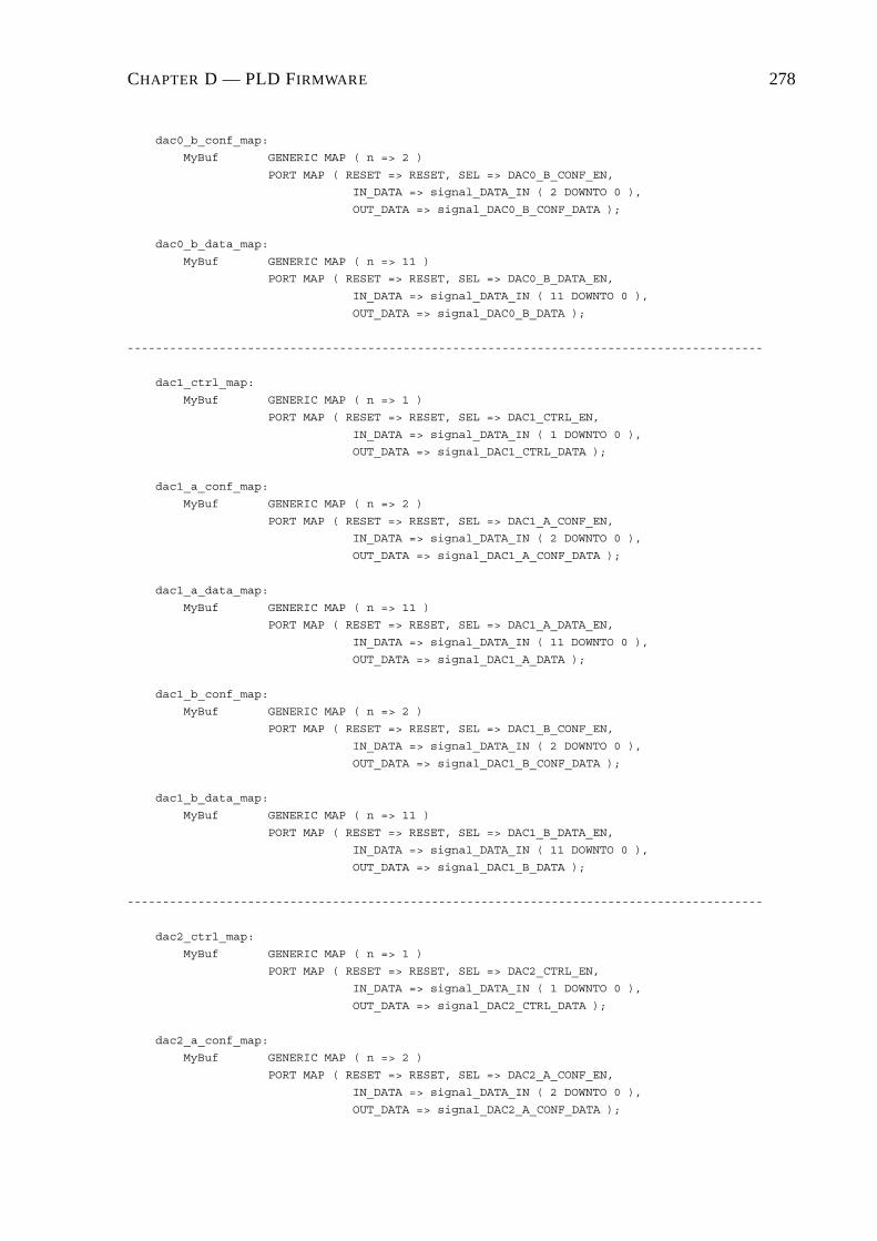
CHAPTER D — PLD FIRMWARE 278
dac0_b_conf_map:
MyBuf GENERIC MAP ( n => 2 )
PORT MAP ( RESET => RESET, SEL => DAC0_B_CONF_EN,
IN_DATA => signal_DATA_IN ( 2 DOWNTO 0 ),
OUT_DATA => signal_DAC0_B_CONF_DATA );
dac0_b_data_map:
MyBuf GENERIC MAP ( n => 11 )
PORT MAP ( RESET => RESET, SEL => DAC0_B_DATA_EN,
IN_DATA => signal_DATA_IN ( 11 DOWNTO 0 ),
OUT_DATA => signal_DAC0_B_DATA );
------------------------------------------------------------------------------------------
dac1_ctrl_map:
MyBuf GENERIC MAP ( n => 1 )
PORT MAP ( RESET => RESET, SEL => DAC1_CTRL_EN,
IN_DATA => signal_DATA_IN ( 1 DOWNTO 0 ),
OUT_DATA => signal_DAC1_CTRL_DATA );
dac1_a_conf_map:
MyBuf GENERIC MAP ( n => 2 )
PORT MAP ( RESET => RESET, SEL => DAC1_A_CONF_EN,
IN_DATA => signal_DATA_IN ( 2 DOWNTO 0 ),
OUT_DATA => signal_DAC1_A_CONF_DATA );
dac1_a_data_map:
MyBuf GENERIC MAP ( n => 11 )
PORT MAP ( RESET => RESET, SEL => DAC1_A_DATA_EN,
IN_DATA => signal_DATA_IN ( 11 DOWNTO 0 ),
OUT_DATA => signal_DAC1_A_DATA );
dac1_b_conf_map:
MyBuf GENERIC MAP ( n => 2 )
PORT MAP ( RESET => RESET, SEL => DAC1_B_CONF_EN,
IN_DATA => signal_DATA_IN ( 2 DOWNTO 0 ),
OUT_DATA => signal_DAC1_B_CONF_DATA );
dac1_b_data_map:
MyBuf GENERIC MAP ( n => 11 )
PORT MAP ( RESET => RESET, SEL => DAC1_B_DATA_EN,
IN_DATA => signal_DATA_IN ( 11 DOWNTO 0 ),
OUT_DATA => signal_DAC1_B_DATA );
------------------------------------------------------------------------------------------
dac2_ctrl_map:
MyBuf GENERIC MAP ( n => 1 )
PORT MAP ( RESET => RESET, SEL => DAC2_CTRL_EN,
IN_DATA => signal_DATA_IN ( 1 DOWNTO 0 ),
OUT_DATA => signal_DAC2_CTRL_DATA );
dac2_a_conf_map:
MyBuf GENERIC MAP ( n => 2 )
PORT MAP ( RESET => RESET, SEL => DAC2_A_CONF_EN,
IN_DATA => signal_DATA_IN ( 2 DOWNTO 0 ),
OUT_DATA => signal_DAC2_A_CONF_DATA );

CHAPTER D — PLD FIRMWARE 279
dac2_a_data_map:
MyBuf GENERIC MAP ( n => 11 )
PORT MAP ( RESET => RESET, SEL => DAC2_A_DATA_EN,
IN_DATA => signal_DATA_IN ( 11 DOWNTO 0 ),
OUT_DATA => signal_DAC2_A_DATA );
dac2_b_conf_map:
MyBuf GENERIC MAP ( n => 2 )
PORT MAP ( RESET => RESET, SEL => DAC2_B_CONF_EN,
IN_DATA => signal_DATA_IN ( 2 DOWNTO 0 ),
OUT_DATA => signal_DAC2_B_CONF_DATA );
dac2_b_data_map:
MyBuf GENERIC MAP ( n => 11 )
PORT MAP ( RESET => RESET, SEL => DAC2_B_DATA_EN,
IN_DATA => signal_DATA_IN ( 11 DOWNTO 0 ),
OUT_DATA => signal_DAC2_B_DATA );
------------------------------------------------------------------------------------------
dac3_ctrl_map:
MyBuf GENERIC MAP ( n => 1 )
PORT MAP ( RESET => RESET, SEL => DAC3_CTRL_EN,
IN_DATA => signal_DATA_IN ( 1 DOWNTO 0 ),
OUT_DATA => signal_DAC3_CTRL_DATA );
dac3_a_conf_map:
MyBuf GENERIC MAP ( n => 2 )
PORT MAP ( RESET => RESET, SEL => DAC3_A_CONF_EN,
IN_DATA => signal_DATA_IN ( 2 DOWNTO 0 ),
OUT_DATA => signal_DAC3_A_CONF_DATA );
dac3_a_data_map:
MyBuf GENERIC MAP ( n => 11 )
PORT MAP ( RESET => RESET, SEL => DAC3_A_DATA_EN,
IN_DATA => signal_DATA_IN ( 11 DOWNTO 0 ),
OUT_DATA => signal_DAC3_A_DATA );
dac3_b_conf_map:
MyBuf GENERIC MAP ( n => 2 )
PORT MAP ( RESET => RESET, SEL => DAC3_B_CONF_EN,
IN_DATA => signal_DATA_IN ( 2 DOWNTO 0 ),
OUT_DATA => signal_DAC3_B_CONF_DATA );
dac3_b_data_map:
MyBuf GENERIC MAP ( n => 11 )
PORT MAP ( RESET => RESET, SEL => DAC3_B_DATA_EN,
IN_DATA => signal_DATA_IN ( 11 DOWNTO 0 ),
OUT_DATA => signal_DAC3_B_DATA );
------------------------------------------------------------------------------------------
------------------------------------------------------------------------------------------
adc0_conf_map:
MyBuf GENERIC MAP ( n => 9 )
PORT MAP ( RESET => RESET, SEL => ADC0_CONF_EN,
IN_DATA => signal_DATA_IN ( 9 DOWNTO 0 ),
OUT_DATA => signal_ADC0_CONF_DATA );
adc0_samp_chan0_map:

CHAPTER D — PLD FIRMWARE 280
MyBuf GENERIC MAP ( n => 2 )
PORT MAP ( RESET => RESET, SEL => ADC0_SAMP_CHAN0_EN,
IN_DATA => signal_DATA_IN ( 2 DOWNTO 0 ),
OUT_DATA => signal_ADC0_SAMP_CHAN0 );
adc0_samp_chan1_map:
MyBuf GENERIC MAP ( n => 2 )
PORT MAP ( RESET => RESET, SEL => ADC0_SAMP_CHAN1_EN,
IN_DATA => signal_DATA_IN ( 2 DOWNTO 0 ),
OUT_DATA => signal_ADC0_SAMP_CHAN1 );
adc0_samp_chan2_map:
MyBuf GENERIC MAP ( n => 2 )
PORT MAP ( RESET => RESET, SEL => ADC0_SAMP_CHAN2_EN,
IN_DATA => signal_DATA_IN ( 2 DOWNTO 0 ),
OUT_DATA => signal_ADC0_SAMP_CHAN2 );
adc0_samp_chan3_map:
MyBuf GENERIC MAP ( n => 2 )
PORT MAP ( RESET => RESET, SEL => ADC0_SAMP_CHAN3_EN,
IN_DATA => signal_DATA_IN ( 2 DOWNTO 0 ),
OUT_DATA => signal_ADC0_SAMP_CHAN3 );
adc0_samp_chan4_map:
MyBuf GENERIC MAP ( n => 2 )
PORT MAP ( RESET => RESET, SEL => ADC0_SAMP_CHAN4_EN,
IN_DATA => signal_DATA_IN ( 2 DOWNTO 0 ),
OUT_DATA => signal_ADC0_SAMP_CHAN4 );
adc0_samp_chan5_map:
MyBuf GENERIC MAP ( n => 2 )
PORT MAP ( RESET => RESET, SEL => ADC0_SAMP_CHAN5_EN,
IN_DATA => signal_DATA_IN ( 2 DOWNTO 0 ),
OUT_DATA => signal_ADC0_SAMP_CHAN5 );
adc0_samp_chan6_map:
MyBuf GENERIC MAP ( n => 2 )
PORT MAP ( RESET => RESET, SEL => ADC0_SAMP_CHAN6_EN,
IN_DATA => signal_DATA_IN ( 2 DOWNTO 0 ),
OUT_DATA => signal_ADC0_SAMP_CHAN6 );
adc0_samp_chan7_map:
MyBuf GENERIC MAP ( n => 2 )
PORT MAP ( RESET => RESET, SEL => ADC0_SAMP_CHAN7_EN,
IN_DATA => signal_DATA_IN ( 2 DOWNTO 0 ),
OUT_DATA => signal_ADC0_SAMP_CHAN7 );
------------------------------------------------------------------------------------------
adc1_conf_map:
MyBuf GENERIC MAP ( n => 9 )
PORT MAP ( RESET => RESET, SEL => ADC1_CONF_EN,
IN_DATA => signal_DATA_IN ( 9 DOWNTO 0 ),
OUT_DATA => signal_ADC1_CONF_DATA );
adc1_samp_chan0_map:
MyBuf GENERIC MAP ( n => 2 )
PORT MAP ( RESET => RESET, SEL => ADC1_SAMP_CHAN0_EN,
IN_DATA => signal_DATA_IN ( 2 DOWNTO 0 ),
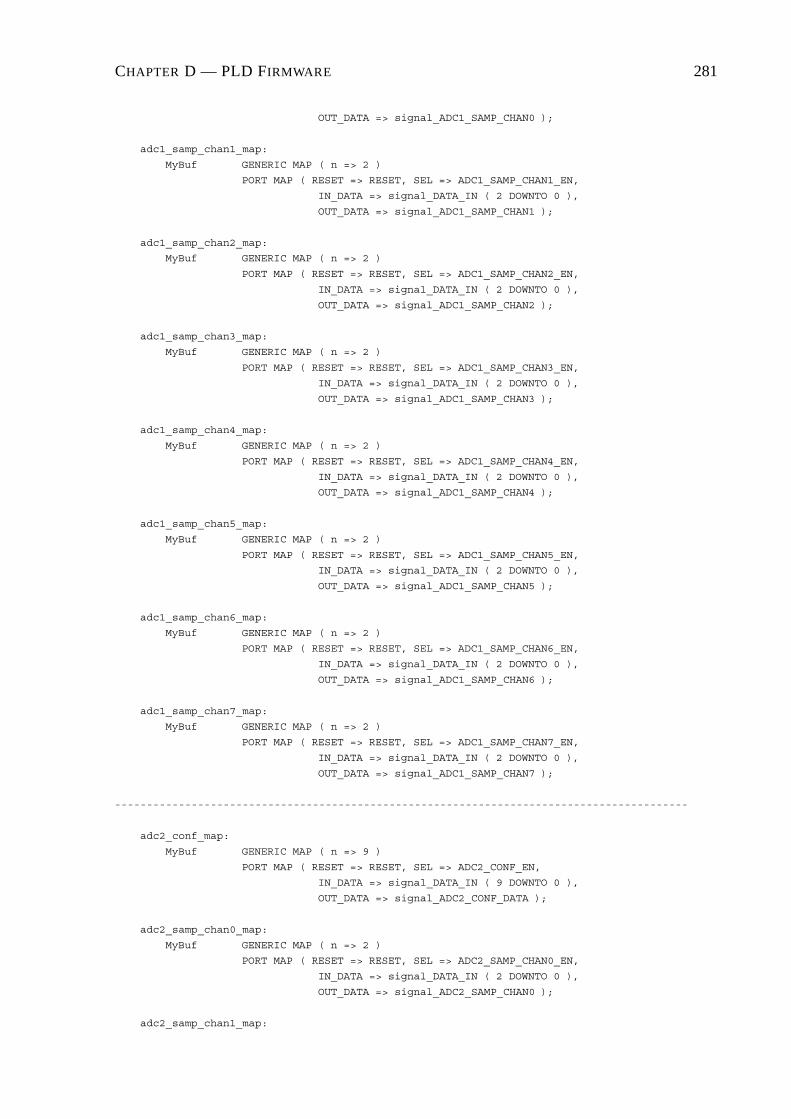
CHAPTER D — PLD FIRMWARE 281
OUT_DATA => signal_ADC1_SAMP_CHAN0 );
adc1_samp_chan1_map:
MyBuf GENERIC MAP ( n => 2 )
PORT MAP ( RESET => RESET, SEL => ADC1_SAMP_CHAN1_EN,
IN_DATA => signal_DATA_IN ( 2 DOWNTO 0 ),
OUT_DATA => signal_ADC1_SAMP_CHAN1 );
adc1_samp_chan2_map:
MyBuf GENERIC MAP ( n => 2 )
PORT MAP ( RESET => RESET, SEL => ADC1_SAMP_CHAN2_EN,
IN_DATA => signal_DATA_IN ( 2 DOWNTO 0 ),
OUT_DATA => signal_ADC1_SAMP_CHAN2 );
adc1_samp_chan3_map:
MyBuf GENERIC MAP ( n => 2 )
PORT MAP ( RESET => RESET, SEL => ADC1_SAMP_CHAN3_EN,
IN_DATA => signal_DATA_IN ( 2 DOWNTO 0 ),
OUT_DATA => signal_ADC1_SAMP_CHAN3 );
adc1_samp_chan4_map:
MyBuf GENERIC MAP ( n => 2 )
PORT MAP ( RESET => RESET, SEL => ADC1_SAMP_CHAN4_EN,
IN_DATA => signal_DATA_IN ( 2 DOWNTO 0 ),
OUT_DATA => signal_ADC1_SAMP_CHAN4 );
adc1_samp_chan5_map:
MyBuf GENERIC MAP ( n => 2 )
PORT MAP ( RESET => RESET, SEL => ADC1_SAMP_CHAN5_EN,
IN_DATA => signal_DATA_IN ( 2 DOWNTO 0 ),
OUT_DATA => signal_ADC1_SAMP_CHAN5 );
adc1_samp_chan6_map:
MyBuf GENERIC MAP ( n => 2 )
PORT MAP ( RESET => RESET, SEL => ADC1_SAMP_CHAN6_EN,
IN_DATA => signal_DATA_IN ( 2 DOWNTO 0 ),
OUT_DATA => signal_ADC1_SAMP_CHAN6 );
adc1_samp_chan7_map:
MyBuf GENERIC MAP ( n => 2 )
PORT MAP ( RESET => RESET, SEL => ADC1_SAMP_CHAN7_EN,
IN_DATA => signal_DATA_IN ( 2 DOWNTO 0 ),
OUT_DATA => signal_ADC1_SAMP_CHAN7 );
------------------------------------------------------------------------------------------
adc2_conf_map:
MyBuf GENERIC MAP ( n => 9 )
PORT MAP ( RESET => RESET, SEL => ADC2_CONF_EN,
IN_DATA => signal_DATA_IN ( 9 DOWNTO 0 ),
OUT_DATA => signal_ADC2_CONF_DATA );
adc2_samp_chan0_map:
MyBuf GENERIC MAP ( n => 2 )
PORT MAP ( RESET => RESET, SEL => ADC2_SAMP_CHAN0_EN,
IN_DATA => signal_DATA_IN ( 2 DOWNTO 0 ),
OUT_DATA => signal_ADC2_SAMP_CHAN0 );
adc2_samp_chan1_map:

CHAPTER D — PLD FIRMWARE 282
MyBuf GENERIC MAP ( n => 2 )
PORT MAP ( RESET => RESET, SEL => ADC2_SAMP_CHAN1_EN,
IN_DATA => signal_DATA_IN ( 2 DOWNTO 0 ),
OUT_DATA => signal_ADC2_SAMP_CHAN1 );
adc2_samp_chan2_map:
MyBuf GENERIC MAP ( n => 2 )
PORT MAP ( RESET => RESET, SEL => ADC2_SAMP_CHAN2_EN,
IN_DATA => signal_DATA_IN ( 2 DOWNTO 0 ),
OUT_DATA => signal_ADC2_SAMP_CHAN2 );
adc2_samp_chan3_map:
MyBuf GENERIC MAP ( n => 2 )
PORT MAP ( RESET => RESET, SEL => ADC2_SAMP_CHAN3_EN,
IN_DATA => signal_DATA_IN ( 2 DOWNTO 0 ),
OUT_DATA => signal_ADC2_SAMP_CHAN3 );
adc2_samp_chan4_map:
MyBuf GENERIC MAP ( n => 2 )
PORT MAP ( RESET => RESET, SEL => ADC2_SAMP_CHAN4_EN,
IN_DATA => signal_DATA_IN ( 2 DOWNTO 0 ),
OUT_DATA => signal_ADC2_SAMP_CHAN4 );
adc2_samp_chan5_map:
MyBuf GENERIC MAP ( n => 2 )
PORT MAP ( RESET => RESET, SEL => ADC2_SAMP_CHAN5_EN,
IN_DATA => signal_DATA_IN ( 2 DOWNTO 0 ),
OUT_DATA => signal_ADC2_SAMP_CHAN5 );
adc2_samp_chan6_map:
MyBuf GENERIC MAP ( n => 2 )
PORT MAP ( RESET => RESET, SEL => ADC2_SAMP_CHAN6_EN,
IN_DATA => signal_DATA_IN ( 2 DOWNTO 0 ),
OUT_DATA => signal_ADC2_SAMP_CHAN6 );
adc2_samp_chan7_map:
MyBuf GENERIC MAP ( n => 2 )
PORT MAP ( RESET => RESET, SEL => ADC2_SAMP_CHAN7_EN,
IN_DATA => signal_DATA_IN ( 2 DOWNTO 0 ),
OUT_DATA => signal_ADC2_SAMP_CHAN7 );
------------------------------------------------------------------------------------------
adc3_conf_map:
MyBuf GENERIC MAP ( n => 9 )
PORT MAP ( RESET => RESET, SEL => ADC3_CONF_EN,
IN_DATA => signal_DATA_IN ( 9 DOWNTO 0 ),
OUT_DATA => signal_ADC3_CONF_DATA );
adc3_samp_chan0_map:
MyBuf GENERIC MAP ( n => 2 )
PORT MAP ( RESET => RESET, SEL => ADC3_SAMP_CHAN0_EN,
IN_DATA => signal_DATA_IN ( 2 DOWNTO 0 ),
OUT_DATA => signal_ADC3_SAMP_CHAN0 );
adc3_samp_chan1_map:
MyBuf GENERIC MAP ( n => 2 )
PORT MAP ( RESET => RESET, SEL => ADC3_SAMP_CHAN1_EN,
IN_DATA => signal_DATA_IN ( 2 DOWNTO 0 ),

CHAPTER D — PLD FIRMWARE 283
OUT_DATA => signal_ADC3_SAMP_CHAN1 );
adc3_samp_chan2_map:
MyBuf GENERIC MAP ( n => 2 )
PORT MAP ( RESET => RESET, SEL => ADC3_SAMP_CHAN2_EN,
IN_DATA => signal_DATA_IN ( 2 DOWNTO 0 ),
OUT_DATA => signal_ADC3_SAMP_CHAN2 );
adc3_samp_chan3_map:
MyBuf GENERIC MAP ( n => 2 )
PORT MAP ( RESET => RESET, SEL => ADC3_SAMP_CHAN3_EN,
IN_DATA => signal_DATA_IN ( 2 DOWNTO 0 ),
OUT_DATA => signal_ADC3_SAMP_CHAN3 );
adc3_samp_chan4_map:
MyBuf GENERIC MAP ( n => 2 )
PORT MAP ( RESET => RESET, SEL => ADC3_SAMP_CHAN4_EN,
IN_DATA => signal_DATA_IN ( 2 DOWNTO 0 ),
OUT_DATA => signal_ADC3_SAMP_CHAN4 );
adc3_samp_chan5_map:
MyBuf GENERIC MAP ( n => 2 )
PORT MAP ( RESET => RESET, SEL => ADC3_SAMP_CHAN5_EN,
IN_DATA => signal_DATA_IN ( 2 DOWNTO 0 ),
OUT_DATA => signal_ADC3_SAMP_CHAN5 );
adc3_samp_chan6_map:
MyBuf GENERIC MAP ( n => 2 )
PORT MAP ( RESET => RESET, SEL => ADC3_SAMP_CHAN6_EN,
IN_DATA => signal_DATA_IN ( 2 DOWNTO 0 ),
OUT_DATA => signal_ADC3_SAMP_CHAN6 );
adc3_samp_chan7_map:
MyBuf GENERIC MAP ( n => 2 )
PORT MAP ( RESET => RESET, SEL => ADC3_SAMP_CHAN7_EN,
IN_DATA => signal_DATA_IN ( 2 DOWNTO 0 ),
OUT_DATA => signal_ADC3_SAMP_CHAN7 );
------------------------------------------------------------------------------------------
------------------------------------------------------------------------------------------
lcd_mode_map:
MyBuf GENERIC MAP ( n => 7 )
PORT MAP ( RESET => RESET, SEL => LCD_MODE_EN,
IN_DATA => signal_DATA_IN ( 7 DOWNTO 0 ),
OUT_DATA => signal_LCD_MODE_DATA );
lcd_addr_map:
MyBuf GENERIC MAP ( n => 6 )
PORT MAP ( RESET => RESET, SEL => LCD_ADDR_EN,
IN_DATA => signal_DATA_IN ( 6 DOWNTO 0 ),
OUT_DATA => signal_LCD_ADDR ( 6 DOWNTO 0 ) );
lcd_char_map:
MyBuf GENERIC MAP ( n => 7 )
PORT MAP ( RESET => RESET, SEL => LCD_CHAR_EN,
IN_DATA => signal_DATA_IN ( 7 DOWNTO 0 ),
OUT_DATA => signal_LCD_CHAR ( 7 DOWNTO 0 ) );
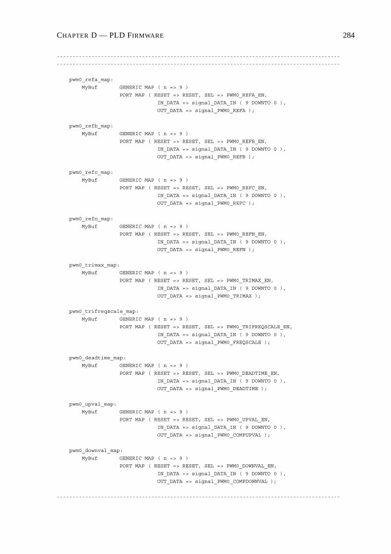
CHAPTER D — PLD FIRMWARE 284
------------------------------------------------------------------------------------------
------------------------------------------------------------------------------------------
pwm0_refa_map:
MyBuf GENERIC MAP ( n => 9 )
PORT MAP ( RESET => RESET, SEL => PWM0_REFA_EN,
IN_DATA => signal_DATA_IN ( 9 DOWNTO 0 ),
OUT_DATA => signal_PWM0_REFA );
pwm0_refb_map:
MyBuf GENERIC MAP ( n => 9 )
PORT MAP ( RESET => RESET, SEL => PWM0_REFB_EN,
IN_DATA => signal_DATA_IN ( 9 DOWNTO 0 ),
OUT_DATA => signal_PWM0_REFB );
pwm0_refc_map:
MyBuf GENERIC MAP ( n => 9 )
PORT MAP ( RESET => RESET, SEL => PWM0_REFC_EN,
IN_DATA => signal_DATA_IN ( 9 DOWNTO 0 ),
OUT_DATA => signal_PWM0_REFC );
pwm0_refn_map:
MyBuf GENERIC MAP ( n => 9 )
PORT MAP ( RESET => RESET, SEL => PWM0_REFN_EN,
IN_DATA => signal_DATA_IN ( 9 DOWNTO 0 ),
OUT_DATA => signal_PWM0_REFN );
pwm0_trimax_map:
MyBuf GENERIC MAP ( n => 9 )
PORT MAP ( RESET => RESET, SEL => PWM0_TRIMAX_EN,
IN_DATA => signal_DATA_IN ( 9 DOWNTO 0 ),
OUT_DATA => signal_PWM0_TRIMAX );
pwm0_trifreqscale_map:
MyBuf GENERIC MAP ( n => 9 )
PORT MAP ( RESET => RESET, SEL => PWM0_TRIFREQSCALE_EN,
IN_DATA => signal_DATA_IN ( 9 DOWNTO 0 ),
OUT_DATA => signal_PWM0_FREQSCALE );
pwm0_deadtime_map:
MyBuf GENERIC MAP ( n => 9 )
PORT MAP ( RESET => RESET, SEL => PWM0_DEADTIME_EN,
IN_DATA => signal_DATA_IN ( 9 DOWNTO 0 ),
OUT_DATA => signal_PWM0_DEADTIME );
pwm0_upval_map:
MyBuf GENERIC MAP ( n => 9 )
PORT MAP ( RESET => RESET, SEL => PWM0_UPVAL_EN,
IN_DATA => signal_DATA_IN ( 9 DOWNTO 0 ),
OUT_DATA => signal_PWM0_COMPUPVAL );
pwm0_downval_map:
MyBuf GENERIC MAP ( n => 9 )
PORT MAP ( RESET => RESET, SEL => PWM0_DOWNVAL_EN,
IN_DATA => signal_DATA_IN ( 9 DOWNTO 0 ),
OUT_DATA => signal_PWM0_COMPDOWNVAL );
------------------------------------------------------------------------------------------

CHAPTER D — PLD FIRMWARE 285
pwm1_refa_map:
MyBuf GENERIC MAP ( n => 9 )
PORT MAP ( RESET => RESET, SEL => PWM1_REFA_EN,
IN_DATA => signal_DATA_IN ( 9 DOWNTO 0 ),
OUT_DATA => signal_PWM1_REFA );
pwm1_refb_map:
MyBuf GENERIC MAP ( n => 9 )
PORT MAP ( RESET => RESET, SEL => PWM1_REFB_EN,
IN_DATA => signal_DATA_IN ( 9 DOWNTO 0 ),
OUT_DATA => signal_PWM1_REFB );
pwm1_refc_map:
MyBuf GENERIC MAP ( n => 9 )
PORT MAP ( RESET => RESET, SEL => PWM1_REFC_EN,
IN_DATA => signal_DATA_IN ( 9 DOWNTO 0 ),
OUT_DATA => signal_PWM1_REFC );
pwm1_refn_map:
MyBuf GENERIC MAP ( n => 9 )
PORT MAP ( RESET => RESET, SEL => PWM1_REFN_EN,
IN_DATA => signal_DATA_IN ( 9 DOWNTO 0 ),
OUT_DATA => signal_PWM1_REFN );
pwm1_trimax_map:
MyBuf GENERIC MAP ( n => 9 )
PORT MAP ( RESET => RESET, SEL => PWM1_TRIMAX_EN,
IN_DATA => signal_DATA_IN ( 9 DOWNTO 0 ),
OUT_DATA => signal_PWM1_TRIMAX );
pwm1_trifreqscale_map:
MyBuf GENERIC MAP ( n => 9 )
PORT MAP ( RESET => RESET, SEL => PWM1_TRIFREQSCALE_EN,
IN_DATA => signal_DATA_IN ( 9 DOWNTO 0 ),
OUT_DATA => signal_PWM1_FREQSCALE );
pwm1_deadtime_map:
MyBuf GENERIC MAP ( n => 9 )
PORT MAP ( RESET => RESET, SEL => PWM1_DEADTIME_EN,
IN_DATA => signal_DATA_IN ( 9 DOWNTO 0 ),
OUT_DATA => signal_PWM1_DEADTIME );
pwm1_upval_map:
MyBuf GENERIC MAP ( n => 9 )
PORT MAP ( RESET => RESET, SEL => PWM1_UPVAL_EN,
IN_DATA => signal_DATA_IN ( 9 DOWNTO 0 ),
OUT_DATA => signal_PWM1_COMPUPVAL );
pwm1_downval_map:
MyBuf GENERIC MAP ( n => 9 )
PORT MAP ( RESET => RESET, SEL => PWM1_DOWNVAL_EN,
IN_DATA => signal_DATA_IN ( 9 DOWNTO 0 ),
OUT_DATA => signal_PWM1_COMPDOWNVAL );
------------------------------------------------------------------------------------------
------------------------------------------------------------------------------------------
int_en_map:
MyBuf GENERIC MAP ( n => 14 )

CHAPTER D — PLD FIRMWARE 286
PORT MAP ( RESET => RESET, SEL => INT_EN_EN,
IN_DATA => signal_DATA_IN ( 14 DOWNTO 0 ),
OUT_DATA => signal_INT_EN );
------------------------------------------------------------------------------------------
------------------------------------------------------------------------------------------
cmd_reg0_map:
MyBuf GENERIC MAP ( n => 6 )
PORT MAP ( RESET => RESET, SEL => CMD_REG0_EN,
IN_DATA => signal_DATA_IN ( 6 DOWNTO 0 ),
OUT_DATA => signal_CMD_REG0 );
cmd_reg1_map:
MyBuf GENERIC MAP ( n => 5 )
PORT MAP ( RESET => RESET, SEL => CMD_REG1_EN,
IN_DATA => signal_DATA_IN ( 5 DOWNTO 0 ),
OUT_DATA => signal_CMD_REG1 );
------------------------------------------------------------------------------------------
------------------------------------------------------------------------------------------
bidir_bus_map:
bidir PORT MAP ( BIDIR => DATA, RnW => signal_RnW, CLK => CLK,
IN_DATA => signal_DATA_OUT, OUT_DATA => signal_DATA_IN );
------------------------------------------------------------------------------------------
------------------------------------------------------------------------------------------
signal_RnW
<= ’0’ WHEN ( ADC_STATUS_EN = ’1’ )or( ADC0_DATA_EN = ’1’ )or
( ADC1_DATA_EN = ’1’ )or( ADC2_DATA_EN = ’1’ )or
( ADC3_DATA_EN = ’1’ )or( KEYVAL_EN = ’1’ )or
( PWM_ERR_TOP_EN = ’1’ )or( PWM_ERR_BOT_EN = ’1’ )or
( LCD_STATUS_EN = ’1’ )or( PWM_STATUS_EN = ’1’ )or
( INT_REG_EN = ’1’) ELSE
’1’;
RnW
<= signal_RnW;
signal_DATA_OUT( 0 )
<= signal_ADC_STATUS ( 0 ) WHEN ( ADC_STATUS_EN = ’1’ ) ELSE
signal_ADC0_DATA ( 0 ) WHEN ( ADC0_DATA_EN = ’1’ ) ELSE
signal_ADC1_DATA ( 0 ) WHEN ( ADC1_DATA_EN = ’1’ ) ELSE
signal_ADC2_DATA ( 0 ) WHEN ( ADC2_DATA_EN = ’1’ ) ELSE
signal_ADC3_DATA ( 0 ) WHEN ( ADC3_DATA_EN = ’1’ ) ELSE
signal_LCD_STATUS WHEN ( LCD_STATUS_EN = ’1’ ) ELSE
signal_KEYVAL ( 0 ) WHEN ( KEYVAL_EN = ’1’ ) ELSE
signal_PWM_STATUS ( 0 ) WHEN ( PWM_STATUS_EN = ’1’ ) ELSE
signal_PWM_ERR_TOP ( 0 ) WHEN ( PWM_ERR_TOP_EN = ’1’ ) ELSE
signal_PWM_ERR_BOT ( 0 ) WHEN ( PWM_ERR_BOT_EN = ’1’ ) ELSE
signal_INT_REG ( 0 ) WHEN ( INT_REG_EN = ’1’ ) ELSE
’0’;
signal_DATA_OUT( 3 DOWNTO 1 )
<= signal_ADC_STATUS ( 3 DOWNTO 1 ) WHEN ( ADC_STATUS_EN = ’1’ ) ELSE
signal_ADC0_DATA ( 3 DOWNTO 1 ) WHEN ( ADC0_DATA_EN = ’1’ ) ELSE

CHAPTER D — PLD FIRMWARE 287
signal_ADC1_DATA ( 3 DOWNTO 1 ) WHEN ( ADC1_DATA_EN = ’1’ ) ELSE
signal_ADC2_DATA ( 3 DOWNTO 1 ) WHEN ( ADC2_DATA_EN = ’1’ ) ELSE
signal_ADC3_DATA ( 3 DOWNTO 1 ) WHEN ( ADC3_DATA_EN = ’1’ ) ELSE
signal_KEYVAL ( 3 DOWNTO 1 ) WHEN ( KEYVAL_EN = ’1’ ) ELSE
signal_PWM_STATUS ( 3 DOWNTO 1 ) WHEN ( PWM_STATUS_EN = ’1’ ) ELSE
signal_PWM_ERR_TOP ( 3 DOWNTO 1 ) WHEN ( PWM_ERR_TOP_EN = ’1’ ) ELSE
signal_PWM_ERR_BOT ( 3 DOWNTO 1 ) WHEN ( PWM_ERR_BOT_EN = ’1’ ) ELSE
signal_INT_REG ( 3 DOWNTO 1 ) WHEN ( INT_REG_EN = ’1’ ) ELSE
"000";
signal_DATA_OUT( 5 DOWNTO 4 )
<= signal_ADC0_DATA ( 5 DOWNTO 4 ) WHEN ( ADC0_DATA_EN = ’1’ ) ELSE
signal_ADC1_DATA ( 5 DOWNTO 4 ) WHEN ( ADC1_DATA_EN = ’1’ ) ELSE
signal_ADC2_DATA ( 5 DOWNTO 4 ) WHEN ( ADC2_DATA_EN = ’1’ ) ELSE
signal_ADC3_DATA ( 5 DOWNTO 4 ) WHEN ( ADC3_DATA_EN = ’1’ ) ELSE
signal_PWM_STATUS ( 5 DOWNTO 4 ) WHEN ( PWM_STATUS_EN = ’1’ ) ELSE
signal_PWM_ERR_TOP ( 5 DOWNTO 4 ) WHEN ( PWM_ERR_TOP_EN = ’1’ ) ELSE
signal_PWM_ERR_BOT ( 5 DOWNTO 4 ) WHEN ( PWM_ERR_BOT_EN = ’1’ ) ELSE
signal_INT_REG ( 5 DOWNTO 4 ) WHEN ( INT_REG_EN = ’1’ ) ELSE
"00";
signal_DATA_OUT( 7 DOWNTO 6 )
<= signal_ADC0_DATA ( 7 DOWNTO 6 ) WHEN ( ADC0_DATA_EN = ’1’ ) ELSE
signal_ADC1_DATA ( 7 DOWNTO 6 ) WHEN ( ADC1_DATA_EN = ’1’ ) ELSE
signal_ADC2_DATA ( 7 DOWNTO 6 ) WHEN ( ADC2_DATA_EN = ’1’ ) ELSE
signal_ADC3_DATA ( 7 DOWNTO 6 ) WHEN ( ADC3_DATA_EN = ’1’ ) ELSE
signal_PWM_STATUS ( 7 DOWNTO 6 ) WHEN ( PWM_STATUS_EN = ’1’ ) ELSE
signal_PWM_ERR_TOP ( 7 DOWNTO 6 ) WHEN ( PWM_ERR_TOP_EN = ’1’ ) ELSE
signal_PWM_ERR_BOT ( 7 DOWNTO 6 ) WHEN ( PWM_ERR_BOT_EN = ’1’ ) ELSE
"00";
signal_DATA_OUT( 8 )
<= signal_ADC0_DATA ( 8 ) WHEN ( ADC0_DATA_EN = ’1’ ) ELSE
signal_ADC1_DATA ( 8 ) WHEN ( ADC1_DATA_EN = ’1’ ) ELSE
signal_ADC2_DATA ( 8 ) WHEN ( ADC2_DATA_EN = ’1’ ) ELSE
signal_ADC3_DATA ( 8 ) WHEN ( ADC3_DATA_EN = ’1’ ) ELSE
signal_PWM_ERR_TOP ( 8 ) WHEN ( PWM_ERR_TOP_EN = ’1’ ) ELSE
signal_PWM_ERR_BOT ( 8 ) WHEN ( PWM_ERR_BOT_EN = ’1’ ) ELSE
’0’;
signal_DATA_OUT( 12 DOWNTO 9 )
<= signal_ADC0_DATA ( 12 DOWNTO 9 ) WHEN ( ADC0_DATA_EN = ’1’ ) ELSE
signal_ADC1_DATA ( 12 DOWNTO 9 ) WHEN ( ADC1_DATA_EN = ’1’ ) ELSE
signal_ADC2_DATA ( 12 DOWNTO 9 ) WHEN ( ADC2_DATA_EN = ’1’ ) ELSE
signal_ADC3_DATA ( 12 DOWNTO 9 ) WHEN ( ADC3_DATA_EN = ’1’ ) ELSE
"0000";
signal_DATA_OUT( 15 DOWNTO 13 ) <= "000";
END a;

CHAPTER D — PLD FIRMWARE 288
D.2.6 VHDL Code for the MyBuf Module of FPGA Analog-- PEC33 - Buffer 2002-10-28
LIBRARY ieee;
USE ieee.std_logic_1164.all;
USE ieee.std_logic_arith.all;
-- -------------------------------------------------------
-- | RESET | SEL | IN_DATA | OUT_DATA |
-- -------------------------------------------------------
-- -------------------------------------------------------
-- | 1 | X | XX...X | 00...0 |
-- -------------------------------------------------------
-- | 0 | 1 | Data | IN_DATA |
-- -------------------------------------------------------
-- | 0 | 0 | XX...X | OUT_DATA |
-- -------------------------------------------------------
ENTITY mybuf IS
GENERIC (
n : INTEGER RANGE 0 TO 15 := 15
);
PORT (
RESET : IN STD_LOGIC;
SEL : IN STD_LOGIC;
IN_DATA : IN STD_LOGIC_VECTOR ( n DOWNTO 0 );
OUT_DATA : OUT STD_LOGIC_VECTOR ( n DOWNTO 0 )
);
END mybuf;
ARCHITECTURE a OF mybuf IS
SIGNAL signal_out : STD_LOGIC_VECTOR ( n DOWNTO 0 );
BEGIN
signal_out <= ( OTHERS => ’0’ ) WHEN ( RESET = ’1’ ) ELSE
IN_DATA WHEN ( SEL = ’1’ ) ELSE
signal_out;
OUT_DATA <= signal_out;
END a;

CHAPTER D — PLD FIRMWARE 289
D.2.7 VHDL Code for the BiDir Module of FPGA Analog-- Bidirectional Bus 2002-11-07
LIBRARY ieee;
USE ieee.std_logic_1164.all;
USE ieee.std_logic_arith.all;
-- -------------------------------------------------------------------
-- | RnW | BIDIR | IN_DATA | OUT_DATA |
-- -------------------------------------------------------------------
-- -------------------------------------------------------------------
-- | 1 | ZZZZZZZZZZZZZZZZ | XXXXXXXXXXXXXXXX | BIDIR |
-- -------------------------------------------------------------------
-- | 0 | IN_DATA | Data | BIDIR |
-- -------------------------------------------------------------------
ENTITY Bidir IS
GENERIC (
n : INTEGER RANGE 0 TO 31 := 15
);
PORT (
BIDIR : INOUT STD_LOGIC_VECTOR ( n DOWNTO 0 );
RnW : IN STD_LOGIC;
CLK : IN STD_LOGIC;
IN_DATA : IN STD_LOGIC_VECTOR ( n DOWNTO 0 );
OUT_DATA : OUT STD_LOGIC_VECTOR ( n DOWNTO 0 )
);
END Bidir;
ARCHITECTURE maxpld OF Bidir IS
SIGNAL a : STD_LOGIC_VECTOR ( n DOWNTO 0 );
SIGNAL b : STD_LOGIC_VECTOR ( n DOWNTO 0 );
BEGIN
PROCESS ( CLK )
BEGIN
IF ( CLK’event )and( CLK = ’0’ ) THEN
a <= IN_DATA;
OUT_DATA <= b;
END IF;
END PROCESS;
PROCESS ( RnW, BIDIR )
BEGIN
IF ( RnW = ’1’ ) THEN
BIDIR <= ( others => ’Z’ );
b <= BIDIR;
ELSE
BIDIR <= a;

CHAPTER D — PLD FIRMWARE 290
b <= BIDIR;
END IF;
END PROCESS;
END maxpld;
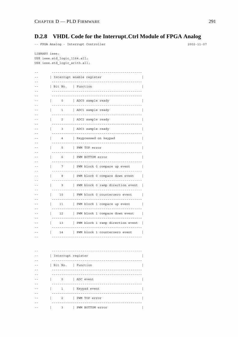
CHAPTER D — PLD FIRMWARE 291
D.2.8 VHDL Code for the Interrupt Ctrl Module of FPGA Analog-- FPGA Analog - Interrupt Controller 2002-11-07
LIBRARY ieee;
USE ieee.std_logic_1164.all;
USE ieee.std_logic_arith.all;
-- -----------------------------------------------
-- | Interrupt enable register |
-- -----------------------------------------------
-- | Bit No. | Function |
-- -----------------------------------------------
-- -----------------------------------------------
-- | 0 | ADC0 sample ready |
-- -----------------------------------------------
-- | 1 | ADC1 sample ready |
-- -----------------------------------------------
-- | 2 | ADC2 sample ready |
-- -----------------------------------------------
-- | 3 | ADC3 sample ready |
-- -----------------------------------------------
-- | 4 | Keypressed on keypad |
-- -----------------------------------------------
-- | 5 | PWM TOP error |
-- -----------------------------------------------
-- | 6 | PWM BOTTOM error |
-- -----------------------------------------------
-- | 7 | PWM block 0 compare up event |
-- -----------------------------------------------
-- | 8 | PWM block 0 compare down event |
-- -----------------------------------------------
-- | 9 | PWM block 0 ramp direction event |
-- -----------------------------------------------
-- | 10 | PWM block 0 counterzero event |
-- -----------------------------------------------
-- | 11 | PWM block 1 compare up event |
-- -----------------------------------------------
-- | 12 | PWM block 1 compare down event |
-- -----------------------------------------------
-- | 13 | PWM block 1 ramp direction event |
-- -----------------------------------------------
-- | 14 | PWM block 1 counterzero event |
-- -----------------------------------------------
-- -----------------------------------------------
-- | Interrupt register |
-- -----------------------------------------------
-- | Bit No. | Function |
-- -----------------------------------------------
-- -----------------------------------------------
-- | 0 | ADC event |
-- -----------------------------------------------
-- | 1 | Keypad event |
-- -----------------------------------------------
-- | 2 | PWM TOP error |
-- -----------------------------------------------
-- | 3 | PWM BOTTOM error |

CHAPTER D — PLD FIRMWARE 292
-- -----------------------------------------------
-- | 4 | PWM block 0 event |
-- -----------------------------------------------
-- | 5 | PWM block 1 event |
-- -----------------------------------------------
ENTITY INTERRUPT_CTRL IS
PORT (
ADC_STATUS_IN : IN STD_LOGIC_VECTOR ( 3 DOWNTO 0 );
ADC_STATUS_OUT : OUT STD_LOGIC_VECTOR ( 3 DOWNTO 0 );
KEYPAD_IN : IN STD_LOGIC_VECTOR ( 3 DOWNTO 0 );
KEYPAD_OUT : OUT STD_LOGIC_VECTOR ( 3 DOWNTO 0 );
PWM_ERROR_TOP_IN : IN STD_LOGIC_VECTOR ( 8 DOWNTO 0 );
PWM_ERROR_TOP_OUT : OUT STD_LOGIC_VECTOR ( 8 DOWNTO 0 );
PWM_ERROR_BOT_IN : IN STD_LOGIC_VECTOR ( 8 DOWNTO 0 );
PWM_ERROR_BOT_OUT : OUT STD_LOGIC_VECTOR ( 8 DOWNTO 0 );
PWM0_COMPUP : IN STD_LOGIC;
PWM0_COMPDOWN : IN STD_LOGIC;
PWM0_RAMPDIR : IN STD_LOGIC;
PWM0_COUNTERZERO : IN STD_LOGIC;
PWM1_COMPUP : IN STD_LOGIC;
PWM1_COMPDOWN : IN STD_LOGIC;
PWM1_RAMPDIR : IN STD_LOGIC;
PWM1_COUNTERZERO : IN STD_LOGIC;
PWM_STATUS_OUT : OUT STD_LOGIC_VECTOR ( 7 DOWNTO 0 );
INT_EN_IN : IN STD_LOGIC_VECTOR ( 14 DOWNTO 0 );
INT_REG : OUT STD_LOGIC_VECTOR ( 5 DOWNTO 0 );
INT0_OUT : OUT STD_LOGIC;
INT2_OUT : OUT STD_LOGIC;
RESET : IN STD_LOGIC;
CLK : IN STD_LOGIC -- Input clock is 30MHz
);
END INTERRUPT_CTRL;
ARCHITECTURE a OF INTERRUPT_CTRL IS
SIGNAL prev_adc_status : STD_LOGIC_VECTOR ( 3 DOWNTO 0 );
SIGNAL signal_adc_status_out : STD_LOGIC_VECTOR ( 3 DOWNTO 0 );
SIGNAL adc_int : STD_LOGIC;
SIGNAL prev_keypad_value : STD_LOGIC_VECTOR ( 3 DOWNTO 0 );
SIGNAL keypad_int : STD_LOGIC;
SIGNAL prev_error_top_status : STD_LOGIC_VECTOR ( 8 DOWNTO 0 );
SIGNAL signal_error_top_status_out : STD_LOGIC_VECTOR ( 8 DOWNTO 0 );
SIGNAL error_top_int : STD_LOGIC;
CHAPTER D — PLD FIRMWARE 293
SIGNAL prev_error_bot_status : STD_LOGIC_VECTOR ( 8 DOWNTO 0 );
SIGNAL signal_error_bot_status_out : STD_LOGIC_VECTOR ( 8 DOWNTO 0 );
SIGNAL error_bot_int : STD_LOGIC;
SIGNAL pwm0_status_in : STD_LOGIC_VECTOR ( 3 DOWNTO 0 );
SIGNAL prev_pwm0_status : STD_LOGIC_VECTOR ( 3 DOWNTO 0 );
SIGNAL signal_pwm0_status_out : STD_LOGIC_VECTOR ( 3 DOWNTO 0 );
SIGNAL pwm0_status_int : STD_LOGIC;
SIGNAL pwm1_status_in : STD_LOGIC_VECTOR ( 3 DOWNTO 0 );
SIGNAL prev_pwm1_status : STD_LOGIC_VECTOR ( 3 DOWNTO 0 );
SIGNAL signal_pwm1_status_out : STD_LOGIC_VECTOR ( 3 DOWNTO 0 );
SIGNAL pwm1_status_int : STD_LOGIC;
SIGNAL int0_trig : STD_LOGIC;
SIGNAL int2_trig : STD_LOGIC;
SIGNAL int0_cntr : INTEGER RANGE 0 TO 7;
SIGNAL int2_cntr : INTEGER RANGE 0 TO 7;
SIGNAL signal_INT_REG : STD_LOGIC_VECTOR ( 5 DOWNTO 0 );
SIGNAL signal_prev_INT_REG : STD_LOGIC_VECTOR ( 5 DOWNTO 0 );
BEGIN
int0_trig <= ( adc_int )and( keypad_int )and
( pwm0_status_int )and( pwm1_status_int );
int2_trig <= ( error_top_int )and( error_bot_int );
INT_REG <= signal_INT_REG;
ADC_STATUS_OUT <= not signal_adc_status_out;
signal_INT_REG( 0 ) <= ’0’ WHEN ( INT_EN_IN( 3 DOWNTO 0 ) = "0000" ) ELSE
’1’ WHEN ( signal_adc_status_out /= "1111" ) ELSE
’0’;
KEYPAD_OUT <= prev_keypad_value;
PWM_ERROR_TOP_OUT <= not signal_error_top_status_out;
PWM_ERROR_BOT_OUT <= not signal_error_bot_status_out;
pwm0_status_in( 0 ) <= PWM0_COMPUP;
pwm0_status_in( 1 ) <= PWM0_COMPDOWN;
pwm0_status_in( 2 ) <= PWM0_RAMPDIR;
pwm0_status_in( 3 ) <= PWM0_COUNTERZERO;
pwm1_status_in( 0 ) <= PWM1_COMPUP;
pwm1_status_in( 1 ) <= PWM1_COMPDOWN;
pwm1_status_in( 2 ) <= PWM1_RAMPDIR;
pwm1_status_in( 3 ) <= PWM1_COUNTERZERO;
PWM_STATUS_OUT ( 3 DOWNTO 0 )
<= signal_pwm0_status_out;
signal_INT_REG( 4 ) <= ’0’ WHEN ( INT_EN_IN( 10 DOWNTO 7 ) = "0000" ) ELSE
’1’ WHEN ( signal_pwm0_status_out /= "0000" ) ELSE
’0’;
PWM_STATUS_OUT ( 7 DOWNTO 4 )

CHAPTER D — PLD FIRMWARE 294
<= signal_pwm1_status_out;
signal_INT_REG( 5 ) <= ’0’ WHEN ( INT_EN_IN( 14 DOWNTO 11 ) = "0000" ) ELSE
’1’ WHEN ( signal_pwm1_status_out /= "0000" ) ELSE
’0’;
------------------------------------------------------------------------------------------
int0_proc:
PROCESS ( CLK, int0_trig )
BEGIN
IF ( int0_trig = ’0’ ) THEN
INT0_OUT <= ’1’;
int0_cntr <= 0;
ELSIF ( CLK’event )and( CLK = ’1’ ) THEN
IF ( RESET = ’1’ )or( int0_cntr = 7 ) THEN
int0_cntr <= 7;
INT0_OUT <= ’1’;
ELSE
int0_cntr <= int0_cntr+1;
INT0_OUT <= ’0’;
END IF;
END IF;
END PROCESS int0_proc;
------------------------------------------------------------------------------------------
int2_proc:
PROCESS ( CLK, int2_trig )
BEGIN
IF ( int2_trig = ’0’ ) THEN
INT2_OUT <= ’1’;
int2_cntr <= 0;
ELSIF ( CLK’event )and( CLK = ’1’ ) THEN
IF ( RESET = ’1’ )or( int2_cntr = 7 ) THEN
int2_cntr <= 7;
INT2_OUT <= ’1’;
ELSE
int2_cntr <= int2_cntr+1;
INT2_OUT <= ’0’;
END IF;
END IF;
END PROCESS int2_proc;
------------------------------------------------------------------------------------------
adc_status_proc:
PROCESS ( CLK, RESET )

CHAPTER D — PLD FIRMWARE 295
BEGIN
IF ( RESET = ’1’ ) THEN
adc_int <= ’1’;
prev_adc_status <= "1111";
signal_adc_status_out <= "1111";
ELSIF ( CLK’event )and( CLK = ’1’ ) THEN
IF ( ( (not ADC_STATUS_IN)and
(INT_EN_IN( 3 DOWNTO 0 )) ) = "0000" ) THEN
adc_int <= ’1’;
prev_adc_status <= ADC_STATUS_IN;
signal_adc_status_out <= signal_adc_status_out;
ELSIF ( ADC_STATUS_IN /= prev_adc_status ) THEN
adc_int <= ’0’;
prev_adc_status <= ADC_STATUS_IN;
signal_adc_status_out <= ADC_STATUS_IN;
ELSE
adc_int <= ’1’;
prev_adc_status <= prev_adc_status;
signal_adc_status_out <= signal_adc_status_out;
END IF;
END IF;
END PROCESS adc_status_proc;
------------------------------------------------------------------------------------------
keypad_proc:
PROCESS ( CLK, RESET )
BEGIN
IF ( RESET = ’1’ ) THEN
keypad_int <= ’1’;
signal_INT_REG( 1 ) <= ’0’;
prev_keypad_value <= "0000";
ELSIF ( CLK’event )and( CLK = ’1’ ) THEN
IF ( INT_EN_IN( 4 ) = ’0’ ) THEN
keypad_int <= ’1’;
signal_INT_REG( 1 ) <= ’0’;
prev_keypad_value <= prev_keypad_value;
ELSIF ( KEYPAD_IN /= prev_keypad_value ) THEN
keypad_int <= ’0’;
signal_INT_REG( 1 ) <= ’1’;
prev_keypad_value <= KEYPAD_IN;
ELSE
keypad_int <= ’1’;
signal_INT_REG( 1 ) <= signal_INT_REG( 1 );
prev_keypad_value <= prev_keypad_value;
END IF;
END IF;
END PROCESS keypad_proc;
CHAPTER D — PLD FIRMWARE 296
------------------------------------------------------------------------------------------
pwm_error_top_proc:
PROCESS ( CLK, RESET )
BEGIN
IF ( RESET = ’1’ ) THEN
error_top_int <= ’1’;
signal_INT_REG( 2 ) <= ’0’;
prev_error_top_status <= "111111111";
signal_error_top_status_out <= "111111111";
ELSIF ( CLK’event )and( CLK = ’1’ ) THEN
IF ( ( (not PWM_ERROR_TOP_IN) = "000000000" )or
( INT_EN_IN( 5 ) = ’0’) ) THEN
error_top_int <= ’1’;
signal_INT_REG( 2 ) <= ’0’;
prev_error_top_status <= PWM_ERROR_TOP_IN;
signal_error_top_status_out <= signal_error_top_status_out;
ELSIF ( PWM_ERROR_TOP_IN /= prev_error_top_status ) THEN
error_top_int <= ’0’;
signal_INT_REG( 2 ) <= ’1’;
prev_error_top_status <= PWM_ERROR_TOP_IN;
signal_error_top_status_out <= PWM_ERROR_TOP_IN;
ELSE
error_top_int <= ’1’;
signal_INT_REG( 2 ) <= signal_INT_REG( 2 );
prev_error_top_status <= prev_error_top_status;
signal_error_top_status_out <= signal_error_top_status_out;
END IF;
END IF;
END PROCESS pwm_error_top_proc;
------------------------------------------------------------------------------------------
pwm_error_bot_proc:
PROCESS ( CLK, RESET )
BEGIN
IF ( RESET = ’1’ ) THEN
error_bot_int <= ’1’;
signal_INT_REG( 3 ) <= ’0’;
prev_error_bot_status <= "111111111";
signal_error_bot_status_out <= "111111111";
ELSIF ( CLK’event )and( CLK = ’1’ ) THEN
IF ( ( (not PWM_ERROR_BOT_IN) = "000000000" )or
( INT_EN_IN( 6 ) = ’0’) ) THEN
error_bot_int <= ’1’;
signal_INT_REG( 3 ) <= ’0’;
prev_error_bot_status <= PWM_ERROR_BOT_IN;
signal_error_bot_status_out <= signal_error_bot_status_out;

CHAPTER D — PLD FIRMWARE 297
ELSIF ( PWM_ERROR_BOT_IN /= prev_error_bot_status ) THEN
error_bot_int <= ’0’;
signal_INT_REG( 3 ) <= ’1’;
prev_error_bot_status <= PWM_ERROR_BOT_IN;
signal_error_bot_status_out <= PWM_ERROR_BOT_IN;
ELSE
error_bot_int <= ’1’;
signal_INT_REG( 3 ) <= signal_INT_REG( 3 );
prev_error_bot_status <= prev_error_bot_status;
signal_error_bot_status_out <= signal_error_bot_status_out;
END IF;
END IF;
END PROCESS pwm_error_bot_proc;
------------------------------------------------------------------------------------------
pwm0_status_proc:
PROCESS ( CLK, RESET )
BEGIN
IF ( RESET = ’1’ ) THEN
pwm0_status_int <= ’1’;
prev_pwm0_status <= "0000";
signal_pwm0_status_out <= "0000";
ELSIF ( CLK’event )and( CLK = ’1’ ) THEN
IF ( ( (pwm0_status_in)and(INT_EN_IN( 10 DOWNTO 7 )) ) = "0000" ) THEN
pwm0_status_int <= ’1’;
prev_pwm0_status <= pwm0_status_in;
signal_pwm0_status_out <= signal_pwm0_status_out;
ELSIF ( pwm0_status_in /= prev_pwm0_status ) THEN
pwm0_status_int <= ’0’;
prev_pwm0_status <= pwm0_status_in;
signal_pwm0_status_out <= pwm0_status_in;
ELSE
pwm0_status_int <= ’1’;
prev_pwm0_status <= prev_pwm0_status;
signal_pwm0_status_out <= signal_pwm0_status_out;
END IF;
END IF;
END PROCESS pwm0_status_proc;
------------------------------------------------------------------------------------------
pwm1_status_proc:
PROCESS ( CLK, RESET )
BEGIN
IF ( RESET = ’1’ ) THEN
pwm1_status_int <= ’1’;
prev_pwm1_status <= "0000";

CHAPTER D — PLD FIRMWARE 298
signal_pwm1_status_out <= "0000";
ELSIF ( CLK’event )and( CLK = ’1’ ) THEN
IF ( ( (pwm1_status_in)and(INT_EN_IN( 14 DOWNTO 11 )) ) = "0000" ) THEN
pwm1_status_int <= ’1’;
prev_pwm1_status <= pwm1_status_in;
signal_pwm1_status_out <= signal_pwm1_status_out;
ELSIF ( pwm1_status_in /= prev_pwm1_status ) THEN
pwm1_status_int <= ’0’;
prev_pwm1_status <= pwm1_status_in;
signal_pwm1_status_out <= pwm1_status_in;
ELSE
pwm1_status_int <= ’1’;
prev_pwm1_status <= prev_pwm1_status;
signal_pwm1_status_out <= signal_pwm1_status_out;
END IF;
END IF;
END PROCESS pwm1_status_proc;
END a;

CHAPTER D — PLD FIRMWARE 299
D.2.9 VHDL Code for the ADC Ctrl Module of FPGA Analog-- FPGA Analog - ADC_Ctrl 2002-11-07
LIBRARY ieee;
USE ieee.std_logic_1164.all;
USE ieee.std_logic_arith.all;
ENTITY ADC_CTRL IS
PORT (
ADC_SDOUT : IN STD_LOGIC; -- ADC serial data output
ADC_SDIN : OUT STD_LOGIC; -- ADC serial data input
ADC_nCS : OUT STD_LOGIC; -- ADC not chip select input
ADC_SCLK : OUT STD_LOGIC; -- ADC clock is 15MHz
ADC_DATA : OUT STD_LOGIC_VECTOR ( 9 DOWNTO 0 ); -- Previous sample
ADC_DATA_RDY : OUT STD_LOGIC; -- New sample is ready
ADC_DATA_VALID : OUT STD_LOGIC; -- Sample data is valid
ADC_CONF_DATA : IN STD_LOGIC_VECTOR ( 9 DOWNTO 0 ); -- Configuration data input
ADC_CHAN : IN STD_LOGIC_VECTOR ( 2 DOWNTO 0 ); -- Next sampling chan input
ADC_nEN : IN STD_LOGIC; -- Module enable
RESET : IN STD_LOGIC; -- Module reset input
CLK : IN STD_LOGIC -- Input clock is 30MHz
);
END ADC_CTRL;
ARCHITECTURE a OF ADC_CTRL IS
TYPE adc_statetype IS ( state0, state1, state2, state3 );
-- Current state and next of the controller
SIGNAL adc_state : adc_statetype;
SIGNAL adc_nextstate : adc_statetype;
-- Counter representing remaining time of current state
SIGNAL adc_clk_cntr : INTEGER RANGE 0 TO 9;
-- Starting value for adc_clk_cntr the next state
SIGNAL adc_max_cntr : INTEGER RANGE 0 TO 9;
-- Counter representing remaining number of bits to be input/output
SIGNAL adc_bit_cntr : INTEGER RANGE 0 TO 15;
-- Flag enabling the data transmission between ADC and ADC_Ctrl
SIGNAL adc_run_sm : STD_LOGIC;
-- Flag starting adc_ctrl state machine
SIGNAL adc_en_event : STD_LOGIC;
-- Flag is set when first valid data sample is output
SIGNAL data_valid : STD_LOGIC;
SIGNAL data_valid_cntr : INTEGER RANGE 0 TO 2;
-- Current data sample being received from ADC
SIGNAL adc_cur_sample : STD_LOGIC_VECTOR( 9 DOWNTO 0 );

CHAPTER D — PLD FIRMWARE 300
-- Current configuration outout data
SIGNAL adc_conf_data_out : STD_LOGIC_VECTOR( 15 DOWNTO 0 );
SIGNAL signal_ADC_nCS : STD_LOGIC;
SIGNAL signal_ADC_SCLK : STD_LOGIC;
BEGIN
ADC_nCS <= signal_ADC_nCS;
ADC_SCLK <= signal_ADC_SCLK WHEN ( adc_nEN = ’0’ ) ELSE
’0’;
data_valid <= ’0’ WHEN ( RESET = ’1’ ) ELSE
’1’ WHEN ( data_valid_cntr = 0 ) ELSE
’0’;
adc_conf_data_out( 15 DOWNTO 10 ) <= ADC_CONF_DATA( 9 DOWNTO 4 );
adc_conf_data_out( 9 DOWNTO 7 ) <= ADC_CHAN;
adc_conf_data_out( 6 DOWNTO 3 ) <= ADC_CONF_DATA( 3 DOWNTO 0 );
adc_conf_data_out( 2 DOWNTO 0 ) <= "000";
ADC_DATA_VALID <= data_valid;
adc_run_sm <= ’0’ WHEN RESET = ’1’ ELSE
’0’ WHEN ( adc_state = state0 )and
( adc_nEN = ’1’ ) ELSE
’1’ WHEN ( adc_en_event = ’1’ ) ELSE
’1’ WHEN ( adc_state /= state0 ) ELSE
adc_run_sm;
------------------------------------------------------------------------------------------
-- Process for generating data ready signal (Taking into account sample validity)
valid_data_proc:
PROCESS ( signal_ADC_SCLK , RESET )
BEGIN
IF ( RESET = ’1’ )or( ADC_nEN = ’1’) THEN
data_valid_cntr <= 3;
ADC_DATA_RDY <= ’0’;
ELSIF ( signal_ADC_SCLK’event )and( signal_ADC_SCLK = ’1’ ) THEN
IF ( adc_state = state0 ) THEN
ADC_DATA_RDY <= ’0’;
ELSIF ( adc_state = state3 )and( adc_bit_cntr = 0 ) THEN
IF ( data_valid_cntr > 0 ) THEN
data_valid_cntr <= data_valid_cntr-1;
ADC_DATA_RDY <= ’1’;
ELSE
data_valid_cntr <= 0;
ADC_DATA_RDY <= ’1’; --data_valid;
END IF;
END IF;
END IF;

CHAPTER D — PLD FIRMWARE 301
END PROCESS valid_data_proc;
------------------------------------------------------------------------------------------
-- Process for dividing the input clk f=30MHz by two to generate the ADC input
-- clk f=15MHz
adc_clk_proc:
PROCESS ( RESET, CLK )
BEGIN
IF ( RESET = ’1’ ) THEN
signal_ADC_SCLK <= ’1’;
ELSIF ( CLK’event )and( CLK = ’0’ ) THEN
signal_ADC_SCLK <= not( signal_ADC_SCLK );
END IF;
END PROCESS adc_clk_proc;
------------------------------------------------------------------------------------------
-- Process for updating the new sample data vector (ADC_DATA)
adc_WR_proc:
PROCESS ( signal_ADC_SCLK, RESET )
BEGIN
IF ( RESET = ’1’ ) THEN
ADC_DATA <= "0000000000";
ELSIF ( signal_ADC_SCLK’event )and( signal_ADC_SCLK = ’0’) THEN
IF ( adc_state = state0 ) THEN
ADC_DATA <= adc_cur_sample;
END IF;
END IF;
END PROCESS adc_WR_proc;
------------------------------------------------------------------------------------------
-- Process sampling the serial input from the ADC containg the new sample data
adc_SDOUT_proc:
PROCESS ( signal_ADC_SCLK )
BEGIN
IF ( signal_ADC_SCLK’event )and( signal_ADC_SCLK = ’0’ ) THEN
IF ( adc_state = state3 ) THEN
adc_cur_sample(adc_clk_cntr) <= ADC_SDOUT;
END IF;
END IF;
END PROCESS adc_SDOUT_proc;
------------------------------------------------------------------------------------------
-- Process which outputs the configuration data for the next ADC conversion
CHAPTER D — PLD FIRMWARE 302
adc_SDIN_proc:
PROCESS ( CLK, RESET )
BEGIN
IF ( RESET = ’1’ ) THEN
ADC_SDIN <= ’0’;
ELSIF ( CLK’event )and( CLK = ’1’ ) THEN
IF ( adc_state = state2)or( adc_state = state3 ) THEN
ADC_SDIN <= adc_conf_data_out(adc_bit_cntr);
ELSE
ADC_SDIN <= ’0’;
END IF;
END IF;
END PROCESS adc_SDIN_proc;
------------------------------------------------------------------------------------------
-- Process that generates the event that starts the state machine
adc_start_sm:
PROCESS ( RESET, ADC_nEN, adc_state )
BEGIN
IF ( RESET = ’1’ )or(adc_state = state2) THEN
adc_en_event <= ’0’;
ELSIF ( ADC_nEN’event )and( ADC_nEN = ’0’) THEN
adc_en_event <= ’1’;
END IF;
END PROCESS adc_start_sm;
------------------------------------------------------------------------------------------
-- Process that determines the sequence of the state machine states and their
-- durations
adc_sm_proc:
PROCESS ( adc_state )
BEGIN
CASE adc_state IS
WHEN state0 =>
signal_ADC_nCS <= ’1’;
adc_max_cntr <= 1;
adc_nextstate <= state1;
WHEN state1 =>
signal_ADC_nCS <= ’1’;
adc_max_cntr <= 5;
adc_nextstate <= state2;
WHEN state2 =>
signal_ADC_nCS <= ’0’;
adc_max_cntr <= 9;

CHAPTER D — PLD FIRMWARE 303
adc_nextstate <= state3;
WHEN state3 =>
signal_ADC_nCS <= ’0’;
adc_max_cntr <= 1;
adc_nextstate <= state0;
END CASE;
END PROCESS adc_sm_proc;
------------------------------------------------------------------------------------------
-- Process controls the transitions of the state machine from one state to the next
adc_proc:
PROCESS ( signal_ADC_SCLK, RESET )
BEGIN
IF ( RESET = ’1’ ) THEN
adc_bit_cntr <= 15;
adc_clk_cntr <= 1;
adc_state <= adc_statetype’left;
ELSIF ( signal_ADC_SCLK’event )and( signal_ADC_SCLK = ’1’ ) THEN
IF ( adc_run_sm = ’1’ )and( adc_clk_cntr > 0 )and
( ( adc_state = state2 )or( adc_state = state3 ) ) THEN
adc_bit_cntr <= adc_bit_cntr-1;
adc_clk_cntr <= adc_clk_cntr-1;
adc_state <= adc_state;
ELSIF ( adc_run_sm = ’1’ )and( adc_bit_cntr > 0 )and
( ( adc_state = state2 )or( adc_state = state3 ) ) THEN
adc_bit_cntr <= adc_bit_cntr-1;
adc_clk_cntr <= adc_max_cntr;
adc_state <= adc_nextstate;
ELSIF ( adc_run_sm = ’1’ ) THEN
adc_bit_cntr <= 15;
adc_clk_cntr <= adc_max_cntr;
adc_state <= adc_nextstate;
END IF;
END IF;
END PROCESS adc_proc;
END a;

CHAPTER D — PLD FIRMWARE 304
D.2.10 VHDL Code for the ADC Chan Generator Module of FPGA
Analog-- FPGA Analog - ADC_CHAN_GENERATOR 2002-11-07
LIBRARY ieee;
USE ieee.std_logic_1164.all;
USE ieee.std_logic_arith.all;
ENTITY ADC_CHAN_GENERATOR IS
PORT (
CHAN_OUT : OUT STD_LOGIC_VECTOR ( 2 DOWNTO 0 );
DATA_RDY : IN STD_LOGIC;
SAMP_CHAN0 : IN STD_LOGIC_VECTOR ( 2 DOWNTO 0 );
SAMP_CHAN1 : IN STD_LOGIC_VECTOR ( 2 DOWNTO 0 );
SAMP_CHAN2 : IN STD_LOGIC_VECTOR ( 2 DOWNTO 0 );
SAMP_CHAN3 : IN STD_LOGIC_VECTOR ( 2 DOWNTO 0 );
SAMP_CHAN4 : IN STD_LOGIC_VECTOR ( 2 DOWNTO 0 );
SAMP_CHAN5 : IN STD_LOGIC_VECTOR ( 2 DOWNTO 0 );
SAMP_CHAN6 : IN STD_LOGIC_VECTOR ( 2 DOWNTO 0 );
SAMP_CHAN7 : IN STD_LOGIC_VECTOR ( 2 DOWNTO 0 );
RESET : IN STD_LOGIC
);
END ADC_CHAN_GENERATOR;
ARCHITECTURE a OF ADC_CHAN_GENERATOR IS
SIGNAL next_chan : INTEGER RANGE 0 TO 7;
BEGIN
CHAN_OUT <= SAMP_CHAN0 WHEN ( next_chan = 0 ) ELSE
SAMP_CHAN1 WHEN ( next_chan = 1 ) ELSE
SAMP_CHAN2 WHEN ( next_chan = 2 ) ELSE
SAMP_CHAN3 WHEN ( next_chan = 3 ) ELSE
SAMP_CHAN4 WHEN ( next_chan = 4 ) ELSE
SAMP_CHAN5 WHEN ( next_chan = 5 ) ELSE
SAMP_CHAN6 WHEN ( next_chan = 6 ) ELSE
SAMP_CHAN7 WHEN ( next_chan = 7 ) ELSE
"000";
adc_chan_proc:
PROCESS ( DATA_RDY, RESET )
BEGIN
IF ( RESET = ’1’ ) THEN
next_chan <= 0;
ELSIF ( DATA_RDY’event )and( DATA_RDY = ’0’ ) THEN
IF ( next_chan < 7 ) THEN
next_chan <= next_chan + 1;
ELSE
CHAPTER D — PLD FIRMWARE 305
next_chan <= 0;
END IF;
END IF;
END PROCESS;
END a;
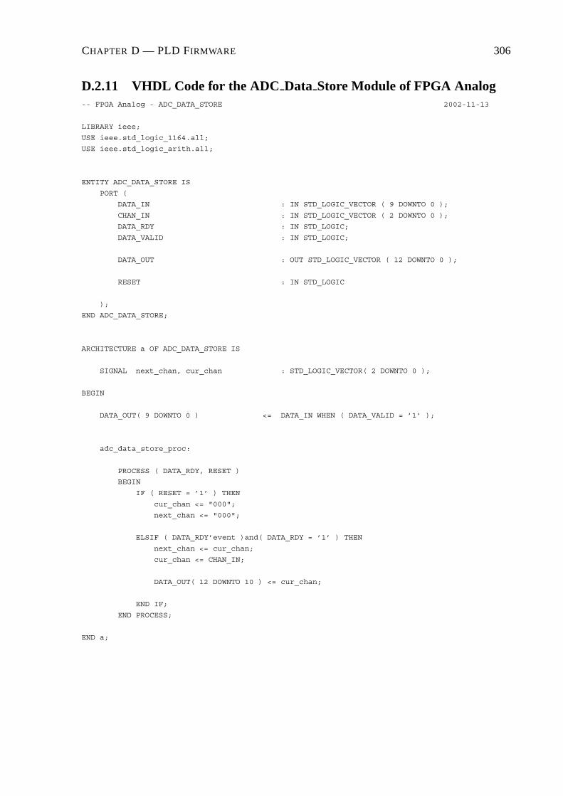
CHAPTER D — PLD FIRMWARE 306
D.2.11 VHDL Code for the ADC Data Store Module of FPGA Analog-- FPGA Analog - ADC_DATA_STORE 2002-11-13
LIBRARY ieee;
USE ieee.std_logic_1164.all;
USE ieee.std_logic_arith.all;
ENTITY ADC_DATA_STORE IS
PORT (
DATA_IN : IN STD_LOGIC_VECTOR ( 9 DOWNTO 0 );
CHAN_IN : IN STD_LOGIC_VECTOR ( 2 DOWNTO 0 );
DATA_RDY : IN STD_LOGIC;
DATA_VALID : IN STD_LOGIC;
DATA_OUT : OUT STD_LOGIC_VECTOR ( 12 DOWNTO 0 );
RESET : IN STD_LOGIC
);
END ADC_DATA_STORE;
ARCHITECTURE a OF ADC_DATA_STORE IS
SIGNAL next_chan, cur_chan : STD_LOGIC_VECTOR( 2 DOWNTO 0 );
BEGIN
DATA_OUT( 9 DOWNTO 0 ) <= DATA_IN WHEN ( DATA_VALID = ’1’ );
adc_data_store_proc:
PROCESS ( DATA_RDY, RESET )
BEGIN
IF ( RESET = ’1’ ) THEN
cur_chan <= "000";
next_chan <= "000";
ELSIF ( DATA_RDY’event )and( DATA_RDY = ’1’ ) THEN
next_chan <= cur_chan;
cur_chan <= CHAN_IN;
DATA_OUT( 12 DOWNTO 10 ) <= cur_chan;
END IF;
END PROCESS;
END a;
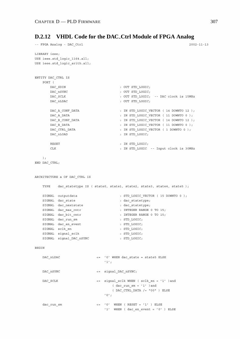
CHAPTER D — PLD FIRMWARE 307
D.2.12 VHDL Code for the DAC Ctrl Module of FPGA Analog-- FPGA Analog - DAC_Ctrl 2002-11-13
LIBRARY ieee;
USE ieee.std_logic_1164.all;
USE ieee.std_logic_arith.all;
ENTITY DAC_CTRL IS
PORT (
DAC_SDIN : OUT STD_LOGIC;
DAC_nSYNC : OUT STD_LOGIC;
DAC_SCLK : OUT STD_LOGIC; -- DAC clock is 15MHz
DAC_nLDAC : OUT STD_LOGIC;
DAC_A_CONF_DATA : IN STD_LOGIC_VECTOR ( 14 DOWNTO 12 );
DAC_A_DATA : IN STD_LOGIC_VECTOR ( 11 DOWNTO 0 );
DAC_B_CONF_DATA : IN STD_LOGIC_VECTOR ( 14 DOWNTO 12 );
DAC_B_DATA : IN STD_LOGIC_VECTOR ( 11 DOWNTO 0 );
DAC_CTRL_DATA : IN STD_LOGIC_VECTOR ( 1 DOWNTO 0 );
DAC_nLOAD : IN STD_LOGIC;
RESET : IN STD_LOGIC;
CLK : IN STD_LOGIC -- Input clock is 30MHz
);
END DAC_CTRL;
ARCHITECTURE a OF DAC_CTRL IS
TYPE dac_statetype IS ( state0, state1, state2, state3, state4, state5 );
SIGNAL outputdata : STD_LOGIC_VECTOR ( 15 DOWNTO 0 );
SIGNAL dac_state : dac_statetype;
SIGNAL dac_nextstate : dac_statetype;
SIGNAL dac_max_cntr : INTEGER RANGE 0 TO 15;
SIGNAL dac_bit_cntr : INTEGER RANGE 0 TO 15;
SIGNAL dac_run_sm : STD_LOGIC;
SIGNAL dac_en_event : STD_LOGIC;
SIGNAL sclk_en : STD_LOGIC;
SIGNAL signal_sclk : STD_LOGIC;
SIGNAL signal_DAC_nSYNC : STD_LOGIC;
BEGIN
DAC_nLDAC <= ’0’ WHEN dac_state = state5 ELSE
’1’;
DAC_nSYNC <= signal_DAC_nSYNC;
DAC_SCLK <= signal_sclk WHEN ( sclk_en = ’1’ )and
( dac_run_sm = ’1’ )and
( DAC_CTRL_DATA /= "00" ) ELSE
’0’;
dac_run_sm <= ’0’ WHEN ( RESET = ’1’ ) ELSE
’1’ WHEN ( dac_en_event = ’0’ ) ELSE

CHAPTER D — PLD FIRMWARE 308
’1’ WHEN ( dac_state /= state0 ) ELSE
’0’;
outputdata( 11 DOWNTO 0 ) <= DAC_A_DATA WHEN ( dac_state = state2 ) ELSE
DAC_B_DATA WHEN ( dac_state = state4 ) ELSE
"000000000000";
outputdata( 14 DOWNTO 12 ) <= DAC_A_CONF_DATA WHEN ( dac_state = state2 ) ELSE
DAC_B_CONF_DATA WHEN ( dac_state = state4 ) ELSE
"000";
outputdata( 15 ) <= ’0’ WHEN ( DAC_CTRL_DATA = "01" ) ELSE
’1’ WHEN ( DAC_CTRL_DATA = "10" ) ELSE
’0’ WHEN ( DAC_CTRL_DATA = "11" )and
( dac_nextstate = state2 ) ELSE
’1’ WHEN ( DAC_CTRL_DATA = "11" )and
( dac_nextstate = state4 ) ELSE
’0’;
------------------------------------------------------------------------------------------
dac_sclk_en_proc:
PROCESS ( CLK, RESET )
BEGIN
IF ( RESET = ’1’ ) THEN
sclk_en <= ’0’;
ELSIF ( CLK’event )and( CLK = ’1’ ) THEN
IF ( dac_state = state2 )or( dac_state = state4 )or
( ( dac_state = state1 )and( dac_bit_cntr = 0) )or
( ( dac_state = state3 )and( dac_bit_cntr = 0) ) THEN
sclk_en <= ’1’;
ELSE
sclk_en <= ’0’;
END IF;
END IF;
END PROCESS dac_sclk_en_proc;
------------------------------------------------------------------------------------------
dac_sclk_proc:
PROCESS ( CLK, RESET )
BEGIN
IF ( RESET = ’1’ ) THEN
signal_sclk <= ’0’;
ELSIF ( CLK’event )and( CLK = ’1’ ) THEN
signal_sclk <= not ( signal_sclk );
END IF;
END PROCESS dac_sclk_proc;

CHAPTER D — PLD FIRMWARE 309
------------------------------------------------------------------------------------------
nsync_proc:
PROCESS ( CLK, RESET )
BEGIN
IF ( RESET = ’1’ ) THEN
signal_DAC_nSYNC <= ’1’;
ELSIF ( CLK’event )and( CLK = ’1’ ) THEN
IF ( dac_state = state2 )or( dac_state = state4)or
( ( dac_state = state1 )and( dac_bit_cntr = 0 ) )or
( ( dac_state = state3 )and( dac_bit_cntr = 0 ) ) THEN
signal_DAC_nSYNC <= ’0’;
ELSE
signal_DAC_nSYNC <= ’1’;
END IF;
END IF;
END PROCESS nsync_proc;
------------------------------------------------------------------------------------------
dac_start_sm:
PROCESS ( RESET, DAC_nLOAD, dac_state )
BEGIN
IF ( RESET = ’1’ )or(dac_state = state1) THEN
dac_en_event <= ’1’;
ELSIF ( DAC_nLOAD’event )and( DAC_nLOAD = ’0’) THEN
dac_en_event <= ’0’;
END IF;
END PROCESS dac_start_sm;
------------------------------------------------------------------------------------------
-- State machine process of DAC
dac_sm_proc:
PROCESS ( dac_state, DAC_CTRL_DATA )
BEGIN
CASE dac_state IS
WHEN state0 =>
dac_max_cntr <= 1;
dac_nextstate <= state1;
WHEN state1 =>
IF ( DAC_CTRL_DATA = "00" ) THEN
dac_nextstate <= state0;
dac_max_cntr <= 0;
ELSIF ( DAC_CTRL_DATA = "01" )or( DAC_CTRL_DATA = "11" ) THEN

CHAPTER D — PLD FIRMWARE 310
dac_nextstate <= state2;
dac_max_cntr <= 14;
ELSE
dac_nextstate <= state4;
dac_max_cntr <= 14;
END IF;
WHEN state2 =>
IF ( DAC_CTRL_DATA = "01" ) THEN
dac_nextstate <= state5;
dac_max_cntr <= 1;
ELSE
dac_nextstate <= state3;
dac_max_cntr <= 1;
END IF;
WHEN state3 =>
dac_max_cntr <= 14;
dac_nextstate <= state4;
WHEN state4 =>
dac_max_cntr <= 1;
dac_nextstate <= state5;
WHEN state5 =>
dac_max_cntr <= 0;
dac_nextstate <= state0;
END CASE;
END PROCESS dac_sm_proc;
------------------------------------------------------------------------------------------
dac_SDIN_proc:
PROCESS ( CLK, RESET )
BEGIN
IF ( RESET = ’1’ ) THEN
DAC_SDIN <= ’0’;
ELSIF ( CLK’event )and( CLK = ’1’ ) THEN
IF ( dac_state = state1 )or( dac_state = state3 ) THEN
DAC_SDIN <= outputdata( 15 );
ELSIF ( dac_state = state2 )or( dac_state = state4 ) THEN
DAC_SDIN <= outputdata( dac_bit_cntr );
ELSE
DAC_SDIN <= ’0’;
END IF;
END IF;
END PROCESS dac_SDIN_proc;
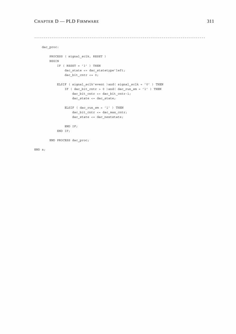
CHAPTER D — PLD FIRMWARE 311
------------------------------------------------------------------------------------------
dac_proc:
PROCESS ( signal_sclk, RESET )
BEGIN
IF ( RESET = ’1’ ) THEN
dac_state <= dac_statetype’left;
dac_bit_cntr <= 0;
ELSIF ( signal_sclk’event )and( signal_sclk = ’0’ ) THEN
IF ( dac_bit_cntr > 0 )and( dac_run_sm = ’1’ ) THEN
dac_bit_cntr <= dac_bit_cntr-1;
dac_state <= dac_state;
ELSIF ( dac_run_sm = ’1’ ) THEN
dac_bit_cntr <= dac_max_cntr;
dac_state <= dac_nextstate;
END IF;
END IF;
END PROCESS dac_proc;
END a;

CHAPTER D — PLD FIRMWARE 312
D.2.13 VHDL Code for the PWM Ctrl Module of FPGA Analog-- FPGA Analog - PWM Controller 2002-11-07
LIBRARY ieee;
USE ieee.std_logic_1164.all;
USE ieee.std_logic_arith.all;
ENTITY pwm_ctrl IS
PORT (
PWMA_TOP : OUT STD_LOGIC;
PWMA_BOT : OUT STD_LOGIC;
PWMB_TOP : OUT STD_LOGIC;
PWMB_BOT : OUT STD_LOGIC;
PWMC_TOP : OUT STD_LOGIC;
PWMC_BOT : OUT STD_LOGIC;
PWMN_TOP : OUT STD_LOGIC;
PWMN_BOT : OUT STD_LOGIC;
ERRA_TOP : IN STD_LOGIC;
ERRA_BOT : IN STD_LOGIC;
ERRB_TOP : IN STD_LOGIC;
ERRB_BOT : IN STD_LOGIC;
ERRC_TOP : IN STD_LOGIC;
ERRC_BOT : IN STD_LOGIC;
ERRN_TOP : IN STD_LOGIC;
ERRN_BOT : IN STD_LOGIC;
TriMax : IN STD_LOGIC_VECTOR ( 9 DOWNTO 0 );
TriFreqScale : IN STD_LOGIC_VECTOR ( 9 DOWNTO 0 );
DeadTime : IN STD_LOGIC_VECTOR ( 9 DOWNTO 0 );
RefA : IN STD_LOGIC_VECTOR ( 9 DOWNTO 0 );
RefB : IN STD_LOGIC_VECTOR ( 9 DOWNTO 0 );
RefC : IN STD_LOGIC_VECTOR ( 9 DOWNTO 0 );
RefN : IN STD_LOGIC_VECTOR ( 9 DOWNTO 0 );
CompUpVal : IN STD_LOGIC_VECTOR ( 9 DOWNTO 0 );
CompDownVal : IN STD_LOGIC_VECTOR ( 9 DOWNTO 0 );
CompUp : OUT STD_LOGIC;
CompDown : OUT STD_LOGIC;
RampDir : OUT STD_LOGIC;
CounterZero : OUT STD_LOGIC;
PWM_nEN : IN STD_LOGIC;
RESET : IN STD_LOGIC;
CLK : IN STD_LOGIC
);
END pwm_ctrl;
ARCHITECTURE a OF pwm_ctrl IS
TYPE gate_state_type IS ( topstate, deadstate, botstate );
SIGNAL slow_clk : STD_LOGIC;
SIGNAL clk_cntr : INTEGER RANGE 0 TO 1023;

CHAPTER D — PLD FIRMWARE 313
SIGNAL signal_PWM_nEN : STD_LOGIC;
SIGNAL pwm_error : STD_LOGIC;
SIGNAL signal_TriFreqScale : INTEGER RANGE 0 TO 1023;
SIGNAL rampcntr : INTEGER RANGE 0 TO 1023;
SIGNAL signal_rampdir : STD_LOGIC;
SIGNAL signal_trimax : INTEGER RANGE 0 TO 1023;
SIGNAL phase_a_state : gate_state_type;
SIGNAL signal_RefA : INTEGER RANGE 0 TO 1023;
SIGNAL deadtimecntr_a : INTEGER RANGE 0 TO 1023;
SIGNAL phase_b_state : gate_state_type;
SIGNAL signal_RefB : INTEGER RANGE 0 TO 1023;
SIGNAL deadtimecntr_b : INTEGER RANGE 0 TO 1023;
SIGNAL phase_c_state : gate_state_type;
SIGNAL signal_RefC : INTEGER RANGE 0 TO 1023;
SIGNAL deadtimecntr_c : INTEGER RANGE 0 TO 1023;
SIGNAL phase_n_state : gate_state_type;
SIGNAL signal_RefN : INTEGER RANGE 0 TO 1023;
SIGNAL deadtimecntr_n : INTEGER RANGE 0 TO 1023;
SIGNAL signal_PWMA_TOP : STD_LOGIC;
SIGNAL signal_PWMA_BOT : STD_LOGIC;
SIGNAL signal_PWMB_TOP : STD_LOGIC;
SIGNAL signal_PWMB_BOT : STD_LOGIC;
SIGNAL signal_PWMC_TOP : STD_LOGIC;
SIGNAL signal_PWMC_BOT : STD_LOGIC;
SIGNAL signal_PWMN_TOP : STD_LOGIC;
SIGNAL signal_PWMN_BOT : STD_LOGIC;
BEGIN
signal_RefA <= CONV_INTEGER( UNSIGNED ( RefA ) );
signal_RefB <= CONV_INTEGER( UNSIGNED ( RefB ) );
signal_RefC <= CONV_INTEGER( UNSIGNED ( RefC ) );
signal_RefN <= CONV_INTEGER( UNSIGNED ( RefN ) );
PWMA_TOP <= not signal_PWMA_TOP;
PWMA_BOT <= not signal_PWMA_BOT;
PWMB_TOP <= not signal_PWMB_TOP;
PWMB_BOT <= not signal_PWMB_BOT;
PWMC_TOP <= not signal_PWMC_TOP;
PWMC_BOT <= not signal_PWMC_BOT;
PWMN_TOP <= not signal_PWMN_TOP;
PWMN_BOT <= not signal_PWMN_BOT;
signal_trimax <= CONV_INTEGER( UNSIGNED ( TriMax ) );
RampDir <= signal_rampdir;
signal_TriFreqScale <= CONV_INTEGER( UNSIGNED ( TriFreqScale ) );
------------------------------------------------------------------------------------------

CHAPTER D — PLD FIRMWARE 314
ref_proc:
PROCESS ( CLK, RESET )
BEGIN
IF ( RESET = ’1’ ) THEN
CounterZero <= ’1’;
ELSIF ( CLK’event )and( CLK = ’1’ ) THEN
IF ( rampcntr = 0 ) THEN
CounterZero <= ’1’;
ELSE
CounterZero <= ’0’;
END IF;
END IF;
END PROCESS ref_proc;
------------------------------------------------------------------------------------------
phase_a_sm_ctrl_proc:
PROCESS ( slow_clk, RESET )
BEGIN
IF ( RESET = ’1’ ) THEN
signal_PWMA_TOP <= ’0’;
signal_PWMA_BOT <= ’0’;
deadtimecntr_a <= 0;
phase_a_state <= topstate;
ELSIF ( slow_clk’event )and( slow_clk = ’1’ ) THEN
IF ( signal_PWM_nEN = ’1’ ) THEN
phase_a_state <= topstate;
signal_PWMA_TOP <= ’0’;
signal_PWMA_BOT <= ’0’;
deadtimecntr_a <= 0;
ELSIF ( phase_a_state = topstate )and( rampcntr < signal_RefA ) THEN
phase_a_state <= topstate;
signal_PWMA_TOP <= ’1’;
signal_PWMA_BOT <= ’0’;
deadtimecntr_a <= 0;
ELSIF ( phase_a_state = topstate ) THEN
phase_a_state <= deadstate;
signal_PWMA_TOP <= ’0’;
signal_PWMA_BOT <= ’0’;
deadtimecntr_a <= deadtimecntr_a + 1;
ELSIF ( phase_a_state = deadstate )and
( deadtimecntr_a < CONV_INTEGER( UNSIGNED ( DeadTime ) ) )and
( signal_rampdir = ’1’ ) THEN
phase_a_state <= deadstate;
signal_PWMA_TOP <= ’0’;
signal_PWMA_BOT <= ’0’;
deadtimecntr_a <= deadtimecntr_a + 1;
ELSIF ( phase_a_state = deadstate )and( signal_rampdir = ’1’ ) THEN

CHAPTER D — PLD FIRMWARE 315
phase_a_state <= botstate;
signal_PWMA_TOP <= ’0’;
signal_PWMA_BOT <= ’1’;
deadtimecntr_a <= 0;
ELSIF ( phase_a_state = botstate )and( rampcntr > signal_RefA ) THEN
phase_a_state <= botstate;
signal_PWMA_TOP <= ’0’;
signal_PWMA_BOT <= ’1’;
deadtimecntr_a <= 0;
ELSIF ( phase_a_state = botstate ) THEN
phase_a_state <= deadstate;
signal_PWMA_TOP <= ’0’;
signal_PWMA_BOT <= ’0’;
deadtimecntr_a <= 0;
ELSIF ( phase_a_state = deadstate )and
( deadtimecntr_a < CONV_INTEGER( UNSIGNED ( DeadTime ) ) )and
( signal_rampdir = ’0’ ) THEN
phase_a_state <= deadstate;
signal_PWMA_TOP <= ’0’;
signal_PWMA_BOT <= ’0’;
deadtimecntr_a <= deadtimecntr_a + 1;
ELSIF ( phase_a_state = deadstate )and( signal_rampdir = ’0’ ) THEN
phase_a_state <= topstate;
signal_PWMA_TOP <= ’1’;
signal_PWMA_BOT <= ’0’;
deadtimecntr_a <= 0;
END IF;
END IF;
END PROCESS phase_a_sm_ctrl_proc;
------------------------------------------------------------------------------------------
phase_b_sm_ctrl_proc:
PROCESS ( slow_clk, RESET )
BEGIN
IF ( RESET = ’1’ ) THEN
signal_PWMB_TOP <= ’0’;
signal_PWMB_BOT <= ’0’;
deadtimecntr_b <= 0;
phase_b_state <= topstate;
ELSIF ( slow_clk’event )and( slow_clk = ’1’ ) THEN
IF ( signal_PWM_nEN = ’1’ ) THEN
phase_b_state <= topstate;
signal_PWMB_TOP <= ’0’;
signal_PWMB_BOT <= ’0’;
deadtimecntr_b <= 0;
ELSIF ( phase_b_state = topstate )and( rampcntr < signal_RefB ) THEN
phase_b_state <= topstate;
signal_PWMB_TOP <= ’1’;
signal_PWMB_BOT <= ’0’;

CHAPTER D — PLD FIRMWARE 316
deadtimecntr_b <= 0;
ELSIF ( phase_b_state = topstate ) THEN
phase_b_state <= deadstate;
signal_PWMB_TOP <= ’0’;
signal_PWMB_BOT <= ’0’;
deadtimecntr_b <= deadtimecntr_b + 1;
ELSIF ( phase_b_state = deadstate )and
( deadtimecntr_b < CONV_INTEGER( UNSIGNED ( DeadTime ) ) )and
( signal_rampdir = ’1’ ) THEN
phase_b_state <= deadstate;
signal_PWMB_TOP <= ’0’;
signal_PWMB_BOT <= ’0’;
deadtimecntr_b <= deadtimecntr_b + 1;
ELSIF ( phase_b_state = deadstate )and( signal_rampdir = ’1’ ) THEN
phase_b_state <= botstate;
signal_PWMB_TOP <= ’0’;
signal_PWMB_BOT <= ’1’;
deadtimecntr_b <= 0;
ELSIF ( phase_b_state = botstate )and( rampcntr > signal_RefB ) THEN
phase_b_state <= botstate;
signal_PWMB_TOP <= ’0’;
signal_PWMB_BOT <= ’1’;
deadtimecntr_b <= 0;
ELSIF ( phase_b_state = botstate ) THEN
phase_b_state <= deadstate;
signal_PWMB_TOP <= ’0’;
signal_PWMB_BOT <= ’0’;
deadtimecntr_b <= 0;
ELSIF ( phase_b_state = deadstate )and
( deadtimecntr_b < CONV_INTEGER( UNSIGNED ( DeadTime ) ) )and
( signal_rampdir = ’0’ ) THEN
phase_b_state <= deadstate;
signal_PWMB_TOP <= ’0’;
signal_PWMB_BOT <= ’0’;
deadtimecntr_b <= deadtimecntr_b + 1;
ELSIF ( phase_b_state = deadstate )and( signal_rampdir = ’0’ ) THEN
phase_b_state <= topstate;
signal_PWMB_TOP <= ’1’;
signal_PWMB_BOT <= ’0’;
deadtimecntr_b <= 0;
END IF;
END IF;
END PROCESS phase_b_sm_ctrl_proc;
------------------------------------------------------------------------------------------
phase_c_sm_ctrl_proc:
PROCESS ( slow_clk, RESET )
BEGIN
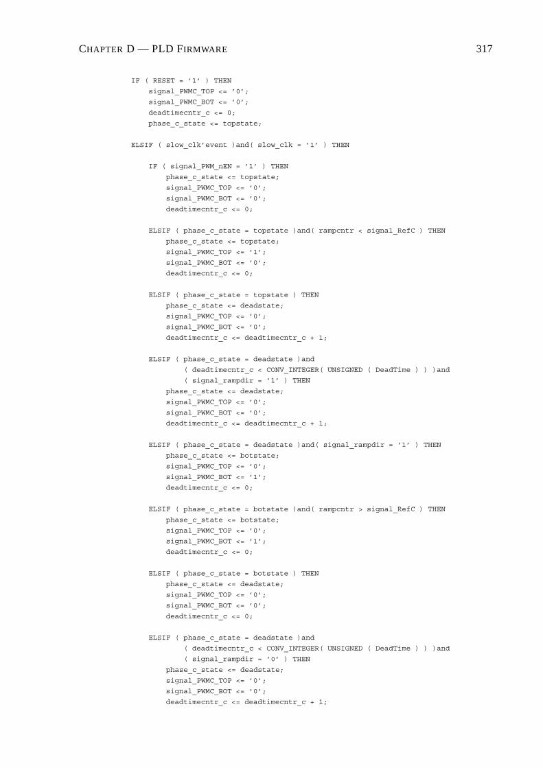
CHAPTER D — PLD FIRMWARE 317
IF ( RESET = ’1’ ) THEN
signal_PWMC_TOP <= ’0’;
signal_PWMC_BOT <= ’0’;
deadtimecntr_c <= 0;
phase_c_state <= topstate;
ELSIF ( slow_clk’event )and( slow_clk = ’1’ ) THEN
IF ( signal_PWM_nEN = ’1’ ) THEN
phase_c_state <= topstate;
signal_PWMC_TOP <= ’0’;
signal_PWMC_BOT <= ’0’;
deadtimecntr_c <= 0;
ELSIF ( phase_c_state = topstate )and( rampcntr < signal_RefC ) THEN
phase_c_state <= topstate;
signal_PWMC_TOP <= ’1’;
signal_PWMC_BOT <= ’0’;
deadtimecntr_c <= 0;
ELSIF ( phase_c_state = topstate ) THEN
phase_c_state <= deadstate;
signal_PWMC_TOP <= ’0’;
signal_PWMC_BOT <= ’0’;
deadtimecntr_c <= deadtimecntr_c + 1;
ELSIF ( phase_c_state = deadstate )and
( deadtimecntr_c < CONV_INTEGER( UNSIGNED ( DeadTime ) ) )and
( signal_rampdir = ’1’ ) THEN
phase_c_state <= deadstate;
signal_PWMC_TOP <= ’0’;
signal_PWMC_BOT <= ’0’;
deadtimecntr_c <= deadtimecntr_c + 1;
ELSIF ( phase_c_state = deadstate )and( signal_rampdir = ’1’ ) THEN
phase_c_state <= botstate;
signal_PWMC_TOP <= ’0’;
signal_PWMC_BOT <= ’1’;
deadtimecntr_c <= 0;
ELSIF ( phase_c_state = botstate )and( rampcntr > signal_RefC ) THEN
phase_c_state <= botstate;
signal_PWMC_TOP <= ’0’;
signal_PWMC_BOT <= ’1’;
deadtimecntr_c <= 0;
ELSIF ( phase_c_state = botstate ) THEN
phase_c_state <= deadstate;
signal_PWMC_TOP <= ’0’;
signal_PWMC_BOT <= ’0’;
deadtimecntr_c <= 0;
ELSIF ( phase_c_state = deadstate )and
( deadtimecntr_c < CONV_INTEGER( UNSIGNED ( DeadTime ) ) )and
( signal_rampdir = ’0’ ) THEN
phase_c_state <= deadstate;
signal_PWMC_TOP <= ’0’;
signal_PWMC_BOT <= ’0’;
deadtimecntr_c <= deadtimecntr_c + 1;

CHAPTER D — PLD FIRMWARE 318
ELSIF ( phase_c_state = deadstate )and( signal_rampdir = ’0’ ) THEN
phase_c_state <= topstate;
signal_PWMC_TOP <= ’1’;
signal_PWMC_BOT <= ’0’;
deadtimecntr_c <= 0;
END IF;
END IF;
END PROCESS phase_c_sm_ctrl_proc;
------------------------------------------------------------------------------------------
phase_n_sm_ctrl_proc:
PROCESS ( slow_clk, RESET )
BEGIN
IF ( RESET = ’1’ ) THEN
signal_PWMN_TOP <= ’0’;
signal_PWMN_BOT <= ’0’;
deadtimecntr_n <= 0;
phase_n_state <= topstate;
ELSIF ( slow_clk’event )and( slow_clk = ’1’ ) THEN
IF ( signal_PWM_nEN = ’1’ ) THEN
phase_n_state <= topstate;
signal_PWMN_TOP <= ’0’;
signal_PWMN_BOT <= ’0’;
deadtimecntr_n <= 0;
ELSIF ( phase_n_state = topstate )and( rampcntr < signal_RefN ) THEN
phase_n_state <= topstate;
signal_PWMN_TOP <= ’1’;
signal_PWMN_BOT <= ’0’;
deadtimecntr_n <= 0;
ELSIF ( phase_n_state = topstate ) THEN
phase_n_state <= deadstate;
signal_PWMN_TOP <= ’0’;
signal_PWMN_BOT <= ’0’;
deadtimecntr_n <= deadtimecntr_n + 1;
ELSIF ( phase_n_state = deadstate )and
( deadtimecntr_n < CONV_INTEGER( UNSIGNED ( DeadTime ) ) )and
( signal_rampdir = ’1’ ) THEN
phase_n_state <= deadstate;
signal_PWMN_TOP <= ’0’;
signal_PWMN_BOT <= ’0’;
deadtimecntr_n <= deadtimecntr_n + 1;
ELSIF ( phase_n_state = deadstate )and( signal_rampdir = ’1’ ) THEN
phase_n_state <= botstate;
signal_PWMN_TOP <= ’0’;
signal_PWMN_BOT <= ’1’;
deadtimecntr_n <= 0;
ELSIF ( phase_n_state = botstate )and( rampcntr > signal_RefN ) THEN

CHAPTER D — PLD FIRMWARE 319
phase_n_state <= botstate;
signal_PWMN_TOP <= ’0’;
signal_PWMN_BOT <= ’1’;
deadtimecntr_n <= 0;
ELSIF ( phase_n_state = botstate ) THEN
phase_n_state <= deadstate;
signal_PWMN_TOP <= ’0’;
signal_PWMN_BOT <= ’0’;
deadtimecntr_n <= 0;
ELSIF ( phase_n_state = deadstate )and
( deadtimecntr_n < CONV_INTEGER( UNSIGNED ( DeadTime ) ) )and
( signal_rampdir = ’0’ ) THEN
phase_n_state <= deadstate;
signal_PWMN_TOP <= ’0’;
signal_PWMN_BOT <= ’0’;
deadtimecntr_n <= deadtimecntr_n + 1;
ELSIF ( phase_n_state = deadstate )and( signal_rampdir = ’0’ ) THEN
phase_n_state <= topstate;
signal_PWMN_TOP <= ’1’;
signal_PWMN_BOT <= ’0’;
deadtimecntr_n <= 0;
END IF;
END IF;
END PROCESS phase_n_sm_ctrl_proc;
------------------------------------------------------------------------------------------
compup_proc:
PROCESS ( CLK, RESET )
BEGIN
IF ( RESET = ’1’ ) THEN
CompUp <= ’0’;
ELSIF ( CLK’event )and( CLK = ’1’ ) THEN
IF ( signal_PWM_nEN = ’1’ ) THEN
CompUp <= ’0’;
ELSIF ( signal_rampdir = ’1’ )and
( rampcntr < CONV_INTEGER( UNSIGNED ( CompUpVal ) ) ) THEN
CompUp <= ’0’;
ELSIF ( rampcntr >= CONV_INTEGER( UNSIGNED ( CompUpVal ) ) ) THEN
CompUp <= ’1’;
END IF;
END IF;
END PROCESS compup_proc;
------------------------------------------------------------------------------------------
compdown_proc:

CHAPTER D — PLD FIRMWARE 320
PROCESS ( CLK, RESET )
BEGIN
IF ( RESET = ’1’ ) THEN
CompDown <= ’0’;
ELSIF ( CLK’event )and( CLK = ’1’ ) THEN
IF ( signal_PWM_nEN = ’1’ ) THEN
CompDown <= ’0’;
ELSIF ( signal_rampdir = ’1’ ) THEN
CompDown <= ’0’;
ELSIF ( signal_rampdir = ’0’ )and
( rampcntr <= CONV_INTEGER( UNSIGNED ( CompDownVal ) ) ) THEN
CompDown <= ’1’;
ELSIF ( rampcntr >= CONV_INTEGER( UNSIGNED ( CompDownVal ) ) ) THEN
CompDown <= ’0’;
END IF;
END IF;
END PROCESS compdown_proc;
------------------------------------------------------------------------------------------
pwm_error_proc:
PROCESS ( CLK, RESET )
BEGIN
IF ( RESET = ’1’ ) THEN
pwm_error <= ’0’;
ELSIF ( CLK’event )and( CLK = ’1’ ) THEN
IF ( ( signal_PWMA_TOP = ’1’ )and( signal_PWMA_BOT = ’1’ ) )or
( ( signal_PWMB_TOP = ’1’ )and( signal_PWMB_BOT = ’1’ ) )or
( ( signal_PWMC_TOP = ’1’ )and( signal_PWMC_BOT = ’1’ ) )or
( ( signal_PWMN_TOP = ’1’ )and( signal_PWMN_BOT = ’1’ ) ) THEN
pwm_error <= ’1’;
END IF;
END IF;
END PROCESS pwm_error_proc;
------------------------------------------------------------------------------------------
pwm_nen_proc:
PROCESS ( CLK, RESET, PWM_nEN )
BEGIN
IF ( RESET = ’1’ ) THEN
signal_PWM_nEN <= PWM_nEN;
ELSIF ( CLK’event )and( CLK = ’1’ ) THEN
IF ( pwm_error = ’1’ ) THEN
signal_PWM_nEN <= ’1’;

CHAPTER D — PLD FIRMWARE 321
ELSE
signal_PWM_nEN <= PWM_nEN;
END IF;
END IF;
END PROCESS pwm_nen_proc;
------------------------------------------------------------------------------------------
ramp_cntr_proc:
PROCESS ( slow_clk, RESET )
BEGIN
IF ( RESET = ’1’ ) THEN
signal_rampdir <= ’1’;
rampcntr <= 0;
ELSIF ( slow_clk’event )and( slow_clk = ’1’ ) THEN
IF ( signal_rampdir = ’1’ )and( rampcntr < signal_trimax )and
( signal_PWM_nEN = ’0’ ) THEN
rampcntr <= rampcntr + 1;
signal_rampdir <= ’1’;
ELSIF ( signal_rampdir = ’0’ )and( rampcntr > 0 )and
( signal_PWM_nEN = ’0’ ) THEN
rampcntr <= rampcntr - 1;
signal_rampdir <= ’0’;
ELSIF ( signal_PWM_nEN = ’0’ ) THEN
rampcntr <= rampcntr;
signal_rampdir <= not ( signal_rampdir );
END IF;
END IF;
END PROCESS ramp_cntr_proc;
------------------------------------------------------------------------------------------
clk_proc:
PROCESS ( CLK, RESET )
BEGIN
IF ( RESET = ’1’ ) THEN
clk_cntr <= 0;
slow_clk <= ’1’;
ELSIF ( CLK’event )and( CLK = ’1’ ) THEN
IF ( clk_cntr < signal_TriFreqScale ) THEN
clk_cntr <= clk_cntr+1;
slow_clk <= slow_clk;
ELSE
clk_cntr <= 0;
slow_clk <= not ( slow_clk );
END IF;

CHAPTER D — PLD FIRMWARE 322
END IF;
END PROCESS clk_proc;
END a;

CHAPTER D — PLD FIRMWARE 323
D.2.14 VHDL Code for the LCD Ctrl Module of FPGA Analog--PEC33 Analog - LCD_Ctrl 2002-11-13
LIBRARY ieee;
USE ieee.std_logic_1164.all;
USE ieee.std_logic_arith.all;
ENTITY LCD_CTRL IS
PORT (
LCD_DATA : INOUT STD_LOGIC_VECTOR( 7 DOWNTO 0 );
LCD_E : OUT STD_LOGIC;
LCD_RnW : OUT STD_LOGIC;
LCD_RS : OUT STD_LOGIC;
LCD_RDYnBSY : OUT STD_LOGIC;
LCD_MODE_DATA : IN STD_LOGIC_VECTOR ( 7 DOWNTO 0 );
LCD_UPDATE_MODE : IN STD_LOGIC;
LCD_CHAR : IN STD_LOGIC_VECTOR ( 7 DOWNTO 0 );
LCD_ADDR : IN STD_LOGIC_VECTOR ( 6 DOWNTO 0 );
LCD_UPDATE_DATA : IN STD_LOGIC;
LCD_RESET : IN STD_LOGIC; -- Resets/Initialises the LCD
RESET : IN STD_LOGIC; -- Resets the LCD controller
CLK : IN STD_LOGIC -- Input clock is 30MHz
);
END LCD_CTRL;
ARCHITECTURE a OF LCD_CTRL IS
TYPE lcd_statetype IS ( idlestate, resetstate, modestate, datastate );
TYPE data_statetype IS ( nodatastate, modedatastate, addrstate, charstate, def0state,
def1state, def2state, def3state, def4state );
TYPE statetype IS ( state0, state1, state2, state3, BFstate );
constant def0 : STD_LOGIC_VECTOR := "00111100";
constant def1 : STD_LOGIC_VECTOR := "00111100";
constant def2 : STD_LOGIC_VECTOR := "00001110";
constant def3 : STD_LOGIC_VECTOR := "00000110";
constant def4 : STD_LOGIC_VECTOR := "00000001";
SIGNAL lcd_state : lcd_statetype;
SIGNAL data_state : data_statetype;
SIGNAL nextdata_state : data_statetype;
SIGNAL wr_state : statetype;
SIGNAL nextwr_state : statetype;
SIGNAL rd_state : statetype;
SIGNAL nextrd_state : statetype;
SIGNAL signal_LCD_ADDR : STD_LOGIC_VECTOR ( 7 DOWNTO 0 );
SIGNAL outputdata : STD_LOGIC_VECTOR ( 7 DOWNTO 0 );
SIGNAL inputdata : STD_LOGIC_VECTOR ( 7 DOWNTO 0 );
SIGNAL reset_event : STD_LOGIC;
SIGNAL updatemode_event : STD_LOGIC;
SIGNAL updatedata_event : STD_LOGIC;
SIGNAL datawritten_event : STD_LOGIC;

CHAPTER D — PLD FIRMWARE 324
SIGNAL char_cntr : INTEGER RANGE 0 TO 8;
SIGNAL max_char_cntr : INTEGER RANGE 0 TO 8;
SIGNAL data_sm_running : STD_LOGIC;
SIGNAL strt_data_sm : STD_LOGIC;
SIGNAL next_wr_sm_cntr : INTEGER RANGE 0 TO 4095;
SIGNAL wr_sm_cntr : INTEGER RANGE 0 TO 4095;
SIGNAL wr_sm_running : STD_LOGIC;
SIGNAL strt_wr_sm : STD_LOGIC;
SIGNAL next_rd_sm_cntr : INTEGER RANGE 0 TO 4095;
SIGNAL rd_sm_cntr : INTEGER RANGE 0 TO 4095;
SIGNAL rd_sm_running : STD_LOGIC;
SIGNAL strt_rd_sm : STD_LOGIC;
SIGNAL RnWData : STD_LOGIC;
SIGNAL RDYnBSY : STD_LOGIC;
COMPONENT Bidir
GENERIC (
n : INTEGER RANGE 0 TO 31 := 15
);
PORT (
BIDIR : INOUT STD_LOGIC_VECTOR ( n DOWNTO 0 );
RnW : IN STD_LOGIC;
CLK : IN STD_LOGIC;
IN_DATA : IN STD_LOGIC_VECTOR ( n DOWNTO 0 );
OUT_DATA : OUT STD_LOGIC_VECTOR ( n DOWNTO 0 )
);
END COMPONENT;
BEGIN
signal_LCD_ADDR ( 7 ) <= ’1’;
signal_LCD_ADDR ( 6 DOWNTO 0 ) <= LCD_ADDR;
outputdata
<= "00000010" WHEN ( lcd_state = datastate )and
( data_state = modedatastate ) ELSE
LCD_MODE_DATA WHEN ( lcd_state = modestate )and
( data_state = modedatastate ) ELSE
def0 WHEN ( lcd_state = resetstate )and( data_state = def0state ) ELSE
def1 WHEN ( lcd_state = resetstate )and( data_state = def1state ) ELSE
def2 WHEN ( lcd_state = resetstate )and( data_state = def2state ) ELSE
def3 WHEN ( lcd_state = resetstate )and( data_state = def3state ) ELSE
def4 WHEN ( lcd_state = resetstate )and( data_state = def4state ) ELSE
signal_LCD_ADDR WHEN ( lcd_state = datastate )and
( data_state = addrstate ) ELSE
LCD_CHAR WHEN ( lcd_state = datastate )and( data_state = charstate ) ELSE
"00000000";
RnWdata
<= ’1’ WHEN ( rd_state = state3 )or( rd_state = BFstate ) ELSE

CHAPTER D — PLD FIRMWARE 325
’0’ WHEN ( ( wr_state = state2 )or( wr_state = state3 ) )and
( rd_state = state0 ) ELSE
’1’;
LCD_RDYnBSY
<= ’1’ WHEN ( lcd_state = idlestate )and( data_state = nodatastate ) ELSE
’0’;
reset_event
<= ’0’ WHEN ( RESET = ’1’ ) ELSE
’1’ WHEN ( LCD_RESET = ’0’ )and
( ( lcd_state = idlestate )or( lcd_state = resetstate ) ) ELSE
’0’;
updatemode_event
<= ’0’ WHEN ( RESET = ’1’ ) ELSE
’1’ WHEN ( LCD_UPDATE_MODE = ’0’ )and
( ( lcd_state = idlestate )or( lcd_state = modestate ) ) ELSE
’0’;
updatedata_event
<= ’0’ WHEN ( RESET = ’1’ ) ELSE
’1’ WHEN ( LCD_UPDATE_DATA = ’0’ )and
( ( lcd_state = idlestate )or( lcd_state = datastate ) ) ELSE
’0’;
datawritten_event
<= ’0’ WHEN ( RESET = ’1’ ) ELSE
’1’ WHEN ( wr_state = BFstate )and( nextrd_state = state0 ) ELSE
’0’;
data_sm_running
<= ’0’ WHEN ( RESET = ’1’ ) ELSE
’0’ WHEN ( wr_state /= state0 ) ELSE
’0’ WHEN ( strt_data_sm = ’1’ ) ELSE
’1’ WHEN ( data_state /= nodatastate ) ELSE
’0’;
max_char_cntr
<= 0; --1 WHEN ( data_state = charstate ) ELSE
--0;
wr_sm_running
<= ’0’ WHEN ( RESET = ’1’ ) ELSE
’1’ WHEN ( datawritten_event = ’1’ ) ELSE
’0’ WHEN ( rd_state /= state0 ) ELSE
’1’ WHEN ( wr_state /= state0 )and
( lcd_state /= idlestate )and( rd_sm_running = ’0’ ) ELSE
’0’;
rd_sm_running
<= ’1’ WHEN ( rd_state /= state0 )and( lcd_state /= idlestate ) ELSE

CHAPTER D — PLD FIRMWARE 326
’0’;
RDYnBSY
<= not ( inputdata(7) );
------------------------------------------------------------------------------------------
bidir_bus_map:
bidir GENERIC MAP ( n => 7 )
PORT MAP ( BIDIR => LCD_DATA, RnW => RnWdata, CLK => CLK,
IN_DATA => outputdata, OUT_DATA => inputdata );
------------------------------------------------------------------------------------------
lcd_rs_proc:
PROCESS ( CLK, RESET )
BEGIN
IF ( RESET = ’1’ ) THEN
LCD_RS <= ’0’;
ELSIF ( CLK’event )and( CLK = ’1’ ) THEN
IF ( data_state = charstate ) THEN
LCD_RS <= ’1’;
ELSE
LCD_RS <= ’0’;
END IF;
END IF;
END PROCESS lcd_rs_proc;
------------------------------------------------------------------------------------------
lcd_e_proc:
PROCESS ( CLK, RESET )
BEGIN
IF ( RESET = ’1’ ) THEN
LCD_E <= ’0’;
ELSIF ( CLK’event )and( CLK = ’1’ ) THEN
IF ( rd_state = state2 )or( wr_state = state2 ) THEN
LCD_E <= ’1’;
ELSE
LCD_E <= ’0’;
END IF;
END IF;
END PROCESS lcd_e_proc;
------------------------------------------------------------------------------------------
lcd_rnw_proc:

CHAPTER D — PLD FIRMWARE 327
PROCESS ( CLK, RESET )
BEGIN
IF ( RESET = ’1’ ) THEN
LCD_RnW <= ’0’;
ELSIF ( CLK’event )and( CLK = ’1’ ) THEN
IF ( rd_state /= state0 ) THEN
LCD_RnW <= ’1’;
ELSE
LCD_RnW <= ’0’;
END IF;
END IF;
END PROCESS lcd_rnw_proc;
------------------------------------------------------------------------------------------
lcd_state_ctrl_proc:
PROCESS ( CLK, RESET )
BEGIN
IF ( RESET = ’1’ ) THEN
lcd_state <= idlestate;
ELSIF ( CLK’event )and( CLK = ’1’ ) THEN
IF ( reset_event = ’1’ ) THEN
lcd_state <= resetstate;
ELSIF ( updatemode_event = ’1’ ) THEN
lcd_state <= modestate;
ELSIF ( updatedata_event = ’1’ ) THEN
lcd_state <= datastate;
ELSIF ( data_state = nodatastate ) THEN
lcd_state <= idlestate;
END IF;
END IF;
END PROCESS lcd_state_ctrl_proc;
------------------------------------------------------------------------------------------
data_state_sm_proc:
PROCESS ( data_state, lcd_state )
BEGIN
CASE data_state IS
WHEN nodatastate =>
IF ( lcd_state = modestate ) THEN
nextdata_state <= modedatastate;
ELSIF ( lcd_state = datastate ) THEN
nextdata_state <= addrstate;
ELSIF ( lcd_state = resetstate ) THEN
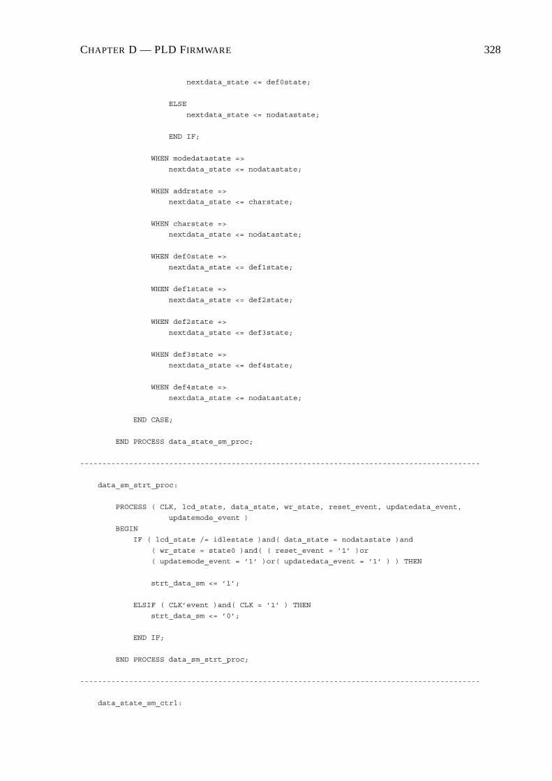
CHAPTER D — PLD FIRMWARE 328
nextdata_state <= def0state;
ELSE
nextdata_state <= nodatastate;
END IF;
WHEN modedatastate =>
nextdata_state <= nodatastate;
WHEN addrstate =>
nextdata_state <= charstate;
WHEN charstate =>
nextdata_state <= nodatastate;
WHEN def0state =>
nextdata_state <= def1state;
WHEN def1state =>
nextdata_state <= def2state;
WHEN def2state =>
nextdata_state <= def3state;
WHEN def3state =>
nextdata_state <= def4state;
WHEN def4state =>
nextdata_state <= nodatastate;
END CASE;
END PROCESS data_state_sm_proc;
------------------------------------------------------------------------------------------
data_sm_strt_proc:
PROCESS ( CLK, lcd_state, data_state, wr_state, reset_event, updatedata_event,
updatemode_event )
BEGIN
IF ( lcd_state /= idlestate )and( data_state = nodatastate )and
( wr_state = state0 )and( ( reset_event = ’1’ )or
( updatemode_event = ’1’ )or( updatedata_event = ’1’ ) ) THEN
strt_data_sm <= ’1’;
ELSIF ( CLK’event )and( CLK = ’1’ ) THEN
strt_data_sm <= ’0’;
END IF;
END PROCESS data_sm_strt_proc;
------------------------------------------------------------------------------------------
data_state_sm_ctrl:

CHAPTER D — PLD FIRMWARE 329
PROCESS ( CLK, RESET )
BEGIN
IF ( RESET = ’1’ ) THEN
data_state <= nodatastate;
ELSIF ( CLK’event )and( CLK = ’1’ ) THEN
IF ( strt_data_sm = ’1’ )and( data_state = nodatastate ) THEN
data_state <= nextdata_state;
ELSIF ( data_sm_running = ’1’ ) THEN
data_state <= nextdata_state;
END IF;
END IF;
END PROCESS data_state_sm_ctrl;
------------------------------------------------------------------------------------------
wr_state_sm_proc:
PROCESS ( wr_state )
BEGIN
CASE wr_state IS
WHEN state0 =>
next_wr_sm_cntr <= 1500;
nextwr_state <= BFstate;
WHEN BFstate =>
next_wr_sm_cntr <= 1;
nextwr_state <= state1;
WHEN state1 =>
next_wr_sm_cntr <= 6;
nextwr_state <= state2;
WHEN state2 =>
next_wr_sm_cntr <= 8;
nextwr_state <= state3;
WHEN state3 =>
next_wr_sm_cntr <= 5;
nextwr_state <= state0;
END CASE;
END PROCESS wr_state_sm_proc;
------------------------------------------------------------------------------------------
wr_sm_strt_proc:
PROCESS ( CLK, data_state, wr_state, lcd_state, nextdata_state, reset_event,
updatedata_event, updatemode_event )
BEGIN
IF ( data_state /= nodatastate )and( wr_state = state0 )and
( lcd_state /= idlestate )and( ( nextdata_state /= nodatastate )or
( reset_event = ’1’ )or( updatemode_event = ’1’ )or
( updatedata_event = ’1’ ) ) THEN

CHAPTER D — PLD FIRMWARE 330
strt_wr_sm <= ’1’;
ELSIF ( CLK’event )and( CLK = ’0’ ) THEN
strt_wr_sm <= ’0’;
END IF;
END PROCESS wr_sm_strt_proc;
------------------------------------------------------------------------------------------
wr_state_sm_ctrl:
PROCESS ( CLK, RESET )
BEGIN
IF ( RESET = ’1’ ) THEN
wr_state <= state0;
wr_sm_cntr <= 1;
char_cntr <= 0;
ELSIF ( CLK’event )and( CLK = ’1’ ) THEN
IF ( strt_wr_sm = ’1’ ) THEN
wr_sm_cntr <= next_wr_sm_cntr;
wr_state <= nextwr_state;
ELSIF ( wr_sm_running = ’1’)and( wr_sm_cntr > 0 ) THEN
wr_sm_cntr <= wr_sm_cntr-1;
wr_state <= wr_state;
ELSIF ( wr_sm_running = ’1’) THEN
wr_sm_cntr <= next_wr_sm_cntr;
wr_state <= nextwr_state;
END IF;
END IF;
END PROCESS wr_state_sm_ctrl;
------------------------------------------------------------------------------------------
rd_state_sm_proc:
PROCESS ( rd_state, RDYnBSY )
BEGIN
CASE rd_state IS
WHEN state0 =>
next_rd_sm_cntr <= 1;
nextrd_state <= state1;
WHEN state1 =>
next_rd_sm_cntr <= 6;
nextrd_state <= state2;
WHEN state2 =>
next_rd_sm_cntr <= 8;
nextrd_state <= state3;
WHEN state3 =>
next_rd_sm_cntr <= 1500;

CHAPTER D — PLD FIRMWARE 331
nextrd_state <= BFstate;
WHEN BFstate =>
next_rd_sm_cntr <= 5;
nextrd_state <= state0;
END CASE;
END PROCESS rd_state_sm_proc;
------------------------------------------------------------------------------------------
rd_sm_strt_proc:
PROCESS ( CLK, rd_state, wr_state, lcd_state )
BEGIN
IF ( rd_state = state0 )and( wr_state = BFstate )and
( lcd_state /= idlestate ) THEN
strt_rd_sm <= ’1’;
ELSIF ( CLK’event )and( CLK = ’0’ ) THEN
strt_rd_sm <= ’0’;
END IF;
END PROCESS rd_sm_strt_proc;
------------------------------------------------------------------------------------------
rd_state_sm_ctrl:
PROCESS ( CLK, RESET )
BEGIN
IF ( RESET = ’1’ ) THEN
rd_state <= state0;
rd_sm_cntr <= 1;
ELSIF ( CLK’event )and( CLK = ’1’ ) THEN
IF ( strt_rd_sm = ’1’ ) THEN
rd_sm_cntr <= next_rd_sm_cntr;
rd_state <= nextrd_state;
ELSIF ( rd_sm_running = ’1’)and( rd_sm_cntr = 0 ) THEN
rd_sm_cntr <= next_rd_sm_cntr;
rd_state <= nextrd_state;
ELSIF ( rd_sm_running = ’1’) THEN
rd_sm_cntr <= rd_sm_cntr-1;
rd_state <= rd_state;
END IF;
END IF;
END PROCESS rd_state_sm_ctrl;
END a;

CHAPTER D — PLD FIRMWARE 332

CHAPTER D — PLD FIRMWARE 333
D.2.15 VHDL Code for the KP Ctrl Module of FPGA Analog-- FPGA Analog - Keypad Controller 2002-11-07
LIBRARY ieee;
USE ieee.std_logic_1164.all;
USE ieee.std_logic_arith.all;
ENTITY KEYPAD_CTRL IS
PORT (
KP_COL : OUT STD_LOGIC_VECTOR ( 2 DOWNTO 0 ); -- Output to keypad cols
KP_ROW : IN STD_LOGIC_VECTOR ( 3 DOWNTO 0 ); -- Input from keypad rows
KEYVAL : OUT STD_LOGIC_VECTOR ( 3 DOWNTO 0 ); -- Code of last key
RESET : IN STD_LOGIC; -- Module reset input
CLK : IN STD_LOGIC -- Input clock is 30MHz
);
END KEYPAD_CTRL;
ARCHITECTURE a OF KEYPAD_CTRL IS
SIGNAL col_value : INTEGER RANGE 0 TO 7;
SIGNAL row_value : INTEGER RANGE 0 TO 15;
SIGNAL slow_clk_cntr : INTEGER RANGE 0 TO 15;
SIGNAL slow_CLK : STD_LOGIC;
BEGIN
KP_COL <= not CONV_STD_LOGIC_VECTOR( col_value, 3 );
------------------------------------------------------------------------------------------
col_value_proc:
PROCESS ( slow_CLK, RESET )
BEGIN
IF ( RESET = ’1’ ) THEN
col_value <= 1;
ELSIF ( slow_CLK’event )and( slow_CLK = ’1’ ) THEN
IF ( col_value = 0 ) THEN
col_value <= 1;
ELSE
col_value <= 2*col_value;
END IF;
END IF;
END PROCESS col_value_proc;
------------------------------------------------------------------------------------------

CHAPTER D — PLD FIRMWARE 334
row_value_proc:
PROCESS ( CLK, RESET )
BEGIN
IF ( RESET = ’1’ ) THEN
row_value <= 15;
ELSIF ( CLK’event )and( CLK = ’1’ ) THEN
row_value <= CONV_INTEGER( UNSIGNED(KP_ROW) );
END IF;
END PROCESS row_value_proc;
------------------------------------------------------------------------------------------
key_value_proc:
PROCESS ( slow_CLK, RESET )
BEGIN
IF ( RESET = ’1’ ) THEN
KEYVAL <= "0000";
ELSIF ( slow_CLK’event )and( slow_CLK = ’0’ ) THEN
IF ( col_value = 1 )and( row_value = 14 ) THEN
KEYVAL <= "1011";
ELSIF ( col_value = 1 )and( row_value = 13 ) THEN
KEYVAL <= "0111";
ELSIF ( col_value = 1 )and( row_value = 11 ) THEN
KEYVAL <= "0100";
ELSIF ( col_value = 1 )and( row_value = 7 ) THEN
KEYVAL <= "0001";
ELSIF ( col_value = 2 )and( row_value = 14 ) THEN
KEYVAL <= "1010";
ELSIF ( col_value = 2 )and( row_value = 13 ) THEN
KEYVAL <= "1000";
ELSIF ( col_value = 2 )and( row_value = 11 ) THEN
KEYVAL <= "0101";
ELSIF ( col_value = 2 )and( row_value = 7 ) THEN
KEYVAL <= "0010";
ELSIF ( col_value = 4 )and( row_value = 14 ) THEN
KEYVAL <= "1100";
ELSIF ( col_value = 4 )and( row_value = 13 ) THEN
KEYVAL <= "1001";
ELSIF ( col_value = 4 )and( row_value = 11 ) THEN
KEYVAL <= "0110";
ELSIF ( col_value = 4 )and( row_value = 7 ) THEN

CHAPTER D — PLD FIRMWARE 335
KEYVAL <= "0011";
END IF;
END IF;
END PROCESS key_value_proc;
------------------------------------------------------------------------------------------
slow_clk_proc:
PROCESS ( CLK, RESET )
BEGIN
IF ( RESET = ’1’ ) THEN
slow_clk_cntr <= 0;
slow_CLK <= ’0’;
ELSIF ( CLK’event )and( CLK = ’1’ ) THEN
IF ( slow_clk_cntr < 15 ) THEN
slow_clk_cntr <= slow_clk_cntr+1;
slow_clk <= slow_CLK;
ELSE
slow_clk_cntr <= 0;
slow_CLK <= not slow_CLK;
END IF;
END IF;
END PROCESS slow_clk_proc;
END a;

CHAPTER D — PLD FIRMWARE 336
D.3 Firmware for EPLD ExBus
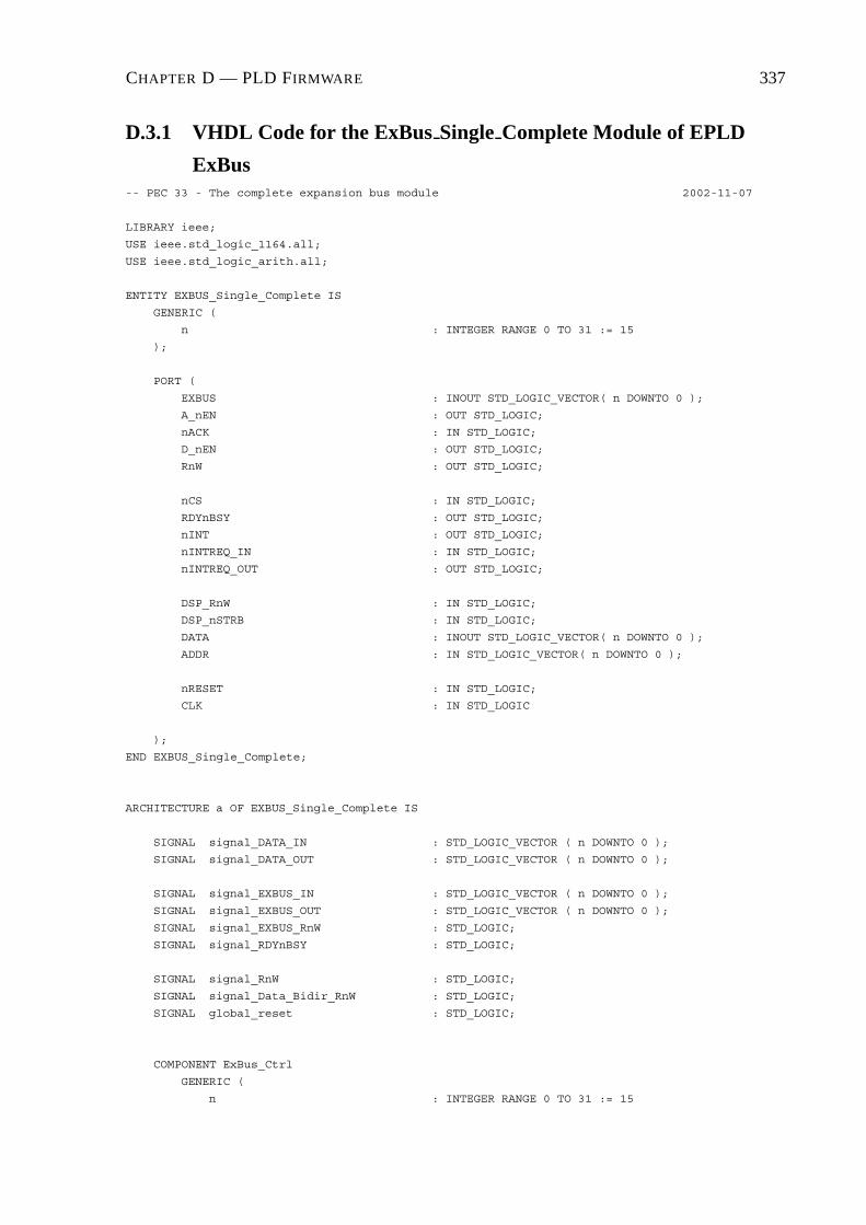
CHAPTER D — PLD FIRMWARE 337
D.3.1 VHDL Code for the ExBus Single Complete Module of EPLD
ExBus-- PEC 33 - The complete expansion bus module 2002-11-07
LIBRARY ieee;
USE ieee.std_logic_1164.all;
USE ieee.std_logic_arith.all;
ENTITY EXBUS_Single_Complete IS
GENERIC (
n : INTEGER RANGE 0 TO 31 := 15
);
PORT (
EXBUS : INOUT STD_LOGIC_VECTOR( n DOWNTO 0 );
A_nEN : OUT STD_LOGIC;
nACK : IN STD_LOGIC;
D_nEN : OUT STD_LOGIC;
RnW : OUT STD_LOGIC;
nCS : IN STD_LOGIC;
RDYnBSY : OUT STD_LOGIC;
nINT : OUT STD_LOGIC;
nINTREQ_IN : IN STD_LOGIC;
nINTREQ_OUT : OUT STD_LOGIC;
DSP_RnW : IN STD_LOGIC;
DSP_nSTRB : IN STD_LOGIC;
DATA : INOUT STD_LOGIC_VECTOR( n DOWNTO 0 );
ADDR : IN STD_LOGIC_VECTOR( n DOWNTO 0 );
nRESET : IN STD_LOGIC;
CLK : IN STD_LOGIC
);
END EXBUS_Single_Complete;
ARCHITECTURE a OF EXBUS_Single_Complete IS
SIGNAL signal_DATA_IN : STD_LOGIC_VECTOR ( n DOWNTO 0 );
SIGNAL signal_DATA_OUT : STD_LOGIC_VECTOR ( n DOWNTO 0 );
SIGNAL signal_EXBUS_IN : STD_LOGIC_VECTOR ( n DOWNTO 0 );
SIGNAL signal_EXBUS_OUT : STD_LOGIC_VECTOR ( n DOWNTO 0 );
SIGNAL signal_EXBUS_RnW : STD_LOGIC;
SIGNAL signal_RDYnBSY : STD_LOGIC;
SIGNAL signal_RnW : STD_LOGIC;
SIGNAL signal_Data_Bidir_RnW : STD_LOGIC;
SIGNAL global_reset : STD_LOGIC;
COMPONENT ExBus_Ctrl
GENERIC (
n : INTEGER RANGE 0 TO 31 := 15
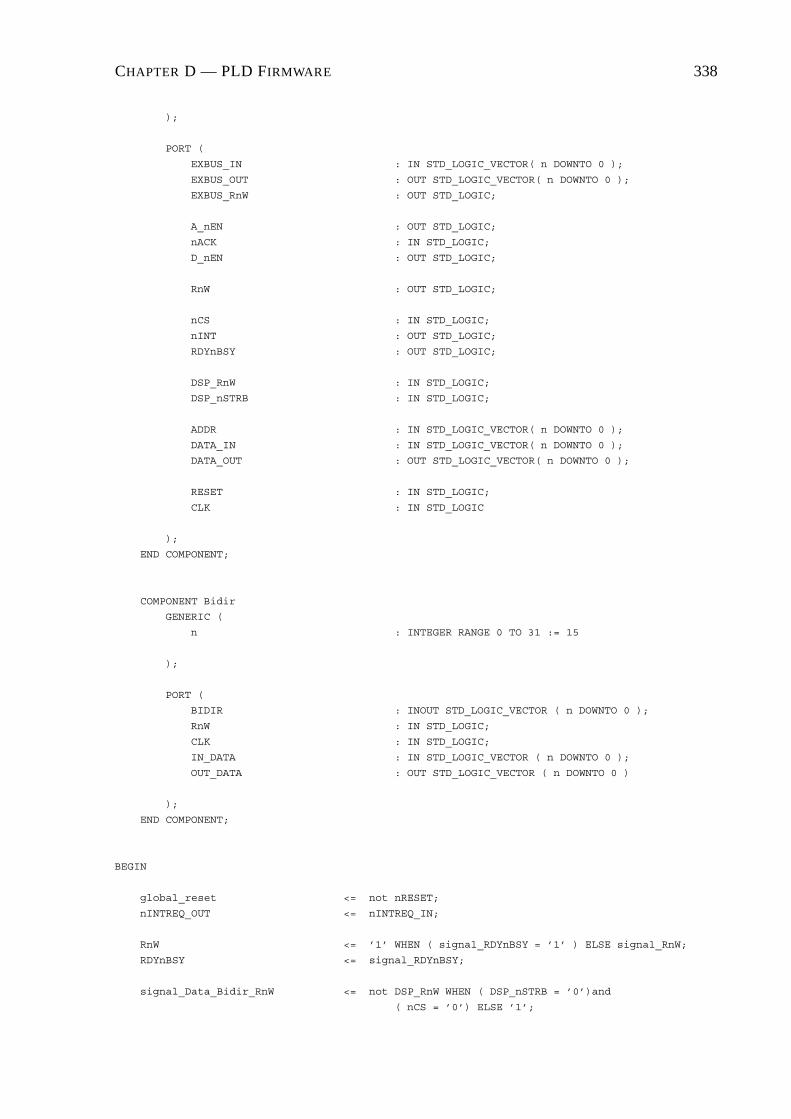
CHAPTER D — PLD FIRMWARE 338
);
PORT (
EXBUS_IN : IN STD_LOGIC_VECTOR( n DOWNTO 0 );
EXBUS_OUT : OUT STD_LOGIC_VECTOR( n DOWNTO 0 );
EXBUS_RnW : OUT STD_LOGIC;
A_nEN : OUT STD_LOGIC;
nACK : IN STD_LOGIC;
D_nEN : OUT STD_LOGIC;
RnW : OUT STD_LOGIC;
nCS : IN STD_LOGIC;
nINT : OUT STD_LOGIC;
RDYnBSY : OUT STD_LOGIC;
DSP_RnW : IN STD_LOGIC;
DSP_nSTRB : IN STD_LOGIC;
ADDR : IN STD_LOGIC_VECTOR( n DOWNTO 0 );
DATA_IN : IN STD_LOGIC_VECTOR( n DOWNTO 0 );
DATA_OUT : OUT STD_LOGIC_VECTOR( n DOWNTO 0 );
RESET : IN STD_LOGIC;
CLK : IN STD_LOGIC
);
END COMPONENT;
COMPONENT Bidir
GENERIC (
n : INTEGER RANGE 0 TO 31 := 15
);
PORT (
BIDIR : INOUT STD_LOGIC_VECTOR ( n DOWNTO 0 );
RnW : IN STD_LOGIC;
CLK : IN STD_LOGIC;
IN_DATA : IN STD_LOGIC_VECTOR ( n DOWNTO 0 );
OUT_DATA : OUT STD_LOGIC_VECTOR ( n DOWNTO 0 )
);
END COMPONENT;
BEGIN
global_reset <= not nRESET;
nINTREQ_OUT <= nINTREQ_IN;
RnW <= ’1’ WHEN ( signal_RDYnBSY = ’1’ ) ELSE signal_RnW;
RDYnBSY <= signal_RDYnBSY;
signal_Data_Bidir_RnW <= not DSP_RnW WHEN ( DSP_nSTRB = ’0’)and
( nCS = ’0’) ELSE ’1’;
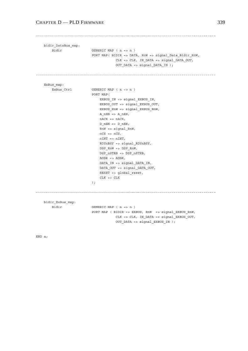
CHAPTER D — PLD FIRMWARE 339
------------------------------------------------------------------------------------------
bidir_DataBus_map:
Bidir GENERIC MAP ( n => n )
PORT MAP( BIDIR => DATA, RnW => signal_Data_Bidir_RnW,
CLK => CLK, IN_DATA => signal_DATA_OUT,
OUT_DATA => signal_DATA_IN );
------------------------------------------------------------------------------------------
ExBus_map:
ExBus_Ctrl GENERIC MAP ( n => n )
PORT MAP(
EXBUS_IN => signal_EXBUS_IN,
EXBUS_OUT => signal_EXBUS_OUT,
EXBUS_RnW => signal_EXBUS_RnW,
A_nEN => A_nEN,
nACK => nACK,
D_nEN => D_nEN,
RnW => signal_RnW,
nCS => nCS,
nINT => nINT,
RDYnBSY => signal_RDYnBSY,
DSP_RnW => DSP_RnW,
DSP_nSTRB => DSP_nSTRB,
ADDR => ADDR,
DATA_IN => signal_DATA_IN,
DATA_OUT => signal_DATA_OUT,
RESET => global_reset,
CLK => CLK
);
------------------------------------------------------------------------------------------
bidir_ExBus_map:
Bidir GENERIC MAP ( n => n )
PORT MAP ( BIDIR => EXBUS, RnW => signal_EXBUS_RnW,
CLK => CLK, IN_DATA => signal_EXBUS_OUT,
OUT_DATA => signal_EXBUS_IN );
END a;

CHAPTER D — PLD FIRMWARE 340

CHAPTER D — PLD FIRMWARE 341
D.3.2 VHDL Code for the ExBus Ctrl Module of EPLD ExBus-- PEC 33 - Expansion Bus Component 2002-11-01
LIBRARY ieee;
USE ieee.std_logic_1164.all;
USE ieee.std_logic_arith.all;
ENTITY EXBUS_Ctrl IS
GENERIC (
n : INTEGER RANGE 0 TO 31 := 15
);
PORT (
EXBUS_IN : IN STD_LOGIC_VECTOR( n DOWNTO 0 );
EXBUS_OUT : OUT STD_LOGIC_VECTOR( n DOWNTO 0 );
EXBUS_RnW : OUT STD_LOGIC;
A_nEN : OUT STD_LOGIC;
nACK : IN STD_LOGIC;
D_nEN : OUT STD_LOGIC;
RnW : OUT STD_LOGIC; --Next transaction type
nCS : IN STD_LOGIC;
nINT : OUT STD_LOGIC;
RDYnBSY : OUT STD_LOGIC;
DSP_RnW : IN STD_LOGIC;
DSP_nSTRB : IN STD_LOGIC;
ADDR : IN STD_LOGIC_VECTOR( n DOWNTO 0 );
DATA_IN : IN STD_LOGIC_VECTOR( n DOWNTO 0 );
DATA_OUT : OUT STD_LOGIC_VECTOR( n DOWNTO 0 );
RESET : IN STD_LOGIC;
CLK : IN STD_LOGIC
);
END EXBUS_Ctrl;
ARCHITECTURE a OF EXBUS_Ctrl IS
TYPE state_type IS ( idle_state, addr_state, addr_ack_state, data_state,
data_ack_state, nint_state );
SIGNAL state : state_type;
SIGNAL next_state : state_type;
SIGNAL signal_DATA_OUT : STD_LOGIC_VECTOR ( n DOWNTO 0 );
SIGNAL signal_DATA_IN : STD_LOGIC_VECTOR ( n DOWNTO 0 );
SIGNAL signal_EXBUS_OUT : STD_LOGIC_VECTOR ( n DOWNTO 0 );
SIGNAL signal_EXBUS_IN : STD_LOGIC_VECTOR ( n DOWNTO 0 );
SIGNAL signal_WR_DATA : STD_LOGIC_VECTOR ( n DOWNTO 0 );
SIGNAL signal_RD_DATA : STD_LOGIC_VECTOR ( n DOWNTO 0 );
SIGNAL signal_ADDR : STD_LOGIC_VECTOR ( n DOWNTO 0 );

CHAPTER D — PLD FIRMWARE 342
-- RnW signal for Expansion Bus ( == NOT RnW for Data Bus )
SIGNAL signal_RnW : STD_LOGIC;
SIGNAL signal_RDYnBSY : STD_LOGIC;
SIGNAL clk_cntr : INTEGER RANGE 0 TO 15;
SIGNAL addr_ack_rec : STD_LOGIC;
SIGNAL data_ack_rec : STD_LOGIC;
SIGNAL start_trig : STD_LOGIC;
BEGIN
A_nEN <= ’0’ WHEN ( state = addr_state ) ELSE ’1’;
D_nEN <= ’0’ WHEN ( state = data_state ) ELSE ’1’;
nINT <= ’0’ WHEN ( state = nint_state ) ELSE ’1’;
RDYnBSY <= signal_RDYnBSY;
signal_RDYnBSY <= ’1’ WHEN ( state = idle_state ) ELSE ’0’;
DATA_OUT <= signal_DATA_OUT;
signal_DATA_IN <= DATA_IN;
signal_EXBUS_IN <= EXBUS_IN;
RnW <= signal_RnW;
------------------------------------------------------------------------------------------
EXBUS_RnW_proc:
PROCESS ( CLK, RESET )
BEGIN
IF ( RESET = ’1’ ) THEN
EXBUS_RnW <= ’1’;
ELSIF ( CLK’event )and( CLK = ’1’ ) THEN
IF ( state = idle_state ) THEN
EXBUS_RnW <= ’1’;
ELSIF ( state = addr_state)or( state = addr_ack_state ) THEN
EXBUS_RnW <= ’0’;
ELSE
EXBUS_RnW <= signal_RnW;
END IF;
END IF;
END PROCESS EXBUS_RnW_proc;
------------------------------------------------------------------------------------------
ADDR_proc:
PROCESS ( DSP_nSTRB, RESET )
BEGIN
IF ( RESET = ’1’ ) THEN
signal_ADDR <= ( others => ’0’ );

CHAPTER D — PLD FIRMWARE 343
ELSIF ( DSP_nSTRB’event )and( DSP_nSTRB = ’0’ ) THEN
IF ( nCS = ’0’ )and( state = idle_state ) THEN
signal_ADDR <= ADDR;
ELSE
signal_ADDR <= signal_ADDR;
END IF;
END IF;
END PROCESS ADDR_proc;
------------------------------------------------------------------------------------------
WR_DATA_proc:
PROCESS ( DSP_nSTRB, RESET )
BEGIN
IF ( RESET = ’1’ ) THEN
signal_WR_DATA <= ( others => ’0’ );
ELSIF ( DSP_nSTRB’event )and( DSP_nSTRB = ’1’ ) THEN
IF ( nCS = ’0’ )and( state = idle_state )and( signal_RnW = ’0’ ) THEN
signal_WR_DATA <= signal_DATA_IN;
ELSE
signal_WR_DATA <= signal_WR_DATA;
END IF;
END IF;
END PROCESS WR_DATA_proc;
------------------------------------------------------------------------------------------
DATA_OUT_proc:
PROCESS ( DSP_nSTRB, RESET )
BEGIN
IF ( RESET = ’1’ ) THEN
signal_DATA_OUT <= ( others => ’0’ );
ELSIF ( DSP_nSTRB’event )and( DSP_nSTRB = ’0’ ) THEN
IF ( nCS = ’0’ )and( state = idle_state ) THEN
signal_DATA_OUT <= signal_RD_DATA;
ELSE
signal_DATA_OUT <= signal_DATA_OUT;
END IF;
END IF;
END PROCESS DATA_OUT_proc;
------------------------------------------------------------------------------------------
signal_RnW_proc:
PROCESS ( DSP_nSTRB, RESET )
CHAPTER D — PLD FIRMWARE 344
BEGIN
IF ( RESET = ’1’ ) THEN
signal_RnW <= ’1’;
ELSIF ( DSP_nSTRB’event )and( DSP_nSTRB = ’0’ ) THEN
IF ( nCS = ’0’ )and( state = idle_state ) THEN
signal_RnW <= DSP_RnW;
ELSE
signal_RnW <= signal_RnW;
END IF;
END IF;
END PROCESS signal_RnW_proc;
------------------------------------------------------------------------------------------
EXBUS_OUT_proc:
PROCESS ( CLK, RESET )
BEGIN
IF ( RESET = ’1’ ) THEN
EXBUS_OUT <= ( others => ’0’ );
ELSIF ( CLK’event )and( CLK = ’1’ ) THEN
IF ( state = addr_state ) THEN
EXBUS_OUT <= signal_ADDR;
ELSIF ( state = data_state )or( state = data_ack_state ) THEN
EXBUS_OUT <= signal_WR_DATA;
END IF;
END IF;
END PROCESS EXBUS_OUT_proc;
------------------------------------------------------------------------------------------
EXBUS_IN_proc:
PROCESS ( nACK, RESET, state )
BEGIN
IF ( RESET = ’1’ ) THEN
signal_RD_DATA <= ( others => ’0’ );
ELSIF ( nACK’event )and( nACK = ’0’ ) THEN
IF ( ( state = data_ack_state )or( state = data_ack_state ) )and
( signal_RnW = ’1’ ) THEN
signal_RD_DATA <= signal_EXBUS_IN;
ELSE
signal_RD_DATA <= signal_RD_DATA;
END IF;
END IF;
END PROCESS EXBUS_IN_proc;

CHAPTER D — PLD FIRMWARE 345
------------------------------------------------------------------------------------------
addr_ack_proc:
PROCESS ( nACK, RESET )
BEGIN
IF ( RESET = ’1’ )or( state /= addr_ack_state ) THEN
addr_ack_rec <= ’0’;
ELSIF ( nACK’event )and( nACK = ’0’ ) THEN
addr_ack_rec <= ’1’;
END IF;
END PROCESS addr_ack_proc;
------------------------------------------------------------------------------------------
data_ack_proc:
PROCESS ( nACK, RESET )
BEGIN
IF ( RESET = ’1’ )or( state /= data_ack_state ) THEN
data_ack_rec <= ’0’;
ELSIF ( nACK’event )and( nACK = ’0’ ) THEN
data_ack_rec <= ’1’;
END IF;
END PROCESS data_ack_proc;
------------------------------------------------------------------------------------------
sm_proc:
PROCESS ( state )
BEGIN
CASE state IS
WHEN idle_state =>
next_state <= addr_state;
WHEN addr_state =>
next_state <= addr_ack_state;
WHEN addr_ack_state =>
IF ( addr_ack_rec = ’1’ ) THEN
next_state <= data_state;
ELSE
next_state <= idle_state;
END IF;
WHEN data_state =>
next_state <= data_ack_state;
WHEN data_ack_state =>
IF ( signal_RnW = ’1’ ) THEN
next_state <= nint_state;

CHAPTER D — PLD FIRMWARE 346
ELSE
next_state <= idle_state;
END IF;
WHEN nint_state =>
next_state <= idle_state;
END CASE;
END PROCESS sm_proc;
------------------------------------------------------------------------------------------
sm_ctrl_proc:
PROCESS ( CLK, RESET )
BEGIN
IF ( RESET = ’1’ ) THEN
state <= idle_state;
clk_cntr <= 0;
ELSIF ( CLK’event )and( CLK = ’1’ ) THEN
IF ( start_trig = ’1’ ) THEN
state <= addr_state;
clk_cntr <= 0;
ELSIF ( ( addr_ack_rec = ’1’ )or( clk_cntr = 14 ) )and
( state = addr_ack_state ) THEN
state <= data_state;
clk_cntr <= 0;
ELSIF ( ( data_ack_rec = ’1’ )or( clk_cntr = 14 ) )and
( state = data_ack_state ) THEN
state <= next_state;
clk_cntr <= 0;
ELSIF ( clk_cntr = 4 )and( ( state = data_state )or
( state = addr_state ) ) THEN
state <= next_state;
clk_cntr <= 0;
ELSIF ( clk_cntr = 1 )and( state = nint_state ) THEN
state <= next_state;
clk_cntr <= 0;
ELSIF ( state /= idle_state ) THEN
state <= state;
clk_cntr <= clk_cntr + 1;
ELSE
state <= state;
clk_cntr <= clk_cntr;
END IF;
END IF;
END PROCESS sm_ctrl_proc;

CHAPTER D — PLD FIRMWARE 347
------------------------------------------------------------------------------------------
start_proc:
PROCESS ( DSP_nSTRB, RESET )
BEGIN
IF ( RESET = ’1’ )or( signal_RDYnBSY = ’0’ ) THEN
start_trig <= ’0’;
ELSIF ( DSP_nSTRB’event )and( DSP_nSTRB = ’1’ ) THEN
IF ( nCS = ’0’ ) THEN
start_trig <= ’1’;
END IF;
END IF;
END PROCESS start_proc;
END a;

CHAPTER D — PLD FIRMWARE 348
D.3.3 VHDL Code for the BiDir Module of EPLD ExBus-- Bidirectional Bus 2002-11-07
LIBRARY ieee;
USE ieee.std_logic_1164.all;
USE ieee.std_logic_arith.all;
-- -------------------------------------------------------------------
-- | RnW | BIDIR | IN_DATA | OUT_DATA |
-- -------------------------------------------------------------------
-- -------------------------------------------------------------------
-- | 1 | ZZZZZZZZZZZZZZZZ | XXXXXXXXXXXXXXXX | BIDIR |
-- -------------------------------------------------------------------
-- | 0 | IN_DATA | Data | BIDIR |
-- -------------------------------------------------------------------
ENTITY Bidir IS
GENERIC (
n : INTEGER RANGE 0 TO 31 := 15
);
PORT (
BIDIR : INOUT STD_LOGIC_VECTOR ( n DOWNTO 0 );
RnW : IN STD_LOGIC;
CLK : IN STD_LOGIC;
IN_DATA : IN STD_LOGIC_VECTOR ( n DOWNTO 0 );
OUT_DATA : OUT STD_LOGIC_VECTOR ( n DOWNTO 0 )
);
END Bidir;
ARCHITECTURE maxpld OF Bidir IS
SIGNAL a : STD_LOGIC_VECTOR ( n DOWNTO 0 );
SIGNAL b : STD_LOGIC_VECTOR ( n DOWNTO 0 );
BEGIN
PROCESS ( CLK )
BEGIN
IF ( CLK’event )and( CLK = ’0’ ) THEN
a <= IN_DATA;
OUT_DATA <= b;
END IF;
END PROCESS;
PROCESS ( RnW, BIDIR )
BEGIN
IF ( RnW = ’1’ ) THEN
BIDIR <= ( others => ’Z’ );
b <= BIDIR;
ELSE
BIDIR <= a;

CHAPTER D — PLD FIRMWARE 349
b <= BIDIR;
END IF;
END PROCESS;
END maxpld;