design and implementation of a probe station as capstone
TRANSCRIPT
2006-907: DESIGN AND IMPLEMENTATION OF A PROBE STATION ASCAPSTONE PROJECT
Lihong (Heidi) Jiao, Grand Valley State UniversityLihong (Heidi) Jiao,Ph.D., is an Assistant Professor in the Padnos College of Engineering andComputing at Grand Valley State University. She received her B.S.E.E. and M.S.E.E. fromNankai University, China and Ph.D in Electrical Engineering from the Pennsylvania StateUniversity. Her interests include semiconductor device fabrication, nanotechnologies and fiberoptics.
Jeffrey Ray, Grand Valley State UniversityJeff Ray, Ph.D., is Director of the School of Engineering and an Associate Professor ofEngineering at Grand Valley State University. Dr. Ray holds a BS and MS in MechanicalEngineering from Tennessee Technological University and a Ph.D. from Vanderbilt University.His teaching interests are vibrations, CAD/CAM/CAE, and engineering design. Researchinterests include engineering education pedagogy and use of computer-aided engineeringapplications for design.
© American Society for Engineering Education, 2006
Page 11.397.1
Design and Implementation of a Probe Station as a
Capstone Project
Abstract
A probe station is an essential piece of equipment used in semiconductor wafer testing. It provides a platform for the wafer to interface with the electrical test equipment. During wafer testing, electrical probes are lowered onto the semiconductor wafer and make electrical connections to the wafer. This paper presents the design and implementation of a probe station project that was carried out as a capstone senior design project in School of Engineering at Grand Valley State University. The probe station was designed to have a durable, stable base and a 4 inch vacuum-assisted hot chuck as a sample stage. A microscope was integrated to view the wafers and to assist in making the electrical connections. In addition, microprobes with the
ability to probe the wafers of 25om structure were designed. The project team consisted of students with majors in mechanical and electrical engineering. The students learned skills in team building, project management, communication skills, and budgeting. The outcome of this project was a fully functional probe station currently used in the solid-state laboratory. 1. Introduction
All engineering students in School of Engineering at Grand Valley State University (GVSU) are required to take a multidisciplinary two-course capstone design sequence during their senior year. The two courses are structured to provide all students with a real-world understanding of the practice and principles of engineering and project management. The first course, EGR485 - Senior Engineering Project I, focuses on topics directly related to project management of industry projects including teambuilding, conflict resolution, leadership, resource availability, and design methodologies. In addition, students are assigned to teams and prepare a design proposal and presentation for the industry sponsor. During the second course, EGR 486 - Senior Engineering Project II, teams purchase all raw materials, build and implement their design, and write final documentation for the industry sponsors. Topics covered during the course include:
‚ Understanding the interdependence of teams
‚ Handling difficult situations in executing design projects
‚ Further development of their written and oral communication skills
‚ Developing leadership skills necessary for successful projects
‚ Efficient time management practices
‚ Introduction of project management techniques, including critical path and Gantt chart creation
The electronic materials/devices course in School of Engineering at GVSU has been enhanced with a laboratory component. The challenge for adding laboratory activities to a course like this is the cost of the equipment needed. In order to test the functional properties of integrated circuits in the wafer form, a probe station is essential1. However, commercially available wafer testing probe stations are expensive2,3,4. The proposal “Probe Station Design and Manufacture” was submitted and accepted as a senior capstone project by School of Engineering. The criteria of building the probe station are:
Page 11.397.2

‚ The sample stage must serve as the sample holder and hot plate with a temperature range from room temperature to 300oC.
‚ The sample stage must be able to move in x, y, and z directions.
‚ Wafers up to 4 inch in diameter can be probed.
‚ Microprobes must be connected to external electrical testing instruments through standard BNC connectors.
‚ Microprobes must be able to move in x, y, and z directions.
‚ The samples can be magnified up to 80 times. Designing and building the probe station required knowledge in both mechanical and electrical engineering subject areas. Four mechanical and two electrical engineering students were assigned to the project based on faculty understanding of the project and an application for participating in the senior capstone courses. The purpose of the application is to learn of the skills acquired while the students were participating in their cooperative education program. Other essential information obtained includes major, technical electives taken or planned to take, and strengths and weaknesses. Following project assignment students began the process of learning their team members, assigning roles and responsibilities within the team, meeting with the corporate sponsor, and design proposal development. This gives students an opportunity to gain experiences to be successful in their future careers. Faculty members were used as design consultants throughout the courses. The course coordinator monitors all teams throughout the two semester sequence. This paper presents the process of this senior capstone project. In section 2 the wafer testing probe station is described and the design consideration is discussed in section 3. Sections 4, 5 and 6 cover details in design, manufacturing, and system testing. Budget is considered in section 7. 2. Wafer Testing Probe Station
Integrated circuits on a wafer differ from circuits on a printed board in manufacturing processes. All components of the integrated circuits are deposited on a single semiconductor wafer. The size of the circuits is extremely small. In order to conduct functional testing, precision micromanipulators used to position and hold microprobes, along with a long working distance microscope, are required. These micromanipulators are held on the metallic working platen by magnets. The sample stage/chuck has multiple functions. First, it provides mechanical support to the sample which is secured by the chuck vacuum system. Secondly, it serves as a hot plate with temperature ranging from room temperature to 300oC. Thirdly, the chuck is capable of performing independent x, y, and z motions. To provide stability during wafer testing, the probe station must have a heavy and rugged base. A three dimensional rendering of the probe station is shown in Figure 1. The probe station consists of microscope, precision micromanipulators, working platen, movable sample holder/chuck, and rugged base.
Page 11.397.3

Power/air control Microscope
Micromanipulator
Working platen Sample
stage/chuck
Rugged base
Figure 1. Three-dimensional Rendering of the Probe Station. Specifications of the desired probe station are listed in Table 1.
Table 1. Probe Station Specifications.
Chuck diameter 120mm (5 inches)
Resolution of the micromanipulator 50 nm
X and Y moving range of chuck 50 mm x 100 mm
Z moving range of chuck 50 mm
Temperature range of chuck Room temperature – 300oC
Microscope objective lens 2x, 4x
Microscope eyepiece 20x
Connectors to the external instruments BNC
3. Design Consideration
The probe station has three major functional components: the chuck, micromanipulators, and XYZ chuck movements. 3.1 Chuck
The surface of the chuck needs to conduct electricity. Since gold is one of the best conducting metals available, the chuck can be gold plated using a base material of either low carbon steel or a brass alloy. Both band heater and disc heater can be used to provide temperature for the chuck. To obtain stable, uniform temperature across the surface of the chuck, the heat transfer analysis was conducted to evaluate the difference in thermal uniformity for two types of heaters. Since the
Page 11.397.4

sample under test covers the surface during testing and the air gap between the sample and the chuck is minimal, the heat transfer from convection is negligible. The chuck was assumed to be five inches in diameter fabricated from steel, in addition, the system is assumed to be at steady state. The energy equation was written as:
Â/
??©ij
ji
R
TT
dt
dT0c (1)
Where c is thermal diffusivity, T is temperature, and Rij is the thermal resistance between node i and node j. To obtain the temperature distribution using equation 1, Rij which is different for different structured heater needed to be determined first. The numerical mesh method was used to analyze the thermal resistance. The thermal resistance between any two nodes was derived using equation 2.
kA
xRij
F? (2)
Where Fx is the distance between node i and node j, k is the thermal conductivity, and A is the cross sectional area through which heat transfer is conducted. From equations (2) and (1), temperature distribution for both types of heaters was calculated. Figure 2a shows the band heater temperature mesh and Figure 2b shows the disc heater temperature mesh, which were used to calculate the temperature difference between outside edge and the center. It was found that T1, T2 and T3 are 112.5oC, 225oC and 225oC respectively for the band heater structure. T1, T2 and T3 are 300oC, 300oC and 300oC respectively for the disc heater structure. From the above calculation, it can be seen that the disc heater would provide a much more uniform heat transfer across the surface of the chuck.
Figure 2a. Band Heater Temperature Mesh. Figure 2b. Disc Heater Temperature Mesh.
Page 11.397.5

To securely hold the sample on the chuck, vacuum is provided through the center hole. Figure 3 illustrates the forces applied on the sample with the vacuum system engaged.
The force applied on the sample can be obtained by equation 3.
APF vacuumvacuum ? (3)
Where Fvacuum is the vacuum force on the sample, Pvacuum is the vacuum pressure and A is the area of the hole. Since the sample size is bigger than the size of the hole, the force applied on to the outside of the sample needs to know and can be related to the vacuum pressure through equation 4.
appliedvacuum FF 2? (4)
From equations 3 and 4, it can be seen that with 12.3 psi of vacuum pressure and 0.049 in2 of hole, the force applied on to the edge of the sample is 0.3 lbs which is high enough to hold the 4 inch wafer. 3.2 X, Y, and Z chuck movement
Considering the factors of ability to manufacturing and cost, commercially available XY table can be purchased and incorporated with the in-house built Z axis. The Z-movement can be conducted by using a scissor jack assembly. 3.3 Micromanipulators
The micromanipulator needs to provide high precision probing. This can be satisfied by using linear x and y direction movements. To better control z direction, rotational movement can be used. 4. Design
Sample
Fapplied
Pvacuum
Figure 3. Forces Applied on the Sample by the Vacuum.
Page 11.397.6

4.1 Chuck and XYZ movements
Figure 4 shows the design of the chuck and XYZ movement assembly. The chuck has a hole in the center to accommodate the vacuum system. A metal pipe connects the hole directly to a vacuum generator that creates vacuum using pressurized air. A disc heater connected to the temperature controller provides the chuck with the desired temperature. The surface of the chuck is gold plated to increase the electric conductivity. The chuck assembly is connected to the Z axis assembly. Rotating the screw moves the chuck up or down. The XY table is connected to Z axis assembly to enable the movements in X and Y direction.
Chuck
Disc heater
Ceramic disc
Z - axis
XY table
Figure 4. Chuck and XYZ Movement Assembly. 4.2 Micromanipulator
The micromanipulator has an assembly of three main blocks. The middle block moves in x-direction on a machined track relative to the bottom block controlled by the threaded rod. The third block that sits on top of the middle block moves in y-direction. The rotating arm moving in z direction is controlled by a screw. Figure 5a shows the design of the micromanipulator assembly and Figure 5b shows the expanded view of the micromanipulator assembly.
Page 11.397.7
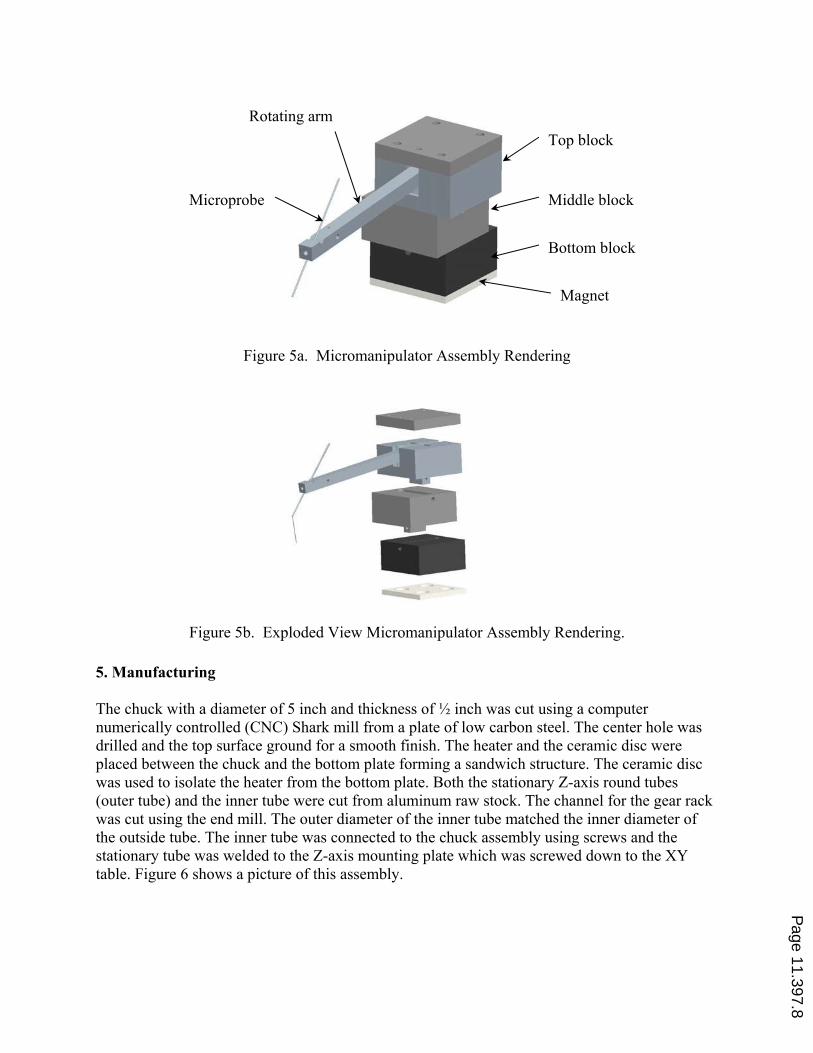
Rotating arm
Top block
Microprobe Middle block
Bottom block
Magnet
Figure 5a. Micromanipulator Assembly Rendering
Figure 5b. Exploded View Micromanipulator Assembly Rendering.
5. Manufacturing
The chuck with a diameter of 5 inch and thickness of ½ inch was cut using a computer numerically controlled (CNC) Shark mill from a plate of low carbon steel. The center hole was drilled and the top surface ground for a smooth finish. The heater and the ceramic disc were placed between the chuck and the bottom plate forming a sandwich structure. The ceramic disc was used to isolate the heater from the bottom plate. Both the stationary Z-axis round tubes (outer tube) and the inner tube were cut from aluminum raw stock. The channel for the gear rack was cut using the end mill. The outer diameter of the inner tube matched the inner diameter of the outside tube. The inner tube was connected to the chuck assembly using screws and the stationary tube was welded to the Z-axis mounting plate which was screwed down to the XY table. Figure 6 shows a picture of this assembly.
Page 11.397.8
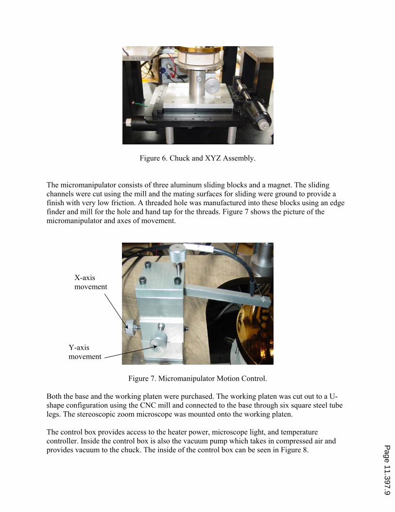
Figure 6. Chuck and XYZ Assembly.
The micromanipulator consists of three aluminum sliding blocks and a magnet. The sliding channels were cut using the mill and the mating surfaces for sliding were ground to provide a finish with very low friction. A threaded hole was manufactured into these blocks using an edge finder and mill for the hole and hand tap for the threads. Figure 7 shows the picture of the micromanipulator and axes of movement.
X-axis movement
Y-axis movement
Figure 7. Micromanipulator Motion Control.
Both the base and the working platen were purchased. The working platen was cut out to a U-shape configuration using the CNC mill and connected to the base through six square steel tube legs. The stereoscopic zoom microscope was mounted onto the working platen. The control box provides access to the heater power, microscope light, and temperature controller. Inside the control box is also the vacuum pump which takes in compressed air and provides vacuum to the chuck. The inside of the control box can be seen in Figure 8.
Page 11.397.9

Figure 8. Interior View of the Control Box.
6. System testing and results
The outcome of this senior capstone project is the wafer testing probe station shown in Figure 9 below. The performance testing was conducted to certify that the probe station met the design requirements. The probe station was subjected to a series of tests for the various functions of the device.
Figure 9. Photo of Wafer Testing Probe Station.
The electrical functionality of the microprobes was tested. The resistance between the BNC connector and the probe tip was less than 2 ohms. The vacuum system was also tested with a
Page 11.397.10
small wafer sample and a large sample. At both room temperature and 300oC, there was no movement of the sample (seen with microscope) when the probe tip was applied. The testing of the performance of the heater was also conducted. There was a 5oC maximum temperature difference between the edge and center of the chuck. One of the important design criteria is the resolution of the micromanipulator. Using the testing wafer which consisted of two lines spaced by 50nm, the micromanipulators were tested and the resolution was 50nm which met the design requirement. 7. Budget
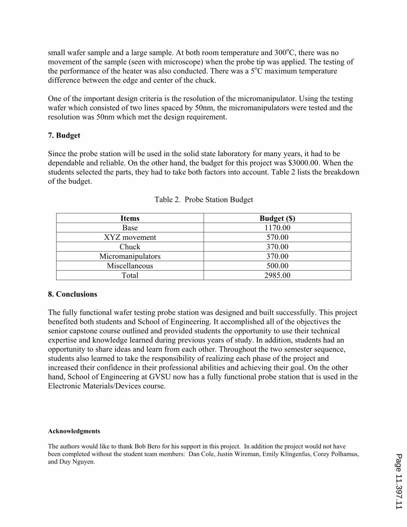
Since the probe station will be used in the solid state laboratory for many years, it had to be dependable and reliable. On the other hand, the budget for this project was $3000.00. When the students selected the parts, they had to take both factors into account. Table 2 lists the breakdown of the budget.
Table 2. Probe Station Budget
Items Budget ($)
Base 1170.00
XYZ movement 570.00
Chuck 370.00
Micromanipulators 370.00
Miscellaneous 500.00
Total 2985.00
8. Conclusions
The fully functional wafer testing probe station was designed and built successfully. This project benefited both students and School of Engineering. It accomplished all of the objectives the senior capstone course outlined and provided students the opportunity to use their technical expertise and knowledge learned during previous years of study. In addition, students had an opportunity to share ideas and learn from each other. Throughout the two semester sequence, students also learned to take the responsibility of realizing each phase of the project and increased their confidence in their professional abilities and achieving their goal. On the other hand, School of Engineering at GVSU now has a fully functional probe station that is used in the Electronic Materials/Devices course. Acknowledgments
The authors would like to thank Bob Bero for his support in this project. In addition the project would not have been completed without the student team members: Dan Cole, Justin Wireman, Emily Klingenfus, Corey Polhamus, and Duy Nguyen.
Page 11.397.11

Bibliography
1. Micromanipulator, “Basics of Low Current Probing”, application note #A1009492. 2. Micromanipulator, “High Performance Thermal Chuck System”. 3. K. F. Hollman and D. L. Harrison, “Wafer probe station”, U.S. Patent 6,803,756, 2004. 4. P. Navratil, B. Froemke, C. Stewart, A. Lord, Spencer, S. Runbaugh, G. Fisher, P. McCann, and T. Jones,
“Probe station”, U.S. Patent 6,777,964, 2004.
Page 11.397.12