design and implementation of an asynchronous version of
TRANSCRIPT

Rochester Institute of Technology Rochester Institute of Technology
RIT Scholar Works RIT Scholar Works
Theses
11-1-1993
Design and implementation of an asynchronous version of the Design and implementation of an asynchronous version of the
MIPS R3000 microprocessor MIPS R3000 microprocessor
Scott Siers
Follow this and additional works at: https://scholarworks.rit.edu/theses
Recommended Citation Recommended Citation Siers, Scott, "Design and implementation of an asynchronous version of the MIPS R3000 microprocessor" (1993). Thesis. Rochester Institute of Technology. Accessed from
This Thesis is brought to you for free and open access by RIT Scholar Works. It has been accepted for inclusion in Theses by an authorized administrator of RIT Scholar Works. For more information, please contact [email protected].
DESIGN AND IMPLEMENTATION OF ANASYNCHRONOUS VERSION OF THE MIPS
R3000 MICROPROCESSOR
by
Scott Siers
A Thesis Submittedill
Partial Fulfillment of theRequirements for the Degree of
MASTER OF SCIENCEill
Computer Engineering
Approved by:
Graduate Advisor - George A. Brown, Professor
Roy S. Czernikowski, Professor and Department Head
Tony H. Chang, Professor
Department of Computer EngineeringCollege of Engineering
Rochester Institute of TechnologyRochester, New York
November, 1993

ABSTRACT
The goal of this thesis is to demonstrate the feasibility of converting a synchronous general
purpose microprocessor design to one using an asynchronous methodology. This thesis is
one of three parts that details the entire design of an asynchronous version of the MIPS
R3000 microprocessor. The design excludes all of the memory support features of the
processor for two reasons. First, the memory is already handled asynchronously and
second, the size of the project must be limited. This design has implemented the entire set
of instructions from the original synchronous version with the exception of certain
memory instructions. The three participants in this project are Paul Fanelli, Kevin
Johnson, and Scott Siers. Paul Fanelli has developed a Very High Speed Integrated
Circuit Hardware Description Language (VHDL) model for the processor. Kevin Johnson
has designed the register bank, arithmetic logic unit, and shifter, including schematic
diagrams and layouts. Scott Siers has designed the pipeline stages, the multiplier/divider,
the exception handler, and the completion signal generator, including schematic diagrams
and layout. Each of the participants has written a separate thesis that covers one part of
the total design.

Table of Contents
Abstract 1
Table of Contents iii
List of Figures iv
List ofTables vi
Glossary of Terms vii
1 Overview ]
1.1 Design Methodology 2
2 Handshaking in Asynchronous Design 10
2.1 Creation of a Reliable Completion Signal : 1 1
2.2 Handshaking Control Circuit 13
3 Pipeline Structure 20
3.1 Instruction Fetch Stage 23
3.2 Instruction Decode Stage 27
3.2.1 Decoding 27
3.2.1 Address Adder/Incrementer 32
3.2.3 Data Dependencies 35
3.3 Arithmetic Logic Unit Stage 38
3.3.1 Multiplier/Divider Unit 43
3.3.2 Add8 Unit 55
3.4 Memory Stage 58
3.5 Writeback Stage 66
4 Bus Control Unit 71
5 Conclusions 77
6 Bibliography 81
Appendix A List of Instructions A-l
Appendix B Various Files Used in the Project B-l
Appendix C Schematic Diagrams of some Cells Used C-l
Appendix D Layouts of Some Cells Used D-l
m

List of Figures
Figure 1.1 Block Diagram of the Entire Machine 4
Figure 1.2 Calculation of the width of a serpentined transistor 8
Figure 2.1 Basic DCVSL logic module with a reliable completion signal circuit 12
Figure 2.2 State Diagram for a DCVSL Logic Block 13
Figure 2.3 Schematic Diagram for the HCC 15
Figure 2.4 Circuit used to test the HCC 17
Figure 2.5 Timing Diagram of the Handshaking Controller Circuit 1 8
Figure 2.6 Layout of the Handshaking Controller Circuit 19
Figure 3.1 The five stages of the pipeline 21
Figure 3.2 Illustration of Parallel Nature of a Pipelined Machine 21
Figure 3.3 Example showing the advantage of a pipelined machine 22
Figure 3.4 Schematic Diagram of the Instruction Fetch Stage 25
Figure 3.5 Waveforms showing the operation of the IF Stage 26
Figure 3.6 Schematic Diagram of the Instruction Decoder Stage 28
Figure 3.7 Schematic Diagram of the Decoder in the ID Stage 33
Figure 3.8 Schematic Diagram of BJBOX 36
Figure 3.9 Schematic Diagram of the DBOX Unit 39
Figure 3. 10 Schematic Diagram of the TRDS Unit 40
Figure 3.1 1 Schematic Diagram of the Multiplier/Divider Unit 41
Figure 3.12 Block Diagram of the Multiplier/Divider Unit 42
Figure 3.13 Example showing how Booth's algorithm works 47
Figure 3.14 Pseudocode for the Multiplication and Division Algorithms 49
Figure 3.15 State Diagram for the Multiplier 50
Figure 3.16 Schematic Diagram of the Multiplier/Divider Controller 51
Figure 3.17 Connection Pattern for a 8 bitCSA 54
Figure 3.18 Schematic Diagram of the Memory Stage 57
Figure 3. 19 Interface to the Memory Controller 59
Figure 3.20 Schematic Diagram of the Mask Unit 60
Figure 3.21 Schematic Diagram of the Shift Unit 61
Figure 3.22 Example showing how LWL and LWR operate 62
Figure 3.23 Schematic Diagram of the Memory Decoder 63
Figure 3.24 How the VBT corresponds to the bytes in the Register 65
Figure 3.25 Schematic Diagram of the Writeback Stage 68
Figure 3.26 Schematic Diagram of the Writeback Decoder 70
Figure 3.27 Floorplan of the entire processor 70
Figure 4. 1 Schematic Diagram of the Bus Control Unit 73
Figure 4.2 Timing Diagram between the IF stage and the BCU 74
Figure 4.3 States Used in the Bus Control Finite State Machine 75
Figure 4.4 Schematic Diagram of the Bus Control Finite State Machine 76
Figure A.l Complete List of Instructions Implemented A-l
Figure A.2 Decoding scheme used for the instructionsA-2
Figure C. 1 Schematic Diagram of the Tri Stae Buffer C-2
Figure C.2 Schematic Diagram of the SR Latch C-3
IV

Figure C.3 Schematic Diagram of the D Flip-flop C-4
Figure C.4 Schemaitc Diagram of the Conditional Cell C-5
Figure C.5 Schematic Diagram of the Latch C-6
Figure C-6 Schematic Diagram of the Buffer Driver C-7
Figure D.l Layout of the Tri Stae Buffer D-2
Figure D.2 Layout of the SR Latch D-3
Figure D.3 Layout of the D Flip-flop D-4
Figure D.4 Layout of the Conditional Cell D-5
Figure D.5 Layout of the Latch D-6
Figure D-6 Layout of the Buffer Driver D-7

List ofTables
Table 2.1 Definitions of the Signals in the HCC Circuit 15
Table 3.1 Truth Table to determine the destination register 31
Table 3.2 Truth Table for scanning a two bit block 46
Table 3.3 Truth Table for the Modified Booth's Algorithm 47
Table 3.4 Steps for an example using the modified Booth's algorithm 47
Table 3.5 Truth Table to determine operation in a register 53
Table 3.6 VBT Results in Various Cases 65
Table 3.7 Bit Encoding Scheme used to determine the destination register 68
VI
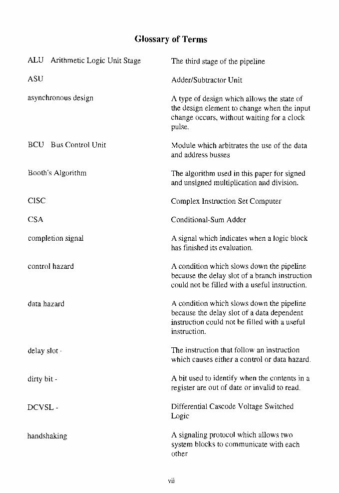
Glossary of Terms
ALU Arithmetic Logic Unit Stage
ASU
asynchronous design
BCU Bus Control Unit
Booth's Algorithm
CISC
CSA
completion signal
control hazard
data hazard
delay slot-
dirty bit -
DCVSL -
handshaking
The third stage of the pipeline
Adder/Subtractor Unit
A type of design which allows the state of
the design element to change when the input
change occurs, without waiting for a clock
pulse.
Module which arbitrates the use of the data
and address busses
The algorithm used in this paper for signed
and unsigned multiplication and division.
Complex Instruction Set Computer
Conditional-Sum Adder
A signal which indicates when a logic block
has finished its evaluation.
A condition which slows down the pipeline
because the delay slot of a branch instruction
could not be filled with a useful instruction.
A condition which slows down the pipeline
because the delay slot of a data dependent
instruction could not be filled with a useful
instruction.
The instruction that follow an instruction
which causes either a control or data hazard.
A bit used to identify when the contents in a
register are out of date or invalid to read.
Differential Cascode Voltage Switched
Logic
A signaling protocol which allows two
system blocks to communicate with each
other
vu

HCC Handshaking Control Circuit
ID - Instruction Decode Stage -
IF Instruction Fetch Stage -
MDU
MEM Memory Stage -
Petri Net
RISC
SEB
synchronous design
VBT
VHDL
VLSI
WB Register Writeback Stage -
Used as the control mechanism in this paper
The second stage of the pipeline
The first stage of the pipeline
Multiplier/Divider Unit
The fourth stage of the pipeline
An asynchronous modeling technique
Reduced Instruction Set Computer
Sign Extended Bit or Byte
A type of design that uses a master clock to
control data flow through digital logic
modules.
Valid Bit Tag
Very High Speed Integrated Circuit
Hardware Description Language
Very Large Scale Integration
The last stage in the pipeline
VUl

1 Overview
The main purpose of this thesis is to determine the feasibility of using an
asynchronous design approach in the development of a general purpose microprocessor.
To do this, an asynchronous version of the MIPS R3000 microprocessor was designed. It
was tested for functionality and preliminary timing comparisons were obtained. The entire
memory system was eliminated from the design since it was already handled
asynchronously. The electronic design automation tools used in this project were obtained
from Mentor Graphics Corporation and were run on HP/Apollo Workstations. The
schematic capture tool used was Design Architect. The digital simulator was QuickSim II.
The analog simulator was Accusim and the layout editor was IC Station.
This project was performed cooperatively by Paul Fanelli, Kevin Johnson, and this
author. The project has been divided so that each part forms a separate Master's thesis.
In reality however, there has been some overlap between the three areas. Paul Fanelli was
responsible for the Very High Speed Integrated Circuit Hardware Description Language
(VHDL) modeling. He created system models at the behavioral, data flow, and structural
levels. Kevin Johnson and this author were responsible for the transistor level design and
layout of the proposed machine. An attempt to separate the machine into two
independent parts was made, although no split would yield totally independent projects.
Kevin Johnson has designed the register bank, the Arithmetic Logic Unit, and the Barrel
Shifter. This paper discusses the design of the bus control logic, the multiplier/divider
unit, the pipeline structure and the handshaking control circuit (HCC) including the
creation of a reliable completion signal.
The MIPS R3000 is a general purpose 32-bit machine. It has 32 general purpose
registers and three addressing formats. These features made the MIPS R3000 a good
candidate to experiment with an asynchronous design philosophy. In fact, there has
already been quite a bit of literature written on the MIPS R3000, including some
asynchronous work. For example, a very good paper on the design of an asynchronous
implementation of the MIPS data path was found in a paper written by Asada, Okura and
Cho in 1992 [1]. Another paper by Ginosar and Michell [2] highlighted the process of
converting the pipeline using an asynchronous design methodology. In addition to several
written papers, MIPS has published several books which give extremely low level details
on how the synchronous version works. The goal of this paper is to highlight the
advantages and disadvantages of an asynchronous design methodology.
1.1 Design Methodology
The methodology used in the design of the processor essentially consists of six
steps. The first step involved defining the architecture of the machine. Because this
design was modeled after the MIPS R3000, the architecture was already defined. A
problem existed when considering the elimination of memory support. This factor
affected our final architecture and such relevant issues as exception handling, because a
good portion of exception handling dealt with segmentation violations and other memory
exceptions. Therefore, full support of the data path was provided, but only minimal
support was provided for exception handling. The machine is able to detect the
exceptions in the data path and branch to the specified interrupt vector, but does not save
the state of the machine. For this reason, interrupts will cause the system to stop
functioning. A possible extension to this project would be to design the exception handler
to save the state of the machine in the special co-processor registers so that the machine
could recover from exceptions.
The architectural highlights of the MIPS R3000 includes a full 32 bit data path
with 32 general purpose registers. One of these general registers, RO, always contains the
value 0. The R3000 used a five stage pipeline which has been tuned for efficiency. The
R3000 has three different addressing modes: register, immediate and jump. There are

other special instruction formats as well, but they will be covered in more detail in section
3.2. The R3000 is a Reduced Instruction Set Computer (RISC) type machine. A RISC
machine does not have a well defined meaning but has several characteristics that separate
it from a Complex Instruction Set Computer (CISC) machine. One characteristic feature
of a RISC machine is that it is register based. This means that the processor will only do
work with data in registers. To accomplish this, the processor must first load the data
from memory into its general purpose registers, then manipulate the data in the registers,
and finally store the register values back into memory. For this reason, RISC machines
are sometimes referred to as load and store architectures. The advantage of this method is
that the instruction set usually consists of simpler instructions, allowing the cycle time for
each instruction to be shorter. The instruction set implemented is shown in Appendix A.
Another advantage is that RISC machines usually code each instruction using the same
number of bits. This significantly decreases the complexity of the decoder, but limits the
number of possible instructions. The disadvantage is that a program written for this type
ofmachine usually contains more instructions.
Now that the architectural specifications have been identified, the organization of
the machine can be defined. The organization basically defines how to implement the
architecture. This was done using a top-down approach by breaking the design up into
several large logical blocks. The organization of this system was initially divided into the
five stages of the pipeline. Once the system was divided into more manageable pieces, the
design of each block began. First, all inputs and outputs needed by each stage must be
defined. A simple block diagram showing the inputs and outputs of the system is given in
Figure 1.1.

00
c
5
c
00
il II I;^;i||| 'j
b err: ar n> <Mr *J -
^ vlsea; uu
7 ; i! : Li r
^ (6 .cvi-c-jppt*
i'r
Figure 1.1: Block Diagram of the proposed paper

The organizational step consisted of essentially the partitioning of the system.
The system was divided into logical pieces to allow the designer to work on a manageable
size block. By partitioning, a system can become modular so that if a certain piece of the
system doesn't meet the specifications, only that part has to be redesigned instead of the
whole system.
The third step was the gate level design. In order to implement the gate level,
Design Architect, by Mentor Graphics Corporation, was used for schematic capture and
QuickSim II, also by Mentor Graphics Corporation, was used as the digital simulator.
At this step, the logical blocks were subdivided. Gates are the lowest level dealt
with. In addition to gates, several other circuits from the Mentor Graphics standard
library were used. These cells consisted of such components as full adders, single bit
registers, decoders, multiplexers, etc. These components themselves are made up of
gates. This represented the first level of hierarchy in developing the system. This level
was designed hierarchically so that the pieces of the system could be connected
manageably. In addition, levels of hierarchy sped up the design process by reusing cells
more than once in the system. Therefore, the design of a 32 bit adder for the MDU could
also be used in the Instruction Decode stage for the address adder. To sum up, the low
level gates and cells were connected to form more complex components. These
components were connected to get even more complex components. This process
repeated itself until the entire system was designed.
The major theme of gate level design was functionality. This level tests, for
example, that when an adder received the input values 10 and 15, the result was 25. At
this stage of the design, no timing information was known. Timing information was set at
zero delay. In other words, all work in this phase was done in the functional digital
domain. Once the timing information was obtained, this information could be back
annotated into the models to be retested. Unfortunately, the propagation delay for the
standard cells in the library could not be recognized by the simulator so this step was not
done. Instead, the times were back annotated into the VHDL data flow model.
The fourth step of the design process was the transistor level. This level was
concerned with all of the analog features of the circuit such as rise time, fall time, set up
and hold times, etc. This step could only handle smaller circuits due to the large amount
of simulation time required. Once there are more than several hundred transistors in one
stage, the simulation time required to test each cell becomes excessive. Therefore, only
small cells were tested. The larger components must get their timing information by
summing the delays of the smaller cells.
At this step, the gates were reduced to their transistor equivalents. Design
Architect, by Mentor Graphics Corporation, was again used as the schematic capture tool
and Accusim, by Mentor Graphics Corporation, was used as the analog simulator.
The sizes of the transistors must be calculated to account for driving large
capacitive loads. Whenever possible, the smallest size transistors were used so that the
gate capacitance was minimized. The smallest transistor that can be fabricated in the
process had a length of 2u.m and a width of 4(im. Although most of the timing
information could be inferred from this step, certain other information was layout
dependent. Therefore, this step was very closely related to the fifth step or layout step.
The layout editor used for this project was IC Station from Mentor Graphics
Corporation. In order to test the validity of the produced layout, two tools were used:
Remedi and Checkmate. Remedi is a simple design rule checker that is initially run to
catch major mistakes in the layout. The advantage of running this program is speed. The
disadvantage of Remedi is that the checking is not inclusive. After the design has passed
the Remedi checker, Checkmate is run to thoroughly check the cell for errors. This
checker can be much slower however, so a designer should be reasonably sure that the
layout is correct to justify the time expense of running Checkmate. In addition to being a
thorough geometric design rule checker, Checkmate can also be an electrical rule checker.
This will check for open circuits and short circuits.
The layout step yielded line capacitance information that could be added to the
transistor models for more accurate timing data. As feature sizes decrease, the lines will
account for more and more of the delay in the system. The reason for this is that although
the transistors get smaller and smaller, the overall chip sizes stay relatively constant. The
gate delay can be mostly attributed to the gate capacitance which is a function of the L*W
of the transistor. Since the both dimensions will decrease by a factor of x, the new
capacitance would decrease by1/x2 if the gate oxide thickness remained constant. For
long lines that run the length of the chip, the capacitance will only be reduced by a factor
of 1/x because the length of the lines will remain constant. In the not to distant future, the
gate delay will be essentially negligible because of the relative size of the line delays.
Certain design steps were also taken to reduce the effect of line capacitance. First,
whenever possible, lines were routed in metal instead of polysilicon. The reason for this is
that polysilicon is approximately 500 to 1000 times more resistive than metal. Wherever
possible, the polysilicon lines were kept below 200 fim long.
Once the cells were laid out and then connected, all of the additional capacitances
were then back annotated into the transistor level models to get more accurate timing
information. The timing information was then inserted into a VHDL model where
complete system timing could be performed. The data flow model was used to simulate
the entire system.
In order to facilitate the layout process, cells were first designed at the lowest
levels. After trial and error, a cell height of 52 p.m was chosen to allow enough room for
large P transistors while at the same time not wasting a great deal of space for simple
circuits such as an inverter. Another reason for choosing this cell height was to allow
seven minimum width metal 2 lines to run over the cell with minimum spacing between
them. To help with the routing of power lines, Vcc was always designated as the top most
metal 2 line in the cell and ground was designated as the bottom most metal 2 line. By
using this convention, when the cells are connected together, one long straight metal 2 line
can now be run to connect all the cells in a row. One final convention used in the layout
was to add one well tie for each well section in every basic cell. This averages out to
about a well tie for every 6 transistors.
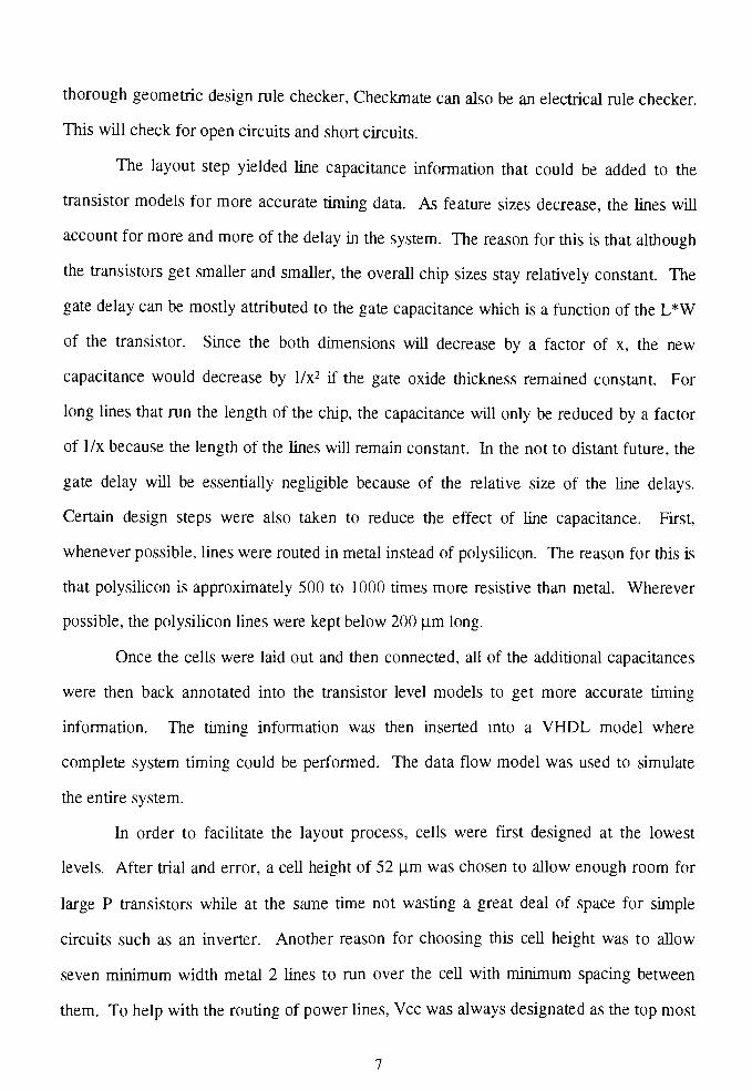
Another convention used in the layout of the microprocessor was serpentining for
extremely large transistors. Figure 1.3 shows an example of a serpentined transistor.
Because there is no standard on how to measure the width of a serpentined transistor, the
convention used in this paper will be to measure the length of the midpoint line. In Figure
1.3, the midpoint line is shown as a dashed line. This dashed line is inside of the
polysilicon mask layer. The large rectangle represents the active mask layer. All other
layers are omitted to make the drawing clearer.
The measurements given all refer to the length, in microns, of the polysilicon over
the active area; in other words, the overhang is not counted. The length of the line can be
measured by starting at point A in the figure. The length is equal to 12 pm down plus 1 1
u.m over plus 8 |im up plus 8 |im over plus 14 pm down for a total of 53 pm.
A
Figure 1 .2 Calculation of the width of a serpentined transistor

The final size of the entire layout before pads was approximately 15 mm by 8 mm.
Because of the enormous size of the final circuit, it will not be fabricated using a 2.0 um
process. In order to reasonably fabricate this design, at least a 0.8 pm process would be
needed to fit the entire chip in a reasonably sized package.
2 Handshaking in Asynchronous Design
Asynchronous design differs from synchronous design since there is no global
clock to control the circuit operation. With synchronous design, all events are triggered
by a clock and all of the events have a defined timing of operations. More than one event
can happen at the same time without worrying about synchronization. With asynchronous
design, there is no global clock to synchronize events. In this design, a controller is placed
between logical blocks to coordinate them. This controller uses start and done signals to
control the flow through the machine.
There are several reasons why the processor was chosen to run asynchronously.
The future of high speed VLSI circuit operation depends on the reduction of long lines. In
synchronous designs, the clock is the heartbeat of the system and its signal must be
globally distributed throughout the entire chip. At very small feature sizes, these lines
become extremely resistive. When driving large capacitive loads using these lines, huge
delays are created which slow down the operation of the processor. When dealing with
clock lines that propagate throughout the chip, clock skew can occur. This condition
occurs when the clock signal takes different amounts of time to get to the various circuits.
When the capacitances get too large, the clock skew can become intolerable. An
asynchronous design philosophy can alleviate the need for long, globally distributed clock
lines throughout the chip.
Another reason to use an asynchronous design philosophy is the amount of idle
time necessary at each pipeline stage. In order for a synchronous design to work
correctly, the processor's clock must be slowed to allow the slowest stage to finish. With
operations that take roughly the same time, this is acceptable. In a processor however,
each pipeline stage may waste an exorbitant amount of time waiting for the next clock
pulse. Statistics say that for a typical ALU instruction, only 50% of a cycle is used to do
work leaving the other 50% as idle time. With an asynchronous design, instead of waiting
10
for the worst case clock pulse to arrive, the system moves on to the next instruction when
each pipeline stage is complete. Although this adds a small amount of overhead to handle
the handshaking, most of the instructions will run faster. Only in the worst or near worst
case situation, should the asynchronous design be slower.
There is a price to pay, however, for the asynchronous methodology. The first
disadvantage is the amount of extra circuitry involved in creating completion signals for
each block as well as the handshaking circuitry. With the present state of VLSI
technology, however, the area on a chip is becoming less and less a factor. Today, most
of the area on a chip is used to make connections between the transistors and to run bus
lines to connect system modules. Another disadvantage of the asynchronous design is the
difficulty in testing the processor to ascertain that deadlock can never occur. A very
useful technique to model asynchronous events is a Petri Net. This structure can be tested
to ensure that deadlock in the processor can never exist.
2.1 Creation of a Completion Signal
The creation of a reliable completion signal was the most important contribution to
performance in asynchronous design. The completion signal must not occur before a logic
block has finished evaluating or the output would be incorrectly latched. It also must not
occur too long after a block is finished or the performance would suffer. In order to
effectively generate a reliable completion signal, Differential Cascode Voltage Switched
Logic (DCVSL) was used. The completion signal controlled each logic block using a start
and a completion signal. To work properly, the block received a start signal, calculated its
result, and set the completion signal high. Figure 2.1 shows the schematic of a DCVSL
block.
11

Figure 2. 1 : Basic DCVSL logic module with a reliable completion signal circuit
This circuit consists of two phases. The first phase is the precharge phase. During
this phase, start goes low and charges Nodes A and B high. This forces out high and done
low. When start goes high, the second phase, called the evaluation phase, begins. During
this phase, either Node A or Node B will be pulled low because the two branches are
duals of each other. This will cause done to go high when the output is valid, assuming
that both branches evaluate at the same time. This condition will be maintained until start
goes low again, producing a complete cycle. The two stage process can produce a reliable
completion signal to be used to determine when the output is valid for the next stage.
12
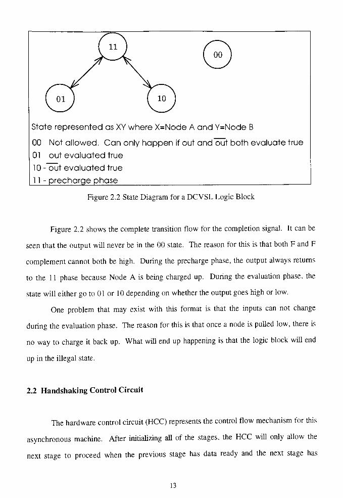
( 01 J ( 10 )
State represented as XY where X=Node A and Y=Node B
00 Not allowed. Can only happen if out and "out both evaluate true
01 out evaluated true
lO- -
out evaluated true
ll -
precharge phase
Figure 2.2 State Diagram for a DCVSL Logic Block
Figure 2.2 shows the complete transition flow for the completion signal. It can be
seen that the output will never be in the 00 state. The reason for this is that both F and F
complement cannot both be high. During the precharge phase, the output always returns
to the 1 1 phase because Node A is being charged up. During the evaluation phase, the
state will either go to 01 or 10 depending on whether the output goes high or low.
One problem that may exist with this format is that the inputs can not change
during the evaluation phase. The reason for this is that once a node is pulled low, there is
no way to charge it back up. What will end up happening is that the logic block will end
up in the illegal state.
2.2 Handshaking Control Circuit
The hardware control circuit (HCC) represents the control flow mechanism for this
asynchronous machine. After initializing all of the stages, the HCC will only allow the
next stage to proceed when the previous stage has data ready and the next stage has
13
latched the data from the HCC's corresponding logic block. The HCC controls the flow
through the use of the done signal mentioned in the previous section. The schematic
diagram for the HCC is shown in Figure 2.3. Table 2.1 gives a description of all of the
signals in the HCC.
Signal Name Description
Init Used to initialize the HCC
Ain Acknowledgment signal from next stage that it has latched thisstages'
data
Ok(n-l) Used to signal that the previous stage has completed its operation
Ready Signal from the present logic block to indicate its operation has completed
Aout Acknowledgment to previous stage thatits'
data has been latched
Rout Start signal for the next logic block
Ok(n) Signals next stage that this stage has completed
Table 2. 1 Definition of the Signals in the HCC Circuit
The HCC starts when Ok(n-l) goes low. This signal means that the previous stage
has valid data. When both Rout(n) and Ready(n) are both low, the HCC raises Aout(n) to
send an acknowledgment back to the previous stage. When Aout(n) goes high and Ain(n)
is low, Rout(n) goes high. Rout(n) is the start signal to the current logic block as well as a
signal to latch the previousstages'
data. At this point, the HCC waits for the completion
signal, Ready(n), of the current logic block to go high. When it does it lowers Ok(n)
indicating to the next HCC that this logic block has valid data. The HCC then expects
Ain(n) to go high, an acknowledgment from the next HCC that the data has been latched.
When the happens, Rout(n) goes low to start the precharge phase for the logic block. This
triggers Ready(n) low and the process repeats itself.
14

Figure 2.3 Schematic Diagram for the Handshaking Controller Circuit
15

The implementation of the HCC used minimum sized transistors to minimize the
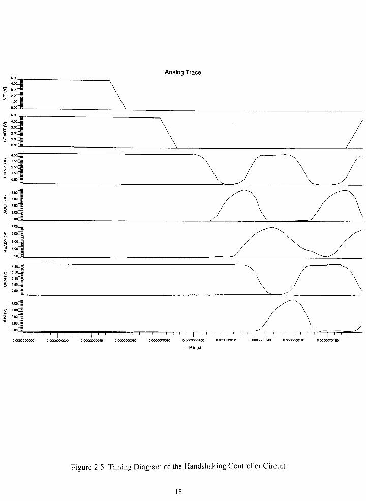
input gate capacitance. In order to test the amount of overhead the HCC put on the
system, three different HCCs were connected as shown in Figure 2.4. As shown in this
figure, the timing data was taken from the center controller so that the data will be nearly
identical to the actual processor. The timing diagram for the test HCC circuit is shown in
Figure 2.5. The layout for the HCC block is shown in Figure 2.6.
The system was initialized by forcing Init high. This initialization set the HCC to a
starting state and could be used to stop the HCC. Once Init went low, the first HCC
waited for the Ok(n-l) signal to go low. This was accomplished by lowering the start
signal. As long as the start signal remained low, the HCC would operate. In order to only
measure the delay caused by the HCC, the Rout(n) was directly connected to the
Ready(n). This configuration was equivalent to a zero delay logic element. From Figure
2.4, the total delay time was calculated to be 5.7 ns.
16

A- n.-
*p osa
(no(j
CU
0
CO
<=> <
(post
I nog
o -a
*posjj
I n"B
A A
0 0
<X CD
0 0
o
Figure 2.4 Circuit used to calculate the timing information for the HCC
17
Analog Trace
2.00_|
o.oo_g.
5._i
1 i i i |i i i i | i i i i i i i i i i i i i i
|i i i i l i i i i
[0 0OOOOOOOO0 0 0000000020 D 0000000040 0 0000000060 0.OO0O000080 0.0000000100 0 0000000120 0.0000000140
TIME (s)
i i i r
00000000160 0 0000000180
Figure 2.5 Timing Diagram of the Handshaking Controller Circuit

Figure 2.6 Layout of the Handshaking Controller Circuit
19
3 Pipeline Structure
The MIPS R3000 processor uses a five stage pipeline which will also be used for
the asynchronous design. The five major stages are: Instruction Fetch (IF), Instruction
Decode (ID), Arithmetic Logic Unit (ALU), Access to Memory (MEM), and Register
Writeback (WB). These are shown in Figure 3.1. The five stages allow significant
parallelism to be incorporated into sequential code. This parallelism is attained by dividing
each instruction into five sections. By doing this, each stage of the pipeline can operate on
a different instruction. If each stage is constantly busy, a speed up of five is attained. To
illustrate this point. Figure 3.2 shows a certain time slice of the pipeline stage. At time t5,
the IF stage is fetching Instruction 15. Also, the ID stage is decoding 14. The ALU stage
is working on 13. The MEM stage is operating on 12 and the Writeback stage is at 77.
This shows that the pipeline can be working on 5 different instructions at once. Figure 3.3
shows that for a 10 instruction program executed on a pipelined machine and a non-
pipelined machine. For this example assume that an instruction takes 10 time units to
complete. In the pipelined case, this 1 0 time unit instruction is divided into 5 stages of 2
time units each. As can be seen, the pipeline machine will take only 28 time units while
the non-pipelined machine will take 100. As the number of instructions increases, the limit
of the speed up will reach five.
20
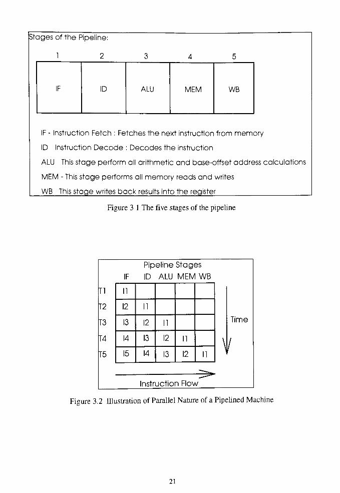
Stages of the Pipeline:
12 3 4 5
IF ID ALU MEM WB
IF - Instruction Fetch : Fetches the next instruction trom memory
ID Instruction Decode : Decodes the instruction
ALU This stage perform all arithmetic and base-offset address calculations
MEM - This stage performs all memory reads and writes
WB This stage writes back results into the register
Figure 3. 1 The five stages of the pipeline
IF
Pipeline Stages
ID ALU MEM WB
Tl
T2
T3
T4
T5
11
12 11
13 12 11
14 13 12 11
15 14 13 12 11
Time
V
Instruction Flow
Fiaure 3.2 Illustration of Parallel Nature of a Pipelined Machine
21
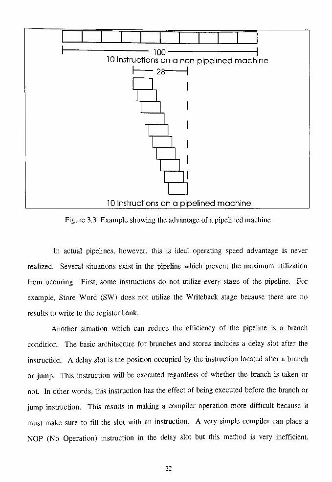
100 110 Instructions on a non-pipelined machine
I 28
10 Instructions on a pipelined machine
Figure 3.3 Example showing the advantage of a pipelined machine
In actual pipelines, however, this is ideal operating speed advantage is never
realized. Several situations exist in the pipeline which prevent the maximum utilization
from occuring. First, some instructions do not utilize every stage of the pipeline. For
example, Store Word (SW) does not utilize the Writeback stage because there are no
results to write to the register bank.
Another situation which can reduce the efficiency of the pipeline is a branch
condition. The basic architecture for branches and stores includes a delay slot after the
instruction. A delay slot is the position occupied by the instruction located after a branch
or jump. This instruction will be executed regardless of whether the branch is taken or
not. In other words, this instruction has the effect of being executed before the branch or
jump instruction. This results in making a compiler operation more difficult because it
must make sure to fill the slot with an instruction. A very simple compiler can place a
NOP (No Operation) instruction in the delay slot but this method is very inefficient.
22

Optimizing compilers will reorder the instructions so that the delay slot can be filled with a
meaningful instruction to take advantage of this architectural feature.
The delay slot technique will reduce the amount of pipeline stall time. A branch
predictor will be correct 50% of the time. Using a delay slot after the instruction, a
meaningful instruction can be inserted as much as 75% of the time. If no meaningful
instruction can be placed in the delay slot, a wasted instruction must be placed there. This
condition is called a control hazard.
Another condition which reduces the efficiency of the pipeline is called a data
hazard. This condition occurs when a data dependency exists in the executing code.
When this occurs, the dependent instruction must wait the for the results of the
independent instruction to be written back to the register bank.
The final condition that affects the pipeline occurs when certain stages finish before
other stages. When this occurs, the completed stage must wait idly for the other stages to
complete. This also adds to the inefficiency of the pipeline.
3.1 Instruction Fetch Stage
The Instruction Fetch Stage (LF) is responsible for fetching the next instruction.
The schematic for the IF block is shown in Figure 3.4. It generates a memory request to
the memory controller to receive the next instruction. It then gets the physical memory
address from the address adder in the ID. After fetching the instruction, the instruction is
passed onto the ID stage. In addition to the fetching, the LF stage performs one other
important feature; it handles branching to an interrupt vector when an exception occurs.
The interrupt controller physically resides next to the Instruction Fetch and will signal
when the IF needs to load instructions from the interrupt vector instead of the current
program counter. Because of this feature, the interrupt mechanism is made simpler and
less disruptive to the pipeline.
23

The IF stage is started from the start signal, generated from the HCC. When it
receives the start signal, it waits for addr_valid to go low or an interrupt to occur. When
addr_valid goes low, the ID has calculated the next address to fetch from memory and the
IF will issue a memory request to the bus controller to get the next instruction. At this
point, the IF must latch the address coming from ID. The IF stage must wait until the bus
controller sets ia high signaling that the IF can now put the address on the bus. This
acknowledgment signal is needed to allow the address bus to be set before the memory
read. When the address is loaded onto the bus, the il line is set high to tell the bus
controller to initiate the request. The LF then waits until the ia line goes low signaling that
the data bus now contains the valid instruction. The LF stage then latches the data and
resets the ir and il line signaling the bus controller that the bus is now free and can be
used. The waveforms showing the operation of the IF stage is shown in Figure 3.5.
The address to be put onto the bus can come from two places: the address adder,
(new_pc) and the Exception Handler, (iv). During normal operation, the IF block will
fetch the next instruction located at the address new_pc points too. When an exception
occurs, the interrupt vector will be put onto the memory bus simulating a jump to the
interrupt vector. This project will not support exceptions because the state of the machine
will not be saved when an exception occurs.
Before the IF stage requests memory, however, one of two conditions has to be
met. The first condition is that an exception occurs. In this case, the LF will read the next
word at the interrupt vector specified by the exception handler. If there is no exception
present, the IF stage must wait for the addr_valid line to go low. The addr_valid line is
set high to allow the address adder time to calculate the next address.
24

CD
(0
GO
O
71
o
0 A
i
C
O
0
o CD
,_
oo OO*-? ^^
>-v -~J
3 O Do _o oX i .
a> L. OO ,.
i TD W
-i_ o o c-
<D Q.
0 0
i
'I at
6 6 6 6 6 6CT
CO
L_ CO
>
C_
X)
T3
C
6 6
A
o GO cr
-rt
._
OO oo oo- - s_.
c > cQ. " -
3 CC
w .
C c
Figure 3.4 Schematic Diagram of the Instruction Fetch Stage
25

u u
j
6
ft
I
1'ISIo i 5
,
i |'
;i* . Q " W
I, O C
111 o!ir< i- S
^
' r*<
! CD g
oo
oo
: '8 9
S ; -
,, |
g ;g 8 ;||i : 8 |
ift ^; iS; 'J:
S 8. S=, 3 j .o
"5 5 "8 5
Figure 3.5 Waveforms showing theoperation of the IF Stage
26

A tri-state buffer is placed to drive the address bus. The LF stage must be isolated
from the address bus when the MEM stage uses the bus. The schematic for the tri-state
buffer is shown in Appendix C in the miscellaneous circuit section.
3.2 Instruction Decode Stage
The Instruction Decode (ID) stage is the second stage in the pipeline. The
Instruction Decode has several functions. The first function is to decode the instruction
into several categories so that the processor can execute correctly. The second function is
to provide an address adder to calculate the destination address for all branches and jump
and to increment to Program Counter (PC) on all non branch or jump instructions. The
final task the ID must implement is a way of stalling the pipeline when a data dependency
occurs. These three tasks will now be explained in more detail. The overall schematic
Diagram of the ID stage is shown in Figure 3.6.
3.2.1 Decoding
The first function of the ID stage is the decode the instruction into seventeen
different categories. These categories are given below. Not only does the LF stage need
to know some of these things, but the ALU stage must also be provided with this
information to relieve it from some decoding. The 17 categories and signals are:
27

CD
O)
CD
XO
JD
O
o
CD
o
(/)
Figure 3.6 Schematic Diagram of the Instruction Decoder Stage
28

1) Illegal Instruction (ILL) This signal goes high when an illegal
instruction is identified by the instruction set.
2) Testing 1st source register dirty bit (TS1) -This signal is high when the
first source register must be tested for a data dependency problem.
3) Testing 2nd source register dirty bit (TS2) - This signal is high when the
second source register must be tested for a data dependency
problem.
4) Testing destination register dirty bit (TTAR) This signal is high when
the destination register must be tested for a data dependency
problem.
5) Testing HI register dirty bit (THI) This signal is high when the HI
register must be tested for a data dependency problem.
6) Testing LO register dirty bit (TLO) This signal is high when the LO
register must be tested for a data dependency problem.
7) Branch (Conditional) (BRA) This signal is high when the instruction is
a branch.
8) Jump (Unconditional) Instruction (JUMP) This signal is high when the
instruction is a jump.
9) R Instruction (R) Constitutes either a Jump Register (JR) or a Jump
and Link Register (JALR) instruction.
10) L Instruction (L) Constitutes either a Jump and Link (JAL) or Jump
and Link Register (JALR) instruction.
11) Immediate or Base-offset Calculation Instruction (LBO) This signal
will go high on either an immediate instruction or an instruction that
requires the ALU to perform a base-offset calculation.
12) Software Exception (SYSCALL or BREAK) (EXC) This signal will
go high when the instruction is either SYSCALL or BREAK.
13) MDU select (MDU_SEL) This signal goes high when the MDU is
activated.
14) ALU select (ALU_SEL) This signal goes high when the ALU Is
activated.
15-16) Signals to determine the destination register (TRSO) and (TRS1).
The four possibilities are shown in Table 3. 1.
17) (ADD8_SEL) Signal used to activate the ADD8 Unit in the ALU
Stage
29
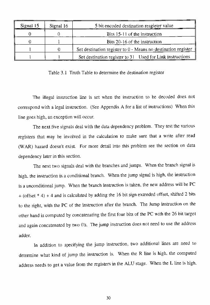
Signal 15 Signal 16 5 bit encoded destination resgieter value
0 0 Bits 15-11 of the instruction
0 1 Bits 20-16 of the instruction
1 0 Set destination register to 0 - Means no destination register
1 1 Set destination register to 3 1 Used for Link instructions
Table 3. 1 Truth Table to determine the destination register
The illegal instruction line is set when the instruction to be decoded does not
correspond with a legal instruction. (See Appendix A for a list of instructions) When this
line goes high, an exception will occur.
The next five signals deal with the data dependency problem. They test the various
registers that may be involved in the calculation to make sure that a write after read
(WAR) hazard doesn't exist. For more detail into this problem see the section on data
dependency later in this section.
The next two signals deal with the branches and jumps. When the branch signal is
high, the instruction is a conditional branch. When the jump signal is high, the instruction
is a unconditional jump. When the branch instruction is taken, the new address will be PC
+ (offset * 4) + 4 and is calculated by adding the 16 bit sign extended offset, shifted 2 bits
to the right, with the PC of the instruction after the branch. The Jump instruction on the
other hand is computed by concatenating the first four bits of thePC with the 26 bit target
and again concatenated by two 0's. The jump instruction does not need to use the address
adder.
In addition to specifying the jump instruction, two additional lines are need to
determine what kind of jump the instruction is. When the R line is high, the computed
address needs to get a value from the registers in the ALU stage. When the L line is high,
30

the instruction is some form of jump and link. When this occurs, the ID stage must give
the ALU stage the PC so that it can compute the link address of PC + 8.
The next line, the Immediate or Base-Offset signal, is needed by the ALU stage for
the selecting one of the branches to the ALU. This condition is high on either an
immediate or base offset instruction. Base-offset instructions include all load and store
instructions but not branch instructions since the ALU does not do the calculations for
these. For both immediate and base-offset instructions, the 16 least significant bits are
placed on one of the ALU inputs.
The twelfth signal to be computed is a software exception. These consist of either
a SYSCALL or BREAK instruction. Both of these instructions will cause an exception to
occur.
The thirteenth and fourteenth signals define which unit in the ALU stage will be
active. The ALU select will enable the ALU and disable the MDU while the MDU select
does the opposite. When both of these lines are low, neither unit is operational.
The fifteenth and sixteenth signals specify where to get the destination register
address from. There are four different cases shown in Table 3. 1 . The first case occurs in
all SPECIAL insU'uctions. In this case, the destination register address is located in bits
15-11 of the instruction. The second case exists for load, stores and immediate
instructions. These instructions contain a 16 bit constant value in the instruction so the
destination register is moved to bits 20-16 for these cases. The final case for a valid
destination register address is the instruction Jump and Link (JAL). This instruction will
automatically use register 31 is the destination for the link address. For any other
instruction, there is no destination register and a value of 0 will be substituted since the
register 0 is hard wired to the value 0. The dirty bit will also be hard wired clean to allow
an instruction with no destination to operate properly. These four cases are implemented
using a 4-1 multiplexer.
31
Signal 17 is used by the ALU stage to start to ADD8 Unit. This unit is only used
on Branch Conditional Instructions which need a link address calculated. The reason this
unit is needed is that the Address Adder must calculate the Branch Destination and the
ALU must calculate the condition code.
Because of the enormous decoding that must be done for this stage, a logic
mirdmization tool was used to reduce the number of gates in the decoder. The tool used
was espresso. Although espresso does not guarantee the absolute minimum logic, it is a
very good logic minimization tool. A commented version of the input file and the output
file are shown in Appendix B.
The decoder was done using standard gates instead of a PLA because of the size.
This would consist of 16 inputs, 17 outputs and 35 product terms. Another reason the
PLA structure is not used is that the product terms would have up to 12 inputs. The
actual implementation involved breaking up both the AND and the OR section into two
stages each so that a 4 input gate was the maximum size. If this was implemented using a
PLA structure, the speed penalty due to the length of polysilicon lines needed would be
too large. The schematic diagram of the decoder is shown in Figure 3.7.
3.2.2 Address Adder/Incrementer
The second task the LF stage must perform is the address calculations for all
branches and jumps. The ID contains a separate address adder/incrementer, referred to as
simply address adder, which frees the ALU from this task. When a conditional branch or
jump occurs, the address adder will calculate the destination address. If the instruction is
not a branch or jump, the address adder will increment the PC.
32

'nst3>ri>-
Instruct ion Decode Block
^^MD_SEL
Figure 3.7 Schematic Diagram for the Decoder in the ID Stage
33
The Address Adder is implemented using a 30-bit Conditional-Sum Adder. The
Conditional-Sum Adder is described in more detail in Section 3.3. The reason only 30 bits
was chosen was because the least significant two bits must be 0 so that the instruction is
aligned on a word boundary. When this is not the case, an exception will occur. Another
reason for only 30 bits is due to the delay associated with the adder. A conditional-sum
adder has a delay equal to the ceiling function of (log2 n) 1 . Therefore to make the adder
32 bits would introduce unnecessary additional delay.
The adder uses DCVSL logic to generate a completion signal. The address adder's
start signal goes high when the start signal for the ID stage goes high and one of two
conditions exist. If the last instruction was a branch, the start signal must wait for ccd.
ccd goes high when the ALU stage is done calculating the condition code. The second
condition to wait for is when the instruction is neither a branch nor a jump. The reason
the start signal goes high during a jump instruction is that the decoder needs time to
decode the instruction.
There are four possible calculations that the address adder must perform. The first
calculation is to perform addition on all branches that are taken. This is done by adding
the Program Counter of the delay slot instruction with the sign extended 16-bit offset.
This offset value is located in bits 15-0 in the instruction. The second calculation is
performed on jump instructions that must get the destination from a register. The
constitutes two instructions: Jump Register (JR) and Jump and Link Register (JALR).
These two instructions cause the value in register to be loaded into the program counter.
The third calculation is done on jumps that don't use the register. These case involves two
instructions: Jump (J) and Jump and Link (JAL). For this case, the most significant 4 bits
of the current program are concatenated with a 26-bit target address given in bits 25-0 of
the instruction. This 30-bit value is then concatenated with two zeros to get the new
address. The final calculation covers the remaining instructions. During this calculation,
the program counter is incremented by one word or 0x00000004.
34
In order to implement the adder, a unit called BJBOX (Branch and Jump Box) is
placed above the second input of the address adder to control what gets added. The
schematic for BJBOX is shown in Figure 3.8. The unit consists of a 4-1 multiplexer which
will select among the various calculation described above. For jump instructions, the
address adder will be bypassed since there is no addition involved. This can be shown in
Figure 3.7 which shows the entire schematic of the Instruction Decode stage. This
bypass is implemented through the multiplexer whose select line is the J latch which
signifies the last instruction was a jump.
3.2.3 Data Dependencies
A final task for the ID is to detect data dependencies. The ID stage does this by
querying the dirty bits that may be used in the instruction. The dirty bit actually consists
of two additional bits in each register, designated as db_id and db_wb to indicate which
stage sets them. The reason that two bits are used is that the ID stage must set the dirty
bit to indicate that the value in the register is no longer valid and the Writeback stage must
reset it to indicate that the register has been updated and its contents are now valid. This
leads to a mutual exclusion problem. This problem does not exist if two bits are used.
This new scheme allows the IF stage to toggle one side and the Writeback stage
toggle the other side. Initially both bits are set to 0. When the ID stage decodes an
instruction that requires a value to be written to a register, it will place the decoded
register value on treg_out. This value is only valid when not equal to zero because by
convention, register 0 is always clean. When the ALU start signal goes high, the db_id
value will be toggled. By toggling the bits, the bits can be exclusive OR'd together to
generate the dirty bit value. Once the db_id bit is set, the dirty bit will then show the
register as dirty. The ID stage must stall all instructions that use this register until the
Writeback stage writes the value into the register and sets db_wb.
35

CJ
O
en
oo
ex.
Q
O
0
^
TD
o
06
X)
CD
:>
CD
CD
o
CD
CD
O
CD
CD6o
LD
OJ
C
b
en
oo
O
a w
L^
o
00'
o
Q.
1
5 S 5? w
^ "6 6
Figure 3.8 Schematic Diagram of BJBOX
36
Since db_id and db_wb will never be signaled twice in a row, the order these two
bits will follow, assuming db_id come before db_wb will be 00 10 11 01 00. This
cycle will constantly repeat. In order for no deadlock to occur, all of the dirty bits must be
initialized to either a 00 state or a 1 1 state. For this machine, they will be initialized to 00.
For more information on the implementation details of the dirty bits, see Design and
Implementation of an Asynchronous Version of the MIPS R3000 Microprocessor by
Kevin Johnson.
In order for ID to halt all data dependent instructions, it must know which
registers to test. This job is handled by the Decoder. The decoder generates 5 bits to
determine which dirty bits to test. They are Test Source Register #1 (TS1), Test Source
Register #2 (TS2), Test Target Register (TTAR), Test Hi Register (THI) and Test Lo
Register (TLO). When these signals are high, the register must be tested. For example
the instruction Add Immediate (ADDI) has no Source #2 register so this value does not
need to be tested.
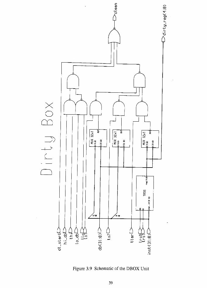
The unit that implements the dirty bit testing is called Dirty Box (DBOX) and is
shown in Figure 3.9. The DBOX unit will input the instruction, the five test signals, as
well as TRS0 and TRS1. TRS0 and TRS1 will be select lines to a 4 by 1 multiplexer that
will generate the target register whose value will be used to set the db_id. DBOX consists
of five different tests. If the test line is low, it will automatically cause a 1 to be put on the
NAND gates. When it is high, it will invert the dirty bit. Therefore if the dirty bit is high,
it will put a zero and clean will than stay low. The done signal will only go high on the
rising edge of clean. Thus, the done signal will wait until the Writeback stage toggles the
db_wb line which will cause the dirty bit to go low again raising the clean bit.
Ln addition to the NAND gates, a 32 by 1 multiplexer will select the correct dirty
bit for each general purpose register. These 32 by 1 registers are implemented using
cascaded 2 by 1 multiplexers. The schematic is shown in Appendix C with other general
cells. The other large cell in this unit is the Target Register Dirty Select (TRDS) Unit.
37

This Unit will generate the destination register of the instruction or 0 if no destination
register exists. The schematic for this circuit is shown in Figure 3.10. This circuit is a 4
by 1 multiplexer that selects between the four cases given in Table 3. 1.
By using this implementation scheme, we have given the architecture more
flexibility. In the synchronous architecture, a delay slot was needed for data dependencies
to guarantee the results of the operation would be written back into the register bank. In
this asynchronous version however, this can not be guaranteed any longer. The advantage
of allowing data dependant instructions to follow each other is that code written for the
asynchronous version can functionally run correctly, unlike the synchronous version. The
disadvantage is that this case will be equivalent to adding a NOP instruction because the
pipeline is still stalled while instruction waits to be written back into the registers.
3.3 Arithmetic Logic Unit Stage
The Arithmetic Logic Unit (ALU) stage consists of three units running in parallel.
They are the Arithmetic Logic Unit, the Multiplier/Divider Unit and the Add8 Unit. The
ALU stage is responsible for all of the arithmetic calculations that must be done by the
processor. It also contains the general register bank and the tag bits associated with the
data dependencies. The ALU section was designed by Kevin Johnson and can be found in
Design and Implementation of an Asynchronous Version of the MIPS R3000
Microprocessor.
38
X
o
m
<)
o
cihhhcn*>
_o
-
_o
cr~
L. -o -C X3 -^
CD |
CO
c
Figure 3.9 Schematic of the DBOX Unit
39

Target Register Dirty Select
vcc
;t_in(31:0)E>
MW/
INS
IN1
IN?
IN3
OUT
INS
IN1
IN3
OUT
INO
IN1
1N2
IN3
OUT
m .-
INO
INI
IN2
IN3
OUT
INO
INI
IN2
IN3
OUT
Oreg(tO)
Figure 3.10 Schematic of the TRDS Unit
40

4e
a>AfWWfl-l/l
(VW?YA
6 6
Figure 3. 1 1 Schematic Diagram of the Multiply/Divide Unit
41

o
CD
o
CO
c_
O)
CD
o
G
Figure 3. 1 2 Block Diagram of the Multiplier/Divider Unit
42
3.3.1 Multiplier/Divider Unit
The Multiplier/Divider Unit (MDU) was added to the processor to unburden the
ALU from time consuming multiplications and divisions. In the 50 MHz synchronous
version, the multiply instructions took 12 clock cycles or 240 ns and divide instructions
took 35 clock cycles or 700 ns. Ln the asynchronous version, the MDU takes a long time
to complete. Both multiplications and division take approximately 1 ps to complete.
Even at this speed, programs with extensive multiply and divide operations would suffer in
performance without the MDU. The disadvantage of the MDU was the extra circuitry
used. This represented a big penalty since the area used was roughly the twice the size of
the ALU. The schematic diagram of the entire MDU is shown in Figure 3.1 1. In order to
clarify the operation, a block diagram is also included in Figure 3.12.
The hardware implementation of the MDU has been modeled after an algorithm
designed by Andrew D. Booth. [3] It can handle signed two's complement numbers for the
multiplier and unsigned numbers for the divider. Both the multiplication and division have
several similarities which allows them to be combined into one unit effectively. The first
similarity is that both can be effectively done using three operations: shifting, addition,
and subtraction. Another similarity is that both can be calculated essentially using three
32-bit registers for temporary storage. Finally, both can be implemented using a finite
state machine.
The theory behind Booth's Algorithm is to reduce the number of additions and
subtractions necessary for each bit in the multiplier. Elementary multiplication is
performed using one digit, or bit, at a time. Using this algorithm, a group of bits, called a
block, can now be examined at once, reducing the average number of additions and
subtractions. The size of the block, therefore, makes a big difference in the performance
of the algorithm. A large block size obtains much better performance than a small block
size. The disadvantage of the large block size is that it can only be recognized by making
43

the adder/subtractor unit much more sophisticated. With higher block sizes, the
adder/subtractor not only needs to add the multiplier but also multiples of the multiplier.
Another unit would then have to be added to generate these multiples which makes the
algorithm much more complex. In order to make this clearer, the design for one and two
bit blocks will be described. In addition, a modified version of the two-bit block size will
be described.
The one-bit block is similar to elementary multiplication except in binary form. Ln
this form, multiplication is performed by taking the least significant digit in the multiplier
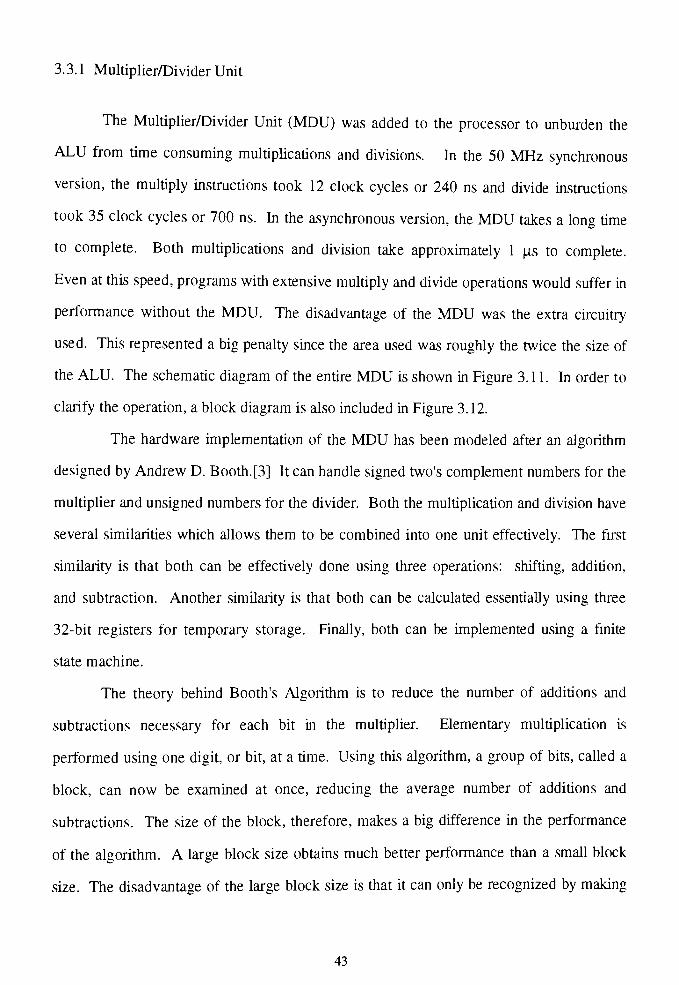
and operating on the multiplicand. A partial sum is formed for every digit, each sum being
shifted over one place more than the previous partial sum. The computer deals with
binary digits instead of base 10 numbers. A binary number format makes the operation
much simpler because there are only two possible digits. If the digit is a one, the
multiplicand is added to the partial result and the partial sum is then shifted. If the digit is
zero, the partial result is simply shifted. The problem with this method is that there can be
up to n additions for an n by n multiplication with an average of nil additions. The
advantage is that the hardware is extremely simple because only an adder and three
registers, two being shift registers, are needed.
The two bit block is the simple form of Booth's algorithm. By scanning the
multiplier two bits at a time, there are four different results that can occur, instead of two
for the one bit case. Table 3.2 shows the results of the four different cases.
44
Xixl Xi Result
0 0 No action
0 1 SubtractMultiplicand
1 0 Add Multiplicand
1 1 No action
Table 3.2 Truth table for scanning a two bit block
By scanning two bits at a time, the algorithm skips over runs of zeros or ones in
the multiplier. A problem is encountered with this algorithm when the ones and zeros are
isolated, for example 1010 10101. In this case, the efficiency of the algorithm remains
the same as the one bit block. Therefore, because of the extra hardware required, this
implementation would be a waste of hardware. In order to get around this problem, a
modified form of Booth's algorithm was implemented.
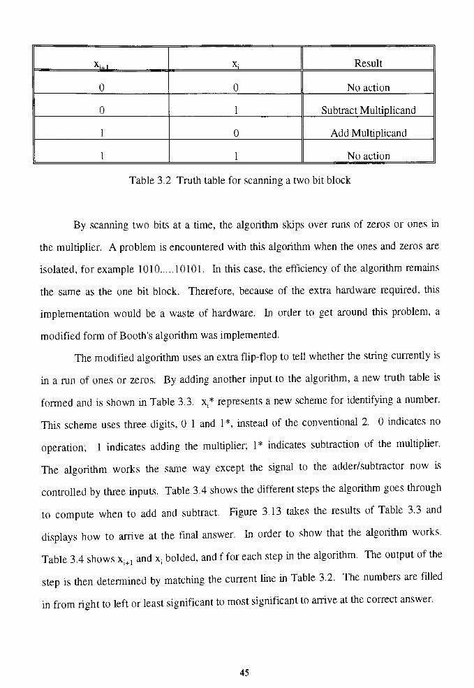
The modified algorithm uses an extra flip-flop to tell whether the string currently is
in a run of ones or zeros. By adding another input to the algorithm, a new truth table is
formed and is shown in Table 3.3.x,*
represents a new scheme for identifying a number.
This scheme uses three digits, 0 1 and 1*, instead of the conventional 2. 0 indicates no
operation; 1 indicates adding the multiplier;1* indicates subtraction of the multiplier.
The algorithm works the same way except the signal to the adder/subtractor now is
controlled by three inputs. Table 3.4 shows the different steps the algorithm goes through
to compute when to add and subtract. Figure 3.13 takes the results of Table 3.3 and
displays how to arrive at the final answer. In order to show that the algorithm works.
Table 3.4 shows xi+1 and xs bolded, andf for each step in the algorithm. The output of the
step is then determined by matching the current line in Table 3.2. The numbers are filled
in from right to left or least significant to mostsignificant to arrive at the correct answer.
45
xi+l X; f*
f Comments
0 0 0 0 0 middle of a run of Os
0 1 0 1 0 x, is an isolated 1
1 0 0 0 0 ends a run of Is
1 1 01*
1 x^ begins a run of Is
0 0 1 1 0 x^ begins a run of Os
0 1 1 0 1 ends a run of Os
1 0 11*
1 X; is an isolated 0
1 1 1 0 1 middle of a run of Is i
Table 3.3 Truth table for the modified Booth's algorithm
Two bits highlighted f New digit
Result to operate on the
parital sum
000110110 0 0 No action
000110110 0 1* Subtract Multiplicand
000110110 0 No action
0001101101* Subtract Multiplicand
000110110 0 No action
000110110 0 No action
000110110 1 Add Multiplicand
000110110 0 0 No action
Table 3.4 Steps for an example using the modified Booth's algorithm
46
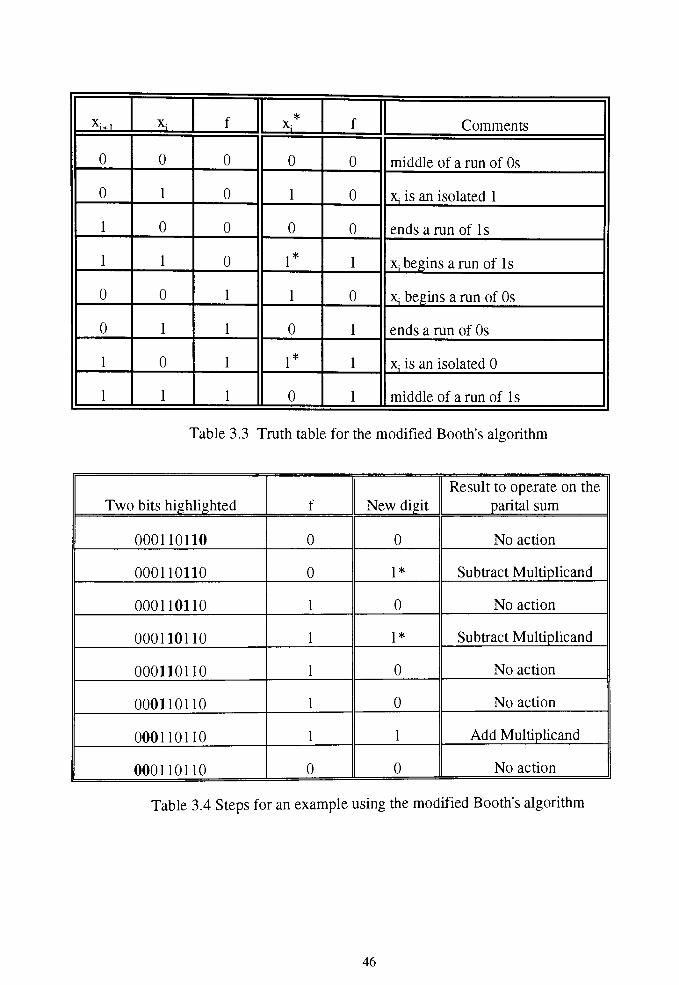
Example: Multiply 54 by 9 assuming 8 bit registers
Multiplicand is 9 or 0000 1001
Multiplier is 54 or 001 1 01 10
The multiplier is converted using Table 3.3 and the resulting string is, following upthe New digit column in Table 3.4= 01001*01*0
All 1 represent an add, all 1 * represent a subtract
therefore Z= 9x26- 9x23- 9x2J = 576 - 72 18 = 486, the correct answer
Figure 3.13 Example showing how Booth's Algorithm works
The perfonnance of a multiplication algorithm is inversely proportional to the
average number of additions and subtractions. For the one bit block case, it is obvious
that there will be nil additions because on average half of the digits will be ones. Ln the
regular Booth's algorithm, there will be again an average of nil addition and subtractions.
The modified Booth's algorithm will produce only n/3 additions and subtractions, making
it more efficient.
The multiplier is the first of the two operations the MDU performs. The pseudo
code for the multiplication algorithm is shown in Figure 3.14.
There are several different states that the algorithm must go through. Because of
this, a finite state machine was used to implement the multiplication. The state diagram
and corresponding state definitions areshown in Figure 3.15.
Like the multiplier, the divider is also implemented using afinite state machine. By
manipulating the algorithm slightly, the divider can be implemented using the same finite
state machine as the multiplier. Figure 3.15 also shows the division operations done at
each stage. By combining the operations, an overlapped MDU finite state machine Is
obtained. The state machine is then used to design the first large unit, the
Multiplier/Divider Controller (MDC) . The schematic diagram of the MDC is shown in
Figure 3.16.
47
The MDC controls the flow of the MDU using a local high speed clock with a
period of 1 1 ns to allow for the ASU to finish. It uses edge triggered D Flip-flops to
switch between the states. Ln addition to the current state, there are two other variables
that are used in switching states. They are the counter output and the zero_test output.
The zero_test output is used to speed up operations where one of the operands is zero.
Since the compiler is responsible for handling divide by zero cases in division, any time
any operand is zero, the resulting answer will be zero. The counter output will count up
to 33 and then set the output high. This tells the controller to exit the loop of the
algorithm and output the answer.
Since the Adder/Subtractor Unit is slowest element in the MDU, it is the
determining factor in how fast the local clock can run. The maximum delay in the ASU
was calculated at 7.8 ns so the local clock will run at 8 ns to allow for a small safety
factor. In addition to these major blocks, the other components in the MDU are an
adder/subtractor unit and a complementer.
The next logical piece in the MDU are the three registers: the Q, A, and M
registers. The Q register holds the lower 32 bits of the multiplication and the product for
the division. This register must be a shift register because both left shifting and right
shifting need to be done by this register. In addition to shifting, this register must also be
able to set the least significant bit (LSB) for the division algorithm to work. The A
register is the accumulator register. The final register, the M register, holds the
multiplicand or divisor depending on the operation. For all of the registers, this number is
loaded at the beginning and never changes throughout the duration of the evaluation. For
this reason, the M register does not need to be a shift register.
48
Pseudocode for the multiply algorithm
A = 0, COUNT = 0, F = 0, LOAD M and QSetQ32 = Q(31)
IF M=0 OR Q = 0 GOTO OUTPUT
LOOP: IF F = 0
IFQ(1:0) = 01 A = A + M
ELSEIFQ(1:0) = 11 A = A M, F = 1
ELSE GOTO TEST
IFF= 1
IFQ(1:0) = 00 A = A +M,F = 0
ELSEIFQ(1:0) = 10 A = A M
TEST: IF COUNT = 3 1 GOTO OUTPUT
RIGHT SHIFT A.Q32.QCOUNT = COUNT + 1, GOTO LOOP
OUTPUT: RIGHT SHIFT Q32.QEND
Pseudocode for the divide algorithm
COUNT = 0, S = 0. LOAD Q and M, A = 0, S.A = S.A M
IFQ<0 COMPLEMENT INPUT
IF M < 0 COMPLEMENT INPUT
SIGN = (Q < 0) XOR (M < 0)
TEST: IFS = 0
Q(n-l)=l
IF COUNT = n- 1 GOTO CORRECTION
ELSE
COUNT = COUNT + 1
LEFT SHIFT S.A.Q
S.A = S.A M GOTO TEST
ELSE
Q(n-1) = 0
IF COUNT = n-1 GOTO CORRECTION
ELSE
COUNT = COUNT + 1
LEFT SHIFT S.A.Q
S.A = S.A + M GOTO TEST
CORRECTION: LFS=1
S.A = S.A + M
IF SIGN = 1 COMPLEMENT OUTPUT
Figure 3.14 Pseudocode for the Multiplication and Division Algorithms
49

State Diagram for theMultiplier
Multiply States
0: Initialize Q, A, M and F registers to 0. Initialize Q33 with Q32
1 : Load in the Q and M registers
2: Load in F
3: Perform addition or subtraction if necessary
4: One final right shift of Q
5: Output the results
6: Test the count loop
7: Right Shift
Divide States
0: Initialize Q, A, M, S and LAST_S registers to 0. Calculate SIGN
1: Load in the Q and M registers and Complement if needed
2: Set Q if necessary
3: Perform addition or subtraction
4:lfS= l.AddM
5: Output the results and Complement if needed
6: Test the count loop
7: Left Shift
Figure 3. 1 5 State Diagram for the Multiplier
50

MD_Controller
q<31:0)C
n(31:G)C
clockO-
startC^
div_selC>-
twi
>T
wm
vcc
D i 0-
cl
D S 0
at
YV
-OcQ
-Od
-Oc2
Ficure 3.16 Schematic Diagram of the Multiplier/Divider Controller
51

In addition to the three 32-bit registers, there are five additional one-bit registers.
They are the F, S, LAST_S, Q32 and SIGN registers. The F register determines whether
to add or subtract the M register in the multiplication process. The S register contains the
33rd and most significant bit for the ASU and is only used for unsigned division. An extra
bit is needed because the division algorithm does a subtraction to determine the
comparison. The LAST_S register stores the S bit from the last add or subtract to
determine whether to set the LSB in the division algorithm. The Q32 register is used as a
buffer between the A and Q registers in the multiplier. The SIGN register is used to
determine whether the output of a signed division should be two's complemented or not.
A B c F
A = load enable
B = shift_enable
C = left_shiff
F = operation (S0S1)
00 = No operation
01 = Right Shift
10 = Left Shift
1 1 = Load
SO = B + CD
Sl = B + CLY
0 0 0 00
0 0 1 00
0 1 0 01
0 1 1 10
1 0 0 11
1 0 1 11
1 1 0 11
1 1 0 11
Table 3.5 Truth Table to determine operation in a register
The design of the 32-bit shift register for the MDU was done hierarchically. First a
one bit register was designed to accommodate both set and clear. Secondly, a 4 bit-shift
register was designed. Finally, the full 32 bit register was designed using eight 4 bit-shift
registers. Four input signals control the operation in the register. These signals are
enable, load_enable, shift_enable and left_shift_enable. The enable signal determines
when to initiate either a shift or load operation. The remaining three signals yield
essentially four differentpossibilities: load, shift left, shift right, and do nothing. Table 3.5
52
shows the truth table for the inputs specified. Ln order to resolve confusion, loads were
given priority over shifts. This means that if both signals are high, the register will load
instead of shift.
Ln the truth table, SO and Sl represent the function to operate on each one bit
registers. Once the 4 bit shift register is designed, an extension to 32 bits is trivial. This
was accomplished by simply concatenating eight 4 bit shift registers together.
The third major component in the MDU is the adder/subtractor unit (ASU). This
unit is used by both operations. The inputs to the ASU are two 32-bit numbers, a sign bit
to the first 32-bit number, and an input to tell the ASU to either add or subtract. The
ASU then outputs a 32-bit number and a sign. The design of the ASU is the single most
important factor in the speed of the MDU, because additions and subtractions are the
longest operations. Therefore the design had to be fast and efficient. A conditional-sum
adder (CSA) design was chosen. A CSA is a compromise between speed and area. The
fastest design is carry-lookahead. The number of extra gates used to implement the carry-
lookahead causes the efficiency to fall below the CSA. At the other end of the spectrum is
the ripple carry method. This method is the slowest but uses the lowest number of gates.
The CSA design works by generating two different sum and carry values for each
bit. The first sum and carry represents the answer if there is no carry into this bit while the
second assumes a carry. Since it only deals with one bit at a time, there is a great deal of
parallelism in this scheme. The CSA scheme contains log2 (n+1) + 1 stages. Because the
delay through each stage is 2A, the total delay is equal to (2 log2 (n+1) + 2)A, where A
represents the delay through one gate. The first stage calculates both sum and carry
values with and without carry. The remaining stage uses the carry values to multiplex the
sum values until a final result is obtained. Each multiplex stage consists of two by one
multiplexers. The first of the multiplexer stages is always a two bit 2x1 multiplexer. The
remaining stages calculate the number of bits using the formula: n =2*"1
+ 1 . The basic
connection pattern for a eight bit adder is shown in Figure 3. 17.
53

Bit CSA Addert.-JSB
Fiaure 3. 17 The Basic Connection Pattern for a 8 bit CSA
54
The final component of the MDU is the complementer. This unit is needed at both
the inputs to the Q and M registers, and the output of the Q register. This unit is only
active during signed division. They are needed because Booth's algorithm can only handle
unsigned numbers. To get around this, any negative number is two's complemented.
While the inputs are complemented, the output sign is computed by exclusive ORing the
signs of the inputs. If the resulting output is negative, then the output of the Q register is
complemented during the final state. The complementers are idle during either
multiplication or unsigned division, and merely bypasses the input. The complementer is
implemented using the 32-bit CSA described above.
In order to test and debug the MDU, two programs were written to identify the
current values of all of the registers at any time during the computation. One program
simulated the multiplication and the other simulated division. These programs were a key
factor in debugging the hardware because the contents of the registers have no meaning in
the middle of the algorithm. In addition to debugging, they were used as one verification
of the output results of the hardware. The programs are listed in Appendix B along with
several samples of tests done to functionally verify the MDU.
3.3.2 Add8 Unit
The Add8 Unit is needed for the Branch and Link instructions BGEZAL and
BLTZAL. During these instructions, general purpose register 31 must get the link address
equal to the Program Counter + 8. Because both the ALU and the Address are busy do
other work for these instruction, the Add8 Unit is needed to perform this calculation. The
Address Adder must calculate the value of the next address and the ALU must calculate
the condition code to decide whether to branch should be taken or not.
The Add8 Unit is implemented using a simple ripple carry adder and has a speed
measured at 25.8 ns. The reason that a ripple carry adder was chosen was to rmnimize the
55

area of the unit. Since 32 bit adders take up a great deal of area on the chip and this unit
is only used for two instructions, there is no justification for a faster adder. In addition,
since, the ALU already is performing the condition code calculation, the performance hit is
not as great since some parallelism exists.
Ln the synchronous machines, this value is calculated by having the Program
Counter register automatically increment on the first phase of the clock cycle. By doing
this, they can simply read the value of the PC before loading the branch value into the PC.
With the asynchronous version however, this is not done because the correct value can not
be expected. Instead, handshaking must be done between three stages of the pipeline: IF,
ID and ALU. By implementing this auto-increment feature, the whole machine would be
slowed down for regular branches and stores because of the overhead needed to stall the
IF stage until the decoder knows if the incremented value is needed. Again, there is no
justification to slow down the whole machine for two instructions that may not be used
very often.
This implementation is the simplest implementation for an asynchronous version.
It does however show a potential pitfall of asynchronous designs. It shows that there exist
many tough design trade offs as to how well certain instructions should be implemented.
To properly make this decision, statistics should be accumulated to determine how often
these instructions are used. It is this author's opinion that they will not be used that
frequently. If this opinion turns out to be wrong, this feature should be redesigned to
include a faster implementation.
56

CD
O)
CD
CO
Z5>
G
O
EI
CD
<r>
c
o
"D
I
E
CD
E
0
!_
CD
E
CD
E
E E
0
O O-- X
00 CD^ I-^> E
-Q CD> E
00
cd
oo
D
O
v>
0 0
ilsl's
rmrrn
inn H |
Z
S ;1
15
o
CD
<D
0
oo </>\_^ DCD JD
"O 1
O L_
O X3
Q. T3
O CD
/S? K
i i I
fi
:: ^
f3
hi j
5;I
0CD
0O
c
c
H=S SSJ
0CD
OO
c
(D
oo
c
00
CD
(D
T3
0CD
O
D
CD
TD
0CC
E
Figure 3.18 Schematic Diagram of the Memory Stage of the Pipeline
57
3.4 Memory Stage
The memory stage (MEM) in the pipeline is closely related to the LF stage. There
are three differences with this stage. The first difference is that the MEM stage is only
active on load and store instructions while the LF stage is always active. The second
difference is that the MEM stage must be able to read and write from memory. The final
difference is that the data read from memory must be filtered based on the load instruction.
The schematic diagram that shows the Memory Stage is shown in Figure 3. 18.
The MEM stage can be divided into two separate functions: writing data to
memory and reading data from memory. Writing to memory is not trivial in this design
since all of the memory support has been excluded. In order for the design to work, one
assumption has to be made with respect to the handling of writing data into memory. This
assumption includes placing a memory controller between the processor and memory in
order to handle instructions such as Store Byte (SB) and Store Word Left (SWL). The
SB instruction presents the problem the processor outputs a 32-bit word onto the data bus
but the memory only needs 8 bits. The controller must take this value off the bus and
leave the three upper bytes of the word undisturbed in memory. The same idea applies to
SWL except the controller must shift the data so that the bytes end up the correct place in
the word. Although the controller was not designed, an interface between the controller
and the processor had to be defined so that memory writes can be implemented. Figure
3.19 gives an overview of this interface. The req and ack signals provide a fully
handshaked protocol for memory. Both data and addr represent the bi-directional data
bus and address bus respectively. The rfw signal indicates to the controller whether a read
or write of memory is desired. The type signal represent what type of write instruction
needed and is not needed for read instructions. All read instructions are by default load
word instructions.
58
Reading data from memory is more complicated than writing data because
different word sizes must be accounted for. Reading is difficult because a filter must be
designed to read the bits in the correct manner. There are two types of operations that the
filter must perform: extending and shifting. These two operations will be performed by
the Shift Unit (SU) and the Mask Unit (MU) respectively. Ln addition, a decoder must a
added to calculate the valid bits to communicate to the register bank a four bit value
containing which bytes are valid for reading back to the registers.
Memory ControllerInterface
7Kx'3
AAA.-32 .-32
V V V
req ack data addr r/w type
Figure 3. 19 Interface to the Memory Controller
The MU is responsible for determining the length of the requested data and to sign
extend, or zero extend for unsigned reads, any requested data less than 32 bits in length.
Figure 3.20 shows a schematic diagram of this unit. This unit consists of three 8-bit 2x1
multiplexers to select between the original data or the SEB and the SEB generator. The
decoder calculates the four select lines that will determine if each byte in the word will
pass through or be masked out.
59

D
O
J
00
~^
CO
CD
T3
CCD
C^EE
Figure 3.20 Schematic Diagram of the Mask Unit
60

o
oo
D
O
CD
CD
0
O O O CD
-13 ^ ^ r^- r^
o o o o - o o o O CD O G5
A Ai_l LG
CD CD CD CD
hh
OO Oo CD
co o oo oo
D D D D
CO 00 CO CO
6
oo
CD
CD
Figure 3.21 Schematic Diagram of the Shift Unit
61

LWL Load Word Left
memory(big-endian)
address 4
address 0
4 5 6 7
0 1 2 3
\
\
\
register
before I A | B | C | D | $24
LWL S24,l($0)
after I l I 2 I 3 | D | $24
LWR Load Word Right
address 4
address 0
memory(big-endian)
G^i 3register
before | a | C I D I s 24
LWR S24,4($0)
\after I a | b 5P^
Figure 3.22 Example showing how LWL and LWR operate
62

>AM
enory Decoder
st artc
:> ^iD 1>h
} L>
O Dv
} ^
D D>^
6> O-
D >^
3>=
3 D*
D>=
^done
>
O
t>
O
oo
L>
O
Oo-
o-
H>-
^>
:^>
;0
O
Ot>-
>
L>
L>
O
-oriusS
-t>nus2
-onusQ
-^nusl
"^except ion
^l^>vbt(3:0)
"^store
-^load
sus0(1:0)
r'^E^-Usus1(1:0)
sus2(1:0)
sus3(1:0)
Figure 3.23 Schematic Diagram of theMemory Decoder
63

The Shift Unit (SU) is only used to align the data in the correct order for the
register. The shifting is needed because the MIPS allows for loads that do not fall on the
word boundary. The Schematic Diagram for the Shift Unit is shown in Figure 3.21. The
implementation of the SU consists of a 4-1 multiplexer which will select one of the four
bytes generated from the MU. The select lines for the multiplexers are generated by the
memory decoder.
For the load word instruction, both the MU and SU have no effect. They are
needed for any Halfword, Byte, or misaligned data element. Misaligned data elements are
supported through the two instructions Load Word Right (LWR) and Load Word Left
(LWL). Figure 3.22 gives an example of how these instructions operate. In order to
work more efficiently, the SU uses a byte as the lowest indivisible unit instead of a bit.
This makes a difference in performance because one byte shift is much faster than 8 bit
shifts.
Instruction
Last 2 Bits
ofAddress VBT Result
LWL 00 1111
LWL 01 1110
LWL 10 1100
LWL 11 1000
LWR 00 0001
LWR 01 0011
LWR 10 0111
LWR 11 1111
Any Other 00 1111
Any Other else xxxx, Memory Exception
Table 3.6 VBT Results in various cases
64
Figure 3.24 How the VBT correspond to the bytes in the register
The final block in the Memory Stage is the Memory Decoder. The schematic
diagram is shown in Figure 3.23. This decoder also used an espresso file, shown in
Appendix B, to minimize the logic involved. The decoder decodes 20 bits. These 20 bits
are:
1) Memory Exception
2-5) Valid Bit Tag
6) Store
7) Load
8-15) Shift Unit Select Lines
16-19) Mask Unit Select Lines
20) Sign Extended Bit (or Zero Extended Bit for unsigned)
The decoder generates a 4 bit value, called the Valid Bit Tag (VBT), that
determines which bytes are valid to write in the register. For all instructions except LWL
and LWR, the value generated will be 1111. This is because usually the entire word will
be written back. For LWL and LWR though, only part of the word is overwritten while
the remaining part is unchanged. Table 3.6 shows how the address affects the value
output by the valid unit. In order to understand the bits, the convention used will be to
correspond the most significant byte of the register with the most significant bit of VBT.
65

Figure 3.24 shows how the VBT corresponds to the register word. The SEB will not be
placed in the memory decoder because the decoder must be executed upon entering the
memory stage. The SEB must be generated after a word has been read from memory.
3.5 Writeback Stage
The Writeback (WB) stage is used to write the results back into the registers. By
having the Writeback stage perform this function, all race conditions are eliminated.
Another advantage of the having the Writeback stage is the registers only have one source
to get data from because data can come from either the ALU orMEM stages.
The schematic diagram of the Writeback is shown in Figure 3.25. It basically
consists of the TRDS Unit shown in Figure 3.10 and an encoder. The TRDS Unit again
calculates the destination address based on the instruction. The Writeback decoder
decodes the exact same two lines as does the ID stage and uses the same espresso file.
The schematic diagram showing this decoder is shown in Figure 3.26. See Section 3.2 for
more details on the TRDS Unit. A simple encoding scheme is used to encode which
register to write the data back into. Six bits are used to encode this destination register.
If the most significant bit is 0, the least significant 5 bits gives the general purpose register
to write back the data into. If the most significant bit is 1, than the least significant bit
determines whether the destination will the HI register, (LSB=0), or the LO register, (LSB
= 1). Table 3.7 shows the encoding scheme to be used.
The other task that the Writeback stage must perform is to latch the value of the
VBT from memory so that it can be sent to the register with the data to be written back
into memory correctly. The Writeback stage must also latch the data coming from
memory. This stage is by far the simplest, has the least execution time and occupies the
smallest area of any stage in the pipeline.
66

Bits 5-0 Destination Register
Oaaaaa General Purpose Register aaaaa
lxxxxO HI register
lxxxxl LO register
Table 3.7 Bits Encoding Scheme used to determine the destination register
The layout of the entire pipeline was first divided up into the 5 stages given. In
order to connect up the pieces, the floorplan shown in Figure 3.27 was used. By using
this floorplan, the routing of the individual pieces can consider in which direction each
input and output should be located. This allowed for a much easier final connection of the
pieces.
67

CD
O)
CD
OO
GZ
O
CD
G^
G
G
Fieure 3.25 Schematic Diagram of the Writeback Stage
68
CD
TD
O
O
CD
Q
O
CD
_Q
CD
<_
Fisure 3.26 Schematic Diagram of the Writeback Decoder
69

CG
CD
Figure 3.27 Floorplan of the entire processor
70
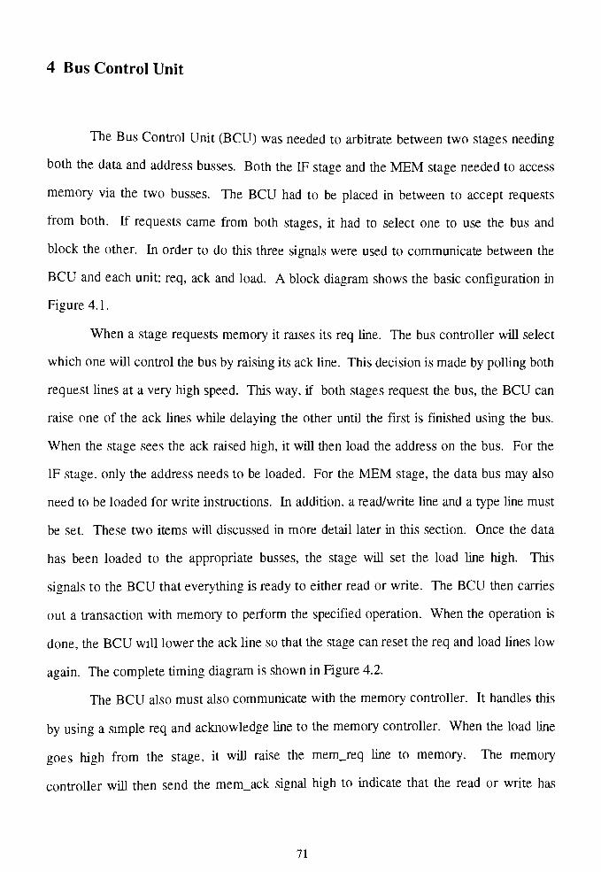
4 Bus Control Unit
The Bus Control Unit (BCU) was needed to arbitrate between two stages needing
both the data and address busses. Both the LF stage and the MEM stage needed to access
memory via the two busses. The BCU had to be placed in between to accept requests
from both. If requests came from both stages, it had to select one to use the bus and
block the other. Ln order to do this three signals were used to communicate between the
BCU and each unit: req, ack and load. A block diagram shows the basic configuration in
Figure 4. 1 .
When a stage requests memory it raises its req line. The bus controller will select
which one will control the bus by raising its ack line. This decision is made by polling both
request lines at a very high speed. This way, if both stages request the bus, the BCU can
raise one of the ack lines while delaying the other until the first is finished using the bus.
When the stage sees the ack raised high, it will then load the address on the bus. For the
IF stage, only the address needs to be loaded. For the MEM stage, the data bus may also
need to be loaded for write instructions. Ln addition, a read/write line and a type line must
be set. These two items will discussed in more detail later in this section. Once the data
has been loaded to the appropriate busses, the stage will set the load line high. This
signals to the BCU that everything is ready to either read or write. The BCU then carries
out a transaction with memory to perform the specified operation. When the operation is
done, the BCU will lower the ack line so that the stage can reset the req and load lines low
again. The complete timing diagram is shown in Figure 4.2.
The BCU also must also communicate with the memory controller. It handles this
by using a simple req and acknowledge line to the memory controller. When the load line
goes high from the stage, it will raise the mem_req line to memory. The memory
controller will then send the mem_ack signal high to indicate that the read or write has
71

begun. When the read has put the data onto the data bus, or the write has accepted the
data on the data bus, the mem_ack will be lowered, signifying that the operation is
complete. When this happens, the BCU will lower its mem_req as an acknowledgment to
the memory controller and the operation is complete. Figure 4.2 also shows the timing
diagram for the memory request between the BCU and the memory controller.
In order to implement the BCU, a finite state machine was used. This machine has
four states and is shown in Figure 4.3. State 0 represents a chance for the LF stage to
acquire the use of the bus. During this stage, if the LF's req line (ir) goes high, it gets the
rights to the bus. State 1 represents the same for the MEM stage. Therefore, if there are
no memory requests from either stage for a period of time, the machine will oscillate
between states 0 and 1 . State 2 represents the condition that the LF stage has control of
the bus. In order to leave this stage, the memory operation must be complete. State 3
represent the same for the MEM stage and, again, stays in this state until the memory
operation is complete. The schematic diagram of the bus control unit finite state machine
is given in Figure 4.4.
In order to save 4 lines running from the IF stage to the memory controller, the
MEM stage will be used to set the proper operation for the IF. The LF only performs a
load word operation to get the next instruction from memory. Therefore, when the MEM
stage is not using the bus, it will set the opcode line to "0x0 11", which signifies a word
operation, and the write line low to signify loading.
72

O)
o
o
Figure 4. 1 Schematic Diagram of the Bus Control Unit
73

s, I cvi
0
EV
1
to
E0)
E
3
Figure 4.2 Timing Diagram between of the BCU
74
State 0 : IF Stage can get control of the bus if it requests it
State 1 : MEM Stage can get control of the bus if it requests it
State 2 : IF Stage has control of the bus
State 3 : MEM Stage has control of the bus
4.3 States Used in the Bus Control Finite State Machine
75

lV
CD CDO C3
CX.
<
CO
o o
CD
C
JZ
O
(D
CD
CO
CO
CD
O
L.
C
o
CD
00
D
CO
Fisure 4.4 Schematic Diagram of the Bus Control Finite State Machine
76

5 Conclusions
This paper shows that there is a future in using asynchronous design techniques in
building a microprocessor. The machine designed in this thesis outperformed the
synchronous version in some areas; however, a complete performance evaluation could
not be obtained because memory was not implemented. For a typical program, the
performance was measured at around 10 MIPS. This number is generated by counting the
number of writeback pulses and dividing by the total time to complete a typical test
program. The layout occupied about 16 mm by 9 mm before the pads were placed.
There are four main advantages to asynchronous design. The first advantage is
that clock skew does not exist. The entire pipeline was shown to operate efficiently using
a handshaking controller to handle communication between sections. The overhead for
each section was shown to be 5.7 ns. Each section takes a variable amount of time to
complete. In the synchronous version, each section takes 20 ns to complete. For the
synchronous version, this is a significant overhead using a 2pm technology. As feature
sizes decrease however, the overhead should be reduced faster than the clock speed can be
increased.
The second advantage of asynchronous design is that the complexity of the system
will change as the feature size decreases. While the enormous global clock line will only
get more difficult to route and more difficult to handle clock skew, the HCC's will not
increase in complexity. In fact their speed will improve as more and more transistors are
packed onto a single chip since the gate capacitance loading will decrease. Ln addition, the
HCC's take very little area on the chip and consume very little power.
The third advantage of asynchronous design is the reduction of idle time at each
stage. In the synchronous version, the clock cycle time was dictated by the worst case
operation for every stage. This results in most instructions using only a portion of the
complete cycle. In the asynchronous version this is not the case. The pipeline stage can
77
go as fast as the previous section can supply data and the next section can consume the
data. General purpose microprocessors are ideal for this speed up improvement because
the time each instruction takes in a particular stage can vary greatly. For processors with
less deviation in timing at each stage, this improvement will not be as significant.
The final advantage of the asynchronous design methodology is that the data
dependency problem has been eliminated. By adding the dirty bit mechanism to the
registers, the asynchronous processor can execute consecutive data dependent
instructions. This advantage has one drawback. The performance will not be optimal
because the data dependent instruction still has to wait until the first instruction's data is
written back into the register; but it will be faster than the synchronous version where the
delay slot can contain a NOP. By giving the programmer the option of when to and when
not to use data dependencies, an optimization compiler can make a big difference in the
execution speed of a program.
While enjoying several advantages, asynchronous design also has several
disadvantages. The first disadvantage is that events can not be predicted. For designs that
only require local connection between adjacent blocks, this is not a problem. For this
design however, branch instructions require the first three stages to work. In the
synchronous version this is handled by implementing a two phase clock. For branches, the
LF can wait until the second phase of the clock to initiate an instruction fetch to allow the
ID decoder to decide whether the instruction is a branch. In the asynchronous version
however, the LF must be stalled until this decision is made. This makes the controlling
circuitry much more complex, because the order of operations is no longer simple to
enforce. Another example where this disadvantage occurs is in any instruction that saves
the link register. In the synchronous version, the first phase of the clock performs a simple
increment. If the previous instruction was a link instruction, that value was read off of the
PC and stored into the link register. In the asynchronous version this cannot be done
because the LF is running independently. It may be an instruction behind thus giving an
78
incorrect link value. This problem occurs any time either the flow of data goes backwards
in the pipeline or the flow of data does not involve adjacent sections. These instructions
usually take more time to complete because of the overhead involved to get the correct
order of operations. In contrast, all instructions that flow straight down the pipeline will
run faster because the instruction does not have to stall the pipeline at any stage.
The second disadvantage in asynchronous design involves generating the
completion signal. If the dummy delay method is used, the stage can not be tuned to its
maximum efficiency and also protect against the done signal going high too soon. The
dummy delay circuit also can not insure that the delay of the logic block will always match
the dummy delay. Factors such as time and temperature can result in the delay changing.
If the delay is not long enough, the next stage will latch the wrong data. If it takes too
long, efficiency will suffer. DCVSL alleviates this problem while causing others. The first
problem with DCVSL is that the area required for implementation is significantly higher.
For the adder circuit for example, the regular layout was roughly 60 percent the size of the
DCVSL block. This is due to the double rail signal propagation requirement of the logic.
Although the area used for individual transistors is roughly the same, the circuit uses twice
as many N transistors because both the function and its dual must be calculated. But the
circuit only uses only two P transistors to precharge the output. Because minimum
transistor sizes can be used in DCVSL and the total number of transistors is only slightly
larger, the resulting area is roughly the same. The reason for the increase in area is the
routing. It is much more complex and more lines must be routed.
One problem that became readily apparent in the layout step of this design was that
of ensuring the VHDL model represented the actual layout construction, since each step
was being done in parallel. In order to deal with this issue, all three of the designers that
participated in the project were in constant contact throughout the entire design cycle.
Complete top-down design could have remedied this problem by completing the VHDL
modeling at the behavioral, data flow and structural levels before any circuits were
79

designed. In this way, the design would be stable throughout the entire project. Many
times during this design, the VHDL modeling caught problems which required circuits and
layouts to be redone. The major cause of this problem was the requirement that each
thesis be made as independent as possible.
The design of the processor also suffered from the 2 pm process. This process is
very large by today's standards and accounted for the resulting size of the layout. This
fact and the incomplete implementation of the entire chip made this chip impractical to
fabricate. A future research project could be used to implement the memory support
features as well as complete exception handling support in order to fabricate the chip and
prove the concept in hardware. Another possible extension could be to resize the
transistors in the HCC to increase the speed.
All in all, asynchronous design may not be practical for today's high speed VLSI
designs because the overhead of the controller is still too large to account for gains in
speed it can achieve. However, the future looks bright as feature sizes decrease because
the overhead can be reduced. This paper also showed that a hybrid system using local
clocks may also be another solution too the clock problem. It has the advantages of
clocked design without the large capacitive loading that can slow down a globally
distributed clock.
80
6 Bibliography
Asada, Kunihiro, Okura Kazama, and Kyoung-rok Cho, "Design of a Self-timed Data Pathfor a Fully AsynchronousMicroprocessor", InternationalWorkshop SASLMI'92,
Kobe, Japan, 1992.
David liana, Ran Ginosar, Michael Yeoli, "An Efficient Implementation of Boolean
Functions as Self-Timed Circuits", IEEE Transactions on Computers, Vol. 41, No.
1, January 1992.
Dewilde, Prof. Dr. Ir. P. M., Dr. Ir. R. Nouta and Ir. M. Sim,"
A Self-Timed Handshake-
Scheme applied to a bit-serial multiplier", Technical Report 91-107, Delft
University of Technology, June 1991.
Ginosar, Ran, and NickMitchell, "On the Potential of Asynchronous Pipelined
Processors", Computer Architecture News, Vol. 18, No. 4, December 1990.
Hayes, John P., ComputerArchitecture and Organization, McGraw-Hill, New York,
1988.
Jacobs, Gordon M., and Robert Brodersen, "A fully Asynchronous Digital Signal
Processor Using Self-Timed Circuits", IEEE Journal ofSolid-State Circuits, Vol.
25, No. 6, December 1990.
Kane, Gerry, Heinrich Joe, MIPS RISCArchitecture, Prentice-Hall, New Jersey, 1992.
Mano, M. Morris, Computer Engineering Hardware Design, Prentice-Hall, New Jersey,
1988.
McAuley, Anthony J., Four State Asynchronous Architectures", IEEE Transactions on
Computers, Vol. 41, No. 2, February 1992.
Mukherjee, Amar, Introduction to nMOS and CMOS VLSI Systems Design, Prentice-Hall,
New Jersey, 1986.
Seitz, Charles I. "Self-Timed VLSI Systems", CalTech Conference on VLSI, January
1979.
Tan, Y. K. and Y. C. Lim, "Self-Timed System Design Technique", Electronic Letters,
Vol. 26, No. 5, March 1990.
81

Appendix A - List of Instructions
This section contains a list of all of the instructions that wereimplemented in this
processor. Figure A.l shows the complete list in Figure A.2 gives the decoding
information.
OP Description OP Description
Load/Store Instructions Multiply/Divide Instructions
LB Load ByteMULT Multiply
LBU Load Byte UnsignedMULTU Multiply Unsigned
LH Load Halfword DIV DivideLHU Load Halfword Unsigned DIVU Divide UnsignedLW Load Word
LWL Load Word Left MFHI Move From HI
LWR Load Word Right MTHI Move To HI
MFLO Move From LOSB
SH
Store Byte
Store HalfwordMTLO Move To LO
SW Store Word Jump and Branch Instructions
SWL Store Word Left J Jump
SWR Store Word Right JAL Jump And Link
Arithmetic Instructions JR Jump to Register
(ALU Immediate) JALR Jump And Link Register
ADDI Add Immediate BEQ Branch on Equal
ADDIU Add Immediate Unsigned BNE Branch on Not Equal
SLTI Set on Less Than Immediate BLEZ Branch on Less than or Equal to Zero
SLTIU Set on Less Than Immediate BGTZ Branch on Greater Than Zero
Unsigned BLT2 Branch on Less Than Zero
ANDI AND Immediate BGEZ Branch on Greater than or
ORI OR Immediate Equal to Zero
XORI Exclusive OR Immediate BLTZAL Branch on Less Than Zero And Link
LUI Load Upper Immediate
Arithmetic Instructions
(3-operand, register-type)
BGEZAL Branch on Greater than or Equal to
1 Zero And Link
ADD Add
ADDU Add Unsigned
SUB Subtract
SUBU Subtract Unsigned
SLT Set on Less Than
SLTU Set on Less Than Unsigned
AND AND
OR OR
XOR Exclusive OR
NOR NOR
Shift Instructions
SLL Shift Left Logical
SRL Shift Right Logical
SRA Shift Right Arithmetic
SLLV Shift Left Logical Variable
SRLV Shift Right Logical Variable
SRAV Shift Right Arithmetic Variable
Special instructions
SYSCAL System Call
BREAK Break
Figure A. 1 Complete List of InstructionsImplemented

R2000 Instruction Opcode Bit Encoding
31. .290
5. .30
1
2
3
4
5
6
7
20. .190
i
2
3
28. .26
0 1 2
Opcode3 4 5 - 6 7
SPECIAL BCOND J JAL BEO BNE BLEZ BOTZ i*
ADD1 ADD1U SLTI SLT1U AND1 OR1 XOR1 LUI
COP0 COP1 COP2 COP3 t t 1 r
t t T t t t t t
LB LH LWL LW LBU LHU LWR t
SB SH SWL SW t t SWR t
LWCO LWC! LWC2 LWC3 t T t t
SWCO SWC1 SWC2 SWC3 t t t t
2..0
0 1 2
SPECIAL3 4 5 6 7
SLL t SRL SRA SLLV t SRLV SRAV
JR JALR t t SYSCALL BREAK T t
MFHI MTHI MFLO MTLO t t T t
MULT MULTU D1V DIVU t t t t
ADD ADDU SUB SUBU AND OR XOR NOR
t t SLT SLTU t t t t
t t t t t t t t
t t t t t t T t
16. .16
0 1 2
BCOND3 4 5 6 7
BLTZ BGEZ
BLTZAL BGEZAL
Figure A.2 DecodingScheme used for the instructions
A2

Appendix B Various Files Used in the Project
Below is a summary of the miscellaneous files used in this project.
File 1 : multc - C program used to debug Booth's algorithm multipliction technique
File 2 : div.c - C program used to debug Booth's algorithm division technique
File 3 : inl.dat Instructer Decoder Espresso Input file #1
File 4 : in2. dat - Instructer Decoder Espresso Input file #2
File 5 : outl.dat - Instructer Decoder Espresso Output file #1
File 6 : out2. dat - Instructer Decoder Espresso Output file #2
File 7 : mem_dec.in Memory Decoder Espresso Input file
File 8 : mem_dec.out Memory Decoder Espresso Output file
File #1 - multc
Scott Siers
Program to simulate the operation of Booth's Algorithm
Multiplication Algorithm
mult . c
To run program Enter in both numbers in hex format and
specify whether the algorithm should be signed or unsigned
main ( )
{
int x, y;/* Input Numbers */
int sign;/* Input Sign */
int q, a, m, f, qp, i ;/* Various Registers */
int temp;/*
Temp variable */
/* Get Input Values */
printf ( "Enter first number > ");
scanf ("%x"
, &x) ;
printf ( "enter second number > ");
7
scanf ("%x"
, &y) ;
printf ( "Enter sign -->
"
B-l
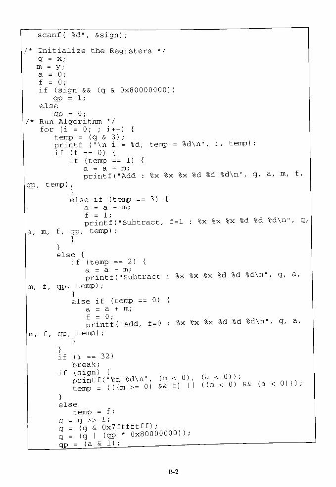
scanf ("%d", &sign) ;
/*Initialize the Registers */
q = x;
m = y;
a = 0;
f = 0;if (sign && (q & 0x80000000))
qp = 1;
else
qp = 0;/* Run Algorithm */
for (i = 0; ; i++) {
t emp = ( q & 3 ) ;
printf ("\n i = %d, temp =%d\n"
, i, temp);
if (f == 0) {
if (temp ==1) (
a = a + m;
printf ("Add : %x %x %x %d %d%d\n"
, q, a, m, i,
qp, temp) ;
}
else if (temp == 3) {
a = a-
m;
printf ("Subtract, f=l : %x %x %x %d %d%d\n"
, q,
a, m, f , qp, temp) ;
}
}else {
if (temp ==2) {
a = a-
m;
printf ("Subtract : %x %x %x %d %d%d\n"
, q, a,
m, f, qp, temp) ;
else if (temp == 0) {
a = a + m;
printf ("Add, f=0 : %x %x %x %d %d%d\n"
, q, a,
m, f , qp, temp) ;
}
}
if (i == 32)
break ;
if (sign) {nrintf("%d %d\n", (m<0), (a<0) ,
?emp = (((m >= 0 ) && f ) I I ( (m < 0) && (a < 0)));
}else
t emp= f ;
q = q 1;
a = (q & 0x7fffffff ) ;
q= (q I (qp
* 0x80000000));
qp= (a & 1) ;
B-2

a = a >> 1 ;
a = (a & Ox7fffffff ) ;
a = (a I (temp*0x80000000));
printf ( "Shift : %x %x %x %d %d %d\n", q, a, m, f, qp,
temp) ;
}
q = q 1;
q = (q & 0x7fffffff ) ;
q = (q I (qp*0x80000000) ) ;
printf ( "Answer : %x %x %x %d %d %d\n", a, q, m, f, qp,
temp) ;
}
File #2 - div.c
Scott Siers
Program to simulate the operation of Booth's Algorithm
Multiplication Algorithm
mult . c
To run program Enter in both numbers in hex format and
specify whether the algorithm should be signed or unsigned
I
main ( )
int q, a, m, s, Is, temp, i, sign;/* Registers */
/* Input Data */
printf ( "enter x --> ");
scanf ("%x"
, &q) ;
printf ( "enter y --> ");
scanf ("%x"
, &m) ;
printf ( "enter signed --> ");
scanf ("%d"
, &sign) ;
/* Initialize Variables */
a = 0;
Is = 0;
s = 0;
a = a-
ir^-
ls = (a < 0) ;
printf ("Subtract: i = %d, %x %x %x %d\n", i, q, a,
m, Is) ;
/* Start Algorithm */
for (i = 0; ; i++) {
if (Is == 0) {
B-3
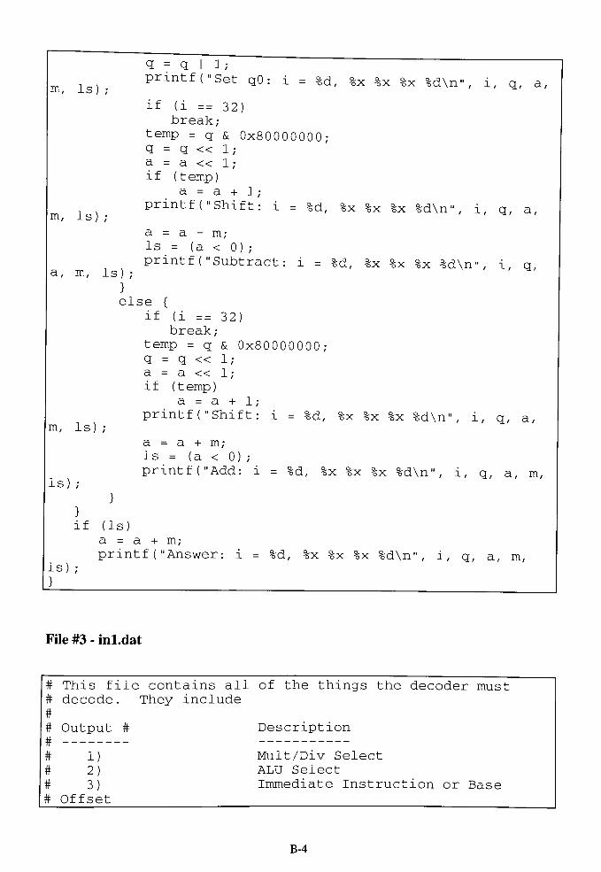
m, Is) ;
m, Is) ;
5 =
q I 1;printf ("Set qO : i = %d, %x %x %x %d\n", i, q, a,
if (i == 32)
break;
temp =
q & 0x80000000;q = q 1;a = a 1;if (temp)
a = a +1,-
printf ("Shift: i = %d, %x %x %x %d\n", i, q, a,
a = a-
m;
Is = (a < 0) ;
printf ("Subtract: i = %d, %x %x %x %d\n", i, q,a, m, Is) ;
}
else {
if (i == 32)
break;
temp = q & 0x80000000;q = q 1;a = a << 1 ;
if ( t emp )
a = a + 1 ;
printf ("Shift: i = %d, %x %x %x %d\n", i, q, a,m, Is) ;
a = a + m;
Is = (a < 0) ;
printf ("Add: i = %d, %x %x %x %d\n", i, q, a, m,Is) ;
}
}if (Is)
a = a + m;
printf ( "Answer: i = %d, %x %x %x %d\n", i, q, a, m,
Is);
}
File #3 - inl.dat
# This file contains all of the things the decoder must
# decode. They include
#
# Output # Description
#
# 1) Mult/Div Select
# 2) ALU Select
# 3) Immediate Instruction or Base
# Offset
B-4

File #4 - in2.dat
# This file contains all of the things the decoder must
# decode. They include#
# Output # Description# Z# D Mult/Div Select# 2) ALU Select# 3) Immediate Instruction or Base
# Offset
# 4) Branch (Conditional)# 5) Jump (Unconditional)# 6) Illegal Instruction
# 7) Test 1st Source Register Dirty# 8) Test 2nd Source Register Dirty# 9) Test Target Register Dirty# 10) Test HI Register Dirty# H) Test LO Register Dirty# 12) Exception (SYSCALL or BREAK)
#13) R - Register will contain address
# to jump to(JR or JALR)
#14) L - Link included with jump. (JAL
# or JALR)
# 15-16) Target Register Select
# Lines
# 00 Target gets Instruction lines 15:11
# 01 Target gets Instruction lines 20:16
# 10 Target gets all 0's
# 11 Target gets all l's (For Link
# instructions)
# 17) Branch Conditional and Link
#
.i 17
.o 17
type fr
.phase11111111111111111
000001 0000- 01010 0 10000 0 00 10 0
000001 0001- 1
000001 001-- 1 ______
000001 01--- i ______
000001 1000 01010 0 10000 0 00 11 1
000001 1001- i __---_
000001 101-- i ______
000001 11 i ______
000010 00001 0 00000 0 00 10 0
000011 01001 0 00100 0 01 11 0
oooio- 01010 0 11000 0 00 10 0
ooon- 01010 0 10000 0 00 10 0
ooi--- --- 01100 0 10100 0 00 01 0
01 i
B-6

innin0110 1010 0 00 01 0
"" "
" " -
onoo 0 10100 0 00 01 0
1001110110 1010 oi 0
10110------ HI
~~~
1100 1100 00 10 o
101111 ~-~-~-lZ___ ~Zl
0110 1100 io o
n ::: ::: --- i ::::: ::::::
File #5 - outl.dat
# This file contains all of the things the decoder must# decode. They include#
# Output # Description# Z
# D Mult/Div Select# 2) ALU Select
# 3) Immediate Instruction or Base# Offset
# 4) Branch (Conditional)# 5) Jump (Unconditional)# 6) Illegal Instruction
# 7) Test 1st Source Register Dirty# 8) Test 2nd Source Register Dirty# 9) Test Target Register Dirty# 10) Test HI Register Dirty# 11) Test LO Register Dirty# 12) Exception (SYSCALL or BREAK)
#13) R - Register will contain address
# to jump to(JR or JALR)
#14) L - Link included with jump. (JAL
# or JALR)
# 15-16) Target Register Select
# Lines
# 00 Target gets Instruction lines 15:11
# 01 Target gets Instruction lines 20:16
# 10 Target gets all 0's
# 11 Target gets all l's (For JAL
# instruction)
# 17) Branch Conditional Link Instructions
B-7

-o 17
#. phase 11111111111111111
.p17
000-01 00000100000000000
0010-1 01000000100001000001-1-
000001000000000000010--
000010100000100001-1-0-
000001000000000001-11--
00000100000000000
10--1 010000100000000001--1-
000000000010000001--0-
000000000100000001:L__ 0000000000010000001-- 00000010000000000
0--0 010000001000000001-1-- 00000100000000000
11 00000100000000000
00 01000001100000000
11 10000011011000000
1 01000011100000000
. e
File #6 - out2.dat
# This fil e contains all of the things the decoder must
#
#
#
#
#
decode . They include
Output #
1)
Description
Mult/Div Select
# 2) ALU Select
# 3) Immediate Instruction or Base
# Offset
# 4) Branch (Conditional)
# 5) Jump (Unconditional)
# 6) Illegal Instruction
# 7) Test 1st Source Register Dirty
# 8) Test 2nd Source Register Dirty
# 9) Test Target Register Dirty
# 10) Test HI Register Dirty
# 11) Test LO Register Dirty
# 12)Exception (SYSCALL or BREAK)
# 13) R - Register will contain address
# to jump to(JR or JALR)
# 14) L- Link included with jump. (JAL
# or JALR)
# 15-16) Target Register Select
# Lines
# 00 Target gets Instruction lines 15:11
# 01 Target gets Instruction lines 20:16
B-l-

* 1 Target gets all 0's
';11 Target gets all l's (For Link
jj instructions)
t 17) Branch Conditional and Link#
.i 17
.o 17
#. phase llllllllllllllin.p 15
1--111 000001000000000001-110 000001000000000000-000-1 000000000000000110-000 1 000001000000000000-000 1 000001000000000000-000--1 000001000000000000-0011 010000001000010100-010 000000010000000000-001 00001000000000100_1 000001000000000000-01 010100100000001001-1 01100011000000100
0-0-0 010100100000001000_i 01100010100000010
1-0 01100010100000010
. e
File #7 - mem decin
# This file contains all of the things the decoder must
#
#
#
decode. They include
Inputs
# 1-6 Opcode at Instruction 31-26
# 7 Sign bit at Data 31
# 8 Sign bit at Data 23
# 9 Sign bit at Data 15
# 10 Sign bit at Data 7
# 11 Address bit 1
#
#
#
#
#
12 Address bit 0
Output #
1)
Description
)tionMemory Excer.
# 2-5) VBT (3:0)
# 6) Store Instruction
# 7) Load Instruction
# 8-9) Shift Unit Se].ect 0 (1:0)
# 10-11) Shift Unit Select 1 (1:0)
B-9

I \\ }l\ Shift Unit Select 2 (1:0
1:0.I ^7 15) Shift Unit Select 3
l ^7 Mask Unit Select 3
l |G Mask Unit Select 2
I !q Mask Unit Select 1
I ;G Mask Unit Select 0'
^J) Sign extended bit (Or zero extended
bit for unsigned)
. i 12
o 20
type fr
.phase llllllllllllliiiini000000 --
0 1111 0 0 00 01 10 11 1111000001 --
0 1111 0 0 00 01 10 11 1111000010 --
0 0 0
000011 --
0 1111 0 0 00 01 10 11 11110001 0 0 0001 -
0 1111 0 0 00 01 10 11 111101 _
# Load Byte
100000 0 00 0 1111 0 1 11 01 01 01 1000 0100000 1 00 0 1111 0 1 11 01 01 01 1000 1
100000 -0 01 0 1111 0 1 10 00 00 00 0100 0100000 -1-- 01 0 1111 0 1 10 00 00 00 0100 1
100000 --0- 10 0 1111 0 1 01 00 00 00 0010 0100000 --1- 10 0 1111 0 1 01 00 00 00 0010 1
100000 0 11 0 1111 0 1 00 01 01 01 0001 0
100000 1 11 0 1111 0 1 00 01 01 01 0001 1
# Load Halfword
100001 0 00 0 1111 0 1 10 11 00 00 1100 0
100001 1 00 0 1111 0 1 10 11 00 00 1100 1
100001 01 1 _
100001 0- 10 0 1111 0 1 00 01 11 11 0011 0
100001 --1- 10 0 1111 0 1 00 01 11 11 0011 1
100001 11 1 _
# Load Word Left
100010 00 0 1111 0 1 00 01 10 11 1111 _
100010 01 0 1110 0 1 -- 00 01 10 -111_
100010 10 0 1100 0 1 -- -- 00 01 --11_
100010 11 0 1000 0 1 00 1 -
# Load Word
100011 00 0 1111 0 1 00 01 10 11 1111 -
100011 01 1 -
100011 1- 1 -
# Load Byte Unsi gnecI
100100 00 0 1111 0 1 11 01 01 01 1000 0
100100 01 0 1111 0 1 10 00 00 00 0100 0
100100 10 0 1111 0 1 01 00 00 00 0010 0
100100 11 0 1111 0 1 00 01 01 01 0001 0
# Load Halfword Unsigned
100101 00 0 1111 0 1 10 11 00 00 1100 0
100101 01 1 -
B-10

l^1 10 mi o 1 oo 01 n n oon o100101 n i# Load Word Right
100110 00 0 0001 0 1 11 -- -- -- 1--- -
100110 01 0 0011 0 1 10 11 11100110 10 0 0111 0 1 01 10 11 -- 111- -
100110 11 o 1111 0 1 00 01 10 11 1111 -
# Illegal Instruction100111
# Store Byte
101000 o io---- -- -- -
# Store Halfword
101001 00 0 io---- -- -- -
101001 -1 l ______ __
101001 10 0 io---- -- -- -
# Store Word Left
101010 0 io---- -- -- -
# Store Word
101011 0 io---- -- -- -
# Illegal Instructions10110-
______ __
# Store Word Right
101110 0 10---- --
# Illegal Instruction
101111 ______ __ __ _
# Illegal Instructions
H __ _ ______ __ __ _
File #8 - mem decout
# This file contains all of the things the decoder must
#
#
#
decode. They include
Inputs
# 1-6 Opcode at Instruction 31-26
# 7 Sign bit at Data 31
# 8 Sign bit at Data 23
# 9 Sign bit at Data 15
# 10 Sign bit at Data 7
# 11 Address bit 1
#
#
#
#
#
12 Address bit 0
Output #
1)
Description
DtionMemory Excei
# 2-5) VBT (3:0)
# 6) Store Instruction
# 7) Load Instruction
# 8-9) Shift Unit Select 0 (1:0)
# 10-11) Shift Unit Select 1 (1:0)
B-ll

J H ' Shift Unit Select 2 (1:0)
J i^7
5) Shift Unit Select 3 (1:0)* 16) Mask Unit Select 0
J 17) Mask Unit Select 1
J i8) Mask Unit Select 2
Ji9) Mask Unit Select 3
j[ 2) Sign extended bit (Or zero extended
# bit for unsigned)#
.i 12
.o 20
#. phase lllllllllllllliiini.p 25
0-0-1 10 000000000000000000010-0 100 00000000000000000001
1-0-11 1-10000000000000000000
0-11 1-00000000000000000001
0-1 1-0-00000000000000000001
0--1 11 000000000000000000010 1-01 00000000000000000001
1 01 1 100000000000000000001-011 00 000010111000000000101-0--1 1 10000000000000000000
01 0 001000000000001010001-001 01000010000000010000
1-011 01 00011011011000000110
1-1 00000100000000000000
1--01 01 00110000000011001100
1 1 1- 00000000011000000010
1-0-0 10 01111011000000000100
1-0-0 01 01111010100000001000
1-011 10 00111010110110001110
1 o- 00000000000101001000
1-0-0 11 01111011100000000010
1-0-0 00 01111010001010110000
01 00 00011000001101000110
1-011 11 01111010 0 01101111110
0 01111000001101111110
. e
B-12

Appendix C : Schematics of several cells used in the processor
This section gives several of the cells that were used as building blocks in the design.
Below gives a brief description of the cell along with its name. On the subsequent pages
will be the schematics. Appendix D will contain the corresponding layout for thesecells.
TRIBUF :
SR_LATCH :
REG :
CC :
LATCH :
BUFFER :
Tri-state buffer is used to allow multiple drivers on a bus line.
Used to latch in pulses from edge detectors
Edge triggered d flip-flop used as a memory element
Conditional Cell used in the Condition-Sum adder
Latch used to keep input constant for the entire stage
Buffer stase used as a driver circuit
C-l

D
O
A
.__ _L____
_-
A, c
r\j c\j
3 3
-
!-~ __
A
Figure C. 1 Schematic of a Tri-State Buffer
C-2

s
O
QZ
C3
r r\
v/ 7
Figure C.2 Schematic of an SR latch
C-3

d
o
Q_
CD
G)
W
Figure C.3 Figure of a d flip-flop
C-4

__J
ex CO CO CO
0)
(D
^ "\
V
\
I I
Fisure C.4 Schematic Diagram of the conditional cell
C-5

-A
G
i <!
G
G
Figure C.5 Schematic Diagram of a latch
C-6
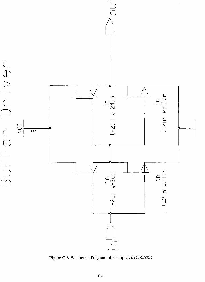
0
>
G
CJ
G
LO
O
2?C\J
II
Z5
(XJ
II
-, CO
CVI
II
II
ZJ
II
c
n
13
OvJ
Figure C.6 Schematic Diagram of a simple driver circuit
C-7

Appendix D : Layout of several cells used in the processor
This section gives several of the cells that were used as building blocks in the design.
Below gives a brief description of the cell along with its name.
TRLBUF:
SR_LATCH :
REG:
CC :
LATCH :
BUFFER :
Tri-state buffer is used to allow multiple drivers on a bus line.
Used to latch in pulses from edge detectors
Edge triggered d flip-flop used as a memory element
Conditional Cell used in the Condition-Sum adder
Latch used to keep input constant for the entire stage
Buffer stage used as a driver circuit
D-l

Figure D. 1 Layout of a Tri-State Buffer

tM
"-.''7.
^^i^t-_
lis i
rTiTTf,
-Si_i:
mm$8
!?
i;iqbar
r 7 .
H
:GI"
flpl'
r-riE
i
u'-A
: Snd
Figure D.2 Layout of an SR latch
D-3

c
:t_ (Gi
q
q*
:G
____;
:: ^-412}
i -)
H-
:{'_;
4-4-
ET
Is-
D
o
1_J
lipr
aJJ
I'
G
3
i-Bi
pm
? l
_J
>
3
a
m
P
a_
____
_7~7.;
I_J
s=
?
D
JIfe
Figure D.3 Figure of a d flip-flop
D-4

Figure D.4 Layout Diagram of the conditional cell
D-5

4 G,
-
t
~
a ,,;, ::.. |;S1 -
!~
} 3
:..fasTT-- '
....
Figure D.5 Layout Diagram of a latch
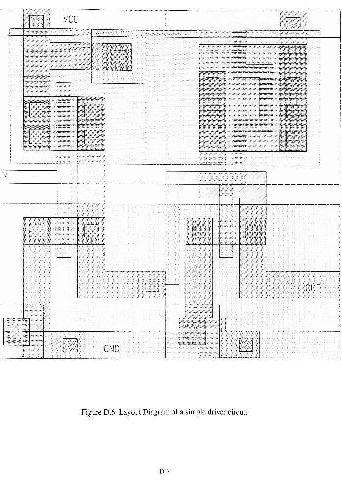
Figure D.6 Layout Diagram of a simple driver circuit
D-7