design and implementation of i2c communication protocol … · design and implementation of i2c...
TRANSCRIPT
International Journal of Scientific & Engineering Research, Volume 5, Issue 3, March-2014 ISSN 2229-5518
IJSER © 2014
http://www.ijser.org
Design and Implementation of I2C Communication Protocol on FPGA for EEPROM
Radha R C , Ravuri Aneesh Kumar
Abstract — The I2C protocol was given by Philips Semiconductors in order to allow faster devices to communicate with slower devices and also allow devices to communicate with each other over a serial data bus without data loss. We here present a model of I2C bus controller, the I2C controller is designed using Verilog HDL in Xilinx 12.2. The EEPROM, ADC and RTC will require an interface for communication between them. So I2C bus is used as an interface between them. So it is used to minimize system level interconnect. More over transmitting information over the I2C bus will improve system performance, since the transmission of digital data is much less susceptible to interference from environmental noise sources.
Index Terms — ACK, Address, Data, EEPROM (24C02), I2C, Master, Slave, Spartan-3E, Xilinx IDE.
—————————— ——————————
1 INTRODUCTION
I2C stands for Inter-Integrated Circuit. The I2C (Inter-
IC) bus protocol was developed by Phillips Electronics to a l-
low communication between integrated circuits (ICs) from
d ifferent manufacturers. Applications that use the I2C bus in-
clude microcontrollers, LCD, memory devices, PCs, cell-
phones, Television, ADCs, DACs and other devices.
It‟s I²C (Inter-Integrated Circuit, referred to as I-squared -C,
I-two-C or IIC [1].
The I2C bus uses two bid irectional signals, one as the serial
clock (SCL) line and other as the serial data (SDA) line. Each
device connected to the bus has a unique address used to iden-
tify the device in communication. The protocol is comprised of
a set of conditions to establish or terminate comm unication.
2 PROPOSED WORK
2.1 I2C COMMUNICATION PROTOCOL
The I2C is a synchronous protocol that allows a master device
to initiate communication with a slave device, then data is
exchanged between these devices.
2.2 SCL, SDA Lines
The I2C bus physically consists of 2 active wire connection.
The active wires, called SDA and SCL. SDA is Bi-d irectional
signal, SCL is uni-d irectional .
SDA is the „S‟erial „DA‟ta line
SCL is the „S‟erial „CL‟ock line
I2C is a Serial Interface and uses only the following two signals
to serially exchange data with another device.
SDA - Any data sent from one device to another goes on this
line.
SCL - It is generated by the master device and controls w hen
data is sent and when it is read .
2.3 Data Transfer
The data block represents the transfer of 8 bits of information.
The data is sent on the SDA line and SCL produces a clock.
The clock can be aligned with the data to ind icate whether
each bit is a “1” or a “0”. Data on SDA is only considered valid
when SCL is high. When SCL is not high, the data is permitted
to change. This is how the timing of each bit works. When
communicating to a I2C device, the 8 bits of data may be a
control code, an address or data. In this presentation we will
connect a serial EEPROM (24C02) to the bus and look at the
signals involved . Other I2C devices will require similar sig-
nals, but may not be identical.
The ACK and NACK condition. A device can “ACK”
or acknowledge a transfer of each byte by bringing the SDA
line low during the 9th clock pulse of SCL. The 9 bits of a trans-
fer look like this - 8 bits are clocked out for the data, then du r-
ing the 9th bit the item receiving the data grabs the bus for one
bit. If it d rives this bit low, then the device is sign aling an
“ACK”. Otherwise, it allows the SDA line to float high then it
is said to be not acknowlede “NACK”.
2.4 Masters and Slaves
The devices on the I2C bus are either masters or
slaves. A slave cannot initiate a transfer over the I2C
bus, only a master can do that.
There can be usually multiple slaves on the I2C bus,
however there is normally only one master. Both
master and slave can transfer data over the I2C bus,
but that transfer is always controlled by the master.
————————————————
Radha R C , Assistant Professor, Dept. of ECE, BMS College of Engg,
Bangalore, INDIA -560 019 .
E-mail: [email protected]
Ravuri Aneesh Kumar,M.Tech (Electronics), BMS College of Engg,
Bangalore, INDIA -560 019 .
E-mail: [email protected]
130
IJSER

International Journal of Scientific & Engineering Research Volume 5, Issue 3, March-2014
ISSN 2229-5518
IJSER © 2014
http://www.ijser.org
3 BLOCK DIAGRAM
Fig 3.1 : Block Diagram of Master and Slaves
4 I2C IMPLEMENTATION FOR EEPROM (24C02)
4.1 Initiation, Termination of Data
Fig 4.1 : Start and Stop Conditions [2]
Start Condition : SCL is high, SDA should be at fa lling edge
Stop Condition : SCL is high, SDA should be at rising edge.
4.2 EEPROM (24C02) Device Addressing
All I2C addresses are of either 7 bit or 10 bits. The use of 10 bit
addresses is rare and is not covered here. All of our modules
and the common chips you will use will have 7 bit addresses.
For an EEPROM(24C02) the 4 MSB‟s are fixed as “1010”, the
rest 3 bits are programmable, so we can connect maximum of 8
EEPROMS(24C02). When sending out the 7 bit address, we
still always send 8 bits. The extra bit is used to inform the
slave if the master is writing to it or read ing from it. If the bit
is zero(0) the master is writing to the slave. If the bit is one(1)
the master is read ing from the slave. The 7 bit address is
placed in the upper 7 bits of the byte and the Read/ Write
(R/ W) bit is in the LSB (Least Significant Bit).
Note : During transm ission of data bits in I2C, send right
from MSB to LSB during implementation using Verilog
HDL[3].
Fig 4.2 : Addressing Byte [4]
4.3 Writing Data to EEPROM(24C02) Device [4]
1. Send a start sequence
2. Send the I2C address of the slave with the R/ W bit low
(even address)
3. Send the internal register number in which you want to
write to
4. Send the data byte
5. [Optionally, send any further d ata bytes]
6. Send the stop sequence.
Fig 4.3 : Writing Sequence to Slave Module
4.4 Reading Data from EEPROM(24C02) Device
1. Send a start sequence
2. Send 0xC0 ( I2C address of the device with the R/ W bit
low (even address)
3. Send 0x01 (Any Internal address of the bearing register)
4. Send a start sequence again (repeated start)
5. Send 0xC1 ( I2C address of the device with the R/ W bit
high (odd address)
6. Read data byte from device
7. Send the stop sequence.
5 EEPROM’S
[6] Serial, 8-bit oriented , bi-d irectional data transfers can
be made at up to 100 kbit/ s the Standard -mode, up to 400
kbit/ s the Fast-mode, or up to 3.4Mbit/ s the High-speed
mode.
Features :
• Every EEPROM is enabled with I2C Communication
a Protocol
• Low -voltage and Standard -voltage Operation
(VCC = 2.7V to 5.5V)
• Internally Organized 128 x 8 (1K), 256 x 8 (2K),
512 x 8 (4K),1024 x 8 (8K) or 2048 x 8 (16K)
• Two-wire Serial Interface
• Bid irectional Data Transfer Protocol
• Write Protect Pin for Hardware Data Protection .
131
IJSER
International Journal of Scientific & Engineering Research Volume 5, Issue 3, March-2014
ISSN 2229-5518
IJSER © 2014
http://www.ijser.org
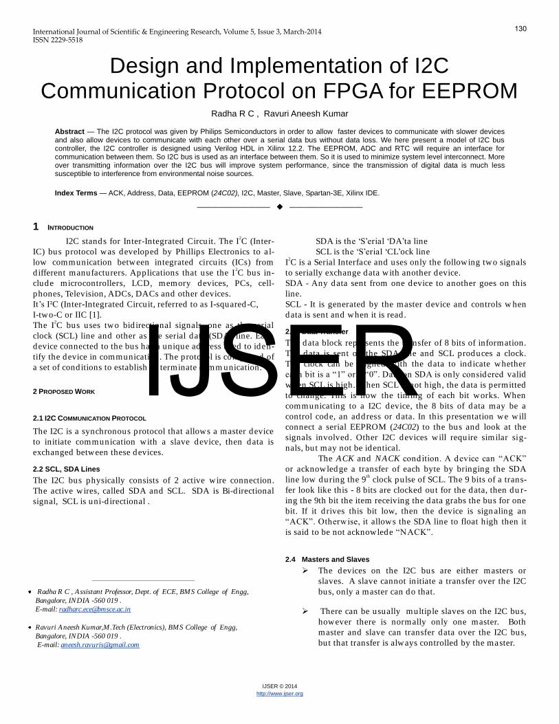
6 SIMULATION RESULTS
SIMULATION WAVEFORM OF WRITING DATA TO A EEPROM (24C02
SIMULATION WAVEFORM OF READING DATA FROM EEPROM (24C02)
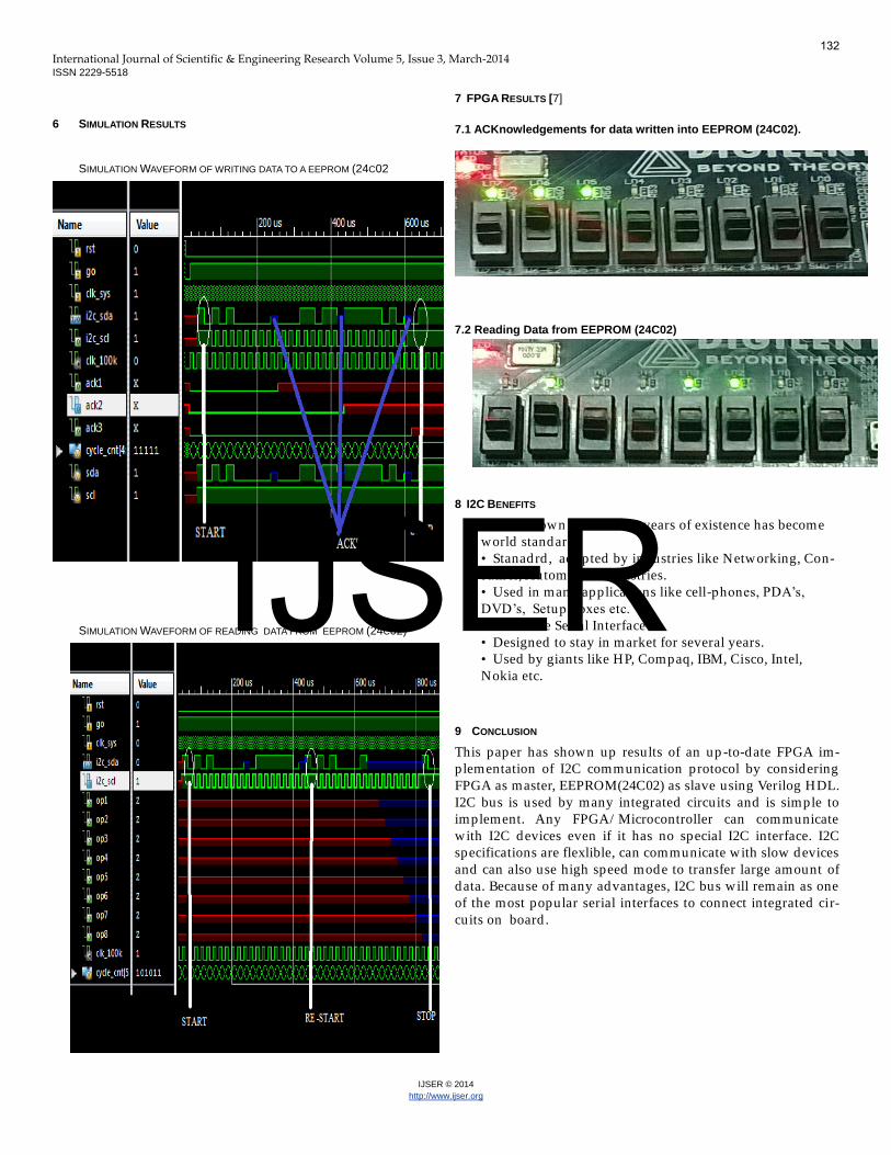
7 FPGA RESULTS [7]
7.1 ACKnowledgements for data written into EEPROM (24C02).
7.2 Reading Data from EEPROM (24C02)
8 I2C BENEFITS
• Well known bus over 20 years of existence has become
world standard .
• Stanadrd , adopted by industries like Networking, Con-
sumer, Automotive industries.
• Used in many applications like cell-phones, PDA‟s,
DVD‟s, Setup boxes etc.
• Two-wire Serial Interface
• Designed to stay in market for several years.
• Used by giants like HP, Compaq, IBM, Cisco, Intel,
Nokia etc.
9 CONCLUSION
This paper has shown up results of an up -to-date FPGA im-
plementation of I2C communication protocol by considering
FPGA as master, EEPROM(24C02) as slave using Verilog HDL.
I2C bus is used by many integrated circuits and is simple to
implement. Any FPGA/ Microcontroller can communicate
with I2C devices even if it has no special I2C interface. I2C
specifications are flexlible, can communicate with slow devices
and can also use high speed mode to transfer large amount of
data. Because of many advantages, I2C bus will remain as one
of the most popular serial interfaces to connect integrated cir-
cuits on board .
132
IJSER
International Journal of Scientific & Engineering Research Volume 5, Issue 3, March-2014
ISSN 2229-5518
IJSER © 2014
http://www.ijser.org
REFERENCES
[1] Frederic Leens, An Introduction to I2C and SPI Protocols,
IEEE Instrumentation and Measurement m agazine Febru-
ary 2009
[2] “Implementing I2C Communication Protocol in LAB-
VIEW FPGA”, http:/ / www.ni.com
[3] Samir Palnitkar,Verilog HDL - A guide to Digital Design
and Synthesis 2nd
ed ition, Sunsoft press
[4] I2C Tutorial “Using the I2C Bus”, http:/ / www.robot-
electronics.co.uk/ acatalog/ I2C_Tutorial.html
[5] AN10216-01 I2C MANUAL, Philips Semiconductors
March 24,2003
[6] Atmel Corporation. (2007) “AT24C02 Data Sheet” PDF
document
[7] “BasysTM
2 Spartan-3E FPGA Board” ,
http:/ / www.digilentinc.com
133
IJSER