design and implementation of neural network in fpga€¦ · design and implementation of neural...
TRANSCRIPT

Journal of Engineering and Development, Vol. 16, No.3, Sep. 2012 ISSN 1813- 7822
73
Design and Implementation of Neural Network in FPGA
Mrs. Rana D. Abdu-Aljabar
Assistance Lecturer
Information Engineering college / Nahrain University
Baghdad / Iraq
Abstract :-
This paper constructs fully parallel NN hardware architecture, FPGA has been used to
reduce neuron hardware by design the activation function inside the neuron without using
lookup table as in most researches, to perform an efficient NN. It consist of two main parts;
the first part covers network training using MATLAB program, the second part represents the
hardware implementation of the trained network through Xilinx high performance Virtex2
FPGA schematic entry design tools.
FPGAتصميم و تنفيذ الشبكة العصبية بواسطة
-: الخالصة
لتقليل المحتوى FPGAازية المتكاملة , و ذلك باستخدام هذا البحث يبني المحتوى الصلب للشبكة العصبية المتو
المادي المستعمل لتصميم الخلية العصبية و ذلك بتصميم الدالة الفعالة الموجودة داخل الخلية العصبية بدون استعمال
Lookup table .كما في غالبية االبحاث لكي نثبت فعالية الشبكة العصبية المقترحة
, اما الجزء الثاني فيشمل تنفيذ Matlabئين: الجزء االول يغطي تدريب الشبكة باستعمال برنامج البحث يحتوي جز
( بواسطة التصميم التخطيطي. Virtex2عالي االداء ) Xilinxالمحتوى المادي للشبكة المدربة باستعمال

Journal of Engineering and Development, Vol. 16, No.3, Sep. 2012 ISSN 1813- 7822
74
1- Introduction:-
Bio-inspired concepts such as neural networks, evolution and learning have attracted much
attention recently because of a growing interest in the automatic design of complex and
intelligent systems, capable of adaptation and fault tolerance. Engineers and computer scientists
have studied these biological concepts in an effort to replicate their desired qualities [1, 2] in
computing systems. Artificial neural networks (ANN) have found widespread deployment in a
broad spectrum of classification, perception, association and control applications [1]. The
aspiration to build intelligent systems complemented with the advances in high speed computing
has proved through simulation the capability of Artificial Neural Networks (ANN) to map, model
and classify nonlinear systems. Real time applications are possible only if low cost high-peed
neural computation is made realizable. Towards this goal numerous works on implementation of
Neural Networks (NN) have been proposed [2]. Artificial neural networks (ANNs) have been
mostly implemented in software. This has benefits, since the designer does not need to know the
inner workings of neural network elements, but can concentrate on the application of the neural
network. However, a disadvantage in real-time applications of software-based ANNs is slower
execution compared with hardware-based ANNs. [3]
Digital hardware-based implementations of ANNs have been relatively scarce, representive
examples of recent research can be found in. Recent advances in reprogrammable logic enable
implementing large ANNs on a single field-programmable gate array (FPGA) device. The main
reason for this is the miniaturization of component manufacturing technology, where the data
density of electronic components doubles every 18 months. ANNs are biologically inspired and
require parallel computations in their nature. Microprocessors and DSPs are not suitable for
parallel designs [4].
FPGA-based architectures offer high flexibility system design. Haitham K. and Esraa Z. [5]
describe hardware design of an artificial neural network on FPGA. A digital system architecture
is designed to realize a feedforward multilayer neural network. The designed architecture is
described using Very High Speed Integrated Circuits Hardware Description Language (VHDL)
and they use an equation which is a second order nonlinear function which has a tansig transition
between the upper and lower saturation regions, A fully parallel network is fast but inflexible.
Hanan A. and Firas R. [1] constructs fully parallel NN hardware architecture, training the
network using Particle Swarm Optimization (PSO) learning algorithm . Only Hardlimit activation
function for all network layers. The proposed learning algorithm was used for reducing the
neuron circuitry by lessining the multiplication process to only AND gates. Pearson [6] describe
an FPGA-based array processor architecture, which can simulate large networks. The processor
architecture is a single instruction path, multiple data path (SIMD) array processor and uses a

Journal of Engineering and Development, Vol. 16, No.3, Sep. 2012 ISSN 1813- 7822
75
bus-based communication protocol which limits its scalability. Suhap S., Yasar B., and Suleyman
Y. [7] The system architecture of NN is presented using VHDL and the sigmoid lookup table is
used in this paper . The network is implemented in Xilinx Spartan IIE. Ros [8] present an FPGA-
based hybrid computing platform. The neuron model is implemented in hardware and the
network model and learning are implemented in software.
Designing fully parallel modules can be available by ASICs and VLSIs but it is expensive and
time consuming to develop such chips. In addition the design results in an ANN suited only for
one target application. FPGAs not only offer parallelism but also flexible designs .The aim of this
work is to reduces neuron hardware to perform an efficient NN through the activation function
that designed inside the neuron without using lookup table module (LTM) as in many research
that use LTM . The network is implemented in Xilinx high performance Virtex2. The resultant
neural networks are modular, compact, and efficient and the number of neurons, number of
hidden layers and number of inputs are easily changed.
2- Artificial Neural Network (ANN) :-
An Artificial Neuron (AN) is a model of biological neuron. Where each AN receives signals from
the environment or other ANs, gathers these signals applying some activation function to the
signals sum and when fired transmits signal to all connected ANs. Input signals are inhibited or
excited through positive or negative numerical weights associated with each connection to AN
the firing of the AN and the strength of the exciting signal are controlled via a function referred
to as activation function. The AN collects all incoming signals and computes a net input signal as
a function of the respective weights. The net input serves to the activation function which
calculated the output signal of the AN. An ANN is a layered network of ANs. ANN may consist
of input, hidden and output layers. ANs in one layer are connected fully or partially to the ANs in
the next layer [1], as shown in Figure (1).
Fig 1. Neural network architecture.

Journal of Engineering and Development, Vol. 16, No.3, Sep. 2012 ISSN 1813- 7822
76
Following neuron model shown in figure (2) is widely used in artificial neural networks with
some variations.
Fig 2 . A single neuron example neural network.
X = Pj Wj + b …………(1)
Pj : is the input .
Wj : is the weight associated to each input .
X: is the summation of multiplying the input and the weight.
b : is the bais
y : is the neuron output.
3- Field Programmable Gate Array (FPGA) :-
The FPGA is especially designed IC that is often used for prototyping. Each FPGA has three
main parts; the Configurable Logic Block (CLB) is the most significant part. CLB provides
physical support for the program downloaded on FPGA. Another part is the Input Output Block
(IOB) which provides input and output for FPGA and makes it possible to communicate outside
the FPGA. The last part is the Programmable Interconnect (PI) which connects the different part
of FPGA and allows them to communicate with each other [9, 1] .
The choice to build a neural network in digital hardware comes from several advantages that are
typical for digital systems. Digital designs have the advantage of low noise sensitivity, and
weight storage is not a problem. With the advance in programmable logic device technologies,
FPGAs has gained much interest in digital system design [10]. Hardware realization of a Neural
Network (NN), to a large extent depends on the efficient implementation of a single neuron.
FPGA-based reconfigurable computing architectures are suitable for hardware implementation of
neural networks. FPGA realization of ANNs with a large number of neurons is still a challenging
task. [5]. FPGA are an excellent technology for implementing NNs hardware. Executing a NN on
FPGA is a relatively easy process. For lessening the design circuitry the training will be done
independently off line the FPGA, once the training is completed and the correct network weights

Journal of Engineering and Development, Vol. 16, No.3, Sep. 2012 ISSN 1813- 7822
77
is obtained these weights will be hard implied on FPGA. The accuracy in which these weights
can be coded will depends upon the number of bits existing to implement the weights. Parallelism
and dynamic adaption are two computational characteristics typically related with ANN FPGA -
based reconfigurable computing architecture are well suited to implement ANNs as one can
develop concurrency and rapidly reconfigure to adapt the weights and topologies of an ANN
[11]. FPGA realization of ANN with large number of neurons is still a not easy task because
ANN algorithm is wealthy with multiplication process and it’s relatively expensive to realize.
Various work reported in this area includes new multiplication algorithm for ANN, NNs with
some constraints to achieve higher speed of process at lower price and multichip realization
[1,12, and13].
4- Neural networks on FPGAs: specific assets:-
As stated above, FPGAs offer a cheap, easy and flexible choice for hardware implementations.
They also have several specific advantages for neural implementations:
1- Reprogrammable FPGAs permit prototyping: in most applications, several neural architectures
must be tested so as to find the most efficient one. This may be directly performed with the
hardware efficiency of an FPGA-based implementation, without any additional cost. Moreover a
good architecture that has been designed and implemented may be replaced later by a better one
without having to design a new chip.
2- On-chip learning is often considered as difficult and useless. Indeed it is used very seldom. But
on-chip learning usually results in a loss of efficiency in a hardware implementation, since it
requires some specific operators, a higher precision, . . . etc. Therefore off-chip learning is
naturally chosen when no dynamic learning is necessary. In a reconfigurable FPGA, on-chip
learning may be performed prior to a specific optimized implementation of the learned neural
network on the same chip.
3- FPGAs may be used for embedded applications, when the robustness and the simplicity of
neural computations is most needed, even for low scale productions.
4- FPGA-based implementations may be mapped onto new improved FPGAs, which is a major
advantage, considering that FPGA speeds and areas approximately double each year. Even large
neural networks may soon be implemented on single FPGAs, provided that the implementation
method is scalable enough. The FPGA concept is a major advance to ensure the scalability of
direct hardware mappings of neural networks .[14]
Journal of Engineering and Development, Vol. 16, No.3, Sep. 2012 ISSN 1813- 7822
78
5- The Proposed Design of neural network:-
The proposed design consists of neuron architecture design, activation function problem solving
and artificial neural network design which consist of three layers.
The initial parameters of the Neural Network used in the experiment are given below:
Type: Feed forward back propagation network
Number of layers: 3 (input, one hidden, and output layer)
Number of neurons in input layer : 4
Number of neurons in hidden layer : 4
Number of neurons in output layer : 1
Transfer function of the ith layer: Tansig
Training Function: Trainlm
Number of epochs used in training: 10000
Back propagation weight/bias learning function: learngdm
Error tolerance : 0.00000001
Performance function: Mean Square Error (MSE).
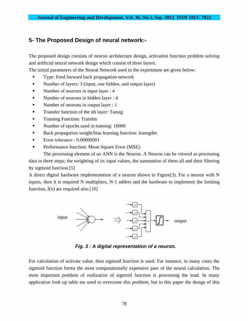
The processing element of an ANN is the Neuron. A Neuron can be viewed as processing
data in three steps; the weighting of its input values, the summation of them all and their filtering
by sigmoid function.[5]
A direct digital hardware implementation of a neuron shown in Figure(3). For a neuron with N
inputs, then it is required N multipliers, N-1 adders and the hardware to implement the limiting
function, f(x) are required also.[10]
For calculation of activate value, then sigmoid function is used. For instance, in many cases the
sigmoid function forms the most computationally expensive pare of the neural calculation. The
most important problem of realization of sigmoid function is processing the load. In many
application look up table are used to overcome this problem, but in this paper the design of this
input output
Fig. 3 : A digital representation of a neuron.

Journal of Engineering and Development, Vol. 16, No.3, Sep. 2012 ISSN 1813- 7822
79
activation function will be illustrated without using look up table for minimizing the hardware
design of single neuron.
The design of activation function is the second operation part of the neuron. The activation
function f(x) is used to limit the value of the neuron output. This activation function is given by
the following equation:
x-e1
1)(1
xF
….…..(2)
This equation was selected because it provides the necessary limiting of the outputs while having
some properties, which are useful in the learning phase of the algorithm.
Unfortunately, this equation contains the transcendental function (exponential term, exp), which
is somewhat difficult to calculate. Nordstrom and Svensson [15], list several functions, which
may be used as an approximation to the function used by McClelland and Rumelhart. These
functions all have the same general characteristics. They are continuously increasing, approach 0
at - and 1 at + , and have a continuous first derivative. The approximation that used in
this neural network is given by the following equation :
F2(x) =
1
12
1
x
x …. ….. (3)
The curves in figure(4) provide a similar limiting function. It is the general characteristics of the
sigmoid, not the precise equation which is important in this case.
In order to validate this activation function, the results are compared with sigmoid function as in
figure(4A) and those reported by Antony W. Savich, Medhat Moussa [16] as in figure(4B), In
this paper, a different approach for implementing the sigmoid function is adopted. It consists of a
linear approximation of (2). The formal mathematical representation of this approximation is
expressed by (4).
…….. (4)

Journal of Engineering and Development, Vol. 16, No.3, Sep. 2012 ISSN 1813- 7822
80
Fig.(4A):sigmoid function. Fig.(4B): Implementation of linear sigmoid
approximation function.
Fig. 4 : Sigmoid activation function.
The agreement is found to be acceptable which validates the present activation function .The
above figure (4A) shows the output curve of the two function (F1(x) , F2(x) ). This shows that the
two function is the same function [17].
Since the final result of this equation f(x) is a digital circuit. This circuit takes as its input a value
x which represent the result of sum of product, and returns the output f(x). The functional units
used by the circuit are : two adders, a divider, an absolute value and a divide-by-two circuit.
Some simple optimizations have been performed on this circuit. Once the circuit for this function
has been extracted, it may be used as a macrocell, much like the other macrocells in the circuit.
6- Implementation of Suggested Design:-
The implementation of this neural network algorithm is well suited to an FPGA . The first step is
to design the equation [ x
x
1 ] from equation (3) and getting its result then complete the design
of all sigmoid function. The design of equation [ x
x
1 ] requires the divider circuit and the
absolute circuit to output the result of the summation in the first operation part of the neuron. The
block diagram of single neuron is shown in figure (5).

Journal of Engineering and Development, Vol. 16, No.3, Sep. 2012 ISSN 1813- 7822
81
The activation Block in Figure(5), which performs the multiplications Pj wj and the summation of
these multiplied terms as in Equation (1), is always on the neuro-chip (or the processing element
of the neurocomputer). The data flow between these blocks is controlled by the Control Unit that
is always on the chip. The control parameters are used for controlling the hardware by a host. The
data flow is such that the weights from the Weights Block and the inputs from outside or from the
outputs are multiplied and the products are summed in the Activation Block, then the outputs are
obtained in the Neuron State Block from the transferred sum of the products [17]. Neuron states
and weights can be stored in digital form. Weights can be stored in registers if it is little numbers
of weights or stored in ROM . Then the complete design of the neuron has been done to create
the top of the hierarchy level as shown in figure (6).
Weighs
Block
Control
unit
Activation
Block Transfer
Function
Block
Neuron
State
Block
Control Parameters
Weights
Inputs
Output
clock
clear
enable
Fig. 5: The Block diagram of the neuron.

Journal of Engineering and Development, Vol. 16, No.3, Sep. 2012 ISSN 1813- 7822
82
Fig. 6 : The micro Block of the neuron.
Figure(7) shows the total design flow using MATLAB and Xilinx . The MATLAB program
consists of the built and learning programs of NN . After the leaning procedure, weights data are
fixed and saved to a file. Then transmit the weights to the Xilinx.
The complete hardware design of the circuit of the neural network which contains the neuron
and the inputs and output of each neuron and the input signal, weights and bias registers for each
neuron is as. shown in figure(8). This neural network was built as a separate neural network each
neuron as a micro neuron.
MATLAB (Learning)
NN
Learning
Save
Weight
s
Input data
Xilinx (complete design)
Registors
(weights)
Hardware
NN
Output
data
Fig. 7: Design environment

Journal of Engineering and Development, Vol. 16, No.3, Sep. 2012 ISSN 1813- 7822
83
fig. 8 : The complete hardware design of the neural network

Journal of Engineering and Development, Vol. 16, No.3, Sep. 2012 ISSN 1813- 7822
84
7- Result:-
In MATLAB program the network undergoes process of training, continuously in an iterative
manner it calculates output from each layer, extracting the mean square error and propagating it
backwards if it is not approaching targets. Due to this backward error propagation, error-signal
for each neuron is calculated. Which in fact is used for neuron weight updating. If its approaching
targets then training is considered done. In this way network approaches the set known correct
outputs (targets) in order to be trained. The process of training is shown in Figure(9), in which
training curve is approaching its goal through readjustment of weights and biases.
Fig. 9 : Training the neural network.
When this training is completed as in figure(9), the program gives the final weights that are
connected between neurons and also the final bias values that are connected to these neurons ,
these weights and bais converted to hexadecimal number. The final weights and bais are in
table(1) and there are represented in hexadecimal form, these values of weights and biases are
needed in complete hardware design of the neural network in the implementation using the
FPGA.

Journal of Engineering and Development, Vol. 16, No.3, Sep. 2012 ISSN 1813- 7822
85
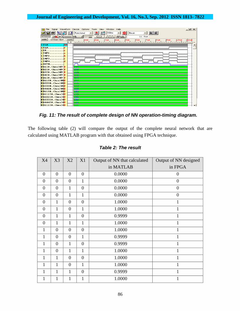
The result of FPGA , for the neuron that built above, and after specified input values of the
weights, and the input values of ( I ) as an input to the neuron, and then test of operation of the
neuron was shown in figure (10). Then figure (11) shows the complete operation result of the
total neural network
Fig. 10 : The result of single neuron operation-timing diagram.
Table 1: The weights and bias of each neuron.
Journal of Engineering and Development, Vol. 16, No.3, Sep. 2012 ISSN 1813- 7822
86
The following table (2) will compare the output of the complete neural network that are
calculated using MATLAB program with that obtained using FPGA technique.
Table 2: The result
X4 X3 X2 X1 Output of NN that calculated
in MATLAB
Output of NN designed
in FPGA
0 0 0 0 0.0000 0
0 0 0 1 0.0000 0
0 0 1 0 0.0000 0
0 0 1 1 0.0000 0
0 1 0 0 1.0000 1
0 1 0 1 1.0000 1
0 1 1 0 0.9999 1
0 1 1 1 1.0000 1
1 0 0 0 1.0000 1
1 0 0 1 0.9999 1
1 0 1 0 0.9999 1
1 0 1 1 1.0000 1
1 1 0 0 1.0000 1
1 1 0 1 1.0000 1
1 1 1 0 0.9999 1
1 1 1 1 1.0000 1
Fig. 11: The result of complete design of NN operation-timing diagram.

Journal of Engineering and Development, Vol. 16, No.3, Sep. 2012 ISSN 1813- 7822
87
Table1 shows the compression of the output of neuron in MATLAB program and the FPGA. This
output is the same as MATLAB result in the above example and is equal to the desired output.
Therefore, this result shows the right operation of NN-FPGA.
9- Calculation Unit Hardware Architecture:-
The explained functions are performed by the following logical circuits of the calculation unit:
Table (3) lists the chip area occupation for this design. This report is created during synthesize
stages.
Table 3 : Device Utilization Summary for design NN.
Device type
Percentage area occupied
Number of Slices 1,726 out of 5,120 33%
Number of Slices Flip Flops 3,113 out of 10,240 30%
Number of bonded IOBs 233 out of 328 71%
Number of 4 input LUTs 1,372 out of 10,240 13%
Total equivalent gate count for design 40,731
Number of RPM macros 36
The complete right implementation of the neural network is shown in figure (12), which shows
the complete stages of implementation of neural network using FPGA and how each stage
completes with out error.
Fig. 12 : The flow engine of the circuit.

Journal of Engineering and Development, Vol. 16, No.3, Sep. 2012 ISSN 1813- 7822
88
10- Conclusion and Suggestion:-
This paper constructs fully parallel NN hardware architecture reduces neuron hardware to
perform an efficient NN through the activation function that designed inside the neuron without
using LTM. This design was performed using Schematic editor tools in reconfigurable device
(FPGA) program. The neural network description is modular, being possible to easily increase or
decrease the number of neurons. The description in the synchronous mode allowed us to exploit
this modularity and to maintain the accuracy of the results of the neural network. The resultant
neural networks are modular, compact, and efficient and the number of neurons, number of
hidden layers and number of inputs are easily changed the choice of dynamic range, precision
and arithmetic hardware architecture used in neural networks application has a direct impact on
the processing density achieved. Using suitable precision arithmetic design, one can be achieve
adequately high speed and small size for real time ANNs implementations.
References:-
[1] Assist. Prof. Dr. Hanan A. R. Akkar, 2M. Sc. Student Firas R. Mahdi , “
Implementation of Digital Circuits Using Neuro - Swarm Based on FPGA “,
International Journal of Advancements in Computing Technology Volume 2, Number
2, June, 2010 .
[2] John Wiley & Sons Ltd, “Computational Intelligence: An Introduction” , A. P.
Engelbrecht, 2007.
[3] F Morgan 1, S Cawley 1, B Mc Ginley 1, S Pande 1, LJ Mc Daid2, B Glackin2, J
Maher1, J Harkin2 , “Exploring the Evolution of NoC-Based Spiking Neural Networks
on FPGAs”, Bio-Inspired Electronics and Reconfigurable Computing Research Group
(BIRC), National University of Ireland, Galway, 2010.
[4] M.T. Tommiska, “Efficient Digital Implementation of the Sigmoid Function for
Reprogrammable Logic”, IEEE Proceedings, Computers and Digital Techniques, vol.
150, no. 6, pp. 403- 411, 2003.
[5] Haitham Kareem Ali and Esraa Zeki Mohammed “Design Artificial Neural Network
Using FPGA”IJCSNS International Journal of Computer Science and Network
Security, VOL.10 No.8, August, 2010
Journal of Engineering and Development, Vol. 16, No.3, Sep. 2012 ISSN 1813- 7822
89
[6] M. Pearson, “Implementing SNNs for Real-Time Signal- Processing and Control
Applications: A Model-Validated FPGA Approach”, IEEE Trans. on Neural Nets, vol.
18, no. 5, 2007
[7] Suhap Sahin, Yasar Becerikli*, and Suleyman Yazici , ”Neural Network
Implementation in Hardware Using FPGAs” , Springer-Verlag Berlin Heidelberg 2006
.
[8] E. Ros., “Real-Time Computing Platform for Spiking Neurons (RT-Spike)”, IEEE
Transactions on Neural Networks, vol. 17(4), 2006.
[9] R. Raeisi and A. Kabir, “Implementation of Artificial Neural Network on FPGA”,
American Society for Engineering Education, Indiana and North Central Joint Section
Conference, 2006.
[10] Steven A. Guccione and Mario J. Gonzalez ″ A Neural Network Implementation
Using Reconfigurable Architectures″ Department of Electrical and Computer
Engineering, The University of Texas at Austin , USA, 1994.
[11] A. Muthuramalingam, S. Himavathi and E. Srinivasan, “Neural Network
Implementation Using FPGA: Issues and Application”, International Journal of
Information Technology, Vol. 4, No. 2, PP 86-92.
[12] R. H. Turner, R. F. Woods, “Highly efficient limited range multipliers for LUT- based
FPGA architecture”, IEEE transactions on vary large scale integration system Vol. 15,
No.10, 2004, PP 1113-1117.
[13] B. Noory and V. Grozo, “A Reconfigurable Approach to Hardware Implementation
of Neural Network”, Canadian conference on Electrical and Computer Engineering
IEEE, CCGE1, 2003, PP1861-1863
[14] Amos R. Omondi , Jagath C. Rajapakse, “FPGA Implementations of Neural
Networks” , Flinders University, Adelaide, SA, Australia, Nanyang Tecnological
University, Singapore , Published by Springer, P.O. Box 17, 3300 AA Dordrecht, The
Netherlands , © 2006 Springer
[15] Nordstrom, T. and Svensson, B. " Using and Designing Massively Parallel Computers
for Artificial Neural Networks" Journal of Parallel and Distributed Processing, no.3,
pp. 260-285, March 1998.
[16] Antony W. Savich, Medhat Moussa, and Shawki Areibi ,”The Impact of Arithmetic
Representation on Implementing MLP-BP on FPGAs: A Study” , IEEE
TRANSACTIONS ON NEURAL NETWORKS, VOL. 18, NO. 1, JANUARY 2007 .

Journal of Engineering and Development, Vol. 16, No.3, Sep. 2012 ISSN 1813- 7822
90
[17] Steven A. Guccione and Mario J. Gonzalez ″ A Neural Network Implementation
Using Reconfigurable Architectures″, Department of Electrical and Computer
Engineering, The University of Texas at Austin , USA, 1994.
[18] Yihua Liao , “Neural Networks in Hardware: A Survey”, Department of Computer
Science, University of California, Davis One Shields Avenue, Davis , 1999
[19]Hossein Sahoolizadeh, Ahmad Keshavarz, “A FPGA Implementation of
Neural/Wavelet Face Detection System”, Australian Journal of Basic and Applied
Sciences, 4(3): 379-388, 2010 , ISSN 1991-8178 , © 2010, INSInet Publication.
[20] Basma M. K. Younis, Basil Sh. Mahmood, Fakhraldeen H. Ali, “Reconfigurable Self-
Organizing Neural Network Design and it's FPGA Implementation”, Technical
Engineering College College of Electronics Computer Engineering Department ,In
Mosul University of Mosul University of Mosul , June 2009.
[21] Nasri Sulaiman, Zeyad Assi Obaid, M. H. Marhaban and M. N. Hamidon, “Design
and Implementation of FPGA-Based Systems - A Review”, Australian Journal of Basic
and Applied Sciences, 3(4): 3575-3596, 2009 , ISSN 1991-8178,Malaysia , © 2009,
INSInet Publication.
[22] Aydoğan Savran, Serkan Ünsal, “Hardware Implementation of a Feedforward Neural
Network Using FPGAs’, Ege University, Department of Electrical and Electronics
Engineering, 2003.
[23] Indranarain Ramlall , “Artificial Intelligence: Neural Networks Simplified”
University of Technology, Mauritius , International Research Journal of Finance and
Economics - Issue 39 (2010)