design and implementation of quasi planar ka band array ...833606/fulltext01.pdf · design and...
TRANSCRIPT
Design and Implementation of
Quasi Planar K-Band Array
Antenna Based on Travelling
Wave Structures Zunnurain Ahmad
This thesis is presented as part of Degree of
Master of Science in Electrical Engineering with emphasis on
Radio Communications
November 2012- May 2013
Department of Electrical Engineering
Supervisors at Fraunhofer IIS: Dr.-Ing. Mario Schühler /Dipl.-Ing. Hans Adel
Supervisors at University: Prof. Dr.-Ing. Hans-Jürgen Zepernick / Dr. Sven Johansson

ii
(page intentionally left blank)

iii
ABSTRACT
Designing antenna arrays based on travelling wave structures has been studied
extensively during the past couple of decades and literature on several array topologies is
present. It has been an active area of research as constant improvement of antenna arrays is
desired for different communication systems developed. Slotted waveguide antennas are one
form of travelling wave structures which is adapted in this study due to several advantages
offered over other planar array structures. Waveguide slots have been used for a couple of
decades as radiating elements. Several design studies have been carried out regarding use of slots
with different orientations and geometry and cascading them together to be used as array
antennas. Waveguide antennas are preferred as they provide low losses in the feed structure and
also offer good radiation characteristics.
This study provides a design procedure for implementing a circular polarized planar
antenna array based on slotted waveguide structures. The antenna is designed to work in the 19.7
- 20.2 GHz range which is the operating frequency for the downlink of satellites.

iv
(page intentionally left blank)

v
Acknowledgements
First of all, I would like to express my gratitude towards Dr. Mario Schühler for providing
me with an opportunity to work on this research activity at Fraunhofer Institute of Integrated
Circuits and for his guidance throughout the duration of my stay, also I want to mention the
support of my second supervisor Dipl.-Ing. Hans Adel at Fraunhofer IIS who was a major source
of inspiration and motivation during the thesis activity and the discussions made with him proved
quite helpful. I also appreciate the support of Dr. Sven Johnsson and Prof. Dr.-Ing. Hans-Jürgen
Zepernick who accepted to be my internal supervisors at BTH.
Zunnurain Ahmad
Erlangen, Germany

Table of Contents Table of Contents ......................................................................................................................... vi
Chapter 1
Introduction ................................................................................................................................... 1
1.1 Aim of thesis .................................................................................................................... 1
1.2 Structure of thesis ............................................................................................................. 2
1.3 Background of Slotted Waveguide Antennas .................................................................. 3
1.4 Linear Polarized Antenna Arrays ..................................................................................... 7
Chapter 2
Design of Circular Polarized Antenna Structures ................................................................... 10
2.1 Circular Polarized Slots .................................................................................................. 10
2.2 Single Slot Characterization ........................................................................................... 12
2.3 X-Slots ............................................................................................................................ 13
2.4 Offset Compound Slot Pair ............................................................................................ 15
Chapter 3
Linear Array Design ................................................................................................................... 18
3.1 Design Procedure ........................................................................................................... 20
3.1.1 Grating lobe problem .............................................................................................. 20
3.1.2 Dimensions of Waveguide ...................................................................................... 23
3.2 Linear Array Design ....................................................................................................... 26
3.2.1 Cross Slot Design .................................................................................................... 26
3.2.2 Offset Compound Slot Structure ............................................................................. 30

vii
Chapter 4
Waveguide to Microstrip Transition at 20 GHz ...................................................................... 48
4.1 Existing Designs ............................................................................................................. 49
4.2 Design of Microwave to Waveguide Transition ............................................................ 50
Chapter 5
Planar Array Design ................................................................................................................... 57
Chapter 6
Measurement Results .................................................................................................................. 64
6.1 Fabrication of the Linear Array ...................................................................................... 64
6.2 Measurements ................................................................................................................. 67
6.3 Radiation Characteristics ................................................................................................ 70
Chapter 7
Conclusion and Future Work .................................................................................................... 74
References.....................................................................................................................................76

viii
List of Abbreviations
MoM (Method of Moments)
EM (Electro Magnetic)
CNC (Computer Numeric Control)
AUT(Antenna Under Test)
RHCP (Right Hand Circularly Polarized)
LHCP (Left Hand Circularly Polarized)
CST (Computer Simulation Technology)
HFSS (High Frequency Structural Simulator)
PCB (Printed Circuit Board)

ix
(page intentionally left blank)

Chapter 1: Introduction
1
Chapter 1
Introduction
1.1 Aim of thesis
New perspectives in satellite communications have been explored in recent years and
establishing high speed links from satellite to ground stations antennas plays an important role.
Specific antenna designs have to be considered when stations are mobile. The requirements of
antennas are strict in this case as characteristics such as being of low profile and having short
electrical length are to be achieved.
Possibilities of new mobile communications in the Ka band frequency range (uplink at
29.5…30.0 GHz and downlink at 19.7…20.2 GHz) have been studied [1] and a need exists to
design efficient antenna systems which fulfill the demands of mobile and nomadic terminals.
Commonly used solutions such as parabolic reflector antennas exist in the market which provide
high directivity and good polarization purity but suffer from drawbacks such as mechanical
height which is not suitable for mobile terminals.
The main focus of the thesis is therefore the design of a planar array antenna based on
travelling wave structures which has a lower mechanical height. The advantages of these

Chapter 1: Introduction
2
structures are compactness in size and have a conformal installation ability which proves them to
be an ideal choice for mobile terminals. Slotted wave guide array topologies were studied and it
was decided to adopt these structures for the array design. Slotted waveguides seem to exhibit
relatively low losses in the feeding network. Their applications have been found in high power
and planar array structures, especially for use in aircrafts, where size is an important issue.
Figure 1.1 shows the application of the planar antenna array, which is to be mounted on the roof
of a mobile station and communicates with the satellite, having a specific angle of elevation with
earth’s curvature.
Figure 1.1 Mobile to Satellite Communication.
1.2 Structure of thesis
Having provided the problem statement and aim of the thesis, a thorough study on the
configurations of the waveguides was conducted. Designs that have already been presented in the
literature were investigated and initial simulations were performed. The main focus of the thesis
is on practical development of slotted waveguide structures with design guidelines rather than
proceeding with intensive theoretical and mathematical investigations on slotted waveguide
structures. Mathematical analysis of fields propagating inside various slot structures has already
been presented in literature [2] [3] [4]. In the next section, a brief theory of slotted waveguide is

Chapter 1: Introduction
3
given. The report is comprised of seven chapters and a summary of the chapters is given as
follows.
Chapter 2: This chapter presents an overview on how to achieve circular polarization from
different slot configurations and a discussion on the type of slot structures and their performance.
Chapter 3: In this chapter, a detailed design procedure is presented on how a linear array
configuration can be done. A design based on both cross slot and offset compound slot is
presented and their radiation characteristics are discussed. Furthermore, a guideline for design of
a circular polarized linear antenna array for 20 GHz is presented.
Chapter 4: This chapter discusses about the design of a waveguide to Printed Circuit Board
(PCB) transition. It discusses about different solutions that are available and the most efficient
design that can be adopted which provides a good transition at 20 GHz and also provides a low
insertion loss.
Chapter 5: The design of a planar array is presented and a discussion is given about the
configuration in which the array is arranged and how to scan the angle in the elevation plane by
feeding the individual linear arrays by progressive phase shift. The limitations about the scan
angle are also discussed.
Chapter 6: The aim of the chapter is to provide the measurement results obtained after
manufacturing the antenna. A comparison of simulation and measurement results is provided.
Chapter 7: Conclusions about the array design are drawn and guidelines for future study are
pointed out through which the existing design can be further enhanced.
1.3 Background of Slotted Waveguide Antennas
Slotted waveguide array antennas have been studied for a couple of decades. Major
contributions were made by Sangster [12] and Elliot [5]. Different slot structures were tested for
applications in array antennas. Waveguide slot antennas are by nature of very low profile and
Chapter 1: Introduction
4
tend to provide a good radiation in broad side direction. Further advantages of these structures
are that they exhibit geometric simplicity, efficiency and polarization purity.
A waveguide slot is just a slot cut into the broad wall or edge of a waveguide. The use of
Computer Numeric Control (CNC) machines makes it possible to mill out the slot structures
precisely. A narrow slot milled out along the center line of the waveguide broad wall does not
radiate and must be rotated about the center line or displaced towards the edge. These slot
structures exhibit an equivalent circuit, for instance, a displaced slot from the center line is
equivalent to shunt admittance across the feed line and the rotated inclined slot is equivalent to a
series slot [2].
Several topologies of a slot structures have been investigated by scientists over the
previous years and detailed analysis on slots have been performed investigating the effects of slot
admittances and couplings. Figure 1.2 shows some of the slot structures present in literature [3].
Figure 1.2 Slot Topologies.
Slot a represents a longitudinal shunt slot, which is offset from the center line.
Slot b is regarded as center inclined slot.

Chapter 1: Introduction
5
Slot c is regarded as a series slot.
Slot d is cut in the narrow side of the waveguide and represented by series admittance. The slots
seen in the figure each have an own equivalent circuit as discussed earlier which can be seen in
Figure 1.3.
When a slotted waveguide is excited with the Transverse Electric ( ) mode, the fields
propagating inside the waveguide are given by equations:
( )
(1)
( ) (2)
( ) ( )
where E and H define the electric and magnetic fields, denotes the wave number and
denote the respective direction of the fields in the coordinate system. is magnitude
of the E field. is the permeability of free space and = 2πf. f defines the frequency.
Chapter 1: Introduction
6
G jB
Longitudinal Slot
G jB
G jB
Center Inclined Slot
Narrow Wall Slot
Figure 1.3 Equivalent Impedance Representations for Longitudinal, Center Inclined and
Narrow Wall Slot.
These equivalent circuit representations can be used for the slots to determine the overall
slot impedance and computing the mutual coupling effects between slots. The study by
Stevenson [4] focused towards computation of slot characteristics keeping in reference following
points:
Narrow slots.
Slot length equal to half free-space wavelength.
Perfectly conducting thin wall and perfect conducting ground plane of infinite extent.
Chapter 1: Introduction
7
Taking these factors into account, extensive calculations were applied to derive the
values of resonant resistance and conductance for various slots carved out in a rectangular
waveguide structure. These mathematical equations and the resulting graphs can be observed in
the study made by Stevenson [4].
1.4 Linear Polarized Antenna Arrays
The slot structures as seen in the previous section, exhibit a linear polarization, the E-
field vector is transverse to the orientation of the slots. Numerous designs have been analyzed for
linear array slots [5]. Elliot made a detailed study about the design of slot arrays including the
effects of internal mutual coupling between adjacent slots. The main principle behind the
operation of a waveguide slot antenna is that when a slot is cut into a waveguide wall, it
interrupts the flow of the current which forces it to go around the slot. As a result, power is
coupled out from the slot into free space. The E-field vector normally points transverse to the
direction of the slot.
As a general rule for linear polarized arrays, it is required that the interspacing between
adjacent slots is kept at half-guide wavelength . In order to cancel the guide phase advance,
every other slot is placed on the opposite side of the center line or the rotation angle reversed for
preceding slots.
Most of the studies carried out on slotted waveguides is related to linear polarized slot
antennas. Several research studies have been published in this domain during the past years [2].
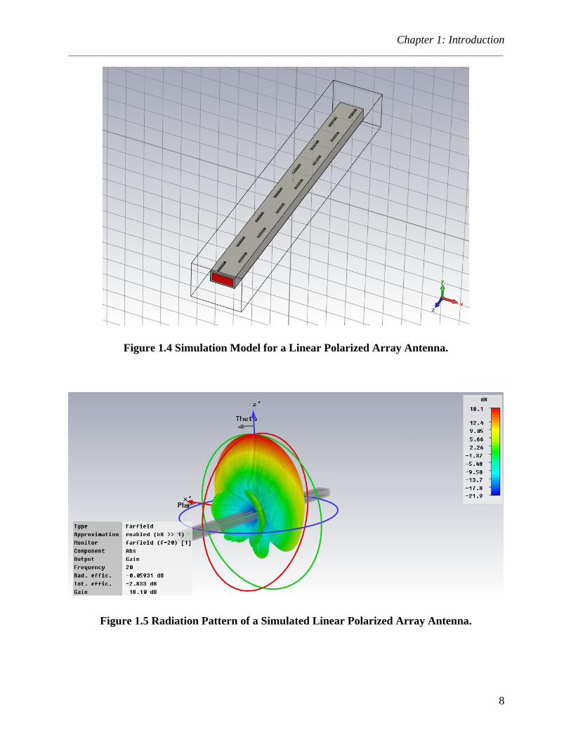
Figure 1.4 represents a design of a linear polarized antenna with elements placed on
opposite side to the center line with an inter-element spacing of a half-guide wavelength. The
slot elements are placed half-guide wavelength apart and are offset on the opposite side of the
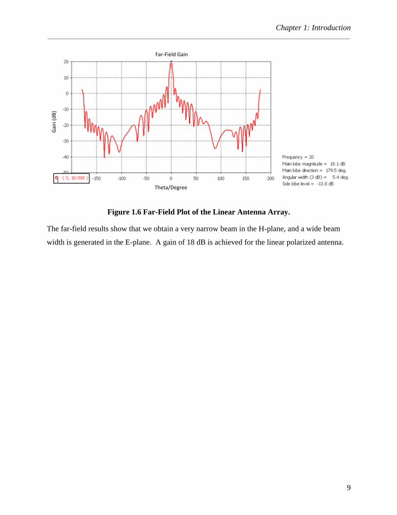
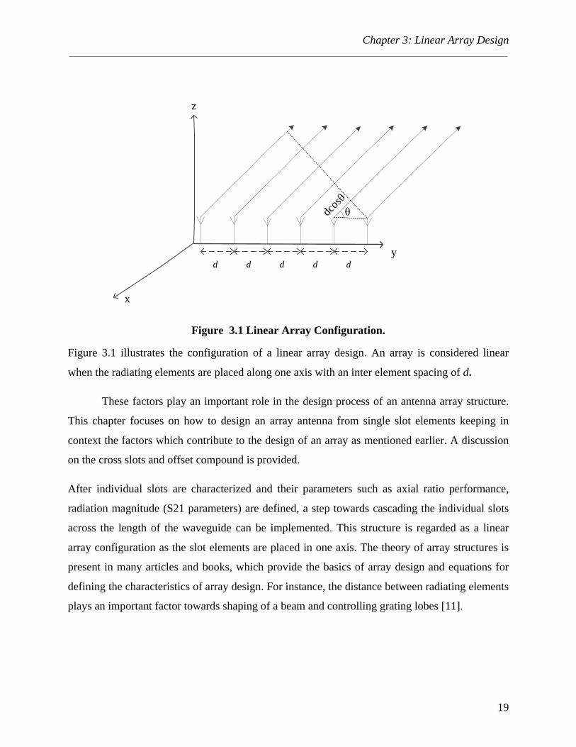
center line so as to cancel out the guide phase advance. Figure 1.5 and Figure 1.6 show the
radiation pattern of a linear polarized antenna, respectively. Following the guidelines developed
in earlier studies, linear polarized antenna can be designed quite efficiently.
Chapter 1: Introduction
8
Figure 1.4 Simulation Model for a Linear Polarized Array Antenna.
Figure 1.5 Radiation Pattern of a Simulated Linear Polarized Array Antenna.
Chapter 1: Introduction
9
Far-Field GainG
ain
(d
B)
Theta/Degree
Figure 1.6 Far-Field Plot of the Linear Antenna Array.
The far-field results show that we obtain a very narrow beam in the H-plane, and a wide beam
width is generated in the E-plane. A gain of 18 dB is achieved for the linear polarized antenna.

Chapter 2: Design of Circular Polarized Antenna Structures
10
Chapter 2
Design of Circular Polarized Antenna
Structures
Having reviewed some theory behind slotted waveguide antennas in Chapter 1, this
section discusses about the design of circular polarized slotted waveguide structures which are
the main focus of this study. Individual radiating elements are investigated which are capable of
generating a circular polarized beam before proceeding towards the design of a linear array
which is presented in Chapter 3.
2.1 Circular Polarized Slots
The study on achieving circular polarized slotted waveguides dates back half a century,
when Watson [22] came up with a proposition that orthogonal slots placed at a specific distance
from the center line produce a circularly polarized wave. A further study was performed by Alan
J. Simmons [6], he carried on the work of Watson and gave an experimental study of cross slot
radiators. Simmons [6] in his research discovered that if a slot is displaced from the center line
by a distance which is defined by (4), then the cross slot will generate a pure circular polarized
wave:
(√(
) ) (4)
where a is the inner dimension of broad side wall of the waveguide. is the free space
wavelength. is the displacement of the slot from center line. is the inverse of cotangent.
A further study was performed by J. Hirokawa [7]. His research is based on arrays based on
cross slot and antenna structures were designed to be used for satellite communications.

Chapter 2: Design of Circular Polarized Antenna Structures
11
Figure 2.1 From top to Bottom: Circular Polarized Elements T-slot, X-slot and Offset
Compound Slot.

Chapter 2: Design of Circular Polarized Antenna Structures
12
Figure 2.1 presents different slot structures which can be used for generating a circular
polarization. These structures are known as
T-Slot Structure.
Cross Slot Structure.
Offset Compound Slot Structure.
2.2 Single Slot Characterization
The procedure for characterization of the slot is to design a single slot structure and then
evaluate the parameters of the antenna. Slot characterization was performed for both cross slots
and offset compound slot structures. T-slots were not considered in this study as both cross and
offset compound slot are suggested to have a better axial ratio performance than T-slots. The
parameters that need to be evaluated are:
1) Axial ratio,
2) Reflection, S-parameter ,
3) Slot angles,
4) Spacing for compound slot structures.
Single slot characterization of slots was performed on a small section of a Waveguide
Rectangular (WR)-34 waveguide. The waveguide section is filled with Teflon having a dielectric
of =2.1. The reason for loading the waveguide with Teflon is discussed in Section 3.1.2. The
following section is focused on the study of cross and compound slots.

Chapter 2: Design of Circular Polarized Antenna Structures
13
2.3 X-Slots
As mentioned briefly earlier in the chapter, the cross slots are capable of generating a
circular polarized wave with a good axial ratio performance. The slots are oriented so as to form
an orthogonal pair of slots which eventually generate a circular polarized wave. The slot can be
characterized by using a model developed in Computer Simulation Technology (CST)
Microwave Studio or High Frequency Structural Simulator (HFSS).
From (4), we can determine the point in the broad wall of the waveguide at which the slots are
capable of generating a pure circular polarization. The theory of cross slots also suggests that the
slots should be ideally equal to half of the free space wavelength. At this length, they exhibit
resonance at the designed frequency. In order to fit in this slot size, the cross slot structure has to
be rotated by 45 degrees. The structure based on cross slot design is shown in Figure 2.2.
Figure 2.2 Cross Slot Configuration.

Chapter 2: Design of Circular Polarized Antenna Structures
14
Axia
l R
atio
(dB
)
Far-Field Axial Ratio
Theta/Degree
Figure 2.3 Axial Ratio for Cross Slot.
For the simulation setup, there are two ports assigned for the model, one for input and the
other one assigned at the end of the waveguide structure. It is observed that when placing a X-
slot at a distance specified by Simmons equation, and taking the inner dimension of the
waveguide as 8.66 mm, we get a position for the slot offset which defines a good value of axial
ratio performance as seen in Figure 2.3. The value of offset comes out to be 3.3 mm, but at this
point the slot length of half free space wavelength cannot be accommodated in the waveguide
broad wall and so an adjustment needs to be made.
An analysis of the E-field distribution for different slot lengths was also performed as it
provides information about the amount of energy coupled in the free space by the element for
each individual length of the slot element.

Chapter 2: Design of Circular Polarized Antenna Structures
15
Measuring Line Length (mm)
E F
ield
Str
eng
th (
V/m
)Slot Length(mm)
Figure 2.4 Magnitude of E-field radiated.
Figure 2.4 shows the magnitude of the E-field with varying slot lengths. The other way
could be to observe the scattering parameter , which gives an idea about the magnitude of
power received at the other port which is at the termination of the waveguide. The far-field
characteristics show that a Left Handed Circularly Polarized (LHCP) wave is produced by this
kind of structure slot configuration and can be changed to Right Handed Circularly Polarized
(RHCP) by feeding the structure from the opposite end.
2.4 Offset Compound Slot Pair
The offset compound slot pair is a relatively new approach for generating a circular
polarized wave. Earlier studies on a slot structure offset from the center line of the broadside of
the waveguide structure were studied by Maxum [8]. Later, Rengarajan [9] made some
interesting analysis of a broad wall radiating slot, which is offset from the center line and tilted
by an angle with reference to the longitudinal axis of the rectangular waveguide. Rengarajan
performed a detailed mathematical calculation of the fields created inside the waveguide due to
the slot structure, which he named as compound slot.

Chapter 2: Design of Circular Polarized Antenna Structures
16
Recently, a new design approach was adapted by Giorgio Montisci [10], which combines
a compound slot structure in a formation which generates a good circular polarized wave with
good axial ratio performance. A couple of papers have been published by the author [13] [14] on
this topic which realizes a numerically efficient method of moments (MoM) analysis of the offset
compound slot structure. The design is said to be simulated for 7.5 GHz.
In this study, a comprehensive design approach has been outlined which defines how the
single elements were designed and what parameters are to be considered in the design approach.
The two interacting inclined radiating slots are cut in the broad wall of a waveguide. Each slot
element is placed at a distance and with an angle theta. These parameters along with the length of
the slots can be used as design parameters in order to obtain the required polarization and
amplitude of the radiating field.
To proceed for the design of a single element, it is completely possible to select some arbitrary
values of tilt angle, offset and width of the slots. The parameter for the spacing of the slots, then,
can be utilized to define the axial ratio value of the slots. Figure 2.5 shows the offset compound
slot structure. The slots are placed almost orthogonal to each other.
Figure 2.5 Compound Slot Configuration.

Chapter 2: Design of Circular Polarized Antenna Structures
17
The axial ratio performance of the slot is comparable to that of cross slots and seems to
be a good choice of slot configuration. The axial ratio can be optimized by running a parameter
sweep on the spacing between the orthogonal slot structures and observing the axial ratio value.
From the S21 curve in Figure 2.6, we can observe the magnitude of the power received at the
terminating end for variable slot lengths. From this curve, we can choose the amplitude of the
radiating field by changing the slot length. The spacing for the highest axial ratio performance
was chosen which comes out to be 3 mm, and offset for the element was varied so fit in the
desired slot length. The offset was varied from 1.8 to 2.1 mm. The slot offset from center line is
discussed in Chapter 3 and values can be observed in Table 3-5.
Figure 2.6 S21 Parameters for varying length of compound slot at 20 GHz.
5.2 5.3 5.4 5.5 5.6 5.7 5.8 5.9 6 6.1 6.2 6.3 6.4 6.5 6.60.5
0.6
0.7
0.8
0.9
1
Slot length (mm)
Magnitude (
Lin
ear)
S21 Parameter

Chapter 3: Linear Array Design
18
Chapter 3
Linear Array Design
As is the case with other conventional antennas and as observed earlier, a single slot antenna
structure produces a wide radiation pattern and provides a relatively low value of directivity. As
a major requirement for long range communications, antennas are to be designed such that they
produce a very directive beam pattern. This can be achieved by having a large electrical size of
the antenna. Alternatively, this can be practically achieved by placing the designed single
radiating element in a geometrical configuration which is referred to as an array. According to
[11], in an array antenna there are five parameters which effect the shape of the overall antenna
pattern, these are as follows:
1) The geometrical configuration of the array.
2) The relative displacement between the elements.
3) The excitation amplitude of the elements.
4) The excitation phase.
5) The relative pattern of the elements.
Chapter 3: Linear Array Design
19
d d d d d
θ
dc
osθ
z
x
y
Figure 3.1 Linear Array Configuration.
Figure 3.1 illustrates the configuration of a linear array design. An array is considered linear
when the radiating elements are placed along one axis with an inter element spacing of d.
These factors play an important role in the design process of an antenna array structure.
This chapter focuses on how to design an array antenna from single slot elements keeping in
context the factors which contribute to the design of an array as mentioned earlier. A discussion
on the cross slots and offset compound is provided.
After individual slots are characterized and their parameters such as axial ratio performance,
radiation magnitude (S21 parameters) are defined, a step towards cascading the individual slots
across the length of the waveguide can be implemented. This structure is regarded as a linear
array configuration as the slot elements are placed in one axis. The theory of array structures is
present in many articles and books, which provide the basics of array design and equations for
defining the characteristics of array design. For instance, the distance between radiating elements
plays an important factor towards shaping of a beam and controlling grating lobes [11].

Chapter 3: Linear Array Design
20
3.1 Design Procedure
The single slot structures are designed in view of the axial ratio performance they exhibit and
amount of energy they couple to the free space. The slot structures are then supposed to be
cascaded along the length of the waveguide. This demands some detailed analysis regarding the
placement of the slots. There are a few problems that need to be addressed before proceeding
with the linear array design.
3.1.1 Grating lobe problem
While designing linear slot arrays, it is to be observed that resonant array design requires in-
phase elements to be placed at half-guide wavelength apart and to cancel the guide phase
advance, alternating slots are placed on the opposite side of the center line in case of longitudinal
slots, or the rotation angle is reversed for edge slots [3], as seen Figure 1.3 where a structure of
linear polarized antenna is shown. This kind of technique is not possible with circular slot
structures. Therefore, the slot, when placed at a distance of guide wavelength apart, produces
grating lobes in addition to the main lobe. These lobes are highly undesirable and tend to reduce
the aperture efficiency. Moreover, as the array antenna is to be used for satellite
communications, it is highly undesirable to have the grating lobes as they cause interference with
other sources. The requirement for not having grating lobes is discussed in [11]. To avoid any
grating lobes, the largest spacing between the elements should be less than one wavelength:
(5)
where is the maximum distance between the radiating elements. For space
communications, a standard needs to be followed also for side lobe levels [15], which will be
discussed in Chapter 5 for array design.
The wavelength inside a waveguide is computed as
√ (
) ( )
where is the free space wavelength computed by =c/f , replacing c with speed of light and f
with frequency 20 GHz, we find to be 15 mm.

Chapter 3: Linear Array Design
21
defines the cutoff inside the waveguide and is found to be . Substituting a=8.66 mm,
we obtain = 17.32 mm. Replacing these values in (6), the guide wavelength can be found as
√ (
) ( )
Therefore, the guide wavelength is greater than the free space wavelength, if the
waveguide is filled with air inside. Placing elements at a guide wavelength will produce grating
lobes. Figure 3.2 shows the existence of grating lobes.
Figure 3.2 Radiation Pattern with Grating Lobes.

Chapter 3: Linear Array Design
22
Proposed solution for grating lobes issue
The main idea to get this issue of grating lobes resolved is to generate a slow wave inside
the waveguide. In other words, the guide wavelength should be made less than the free space
wavelength . The solution to this problem is discussed in earlier design methods such as the
one by A. J. Sangster [12] in which he proposes a corrugated waveguide structure, which creates
a guide wavelength less than the free space frequency. In our case, the frequency of operation
of 20 GHz translates to a free space wavelength of 15mm.
Although the corrugated structure fulfills the requirement of generating a slow wave
inside the waveguide, it has its drawbacks in terms of complexity for defining the actual guide
wavelength value propagating inside the wave guide structure. Moreover, it requires precise
machining. At 20 GHz the dimensions of the structure are already quite small, which can cause
more complexity when fabricating the antenna structure.
Another solution to this problem is to fill the inner space of waveguides with a dielectric
material. This would significantly reduce the guide wavelength less than the free space
wavelength. The waveguide was filled with Teflon having a relative permittivity of = 2.1.
It is know that the relationship between wavelength and dielectric is given by
√ ( )
For = 2.1 and we get λ = 10.35 mm. Putting this new value of in (7), we get
the value of guide wavelength inside the waveguide. From
√ (
)
(9)
we obtain

Chapter 3: Linear Array Design
23
√ (
) ( )
which is less than the free space wavelength of 15 mm. If we now design a linear array by
placing individual elements a guide wavelength apart, the grating lobe problem will be resolved.
This method provides a quick solution and is ideal in building an initial prototype and
performing simulations. Further study can be conducted to identify more structures which have
fewer drawbacks. For instance, while using a dielectric filled waveguide, the antenna efficiency
is reduced, especially, when used in large array structures.
3.1.2 Dimensions of Waveguide
As we have adapted an approach to use a dielectric filled waveguide in our design,
another parameter needs to be considered which is choosing the appropriate dimensions of the
waveguide. A common choice would be to use a standard waveguide, which in this case will be
WR 42. It can be used in the frequency range of 18.00 - 26.50 GHz, and has dimensions of a =
12.7 mm and b = 6.35 mm. If we use this waveguide for our design frequency of 20 GHz, this
will not be a good approach. The reason behind this is that as the waveguide has been loaded
with a dielectric material, the cut off frequency of the first order mode in the waveguide is not
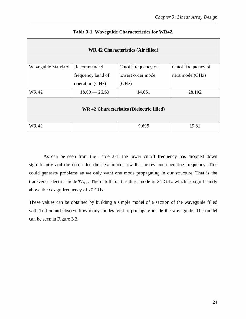
the same as defined in the datasheet of the waveguide. The values can be seen in Table 3-1.
Chapter 3: Linear Array Design
24
Table 3-1 Waveguide Characteristics for WR42.
WR 42 Characteristics (Air filled)
Waveguide Standard Recommended
frequency band of
operation (GHz)
Cutoff frequency of
lowest order mode
(GHz)
Cutoff frequency of
next mode (GHz)
WR 42 18.00 — 26.50 14.051 28.102
WR 42 Characteristics (Dielectric filled)
WR 42 9.695 19.31
As can be seen from the Table 3-1, the lower cutoff frequency has dropped down
significantly and the cutoff for the next mode now lies below our operating frequency. This
could generate problems as we only want one mode propagating in our structure. That is the
transverse electric mode . The cutoff for the third mode is 24 GHz which is significantly
above the design frequency of 20 GHz.
These values can be obtained by building a simple model of a section of the waveguide filled
with Teflon and observe how many modes tend to propagate inside the waveguide. The model
can be seen in Figure 3.3.
Chapter 3: Linear Array Design
25
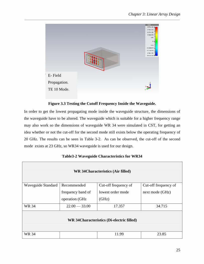
Figure 3.3 Testing the Cutoff Frequency Inside the Waveguide.
In order to get the lowest propagating mode inside the waveguide structure, the dimensions of
the waveguide have to be altered. The waveguide which is suitable for a higher frequency range
may also work so the dimensions of waveguide WR 34 were simulated in CST, for getting an
idea whether or not the cut-off for the second mode still exists below the operating frequency of
20 GHz. The results can be seen in Table 3-2. As can be observed, the cut-off of the second
mode exists at 23 GHz, so WR34 waveguide is used for our design.
Table3-2 Waveguide Characteristics for WR34
WR 34Characteristics (Air filled)
Waveguide Standard Recommended
frequency band of
operation (GHz
Cut-off frequency of
lowest order mode
(GHz)
Cut-off frequency of
next mode (GHz)
WR 34 22.00 — 33.00 17.357 34.715
WR 34Characteristics (Di-electric filled)
WR 34 11.99 23.85
E- Field
Propagation.
TE 10 Mode.
Chapter 3: Linear Array Design
26
3.2 Linear Array Design
Having addressed the issues of grating lobe and selection of right dimensions for the
waveguide structure, we can proceed further towards design of linear array. The linear array
structure was realized in CST for both cross and offset compound slot structure. It is a good
approach to see what advantages and drawbacks both structures exhibit. The following sections
discuss the design procedure and simulation results obtained for both linear antenna arrays.
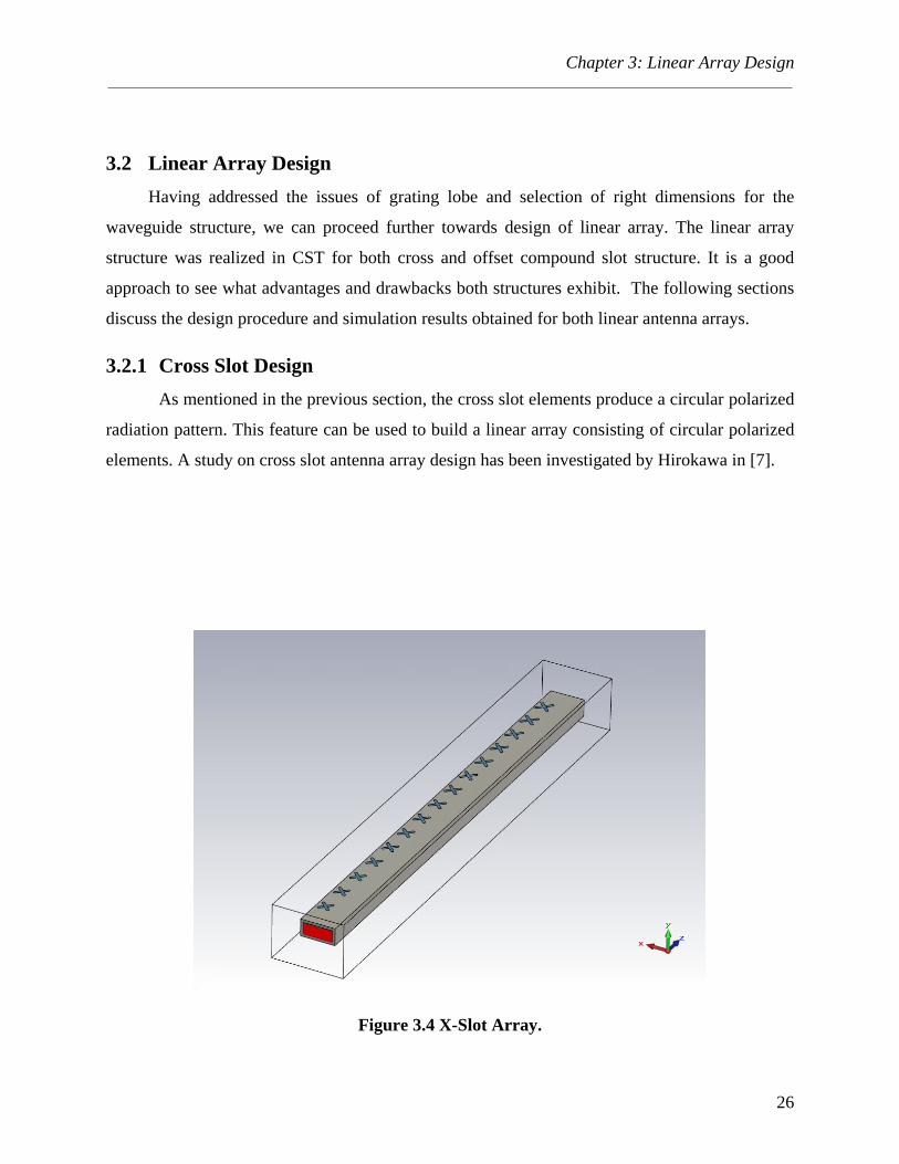
3.2.1 Cross Slot Design
As mentioned in the previous section, the cross slot elements produce a circular polarized
radiation pattern. This feature can be used to build a linear array consisting of circular polarized
elements. A study on cross slot antenna array design has been investigated by Hirokawa in [7].
Figure 3.4 X-Slot Array.
Chapter 3: Linear Array Design
27
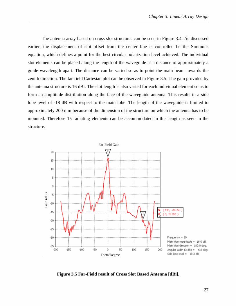
The antenna array based on cross slot structures can be seen in Figure 3.4. As discussed
earlier, the displacement of slot offset from the center line is controlled be the Simmons
equation, which defines a point for the best circular polarization level achieved. The individual
slot elements can be placed along the length of the waveguide at a distance of approximately a
guide wavelength apart. The distance can be varied so as to point the main beam towards the
zenith direction. The far-field Cartesian plot can be observed in Figure 3.5. The gain provided by
the antenna structure is 16 dBi. The slot length is also varied for each individual element so as to
form an amplitude distribution along the face of the waveguide antenna. This results in a side
lobe level of -18 dB with respect to the main lobe. The length of the waveguide is limited to
approximately 200 mm because of the dimension of the structure on which the antenna has to be
mounted. Therefore 15 radiating elements can be accommodated in this length as seen in the
structure.
Theta/Degree
Gai
n (
dB
i)
Far-Field Gain
Figure 3.5 Far-Field result of Cross Slot Based Antenna [dBi].

Chapter 3: Linear Array Design
28
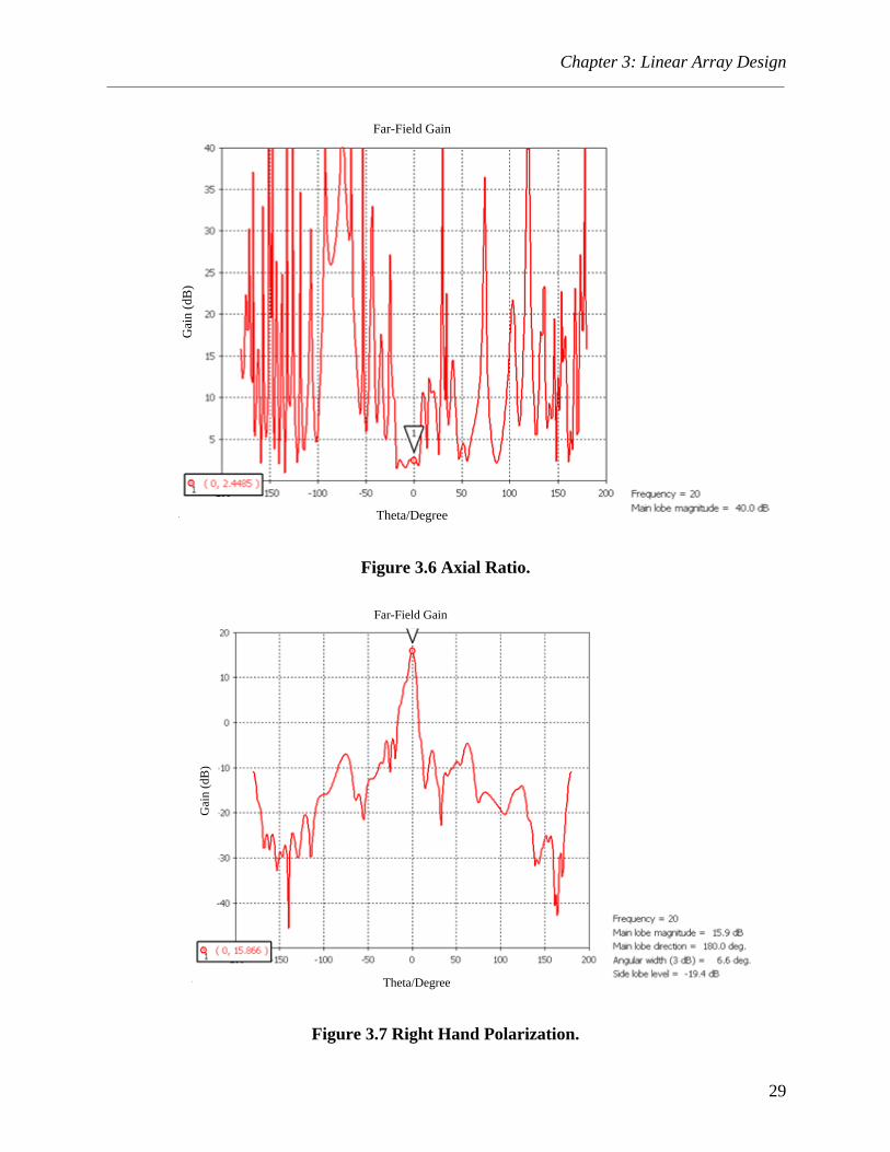
After getting the main beam to be fixed in the zenith direction, a parametric sweep can be
performed on the displacement factor from the center line of the waveguide antenna to find out
the best axial ratio performance. Figure 3.6 shows the axial ratio performance of the antenna
structure. Although the axial ratio performance observed for the individual cross slot element
was quite good, the overall axial ratio performance of the linear antenna array is observed to be
2.4 dB.
As can be observed in Figure 3.6 the axial ratio is better around zero degrees and tends to
degrade as we move further away from the zenith direction. Figure 3.7 and Figure 3.8 represent
the difference between left and right polarization. The polarization purity is quite good and the
difference between left and right polarization is around 15 dB.
Chapter 3: Linear Array Design
29
Gai
n (
dB
)
Far-Field Gain
Theta/Degree
Figure 3.6 Axial Ratio.
Gai
n (
dB
)
Far-Field Gain
Theta/Degree
Figure 3.7 Right Hand Polarization.
Chapter 3: Linear Array Design
30
Gai
n (
dB
)
Far-Field Gain
Theta/Degree
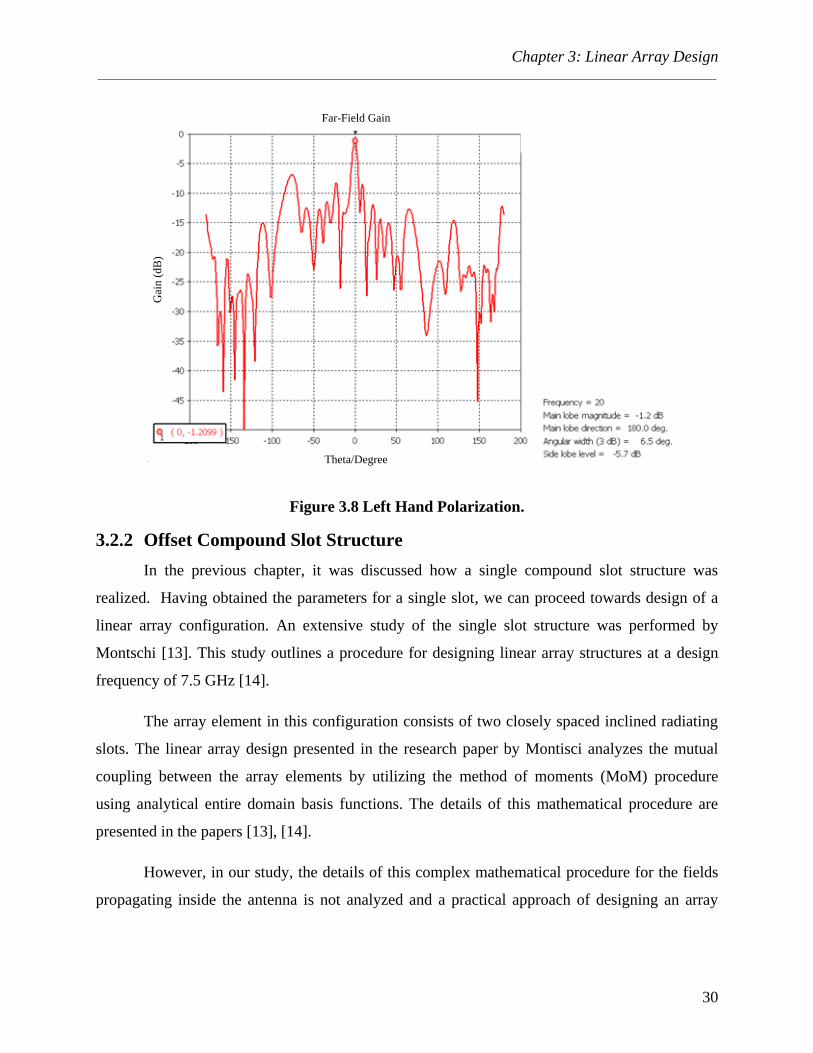
Figure 3.8 Left Hand Polarization.
3.2.2 Offset Compound Slot Structure
In the previous chapter, it was discussed how a single compound slot structure was
realized. Having obtained the parameters for a single slot, we can proceed towards design of a
linear array configuration. An extensive study of the single slot structure was performed by
Montschi [13]. This study outlines a procedure for designing linear array structures at a design
frequency of 7.5 GHz [14].
The array element in this configuration consists of two closely spaced inclined radiating
slots. The linear array design presented in the research paper by Montisci analyzes the mutual
coupling between the array elements by utilizing the method of moments (MoM) procedure
using analytical entire domain basis functions. The details of this mathematical procedure are
presented in the papers [13], [14].
However, in our study, the details of this complex mathematical procedure for the fields
propagating inside the antenna is not analyzed and a practical approach of designing an array
Chapter 3: Linear Array Design
31
structure is adopted rather than going into the complex mathematical analysis of mutual coupling
effects and other parameters.
The design achieved shows good results both in simulation and implementation, as
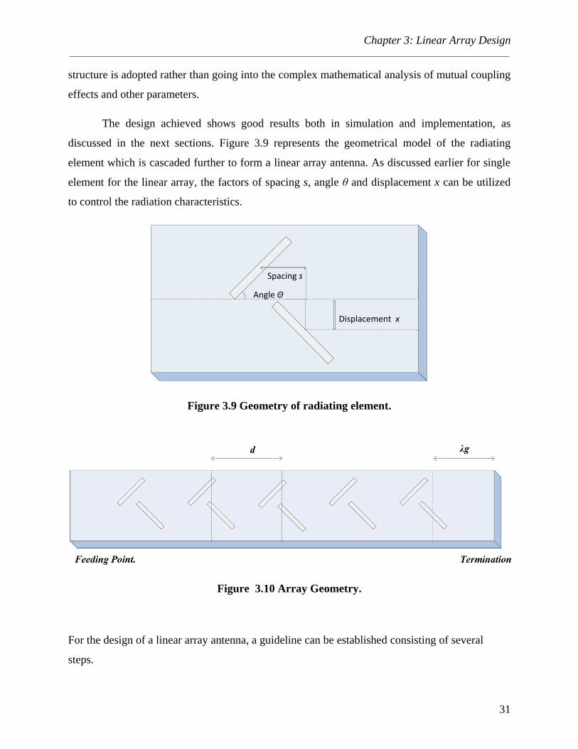
discussed in the next sections. Figure 3.9 represents the geometrical model of the radiating
element which is cascaded further to form a linear array antenna. As discussed earlier for single
element for the linear array, the factors of spacing s, angle θ and displacement x can be utilized
to control the radiation characteristics.
Displacement x
Spacing s
Angle Θ
Figure 3.9 Geometry of radiating element.
Figure 3.10 Array Geometry.
For the design of a linear array antenna, a guideline can be established consisting of several
steps.
Chapter 3: Linear Array Design
32
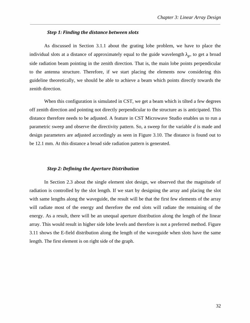
Step 1: Finding the distance between slots
As discussed in Section 3.1.1 about the grating lobe problem, we have to place the
individual slots at a distance of approximately equal to the guide wavelength , to get a broad
side radiation beam pointing in the zenith direction. That is, the main lobe points perpendicular
to the antenna structure. Therefore, if we start placing the elements now considering this
guideline theoretically, we should be able to achieve a beam which points directly towards the
zenith direction.
When this configuration is simulated in CST, we get a beam which is tilted a few degrees
off zenith direction and pointing not directly perpendicular to the structure as is anticipated. This
distance therefore needs to be adjusted. A feature in CST Microwave Studio enables us to run a
parametric sweep and observe the directivity pattern. So, a sweep for the variable d is made and
design parameters are adjusted accordingly as seen in Figure 3.10. The distance is found out to
be 12.1 mm. At this distance a broad side radiation pattern is generated.
Step 2: Defining the Aperture Distribution
In Section 2.3 about the single element slot design, we observed that the magnitude of
radiation is controlled by the slot length. If we start by designing the array and placing the slot
with same lengths along the waveguide, the result will be that the first few elements of the array
will radiate most of the energy and therefore the end slots will radiate the remaining of the
energy. As a result, there will be an unequal aperture distribution along the length of the linear
array. This would result in higher side lobe levels and therefore is not a preferred method. Figure
3.11 shows the E-field distribution along the length of the waveguide when slots have the same
length. The first element is on right side of the graph.

Chapter 3: Linear Array Design
33
Measuring Line Length (mm)
E-F
ield
Str
eng
th (
V/m
)
Figure 3.11 Amplitude Distribution with Same Slot Length.
An aperture distribution (Taylor or Chebyshev) will help to minimize the side lobe levels
of the antenna. A distribution can be realized theoretically by having a look at the curve which
shows the S21 parameter of the single radiating slot. This result can be used to calculate the
radiated power associated with the first element and how the proceeding elements should be
designed to form an aperture distribution along the face of antenna structure.
Different aperture distributions can be used depending on the side lobe level to be
achieved. Table 3-3 shows a brief comparison of the techniques used.
Table 3-3 Comparison of Amplitude Distribution.
Comparison of Amplitude Distribution
Smallest Biggest
Beam Width Uniform Amplitude Dolph-
Tschebycheff/Taylor
Binomial
Side Lobe Level Binomial Dolph-
Tschebycheff/Taylor
Uniform Amplitude.

Chapter 3: Linear Array Design
34
As can be seen from Table 3-3, if the array is fed by uniform amplitude, the side lobe
levels are maximum in this case. A need exists therefore to get the side lobes to a minimum level
to avoid interference with other satellites. Details on the satellite system standards can be found
in the article for satellite communications standards [15]. The coefficient of amplitude
distributions can be easily realized in Matlab by using the built in commands of:
Taylorwin.
Chebywin.
The coefficients computed are listed in the Table 3-4 for a 15 element linear array design. It can
be observed from Figure 3-12 and Figure 3-13, the Taylor and Chebyshev distributions based
designs have difference of the main lobe.
Table 3-4 Coefficients of Distributions.
Taylor Distribution Coefficients Chebyshev Distribution Coefficients
0.6575 0.8238
0.5988 0.5116
0.6142 0.6364
0.7333 0.7536
0.8531 0.8550
0.9238 0.9335
0.9750 0.9830
1.0000 1.0000
0.9750 0.9830
0.9238 0.9335
0.8531 0.8550
0.7333 0.7536
0.6142 0.6364
0.5988 0.5116
0.6575 0.8238

Chapter 3: Linear Array Design
35
Figure 3.12 Taylor Distribution.
Figure 3.13 Chebychev Distribution.
2 4 6 8 10 12 140.7
0.8
0.9
1
1.1
1.2
1.3
1.4
Samples
Am
plit
ude
Time domain
-1 -0.5 0 0.5-50
-40
-30
-20
-10
0
10
20
30
Normalized Frequency ( rad/sample)M
agnitude (
dB
)
Frequency domain
2 4 6 8 10 12 140
0.2
0.4
0.6
0.8
1
Samples
Am
plitu
de
Time domain
-1 -0.5 0 0.5-40
-30
-20
-10
0
10
20
30
Normalized Frequency ( rad/sample)
Magnitude (
dB
)
Frequency domain
(lin
ear)
(l
inea
r)
Chapter 3: Linear Array Design
36
While simulating linear arrays, another practical approach can be to observe the
amplitude distribution of the E-field across the face of the linear antenna structure. This can be
done by placing a line across the face of the waveguide and then monitor the E-field along the
curve by using post processing template in CST Studio.
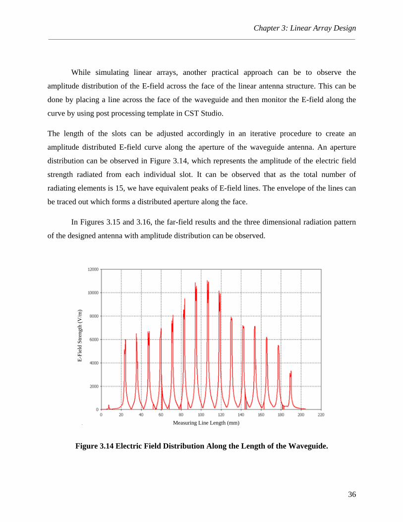
The length of the slots can be adjusted accordingly in an iterative procedure to create an
amplitude distributed E-field curve along the aperture of the waveguide antenna. An aperture
distribution can be observed in Figure 3.14, which represents the amplitude of the electric field
strength radiated from each individual slot. It can be observed that as the total number of
radiating elements is 15, we have equivalent peaks of E-field lines. The envelope of the lines can
be traced out which forms a distributed aperture along the face.
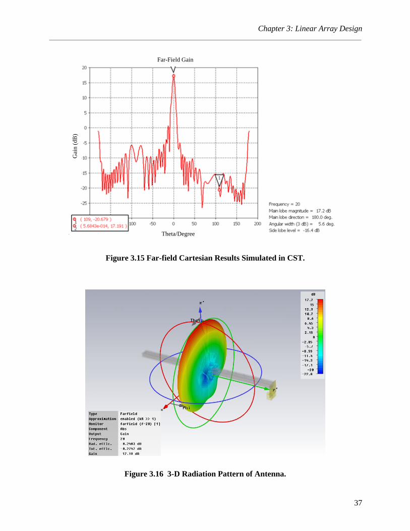
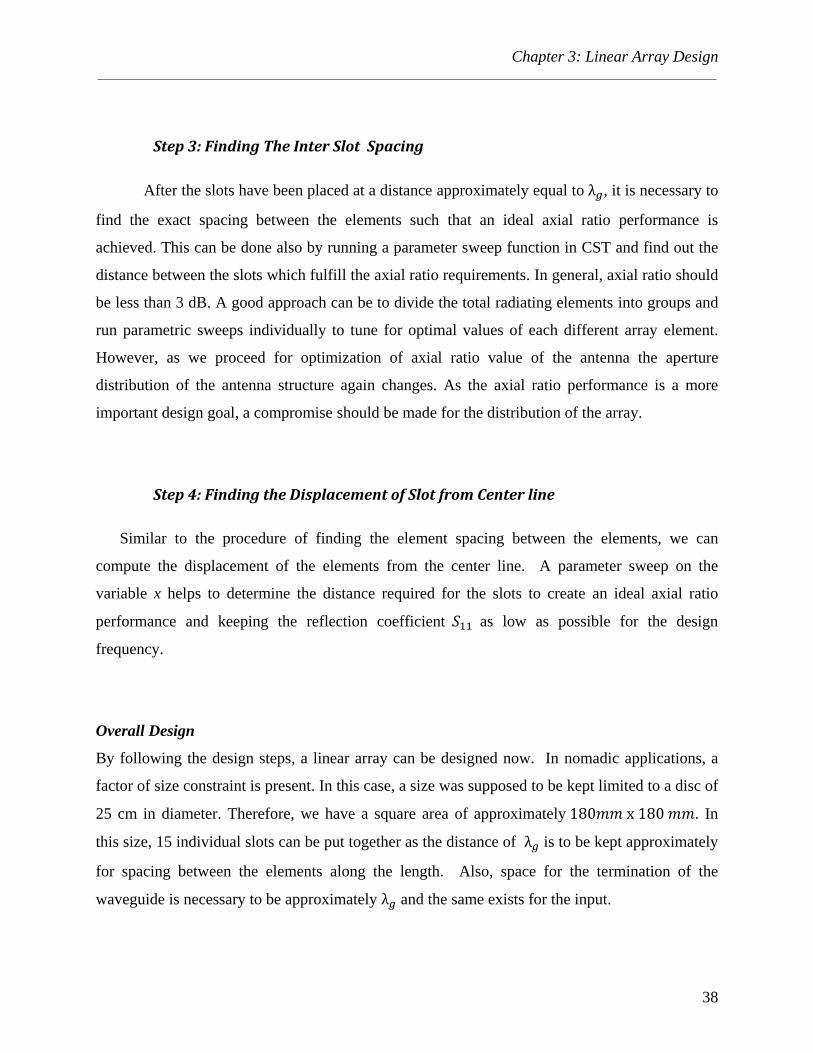
In Figures 3.15 and 3.16, the far-field results and the three dimensional radiation pattern
of the designed antenna with amplitude distribution can be observed.
Measuring Line Length (mm)
E-F
ield
Str
eng
th (
V/m
)
Figure 3.14 Electric Field Distribution Along the Length of the Waveguide.
Chapter 3: Linear Array Design
37
Gai
n (
dB
)
Far-Field Gain
Theta/Degree
Figure 3.15 Far-field Cartesian Results Simulated in CST.
Figure 3.16 3-D Radiation Pattern of Antenna.
Chapter 3: Linear Array Design
38
Step 3: Finding The Inter Slot Spacing
After the slots have been placed at a distance approximately equal to , it is necessary to
find the exact spacing between the elements such that an ideal axial ratio performance is
achieved. This can be done also by running a parameter sweep function in CST and find out the
distance between the slots which fulfill the axial ratio requirements. In general, axial ratio should
be less than 3 dB. A good approach can be to divide the total radiating elements into groups and
run parametric sweeps individually to tune for optimal values of each different array element.
However, as we proceed for optimization of axial ratio value of the antenna the aperture
distribution of the antenna structure again changes. As the axial ratio performance is a more
important design goal, a compromise should be made for the distribution of the array.
Step 4: Finding the Displacement of Slot from Center line
Similar to the procedure of finding the element spacing between the elements, we can
compute the displacement of the elements from the center line. A parameter sweep on the
variable x helps to determine the distance required for the slots to create an ideal axial ratio
performance and keeping the reflection coefficient as low as possible for the design
frequency.
Overall Design
By following the design steps, a linear array can be designed now. In nomadic applications, a
factor of size constraint is present. In this case, a size was supposed to be kept limited to a disc of
25 cm in diameter. Therefore, we have a square area of approximately . In
this size, 15 individual slots can be put together as the distance of is to be kept approximately
for spacing between the elements along the length. Also, space for the termination of the
waveguide is necessary to be approximately and the same exists for the input.
Chapter 3: Linear Array Design
39
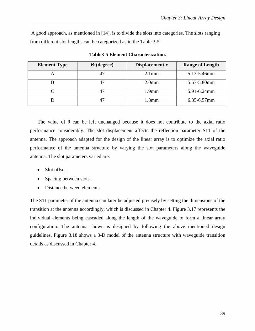
A good approach, as mentioned in [14], is to divide the slots into categories. The slots ranging
from different slot lengths can be categorized as in the Table 3-5.
Table3-5 Element Characterization.
Element Type Θ (degree) Displacement x Range of Length
A 47 2.1mm 5.13-5.46mm
B 47 2.0mm 5.57-5.80mm
C 47 1.9mm 5.91-6.24mm
D 47 1.8mm 6.35-6.57mm
The value of θ can be left unchanged because it does not contribute to the axial ratio
performance considerably. The slot displacement affects the reflection parameter S11 of the
antenna. The approach adapted for the design of the linear array is to optimize the axial ratio
performance of the antenna structure by varying the slot parameters along the waveguide
antenna. The slot parameters varied are:
Slot offset.
Spacing between slots.
Distance between elements.
The S11 parameter of the antenna can later be adjusted precisely by setting the dimensions of the
transition at the antenna accordingly, which is discussed in Chapter 4. Figure 3.17 represents the
individual elements being cascaded along the length of the waveguide to form a linear array
configuration. The antenna shown is designed by following the above mentioned design
guidelines. Figure 3.18 shows a 3-D model of the antenna structure with waveguide transition
details as discussed in Chapter 4.

Chapter 3: Linear Array Design
40
Figure 3.17 Top View of Antenna Model.
mm

Chapter 3: Linear Array Design
41
Figure 3.18 3D view of Linear Array.
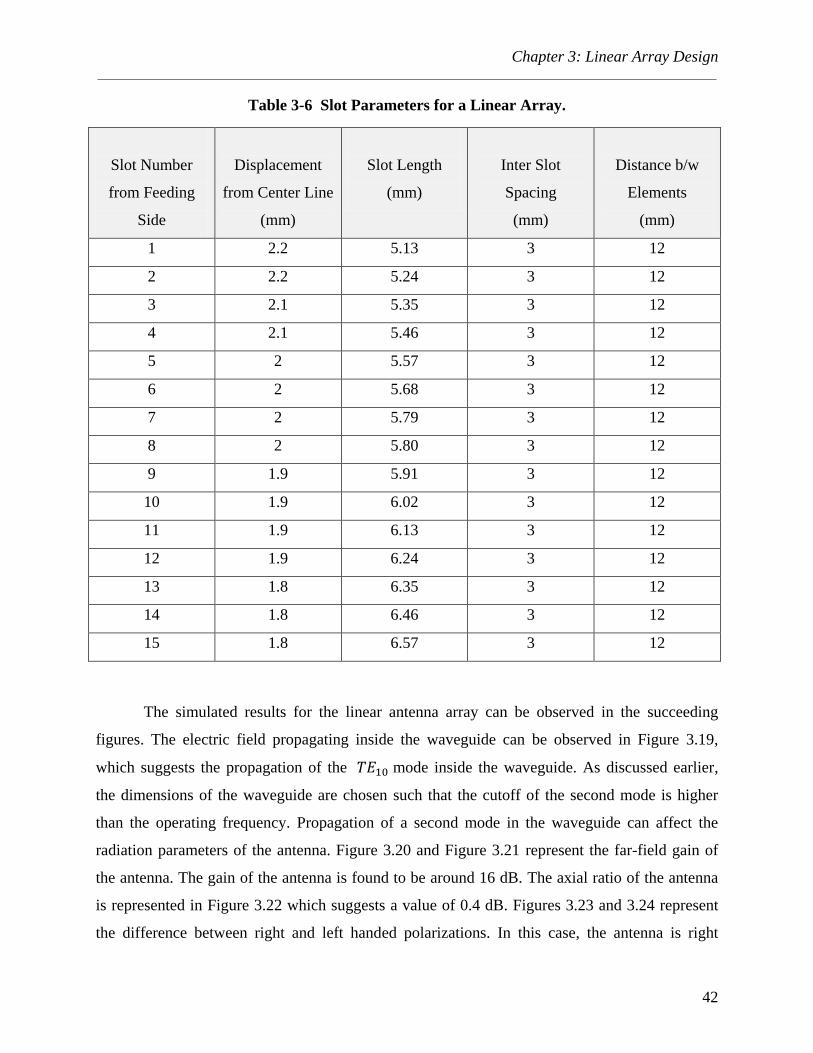
In Table 3-6, the designed array parameters can be observed, the total number of slots in the
array are fifteen each having a different length for aperture distribution.
Chapter 3: Linear Array Design
42
Table 3-6 Slot Parameters for a Linear Array.
Slot Number
from Feeding
Side
Displacement
from Center Line
(mm)
Slot Length
(mm)
Inter Slot
Spacing
(mm)
Distance b/w
Elements
(mm)
1 2.2 5.13 3 12
2 2.2 5.24 3 12
3 2.1 5.35 3 12
4 2.1 5.46 3 12
5 2 5.57 3 12
6 2 5.68 3 12
7 2 5.79 3 12
8 2 5.80 3 12
9 1.9 5.91 3 12
10 1.9 6.02 3 12
11 1.9 6.13 3 12
12 1.9 6.24 3 12
13 1.8 6.35 3 12
14 1.8 6.46 3 12
15 1.8 6.57 3 12
The simulated results for the linear antenna array can be observed in the succeeding
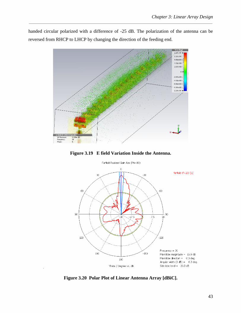
figures. The electric field propagating inside the waveguide can be observed in Figure 3.19,
which suggests the propagation of the mode inside the waveguide. As discussed earlier,
the dimensions of the waveguide are chosen such that the cutoff of the second mode is higher
than the operating frequency. Propagation of a second mode in the waveguide can affect the
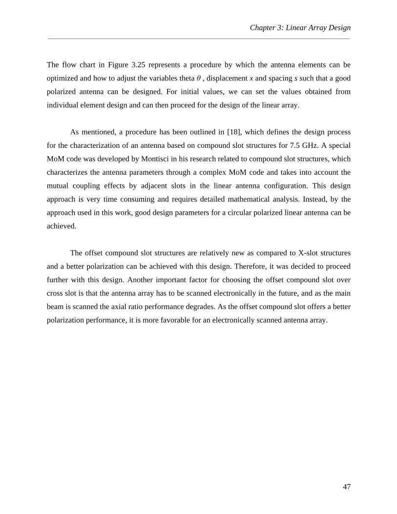
radiation parameters of the antenna. Figure 3.20 and Figure 3.21 represent the far-field gain of
the antenna. The gain of the antenna is found to be around 16 dB. The axial ratio of the antenna
is represented in Figure 3.22 which suggests a value of 0.4 dB. Figures 3.23 and 3.24 represent
the difference between right and left handed polarizations. In this case, the antenna is right
Chapter 3: Linear Array Design
43
handed circular polarized with a difference of -25 dB. The polarization of the antenna can be
reversed from RHCP to LHCP by changing the direction of the feeding end.
Figure 3.19 E field Variation Inside the Antenna.
Figure 3.20 Polar Plot of Linear Antenna Array [dBiC].

Chapter 3: Linear Array Design
44
Figure 3.21 Far-Field Gain of Optimized Antenna [dBiC].
Figure 3.22 Axial Ratio [dB].
Theta/ Degree
Theta/ Degree
Ax
ial
Rat
io (
dB
) G
ain
(d
BiC
)
Far-Field Axial Ratio
Far-Field Gain

Chapter 3: Linear Array Design
45
Figure 3.23 Right Hand Polarization.
Figure 3.24 Left Hand Polarization.
Theta/ Degree
Theta/ Degree
Gai
n (
dB
) G
ain (
dB
)
Far-Field Gain
Far-Field Gain

Chapter 3: Linear Array Design
46
The antenna parameters which can be used to control the radiation characteristics of the
antenna are described in Table 3-7.
Table 3-7 Controlling Antenna Characteristics
Antenna Radiation Parameters
Axial ratio requirement Proper choice of spacing s
Element excitation Varying length of slot
S11 requirement Setting values of tilt angles θ, Slot offsets from center line x
Main beam tilt Control distance between individual elements
Change Spacing s and
Check Axial Ratio
Check S11
Assign initial
parameters
Length l
Theta θ
Disp x
Optimize values of
Theta θ Displacement x
Length l
Output Parameters
Yes
No
Check Beam pointing in
Zenith
Yes
No
Change
distance
between
elements d
Figure 3.25 Flow Chart for Optimizing the Antenna Parameters.
Chapter 3: Linear Array Design
47
The flow chart in Figure 3.25 represents a procedure by which the antenna elements can be
optimized and how to adjust the variables theta θ , displacement x and spacing s such that a good
polarized antenna can be designed. For initial values, we can set the values obtained from
individual element design and can then proceed for the design of the linear array.
As mentioned, a procedure has been outlined in [18], which defines the design process
for the characterization of an antenna based on compound slot structures for 7.5 GHz. A special
MoM code was developed by Montisci in his research related to compound slot structures, which
characterizes the antenna parameters through a complex MoM code and takes into account the
mutual coupling effects by adjacent slots in the linear antenna configuration. This design
approach is very time consuming and requires detailed mathematical analysis. Instead, by the
approach used in this work, good design parameters for a circular polarized linear antenna can be
achieved.
The offset compound slot structures are relatively new as compared to X-slot structures
and a better polarization can be achieved with this design. Therefore, it was decided to proceed
further with this design. Another important factor for choosing the offset compound slot over
cross slot is that the antenna array has to be scanned electronically in the future, and as the main
beam is scanned the axial ratio performance degrades. As the offset compound slot offers a better
polarization performance, it is more favorable for an electronically scanned antenna array.
Chapter 4: Waveguide to Microstrip Transition at 20 GHz
48
Chapter 4
Waveguide to Microstrip Transition at 20
GHz
After the successful design of a circularly polarized linear array element, a need exists to
feed the waveguide antenna in an efficient way. The typical and straightforward solution to this
is the use of a conventional waveguide to co-axial adapter. This is quite an expensive solution
keeping in mind that we have to feed eventually 14 to 16 linear arrays to form a planar array
antenna structure. Although this solution is simple and provides a convenient way of connecting
the waveguide, it has its disadvantages in terms of cost and the integration with the feed network
design. A new design approach therefore should be considered to minimize the transition losses
at the design frequency.

Chapter 4: Waveguide to Microstrip Transition at 20 GHz
49
4.1 Existing Designs
There exist a couple of design solutions for the transition from microstrip to waveguide.
These offer a cheap solution to integrate the waveguide antenna with feed network printed circuit
board [16]. Further study reveals that most designs consist of a microstrip antenna with a
waveguide reflector at a distance of λ/2. This design has some drawbacks in terms of
manufacturing complexity. An area has to be cut out of a waveguide structure on the back side
and filled with a dielectric, as is necessary in our design. Furthermore, joining this structure with
the rest of the antenna is also a difficult task as the waveguide dimensions are quite small at this
frequency range and wall thickness is only 1.02 mm.
An interesting design is mentioned in [16] which utilizes a patch antenna etched on one
side of the printed circuit board and fed by a feeding line running below the antenna as shown in
Figure 4.1.
Figure 4.1 Patch Antenna.

Chapter 4: Waveguide to Microstrip Transition at 20 GHz
50
Although this transition is said to provide good results, the drawback of it is that it
requires a two layer design procedure. This is expensive and also integrating it with the
waveguide is a complex task as on the bottom layer a ground plane cannot be attached directly.
A simpler approach can be adopted by designing the patch antenna transition on a single layer;
this design can be found in [17]. In this approach, the simple patch antenna technique can be
implemented which provides an advantage of manufacturing simplicity while achieving a low
transition loss. A couple of other methods have also been studied and some simulated in CST
Microwave Studio to realize the best possible design, both in terms of performance and
manufacturing.
4.2 Design of Microwave to Waveguide Transition
As discussed earlier, design approaches which require a second signal layer on the back
side of the patch antenna are not a suitable choice for integration with the waveguide antenna.
The solution to this could be to add another ground layer but this would add to the cost of design.
Another approach was simulated in CST Microwave Studio which utilizes a pin transition which
replicates the co axial to waveguide transition approach. There is a stub matching on the back
side of the Printed Circuit Board (PCB) structure. By varying the length of the pin and stub, we
can achieve a transition to the waveguide antenna. The model is shown in Figure 4.2.
Figure 4.2 Pin Fed Wave Guide Transition.

Chapter 4: Waveguide to Microstrip Transition at 20 GHz
51
Figure 4.3 Complete Model of Pin Fed Waveguide Transition.
On the back side of this transition, we have a stub which needs to be filled with a dielectric also.
The complete design can be seen in Figure 4.3.
A simple design approach as reported in [17] is to utilize a patch antenna on one plane
and a ground plane on the other. This seems to be a good approach for the this kind of microstrip
to waveguide transition as the design seems to be simpler and also allows to be mounted on the
face of the waveguide antenna directly without having any other waveguide stub on the back
side. The design can be seen in the Figure 4.4. The patch dimensions have to be adjusted
accordingly to provide an excellent transition at 20 GHz center frequency.

Chapter 4: Waveguide to Microstrip Transition at 20 GHz
52
Figure 4.4 Patch Transition.
The patch antenna designed is then integrated with a waveguide antenna with holes
mounted on the edges of the antenna. The dimensions of the antenna are then to be tuned to get a
good transition from co-planar waveguide to the waveguide antenna structure and also the
reflections S11 are to be minimized at the design frequency. For finding the dimension of length
and width the following equations are used:
√ ( )
√
( )
Chapter 4: Waveguide to Microstrip Transition at 20 GHz
53
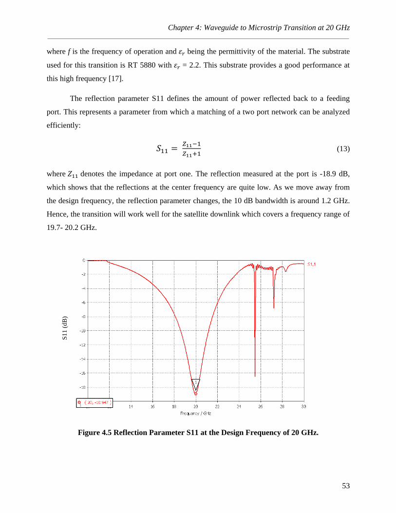
where f is the frequency of operation and being the permittivity of the material. The substrate
used for this transition is RT 5880 with = 2.2. This substrate provides a good performance at
this high frequency [17].
The reflection parameter S11 defines the amount of power reflected back to a feeding
port. This represents a parameter from which a matching of a two port network can be analyzed
efficiently:
(13)
where denotes the impedance at port one. The reflection measured at the port is -18.9 dB,
which shows that the reflections at the center frequency are quite low. As we move away from
the design frequency, the reflection parameter changes, the 10 dB bandwidth is around 1.2 GHz.
Hence, the transition will work well for the satellite downlink which covers a frequency range of
19.7- 20.2 GHz.
Figure 4.5 Reflection Parameter S11 at the Design Frequency of 20 GHz.
S1
1 (
dB
)
Chapter 4: Waveguide to Microstrip Transition at 20 GHz
54
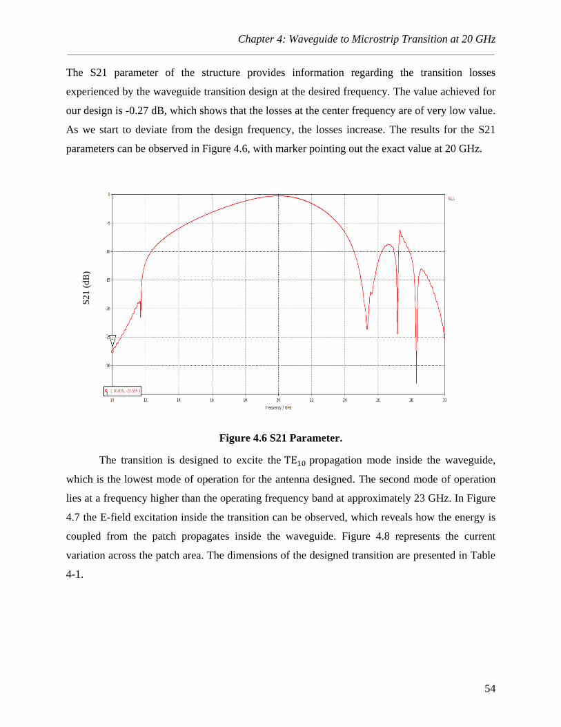
The S21 parameter of the structure provides information regarding the transition losses
experienced by the waveguide transition design at the desired frequency. The value achieved for
our design is -0.27 dB, which shows that the losses at the center frequency are of very low value.
As we start to deviate from the design frequency, the losses increase. The results for the S21
parameters can be observed in Figure 4.6, with marker pointing out the exact value at 20 GHz.
Figure 4.6 S21 Parameter.
The transition is designed to excite the propagation mode inside the waveguide,
which is the lowest mode of operation for the antenna designed. The second mode of operation
lies at a frequency higher than the operating frequency band at approximately 23 GHz. In Figure
4.7 the E-field excitation inside the transition can be observed, which reveals how the energy is
coupled from the patch propagates inside the waveguide. Figure 4.8 represents the current
variation across the patch area. The dimensions of the designed transition are presented in Table
4-1.
S2
1 (
dB
)

Chapter 4: Waveguide to Microstrip Transition at 20 GHz
55
E-Field
Figure 4.7 Electric Field inside Microstrip to Waveguide Transition.
Figure 4.8 E-field Variation on the Surface of the Patch.

Chapter 4: Waveguide to Microstrip Transition at 20 GHz
56
Table 4-1 Waveguide Transition Parameters
Transition Model Dimensions
Dimension of waveguide a(width)=10.66mm, b(height)=6.35,
thickness of walls =1.02mm
Mouse hole dimensions Width =2mm , Height =1 mm
Substrate RT 5880, =2.2
Thickness 0.508 mm
Copper cladding 0.035 mm
Width of CPW feeding the patch 1.1 mm
Patch dimensions Width =7 mm, Length = 3.68mm
Chapter 5: Planar Array Design
57
Chapter 5
Planar Array Design
Previous chapters discuss about designing the linear array for a circularly polarized antenna.
A comprehensive discussion about the planar array theory can be found in ‘‘Antenna Design and
Analysis’’ by C. A. Balanis [11], which discusses about the planar array antenna configurations
and the array factor associated with such type of design. In this chapter, a planar array design is
presented.
Modern antenna arrays are capable of scanning the beam in both elevation and azimuth
planes, but such designs come with the drawback of complex and expensive feed network
design. In this work, an array is implemented which is capable of scanning in one plane
(elevation) by design of feed networks with varying phase and the azimuth scanning is controlled
mechanically. The linear arrays designed in Chapter 3 are placed adjacent to each other so as to
form a planar structure of antennas. All the linear arrays are excited with a microstrip to
waveguide transition designed in the previous section.

Chapter 5: Planar Array Design
58
The configuration of feeding network for the antenna array can be seen in Figure 5.1. The
linear arrays are stacked together and each fed by a phase shifter to form a quasi-planar
configuration. This type of architecture allows scanning the main beam in the elevation plane by
controlling the phase variation of the individual linear arrays. The azimuth scanning can be
achieved by mounting the structure on a mechanical disc.
SOURCE
PHASE SHIFTER
ANTENNAS
Figure 5.1 Array Architecture.
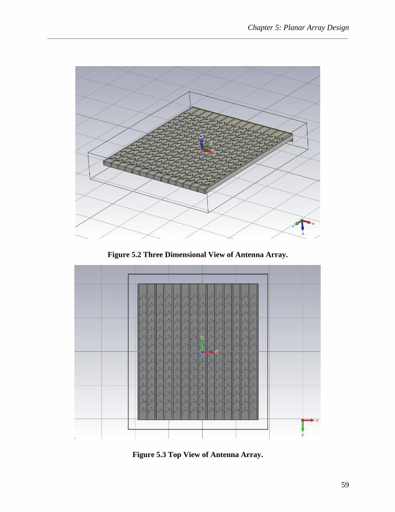
The three dimensional structure and the top view can be seen in Figure 5.2 and Figure 5.3. As
there is a limitation for the size, the number of individual antenna arrays that can be placed
together is limited. Currently, there are 14 linear arrays stacked together. The total area occupied
by the structure is 200 mm x 200mm as observed in Figures 5.2 and 5.3.
Chapter 5: Planar Array Design
59
Figure 5.2 Three Dimensional View of Antenna Array.
Figure 5.3 Top View of Antenna Array.

Chapter 5: Planar Array Design
60
Figure 5.4: Simulated 3-D Pattern of the Array Antenna.
By simulating the whole array structure in CST Microwave Studio, we can observe the
overall radiation characteristics of the array. The gain of the individual linear arrays is combined
together to give a total realized gain of approximately 27.3 dB. The side lobe levels achieved in
this case are at -13 dB. This is because the elements are fed with equal amplitude. The same
technique of applying an aperture distribution to the linear array can be implemented on the
planar array which eventually decreases the side lobe levels. However, this demands for a
sophisticated feed network design which has an amplitude distribution corresponding to different
aperture distributions. Different feeding network topologies can be implemented [19][3]:
Serial Feeding Network.
Parallel /Corporate Feeding Network.
Hybrid Feeding Network.
Chapter 5: Planar Array Design
61
Figure 5.5 Far-Field Cartesian Plot.
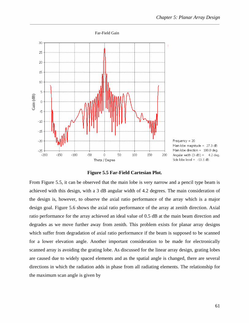
From Figure 5.5, it can be observed that the main lobe is very narrow and a pencil type beam is
achieved with this design, with a 3 dB angular width of 4.2 degrees. The main consideration of
the design is, however, to observe the axial ratio performance of the array which is a major
design goal. Figure 5.6 shows the axial ratio performance of the array at zenith direction. Axial
ratio performance for the array achieved an ideal value of 0.5 dB at the main beam direction and
degrades as we move further away from zenith. This problem exists for planar array designs
which suffer from degradation of axial ratio performance if the beam is supposed to be scanned
for a lower elevation angle. Another important consideration to be made for electronically
scanned array is avoiding the grating lobe. As discussed for the linear array design, grating lobes
are caused due to widely spaced elements and as the spatial angle is changed, there are several
directions in which the radiation adds in phase from all radiating elements. The relationship for
the maximum scan angle is given by
Gai
n (
dB
) Far-Field Gain
Chapter 5: Planar Array Design
62
( )
where d is the inter element spacing and λ is the free space wavelength.
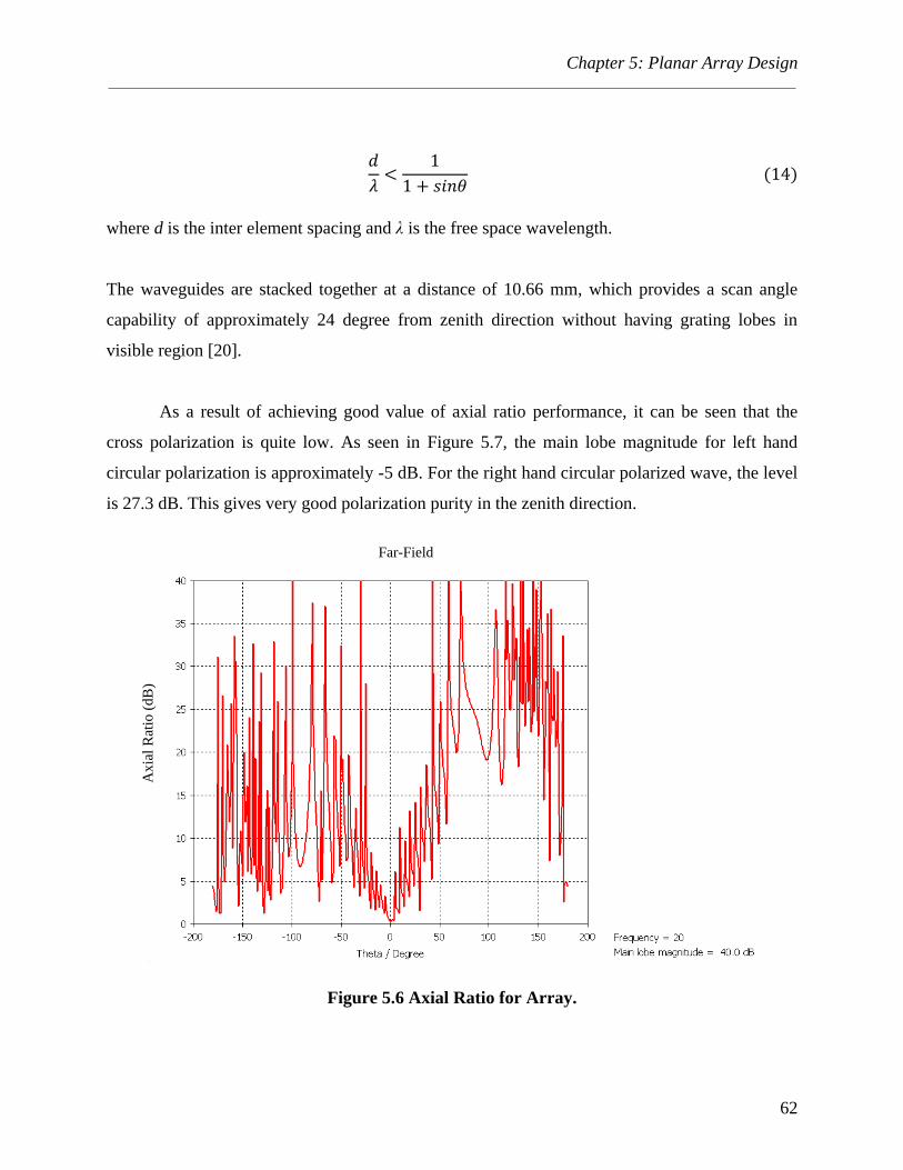
The waveguides are stacked together at a distance of 10.66 mm, which provides a scan angle
capability of approximately 24 degree from zenith direction without having grating lobes in
visible region [20].
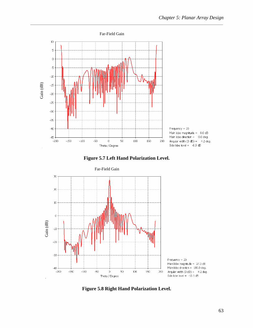
As a result of achieving good value of axial ratio performance, it can be seen that the
cross polarization is quite low. As seen in Figure 5.7, the main lobe magnitude for left hand
circular polarization is approximately -5 dB. For the right hand circular polarized wave, the level
is 27.3 dB. This gives very good polarization purity in the zenith direction.
Figure 5.6 Axial Ratio for Array.
Ax
ial
Rat
io (
dB
)
Far-Field
Chapter 5: Planar Array Design
63
Figure 5.7 Left Hand Polarization Level.
Figure 5.8 Right Hand Polarization Level.
Gai
n (
dB
)
Gai
n (
dB
)
Far-Field Gain
Far-Field Gain

Chapter 6: Measurement Results
64
Chapter 6
Measurement Results
After the simulation results were satisfied, the linear array antenna was manufactured
along with the waveguide transition as discussed in Chapter 4. In this chapter, a discussion is
provided about the fabrication of the antenna and a comparison of simulation and measurement
results is presented.
6.1 Fabrication of the Linear Array
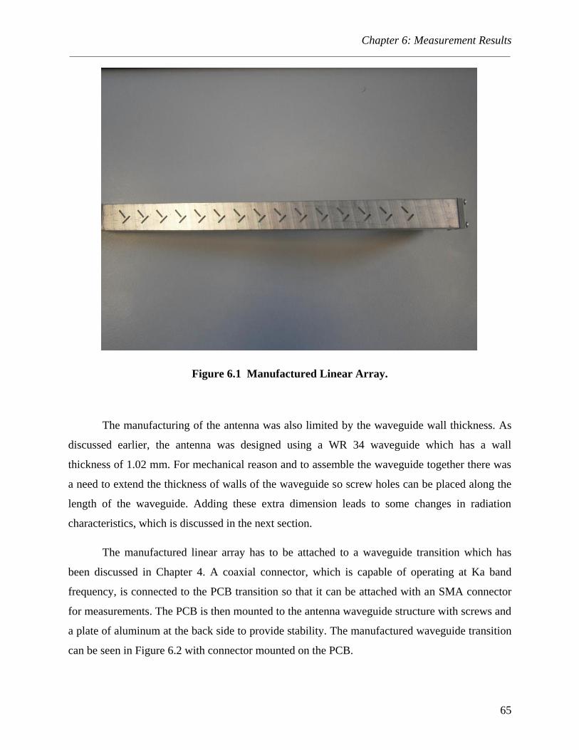
The waveguide antenna was manufactured by a high precision computer numerical control
(CNC). The reliability of the linear antenna array depends on the accuracy of the machine
because a small change in dimensions could cause significant deviation of radiation
characteristics. The manufactured antenna can be seen in Figure 6.1. The slots designed and
fabricated have a round edge rather than being purely rectangular because the slot thickness is
already 1 mm and is quite difficult to achieve pure rectangular shapes.
Chapter 6: Measurement Results
65
Figure 6.1 Manufactured Linear Array.
The manufacturing of the antenna was also limited by the waveguide wall thickness. As
discussed earlier, the antenna was designed using a WR 34 waveguide which has a wall
thickness of 1.02 mm. For mechanical reason and to assemble the waveguide together there was
a need to extend the thickness of walls of the waveguide so screw holes can be placed along the
length of the waveguide. Adding these extra dimension leads to some changes in radiation
characteristics, which is discussed in the next section.
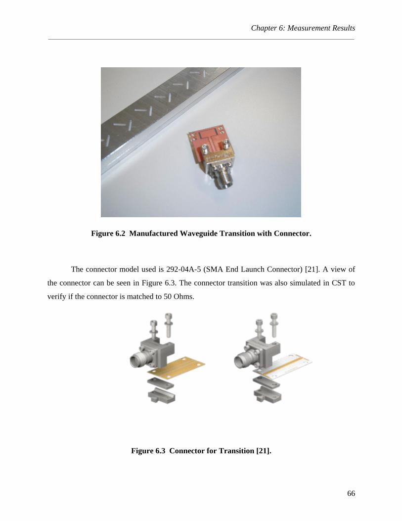
The manufactured linear array has to be attached to a waveguide transition which has
been discussed in Chapter 4. A coaxial connector, which is capable of operating at Ka band
frequency, is connected to the PCB transition so that it can be attached with an SMA connector
for measurements. The PCB is then mounted to the antenna waveguide structure with screws and
a plate of aluminum at the back side to provide stability. The manufactured waveguide transition
can be seen in Figure 6.2 with connector mounted on the PCB.
Chapter 6: Measurement Results
66
Figure 6.2 Manufactured Waveguide Transition with Connector.
The connector model used is 292-04A-5 (SMA End Launch Connector) [21]. A view of
the connector can be seen in Figure 6.3. The connector transition was also simulated in CST to
verify if the connector is matched to 50 Ohms.
Figure 6.3 Connector for Transition [21].

Chapter 6: Measurement Results
67
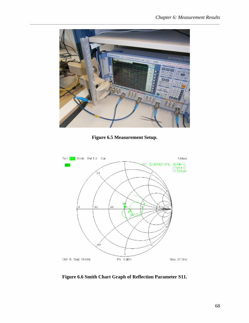
6.2 Measurements
After integration of the antenna structure with the waveguide transition, the antenna is
ready for measurements. As a first step and initial measurements, the antenna structure is put up
on a vector network analyzer R&S ZVA24 to measure the reflection parameters of the antenna as
seen in Figure 6.5. The S11 parameter can be observed in Figure 6.4. The curve shows that at our
design frequency of 20 GHz, the S11 value is -22 dB which is quite close to the simulated
results. The 10 dB bandwidth of the antenna is over 500 MHz. The matching of the antenna can
be seen in Figure 6.6.
Figure 6.4 S11 Parameter.
S1
1(d
B)
Frequency
Chapter 6: Measurement Results
68
Figure 6.5 Measurement Setup.
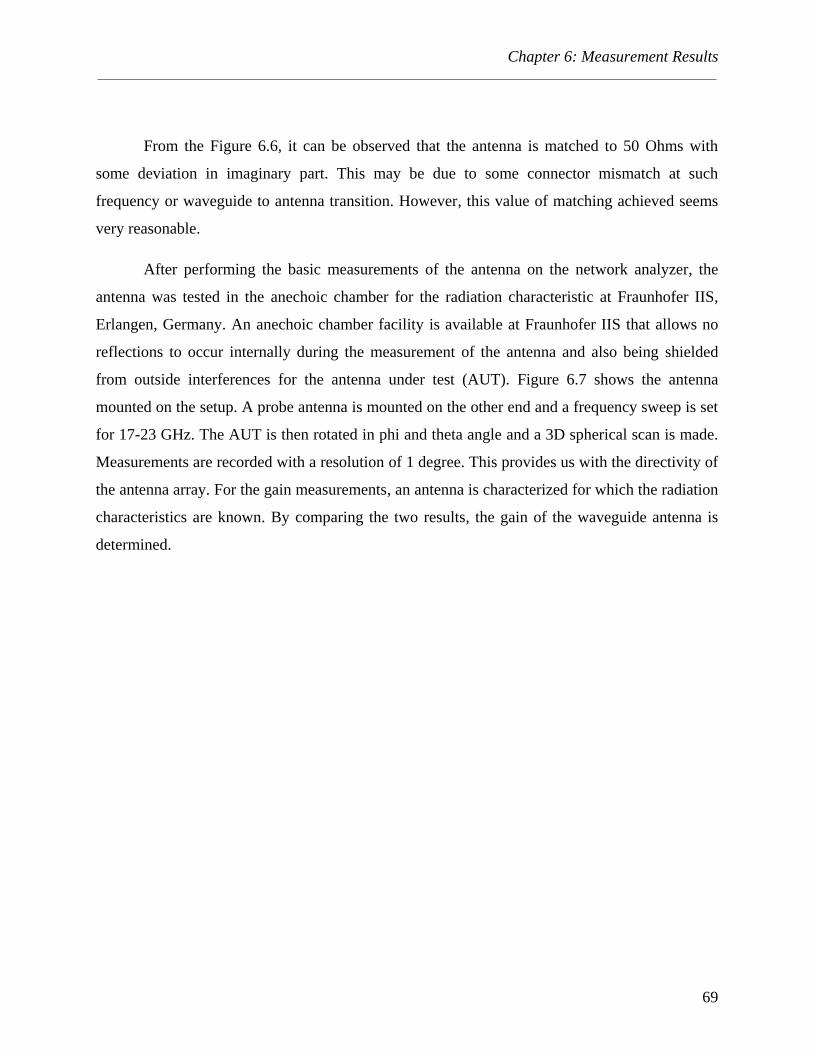
Figure 6.6 Smith Chart Graph of Reflection Parameter S11.
Chapter 6: Measurement Results
69
From the Figure 6.6, it can be observed that the antenna is matched to 50 Ohms with
some deviation in imaginary part. This may be due to some connector mismatch at such
frequency or waveguide to antenna transition. However, this value of matching achieved seems
very reasonable.
After performing the basic measurements of the antenna on the network analyzer, the
antenna was tested in the anechoic chamber for the radiation characteristic at Fraunhofer IIS,
Erlangen, Germany. An anechoic chamber facility is available at Fraunhofer IIS that allows no
reflections to occur internally during the measurement of the antenna and also being shielded
from outside interferences for the antenna under test (AUT). Figure 6.7 shows the antenna
mounted on the setup. A probe antenna is mounted on the other end and a frequency sweep is set
for 17-23 GHz. The AUT is then rotated in phi and theta angle and a 3D spherical scan is made.
Measurements are recorded with a resolution of 1 degree. This provides us with the directivity of
the antenna array. For the gain measurements, an antenna is characterized for which the radiation
characteristics are known. By comparing the two results, the gain of the waveguide antenna is
determined.
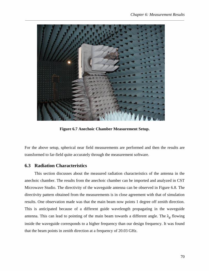
Chapter 6: Measurement Results
70
Figure 6.7 Anechoic Chamber Measurement Setup.
For the above setup, spherical near field measurements are performed and then the results are
transformed to far-field quite accurately through the measurement software.
6.3 Radiation Characteristics
This section discusses about the measured radiation characteristics of the antenna in the
anechoic chamber. The results from the anechoic chamber can be imported and analyzed in CST
Microwave Studio. The directivity of the waveguide antenna can be observed in Figure 6.8. The
directivity pattern obtained from the measurements is in close agreement with that of simulation
results. One observation made was that the main beam now points 1 degree off zenith direction.
This is anticipated because of a different guide wavelength propagating in the waveguide
antenna. This can lead to pointing of the main beam towards a different angle. The flowing
inside the waveguide corresponds to a higher frequency than our design frequency. It was found
that the beam points in zenith direction at a frequency of 20.03 GHz.

Chapter 6: Measurement Results
71
Figure 6.8 Measured 3-D Far-field Results.
Figure 6.9 Measured Far-field Directivity.
Theta/ Degree
G
ain (
dB
i)
Far-Field Gain
Chapter 6: Measurement Results
72
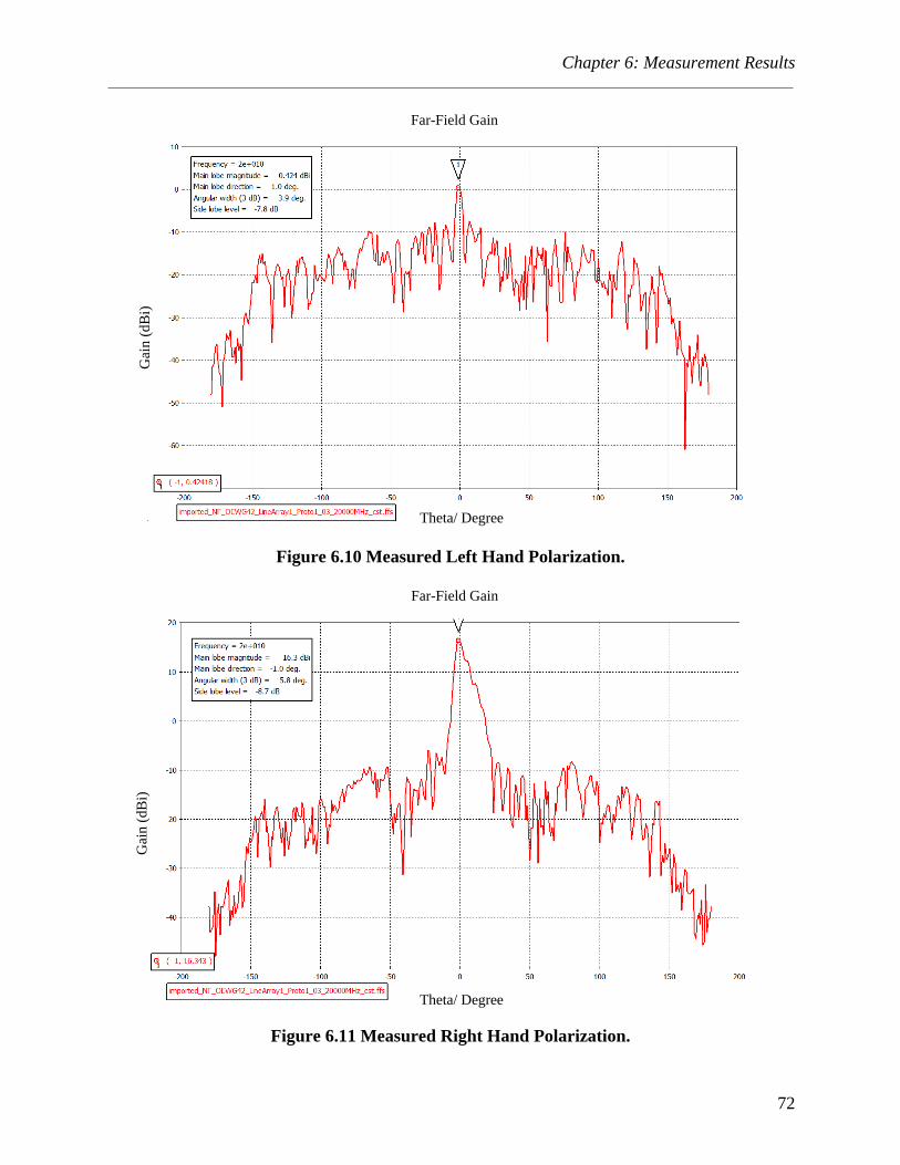
Figure 6.10 Measured Left Hand Polarization.
Figure 6.11 Measured Right Hand Polarization.
Theta/ Degree
Theta/ Degree
G
ain (
dB
i)
G
ain
(d
Bi)
Far-Field Gain
Far-Field Gain

Chapter 6: Measurement Results
73
Far-field directivity pattern, Figure 6.9 shows that the radiation characteristics are almost
the same as for the simulated antenna structure. The side lobe level achieved is -20 dB.
From Figure 6.10 and Figure 6.11 it is observed that the difference between left and right hand
polarization is around 16 dB, which suggests the antenna has good polarization characteristics.
As discussed in earlier section, thickness of waveguide walls on both sides and bottom had to be
increased so that screws can be added for assembling the structure together. This, however,
affects the performance of the antenna structure in terms of axial ratio purity. Therefore, a new
assembling technique must be looked into from the manufacturing point of view.

Chapter 7: Conclusion and Future Work
74
Chapter 7
Conclusion and Future Work
This study has shown how a quasi-planar array structure can be designed based on slotted
waveguide structures. The main focus was to investigate slot designs, based on which a circular
polarized array can be designed as most of the literature covers slot designs for linear
polarization. Cross slot structures and a recent slot topology named as offset compound slot was
investigated. Its performance was analyzed on the basis of axial ratio performance for individual
elements. Both these structures were then implemented for design of a linear array. Although
cross slot structures offer an easier design process as there are fewer variables to be optimized,
the axial ratio performance obtained is greater than 2.4 dB. On the other hand, offset compound
slot structures offer an axial ratio performance of < 0.5 dB, but several parameters have to be
considered during the design process. These linear arrays were then cascaded together to form a
planar array. It can be observed that this approach offers some advantages over conventional
existing solutions:
The design offers a low mechanical height and the structure can be mounted on a plane
surface and is well suited for nomadic applications as compared to conventional solutions
such as parabolic reflector antennas.
Chapter 7: Conclusion and Future Work
75
The other main advantage being offered is minimizing the complexity of feeding
network. As observed in microstrip based antenna arrays, the feeding network for
obtaining a circular polarized antenna array is a tedious task and meeting the design
requirements at frequency of 20 GHz is very complex [2].
From the design perspective, slotted waveguide structures offer an efficient design process
for developing a planar array. The main beam can be electronically steered in the elevation
plane by feeding the individual elements with a progressive phase shift as seen in Figure 5.3. The
azimuth plane can be controlled by a mechanical structure. Defining certain phase shifts can scan
the main beam to a designated angle. However, the scanning angle is limited because of the
grating lobe issue and maintaining high polarization purity when the beam is scanned off zenith
direction becomes difficult, especially, for low elevation angles. This is problem faced by planar
array designs.
Future work can be carried out investigating techniques which can improve the polarization
purity of the antenna array when the beam is scanned off zenith direction to a lower elevation
angle. Also, a solution has to be developed to avoid the problem of grating lobe which arises due
to limitation of reducing the inter element spacing because of the waveguide broad wall
dimensions and thickness.

76
REFERENCES
[1] M. Hein, H. Bayer, A. Kraus, R. Stephan, C. Volmer, A. Heuberger, E. Eberlein, C. Keip,
M. Mehnert, A.T. Mitschele, P. Driess, T. Volkert, ‘‘Perspectives for mobile satellite
communications in Ka-band (MoSaKa),’’ Proceedings of the Fourth European
Conference on Antennas and Propagation (EuCAP), Barcelona, Spain, 12-16 April 2010.
[2] R. C. Hansen, ‘‘Phased Array Antennas,’’ New York: Wiley Series in Microwave and
Optical Engineering, 1998.
[3] J. L. Volakis, ‘‘Antenna Engineering Handbook,’’ McGraw-Hill Professional, 4th Ed.,
2007.
[4] A. F. Stevenson, ‘‘Theory of Slots in Rectangular Wave‐Guides,’’ Journal of Applied
Physics, vol.19, no.1, pp.24-38, Jan 1948.
[5] R. S. Elliott, W. O'Loughlin, ‘‘The design of slot arrays including internal mutual
coupling,’’ IEEE Transactions on Antennas and Propagation, vol.34, no.9, pp.1149-
1154, Sep 1986.
[6] A. J. Simmons, ‘‘Circularly polarized slot radiators,’’ IRE Transactions on Antennas and
Propagation, vol.5, no.1, pp.31-36, January 1957.
[7] J. Hirokawa, M. Ando, N. Goto, N.Takahashi, T. Ojima, Uematsu, Masahiro, ‘‘A single-
layer slotted leaky waveguide array antenna for mobile reception of direct broadcast from
satellite,’’ IEEE Transactions on Vehicular Technology, vol.44, no.4, pp.749-755, Nov
1995.
[8] B. Maxum, ‘‘Resonant slots with independent control of amplitude and phase,’’ IRE
Transactions on Antennas and Propagation, vol.8, no.4, pp.384-389, July 1960.
[9] S. R. Rengarajan , ‘‘Compound radiating slots in a broad wall of a rectangular
waveguide,’’ IEEE Transactions on Antennas and Propagation, vol.37, no.9, pp.1116-
1123, Sep 1989.
77
[10] G. Montisci, G. Mazzarella, M. Musa, ‘‘A polarization-agile waveguide slot antenna,’’
IEEE Antennas and Propagation Society International Symposium, vol.3, pp.1034-1037,
22-27 June 2003.
[11] C. A. Balanis, ‘‘Antenna theory,’’ New York: John Wiley and Sons, 2nd Ed., 1997.
[12] A. J. Sangster, ‘‘Circularly polarized linear waveguide array,’’ IEEE Transactions on
Antennas and Propagation, vol.21, no.5, pp.704-705, Sep 1973.
[13] G. Montisci, M. Musa, G. Mazzarella, ‘‘Waveguide slot antennas for circularly polarized
radiated field,’’ IEEE Transactions on Antennas and Propagation, vol.52, no.2, pp.619-
623, Feb. 2004.
[14] G. Montisci, ‘‘Design of Circularly Polarized Waveguide Slot Linear Arrays,’’ IEEE
Transactions on Antennas and Propagation, vol.54, no.10, pp.3025-3029, Oct. 2006.
[15] Satellite Earth Stations and Systems (SES),ETSI EN 301 459 V1.4.1, Harmonised
European Standard (Telecommunications series), 2007.
[16] N. Dib, A. Omar, ‘‘Analysis of grounded coplanar waveguide fed patches and
waveguides,’’ IEEE Antennas and Propagation Society International Symposium, vol.4,
pp.2530-2533, 13-18 July 1997.
[17] I. J Bahl, R. Garg, P. Bhartia, ‘‘Microstrip Antenna Design Handbook,’’ Artech House,
2001.
[18] http://www.rogerscorp.com/documents/606/acm/RT-duroid-5870-5880-Data-Sheet.pdf
[19] D. Antsos, R. Crist, L. Sukamto, ‘‘A novel Wilkinson power divider with predictable
performance at K and Ka-band,’’ IEEE MTT-S International Microwave Symposium
Digest, vol.2, pp.907-910, 23-27 May 1994.
[20] R. C. Johnson, ‘‘Antenna Engineering Handbook,’’ McGraw Hill, 3 rd Ed., 1993.
[21] South West Microwave: http://mpd.southwestmicrowave.com/
[22] W. H. Watson "Resonant Slots", J. IEEE (London), vol. 93, pp.747 -777 1964.