design and implementation of quaternary nmos integrated
TRANSCRIPT

Design and Implementation of Quaternary NMOSIntegrated Circuits for Pipelined ImageProcessing
著者 亀山 充隆journal orpublication title
IEEE Journal of Solid-State Circuits
volume 22number 1page range 20-27year 1987URL http://hdl.handle.net/10097/46837

20 IEEE JOURNAL OF SOLID-STATECIRCUITS,VOL. SC-22,NO. 1, FEBRUARY1987
Design and Implementation of QuarternaryNMOS Integrated Circuits for Pipelined
Image Processing
MICHITAKA KAMEYAMA, MEMBER, IEEE, TAKAHIRO HANYU,
AND TATSUO HIGUCHI, SENIOR MEMBER, IEEE
Abstract —A new pipelined image processor using multiple-vafued logic
is effectively employed for systematic image processing without encoding
and decoding because each pixel can be dkectly expressed by a single
multiple-vafued digit for images having severat gray levels or several colors.
Furthermore, from the viewpoint of hardware implementation, reduction in
wiring complexity and reduction in chip area can be achieved in tnultiple-
vafued logic system.
In this paper, a new pattern matching pmeedure for performing four-vat-
ued image processing based on cellular logic operation is proposed, aflow-
ing two different templates to be proeessed simultaneously in a pipetined
manner. Based on these double pattern matching cells, a compact NMOS
image processing chip has been implemented. It is demonstrated that the
compactness comes from reduced interconnections in the double pattern
matching celk using a quatemary multiplexer or T gates, reatized with
pass transistors and multiple ion implants.
I. INTRODUCTION
I T HAS long been recognized that the use of multiple-
valued logic in conventional digital systems has poten-
tial advantages [1], [2]. One of the most important ad-
vantages of a multiple-valued logic system is reduction in
interconnections [3]. However, very few types of chips
based on multiple-valued logic have been fabricated for
practical applications [4]-[8].
This paper presents an implementation of a new
quaternary NMOS integrated circuit for four-valued pipe-
lined image processing using multiple ion implant tech-
nique. It has been demonstrated that not only two-valued
image processing but also several-valued image processing
is essential in applications such as robotics and medical
image processing with several colors [9], [10]. The image
processing algorithm employed here is based on cellular
logic operations which perform digitally to transform an
array of four-valued input data into a new data array.
With images having four levels or colors, each pixel can be
directly expressed by a single quaternary digit. We have
shown that by the use of quaternary logic, systematic
image processing can be effectively achieved without going
back and forth between the actual image and the binary
Manuscript received December 31, 1985; revised May 18, 1986.The authors are with the Department of Electronic Engineering, Tohoku
University, Aoba, Aramaki, Sendai 980, Japan,IEEE Log Number 8611326.
data [11]. In four-valued image processing, cellular logic
operations can be generalized by template or pattern
matching. A new pattern matching cell is designed so that
two different templates can be processed simultaneously in
a pipelined manner. The ease of this double matching
procedure is due to the full use of the quaternary informa-
tion in the matched result [12].
The image processing hardware implemented is a linear
array of the pattern matching cells which has been fabri-
cated based on the usual 10-pm NMOS process with the
unit length A = 5 pm [13], [14]. The basic building block of
the cell is a quaternary multiplexer which is also called a T
gate. The use of the T gate enables a structured design of
any quaternary logic system because both combinational
and sequential circuits can be constructed using only T
gates. The T gate consists of E/D NMOS transistors
which have different threshold voltages realized by multi-
ple ion implants. Since pass transistors are used for multi-
plexing the quaternary input signals, chip interconnections
can be greatly reduced in comparison with other imple-
mentations. The integrated T gate is proved, by measure-
ment, to have almost the desired characteristics with the
different threshold voltages, 1.2, 2.7, and 3.6 V, and a
propagation delay of 150 ns. A two-phase dynamic shift
register which can be used for the pipelined operation in
the array is also implemented using T gates. Finally, it is
confirmed that the pattern matching cell operates with a
2-MHz data rate.
Since the data flow in the array of the pattern matching
cells is completely in the form of quaternary signals, the
processing capability per unit cell is greatly increased. In
fact, the number of cells is reduced to 50 percent of a
conventional binary implementation because of the direct
processing on input pixels and the double matching proce-
dure. This implies that the interconnections between the
cells are greatly reduced.
II. IMAGE PROCESSING ALGORITHM USING
MULTIPLE-VALUED LOGIC
The digital image discussed here is uniformly sampled
and quantized to several levels.
0018 -9200/87/0200-0020 $01.00 W987 IEEE
Authorized licensed use limited to: TOHOKU UNIVERSITY. Downloaded on March 01,2010 at 22:00:59 EST from IEEE Xplore. Restrictions apply.
XAMEYAMA et al,: PIPELINEDIMAGE PROCESSING
IwlxlI
1 1I
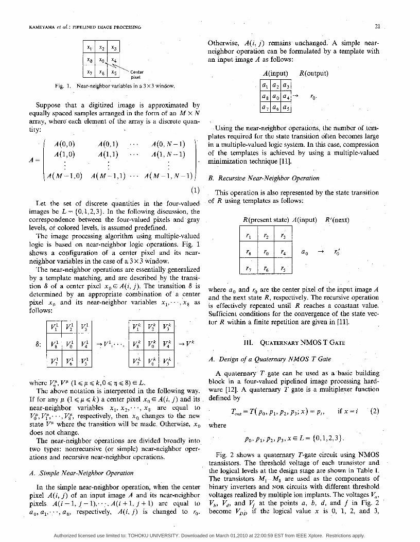
w,:,”Fig. 1. Near-neighbor variables in a 3 X 3 win
Suppose that a digitized image is approximated by
equally spaced samples arranged in the form of an M x N
array, where each element of the array is a discrete quan-
tity:
/ A(o>o) A(O,l) . . . A(O, N-1) \
A(l, O)A= .
A(l,l) . . . A(l, N–1)
\ A(M:l,O) A(M:l,l) . . . A(J4–&l) I
(1)
Let the set of discrete quantities in the four-valued
images be L = {O, 1,2,3}. In-the following discussion, the
correspondence between the four-valued pixels and gray
levels, or colored levels, is assumed predefine.
The image processing algorithm using multiple-valued
logic is based on near-neighbor logic operations. Fig. 1
shows a configuration of a center pixel and its near-
neighbor variables in the case of a 3 X 3 window.
The near-neighbor operations are essentially generalized
by a template matching, and are described by the transi-
tion 8 of a center pixel XOG A(i, j). The transition 8 is
determined by an approp;ate combination of a center
pixel XO and its near-neighbor
follows:
variables xl,. . . . xs as
+ Vk
where V;, V~(l<p<k, O<q <8)GL.
The above notation is interpreted in the following way.
If for any p (1< p < k) a center pixel XO G A(i, j) and its
near-neighbor variables xl, x ~, o. “, x ~ are equal toV$, J.7f,. . . , VJ’, respectively, then XO changes to the new
state VP where the transition will be made. Otherwise, X.
does not change.
The near-neighbor operations are divided broadly into
two types: nonrecursive (or simple) near-neighbor oper-
ations and recursive near-neighbor operations.
A. Simple Near-Neighbor Operation
In the simple near-neighbor operation, when the center
pixel A(i, j) of an input image A and its near-neighbor
pixels A(i–l, j–l), ””., A(i +1, j +1) are equal to
ao, al, . o., a g, respectively, A(i, j) is changed to ro.
21
Otherwise, A(i, j) remains unchanged. A simple near-
neighbor operation can be formulated by a template with
an input image A as follows:
A(input) R(output)
❑al az a~
a8 a. a4 -+ ro.
a7 a6 a5
Using the near-neighbor operations, the number of tem-
plates required for the state transition often becomes large
in a multiple-valued logic system. In this case, compression
of the templates is achieved by using a multiple-valued
minimization technique [11],
B. Recursive Near-Neighbor Operation
This operation is also represented by the state transition
of R using templates as follows:
R(present state) A(input) R’(next)
R
rl rz r~
r8 r. r4 a. + r;
r7 r6 r5
where a ~ and r. are the center pixel of the input image A
and the next state R, respectively. The recursive operation
is effectively repeated until R reaches a constant value.
Sufficient conditions for the convergence of the state vec-
tor R within a finite repetition are given in [11].
III. QUATERNARY NMOS T GATE
A. Design of a Quaternary NMOS T Gate
A quaternary T gate can be used as a basic building
block in a four-valued pipelined image processing hard-
ware [12]. A quaternary T gate is a multiplexer function
defined by
Tout=T(po,pl, p2,p3;~)=pi, if~=i (2)
where
PO, P1>P2>P3, X=L= {0,1,2~3}.
Fig. 2 shows a quatemary T-gate circuit using NMOS
transistors. The threshold voltage of each transistor and
the logical levels at the design stage are shown in Table I.
The transistors Ml – M8 are used as the components of
binary inverters and NOR circuits with different “threshold
voltages realized by multiple ion implants. The voltages V.,
Vb, V~, and Vf at the points a, b, d, and f in Fig. 2become VDD if the logical value x is O, 1, 2, and 3,
Authorized licensed use limited to: TOHOKU UNIVERSITY. Downloaded on March 01,2010 at 22:00:59 EST from IEEE Xplore. Restrictions apply.

22 IEEE JOURNAL OF SOLID-STATECIRCUITS,VOL. SC-22,NO. 1, FEBRUARY1987
M
-#+t!ht Wb-w=@-
&
Fig. 2. Quaternary NMOS T-gate circuit
TABLE I
PARAMETERSOFTHE DESIGNED
7’-GATE CIRCIJIT
—
respectively. Otherwise, these voltages are almost zero. The
pass tEi21SktOrS ikf15– kf~g are used as ZWdOg switches, so
that the data input pi appears at the output TOUtif the gate
voltage of the corresponding pass transistor becomes high.
By using the pass transistors, quatemary signals can be
transferred to the output without decoding to binary sig-
nals, which makes reduction in complexity of the intercon-
nections possible.
Four different enhancement-mode transistors and a de-
pletion-mode transistor are formed by using three implant
steps. ‘The enhancement-mode transistors having the
threshold voltages KA = 4 and 2 V receive boron implants
‘DS1 and ND,SZ, respectively. The depletion-mode tran-sistors having the threshold voltage V@ = – 3 V receive
phosphorus implant ND~3. The pass transistors having the
threshold voltage ~k = 1 V receive both the boron implant
N~S1 and the phosphorus implant N~~3, thus reducing thenumber of implant steps. Compared with the standard
NMOS process, the increase in the number of the implant
steps is only one. The change of the threshold voltage AVt~
can be controlled by dose control according to
A<h = q . N&/COX (3)
“DD
Tv
out
fjlkDepletion
transistorslooe -1
vout
“in C+Enhoncemmt
transistor sloDe -11,
0 ‘TCI ‘TC2‘in
(a) (b)
Fig. 3. Basic inverter. (a) E/D-tWe NMOS inverter circuit. (b) Statictransfer characteristic.
TABLE IIEXAMPLEOF VTC1 AND ‘TC2
‘th Ov 2V w I
where q is an electron charge, COXis a gate capacitance per
unit area, and N~s is the net implant dose per unit area. If
DS becomes very large, some nonlinear effects appearN
in (3).
Fig. 3 shows a basic inverter circuit used in the T gate.
Let the depletion-mode pull-up transistor have a threshold
voltage V&, and let the enhancement-mode pull-down
transistor have a threshold voltage ~fi. The switching
voltages where the slope of the curve becomes – 1 in Fig.
3(b) are given by
(4).,
where ~~ = {( WP~/LP~)/(WPU/LPU)} . (pP~/pPU), and
where pP ~, WPU, and LPU are, respectively, surface mo-
bility, channel width and length in the gate region of the
depletion-mode transistors. Similarly, pPd, Wp~, and LP~
are the corresponding parameters in the enhancement-
mode transistors. The logical threshold voltage ~..U of the
inverter is assumed to be Vi.U = ( VTC1+ VTc2)/2. In the
Custom LSI Design and Development System at Tohoku
University, the surface nobilities are measured to be pPd= 500 cm2-s-l. V-l and pPU= 375 cm2-s-l-V-l. For the
length-to-width ratio Z = 4 and V~eP= – 3 V, the voltages
v TCl~VTC2, and ~..u are given in Table II.
B. Characteristic of the Implemented T Gate
The process is based on the multiple ion implant steps
shown in Table III. The dc transfer characteristic is shown
in Fig. 4, where the output function TOUt= T(O, 1,2, 3; x) is
used as a quantizer function. The logical threshold voltages
~.~U between the logical values 1–2 and 2–3 are smaller
than the designed ones because of the nonlinear effect in
Authorized licensed use limited to: TOHOKU UNIVERSITY. Downloaded on March 01,2010 at 22:00:59 EST from IEEE Xplore. Restrictions apply.
KAMEYAMA et U/.: PIPELINEDIMAGE PROCESSING
TABLE IIIMULTIPLE ION IMPLANT QUATERNARYLOGIC
Vth(v) ImDlant Dose ( cm-z)
1 1
I 26 I ‘oron INDS=25J’
T(>ut(\
!
——
—1Transistor
i
M6 , Ml
W-+ , M8
Ml I
1% - f14
[DeDletion Tr, )
’15 ‘“18
(Pass Tr, )
“—r—————
El T t-’””’I 1
!x
(a)
1-v
=-x(v)
(b)
Fig. 4. (a) Quantizer function. (b) Static transfer characteristic of the
Input
x
output
Tout
Fig. 5.
quantizer.
21J
t—Ips
Input and output response of the quantizer.
dose control due to leakage of implants. This can be easily
improved by precise implants after the measurement of the
nonlinear effects. Fig. 5 shows a transient response. The
maximum propagation delay is about 150 ns, when the
output is connected to the control terminal ,x of another T
gate.
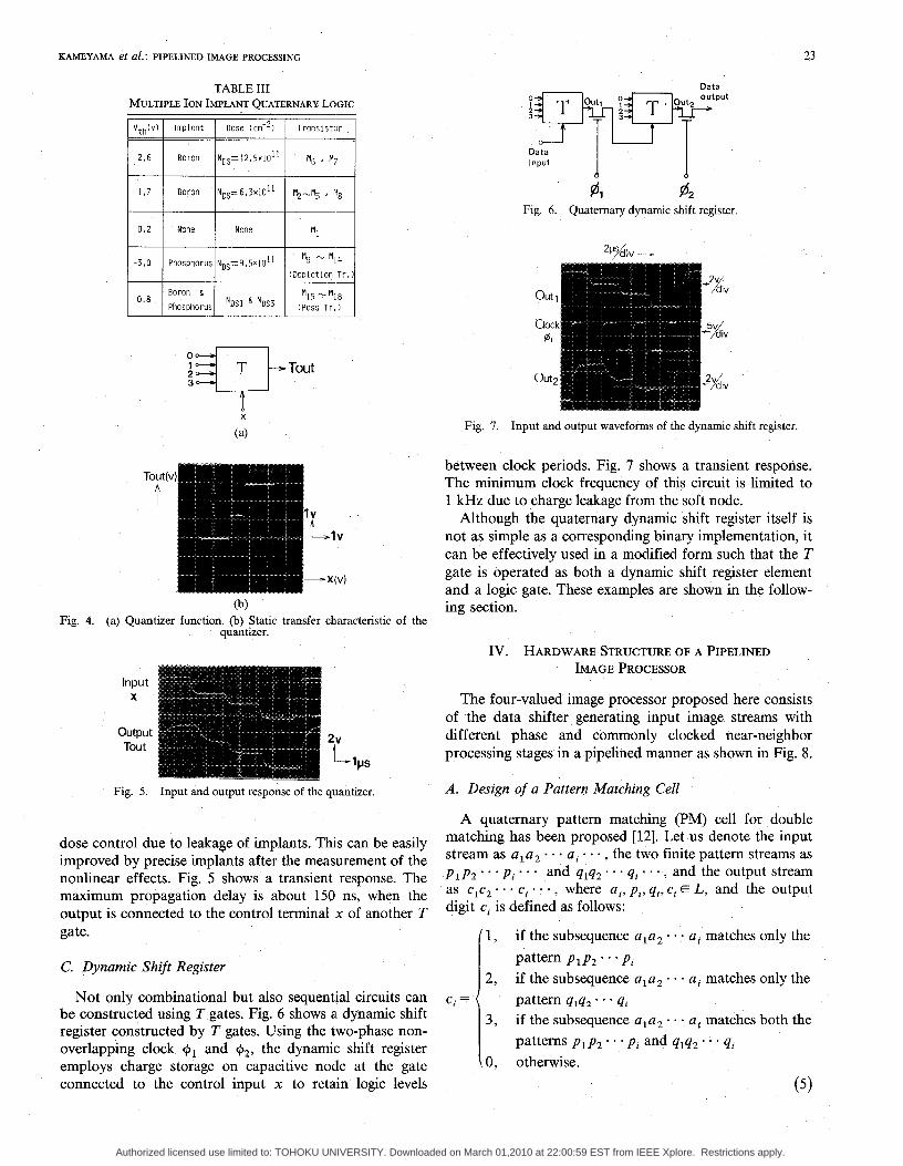
C. Dynamic Shift Register
Not only combinational but also sequential circuits canbe constructed using T gates. Fig. 6 shows a. dynamic shift
register constructed by T gates. Using the two-phase non-
overlapping clock @l and 42, the dynamic shift register
employs charge storage on capacitive nocle at the gate
connected to the control input x to retain logic levels
23
Data
‘-””’Datainput
11
0, %
Fig. 6. Quatemmy dynamic shift register.
Fig. 7. Input and output waveforms of the dynamic shift register.
between clock periods. Fig. 7 shows a transient response.
The minimum clock frequency of this circuit is limited to
1 kHz due to charge leakage from the soft node.
Although the quaternary dynamic shift register itself is
not as simple as a corresponding binary implementation, it
can be effectively used in a modified form such that the T
gate is operated as both a dynamic shift register element
and a logic gate. These examples are shown in tlhe follow-
ing section.
IV. HARDWARE STRUCTURE OF A PIPELINED
IMAGE PROCESSOR
The four-valued image processor proposed here consists
of the data shifter generating input image streams with
different phase and commonly clocked near-neighbor
processing stages in a pipelined manner as shown in Fig. 8.
A. Design of a Pattern Matching Cell
A quaternary pattern matching (PM) cell for double
matching has been proposed [12]. Let us denote the input
stream as alaz . . . ai ..0, the two finite pattern streams as
PlP2””” Pi””” andqlq2. .. q,..., and the output stream
asclcz. .. c,.,., where ai, pi, qi, Ci = L, and the output
digit Ci is defined as follows:
(1, if the subsequence alaz ~~~ai matches only the
pattern plp2” 0. pi
2, if the subsequence ala z “ “. ai matches only the
Ci =
\
pattern qlq~. . . q,
3, if the subsequence ala ~ . . . ai matches both the
\
patterns plpz o“” pi and qlqz. . . qi
O, otherwise.
(5)
Authorized licensed use limited to: TOHOKU UNIVERSITY. Downloaded on March 01,2010 at 22:00:59 EST from IEEE Xplore. Restrictions apply.

24 IEEEJOURNAL OF SOLID-STATECIRCUITS,VOL. SC-22,NO. 1, FEBRUARY1987
Pattern matcher
I I
~._.G“l-
Master cat a
Cent rol 1 shifterA
4 1
Stage 2 I
‘------l-’::
I ki:;:-:1
Fig. 8. Block diagram of the pipelined image processor.
TABLE IV
ACCUMULATORFUNCTION
\lo :i-:3
I00000
bi101012002230123
Accumulator Quantizer~--- ____ . . . . . . . . . . . . . . . .
WJ!Qlo-l..[aout
““’”’&=r-’‘n’wou’[n2
Fig. 9. Quatemary pattern matching cell.
According to this definition, two kinds of elements are
necessary to construct a quaternary PM cell. One element
is a one-dig,it comparator and the other is an accumulator.
The one-digit comparator corresponding to a pattern
matching of an input pixel can be designed easily using a
T gate:
biCT(CIO, CrI, CX2, C13; ai) (6)
where ai is the input digit operated on, and where each ai
can be determined according to the definition given in (5)
as
{
aP , = a% =3, if pi = qi
p, =1 and aq, =2,a if pi # qi (7)
all other constants aj = O.
The accumulator receives the inputs c, – 1 (the output
from the previous cell) and bi (the result from the c~m-
parator above), and h stores the accumulated matching
results of Ci _ ~ and bi. The dynamic shift register element
is also used in the accumulator for pipelined operation in
the linear array of the PM cells. The function and the
circuit diagram for this accumulator are shown in Table IV
and Fig. 9, respectively. The accumulator function can be
o—r————l
“-’*:Fig. 10. Output selector.
PM arry
[n
outIn
m :wirdow register
Fig. 11. Basic structure of the quatemary image processing hardwarefor 3 X 3 near-neighbor operations.
written as
ci=T(O, T(Ojl,Ojl ;ci_l)j T(0,0,2j2; ci-l), ci-l; bi).
(8)
Since three-stage T gates are contained in Fig. 9, the
maximum clock frequency of the cell becomes about
2 MHz. The two-phase clock 01 and +2 is used for charge
transfer. When @l is high and +2 is low, the charge
corresponding to the logic level is retained at the control
input of the T gate of the accumulator, and when @l is low
and +2 is high, the charge is transferred to the quantizer.
B. Design of an Output Selector
The specified state transition within a PM array is
performed by an output selector (OS), and the result is
stored in the dynamic shift register in the OS for the
continuous pipelined operation. Fig. 10 shows the struc-
ture of the OS using two quatemary T gates and two pass
transistors. The two-phase clock @l and +2 enables this
system to perform the image processing in a pipelined
manner synchronized with the operation of the PM cell.
C. Pipelined Image Processing Hardware
Fig. 11 shows the basic structure of quatemary image
processing hardware (pattern matcher) for 3 x 3 near-
neighbor logic operations consisting of the data shifter, the
pattern matching cells, and the output selector. The image
data transformed into serial data according to the scanning
of two-dimensional image are entered into the data shifter
through the master control processor. Shift registers in the
data shifter store two contiguous (N+ 3) pixel scan lines,
and each window register puts the image data into the
three PM cells simultaneously. All neighborhood transfor-
Authorized licensed use limited to: TOHOKU UNIVERSITY. Downloaded on March 01,2010 at 22:00:59 EST from IEEE Xplore. Restrictions apply.

~~YAW et al.: PIPELINEDIMAGk3PROCESSING 25
PM PM....—Inl . 1
PM .Input pmel
Ij’,.
N.3 ●lements . .. .
N.3 Aem+nt, IT PM amsy
.
un
f ; - - i ‘ :!$
Chtput
Inz 0 1 Ie
P M array
2 0s
:;: .,
-ddi.l
(i 0s
. . .. . . ;d[
. . . .i❑ ,le,em”t , P“yy ~&mput
Fig. 12. Structure of the quateruary image processor.
mations and data transfers are performed within a nine-
clock period.
The output image stream can be obtained at the same
rate as the input scanning, The final pattei-n matching
result of the input image is achieved by PM:5 shown in Fig.
11. Using the matching result C5 of PM5, the specified
output transition for two templates can be performed
simultazieously by the output T-gate TI as follows:
out =
4, ifc5=0
(no match)
VI, ifc~=l
(match to the first template)
v 29 ifc5=2
(match to the second template)
V1Or V2, ifc5=3
(match to both)
I3-stagelinear array of
the pattern matching
cells
______ ---- ——,-----1 1
Pattern ~ DualI;Dual
matching I multi- ,mUlti-Cell 1 plexors ;plexors
1 1
:-__- __-- .--J----
Eti(a)
(b)
Fig. 13. Fabricated NMOS chip. (a) Chip functions. (b) Chip photo-
where A, VI, and V2 are the input pixel and the state
transition values of the center pixels for two templates,
respectively.
The structure of the simple near-neighbor operation
with more than three templates is constructed by arranging
multiple PM arrays as shown in Fig. 12. The matching
result in each PM array is transformed tc~ the transition
value specified by each template in the OS which is con-
nected to a PM array. The output di of the i th OS is
determined by the matching result c: from the ith PM
array as follows:
miixograph.
(9),,3
Q!lI!F
PM PM PM
$’
L2-phose ‘--A ‘~- -i- .;- --J I
%clock ---- -b- --- -i.. ---- -1
[nrxd
(lo)
where di _ ~ is the output of the (i – l)th OS and where
V2i– 1 and V2i are the transition values for two templates
in the i th PM array.
In the case of the recursive near-neighbor operation, the
output data of the OS in the final state are fed back to the
.—.stream
out, out.2 CM3
Fig. 14. Three-stage linear array of the pattern matching cells.
master control and the timing for sending these data is
controlled by the master control processor. Then the out-
put data and the input image data are transferred into the
input nodes Inl and In z in each stage.
By the extension of the hardware arrays, pipelined image
processing for larger neighborhoods can easily be per-
formed.
V. IMPLEMENTATION OF THE IMAGE
PROCESSING HARDWARE
Fig. 13 shows the photomicrograph of the NMOS chip
using the usual rules with the unit length A = 5 pm [13].
The chip consists of a three-stage linear array of the
pattern matching cells, dual T gates, a pattern matching
cell, and the three-digit dynamic shift register. The chip
size is 5 X 4 mm2 with a total of 452 NMOS transistors.
Authorized licensed use limited to: TOHOKU UNIVERSITY. Downloaded on March 01,2010 at 22:00:59 EST from IEEE Xplore. Restrictions apply.

26 IEEE JOURNAL OF SOLID-STATECIRCUITS,VOL. SC-22,NO. 1, FEBRUARY1987
1
>%
/
Fig. 15. Input and output waveform$ of the pattern matching array.
3MO;? 1
4-valued ~ Patter” 2
i ma-
(a)
P.nern 1
ImageUJtput
,nputPcttem 2output
~ =++ ._.j
(b)
Fig. 16. Cellular arrays of pattern matching cells based on quatemaryand binary logic. (a) Quatemay hardware. (b) Binary hardware.
Figs. 14 and 15 show the circuit diagram and the
input–output waveforms of the three-stage linear array of
the pattern matching cells, where the patterns (templates)
are specified as follows:
Pattern 1: (Pi, P2, P3)=(oorl,oo’ 3,2)
Pattern 2: (~l,~2,~3)=(lor2,10r3,0).
With these patterns, the one-digit comparators become
bl=T(l,3,2,0; al) for PMl
bz=T(l,2,0,3; az) for PM2
and
b3=T(2,0,1,0; a3)for PM3
according to (7). The operating frequency of the two-phase
clock is 250 kHz in the experiment. The input stream is the
periodic waveform of Fig. 15. The output of PM3 detect-
ing Pattern 1 for (O, 3, 2) and Pattern 2 for (2,1, O) shows
clearly that the double matching is performed by the
three-stage linear array of the pattern matching cells.
TABLE V
COMPARISONOFTHEIMAGE PROCESSINGCELLULAR ARRAYS(3X 3 NEAR-NEIGHBOROPERATION)
e
TABLE VI
PARAMETERSOFTHE T-GATE CIRCUIT WITH THEPOWERSUPPLY
VOLTAGE VDD = 5 V
‘th(v)Imulont Transistors
-2,26 PhOSDhOrUS Mg - MIQ
-0,31 $
0,90 Boron M2_ M5, M8
TABLE VII
COMPARISONOFTHEPATTERNMATCHING CELLSWITH THEPOWERSUPPLYVOLTAGE VDD = 5 V
mData rate
(MHz)2,7 1.8
Fig. 16 shows a cellular logic array based on typical
binary logic components. The function of the binary array
is equivalent to that of Fig. 14. The hardware based on
binary components requires a 2-bit input for direct rep-
resentation of an input pixel and a 2-bit output for parallel
processing corresponding to the double pattern matching
procedure.
From the above discussion, the feature of the quaternary
image processing hardware is summarized as shown in
Table V. The number of cells and interconnections be-
tween cells can be reduced to 50 and 25 percent, respec-
tively. Moreover, great reduction of the number of tran-sistors can be achieved. However, the speed will be rather
slower than the binary array. From Table V, it is clear that
a highly compact chip can be realized using the quaternary
logic.
The recent dose control technique enables us to get the
threshold voltage with high precision [15]. If such precise
control is available, the power supply voltage can be made
smaller in a usual environment because the designed
threshold voltages become uniform as expec~ed and the
noise margins can be improved. For example, we can
choose V~~ = 5 V which is the same as the power supply in
a typical binary circuit. Table VI shows the logical levels
and the threshold voltage of each transistor thus specified.
Authorized licensed use limited to: TOHOKU UNIVERSITY. Downloaded on March 01,2010 at 22:00:59 EST from IEEE Xplore. Restrictions apply.
KAMEYAMA et al.: PIPELrNED IMAGE PROCESSING 27
Under these conditions, the performance of the pattern
matching cell is simulated using SPICE 2 as shown in
Table VII. It is clear that the static power dissipation can
be reduced to about half of the binary one, because of the
compactness.
VI. CONCLUSION
A new pattern matching cell which can be used in image
processing is designed and implemented using a quaternary
T gate as a basic building block. The chip k proved, by
measurement, to have almost the desired characteristics.
One of the most important advantages of the quaternary
image processing hardware is that the num”ber of the cells
can be reduced to 50 percent of the corresponding binary
implementation because of the direct processing of input
pixels and the double matching procedure. So, a highly
compact image processor can be realized by using
quatemary logic because the interconnection between the
cells can be greatly reduced, thus opening up new possibil-
ityy for future VLSI using multiple-valued logic.
ACKNOWLEDGMENT
The authors wish to thank Prof. T. Ito and Associate
Prof. M. Esashi
cdmnents.
[1]
[2]
[3]
[4]
[5]
[6]
[7]
[8]
[9]
[10]
[11]
[12]
[13]
[14]
[15]
G. Epstein, G.mukirie-valued
of Tohoku University fc)r very helpful
REFE=NCES
Frieder, and D. C. Rine, “The development oflogic as related to commrter science,” Comuuter,
vol. y, pp. 20–32, Sept. 1974.Z. G. Vranesic and K. C. Smith, “Engineering aspects of multiple-vahred logic systemsfl Computer, vol. 7? pp. 34-41,, Sept. 1974.K. C. Smith, “The p:ospects for multmlued 10SSC:A technologyand applications view,” IEEE Trans. Comput., vol. C-30,pp. 619-634, Sept. 1981.T. T. Dao. E. J. McCluskv. and L. K. Russell. “Multivaluedintegrated ‘injection logic,”” ‘IEEE Trans. Cornput., vol. C-26,pp. 1233-1241, Dec. 1977.K. W. Current, “High density integrated computing circuitry withmnltiDle valued logic,” IEEE J. So/id-State Circuits, vol. SC-15,pp. 127–131, Feb. i960.M. Stark, “Two bits per cell ROM: in Proc. COMPON, Feb.1981, pp. 209-216.M. Brilrnan, D. Etiemble, J. L. Oursel, and P. Tatareau, “A4-valued ECL encoder and decoder circuit,” IEEE J. Solid-StateCircuits, vol. SC-17, pp. 547-552, June 1982.D. A. Rich, K. C. Naiff, and K. G. Smalley, “A four-state ROMusin~ multilevel nrocess technoloxv.” IEEE J. Solid-State Circuits,vol. ~C-19, pp. 1?4–179, Apr. 19&l~K. Preston, Jr. et al., “Basis of cellular logic with some applicationsin medical image processing; Proc. IEEE, voll. 67, pp. 826-856,Mav 1979.G. j. Agin, “Computer vision systems for industrkd inspection andassembly,” Computer, vol. 13, pp. 11–20, May 1980.M. Kameyama, K. Suzuki, and T. Hlguchi, “Image processingalgorithms for a multiple-vafued array processor;’ in Proc. 13thInt. Symp. MVL, May 1983, pp. 236-241.M. Kameyama and T. Higuchi, “A new architecture of a pipelinedimage processor based on quatemary logic circuits,” in Proc. 14thInt. Symp. MVL, May 1984, pp. 92-97.C. A. Mead and L. A. Conway, Introduction to VLSI Systems.Reading, MA: Addison-Wesley, 1980.M. Kameyama et al., “AD NMOS pipelined image processor usingquatemary logic,” in Dig. IEEE Int. Solid-State Circuits Conf.,1985, WPM 8.2, pp. 86-87.A. B. Wittkower, P. H. Rose, and G. Ryding, “Advances in ionimdantation production eaui~ment,” Solid-State Technol., vol. 18.no: 12, p. 41, “Dec. 1975. - -
Michitaka Kameyama (M79) was born inUtsunomiya, Japan, on May 12, 1950. He re-ceived the B.E., M.E., and D.E. degrees in elec-tronic engineering from Tohoku University,Sendai, Japan, in 1973, 1975, and :1978, respec-tively.
He is currently an Associate Professor in theDepartment of Electronic Engineering, TohokuUniversity. His generaf research interests includemultiple-vahred logic systems, VLSI-orientedspecial-purpose processors, highly reliable digitaf
systems, and robotics.Dr. Kameyama is a member of the Institute of Electronics and Com-
munication Engineers of Japan, the Society of Instrument and ControlEngineers of Japan, the Information Processing Society of Japan, and theRobotics Society of Japan. He received the Awards for Excellence at the1984 and 1985 IEEE International Symposiums on Multiple-ValuedLogic (with T. Higucki et al.) and the Technically Excellent Award fromthe Society of Instrument and Control Engineers of Japan in 1986 (withT. Higuchi et al.). He was the Program Co-chairman of the 1986 IEEEInternational Symposium on Multiple-Valued Logic.
Takahiro Hnnyu was born in Hokkaido, Japan,on May 28, 1961. He received the B.E. and M.E.degrees in electronic engineering from TohokuUniversity, Sendai, Japan, in 1984 and 1986,respectively.
He is currently working towards the D.E. de-gree at Tohoku University. His main interestsand activities are in the multiple-valued logicsystem and its applications to artificial intelli-gence.
Mr. Hauvu is a member of the Institute ofElectronics and Communication E~gineers of Japan. He received theAward for Excellence at the 1985 IEEE International Symposium onMultiple-Valued Logic (with M. Kameyama et al.).
Tatsuo Higrrclri (M70–SM83) was born inSendai, Jamm, on March 30, 1940. He receivedthe B.E., M.E.,’ and D.E. degrees in electronicengineering from Tohoku University, Sendai,Japan, in 1962, 1964, and 1969, respectively.
He is currently a Professor with the Depart-ment of Electronic Engineering, Tohoku Univer-sity. His research interests include design of 1-Dand 2-D finite word-length digital filters, multi-ple-valued logic systems, fault-tolerant comput-ing, and VLSI computing structure for signaJ
processing and image processing.Dr. Higuchi is a member of the Institute of Electrical Engineers of
Japan, the Institute of Electronics and Communication Engineers ofJapan, and the Society of Instrument and Control Engineers of Japan. Hereceived the Awards for Excellence at the 1984 and 1985 IEEE Intern-ational Symposiums on Multiple-Valued Lo~c (with M. Kameyamaet al.), the Outstanding Transactions Paper Award from the Society ofInstrument and Control Engineers of Japan in 1984 (with M. Kwamata),and the Technically Excellent Award from the Society of Instrument andControl Engineers of Japan in 1986 (with M. Kameyama et al.). He wasthe Program Chairman of the 1983 IEEE Intemationaf Symposium onMultiple-Valued Logic, and he is the Chairman of the Japan ResearchGroup on Multiple-Valued Logic.
Authorized licensed use limited to: TOHOKU UNIVERSITY. Downloaded on March 01,2010 at 22:00:59 EST from IEEE Xplore. Restrictions apply.