design and implementation of z-source …etd.lib.metu.edu.tr/upload/12614667/index.pdfdesign and...
TRANSCRIPT

DESIGN AND IMPLEMENTATION OF Z-SOURCE FULL-BRIDGE DC/DC
CONVERTER
A THESIS SUBMITTED TO
THE GRADUATE SCHOOL OF NATURAL AND APPLIED SCIENCES
OF
MIDDLE EAST TECHNICAL UNIVERSITY
BY
AYCAN UÇAR
IN PARTIAL FULLFILLMENT OF THE REQUIREMENTS
FOR
THE DEGREE OF MASTER OF SCIENCE
IN
ELECTRICAL AND ELECTRONICS ENGINEERING
SEPTEMBER 2012

Approval of the thesis:
DESIGN AND IMPLEMENTATION OF Z-SOURCE FULL-BRIDGE DC/DC
CONVERTER
submitted by AYCAN UÇAR in partial fulfillment of the requirements for the
degree of Master of Science in Electrical and Electronics Engineering
Department, Middle East Technical University by,
Prof. Dr. Canan ÖZGEN
Dean, Graduate School of Natural and Applied Sciences
Prof. Dr. İsmet ERKMEN
Head of Department, Electrical and Electronics Engineering
Prof. Dr. Aydın ERSAK
Supervisor, Electrical and Electronics Engineering Dept., METU
Examining Committee Members:
Prof. Dr. Muammer ERMİŞ
Electrical and Electronics Engineering Dept., METU
Prof. Dr. Aydın ERSAK
Electrical and Electronics Engineering Dept., METU
Prof. Dr. Işık ÇADIRCI
Electrical and Electronics Engineering Dept., HU
Dr. Faruk BİLGİN
Space Technologies Research Institute, TUBITAK
Murat ERTEK, M.Sc. in EEE
SST, ASELSAN
Date: 11.09.2012

iii
I hereby declare that all information in this document has been obtained and
presented in accordance with academic rules and ethical conduct. I also
declare that, as required by these rules and conduct, I have fully cited and
referenced all material and results that are not original to this work.
Name, Last name : Aycan UÇAR
Signature :

iv
ABSTRACT
DESIGN AND IMPLEMENTATION OF Z-SOURCE
FULL-BRIDGE DC/DC CONVERTER
UÇAR, Aycan
M. Sc., Department of Electrical and Electronics Engineering
Supervisor: Prof. Dr. Aydın ERSAK
September 2012, 170 pages
In this work, the operating modes and characteristics of a Z-source full-bridge dc/dc
converter are investigated. The mathematical analysis of the converter in continuous
conduction mode, CCM and discontinuous conduction mode-2, DCM-2 operations
is conducted. The transfer functions are derived for CCM and DCM-2 operation and
validated by the simulation. The current mode controller of the converter is
designed and its performance is checked in the simulation. The component
waveforms in CCM and DCM-2 modes of operation are verified by operating the
prototype converter in open-loop mode. The designed controller performance is
tested with the closed-loop control implementation of the prototype converter. The
theoretical efficiency analysis of the converter is made and compared with the
measured efficiency of converter.
Keywords: Z-source, full-bridge dc/dc converter, state-space averaging method,
circuit averaging method,

v
ÖZ
Z-KAYNAKLI TAM KÖPRÜLÜ DC/DC ÇEVİRİCİ
TASARIMI VE GERÇEKLENMESİ
UÇAR, Aycan
Yüksek Lisans, Elektrik Elektronik Mühendisliği Bölümü
Tez Yöneticisi: Prof. Dr. Aydın ERSAK
Eylül 2012, 170 sayfa
Bu çalışmada Z-kaynaklı tam köprülü d.a./d.a. çeviricinin çalışma kipleri ve
karakteristiği incelenmiştir. Çeviricinin sürekli-iletim kipi ve kesikli-iletim kipi-2
operasyonları için matematiksel analizi yapılmıştır. Sürekli-iletim kipi ve kesikli-
iletim kipi-2 için türetilen transfer fonksiyonları benzetim ile doğrulanmıştır.
Çeviricinin akım döngüsü denetleci tasarlanıp, tasarlanan denetlecin benzetim
ortamında performansı incelenmiştir. Sürekli iletim kipi ve kesikli iletim kipi-2
çalışma kipleri için devre elemanları gerilim ve akım dalga biçimleri prototip
çeviricinin açık-döngü çalıştırılması ile doğrulanmıştır. Tasarlanan denetlecin
performansı prototip çeviricinin kapalı-döngü çalıştırılması ile test edilmiştir.
Çeviricinin teorik verim analizi yapılıp, çeviricinin ölçülen verimi ile
kıyaslanmıştır.
Anahtar Kelimeler: Z-kaynak, tam köprü d.a./d.a. çevirici, durum uzayı ortalama
metodu, devre ortalama metodu

vi
to My Family and Love,

vii
ACKNOWLEDGEMENTS
I would like to express my sincere thanks to my supervisor Prof. Dr. Aydın ERSAK
for his guidance, encouragement, suggestions and support throughout the thesis
study.
I wish to send a special thank to M. Tufan Ayhan for his valuable help and endless
support throughout this work. I also would like to thank Ümit Büyükkeleş, Hüseyin
Meşe, Doğan Yıldırım and Kenan Ahıska for their support.
I would like to thank Adem İleri and Gökhan Ünal for their endless support,
encouragements throughout the work.
I am grateful to ASELSAN Inc. for the funding of the hardware and facilities made
my work easier. I am indebted to TUBİTAK for the scholarship that supported my
work.
Finally, I would like to express my gratitude to my family and my love for their
encouragement and support.

viii
TABLE OF CONTENTS
ABSTRACT ................................................................................................................................ IV
ÖZ ................................................................................................................................................ V
ACKNOWLEDGEMENTS ...................................................................................................... VII
TABLE OF CONTENTS ......................................................................................................... VIII
LIST OF TABLES ....................................................................................................................... X
LIST OF FIGURES .................................................................................................................... XI
CHAPTERS
1. INTRODUCTION..................................................................................................................... 1
1.1 History ................................................................................................................................. 1
1.2 Z-Source Full-Bridge DC/DC Converter ............................................................................... 3
1.3 Scope and Outline of the Thesis ............................................................................................ 7
2. MATHEMATICAL ANALYSIS OF Z-SOURCE DC/DC CONVERTER ............................. 9
2.1 Introduction .......................................................................................................................... 9
2.2 Circuit Analysis and Simplification of Z-Source Full Bridge DC/DC Converter ................... 10
2.3 Analysis of the Simplified Model ........................................................................................ 12
2.3.1 Mathematical Analysis of Simplified Model in CCM ................................................... 13
2.3.2 Dynamic Model in CCM Operation ............................................................................. 21
2.3.3 Mathematical Analysis of Simplified Model in DCM-2................................................ 34
2.3.4 Obtaining Dynamic Model in DCM-2.......................................................................... 46
3. SIMULATION RESULTS OF Z-SOURCE DC/DC CONVERTER ..................................... 65
3.1 Introduction ........................................................................................................................ 65
3.2 Determination of the Sizes of the Energy Storage Components ............................................ 65
3.3 Simulation Results in CCM Operation................................................................................. 70
3.3.1 Verification of Circuit Components Waveforms .......................................................... 70
3.3.2 Verification of Transfer Functions ............................................................................... 73
3.4 Simulation Results in DCM-2 Operation ............................................................................. 80
3.4.1 Verification of Circuit Components Waveforms .......................................................... 80
3.4.2 Verification of Transfer Functions ............................................................................... 83

ix
4. CONTROLLER DESIGN OF Z-SOURCE DC/DC CONVERTER ...................................... 89
4.1 Introduction ........................................................................................................................ 89
4.2 Controller Design ............................................................................................................... 91
4.2.1 Current loop controller design ..................................................................................... 93
4.2.2 Voltage Loop Controller Design .................................................................................. 98
4.3 Simulation Results of the Closed-Loop System ................................................................. 102
5. EXPERIMENTAL RESULTS OF Z-SOURCE DC/DC CONVERTER ............................. 108
5.1 Introduction ...................................................................................................................... 108
5.2 The Experimental Results in Open-Loop Control .............................................................. 109
5.2.1 Open-Loop Control CCM Operation Experimental Results ........................................ 110
5.2.2 Open-Loop Control DCM-2 Operation Experimental Results ..................................... 115
5.2.3 The Efficiency of the Converter in Open-Loop Control Operation .............................. 119
5.3 The Experimental Results in Closed-Loop Control ............................................................ 120
5.3.1 The Output Voltage Regulation Against Output Loading Step Changes ...................... 121
5.3.2 Comments on the Output Voltage Responses Against Step Output Loading Changes.. 131
5.3.3 The Output Voltage Responses Against Step Changes of the Input Voltage ................ 132
5.4 The Efficiency Analysis of the Prototype Converter from Experimental Results................. 137
5.4.1 Power Loss Calculation on the Switches (MOSFETs) from the Experimental Results . 141
5.4.2 Power Loss Calculation of the Switches (Diodes) from the Experimental Results ....... 145
5.4.3 Power Loss Calculation of the Capacitors from the Experimental Results ................... 146
5.4.4 Power Loss Calculation of the Inductors from the Experimental Results..................... 147
5.4.5 Power Loss Calculation of the Isolation Transformer from the Experimenatl Results .. 151
5.4.6 Comparison of the Measured and Calculated Efficiency of the Prototype Converter ... 153
6. CONCLUSION AND FUTURE WORKS ............................................................................ 155
6.1 Conclusion ....................................................................................................................... 155
6.2 Future Works .................................................................................................................... 157
REFERENCES ......................................................................................................................... 158
APPENDICES
A. CALCULATION OF PARTIAL DERIVATIVES .............................................................. 162
B. PROTOTYPE CONVERTER CIRCUIT SCHEMATICS .................................................. 166
C. PROTOTYPE CONVERTER CIRCUIT LAYOUT ........................................................... 170

x
LIST OF TABLES
TABLES
Table 3-1 Parameters of the simulated converter for CCM operation .................... 70
Table 3-2 Parameters of the simulated converter for DCM-2 operation ................. 80
Table 4-1 Simulation Results of the Converter against Step Disturbances ........... 104
Table 5-1 Open loop control efficiency of the converter at 10% load, half load and
full-load conditions ........................................................................................ 120
Table 5-2 Definitions of the parameters used in ton and toff formula..................... 143

xi
LIST OF FIGURES
FIGURES
Figure 1-1 C-fed full-bridge dc/dc converter .......................................................... 3
Figure 1-2 Z-source impedance network ................................................................ 4
Figure 1-3 Bidirectional power flow operation ....................................................... 5
Figure 1-4 Z-source dc/dc converter with filter inductor and capacitor ................... 6
Figure 2-1 Z-source full bridge dc/dc converter .................................................... 10
Figure 2-2 Simplified circuit diagram for Z-source dc/dc converter ...................... 11
Figure 2-3 Defining electrical variables in simplified equivalent circuit for Z-source
dc/dc converter ................................................................................................. 13
Figure 2-4 Active loops during mode-1 in CCM operation of Z-source dc/dc
converter .......................................................................................................... 15
Figure 2-5 Active loops during mode-2 in CCM operation of Z-source dc/dc
converter .......................................................................................................... 16
Figure 2-6 Voltage and current waveforms regarding the circuit elements during
the CCM operation of Z-source dc/dc converter ............................................... 17
Figure 2-7 Voltage and current waveforms regarding the switching elements (Di
and Q) during the CCM operation of Z-source dc/dc converter ......................... 18
Figure 2-8 Variation of the normalized output voltage
with duty factor, D .. 21
Figure 2-9 Linearization of non-linear function at an operating point ................... 22
Figure 2-10 Active loops during mode-1 in DCM-2 operation of Z-source dc/dc
converter .......................................................................................................... 36
Figure 2-11 Active loops during mode-2 in DCM-2 operation of Z-source dc/dc
converter .......................................................................................................... 37
Figure 2-12 Active loops during mode-3 in DCM-2 operation of Z-source dc/dc
converter .......................................................................................................... 39

xii
Figure 2-13 Capacitors ( and
) and inductors ( and
) voltage and current
waveforms during the DCM-2 operation of Z-source dc/dc converter ............... 40
Figure 2-14 Switching elements (Di and Q) voltage and current waveforms during
the CCM operation of Z-source dc/dc converter ............................................... 41
Figure 2-15 Input diode voltage and current waveforms over a period .................. 48
Figure 2-16 Switch (MOSFET) waveforms over a period ..................................... 49
Figure 2-17 Rectification diode waveforms over a period ..................................... 50
Figure 2-18 Small signal ac model of the input diode ........................................... 59
Figure 2-19 Small signal ac model of the switch .................................................. 59
Figure 2-20 Small signal ac model of the rectification diode ................................ 59
Figure 2-21 Small signal ac model of the Z-source dc/dc converter in DCM-2
operation .......................................................................................................... 60
Figure 2-22 Reduced order small signal ac model of the Z-source dc/dc converter61
Figure 2-23 Small signal ac model for determination of in DCM-2
operation .......................................................................................................... 61
Figure 2-24 Small signal ac model for determination of
in DCM-2
operation .......................................................................................................... 63
Figure 3-1 Simplified circuit diagram of Z-source dc/dc converter for CCM
simulation ........................................................................................................ 70
Figure 3-2 Z-source network capacitor and output voltage in CCM ...................... 71
Figure 3-3 Input diode, Z-source network inductor and output filter inductor current
waveforms in CCM .......................................................................................... 72
Figure 3-4 Z-source network capacitor and output filter capacitor current variation
in CCM ............................................................................................................ 73
Figure 3-5 Circuit configurations simulated in order to verify ................ 74
Figure 3-6 Dynamic response of the circuit model simulated in SIMPLORER to
verify duty factor to output voltage transfer function in CCM ........................... 74
Figure 3-7 Duty factor to output voltage transfer function in CCM simulated in
SIMULINK ...................................................................................................... 76
Figure 3-8 Dynamic response of , duty factor to output voltage transfer
function in CCM obtained by SIMULINK ........................................................ 76

xiii
Figure 3-9 Circuit model simulated in SIMPLORER in order to verify input voltage
to output voltage transfer function,
.................................................... 77
Figure 3-10 Dynamic response of the circuit model for input voltage to output
voltage transfer function,
by SIMPLORER ....................................... 78
Figure 3-11 Input voltage to output voltage transfer function in CCM,
simulated in SIMULINK .................................................................................. 79
Figure 3-12 Dynamic response of input voltage to output voltage transfer function
in CCM,
simulated in SIMULINK ................................................... 79
Figure 3-13 Z-source network capacitor voltage and the output voltage in DCM-2
mode of operation............................................................................................. 81
Figure 3-14 Current waveforms belonging to input diode, Z-source network
inductor and output filter inductor in DCM-2 operation .................................... 82
Figure 3-15 Current waveforms belonging to Z-source network capacitor and
output filter capacitor in DCM-2 operation ....................................................... 83
Figure 3-16 Dynamic response of the circuit model simulated in SIMPLORER to
verify duty factor to output voltage transfer function in DCM-2 of operation .... 84
Figure 3-17 Duty factor to output voltage transfer function in DCM-2 of operation
simulated in SIMULINK .................................................................................. 85
Figure 3-18 Dynamic response of , duty factor to output voltage transfer
function in DCM-2 mode of operation obtained by SIMULINK ....................... 85
Figure 3-19 Dynamic response of the circuit model simulated by SIMPLORER to
verify input voltage to output voltage transfer function in DCM-2 mode of
operation .......................................................................................................... 86
Figure 3-20 Input voltage to output voltage transfer function in DCM-2 mode of
operation simulated in SIMULINK................................................................... 87
Figure 3-21 Dynamic response of
, input voltage to output voltage transfer
function in DCM-2 mode of operation obtained by SIMULINK ....................... 87
Figure 4-1 Control block diagram of the converter ............................................... 92
Figure 4-2 Current loop control block diagram ..................................................... 93
Figure 4-3 Pole-zero map of ................................................................. 95

xiv
Figure 4-4 Bode diagram of .................................................................. 96
Figure 4-5 Bode diagram of the compensated open-loop transfer function of current
loop .................................................................................................................. 98
Figure 4-6 Voltage loop control block diagram .................................................... 99
Figure 4-7 Pole-zero map of ................................................................ 100
Figure 4-8 Bode diagram of the compensated open-loop transfer function of
voltage loop.................................................................................................... 101
Figure 4-9 Pole-zero map of .................................................................... 102
Figure 4-10 Closed-loop simulation model of Z-source dc/dc converter ............. 103
Figure 4-11 Output voltage during full-load-to-10% load-to-full-load transition
under 32V input voltage ................................................................................. 105
Figure 4-12 Output voltage during full-load-to-10% load-to-full-load transition
under 18V input voltage ................................................................................. 105
Figure 4-13 Output voltage during 18V-to-32V-to-18V input voltage transition
under full-load ................................................................................................ 106
Figure 4-14 Output voltage during 18V-to-32V-to-18V input voltage transition
under 10% load .............................................................................................. 106
Figure 5-1 Top view of the prototype converter .................................................. 109
Figure 5-2 Bottom view of the prototype converter ............................................ 109
Figure 5-3 Voltage and current waveforms of against applied PWM in CCM 110
Figure 5-4 Voltage and current waveforms of against applied PWM in CCM 112
Figure 5-5 voltage waveform against applied PWM in CCM, a) dc coupling, b)
ac coupling ..................................................................................................... 113
Figure 5-6 Output voltage waveform against applied PWM in CCM, a) dc
coupling, b) ac coupling ................................................................................. 114
Figure 5-7 a) anode-cathode, b) isolation transformer primary side, c)
cross-pair voltage waveforms against applied PWM in CCM ............. 115
Figure 5-8 Lz current and voltage waveform against applied PWM in DCM-2 ... 116
Figure 5-9 Lo current and voltage waveform against applied PWM in DCM-2 ... 117
Figure 5-10 voltage waveform against applied PWM in DCM-2, a) dc coupling,
b) ac coupling ................................................................................................. 118

xv
Figure 5-11 The output voltage waveform against applied PWM in DCM-2, a) dc
coupling, b) ac coupling ................................................................................. 118
Figure 5-12 a) anode-cathode, b) isolation transformer primary side, c)
cross-pair voltage waveforms against applied PWM in DCM-2 ......... 119
Figure 5-13 The output voltage response of the converter against a step change of
loading from 0.2 A to 1.5 A for Vs=20 V ........................................................ 122
Figure 5-14 The output voltage response of the converter against a step change of
loading from 0.2 A to 1.5 A for Vs=30 V ........................................................ 123
Figure 5-15 The output voltage response of the converter against a step change of
loading from 1.5 A to 0.2 A for Vs=20 V ........................................................ 124
Figure 5-16 The output voltage response of the converter against a step change of
loading from 1.5 A to 0.2 A for Vs=30 V ........................................................ 125
Figure 5-17 The output voltage response of the converter against a step loading
from 1.5 A to 3 A for Vs=20 V ....................................................................... 126
Figure 5-18 The output voltage response of the converter against a step loading
from 1.5 A to 3 A for Vs=30 V ....................................................................... 126
Figure 5-19 The output voltage response of the converter against a step unloading
from 3 A to 1.5 A for Vs=20 V ....................................................................... 127
Figure 5-20 The output voltage response of the converter against a step unloading
from 3 A to 1.5 A for Vs=30 V ....................................................................... 128
Figure 5-21 The output voltage response of the converter against a step increase of
loading from 0.2 A to 3 A for Vs=20 V ........................................................... 129
Figure 5-22 The output voltage responses of the converter against a step increase of
loading from 0.2 A to 3 A for Vs=30 V ........................................................... 129
Figure 5-23 The output voltage response of the converter against a step unloading
from 3 A to 0.2 A for Vs=20 V ....................................................................... 130
Figure 5-24 The output voltage response of the converter against a step unloading
from 3 A to 0.2 A for Vs=30 V ....................................................................... 131
Figure 5-25 The output voltage response of the converter against a step change of
the input voltage from 20 V to 30 V for iLoad=0.2 A ........................................ 133

xvi
Figure 5-26 The output voltage response of the converter against a step change of
the input voltage from 20 V to 30 V for iLoad=1.5 A ........................................ 134
Figure 5-27 The output voltage response of the converter against a step change of
input voltage from 20 V to 30 V for iLoad=3 A ................................................ 134
Figure 5-28 The output voltage response of the converter against a ramp input
voltage decay from 30 V to 20 V for iLoad=0.2 A............................................. 135
Figure 5-29 The output voltage response of the converter against a ramp input
voltage decay from 30 V to 20 V for iLoad=1.5 A............................................. 136
Figure 5-30 The output voltage response of the converter against a ramp input
voltage decay from 30 V to 20 V for iLoad=3 A ............................................... 137
Figure 5-31 Defining electrical variables for efficiency analysis of Z-source dc/dc
converter ........................................................................................................ 138
Figure 5-32 Determination of current waveform magnitudes regarding the circuit
elements for open-loop control ....................................................................... 139
Figure 5-33 Determination of current waveform magnitudes regarding the circuit
elements for open-loop control ....................................................................... 140
Figure B-1 Sheet 1 of the prototype converter circuit schematics........................ 166
Figure B-2 Sheet 2 of the prototype converter circuit schematics........................ 167
Figure B-3 Sheet 3 of the prototype converter circuit schematics........................ 168
Figure B-4 Sheet 4 of the prototype converter circuit schematics........................ 169
Figure C-1 Top side layout of the prototype converter........................................ 170
Figure C-2 Bottom side layout of the prototype converter .................................. 170

1
CHAPTER 1
INTRODUCTION
1.1 History
Dc power supplies are mainly utilized to meet the power needs of electrical
and electronics equipments. The required output voltage can be produced either by a
linear voltage regulator, LVR or a switch mode power supply, SMPS.
LVRs have some certain advantages such as simplicity of design and low
level noise since no switching element exists in LVR topology. However, boosting
the input voltage is not possible with LVR topology. Moreover, isolation cannot be
achieved. Inefficiency is the main drawback of LVRs, which makes it unsuitable for
the applications where the required output voltage is not close to the unregulated
input voltage, or the unregulated input voltage varies within a wide range.
SMPS topologies have several advantages relative to LVRs such as higher
efficiency within wide operating range, smaller sizes of energy storage components
and lower weight of the converter. Furthermore, buck and/or boost operations and
isolation between the input and output voltage can be achieved with SMPS.
The buck and boost converters are the two basic SMPS topologies, from
which all other SMPS topologies can be derived [1]. They can be separated into two
groups as isolated and non-isolated. In many applications the isolation between the

2
input voltage and output voltage is required due to safety issues. The traditional
boost converter cannot be used in the applications where isolation is required.
Flyback converter is the most popular transformer based boost converter
topology. Very high efficiencies can be achieved with flyback. However, due to its
topology, the primary side of the isolation transformer always sees a positive voltage,
resulting in always in the same direction flux in the core. This phenomenon limits the
amount of power to be transferred by the isolation transformer, and therefore the
output power rating of the converter [2]. Hence, flyback topology is generally
preferred up to 100-150W.
The traditional transformer isolated high power dc/dc conversion circuit is
full-bridge converter. The full-bridge converter can be voltage-fed (V-fed) or
current-fed (C-fed).
V-fed full-bridge converter is a buck derived topology. Hence, it is not
possible to obtain a higher output voltage unless using a step-up transformer for the
isolation. In [3] it is mentioned that, higher transformer turns ratio leads to higher
leakage inductance resulting in excessive ringing on the rectifier diodes. [4] states
that ringing decreases the efficiency of the converter. Besides efficiency concern, the
severe ringing shortens the life time of rectifier diodes, hence decreases reliability of
the converter. The current drawn from the input power supply increases as the turns
ratio increases according to [5]. This results in higher conduction loss on the parasitic
of the converter, hence decreasing the efficiency; and higher current carrying capable
switches to be used in the converter, thus raising the cost of the converter.
The C-fed full-bridge converter can be used for boosting operation. The
output voltage of the C-fed full-bridge converter is always greater than the input
voltage. Hence, the C-fed full-bridge converter is not preferred for wide input
voltage range operations. The traditional C-fed full-bridge converter is displayed in
Figure 1-1. The most commonly known problem of C-fed full-bridge converter is the
voltage overshot problem in the primary switches, due to the leakage inductance of
the isolation transformer [6]. Another limitation for the C-fed converter is that one of

3
the upper switches (Q1, Q3) and one of the lower switches (Q2, Q4) have to be gated
on and maintained on together at any time as mentioned in [7]. In other words, the
current flowing through the inductor, must always find a path to flow. In C-fed
full-bridge converter the path has to be provided by the proper gating on the switches
in full-bridge part. If at least one of the upper switches and one of the lower switches
fail to conduct, which might be due to EMI noise, switch failure or drive circuitry
failure, during the operation the dc inductor would then be open-circuited [7]. This
might destroy the switches in the full-bridge part, since the energy stored on the dc
inductor is dissipated on the switches. The open circuit problem of the C-fed full-
bridge is a major concern regarding the converter’s reliability [8], [9].
Figure 1-1 C-fed full-bridge dc/dc converter
The aforementioned limitation and problems of the C-fed full-bridge
converter can be solved by Z-source topology.
1.2 Z-Source Full-Bridge DC/DC Converter
The Z-source network impedance is shown in Figure 1-2. Z-source network is
used to couple the converter/inverter main circuitry to the power source.
VS
Q1
Q2
Q3
Q4
CO RL
+
VO
-
D1
D2
D3
D4
L
is(t)

4
Figure 1-2 Z-source impedance network
Z-source network can be used in each type of power conversion; that is ac/ac,
ac/dc, dc/ac and dc/dc. The operation principles of the Z-source network for the
inverters are investigated in detail in [8]. The theoretical limitations and drawbacks
of the traditional voltage-source and current-source inverters are discussed in this
work. In voltage-source inverters the switches on the same half-bridge cannot be
turned on at the same time and the output voltage cannot exceed the input voltage
(buck derived). In the current-source inverters, the output voltage is always greater
than the input voltage (boost derived) and at least one of the upper and one of the
lower switches must be ‘ON’ at the same time. Z-source eliminates these problems
and makes it possible to use the inverter in a step-up or step-down manner.
Some discusses the ac/ac power conversion with Z-source network
impedance [10]. The Z-source impedance is connected to the ac power source.
Adjustable speed drive implementation is conducted in this work. It is shown that
when duty factor is less than 0.5 the inverter works in buck mode, and when duty
factor is greater than 0.5 the inverter work in boost mode.
For the dc/dc converter implementations main studies are addressed in [7],
[11]-[14]. In [7] the Z-source impedance network is composed of an array of
inductors and capacitors. The impedance network contains two conductors with
dielectric insulation to form capacitance and two current carrying conductors
insulated by magnetic core to form inductance. The output voltage of the converter is
controlled by changing the switching frequency. In normal operation all the switches
CZ2
LZ1
LZ2
CZ1DC
SOURCE
CONVERTER/
INVERTER
5
have a duty cycle of 0.5. For boosting the input voltage short circuit duty cycle is
increased, that is the switches on the same phase leg are gated on simultaneously
(short circuit the phase leg). For buck operation open-circuit duty ratio is increased,
so that the switches on the same phase leg are gated off simultaneously (open circuit
the phase leg).
Another report discusses the Z-source resonant dc/dc converter structure [11].
This work is a follow-up of the study in [7]. The Z-source network is replaced by the
qZ-source structure so that the sizes of the energy storage elements are reduced,
which in turn reduces the cost and weight of the converter. The output voltage is kept
constant at 100 V while the input voltage varies between 50-150 V by changing the
switching frequency of the converter.
In [12] a novel Z-source dc/dc converter topology is proposed. In this
topology the isolation between input and output does not exist. The prototype
converter is designed for an electric vehicle application. The input diode is replaced
by a switch, MOSFET. The topology allows bidirectional power flow. Considering
the power source as a dc voltage source, power flows from the source to the load
side. When the vehicle needs to be braked the power flows from load to power
source. The power flow direction and the switches operating during the operating
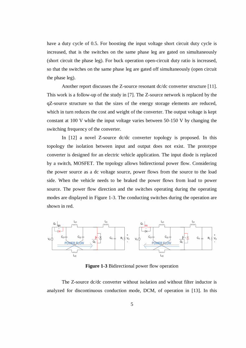
modes are displayed in Figure 1-3. The conducting switches during the operation are
shown in red.
Figure 1-3 Bidirectional power flow operation
The Z-source dc/dc converter without isolation and without filter inductor is
analyzed for discontinuous conduction mode, DCM, of operation in [13]. In this
VS
CZ1 CZ2
LZ1
LZ2
Q2
LO
CO RL
+
VO
-
Q1
POWER FLOW
VS
CZ1 CZ2
LZ1
LZ2
Q2
LO
CO RL
+
VO
-
Q1
POWER FLOW

6
work, it is assumed that DCM operation starts when the Z-source inductor current
falls to zero. Only the input voltage-output voltage relationships are derived and the
critical Z-source inductor value calculation is done in this work.
A well organized and detailed investigation of the operating modes and
operation of Z-source dc/dc converter with filter inductor and filter capacitor is
conducted in [14]. The analyzed circuit is shown in Figure 1-4.
Figure 1-4 Z-source dc/dc converter with filter inductor and capacitor
In [14] it is stated that the converter can operate in CCM or DCM operation.
There are three different DCM and one CCM of operation for the analyzed converter.
CCM Operation: The current through the input diode, Di and rectifier
diode, Dr does not fall to zero in their switching time intervals.
DCM-1 Operation: The current through the input diode, Di falls to
zero in its switching time interval, but rectifier diode, Dr does not fall
to zero in its switching time interval.
DCM-2 Operation: The current through the input diode, Di does not
fall to zero in its switching time interval, but rectifier diode, Dr falls to
zero in its switching time interval.
DCM-3 Operation: The current through the input diode, Di and
rectifier diode, Dr fall to zero in their switching time intervals.
In [14] all the input voltage-output voltage relationships and the necessary
transfer function of the converter are derived for CCM and DCM-1 operations. All
VS
Di
CZ1 CZ2
LZ1
LZ2
Q
LO
CO RL
+
VO
-
Dr

7
the verifications of the voltage relationships and transfer functions are provided in
[14]. Voltage mode control of the produced prototype converter is implemented.
1.3 Scope and Outline of the Thesis
In this thesis a Z-source full-bridge dc/dc converter is designed and
implemented. The CCM and DCM-1 operation of the converter have been analyzed
before [14]. In this work, the converter is designed so as to operate in CCM and
DCM-2 operations.
The thesis contains six chapters. In the second chapter, the input voltage-
output voltage relationships and the necessary transfer functions of the converter for
CCM and DCM-2 operation are derived. The mathematical analysis of the converter
in DCM-2 operation developed in this thesis study is an original contribution to the
literature. The derived transfer functions and input voltage-output voltage
relationships are verified by simulation in the third chapter. Circuit level simulations
are made in SIMPLORER, while the transfer functions of the converter are verified
in SIMULINK.
The controller design of the converter is done in Chapter 4. The current mode
control design is made with the help of MATLAB for determining the phase and gain
margins of the closed-loop controlled converter. The current mode control
implementation and the controller design given in this thesis as another original
contribution to the literature. The controller implemented in digital control form is an
extension of this last original contribution. The closed-loop system simulation results
given in the fourth chapter can also be seen as a contribution.
The fifth chapter is composed of the experimental results obtained from the
produced prototype converter. The converter is operated in open-loop control to
verify the component waveform simulations result. In order to examine the designed
controller performance the converter is operated in closed-loop control. The output
voltage regulation against applied disturbances is investigated. A comparison of the
simulation and experimental results is given in this chapter. In the fifth chapter, the

8
efficiency analysis of the converter is also conducted. The calculated and measured
efficiencies are compared in the efficiency analysis part.
The last chapter is a concluding chapter which proposes possible future
works.

9
CHAPTER 2
MATHEMATICAL ANALYSIS OF Z-SOURCE DC/DC
CONVERTER
2.1 Introduction
The theoretical analysis of Z-source dc/dc converter has been examined in
detail with ideal elements before [14]. The analysis introduced here establishes input
and output voltage relationships both for continuous conduction mode (CCM) and
discontinuous conduction mode-1 (DCM-1) operational conditions. For a design and
implementation process such analyses are to be done.
The converter is designed here so as to work in CCM and DCM-2 and the
converter operating in these modes has not been analyzed before. In this chapter this
task, the mathematical analysis of the converter operating in CCM and DCM-2 will
be accomplished. The input-output voltage relation is established for both modes of
the converter operation. In addition the input voltage-to-output voltage and duty
factor-to-output voltage transfer functions are derived for both operation modes. The
state space averaging technique is utilized for the transfer function analysis of the
converter in CCM operation. For DCM-2 operation analysis, the circuit averaging
technique is used. The boundary condition for the transition between CCM and
DCM-2 operations is also established in this chapter.

10
2.2 Circuit Analysis and Simplification of Z-Source Full Bridge
DC/DC Converter
The Z-source full bridge dc/dc converter is utilized in order to boost the input
voltage to the higher output voltage level in applications. The circuit diagram of the
converter is basically as shown in Figure 2-1.
Figure 2-1 Z-source full bridge dc/dc converter
Apparently the Z-source network is used to adjust the dc voltage level seen
across the full bridge MOSFETs. In order to boost the voltage at the input terminals
of full bridge, the MOSFETs in the same half bridge must be gated on
simultaneously. Thus, either Q1 and Q2, or Q3 and Q4 must be turned on
simultaneously. In literature this is known as shoot-through state [8]. Generally all
the MOSFETs in the full bridge are turned on at the same time for boosting operation
in order to apply equal stress on the MOSFETs to prevent an early MOSFET failure
or degradation of electrical characteristics [15]. In this way the current passing
through the MOSFETs during the shoot through state is shared between the two half
bridges. This enables the designer to use MOSFETs with lower current rating in the
design leading to a cost effective solution. During the shoot-through state the Z-
source network inductors are energized by the Z-source network capacitors.

11
The full bridge part is necessary for the isolation and rectification. By the
switching pattern of the MOSFETs an ac voltage is generated across the primary
terminals of the isolation transformer. The ac voltage transferred to the secondary
side by the transformer action is rectified by the use of rectification diodes.
Furthermore the rectification diodes prevent the energy flow from the output filter
capacitor Co to the primary side of the transformer.
The last block in Figure 2-1 is utilized to diminish the ripples observed on the
output voltage and the current waveforms.
The full bridge section in the Z-source converter can be simplified in order to
simplify the mathematical analysis of converter to some extent. Note that when all
full bridge MOSFETs are turned on during shoot-through state, the primary of the
transformer is shorted in this state. In the next switching cycle, only one of the
MOSFETs is going to be left conducting in each phase leg. Considering this fact the
full bridge MOSFETs and diodes can be replaced by a single MOSFET and a single
diode by removing the isolation transformer. In this manner all the functional
features of the converter is kept as they are, and the mathematical analysis, however,
becomes much simple. The only difference between the simplified Z-source dc/dc
converter and the actual full bridge dc/dc converter is the loss of isolation between
the input and the output. The simplified circuit diagram of the Z-source dc/dc
converter is given in Figure 2-2.
Figure 2-2 Simplified circuit diagram for Z-source dc/dc converter
VS
Di
CZ1 CZ2
LZ1
LZ2
Q
LO
CO RL
+
VO
-
Dr

12
2.3 Analysis of the Simplified Model
In this part the input voltage-output voltage relations and the transfer
functions of the circuit are derived in terms of duty factor, D, and the components of
the circuit, i.e. inductors, capacitors and load resistance. The analysis is made for
both CCM and DCM-2 operations.
In literature the Z-source network inductors are set equal to each other, which
is also the case for capacitors. By this way symmetrical voltage waveforms are
obtained on Z-source inductors. In addition to that the current waveforms obtained
on Z-source capacitors come out identical over the switching period [8], [9]. Hence
by setting the Z-source network inductors and capacitors as in (2.1), it can be
concluded that the equalities given in (2.2) hold.
(2.1)
(2.2)
13
In (2.2) the upper case letters represent the dc values of the voltages and
currents of Z-source inductors and capacitors. The lower case letters with on top
represent the small signal values of currents and voltages.
2.3.1 Mathematical Analysis of Simplified Model in CCM
Considering the simplified circuit diagram of Z-source dc/dc converter we
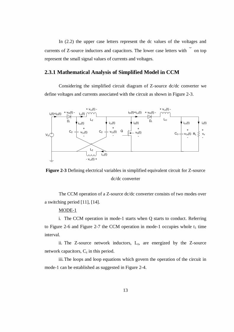
define voltages and currents associated with the circuit as shown in Figure 2-3.
Figure 2-3 Defining electrical variables in simplified equivalent circuit for Z-source
dc/dc converter
The CCM operation of a Z-source dc/dc converter consists of two modes over
a switching period [11], [14].
MODE-1
i. The CCM operation in mode-1 starts when Q starts to conduct. Referring
to Figure 2-6 and Figure 2-7 the CCM operation in mode-1 occupies whole t1 time
interval.
ii. The Z-source network inductors, Lz, are energized by the Z-source
network capacitors, Cz in this period.
iii. The loops and loop equations which govern the operation of the circuit in
mode-1 can be established as suggested in Figure 2-4.
VS
Di
CZ CZ
LZ
LZ
Q
LO
CO RL
+
vo
-
Dr
is(t)=iDi(t)+ vDi(t) -
iCz(t)
+
vCz(t)
-
iCz(t)
+
vCz(t)
-
+ vLz(t) -
iLz(t)
iQ(t)
+
vQ(t)
-
+ vDr(t) -iDr(t)=iLo(t)+ vLo(t) -
+
vCo(t)
-
iCo(t) io(t)
iLz(t)
- vLz(t) +

14
iv. Applying the Kirchhoff’s voltage law around LOOP-2 shown in Figure
2-4, the voltage across the Z-source network inductor during t1 time interval
yields;
. (2.3)
v. Applying the Kirchhoff’s voltage rule around LOOP-1 shown in Figure
2-4, the voltage across the input diode Di during t1 time interval yields;
. (2.4)
vi. For the boosting operation of the converter the Z-source network capacitor
voltage is equal to output voltage as;
(2.5)
The equality stated in (2.5) is proven at (2.16) and (2.18). Considering (2.4)
and (2.5), and the fact that the converter is boosting the input voltage, i.e.
, it can be concluded that the input diode voltage is negative during t1,
hence Di is not conducting implying that no current is drawn from the input supply
during the period.
vii. Thus, during t1, the output filter elements Lo and Co supply the required
energy to the load. Note that, the energy to the load is supplied via Lo, hence the
rectification diode Dr is conducting during the time interval.
viii. Note that, the Kirchhoff’s voltage law around LOOP-3 yields;
. (2.6)

15
Figure 2-4 Active loops during mode-1 in CCM operation of Z-source dc/dc
converter
MODE-2
i. Let Ts represent a full switching period for the converter while running at
steady state. The CCM operation in mode-2 starts at time DTs where D is called as
the duty factor applied to Q. At that instant, Q is turned off and stops conducting.
ii. The loop equations regarding to mode-2 operation can be written referring
to the circuit shown in Figure 2-5.
iii. Applying the Kirchhoff’s voltage law around LOOP-1 shown in Figure
2-5, the voltage across the filter inductor Lo, during mode-2 is found as;
. (2.7)
From (2.5) and (2.7) the filter inductor voltage can be written as;
. (2.8)
Recall that for boosting operation, hence the filter inductor
voltage in mode-2 for CCM operation is positive implying that it stores
energy during this time interval.
iv. Applying the Kirchhoff’s voltage law around LOOP-2 shown in Figure
2-5, the voltage across Lz during mode-2 is found as;
VS
Di
CZ CZ
LZ
LZ
Q
LO
CO RL
+
vo
-
Dris(t)=iDi(t)+ vDi(t) -
iCz(t)
+
vCz(t)
-
iCz(t)
+
vCz(t)
-
+ vLz(t) -
iLz(t)
iQ(t)
+
vQ(t)
-
+ vDr(t) -
iDr(t)=iLo(t)
+ vLo(t) -
+
vCo(t)
-
iCo(t) io(t)
iLz(t)
LOOP-1
- vLz(t) +
LOOP-2 LOOP-3

16
. (2.9)
From (2.5) and recalling the fact that , it is obvious that
is negative during mode-2 for CCM operation. As a result, the energy stored in Lz in
mode-1 is transferred to the load in mode-2.
v. The negative polarity of on Lz forces the input diode Di to conduct.
vi. Finally the current circulating around LOOP-1, shown in Figure 2-5,
charges Cz.
Figure 2-5 Active loops during mode-2 in CCM operation of Z-source dc/dc
converter
For further details in the mathematical analysis and to find input voltage-
output voltage relationship some assumptions must be made at this point. The first, is
that the capacitor sizes are supposed to be chosen large enough so that the ripple
voltage across them over a period is negligible [7], [14]. The second is that the input
voltage is ripple free and remains constant over a period, Ts. With these two
assumptions the capacitor voltages and input voltage can be accepted as dc voltages
for the rest of the analysis. Thus we define the followings;
(2.10)
.
VS
Di
CZ CZ
LZ
LZ
Q
LO
CO RL
+
vo
-
Dris(t)=iDi(t)+ vDi(t) -
iCz(t)
+
vCz(t)
-
iCz(t)
+
vCz(t)
-
+ vLz(t) -
iLz(t)
iQ(t)
+
vQ(t)
-
+ vDr(t) -
iDr(t)=iLo(t)
+ vLo(t) -
+
vCo(t)
-
iCo(t) io(t)
iLz(t)
LOOP-1
- vLz(t) +
LOOP-2

17
Based on the definitions made in (2.10) the voltage and current waveforms of
Z-source dc/dc converter in CCM operation are given in Figure 2-6 and Figure 2-7.
Figure 2-6 Voltage and current waveforms regarding the circuit elements during the
CCM operation of Z-source dc/dc converter
DTs Ts
t
Duty-Factor
t
ILz(t)
t
VLz(t)
t
ILo(t)=IDr(t)
t
VLo(t)
ILz(max)
ILz(min)
ILo(max)
ILo(min)
VCz(t)
VS(t)-VCz(t)
-VO(t)
2VCz(t)-VS(t)-VO(t)
MODE-1 MODE-2
t1 t2
DTs Ts
t
Duty-Factor
t
VCz(t)
t
ICz(t)
t
VCo(t)
t
ICo(t)
MODE-1 MODE-2
t1 t2
ILz(avg)
ILo(avg)
ΔVCz
ΔVCoVO=VCo
VCz
-ILz(min)
-ILz(max)
ILz(max)-ILo(min)
ILz(min)-ILo(max)
ILo(max)-ILo(avg)
ILo(min)-ILo(avg)

18
Figure 2-7 Voltage and current waveforms regarding the switching elements (Di and
Q) during the CCM operation of Z-source dc/dc converter
Since the rectification diode, Dr is always conducting in CCM operation its
voltage waveform, is simply zero throughout the operation and is not shown
in Figure 2-6 and Figure 2-7.
Note that referring to Figure 2-6 it is possible to express the inductor voltages
and
in terms of the capacitor voltages, and
, and the input
supply voltage, over a period, Ts. With the assumption stated in (2.10), it is
concluded that the voltages across the inductors during mode-1 and mode-2 in CCM
operation are purely DC. Under these circumstances the inductor currents change
linearly during CCM operation. This is a result of the relationship between the
voltage induced on an inductor and the current passing through it which is shown in
(2.11) [1], [16].
DTs Ts
t
Duty-Factor
t
IDi(t)
t
VDi(t)
t
IQ(t)
VS(t)-2VCz(t)
MODE-1 MODE-2
t1 t2
DTs Ts
t
Duty-Factor
MODE-1 MODE-2
t1 t2
t
VQ(t)
2VCz(t)-VS(t)
2ILz(max)-ILo(min)
2ILz(min)-ILo(max)2ILz(min)
2ILz(max)

19
(2.11)
At steady state, the average current through an inductor does not change over
a switching period. Note that, Z-source network inductor current rises to its peak at
the end of mode-1 and returns to its initial values at the end of mode-2 as seen in
Figure 2-6. Hence the average value of the inductor current does not change.
,
and stand for the peak, valley and average values of
the inductor current over a period in Figure 2-6. The average stored energy in an
inductor is related to the average current passing through it. Since the average current
does not change the energy stored in the inductor remains constant. In other words,
the average flux change over a period is zero. Faraday’s law states that the total flux
change is related to the volt-second applied on an inductor to give;
(2.12)
By (2.12) the total volt-second applied to an inductor over a period is zero in
steady state since there is no average flux change. This is known as volt-second
balance rule which is often used in finding the relationship between the input and
output voltages for dc/dc converters.
Referring to Figure 2-2 it is seen that there are two inductors Lz and Lo that
can be used to find the input-output voltage relationship in Z-source dc/dc converter.
The voltages, and
across these inductors during mode-1 are;
(2.13)
.
Likewise, the voltages, and
across these inductors during
mode-2 are;
(2.14)
20
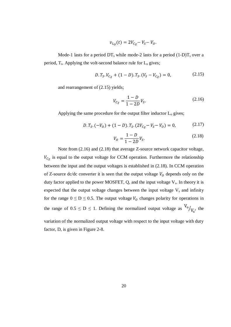
.
Mode-1 lasts for a period DTs while mode-2 lasts for a period (1-D)Ts over a
period, Ts. Applying the volt-second balance rule for Lz gives;
, (2.15)
and rearrangement of (2.15) yields;
(2.16)
Applying the same procedure for the output filter inductor Lo gives;
(2.17)
(2.18)
Note from (2.16) and (2.18) that average Z-source network capacitor voltage,
is equal to the output voltage for CCM operation. Furthermore the relationship
between the input and the output voltages is established in (2.18). In CCM operation
of Z-source dc/dc converter it is seen that the output voltage depends only on the
duty factor applied to the power MOSFET, Q, and the input voltage Vs. In theory it is
expected that the output voltage changes between the input voltage Vs and infinity
for the range 0 ≤ D ≤ 0.5. The output voltage changes polarity for operations in
the range of 0.5 ≤ D ≤ 1. Defining the normalized output voltage as
, the
variation of the normalized output voltage with respect to the input voltage with duty
factor, D, is given in Figure 2-8.

21
Figure 2-8 Variation of the normalized output voltage
with duty factor, D
2.3.2 Dynamic Model in CCM Operation
In this part the steady-state and dynamic model of the converter is obtained.
The dynamic model of a converter is used to estimate the transient response of a
converter against disturbances that the converter is exposed to. The state space
averaging method is widely used in power electronics in order to obtain the dynamic
model of the converter. State-space averaging method is rewriting the differential
equations of the converter in canonical form. It is always possible to obtain a small-
signal averaged model as long as the state equation of the converter is written [16].
For the sake of completeness a brief description of state-space averaging method is
given in this section.
2.3.2.1 State-Space Averaging Method (SSAM)
In SSAM the state variables of the converter are expressed as linear
combinations of state variables and input of the system. The aim of the method is to
linearize the power converter around a steady state operating point for small ac

22
signals. The linearization process is graphically described in Figure 2-9 for a general
case.
Figure 2-9 Linearization of non-linear function at an operating point
The state variables of a system are usually selected as the electrical variables
associated with energy storing elements which are the voltages on capacitors and
currents through inductors for a converter [16]. The state space equations obtained
when the switch is closed, are different than the ones obtained when the switch is
open. In state space averaging method, SSAM the state space equations obtained for
different modes of the converter operation are averaged over the switching period,
Ts. The averaging process removes the switching ripples; however, the ripples at
frequencies higher than the switching frequency must still be represented in the
model. That is, SSAM behaves like a low pass filter in obtaining the dynamic model
of the system. In other words, only the low frequency response of the system can be
estimated using the obtained model. The model response obtained using SSAM
deviates substantially from the actual converter response with the increasing
frequency [1], [16], [18].
The state equations of a converter can be written as;
(2.19)
D
Vo
Non-linear
Characteristic
Linearized Model
Operation-point
23
Here is the state vector. The capacitor voltages and inductor currents in a
converter are elements of . is the input vector which consists of
independent inputs applied to the converter. In general, is the output vector, and
any signal in the converter can be selected as an output signal. It is usually desired to
select the input current to the converter as an output signal [16]. The , , and
are the matrices of proportionality constants which depend on the sizes of the
capacitance, inductance and resistance in the converter.
In order to obtain the small-signal ac model and the steady state dc model it is
necessary to introduce small ac perturbations imposed upon dc steady state
quantities. Introducing such small ac perturbations into the state equations of (2.19)
the state vector and output vector are to be redefined as;
(2.20)
and consider such perturbation on the duty-ratio as well
.
The capital letters show steady-state operating points and the quantities with
show the small ac perturbations subjected to the system around the steady state
operating point.
It is now necessary to obtain the state-space equations in the first subinterval,
mode-1 and in the second subinterval mode-2. In the first subinterval mode-1 shown
in Figure 2-4, it is possible to represent the converter as a linear circuit with the
following state-space equations:
(2.21)
In the second subinterval mode-2 the converter reduces to another linear
circuit having state equations as in (2.22).

24
(2.22)
Averaging the equation sets given in (2.21) and (2.22) over a switching
period, Ts yields;
(2.23)
Small ac perturbation must be introduced to state, input and output vectors
and the duty factor in (2.23) so as to obtain the dynamic model of the converter. For
this purpose (2.20) and (2.23) must be combined. For the sake of simplicity, time
dependency in the notations given in (2.23) will be ignored at the rest of the analysis.
In other words, and will be taken as and for the rest of
the analysis. Combining (2.20) and (2.23) yields;
(2.24)
Reorganizing the terms given in (2.24) and taking into account that the
differentiation of steady-state equilibrium quantities yields zero, the equality stated in
(2.25) is obtained.
(2.25)
)

25
In [16] it is stated that the state-space averaged dc model describing the
converter in steady state is as in (2.26) provided that the frequency of the input
variations for the converter are much lower than the switching frequency.
(2.26)
The averaged matrices in (2.26) are as follows:
(2.27)
In [16] the vectors in (2.26) and (2.27) are defined as the following:
: Steady-state (dc) state vector,
: Steady-state (dc) output vector,
: Steady-state (dc) input vector,
: Steady-state (dc) duty factor.
The solution for (2.26) yields the steady state (dc) state and output vectors as;
(2.28)
.
From (2.25) and (2.26), it is straightforward to define the small signal ac
model state equations;
(2.29)

26
The averaged steady-state dc and small signal ac model state equation are
derived so far. The transfer functions of the system are found by applying Laplace
transformation to the small signal ac model [16]. In order to determine the transfer
functions, the proportionality constant matrices need to be found. This requires
writing the state equations in mode-1 and mode-2. As mentioned earlier the state
space variables are selected as capacitor voltages and inductor currents which
are ,
, and
for Z-source dc/dc converter. The input
voltage, , is chosen as the input vector while the input current, , is chosen
as output vector.
2.3.2.2 State Space Equations of the Converter in CCM
State-Space Equations in Mode-1
Z-source dc/dc converter is as shown in Figure 2-4 during mode-1 in CCM
operation. State-space equations given in (2.30) are valid during mode-1 in CCM
operation.
(2.30)
Reorganizing the equation set in (2.30) in matrix form such as;
27
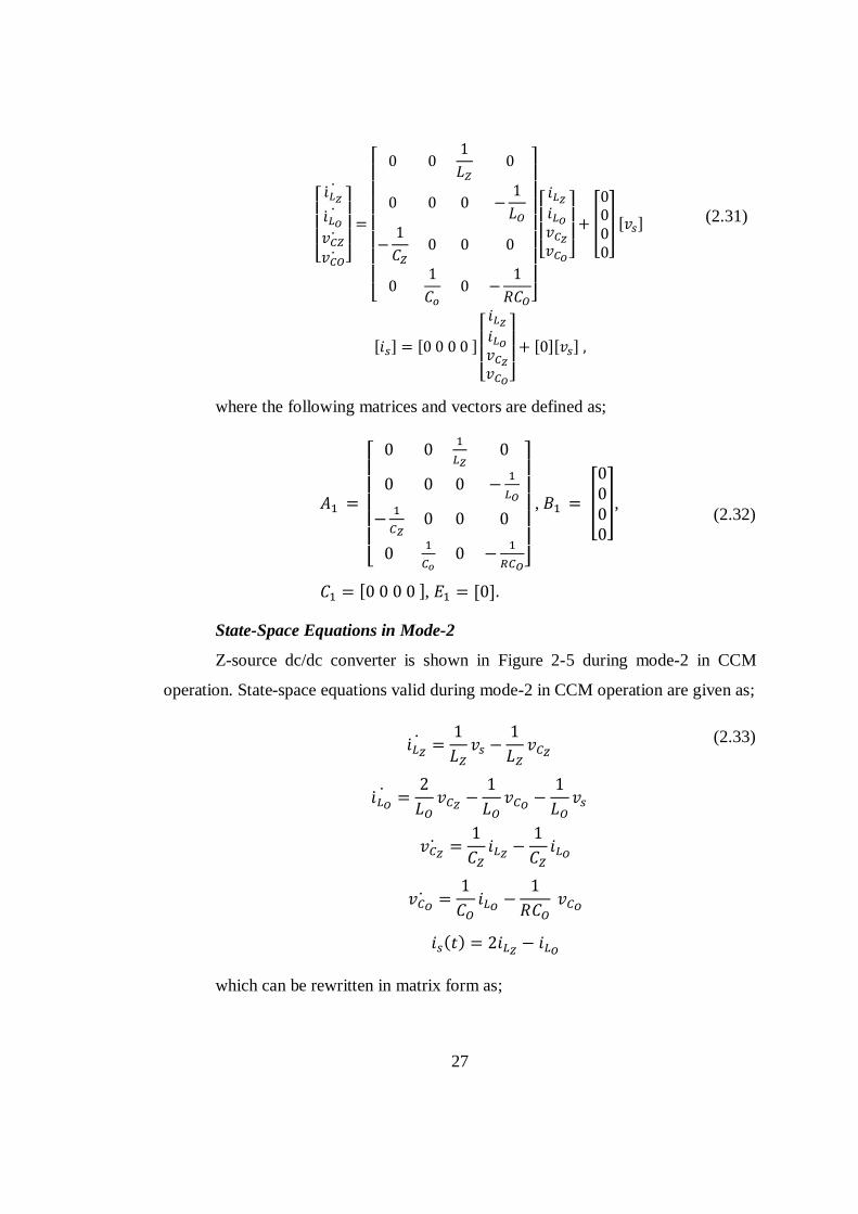
(2.31)
where the following matrices and vectors are defined as;
,
,
,
(2.32)
State-Space Equations in Mode-2
Z-source dc/dc converter is shown in Figure 2-5 during mode-2 in CCM
operation. State-space equations valid during mode-2 in CCM operation are given as;
(2.33)
which can be rewritten in matrix form as;
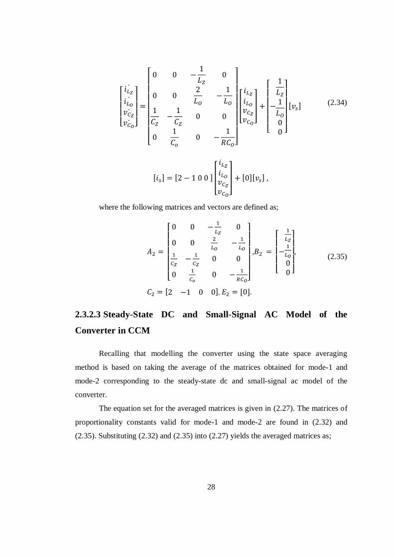
28
(2.34)
where the following matrices and vectors are defined as;
,
,
,
(2.35)
2.3.2.3 Steady-State DC and Small-Signal AC Model of the
Converter in CCM
Recalling that modelling the converter using the state space averaging
method is based on taking the average of the matrices obtained for mode-1 and
mode-2 corresponding to the steady-state dc and small-signal ac model of the
converter.
The equation set for the averaged matrices is given in (2.27). The matrices of
proportionality constants valid for mode-1 and mode-2 are found in (2.32) and
(2.35). Substituting (2.32) and (2.35) into (2.27) yields the averaged matrices as;

29
(2.36)
After obtaining the averaged matrices the steady-state dc and small-signal ac
models of the converter can be obtained.
Steady-State DC Model
The solution for the state and output vectors in steady-state is given in (2.28).
By using (2.28) and the averaged matrices given in (2.36) the steady-state dc model
of the converter is obtained as the following:
(2.37)
(2.37) expresses the steady-state dc operating points for the capacitor voltages
and inductor currents. It is understood from (2.37) that the capacitor voltages depend

30
only on the duty-factor and the input voltage in CCM operation. However the
inductor currents depend to the duty factor and the input voltage but additionally also
on the load resistance.
At this point it is also important to notice that the capacitor voltages are equal
to each other according to the steady-state dc model obtained. The relationship
between the input voltage and the Z-source network capacitor voltage and output
filter capacitor voltage were found in (2.16) and (2.18). A close investigation of
(2.37) reveals the fact that exactly the same relationship between the input voltage
and capacitor voltages is obtained by the SSAM. This is strong evidence that the
steady-state dc model obtained by SSAM is valid and complies with the previous
results obtained in 2.3.1.
Small-Signal AC Model and Determination of the Transfer Functions
The small-signal ac model of the converter is stated in (2.29). Rewriting
(2.29) by substituting the matrices of proportionality constants found in (2.32) and
(2.35) into (2.29), the small-signal ac model of the Z-source dc/dc converter is
obtained as follows:
(2.38)
where ,
, and
show the steady-state dc operating points of the
capacitor voltages and inductor currents. On the other hand, ,
, and
are the small ac perturbations around the steady-state operating point of the
capacitor voltages and inductor currents.

31
Expressing the state-space equation set for the small-signal ac model given in
(2.38) separately makes the analysis much more understandable. Hence writing the
equations separately rather than the matrix form and substituting the averaged
matrices found in (2.36) to (2.38), the following equation set is obtained.
(2.39)
In determining the transfer functions of the converter “Laplace Transform” of
the equations given in (2.39) must be found. Thus, the “Laplace Transform” of (2.39)
yields;
(2.40)
.
Considering the controller design of the Z-source dc/dc converter it is
assumed that the dynamic change in the output voltage, depends on the input
voltage and duty factor applied to the switching power MOSFETs. As a result it is

32
possible to express the output voltage variation in terms of input voltage variation
and duty-factor variation as shown in (2.41).
(2.41)
The definitions for the variables and transfer functions stated in (2.41) are as
follows:
“Laplace Transform” of the small ac perturbation around the output voltage,
“Laplace Transform” of the small ac perturbation around the input voltage,
“Laplace Transform” of the small ac perturbation around the duty factor,
Duty-factor, to output voltage, transfer function
Input voltage, to output voltage, transfer function
In order to determine the duty-factor to output voltage transfer function it is
wise to assume that there is no small ac perturbation around the input voltage. That is
it is purely dc. As a result the Laplace Transform of the small ac perturbation around
the input voltage, is zero. In this case the duty-factor, to output voltage,
transfer function is expressed as in;
(2.42)
where the coefficients given in (2.42) are

33
.
In the same manner setting to zero the input voltage, to output
voltage transfer function can be found as;
(2.43)
Note that the denominator of (2.43) is exactly the same of the one obtained in
(2.42). The coefficients of the numerator of the transfer function given in (2.43) are
as follows.
It is also necessary to obtain the duty factor to inductor current transfer
function which will be utilized in the controller design part.
(2.44)
with the coefficients as follows;

34
The results obtained in (2.42)-(2.44) reveal that the denominator of the two
transfer functions are exactly the same. This completes the mathematical analysis of
Z-source dc/dc converter in CCM operation.
2.3.3 Mathematical Analysis of Simplified Model in DCM-2
There are three different possibilities for discontinuous conduction mode
(DCM) operation of Z-source dc/dc converter as mentioned in [14].
DCM-1: In this mode the input current flowing through the input diode
shown in Figure 2-2 falls to zero before the beginning of the next period. On the
other hand, the current flowing through does not fall to zero before the beginning
of the next period.
DCM-2: In this mode the input current flowing through the input diode
shown in Figure 2-2 does not fall to zero before the beginning of the next period. On
the other hand the current flowing through falls to zero before the beginning of
the next period.
DCM-3: Both of the currents flowing through the input diode and the
rectification diode shown in Figure 2-2 fall to zero before the beginning of the
next period.
The analysis of the Z-source dc/dc converter has been done in DCM-1
previously and reported in the literature [14]. In this work the mathematical analysis
of the converter in DCM-2 operation is done and the small-signal ac model of the
converter in DCM-2 is obtained.
There are three different modes over one switching period during the DCM-2
operation of the Z-source dc/dc converter.
MODE-1
i. It starts when Q starts to conduct. It lasts for a time interval t1, which is
shown in Figure 2-13 and Figure 2-14.
ii. The Z-source network inductors, Lz, are energized by the Z-source
network capacitors, Cz.

35
iii. The loop equations valid for mode-1 in DCM-2 operation are shown in
Figure 2-10.
iv. Applying the Kirchhoff’s voltage law around LOOP-2 shown in Figure
2-10, the voltage across the Z-source network inductor, , during t1 interval is
found as;
(2.45)
v. During mode-1 the input diode is reverse biased so that the current
drawn from the supply is zero.
vi. Since the current drawn from the supply is zero the output filter capacitor
Co and inductor Lo supply the necessary energy to the load. Since the energy required
by the load is given by the path of Lo, the rectification diode Dr is conducting during
mode-1 in DCM-2 operation.
vii. Applying the Kirchhoff’s voltage law around LOOP-3 shown in Figure
2-10, the voltage across the output filter inductor voltage, , is equal to the
opposite of the output voltage .
(2.46)
viii. Applying the Kirchhoff’s current rule at “Node A”, the Z-source network
capacitor current, is found to be equal to the opposite of the Z-source network
inductor current, .
(2.47)
ix. Finally applying the Kirchhoff’s current rule at “Node B”, the output filter
capacitor current, is found to be as;
(2.48)

36
Figure 2-10 Active loops during mode-1 in DCM-2 operation of Z-source dc/dc
converter
MODE-2
i. It starts when the rectification diode current falls to zero and Dr stops to
conduct. It lasts for time interval t2.
ii. The Z-source capacitors continue to energize the Z-source inductors
during mode-2.
iii. The loop equations valid during mode-2 in DCM-2 operation are shown in
Figure 2-11.
iv. Applying the Kirchhoff’s voltage law around LOOP-2 shown in Figure
2-11, the voltage across the Z-source network inductor, , during t2 time
interval is found as ;
(2.49)
v. During mode-2 the input diode is still reverse biased so that the current
drawn from the supply is still zero.
vi. Since the rectification diode stops to conduct, the current flowing
through the output filter is zero. This means that the load is energized only by the
output filter capacitor during mode-2.
vii. Since current is constant and zero during mode-2 no voltage will be
induced on according to the Faraday’s Law for t2 period.
VS
Di
CZ CZ
LZ
LZ
Q
LO
CO RL
+
vo
-
Dris(t)=iDi(t) + vDi(t) -
iCz(t)
+
vCz(t)
-
iCz(t)
+
vCz(t)
-
+ vLz(t) -
iLz(t)
iQ(t)
+
vQ(t)
-
+ vDr(t) -
iDr(t)=iLo(t)
+ vLo(t) -
+
vCo(t)
-
iCo(t) io(t)
iLz(t)
LOOP-1
- vLz(t) +
LOOP-2 LOOP-3
Node A Node B
37
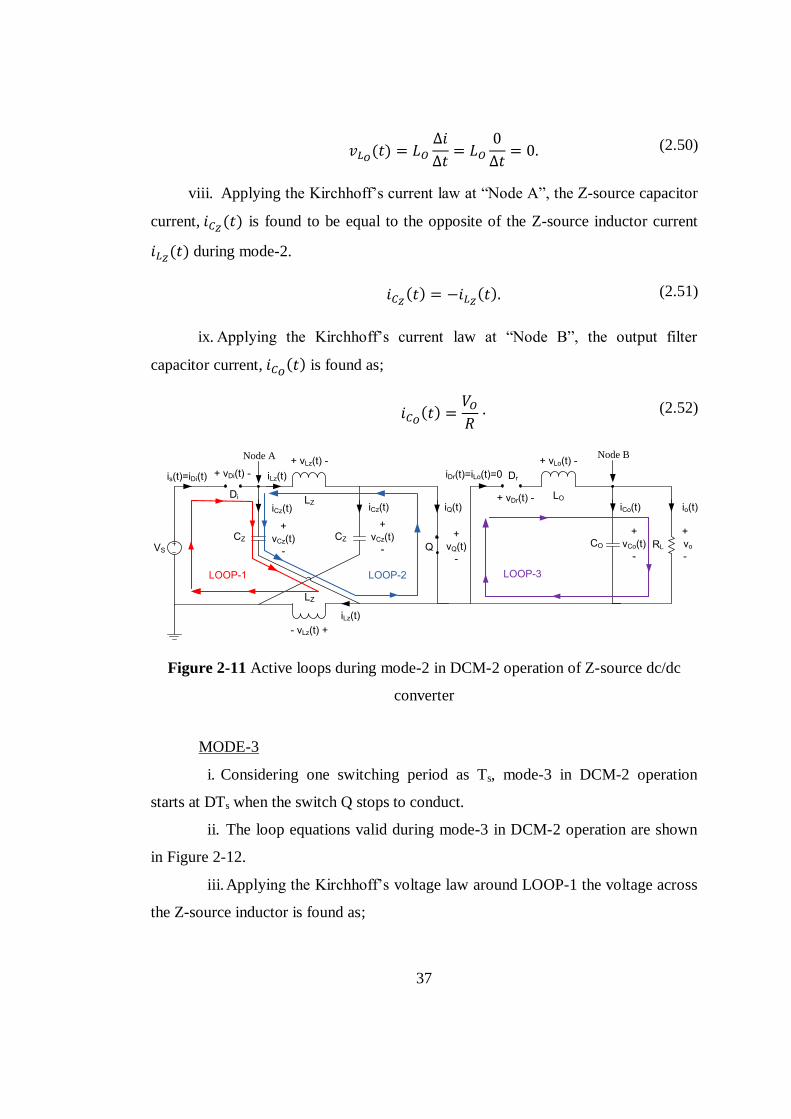
(2.50)
viii. Applying the Kirchhoff’s current law at “Node A”, the Z-source capacitor
current, is found to be equal to the opposite of the Z-source inductor current
during mode-2.
(2.51)
ix. Applying the Kirchhoff’s current law at “Node B”, the output filter
capacitor current, is found as;
(2.52)
Figure 2-11 Active loops during mode-2 in DCM-2 operation of Z-source dc/dc
converter
MODE-3
i. Considering one switching period as Ts, mode-3 in DCM-2 operation
starts at DTs when the switch Q stops to conduct.
ii. The loop equations valid during mode-3 in DCM-2 operation are shown
in Figure 2-12.
iii. Applying the Kirchhoff’s voltage law around LOOP-1 the voltage across
the Z-source inductor is found as;
VS
Di
CZ CZ
LZ
LZ
Q
LO
CO RL
+
vo
-
Dris(t)=iDi(t) + vDi(t) -
iCz(t)
+
vCz(t)
-
iCz(t)
+
vCz(t)
-
+ vLz(t) -
iLz(t)
iQ(t)
+
vQ(t)
-
+ vDr(t) -
iDr(t)=iLo(t)=0
+ vLo(t) -
+
vCo(t)
-
iCo(t) io(t)
iLz(t)
LOOP-1
- vLz(t) +
LOOP-2 LOOP-3
Node A Node B

38
(2.53)
iv. Applying the Kirchhoff’s voltage law around LOOP-1 the voltage across
the output filter inductor can be written as;
(2.54)
v. The current flowing through forces the input diode to conduct during
mode-3 in DCM-2 operation.
vi. Applying the Kirchhoff’s current law at “Node A” yields that the Z-
source capacitor current is equal to the difference between the current drawn from
the supply, and the Z-source inductor current, ;
(2.55)
vii. Applying the Kirchhoff’s current law at “Node B” it is seen that (2.56)
is valid during mode-3.
(2.56)
viii. Applying the Kirchhoff’s current law at “Node C” the Z-source
capacitor current can be expressed as given in (2.57) during mode-3.
(2.57)
Combining (2.55) and (2.57) it is possible to obtain (2.58).
(2.58)

39
Figure 2-12 Active loops during mode-3 in DCM-2 operation of Z-source dc/dc
converter
In order to continue the mathematical analysis in DCM-2 operation it is
necessary to stick to the assumptions stated in (2.10). With these assumptions the
voltage and current waveforms of Z-source dc/dc converter in DCM-2 operation are
given in Figure 2-13 and Figure 2-14.
VS
Di
CZ CZ
LZ
LZ
Q
LO
CO RL
+
vo
-
Dris(t)=iDi(t)+ vDi(t) -
iCz(t)
+
vCz(t)
-
iCz(t)
+
vCz(t)
-
+ vLz(t) -
iLz(t)
iQ(t)
+
vQ(t)
-
+ vDr(t) -
iDr(t)=iLo(t)
+ vLo(t) -
+
vCo(t)
-
iCo(t) io(t)
iLz(t)
LOOP-1
- vLz(t) +
LOOP-2
Node A Node BNode C

40
DTs Ts
t
Duty-Factor
t
ILz(t)
t
VLz(t)
t
ILo(t)=IDr(t)
t
VLo(t)
ILz(max)
ILz(min)
ILo(max)
VCz(t)
VS(t)-VCz(t)
-VO(t)
2VCz(t)-VS(t)-VO(t)
MO
DE
-1
MO
DE
-3
t1 t3
t
VCz(t)
t
ICz(t)
t
VCo(t)
t
ICo(t)
ILz(avg)
ILo(avg)
ΔVCz
ΔVCo
VCz
-ILz(min)
-ILz(max)
ILz(max)
ILz(min)-ILo(max)
ILo(max)-ILo(avg)
-ILo(avg)
MO
DE
-2
t2
DTs Ts
t
Duty-Factor
MO
DE
-1
MO
DE
-3
t1 t3
MO
DE
-2
t2
d1Ts d1Ts
Figure 2-13 Capacitors ( and
) and inductors ( and
) voltage and current
waveforms during the DCM-2 operation of Z-source dc/dc converter

41
DTs Ts
t
Duty-Factor
MO
DE
-1
MO
DE
-3
t1 t3
MO
DE
-2
t2
t
IDi(t)
t
VDi(t)
VS(t)-2VCz(t)
2ILz(max)
2ILz(min)-ILo(max)
DTs Ts
t
Duty-Factor
MO
DE
-1
MO
DE
-3
t1 t3
MO
DE
-2
t2
t
IQ(t)
t
VQ(t)
2VCz(t)-VS(t)
2ILz(min)-ILo(max)
2ILz(max)
t
VDr(t)
-VO(t)
d1Ts d1Ts
Figure 2-14 Switching elements (Di and Q) voltage and current waveforms during
the CCM operation of Z-source dc/dc converter
In order to determine the input-output voltage relationship, the same
procedure applied in the mathematical analysis in CCM operation in 2.3.1 is
followed. Within this scope it is required to apply the volt-second balance rule to the
two inductors in Z-source dc/dc converter.
The voltages across the inductors during mode-1 in DCM-2 operation are as
follows:
(2.59)
The voltages across the inductors during mode-2 in DCM-2 operation are as
follows.
(2.60)

42
Finally the voltages across the inductors during mode-3 in DCM-2 operation
are as follows:
(2.61)
After the determination of the inductor voltages during the operating modes
of DCM-2 operation, it is now necessary to apply the volt second rule to the
inductors in the converter. Applying volt-second balance rule for Lz over a period
yields
(2.62)
It is possible to obtain the relationship between the input voltage and the Z-
source capacitor voltage from (2.62).
(2.63)
Writing the volt-second balance equation for Lo inductor gives;
(2.64)
The relationship between the input voltage and the output voltage can be
constructed using (2.63) and (2.64).
(2.65)
can be determined from (2.65) as follows:
(2.66)
In order to determine the relationship between the input voltage and output
voltage must be written in terms of the circuit parameters, Lz, Lo, R, D, Ts. In

43
order to achieve this goal the current changes in the inductors are needed to be
written using the volt-second balance rule. With careful examination of Lz current
change in mode-1 and mode-2 shown in Figure 2-13, it is possible to derive;
(2.67)
Similarly the current change in Lo during mode-1 can be expressed as;
(2.68)
Determining the equality for the inductor current changes in mode-3 yields;
(2.69)
Finally, it is also necessary to express the average current drawn from the
supply. It is clear from Figure 2-3 that the current drawn from the supply is equal to
the current flowing through the input diode Di. Hence referring to Figure 2-14 the
average current drawn from the supply can be expressed from as;
(2.70)
The dual of volt second balance rule for the inductors is the current second
balance rule for the capacitors. In dc/dc converter analysis it is sometimes necessary
to apply the current-second balance rule for the capacitors in order to determine the
input and output voltage relationship. The current-second rule dictates that the
current-second area under the capacitor current variation over one switching period is
zero. In other words, the average current of a capacitor is zero over a period. In order
to apply the current-second balance rule to the capacitors of the converter it is first
necessary to determine the average currents flowing through them in each mode

44
during the DCM-2 operation. At this point a new notation for the average current in
each mode of operation is needed to be introduced.
represents the average of the current
for the time duration
.
Next step is applying the current-second balance rule to the Z-source
capacitor as;
(2.71)
Reorganizing the terms given in (2.71) it is possible to obtain;
(2.72)
The average current drawn from the supply is determined in (2.70). It is
possible to express the average current drawn from the supply, in terms of only
the Lo inductor current by combining (2.70) and (2.72).
(2.73)
So far the average current drawn from the supply is determined. In order to
find the input and output voltage relationship it is now necessary to use the principle
of conservation of power. Assuming that all the components in Z-source dc/dc
converter are lossless, then the power taken from the supply is equal to the power
given to the load,
(2.74)
where R represents the load resistance. Recalling that given in
(2.68), from (2.70) and (2.74) one obtains;

45
(2.75)
Equation (2.75) can be rewritten as;
(2.76)
Reorganizing (2.65), one obtains;
(2.77)
Inspection of (2.76) and (2.77) reveals that the left hand sides of the equalities
are the same. Hence, the right hand sides of the equalities must also be the same, to
give;
(2.78)
The solution for (2.78) yields;
(2.79)
With the results obtained in (2.79), the relationship between input and output
voltage can be stated as;
(2.80)
where
(2.81)

46
Critical Load for DCM-2 Operation
The condition for the transition between CCM and DCM-2 operation is
worthy to note as well. Referring to Figure 2-13, one notes that in DCM-2 operation
must hold. The critical load which will cause the converter to operate at the
instant of transition from CCM to DCM-2, the duty factor D is needed to be equal to
.
(2.82)
The solution for (2.82) gives the critical load as;
(2.83)
In conclusion if is satisfied, then the Z-source converter transits
from CCM operation into the DCM-2 operation.
2.3.4 Obtaining Dynamic Model in DCM-2
In this part the dynamic model of the converter in DCM-2 operation is
obtained using the circuit averaging method. Circuit averaging method is another
well-known method for derivation of the converter model. In SSAM the state
equations of the converter are averaged. However, in circuit averaging method the
converter waveforms are averaged directly [16].For the sake of completeness of the
analysis in DCM-2 operation a brief description of circuit averaging method is given
in this section.
2.3.4.1 Circuit Averaging Method (CAM)
CAM involves averaging and small signal linearization which makes it
equivalent to state space averaging method, SSAM. The key point in CAM is to
replace the converter switches, diodes and MOSFET’s in the converter structure,

47
with dependent or independent voltage and current sources. In this manner a time
invariant circuit is obtained. The next step is averaging the converter waveforms over
a switching period.
The main idea of circuit averaging method, CAM is to find an averaged
circuit model for the switch network. The resulting averaged circuit model can then
be inserted into the converter circuit in order to obtain an averaged circuit model.
The first step in CAM is to obtain a time-invariant circuit. Next is averaging the
waveforms. As a final step perturbation and linearization is needed in order to obtain
the dynamic model of the converter.
2.3.4.2 Time-Invariant Circuit in DCM-2
The first step in the circuit averaging method, CAM is to replace the switch
network in the converter with voltage and current sources such that the circuit
connection does not change in time. Throughout this process the assumptions stated
in (2.10) are still valid.
As seen from Figure 2-3, in the simplified model of Z-source dc/dc converter
there are three switching elements, Di, Dr and Q. The averaged values of the voltage
and current waveforms of these elements are needed to be determined in terms of the
converter state variables (inductor current and capacitor voltages) and the converter
independent inputs (input voltage and duty cycle) in order to obtain a time-invariant
circuit with CAM.
The Input Diode, Di, Voltage Waveform Averaging
Throughout the analysis the voltage waveform of the input diode is as shown
as as Figure 2-15.

48
Figure 2-15 Input diode voltage and current waveforms over a period
As illustrated in Figure 2-15 the voltage change on Di can be expressed as;
Mode-1
(2.84)
Mode-2
Mode-3
where and
stand for the input voltage and the Z-source
capacitor voltages averaged over a period respectively. Taking the average of the
input diode voltage waveform over a switching period yields;
. (2.85)
MOSFET, Q, Voltage Waveform Averaging
Throughout the analysis the voltage waveform of the switch (MOSFET) is
typically as . The voltage and current waveforms of Q are shown in Figure
2-16.
DTs Ts
t
Duty-Factor
MO
DE
-1
MO
DE
-3
t1 t3
MO
DE
-2
t2
t
IDi(t)
t
VDi(t)
VS(t)-2VCz(t)
2ILz(max)
2ILz(min)-ILo(max)
d1Ts

49
Figure 2-16 Switch (MOSFET) waveforms over a period
As illustrated in Figure 2-16 the voltage change on the switch MOSFET, Q,
can be expressed as in (2.86).
Mode-1 (2.86)
Mode-2
Mode-3
Taking (2.86) into consideration the average switch voltage over a switching
period is as;
(2.87)
The Rectification Diode, Dr, Voltage Waveform Averaging
Throughout the analysis the voltage waveform on the rectification diode is
typically shown in Figure 2-17.
DTs Ts
t
Duty-Factor
MO
DE
-1
MO
DE
-3
t1 t3
MO
DE
-2
t2
t
IQ(t)
t
VQ(t)
2VCz(t)-VS(t)
2ILz(min)-ILo(max)
2ILz(max)
d1Ts

50
Figure 2-17 Rectification diode waveforms over a period
Referring to Figure 2-17 the voltage change on Dr can be expressed as;
Mode-1 (2.88)
Mode -2
Mode -3
Taking the average of the rectification diode voltage waveform over a
switching period yields;
(2.89)
It is now necessary to determine the average value for the current waveforms
of the diodes and switch over a switching period, Ts.
The Input Diode, Di, Current Waveform Averaging
The current waveform of the input diode is shown in Figure 2-15 and its
variation is given as;
t
VDr(t)
-VO(t)
t
IDr(t)
ILo(max)
DTs Ts
t
Duty-Factor
MO
DE
-1
MO
DE
-3
t1 t3
MO
DE
-2
t2
d1Ts

51
Mode-1 (2.90)
Mode-2
Mode-3
In order to determine the average current time integral of the current
waveform over a switching period must be determined as;
(2.91)
where represents the area under the current waveform over one
period. This can be calculated as;
(2.92)
For finding the circuit average model of the input diode, it is necessary to
express the current waveform in terms of
, ,
and
duty factor, . The expression
in (2.92) must
be rewritten for this purpose. Using the expression (2.72), the expression (2.92) can
be put in the form;
(2.93)
As a final step, using (2.69) and (2.93) the following equation is obtained as;
(2.94)
Considering the assumptions stated in (2.10), the average voltages on the
capacitors in the converter and the input voltage to the converter can be expressed as;

52
(2.95)
Combining (2.94) and (2.95) one obtains;
(2.96)
In (2.91) the average value of the input diode current is found in term of .
Using this equality, the average value of the input diode current can be expressed as
follows;
(2.97)
Finally by (2.85), (2.89) and (2.97) the average value of the input diode
current can be expressed as;
(2.98)
Switch, Q, Current Waveform Averaging
The current waveform of the switch is typically as shown in Figure 2-16 with
variation in time as;
Mode-1
(2.99)
Mode-2
Mode-3
The same procedure followed in determination of the average current
waveform of the input diode is followed in order to determine the average current
waveform of the switch. Hence, as a first step the average current waveform of the
switch is defined as;

53
(2.100)
where represents the area under the current waveform over one
period. The area under current waveform can be calculated as;
(2.101)
Substituting (2.72) into (2.101) yields;
(2.102)
Substituting found in (2.69) into (2.102) gives;
(2.103)
Under the assumptions stated in (2.95) it is possible to rewrite (2.103) as;
(2.104)
The average current waveform of the switch can be expressed as;
(2.105)
From (2.87), (2.89) and (2.105) one obtains;

54
(2.106)
The Rectification Diode, Dr, Current Waveform Averaging
The current waveform of the rectification diode is typically as shown in
Figure 2-17 with its variation being;
Mode-1 (2.107)
Mode-2
Mode-3
The average value of the current waveform of the rectification diode is
defined as;
(2.108)
where is the area under the current waveform shown in Figure 2-17.
It is possible to express as;
. (2.109)
Substituting (2.68) for into (2.109) yields;
(2.110)
Replacing the output voltage in terms of the average voltage of the
rectification diode over one period found in (2.89) results as;
(2.111)

55
Finally, it is straightforward to find the average current of the rectification
diode over a period as;
(2.112)
In the analysis of Z-source dc/dc converter in DCM-2 mode of operation the
average voltage and the current waveforms of the switching elements are found so
far. It is now time to determine the small signal ac model of the converter at a fixed
operating point (V1, V2, V3 and D). For this purpose it is required to add small ac
perturbations ( , , ) to the fixed operating points. Adding small
ac perturbations to the average voltage and current waveforms and the duty factor of
the converter at the selected fixed operating points yield the followings;
(2.113)
In (2.113) the capital letters stand for the dc operating points while small
letters with on top represents the small ac perturbations. In the circuit averaging
method, CAM the small ac perturbations are defined as;
(2.114)

56
where the coefficients can be found by using the Taylor series expansion [16].
Considering (2.98) it is understood that the average current of the input
diode, can be expressed as a function of
;
(2.115)
Applying the Taylor expansion to (2.115) around the operating point
yields the expressions;
(2.116)
Equating the corresponding terms in both sides of (2.116) to have;
Combining (2.114) and (2.116), the coefficients for the ac perturbation valid
for can be determined as;
(2.117)

57
The same procedure can be followed for and
.Therefore
expressing as;
(2.118)
and applying the Taylor expansion to (2.118) around the operating point
yields the expression given below;
(2.119)
Equating the corresponding terms in both sides of (2.119) to have;
Combining (2.114) and (2.119), the coefficients for the ac perturbation valid
for can be determined as;
(2.120)

58
Repeating the procedure for ;
(2.121)
Applying the Taylor expansion to (2.121) around the operating point
yields the expression;
(2.122)
.
Equating again the corresponding terms in both sides of (2.122) to have;
Combining (2.114) and (2.122), the coefficients for the ac perturbation for
can be determined as;
(2.123)
In order to determine the small signal ac model of the converter in DCM-2
operation the partial derivatives in (2.117), (2.120) and (2.123) should be
determined. MATLAB is quite suitable for this complex and long task. These partial
derivatives obtained this way are given in Appendix A.

59
2.3.4.3 Small-Signal AC Model of the Converter in DCM-2
After determination of the coefficients for DCM-2 operation, the next step is
to establish the small signal ac model of the converter. With the coefficients found in
2.3.4.2 the small signal ac models for the input diode, switch and the rectification
diode can be obtained as shown in Figure 2-18, Figure 2-19 and Figure 2-20.
Figure 2-18 Small signal ac model of the input diode
Figure 2-19 Small signal ac model of the switch
Figure 2-20 Small signal ac model of the rectification diode
These small signal ac models are inserted to the converter so that small signal
ac model of the total converter in DCM-2 operation is obtained as shown in Figure
2-21.
j1d(t)~ g1v3(t)~ r1v1(t)
+
-
i1(t)
~
~
j2d(t)~ g2v3(t)~ r2v2(t)
+
-
i2(t)
~
~
j3d(t)~ r3v3(t)
+
-
i3(t)
~
~

60
Figure 2-21 Small signal ac model of the Z-source dc/dc converter in DCM-2
operation
So far in section 2.3.4, the mathematical analysis of the Z-source converter in
DCM-2 operation is conducted and the small signal ac model of the converter is
obtained. The transfer function analysis of the converter in CCM operation reveals
the duty factor-to-output voltage transfer function can be determined by setting the
small signal perturbation in input voltage, , to zero [16].
For determination of the transfer functions in DCM-2, another assumption is
necessary. Recalling that, the small signal ac models of the converters are used to
estimate the low frequency (frequencies far below the switching frequency) response
of the converters. In [16] it is mentioned that the poles due to the inductor in a
converter in DCM operation are located relatively at high frequencies. So, it is
assumed that the poles due to the Z-source network inductor, and the output filter
inductor are at high frequencies so that their effects on the transfer function can be
neglected so that the order of the real transfer function will be lowered. Yet the
transfer function obtained will still provide a good estimation for the low frequency
response of the converter. Under these circumstances the small signal ac model of
the Z-source converter in DCM-2 operation will be as follows.
j1d(t)~
r1
i1(t)~
+
-vS(t)~
g1v3(t)~
j2d(t)~r2g2v3(t)~
j1d(t)~
r3
RCO
LOLZ
LZ
CZ CZv2(t)
+
-
~
i2(t)~
i3(t)~
v1(t)+ -~
v3(t)+ -~
vO(t)
+
-
~

61
Figure 2-22 Reduced order small signal ac model of the Z-source dc/dc converter
Duty Factor to Output Voltage Transfer Function,
So far the mathematical analysis of Z-source dc/dc converter is done for
DCM-2 operation and the reduced order small signal ac model is obtained. The next
step is to determine the duty factor to output voltage transfer function. For this
purpose the perturbation in the input voltage must be set zero so that the output
voltage perturbation will be only due to the perturbation in the control input, duty
factor. The small signal ac model to be used in order to determine the will
be as the following.
Figure 2-23 Small signal ac model for determination of in DCM-2
operation
j1d(t)~
r1
i1(t)~
g1v3(t)~
j2d(t)~ r2g2v3(t)~
j1d(t)~
r3
RCO
CZ CZv2(t)
+
-
~
i2(t)~
i3(t)~
v1(t)+ -~
v3(t)+ -~
vO(t)
+
-
~
A
+
-vS(t)~
j1d(t)~r1
i1(t)~
g1v3(t)~j2d(t)~ r2g2v3(t)~
j1d(t)~
r3
RCO
CZ CZv2(t)
+
-
~
i2(t)~
i3(t)~
v1(t)
+
-~
v3(t)+ -~
vO(t)
+
-
~
A B

62
Referring to Figure 2-23 the following equalities can be determined.
(2.124)
Moreover applying the Kirchhoff’s current low at node A yields;
(2.125)
Finally applying the Kirchhoff’s current low at node B, one obtains the output
voltage as;
(2.126)
Using equations given in (2.124)-(2.126) the duty factor to output voltage
transfer function in DCM-2 operation can be expressed as;
(2.127)
where
(2.128)
Input Voltage to Output Voltage Transfer Function,
In order to determine the input voltage to output voltage transfer function the
perturbation in the duty factor, , must be set zero so that the output voltage

63
variation will only be due to the variation in the input voltage. By setting equal
to zero the reduced small signal ac model of the Z-source dc/dc converter will be as
shown in Figure 2-24.
Figure 2-24 Small signal ac model for determination of
in DCM-2
operation
From Figure 2-24 it is possible to express the following equalities.
(2.129)
As a second step it is necessary to apply the Kirchhoff’s current law at node
A.
(2.130)
Finally the output voltage must be expressed in order to determine the input
voltage to output voltage transfer function. Application of Kirchhoff’s current law at
node B yields;
r1
i1(t)~
+
-vS(t)~
g1v3(t)~
r2g2v3(t)~
r3
RCOCZ CZv2(t)
+
-
~
i2(t)~
i3(t)~
v1(t)+ -~
v3(t)+ -~
vO(t)
+
-
~
A B

64
(2.131)
Using equations (2.129)-(2.131) the input voltage to output voltage transfer
function can be defined as the following.
(2.132)
where and are as defined in (2.128).

65
CHAPTER 3
SIMULATION RESULTS OF Z-SOURCE DC/DC
CONVERTER
3.1 Introduction
In this chapter, the simulation results of the Z-source dc/dc converter are
examined. The first goal of the simulations is to verify the waveforms of the
converter displayed in Figure 2-6, Figure 2-7, Figure 2-13 and Figure 2-14 related to
CCM and DCM-2 operations. The second goal of the simulations is to verify the
validity of the mathematical analysis conducted in Chapter 2. The input-output
voltage relationships found in Chapter 2 are verified via the simulation results.
Besides these goals the validity of the input voltage-to-output voltage and duty
factor-to-output voltage transfer functions in estimating the low frequency response
of the converter determined in Chapter 2 are confirmed by the simulation results
conducted for both CCM and DCM-2 operations of the converter. The circuit level
simulations are carried out by SIMPLORER but verification of the validity of the
transfer functions are made by using SIMULINK.
3.2 Determination of the Sizes of the Energy Storage Components
Before introducing the simulation results, the sizes of the energy storage
components in the converter must be determined. The operating condition of the

66
converter depends crucially on the proper selection of the sizes of the inductors and
capacitors in the converter. The operational specifications for the converter are;
Nominal input voltage,
Output voltage,
Maximum output power, .
Assuming that the load is resistive purely, the load resistance, R at full load
is;
One of the most important parameters of the converter design is to determine
the switching frequency of the converter. The switching frequency of the converter
directly affects the magnitude and size of the energy storage components in a
converter. It is known that higher switching frequency results in smaller size of the
energy storage components. This reduces the dimensions of the converter and
decreases the cost. On the other hand, high switching frequency causes higher
switching loss on the switch. In Z-source full bridge dc/dc converter, there are four
switches, and this sets an upper limit on the switching frequency. A high switching
frequency makes the converter less efficient. Considering these issues the switching
frequency of Z-source dc/dc converter is selected to be 100 kHz.
Next step in the design phase is determination of the sizes of the energy
storage components in the converter. In the selection of the sizes of the energy
storage components the nominal operating duty factor plays an important role. Using
the input-output voltage relationship (2.18) the duty factor of the converter under
nominal operating conditions can be determined as;
(3.1)

67
Considering the nominal input voltage and the desired output voltage the
nominal duty factor is found to be . This duty factor will be used in the
selection of the sizes of inductors and capacitors in the converter later.
Beginning with selection of the sizes of the Z-source network inductors and
output filter inductor, it is important to determine the average current flowing
through them. Under full load operating condition, the maximum average current
flows through the inductors, but that level of the average current must not cause the
cores used for the inductors to saturate. The average current flowing through the Z-
source inductors can be found using the fact that input power, Pin is equal to the
output power, Po for a lossless converter. Since the current carried by the Z-source
capacitors are zero in steady state, in Z-source topology the average current drawn
from the supply flows through the inductors, so that one can write the inductor
current as;
(3.2)
Considering the full-load condition, the maximum value of the average
current, through Lz is 6 A.
Another important issue for the inductor design is determination of the
magnitude of the ripple current through the inductor. The magnitude of the ripple
current of the inductors determines the operating mode of the converter. It is desired
to operate the converter both in CCM and DCM-2 operation within the scope of this
work. Hence the ripple current magnitude is selected to be 40% of the average
current, carried by the Z-source network inductor, Lz. Recalling the expression
for the Z-source inductor voltage, equality valid during mode-1 in CCM
operation we have;
(3.3)
and from which

68
Under nominal operating conditions the input voltage, , of the converter is
30 V. The desired output voltage, , is 60 V. The duty factor is therefore 0.33 for
this operating condition. The switching frequency of the converter is selected as 100
kHz, with . The ripple current magnitude of the Z-source
network inductor is determined as
in order to make sure
that the converter is able to operate both in CCM and DCM-2 operation. Thus, all the
parameters needed to determine the size of the Z-source inductor taking place in
(3.3) are known to give .
The same procedure is followed to determine the size of the output filter
inductor. The average current flowing through the output filter inductor is actually
the load current. Hence the maximum average current, of the output filter inductor
can be found as;
(3.4)
The main objective of this work is to examine the CCM and DCM-2
operations of the converter. In Chapter 2, it has been shown that the output filter
inductor current falls to zero in DCM-2 operation. This means that the ripple current
magnitude of the output filter inductor must be greater than 100% of the average
inductor current; 133% of the average current of the output filter inductor has been
adopted here. Remembering that the output filter inductor voltage, during mode-
1 in CCM operation one obtains;
(3.5)
and from which

69
The output voltage, nominal operating duty factor and switching frequency of
the converter are already known, thus determining the ripple current magnitude of
the output filter inductor as 133% of the average current with
. The output filter inductor is then by
(3.5).
The other energy storage elements in the converter are the Z-source network
and output capacitors. The output voltage ripple is required to be less than 5% of the
output voltage. Moreover the maximum overshoot voltage during the load changes is
desired to be less than 10% of the output voltage. The output filter capacitor
satisfying the requirements is 1 mF. There is no condition imposed on the voltage
ripple magnitude of Z-source network capacitor, but for the control performance
issues it is seemed to be more suitable to select it as 20 µF. Moreover, by this way
the Z-source network capacitor can be constructed with ceramic capacitors which
have excellent dynamic frequency response and the lowest ESR in capacitor family.
As a result the power loss in Z-source capacitors will be very low which will
improve the efficiency of the converter.
Finally, sizes of all the energy storage elements in the converter and the
switching frequency of the converter are determined. The parameters of the converter
used in the simulation are tabulated in Table 3-1.
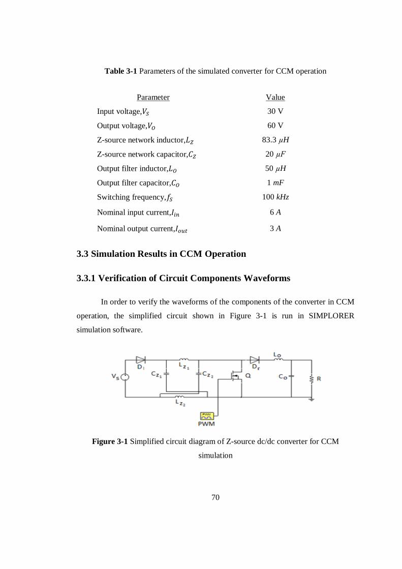
70
Table 3-1 Parameters of the simulated converter for CCM operation
Parameter Value
Input voltage, 30 V
Output voltage, 60 V
Z-source network inductor, 83.3 µH
Z-source network capacitor, 20 µF
Output filter inductor, 50 µH
Output filter capacitor, 1 mF
Switching frequency, 100 kHz
Nominal input current, 6 A
Nominal output current, 3 A
3.3 Simulation Results in CCM Operation
3.3.1 Verification of Circuit Components Waveforms
In order to verify the waveforms of the components of the converter in CCM
operation, the simplified circuit shown in Figure 3-1 is run in SIMPLORER
simulation software.
Figure 3-1 Simplified circuit diagram of Z-source dc/dc converter for CCM
simulation

71
The CCM operation using the parameters given in Table 3-1 requires that the
duty factor applied to the circuit should be 0.33 according to (3.1). Hence,
throughout the simulation the duty factor applied to the circuit model is kept constant
at 0.33.The mathematical analysis of the converter in CCM operation reveals by
(2.16) and (2.18) that the Z-source network capacitor’s average voltage, is equal
to the output voltage, . The simulation results of the converter in CCM operation
verifies that as can be seen in Figure 3-2.
Figure 3-2 Z-source network capacitor and output voltage in CCM
Figure 3-3 shows the currents belonging to the input diode , Z-source
network inductor and the output filter inductor . The PWM variation is also
shown in this figure. The first noticeable issue on the simulation results illustrated in
Figure 3-3 is that neither current nor current falls to zero as a necessary
condition for CCM operation of the converter. In the mathematical analysis part, it
has been pointed out that whenever the PWM is in “HIGH” status the input diode
is reverse biased so that the current through it becomes zero. This is really the case as
indicated by the simulation results given in Figure 3-3. Moreover the input diode
current, does not fall to zero during its conduction time interval , thus fulfilling
the second necessary condition for CCM operation.
Vo
ltag
e, V
time, ms
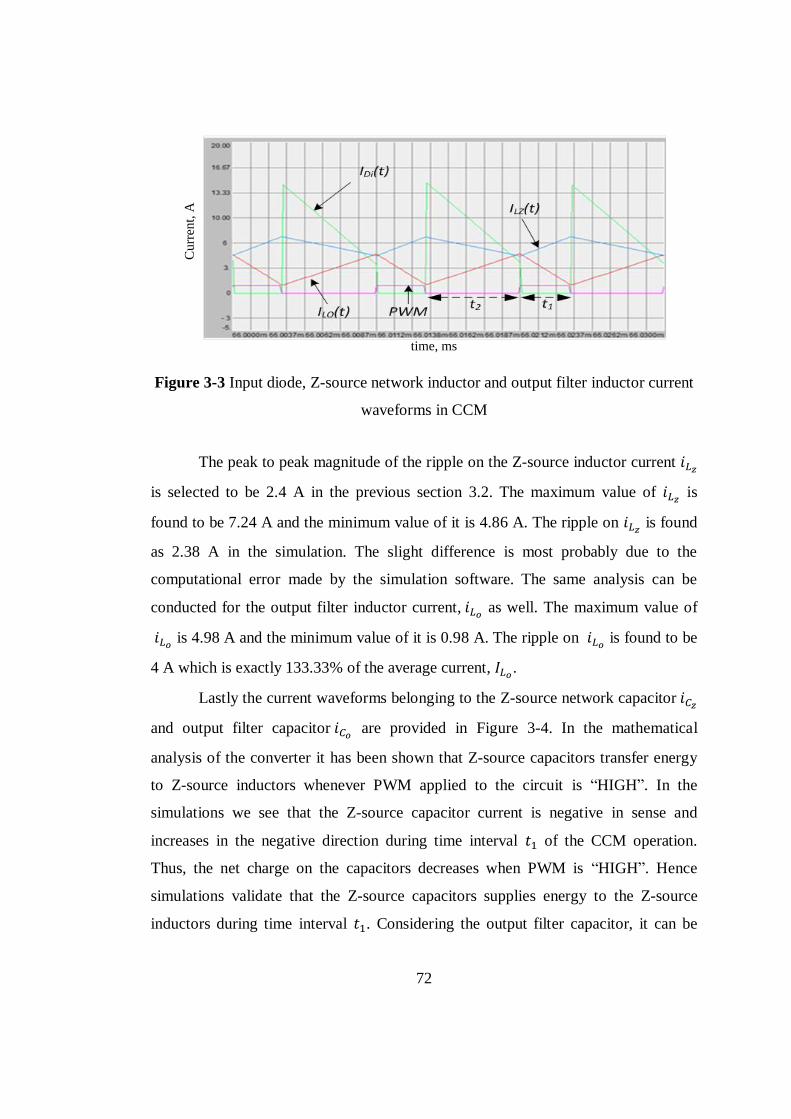
72
Figure 3-3 Input diode, Z-source network inductor and output filter inductor current
waveforms in CCM
The peak to peak magnitude of the ripple on the Z-source inductor current
is selected to be 2.4 A in the previous section 3.2. The maximum value of is
found to be 7.24 A and the minimum value of it is 4.86 A. The ripple on is found
as 2.38 A in the simulation. The slight difference is most probably due to the
computational error made by the simulation software. The same analysis can be
conducted for the output filter inductor current, as well. The maximum value of
is 4.98 A and the minimum value of it is 0.98 A. The ripple on
is found to be
4 A which is exactly 133.33% of the average current, .
Lastly the current waveforms belonging to the Z-source network capacitor
and output filter capacitor are provided in Figure 3-4. In the mathematical
analysis of the converter it has been shown that Z-source capacitors transfer energy
to Z-source inductors whenever PWM applied to the circuit is “HIGH”. In the
simulations we see that the Z-source capacitor current is negative in sense and
increases in the negative direction during time interval of the CCM operation.
Thus, the net charge on the capacitors decreases when PWM is “HIGH”. Hence
simulations validate that the Z-source capacitors supplies energy to the Z-source
inductors during time interval . Considering the output filter capacitor, it can be
Curr
ent,
A
time, ms
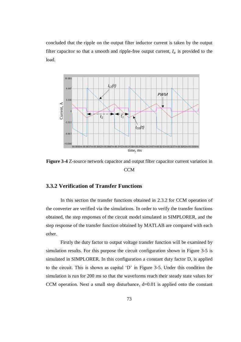
73
concluded that the ripple on the output filter inductor current is taken by the output
filter capacitor so that a smooth and ripple-free output current, is provided to the
load.
Figure 3-4 Z-source network capacitor and output filter capacitor current variation in
CCM
3.3.2 Verification of Transfer Functions
In this section the transfer functions obtained in 2.3.2 for CCM operation of
the converter are verified via the simulations. In order to verify the transfer functions
obtained, the step responses of the circuit model simulated in SIMPLORER, and the
step response of the transfer function obtained by MATLAB are compared with each
other.
Firstly the duty factor to output voltage transfer function will be examined by
simulation results. For this purpose the circuit configuration shown in Figure 3-5 is
simulated in SIMPLORER. In this configuration a constant duty factor D, is applied
to the circuit. This is shown as capital ‘D’ in Figure 3-5. Under this condition the
simulation is run for 200 ms so that the waveforms reach their steady state values for
CCM operation. Next a small step disturbance, d=0.01 is applied onto the constant
Cu
rren
t, A
time, ms

74
duty factor, D=0.33. The input voltage magnitude, capacitor and inductor sizes are
set as given in Table 3-1. The output load is set as 20Ω so that the output current is 3
A.
Figure 3-5 Circuit configurations simulated in order to verify
For dynamic response of the output voltage, Vo waveform the rise time, the
peak voltage and the damped oscillation frequency of the waveform result as in
Figure 3-6.
Figure 3-6 Dynamic response of the circuit model simulated in SIMPLORER to
verify duty factor to output voltage transfer function in CCM
A close inspection of the waveform given in Figure 3-6 reveals that the rise
time of the waveform is 1.5 ms. The peak of the overshoot in the output voltage, Vo
fdamp_osc=172.4 Hz
Vpeak=65.95
V
trise=1.5 msec
Ou
tpu
t V
olt
age,
V
time, ms

75
for the applied step disturbance is 65.95V. It is clearly seen in the figure that the
output voltage follows a damped oscillation while settling at its steady state value.
The frequency of this damped oscillation is found to be 172.4 Hz. The output voltage
settles to 63.1V at steady state after a 0.01 step change of d applied to the operating
duty factor, D=0.33.
The next step after obtaining the step response of the circuit is to determine
the duty factor to output voltage transfer function for CCM operation. The transfer
function for CCM operation was derived in 2.3.2 and is obtained as in
(2.42). The coefficients of transfer function are also found in terms of the
circuit parameters , , , , , and R. Inserting the selected parameters
given in Table 3-1 into (2.42), the duty factor to output voltage transfer function in
CCM operation is determined as in (3.6).
(3.6)
Before simulating and examining the step response of the obtained transfer
function in SIMULINK, there is one key point to be taken into consideration. The
transfer functions represent the small signal ac model of the converters. They do not
carry information about the dc operating point of the converter. They estimate how
the circuit will behave against a small perturbation applied to the control input of the
system. Control inputs of the system are duty factor or input voltage magnitude. The
dc operating points are somehow filtered while obtaining the transfer functions.
Moreover since the state space averaging technique, SSA is based on taking the
averages of the states of the converter over a switching period, the switching ripples
appearing on the component waveforms obtained by the circuit model simulation run
in SIMPLORER are not expected to be observed in the simulation result of the
transfer function by SIMULINK. In order to make the comparison of the waveforms

76
much easier, it is wise to add 60 V DC offset voltage for the simulation of the
in SIMULINK as illustrated in Figure 3-7.
Figure 3-7 Duty factor to output voltage transfer function in CCM simulated in
SIMULINK
Simulation result of transfer function in SIMULINK is displayed in
Figure 3-8.
Figure 3-8 Dynamic response of , duty factor to output voltage transfer
function in CCM obtained by SIMULINK
The simulation has been conducted with a step disturbance applied at the
instant t=200 ms. The rise time for the step response obtained from transfer function
simulated in SIMULINK is 1.5 ms as obtained in simulation by SIMPLORER. The
peak overshoot voltage is 65.55V. The step response has again damped oscillations
whose frequency is 175 Hz similar to the result obtained in simulation by

77
SIMPLORER. The steady state output voltage is obtained as 62.9V for a step
disturbance of 0.01 in duty factor. Moreover the switching ripple resulted in circuit
model simulation is not observed in the simulation results of the transfer function as
expected.
Comparing the results obtained from the circuit model simulation in
SIMPLORER and transfer function simulation in SIMULINK reveals that the results
are very close to each other. The slight differences between the two simulation
results are acceptable and the transfer function obtained makes a good approximation
for the step response of the converter against a disturbance applied to the duty factor
of the circuit.
Finally the input voltage to output voltage transfer function
will be
examined via the simulation results. The circuit model simulated in SIMPLORER is
given in Figure 3-9. The duty factor, D applied to the circuit is kept constant at 0.33
throughout the simulation. The input voltage, Vs is kept constant at 30 V for 200 ms
so that states of the system can reach steady state. At the instant t=200 ms a step
disturbance, of 1V is applied to the input voltage. The circuit parameters are again
set to the values stated in Table 3-1.
Figure 3-9 Circuit model simulated in SIMPLORER in order to verify input voltage
to output voltage transfer function,
The dynamic response of
yields the information for the rise time,
peak voltage and damped oscillation frequency of the waveform as shown in Figure
3-10.
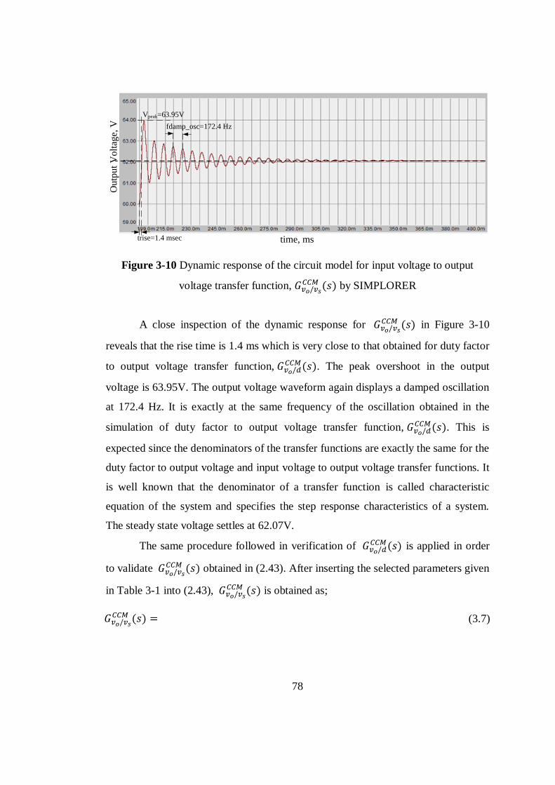
78
Figure 3-10 Dynamic response of the circuit model for input voltage to output
voltage transfer function,
by SIMPLORER
A close inspection of the dynamic response for
in Figure 3-10
reveals that the rise time is 1.4 ms which is very close to that obtained for duty factor
to output voltage transfer function, . The peak overshoot in the output
voltage is 63.95V. The output voltage waveform again displays a damped oscillation
at 172.4 Hz. It is exactly at the same frequency of the oscillation obtained in the
simulation of duty factor to output voltage transfer function, . This is
expected since the denominators of the transfer functions are exactly the same for the
duty factor to output voltage and input voltage to output voltage transfer functions. It
is well known that the denominator of a transfer function is called characteristic
equation of the system and specifies the step response characteristics of a system.
The steady state voltage settles at 62.07V.
The same procedure followed in verification of is applied in order
to validate
obtained in (2.43). After inserting the selected parameters given
in Table 3-1 into (2.43),
is obtained as;
(3.7)
Vpeak=63.95V
fdamp_osc=172.4 Hz
trise=1.4 msec
Ou
tpu
t V
olt
age,
V
time, ms

79
The simulation diagram constructed in SIMULINK is given in Figure 3-11,
and the result of the simulation is given in Figure 3-12.
Figure 3-11 Input voltage to output voltage transfer function in CCM,
simulated in SIMULINK
Figure 3-12 Dynamic response of input voltage to output voltage transfer function in
CCM,
simulated in SIMULINK
In the simulation of
the step disturbance of =1V is applied at the
instant t=200 ms. The rise time is 1.4 ms and the peak overshoot voltage is 63.89V.
Damped oscillation frequency is 175 Hz. Comparison of the results obtained by

80
circuit model simulation and transfer function simulation again reveals that the
transfer function obtained by mathematical analysis approximates the step response
well.
3.4 Simulation Results in DCM-2 Operation
3.4.1 Verification of Circuit Components Waveforms
In order to verify the waveforms of the components of the converter in DCM-
2 operation, the circuit illustrated in Figure 3-1 is simulated in SIMPLORER with
different operating condition. In order to force the converter to operate in DCM-2
mode, the input voltage is decreased to 20 V and the load is decreased to 1.5 A, in
other words . The parameters of the converters used in simulations for
DCM-2 mode are provided in Table 3-2.
Table 3-2 Parameters of the simulated converter for DCM-2 operation
Parameter Value
Input voltage, 20 V
Output voltage, 60 V
Z-source network inductor, 83.3 µH
Z-source network capacitor, 20 µF
Output filter inductor, 50 µH
Output filter capacitor, 1 mF
Switching frequency, 100 kHz
Nominal input current, 4.5 A
Nominal output current, 1.5 A
In DCM-2 mode of operation the input-output voltage relationship is found as
given in (2.77). In this equation the parameter depends on the switching

81
frequency, duty factor, and the load as stated in (2.79). Using these two equalities
it is possible to conclude that the duty factor applied to the circuit must be 0.38 in
order to obtain 60 V output voltage. The critical load for the applied duty factor is
found to be 26Ω by (2.83). Since condition is satisfied with preset
load, the converter will operate in DCM-2 mode. In this case is found to be 0.28.
In DCM-2 mode of operation the average Z-source capacitor voltage, is
not equal to the output voltage according to the results obtained in (2.63) and (2.77).
With the given operating conditions, although the output voltage is 60 V, the Z-
source capacitor voltage is found to be 55.4V regarding (2.63) . This is also verified
by the simulation results of the converter in DCM-2 mode shown in Figure 3-13.
Figure 3-13 Z-source network capacitor voltage and the output voltage in DCM-2
mode of operation
Figure 3-14 shows currents belonging to the input diode , Z-source network
inductor and the output filter inductor and PWM variations in DCM-2 mode
of operation. As seen from Figure 3-14 the Z-source network inductor current never
falls to zero during the operation. On the other hand, the output filter inductor current
falls to zero in DCM-2 operation as seen from the simulation result. Whenever the
PWM is “HIGH”, the input diode is reverse biased again and does not let the current
flow through it. However when PWM is “LOW” the input diode conducts. The input
Vo
ltag
e, V
time, ms

82
diode current never falls to zero during the time interval t3. When PWM is HIGH, the
Z-source capacitors transfer energy to the Z-source inductors as mentioned before.
This is also understood from the simulation results since current increases during
t1+t2 period, in other words energy is stored in these inductors. During t1 period the
load is supplied by the output filter inductor and capacitor. However current falls
to zero and stops to transfer energy at the start of t2 period. Hence during t2
transfers the required energy to the load alone since the rectification diode does not
conduct. This is the fundamental requirement of DCM-2 operation. When PWM
switches into the LOW state, again starts to conduct and as a result current
starts to increase. During this t3 period, the Z-source inductors transfer the energy
stored on them to the load side via the rectification diode. This is the reason why
current falls during t3 period. Finally during t3, the current drawn from the source
energizes the Z-source capacitors.
Figure 3-14 Current waveforms belonging to input diode, Z-source network inductor
and output filter inductor in DCM-2 operation
Finally the Z-source network capacitor and output filter capacitor current
waveforms are provided in Figure 3-15. As mentioned before when PWM is HIGH
transfers energy which is understood from the negative capacitor current during
this period. In addition to that current decreases during t1 which shows that it
Curr
ent,
A
time, ms

83
transfer energy to the load. The noticeable issue on current is that its value is
constant during t2 which proves that the load is fed only by .Since the output
voltage is 60 V and load is 40Ω, the output filter capacitor current is constant at -1.5
A during t2. The positive current of indicates that it accumulates charge on it
during t3 period. A careful investigation of Figure 3-14 and Figure 3-15 reveals that
during t3 period, the ripple current of is absorbed by .
Figure 3-15 Current waveforms belonging to Z-source network capacitor and output
filter capacitor in DCM-2 operation
3.4.2 Verification of Transfer Functions
In this section the transfer functions obtained in 2.3.4 for DCM-2 operation of
the converter are verified via the simulations. The procedure to be followed for
DCM-2 operation will be the same with that applied for CCM operation. The step
response of the circuit model operated in DCM-2 is obtained by simulation in
SIMPLORER and the step responses of the derived transfer functions are obtained
by MATLAB.
The circuit model illustrated in Figure 3-5 is again simulated in SIMPLORER
in order to verify the duty factor to output voltage transfer function with the given
parameters in Table 3-2. Constant duty factor D is set as 0.38. The simulation is
Cur
rent
, A
time, ms

84
again run for 200 ms so that the waveforms reach their steady state values for DCM-
2 mode of operation. The step disturbance of d=0.01 is applied to the duty factor, D
at t=200 ms. The simulation result of the circuit model is as displayed in Figure 3-16.
Figure 3-16 Dynamic response of the circuit model simulated in SIMPLORER to
verify duty factor to output voltage transfer function in DCM-2 of operation
When examined of the waveform illustrated in Figure 3-16 reveals that the
converter behaves as an overdamped system in DCM-2 of operation. It does not
exhibit damped oscillations or overshoot while reaching steady state. The settling
time is longer for overdamped systems relative to underdamped or critically damped
systems. The settling time is 43.2 ms and the output voltage settles at 65.58V at
steady state against d=0.01 step change on the operating duty factor, D.
It is now necessary to obtain the step response of the derived duty factor to
output voltage transfer function for DCM-2 operation. The mathematical calculation
is conducted in 2.3.4 and is obtained as given in (2.127). The coefficients
of transfer function are needed to be determined according to the
parameters given in Table 3-2. Doing the necessary calculations the duty factor to
output voltage transfer function in DCM-2 operation is found as follows:
(3.8)
tss=43.2 msec
Vss=65.58V
Outp
ut
Volt
age,
V
time, ms

85
It is previously mentioned in CCM transfer function analysis part that, the
step response of a transfer function helps us to estimate only the small signal ac
characteristics of a system. Hence it is again a good approach to add the dc output
voltage as an offset in simulation in SIMULINK so that the comparison of the
waveforms will be much understandable. The simulation diagram constructed in
SIMULINK is given in Figure 3-17.
Figure 3-17 Duty factor to output voltage transfer function in DCM-2 of operation
simulated in SIMULINK
Simulation result of transfer function in SIMULINK is displayed in
Figure 3-18.
Figure 3-18 Dynamic response of , duty factor to output voltage transfer
function in DCM-2 mode of operation obtained by SIMULINK

86
The step disturbance is again applied at 200 ms. The step response of the
transfer function does not exhibit damped oscillations. It takes 42.5 ms to reach the
steady state in simulation. The steady state voltage is obtained as 65.81V in
SIMULINK for a step disturbance of d=0.01 on the duty factor, D. Comparison of
the results obtained by the circuit model and transfer function simulation reveals that
the steady state voltages and time to reach the steady state are very close in both
simulations. Hence the derived transfer function is a good approximation for the
converter operating in DCM-2 mode of operation.
Next, the input voltage to output voltage transfer function is needed to be
validated via the simulation results. The circuit model illustrated in Figure 3-9 is
again simulated in SIMPLORER with the parameter set as given in Table 3-2. The
duty factor, D applied to the circuit is kept constant at 0.38 in order to obtain 60 V
output voltage, Vo throughout the simulation. The input voltage, Vs is kept constant
at 20 V for 200 ms. so that the waveforms reach the steady state. A step disturbance,
of 1V is applied to the input voltage at t=200 ms. The simulation result of the
circuit model is shown in Figure 3-19.
Figure 3-19 Dynamic response of the circuit model simulated by SIMPLORER to
verify input voltage to output voltage transfer function in DCM-2 mode of operation
tss=43.3 msec
Vss=63.08V
Outp
ut
Volt
age,
V
time, ms

87
The converter operating in DCM-2 mode again exhibits an overdamped step
response for an input voltage step disturbance, . The settling time is 43.3 ms
against 1V step disturbance application and the output voltage settles at 63.08V at
steady state.
Lastly, the step response of the derived input voltage to output voltage
transfer function in (2.132) should be verified via simulation in SIMULINK. The
coefficients of
transfer function in DCM-2 operation are calculated using
the parameters given in Table 3-2.
is found as follows:
(3.9)
The simulation diagram constructed in SIMULINK is given in Figure 3-20,
and the result of the simulation is given in Figure 3-21.
Figure 3-20 Input voltage to output voltage transfer function in DCM-2 mode of
operation simulated in SIMULINK
Figure 3-21 Dynamic response of
, input voltage to output voltage transfer
function in DCM-2 mode of operation obtained by SIMULINK

88
In simulation of
obtained for DCM-2 mode of operation in
SIMULINK, the step disturbance of 1V is applied at t=200 ms. The time to reach
steady state takes 46.7 ms. The output voltage settles at 63.21V at steady state in the
simulation of the transfer function. Comparing the results of the circuit model and
transfer function shows that there are slight differences between them. These
differences are acceptable because of the assumptions made in the derivation of the
small signal ac model of the converter in DCM-2 mode and the transfer function
still approximates the dynamic response of the converter in DCM-2 mode
of operation.

89
CHAPTER 4
CONTROLLER DESIGN OF Z-SOURCE DC/DC
CONVERTER
4.1 Introduction
In this chapter the controller design of the implemented circuit will be given.
In the design process of the controller we will make use of the transfer functions
obtained and verified previously.
The implemented converter circuit is supposed to operate properly within an
input voltage range of 18-32V. The load regulation is desired to be less than 5%
within a load range of zero to 3 A. The controller performance is the most crucial
part of the system in order to achieve the mentioned goals about the regulation of the
converter.
The controller can be implemented in analog or digital form. For the analog
control form there are three well known compensator topologies: Type I, type II and
type III compensators. The compensators are implemented using capacitors, resistors
and error amplifiers. All three compensator structures are different from each other in
terms of the circuit layouts. Hence, it is constructed by bringing the necessary
infrastructures on the circuit board together in case a different compensator type is to
be utilized for the controller design. In addition, the poles and zeros of the analog
compensators are set by suitably selected capacitors and resistors. The pole and zero

90
locations of the controller determined in the simulation may slightly differ than the
ones applied to the circuit. This is expected since the transfer functions are obtained
assuming that the components of the converter are ideal. In this case it is necessary to
change the size of the capacitors and resistors which make the realization of the
controller more difficult. However digital controller parameters being set in software,
it is easy to change the controller parameters for trimming in software which
provides advantage. The main disadvantage of the digital control is the time delay
caused by the digital controller due to the computations done during the
implementation. If it takes too much to generate the necessary PWM signal the
controller will not be able to close the control loop. The system will respond too late
to the changes observed at the output voltage. This might cause indefinite oscillations
at the output voltage and result in an unstable system. In order to overcome this
disadvantage the digital controller must be able to complete the necessary
computations less than a PWM period. By this way the delay caused by the
computations will not affect the controller performance. Microchip has special digital
controllers designed for SMPS applications. The computation time for the required
PWM can be lowered below 10us with an efficient code embedded into dsPIC series
products. Among this family dcPIC30F2020 is selected in the application since it has
the necessary analog-to-digital conversion channels, PWM output channel and
general purpose input/output channels.
There are two options for the controller design in literature: voltage mode
control or current mode control. Either can be applied in order to implement the
controller. In voltage mode control there is only one control loop. The output voltage
feedback is taken and compared with the predetermined reference in voltage mode
control technique. It is simpler than the current mode control. However the dynamic
performance of the controller obtained in voltage mode control is poorer relative to
the one obtained with current mode control. In current mode control there is an
additional inner loop for the current compensation which makes the system faster. In
current mode control the Z-source network inductor current and the output voltage

91
are controlled in cascaded manner. The outer control loop is required for the output
voltage regulation. The output of the outer controller loop becomes the reference for
the inner loop which is required for current regulation of the Z-source network
inductor. For the controller designs of the outer and inner loops, one can adopt using
a PI control scheme. The proportional term makes the system faster. The settling and
rise times of a system can be lowered with a well selected proportional term. The
integral term is required in order to achieve zero steady-state error. Hence with PI
control scheme it is possible to obtain a satisfactory dynamic performance in terms of
settling time and steady-state error.
So far the general controller structure is discussed. In the rest of this chapter
the control block diagram of the converter will be developed. The voltage-loop and
current-loop controllers will be designed utilizing the PI control scheme. The
simulation results of the converter with the designed controller implemented will be
given. Finally the domain conversion calculation is given at the end of this chapter.
Domain conversion is necessary in order to map the controller parameters obtained
in s-domain into z-domain. By this way the parameters can be directly inserted to the
code which will be embedded into dsPIC30F2020.
4.2 Controller Design
In this part the controller design of the converter will be explained in detail.
In designing the controller the transfer functions describing the dynamic models of
the converter in CCM and DCM-2 modes of operations will be utilized. The
performance of the controller will be examined via the simulation results.
In the controller design of the Z-source converter both the current- and
voltage-loop will be controlled. Hence it is necessary to design two controllers for
the converter. The control block diagram of the converter is shown in Figure 4-1. As
seen from Figure 4-1 there is one inner loop; current-loop, and an outer loop;
voltage- loop in the control block diagram. The main purpose of the controller for the
converter is to produce the required duty factor for the proper operation. The

92
converter itself takes the duty factor applied as an input and produces the output
voltage and the Z-source network inductor current as outputs.
Figure 4-1 Control block diagram of the converter
The followings used in the block diagram are defined as;
: Reference output voltage
: Output voltage error
: Output voltage feedback
: reference current
: current error
: current feedback
: Applied duty factor
: Voltage loop controller
: Current loop controller
(Duty factor-to-output voltage transfer function)
(Duty factor-to- current transfer function)
Referring to Figure 4-1 the difference between the reference voltage,
and the output voltage feedback, is called the voltage error, . It is the input for
the voltage-loop controller. The output of the voltage-loop controller is the reference
input for the current control loop. The difference between the current feedback and
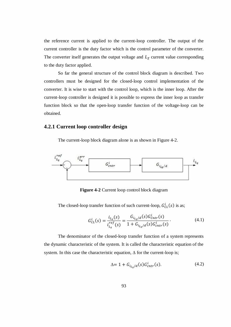
93
the reference current is applied to the current-loop controller. The output of the
current controller is the duty factor which is the control parameter of the converter.
The converter itself generates the output voltage and current value corresponding
to the duty factor applied.
So far the general structure of the control block diagram is described. Two
controllers must be designed for the closed-loop control implementation of the
converter. It is wise to start with the control loop, which is the inner loop. After the
current-loop controller is designed it is possible to express the inner loop as transfer
function block so that the open-loop transfer function of the voltage-loop can be
obtained.
4.2.1 Current loop controller design
The current-loop block diagram alone is as shown in Figure 4-2.
Figure 4-2 Current loop control block diagram
The closed-loop transfer function of such current-loop, is as;
(4.1)
The denominator of the closed-loop transfer function of a system represents
the dynamic characteristic of the system. It is called the characteristic equation of the
system. In this case the characteristic equation, for the current-loop is;
(4.2)

94
By definition the characteristic equation, of a system is as follows;
(4.3)
Hence the open-loop transfer function of the above system, is as
follows;
(4.4)
In order to design a controller for a system it is enough to know the open-loop
transfer function of that system. In the current loop controller design the Z-source
network inductor current, will be utilized. Hence it is necessary to use the duty
factor to inductor current transfer function which is obtained in (2.44). The transfer
function coefficients depend on the circuit parameters, . Hence
for different load and input voltage conditions different transfer functions result and
they represent the dynamic model of the system at low frequencies. The low
frequency behaviors of these different transfer functions obtained at different
operating points are close to each other. In other words the pole and zero locations of
the characteristic equations of these different transfer functions do not change
considerably.
For the controller design at a certain operating point one uses the stationary
parameters of the circuit, such as inductor and capacitor sizes, and the selected load
and input voltages to obtain the transfer function. In general the controller is
designed by considering the full load condition under nominal input voltage value.
The full load current rating of this converter is 3 A and the nominal input voltage is
30 V as mentioned before. Hence the parameters given in Table 3-1 are used in to
design the current loop controller. Using the parameters given in Table 3-1,
is obtained as;
(4.5)

95
The pole-zero map of the transfer function in (4.5) is shown in Figure 4-3.
Figure 4-3 Pole-zero map of
In Figure 4-3 ‘x’ shows the locations of poles, and ‘o’ shows the locations of
zeros of the transfer function. Note that none of the poles are on the right half
complex plane in Figure 4-3 indicating that the system represented by the transfer
function is stable. In addition none of the zeros are on the right half complex plane.
Such kinds of systems are known as minimum phase systems which are relatively
easier to stabilize.
Before beginning the controller design, the bode diagram of the transfer
function must also be obtained so that the phase and gain margins of the system can
be identified and the frequency locations where some poles or zeros must be added

96
can be determined. Bode diagram of the system is obtained with MATLAB and
given in Figure 4-4.
Figure 4-4 Bode diagram of
In order to compensate the current control loop, a PI controller will be
utilized. PI controller is the most common controller technique used in literature. In
general it is known that the derivative term in a PID controller is sensitive to the
noise involved with the measured data. Hence it is usually excluded in the controller
design. The transfer function of a PI controller is as follows.
(4.6)
shows the proportional gain constant of the current controller in (4.6).
This term is necessary to obtain a quick and satisfactory response. The rise time
settling time and percentage magnitude of the overshoot, all depend on the
proportional gain constant. term in the equality above represents the integral gain
constant of the current controller. term is necessary in order to obtain a zero
steady state error in the closed-loop operation. The transfer function of the current
loop controller has a pole at zero frequency. term determines the gain of the
current loop controller. Moreover the controller has a zero whose location is
PM=90°

97
determined with the selected and
terms. Hence the controller design of the
current loop is actually setting the gain of the controller and determining the location
of the zero of the controller.
The phase margin of the open-loop transfer function is 90⁰ and the gain
margin is positive. The open-loop transfer function itself is stable. However in
literature it is highly recommended to obtain a phase margin of 45⁰-60⁰ due to the
stability concerns. A great phase margin makes the system slower and the system
becomes overdamped. A smaller phase margin, however, makes the system much
faster while making the system less resistant to the disturbances that the converter is
exposed to. A phase margin of 45⁰-60⁰ actually represents a system having critically
damped response to a step input. Hence it is a reasonable choice to adjust the phase
margin of the open-loop transfer function of the current loop controller to 45⁰-60⁰.
MATLAB has a toolbox called SISOTOOL which is used for controller design. In
SISOTOOL it is possible to add poles and zeros to the controller transfer function
and change the locations of the added poles and zeros. Moreover the gain of the
controller can be set in an online manner. With a proportional gain constant of
0.0045 and integral gain constant of 10, a reasonable phase and gain margin is
obtained. With the selected proportional and integral gain constants the controller
transfer function of the current loop is obtained as follows.
(4.7)
The bode plot for the open-loop transfer function, is shown in Figure
4-5 with the designed current loop controller.
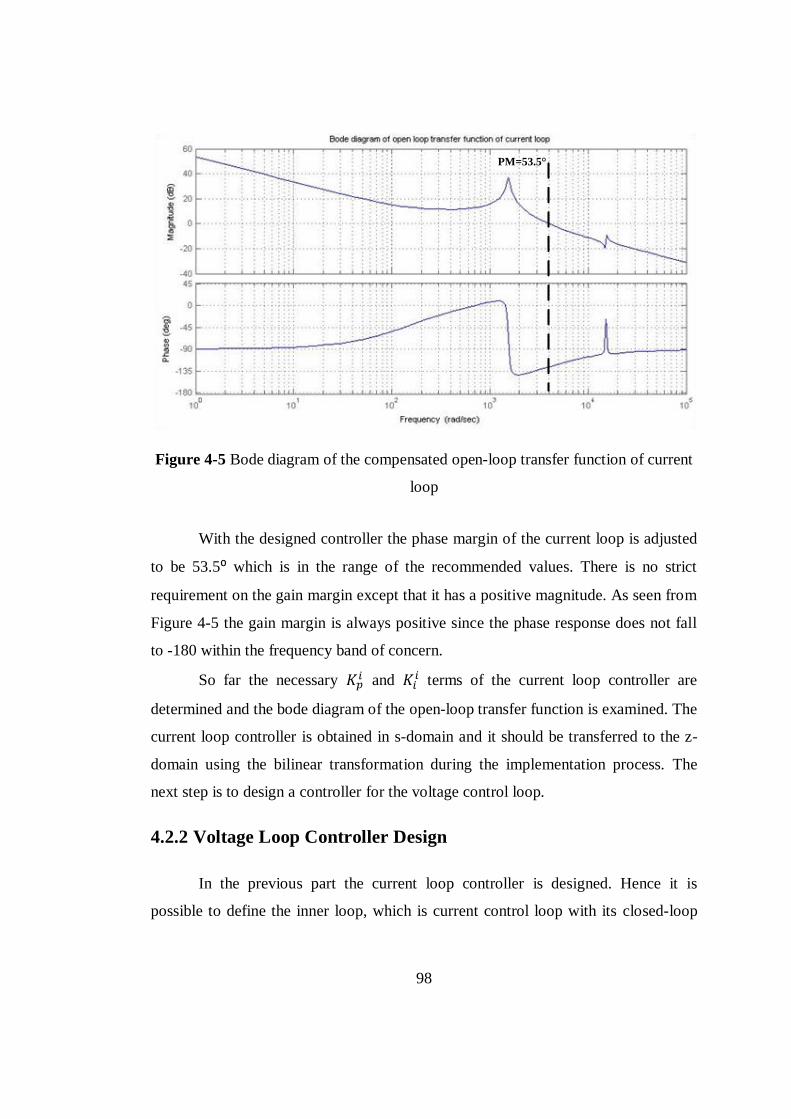
98
Figure 4-5 Bode diagram of the compensated open-loop transfer function of current
loop
With the designed controller the phase margin of the current loop is adjusted
to be 53.5⁰ which is in the range of the recommended values. There is no strict
requirement on the gain margin except that it has a positive magnitude. As seen from
Figure 4-5 the gain margin is always positive since the phase response does not fall
to -180 within the frequency band of concern.
So far the necessary and
terms of the current loop controller are
determined and the bode diagram of the open-loop transfer function is examined. The
current loop controller is obtained in s-domain and it should be transferred to the z-
domain using the bilinear transformation during the implementation process. The
next step is to design a controller for the voltage control loop.
4.2.2 Voltage Loop Controller Design
In the previous part the current loop controller is designed. Hence it is
possible to define the inner loop, which is current control loop with its closed-loop
PM=53.5°

99
transfer function. Referring to the Figure 4-1, the closed-loop transfer function of the
current loop can be defined as the following:
(4.8)
In (4.8), stands for the closed-loop transfer function of
the current loop shown in Figure 4-1. The voltage loop control block diagram is
illustrated in Figure 4-6.
Figure 4-6 Voltage loop control block diagram
The closed-loop transfer function of the voltage loop can be determined as
follows:
(4.9)
Using the definition of given in (4.8), and rewriting (4.9)
the characteristic equation of the voltage loop, is obtained as follows:
(4.10)
Hence the open-loop transfer function of the voltage loop, can be
obtained as;
(4.11)

100
As seen from (4.11), the open-loop transfer function of the voltage loop is not
the product of the other transfer functions in the loop. Hence the voltage loop
controller cannot be designed with the traditional bode plot approach which was
applied in the design process of the current loop controller. It is necessary to try
different proportional and integral gains for the controller and check whether the
required phase- and gain-margins are obtained or not. It is a time-consuming but easy
design procedure with the utilization of MATLAB SISOTOOL toolbox. However
obtaining the necessary phase- and gain-margins for the open-loop transfer function
is not satisfactory for achieving the stability of the voltage control loop.
Z-source converter has two inductors and two capacitors due and a careful
investigation of the duty factor-to-output voltage transfer function shows that it
has a right half plane zero. This can be confirmed by examining the pole-zero map of
of the converter shown in Figure 4-7 obtained with MATLAB.
Figure 4-7 Pole-zero map of
The systems having at least one right half plane zero are called the non-
minimum phase systems. These systems are more difficult to compensate relative to
the minimum phase systems. Obtaining the recommended phase- and gain-margins

101
for the open-loop transfer function of non-minimum phase systems does not mean
that the system is closed-loop stable. It is necessary to verify that the system does not
have right half plane zero with the designed controller.
After several trials the proportional and integral gains of the voltage loop
controller are selected as 0.5 and 1000, respectively. Hence the voltage loop
controller can be defined as follows:
(4.12)
In order to verify the designed voltage loop controller the bode diagram of the
open-loop transfer function of the voltage loop is obtained and shown in Figure 4-8.
Figure 4-8 Bode diagram of the compensated open-loop transfer function of voltage
loop
With the designed controller the phase-margin of the voltage loop is adjusted
to 53.4⁰ which is in the range of the recommended phase-margin in literature. As
seen from Figure 4-8 the gain margin is again always greater than zero since the
phase never falls to -180⁰ within the frequency band of concern.
PM=53.4°

102
Finally the minimum phase property of the open-loop transfer function of the
voltage loop must be checked in order to state that the system will be closed-loop
stable. The pole-zero map of with the designed controller is given in Figure
4-9
Figure 4-9 Pole-zero map of
As seen from Figure 4-9 there is not any right half plane zero in the open-
loop transfer function of the voltage loop. In other words the designed controller
shifts the right half plane zero to the left half plane. Hence the phase- and gain-
margin results obtained with bode diagram approach are trustable. The system is
closed-loop stable with the designed controller.
4.3 Simulation Results of the Closed-Loop System
In this part the designed controllers will be verified via the simulations run in
SIMPLORER. The designed converter is supposed to operate with an input voltage
of 18V to 32V range. The load is supposed to change from no-load to 3 A full-load.
The components are selected so as to operate the converter both in CCM and DCM-2
mode of operation. Hence the designed controllers must be able to regulate the
output voltage both in CCM and DCM-2 mode of operation.

103
For the verification of the designed controllers the full-bridge Z-source dc/dc
converter is simulated in SIMPLORER. The controllers are inserted into the
simulation model and converter is run in a closed-loop control manner. The closed-
loop simulation model of the converter is given in Figure 4-10.
Figure 4-10 Closed-loop simulation model of Z-source dc/dc converter
In Figure 4-10 the red signals represent the voltage and current feedbacks.
The output voltage is set at 60 V; hence VREF is set at 60 V in simulation. As
mentioned earlier the output of the voltage controller is the reference for the current
loop. The output of the current-loop controller is duty-factor necessary for the proper
operation of the converter. The duty-factor generated enters the gate drive signal
generation block. This block is necessary to generate the gate drive signals required
by Q1, Q2, Q3 and Q4. When PWM is “HIGH”, all the switches in full-bridge are
conducting. Hence, the input terminal of the isolation transformer is shorted and
shoot-through mode of operation is achieved. When PWM is low one of the switch
pairs, either “Q1, Q4” or “Q2, Q3” are conducting. These conducting switching pairs
follow each other during the operation. For example if “Q1, Q4” are conducting in the
first period, “Q2, Q3” will be conducting in the next period. In this way an ac square
waveform is applied to the input of the transformer.

104
In order to determine the performance of the designed controllers step load
and input voltage changes are applied to the converter in simulation. The input
voltage is raised from 18V to 32V under full-load and 10% load conditions. In
addition to that the load is changed from full-load to no-load and under an input
voltage of 18V and 32V, respectively. In this manner the converter is operated both
in CCM and DCM-2 modes of operation. As a result the controller performance is
verified both in CCM and DCM-2 modes of operation of the converter. The
simulation results are summarized in Table 4-1.
Table 4-1 Simulation Results of the Converter against Step Disturbances
Input Voltage Load Figure
Fixed at 32V 3 A-to-0.3 A-to-3 A Figure 4-11
Fixed at 18V 3 A-to-0.3 A-to-3 A Figure 4-12
18V-to-32V-to-18V Fixed at 3 A (100% load) Figure 4-13
18V-to-32V-to-18V Fixed at 0.3 A (10% load) Figure 4-14
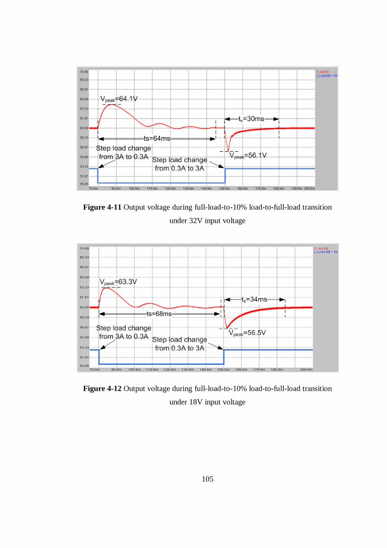
105
Figure 4-11 Output voltage during full-load-to-10% load-to-full-load transition
under 32V input voltage
Figure 4-12 Output voltage during full-load-to-10% load-to-full-load transition
under 18V input voltage
ts=64ms
ts=68ms
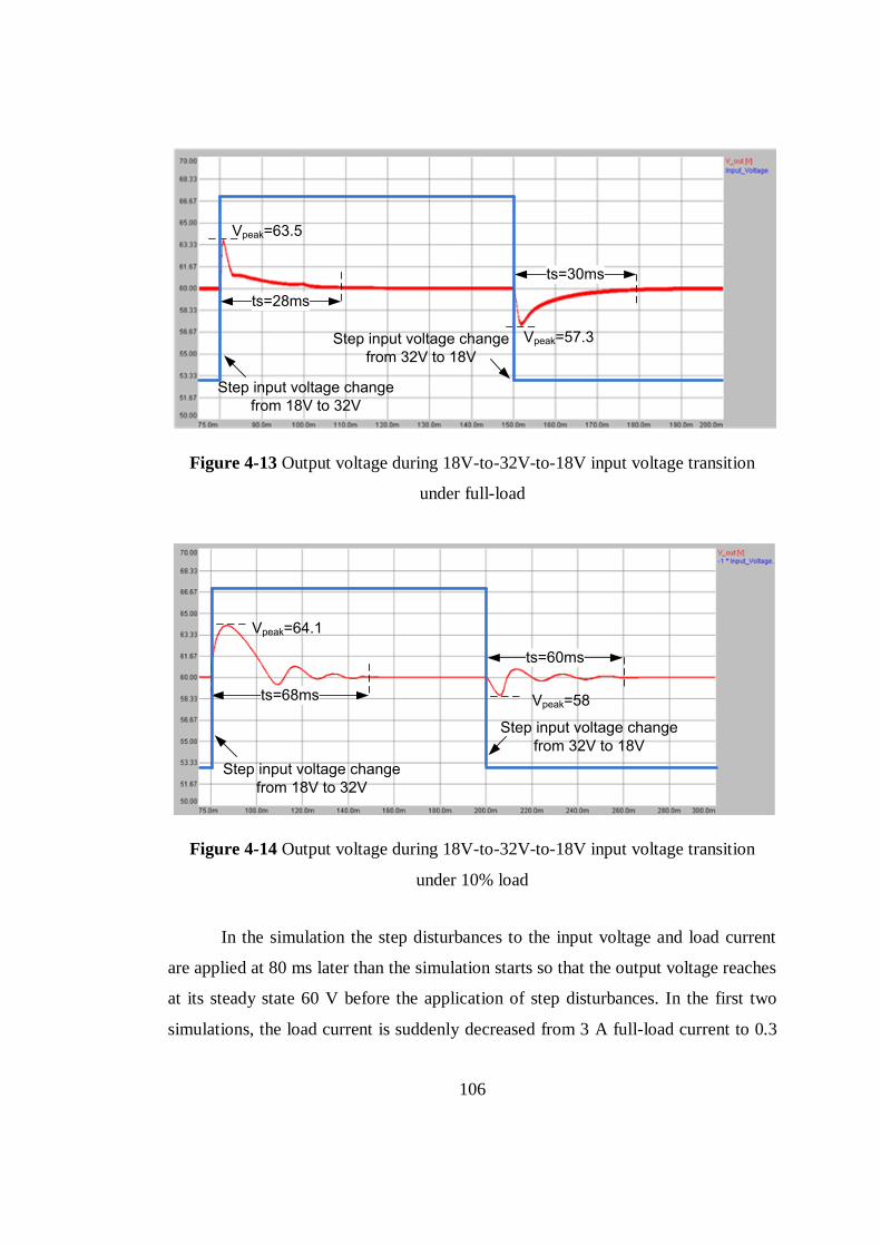
106
Figure 4-13 Output voltage during 18V-to-32V-to-18V input voltage transition
under full-load
Figure 4-14 Output voltage during 18V-to-32V-to-18V input voltage transition
under 10% load
In the simulation the step disturbances to the input voltage and load current
are applied at 80 ms later than the simulation starts so that the output voltage reaches
at its steady state 60 V before the application of step disturbances. In the first two
simulations, the load current is suddenly decreased from 3 A full-load current to 0.3
Vpeak=63.5
Vpeak=57.3
ts=28ms
ts=30ms
Step input voltage change
from 18V to 32V
Step input voltage change
from 32V to 18V
Step input voltage change
from 18V to 32V
Step input voltage change
from 32V to 18V
ts=68ms
ts=60ms
Vpeak=58
Vpeak=64.1

107
A at t=80 ms while keeping the input voltage fixed. The peak overshoot voltage and
settling time are shown in the figures displaying the simulation results. For the
simulation results given in Figure 4-11 and Figure 4-12 50 A offset current is added
to the load current so that the output voltage and load current variations can be
observed simultaneously.
The simulation results verify that the designed controllers operate well in the
operating range of the converter. The system is prevented being unstable due to the
step disturbances applied to the input voltage and load current via the controllers.
Moreover throughout the simulation the converter operates both in CCM and DCM-2
modes due to the load and input voltage disturbances applied. Hence the designed
controllers function properly both in CCM and DCM-2 mode of operation of the
converter.

108
CHAPTER 5
EXPERIMENTAL RESULTS OF Z-SOURCE DC/DC
CONVERTER
5.1 Introduction
In this chapter the experimental results of the implemented prototype
converter is presented. The circuit is operated in open-loop control and closed-loop
control modes. The open-loop control mode results are taken in order to verify
voltage and current waveforms obtained via simulations in Chapter 3 and make a
comparison of the theoretical work and experimental measurements. In the closed-
loop control mode, the performance of the controller designed in Chapter 4 is
examined. The dynamic responses of the converter under certain operating
conditions are given in this part of the work. Finally the efficiency of the converter is
calculated theoretically and it is compared with that experimentally measured. The
circuit schematics of the implemented converter are given in Appendix B. The
prototype converter has four layers. However, only the top and bottom views of the
layout are given in Appendix C. The photos of the prototype converter with the
description of the used components are given in Figure 5-1 and Figure 5-2.

109
Figure 5-1 Top view of the prototype converter
Figure 5-2 Bottom view of the prototype converter
5.2 The Experimental Results in Open-Loop Control
The prototype converter is operated in open-loop control mode so as to verify
simulation results of the voltage and current waveforms given in Chapter 3. In
Chapter 3, the simulations are made for both CCM and DCM-2 operation. In order to
verify the simulation results the converter should be operated both in CCM and
DCM-2 operations.

110
5.2.1 Open-Loop Control CCM Operation Experimental Results
The open-loop control CCM operation of the converter is implemented with
the following parameters: The input voltage is given by HP6032A dc power supply
and adjusted to 30 V. The duty factor and frequency of PWM signal applied to the
converter are set as 0.338 and 100 kHz by the software embedded into the digital
signal controller. A dc electronic load (HP 6050A) is used in order to sink current
from output of the converter. The current delivered to the load is set as 3 A so that
the implemented and the simulated converter have exactly the same operating
conditions. By this way a reasonable comparison of the simulation and experimental
results can be done.
The Z-source inductor current and voltage waveforms against the applied
duty factor are given in Figure 5-3.
Figure 5-3 Voltage and current waveforms of against applied PWM in CCM
The maximum and minimum values of are 8.32 A and 5.68 A,
respectively. However, they were found to be 7.24 A and 4.86 A in the simulation
results. The difference between the experimental and the simulation results is due to
the fact that the components in the implemented converter are not ideal. Non-ideal
𝑊𝑀
𝑧( )
𝑧( )
𝑧 = 8.32 A
𝑧 = 5.68 A
𝑧 = 61 V
𝑧 = -31 V

111
components in the implemented converter causes more current to be drawn from the
input supply due to the additional losses. It is mentioned earlier that, the average
current drawn from the supply is equal to the average current flowing through .
The average current increases as the current drawn from supply increases. Hence
it is expected that, the maximum and minimum values of current in the
implemented circuit to be slightly greater than the ones obtained by simulation. The
ripple magnitude of the current waveform of the implemented circuit is 2.64 A and it
is very close to the simulation results. The maximum and minimum values of
inductor voltage are 61V and -31V respectively. It is expected to observe 60 V and -
30 V on theoretically. Hence the experimental results are very close to the
theoretical results. The voltage waveform has spikes coinciding with the current
direction change instants. The stray inductance in the converter might cause a voltage
spike to be observed, since changes sign at these transition instants.
Figure 5-4 shows the current and voltage waveforms of the output filter
inductor during the CCM operation of the converter. The maximum and minimum
values of current are found to be 4.98 A and 0.98 A, respectively in the
simulation. As expected the maximum and minimum values obtained in experimental
results are slightly greater due to the non-ideal components of the converter. The
maximum and minimum values of the output filter inductor current are found to be
5.30 A and 0.68 A respectively in the experimental results. As seen from Figure 5-4
the output filter voltage waveform exhibits ringing throughout the operation. This is
due to the leakage inductance of the isolation transformer and the reverse recovery
current of output rectifier diodes. The transformer’s secondary leakage inductance
and the capacitance of the rectifier diode determine the frequency of the ringing. The
ringing occurs whenever the voltage waveform changes from -59V to 31V. This does
not happen during the transition of the voltage waveform from 31V to -59V. This is
actually an indication of the fact that the ringing is due to reverse recovery charge of
the rectifier diode. Referring to Figure 5-32 it can be concluded that, conducting
diode pair change in each switching cycle on the falling edge of the applied PWM

112
signal. Note that ringing phenomena is observed at the falling edge of the applied
PWM signal according to Figure 5-4. Hence it can be concluded that the reverse
recovery current, or the charge stored in the rectifier diode, causes ringing in the
voltage waveform of the filter inductor. The final voltage value of the output filter
agrees with the mathematical analysis results.
Figure 5-4 Voltage and current waveforms of against applied PWM in CCM
The Z-source capacitor voltage waveform during CCM operation is shown in
Figure 5-5. On the left side of the figure the measurement is taken with dc coupling.
The average of the waveform is 60 V, which verifies the simulation results and the
mathematical analysis of CCM operation. It is also equal to the output voltage as
mentioned in (2.16) and (2.18). In mathematical analysis part it is mentioned that,
whenever PWM is ‘high’, the capacitor voltage decreases, which means that the
capacitors transfer energy to the inductors in Z-source network impedance. This is
also verified by the experimental results. Moreover, according to Figure 5-5
whenever PWM is ‘low’, the capacitor voltage increases which shows that it is
charged from the input supply.
𝑊𝑀
= 31 V
= -59 V
= 5.3 A
= 0.68 A
( )
( )

113
Figure 5-5 voltage waveform against applied PWM in CCM, a) dc coupling, b) ac
coupling
The output voltage of the converter is shown in Figure 5-6. On the left side of
Figure 5-6, the voltage measurement is taken with dc coupling and it shows that the
output voltage is exactly 60 V. On the right side of Figure 5-4 the ac coupling
measurement of the output voltage is provided. Whenever the PWM is ‘high’ the
output filter capacitor and inductor transfers the required energy to the load. Hence
the filter capacitor voltage, which is the output voltage, decreases when PWM is
‘high’. On the other side when PWM is ‘low’, the energy stored in Z-source
inductors are transferred to the load side and the filter capacitor voltage increases. It
is worth to note that there is voltage spike on the output voltage at the switching
frequency. High and stresses during the switching instants might cause
this voltage spike.

114
Figure 5-6 Output voltage waveform against applied PWM in CCM, a) dc coupling,
b) ac coupling
Finally for the sake of completeness the voltage waveforms across the input
diode, full bridge MOSFETs and primary side of the transformer are provided in
Figure 5-7. From the input diode anode-cathode voltage waveform, it is seen that
when PWM is ‘high’, the input diode is reverse biased at -90 V and does not
conduct. The input diode starts to conduct when PWM becomes ‘low’. This is
exactly the same result obtained with the simulation of the converter in CCM
operation. The minor difference between the experimental and simulation result is
that, there is a voltage spike on the input diode voltage waveform at the switching
frequency in the implemented circuit. The reverse voltage decreases down to -120 V
during the operation. The voltage induced on the stray inductances existing in the
prototype converter due to high and reverse recovery charge of the diode are
the main reason of the voltage spikes observed in experimental results.
The switching MOSFET drain-source voltage makes an overshoot of 11%
and increases up to 100 V during the switching instant. The stray inductance of the
path between the high side and low side MOSFETs might be the reason of that.
However this voltage level is below the MOSFETs breakdown voltage and does not
cause any failure throughout the operation.

115
Figure 5-7 shows that there is AC voltage at the input terminal of the
isolation transformer. When PWM signal is ‘high’ all the MOSFETs in full-bridge
part conduct. Hence the input terminals of the transformer is shorted and primary
side input voltage becomes zero. It is previously mentioned that when PWM is ‘low’
cross pair of the MOSFETs on each phase lag conduct. This is verified by the
experimental results given in Figure 5-7.
Figure 5-7 a) anode-cathode, b) isolation transformer primary side, c)
cross-pair voltage waveforms against applied PWM in CCM
5.2.2 Open-Loop Control DCM-2 Operation Experimental Results
For the open-loop control DCM-2 operation the converter is implemented
with the following parameters: The input voltage is set to 20 V. The duty factor of
the PWM signal is set to 0.38 by software while keeping the switching frequency at
100 kHz. The dc electronic load is set to sink 1.5 A. Hence the prototype converter is
operated under the same conditions of the simulated model for DCM-2.

116
The Z-source inductor voltage and current waveform is given in Figure 5-8.
The maximum and minimum values of current are 7.05 A and 4.3 A respectively.
In the simulation those values are obtained as 6 A and 3.5 A, respectively. The
reason for the slight difference is the same as explained in section 5.2.1. inductor
voltage changes between 52V and -32V. In theoretical analysis the maximum value
of inductor voltage is found to be 51.67V. The theory and experimental results are
very close to each other and difference between the two results is due to the on-state
voltage drop of the input diode.
Figure 5-8 Lz current and voltage waveform against applied PWM in DCM-2
The output filter inductor current and voltage waveform is given in Figure
5-9. There is again ringing in the voltage waveform. The reason of the ringing is
explained in the previous part. In DCM-2 operation the reverse recovery
phenomenon of the rectifier diode is more obviously observed. The filter inductor
current falls below zero and remove the reverse recovery charge of the rectifier
diode. This situation is not observed in simulations since ideal components are used
for simulation. Hence, the filter inductor voltage becomes zero whenever the rectifier
diode current drops to zero in simulation. This, however, is not the case for the
experimental results. Due to the reverse recovery current of the rectifier diode, the
𝑊𝑀
𝑧( ) 𝑧
( )
𝑧 = 7.05 A
𝑧 = 4.3 A
𝑧 = -32 V
𝑧 = 51 V

117
filter inductor voltage cannot stay at zero as seen from Figure 5-9. Finally the ringing
is again observed whenever the voltage of the filter inductor increases to 30 V from -
60 V. Whenever the PWM signal changes from ‘high’ to ‘low’ state the conducting
rectifier diode pairs change as mentioned before. Since one pair of the diodes turn off
reverse recovery phenomenon is observed and ringing occurs.
Figure 5-9 Lo current and voltage waveform against applied PWM in DCM-2
Z-source network capacitor voltage waveform is given in Figure 5-10 The Z-
source capacitor voltage and input voltage relationship is given in (2.63) for DCM-2
operation. According to (2.63) the Z-source capacitor voltage is to be 51.67V. It is
measured as 51V in the experimental set-up which indicates that theory and practice
agree.
( )
( )
𝑊𝑀
= 30 V
= -59 V
= 3.35 A
= -0.4 A

118
Figure 5-10 voltage waveform against applied PWM in DCM-2, a) dc
coupling, b) ac coupling
The output filter capacitor voltage waveform is given in Figure 5-11. On the
left side of Figure 5-11, the dc coupling measurement is shown. The ac coupling
measurement is also provided in Figure 5-11 to observe the ripple voltage on the
output voltage waveform.
Figure 5-11 The output voltage waveform against applied PWM in DCM-2, a) dc
coupling, b) ac coupling

119
Finally for the sake of completeness the input diode anode-cathode voltage,
the transformer input voltage and full-bridge MOSFETs drain-source voltage
waveforms are given in Figure 5-12.
Figure 5-12 a) anode-cathode, b) isolation transformer primary side, c)
cross-pair voltage waveforms against applied PWM in DCM-2
5.2.3 The Efficiency of the Converter in Open-Loop Control
Operation
In this part, the measured efficiencies of the converter at different operating
points are given. The input current is measured on the panel of the source power
supply. The output current is read on the panel of the dc electronic load. The output
voltage is measured by oscilloscope connected to the output terminals of the
converter. All the products used in making the necessary measurements are
calibrated regularly. The efficiencies of the converter at different operating
conditions are tabulated in Table 5-1. The efficiency of the converter at low input

120
voltage decreases. This is due to the higher current drawn from the source supply at
low input voltage level. The conduction losses of the parasitic elements existing in
the prototype converter increase with the square of the current flowing through them.
Hence it is expected to measure lower efficiency at higher input current levels. The
converter’s measured efficiency at 32V input voltage level is higher since the current
drawn from the source decreases. At low load condition the on state voltage drop of
the diodes are the main reason of the lower efficiency in this case. It may be
concluded that the efficiency of the converter increases at medium power levels.
Table 5-1 Open loop control efficiency of the converter at 10% load, half load and
full-load conditions
Input Voltage Output Loading Efficiency
18V
10% Load 80,86%
Half-Load 82,52%
Full-Load 78,13%
32V
10% Load 84,67%
Half-Load 89,57%
Full-Load 88,20%
5.3 The Experimental Results in Closed-Loop Control
In this part, closed-loop control of the converter is implemented. Step
changes at load current and input voltage are applied to the operating converter in
order to test the performance of the designed controller. The output voltage and the
applied step change are recorded during the transition period.
The output load current of the converter is changed in a step manner for 20 V
and 30 V input voltages. The load current is changed from no-load to half-load, half-

121
load to full-load and no-load to full-load. The reverse step changes of the transitions
are also applied to the converter. The full-load, half-load and no-load current of the
converter are taken as 3 A, 1.5 A and 0.2 A, respectively. In this manner the
controller performance during the transition of CCM to DCM-2 operation is
investigated.
The input voltage step disturbance is applied to the converter for no-load,
half-load and full-load conditions. The full-load, half-load and no-load currents are
again taken as 3 A, 1.5 A and 0.2 A.
All the necessary information related to the taken measurements such as
settling time and maximum overshoot voltage are given above the figures. The time
scale and voltage division of the measurements are given on the figures. The
measurements are divided into two groups. In the first group the output voltage
regulation against the output loading step change is given. In the second group the
output voltage regulation against the input voltage step change is provided.
5.3.1 The Output Voltage Regulation Against Output Loading Step
Changes
Before starting to give the measurement it is necessary to mention that the
oscilloscope used to take the measurements is capable of adding 50 V offset voltage
to its own channel at most. In order to investigate output voltage more precisely, it is
necessary to add 50 V offset voltage to the channel 2 of the oscilloscope. It would be
the best if the scope was capable of adding 60 V offset voltage so that the channel 2
reference position would be 60 V. However it seems that taking the measurements
with a voltage division scale of 5V/div is fairly enough to investigate the controller
performance of the converter. Hence, channel 2 reference position is adjusted to 50 V
by the scope itself and all the output voltage variations are taken with a 5V/div scale.
The first measurement is given in Figure 5-13. The input voltage is adjusted
to 20 V for the measurement. The output loading of the converter seen as trace 1is
changed from 0.2 A to 1.5 A at the first time division from left of the figure. This
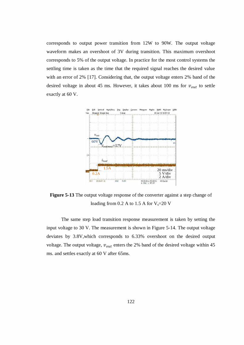
122
corresponds to output power transition from 12W to 90W. The output voltage
waveform makes an overshoot of 3V during transition. This maximum overshoot
corresponds to 5% of the output voltage. In practice for the most control systems the
settling time is taken as the time that the required signal reaches the desired value
with an error of 2% [17]. Considering that, the output voltage enters 2% band of the
desired voltage in about 45 ms. However, it takes about 100 ms for to settle
exactly at 60 V.
Figure 5-13 The output voltage response of the converter against a step change of
loading from 0.2 A to 1.5 A for Vs=20 V
The same step load transition response measurement is taken by setting the
input voltage to 30 V. The measurement is shown in Figure 5-14. The output voltage
deviates by 3.8V,which corresponds to 6.33% overshoot on the desired output
voltage. The output voltage, enters the 2% band of the desired voltage within 45
ms. and settles exactly at 60 V after 65ms.
20 ms/div5 V/div2 A/div
vout
iload
vout(max)=57V60V
0.2A
1.5A

123
Figure 5-14 The output voltage response of the converter against a step change of
loading from 0.2 A to 1.5 A for Vs=30 V
The characteristics of the step responses shown in Figure 5-13 and Figure
5-14 are similar. The reason for this similarity is that, both of the step loading
disturbances applied to the converter under 20 V and 30 V input voltages cause the
converter to change its operating mode from DCM-3 to DCM-2 operation. In this
work DCM-3 operation of the converter is not analyzed, although under no-load
condition it is inevitable that the converter operates in DCM-3 operation.
The reverse step changes of the previous two measurements are also taken.
The output load current is decreased from half to no-load instantaneously for 20 V
and 30 V input voltages. The output voltage responses of the converter against a step
change in loading for the two different input voltages are given in Figure 5-15 and
Figure 5-16.
From Figure 5-15 it is seen that the output voltage enters 2% band of the
desired voltage within 40 ms. However, it takes 90 ms for to reach its steady-
state value. Additionally the output voltage makes an overshoot of 3.8V which is
6.33% of the desired voltage.
20 ms/div5 V/div2 A/div
iload
0.2A
1.5A
vout
vout(max)=56.2V
60V
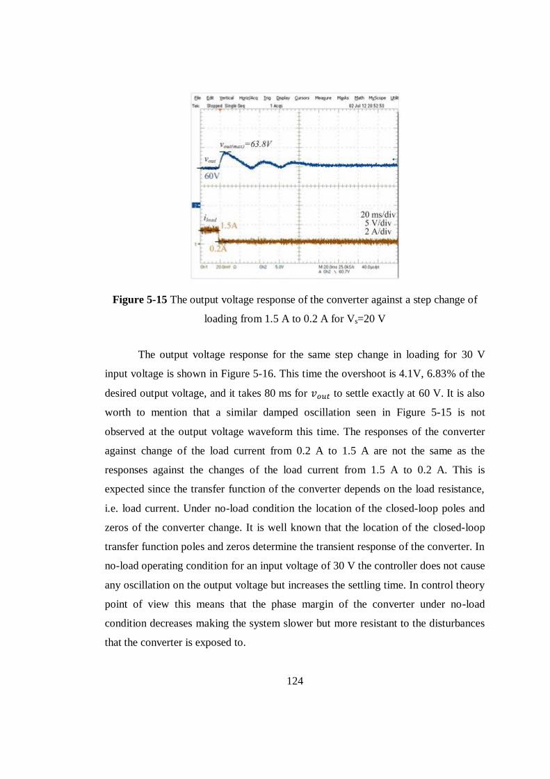
124
Figure 5-15 The output voltage response of the converter against a step change of
loading from 1.5 A to 0.2 A for Vs=20 V
The output voltage response for the same step change in loading for 30 V
input voltage is shown in Figure 5-16. This time the overshoot is 4.1V, 6.83% of the
desired output voltage, and it takes 80 ms for to settle exactly at 60 V. It is also
worth to mention that a similar damped oscillation seen in Figure 5-15 is not
observed at the output voltage waveform this time. The responses of the converter
against change of the load current from 0.2 A to 1.5 A are not the same as the
responses against the changes of the load current from 1.5 A to 0.2 A. This is
expected since the transfer function of the converter depends on the load resistance,
i.e. load current. Under no-load condition the location of the closed-loop poles and
zeros of the converter change. It is well known that the location of the closed-loop
transfer function poles and zeros determine the transient response of the converter. In
no-load operating condition for an input voltage of 30 V the controller does not cause
any oscillation on the output voltage but increases the settling time. In control theory
point of view this means that the phase margin of the converter under no-load
condition decreases making the system slower but more resistant to the disturbances
that the converter is exposed to.
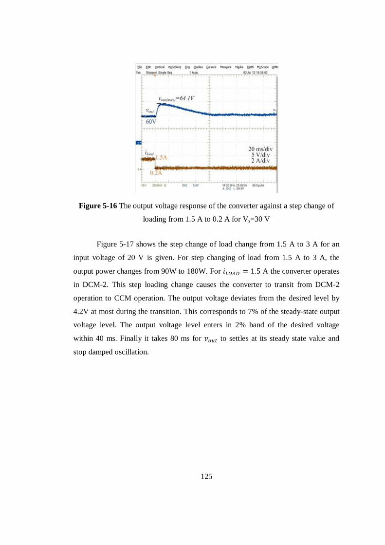
125
Figure 5-16 The output voltage response of the converter against a step change of
loading from 1.5 A to 0.2 A for Vs=30 V
Figure 5-17 shows the step change of load change from 1.5 A to 3 A for an
input voltage of 20 V is given. For step changing of load from 1.5 A to 3 A, the
output power changes from 90W to 180W. For A the converter operates
in DCM-2. This step loading change causes the converter to transit from DCM-2
operation to CCM operation. The output voltage deviates from the desired level by
4.2V at most during the transition. This corresponds to 7% of the steady-state output
voltage level. The output voltage level enters in 2% band of the desired voltage
within 40 ms. Finally it takes 80 ms for to settles at its steady state value and
stop damped oscillation.

126
Figure 5-17 The output voltage response of the converter against a step loading from
1.5 A to 3 A for Vs=20 V
A half- to full-load step loading is applied to the converter for 30 V input
voltage also. The snapshot of the measurement is given in Figure 5-18. The
overshoot in output voltage response is 2.7V, corresponding to 4.5% of the reference
voltage. It takes 25 ms for to enter into the 2% band of the desired output
voltage and 50 ms to settle at exactly 60 V.
Figure 5-18 The output voltage response of the converter against a step loading from
1.5 A to 3 A for Vs=30 V
iload
1.5A
3A
vout
60V
vout(max)=55.8V
20 ms/div5 V/div2 A/div

127
Now the reverse transition for the step loading change presented in the
previous two figures will be introduced. The output voltage variation against output
unloading change from 3 A to 1.5 A for input voltages of 20 V and 30 V are given in
Figure 5-19 and Figure 5-20 . The output power decreases from 180W to 90W during
this output voltage transition.
As shown from Figure 5-19, the overshoot voltage for 20 V input voltage
case is 3.7V (6.16% of reference voltage). The output voltage enters 2% band of the
desired voltage within 65ms. However it takes 120 ms. for to settle at exactly 60
V.
Figure 5-19 The output voltage response of the converter against a step unloading
from 3 A to 1.5 A for Vs=20 V
Figure 5-20 shows the output voltage response against the step change of the
output unloading from 3 A to 1.5 A. The output voltage deviates 2.1V at most from
the desired voltage level. This corresponds to an overshoot of 3.5%. Within 20 ms,
the output voltage enters to 2% band of the desired voltage. It takes about 40 ms for
the output voltage to settle at 60 V.

128
Figure 5-20 The output voltage response of the converter against a step unloading
from 3 A to 1.5 A for Vs=30 V
The most challenging part for the designed controller are transitions from no-
load to full-load and full-load to no-load operations. In these transitions the operating
mode of the converter changes from CCM to DCM-3. The controller performance is
tested for these step changes of loading for input voltages of 20 V and 30 V. The
output power changes from 12W to 180W and 180W to 12W during these output
voltage transitions.
The output voltage variation during the transition from no-load to full-load
condition under 20 V input voltage is shown in Figure 5-21. The output voltage
waveforms exhibits 7V overshoot (11.66% overshoot). The settling-time is 50 ms for
2% band, 80 ms for exact value of the desired output voltage value.
20 ms/div5 V/div2 A/div
iload
1.5A
3A
vout
60V
vout(max)=62.1V

129
Figure 5-21 The output voltage response of the converter against a step increase of
loading from 0.2 A to 3 A for Vs=20 V
Figure 5-22 shows the output voltage variation for the same step loading
disturbance applied at 30 V input voltage. The output voltage waveform decreases
down to 54.8V (8.66% overshoot) 5 ms after the step disturbance is applied. The
output voltage enters into the 2% band of the desired voltage within 40 ms. However,
it takes about 60 ms for to settle down at exactly 60 V.
Figure 5-22 The output voltage responses of the converter against a step increase of
loading from 0.2 A to 3 A for Vs=30 V
iload
0.2A
3A
vout
60V
vout(max)=53V
20 ms/div5 V/div2 A/div

130
Finally the reverse of the transition applied in the last two measurements are
introduced as a step disturbance to the converter. Figure 5-23 shows the output
voltage response against a step unloading from full- to no-load for an input voltage
of 20 V. deviates by 7V from the desired output voltage during this transition,
which corresponds to 11.66% overshoot. The settling time is 60 ms. for the output
voltage.
Figure 5-23 The output voltage response of the converter against a step unloading
from 3 A to 0.2 A for Vs=20 V
Figure 5-24 shows the output voltage variation during the transition of load
current from full-load to no-load for an input voltage of 30 V. The maximum value
of the output voltage is 66.5V during the transition (10.83% overshoot). The output
voltage settles down at its reference value within 100 ms.

131
Figure 5-24 The output voltage response of the converter against a step unloading
from 3 A to 0.2 A for Vs=30 V
5.3.2 Comments on the Output Voltage Responses Against Step
Output Loading Changes
The closed-loop performance of the controller against step load change is
tested in the previous part. The first thing to mention is that since the converter has
non-linear characteristic, hence responses against reverse step changes gives
different responses. For example half-load to full-load gives different response than
the one obtained for a step change from full-load to half load. This is expected since
the transfer function of the converter varies according to the operating point of the
converter. The most severe test condition is transition between full-load to no-load
operations. The maximum overshoot voltages are observed on these measurements.
The output voltage makes at most 11.66% overshoot in the whole operating range of
the converter. In general the output voltage has less overshoot and settles faster to its
reference value when the input voltage is 30 V. This is mainly due to the fact that the
controller of the converter is designed considering the full-load operation under 30 V
input voltage. It is expected that the gain and phase margins of the closed-loop
transfer function of the controller change when the input voltage and load current
20 ms/div5 V/div2 A/div
vout
60V
vout(max)=66.5V

132
change. This affects the transient response of the converter, i.e. overshoot voltage
and settling time.
5.3.3 The Output Voltage Responses Against Step Changes of the
Input Voltage
In this part the responses of the output voltage against the input voltage step
change is investigated. The source power supply is controlled by a computer,
connected to the instrument using the General Purpose Interface Bus (GPIB)
connection so that the output voltage of the power supply can be changed via a
command send to the instrument from the computer.
Before giving the measurement results, it is worth to mention about the
dynamic response of the source power supply. The power supply is capable of
increasing its output voltage in a step manner. However, for the opposite case that is
for decreasing the output voltage of the supply, the dynamic response of the power
supply is not satisfactory. Under light load conditions it takes about 80 ms for the
supply to decrease its output voltage to the required low level. Hence, it can be
concluded that, the response of the converter against a step increase in input voltage
can be examined, but the response against a step decrease in the input voltage cannot
be examined. The response of the converter against a linear decrease of the input
voltage might be called as the ramp response.
The measurements are taken again with the same oscilloscope used before.
Again a 50 V offset voltage is added to channel 2 of the oscilloscope so that the
output voltage variation is examined more precisely. This time, the measurements are
taken with a voltage division scale 2V/div since the overshoot in the output voltage
against a step change in the input voltage is lower relative to the step change in the
output loading. The measurements are taken at no-load, half-load and full-load
output loading conditions. In these each output loading conditions, the input voltage
is increased from 20 V to 30 V and decreased from 30 V to 20 V.

133
The first measurement is shown in Figure 5-25. Output loading is set to 0.2 A
and the input voltage is increased from 20 V to 30 V instantaneously. As seen from
Figure 5-25, the maximum overshoot in the output voltage is 0.8V corresponding to
1.3% of the required output voltage. It takes about 80 ms for the output voltage to
settle down exactly at 60 V. Note that the output voltage never exceeds out of 2%
band of the desired output voltage during the transition.
Figure 5-25 The output voltage response of the converter against a step change of
the input voltage from 20 V to 30 V for iLoad=0.2 A
The same step input change is applied to the converter for half-load
condition. The related measurement is given in Figure 5-26. The maximum
overshoot is 1.6V which is 2.6% of the desired output voltage. The output voltage
enters into 2% band within 20 ms. However, it takes about 60 ms to settle exactly at
60 V.
20 ms/div10 V/div(Ch1)2 V/div(Ch2)
20V
30V
vout
60V
vout(max)=60.8V

134
Figure 5-26 The output voltage response of the converter against a step change of
the input voltage from 20 V to 30 V for iLoad=1.5 A
Finally the output voltage regulation against a step increase from 20 V to 30
V in input voltage under full-load condition is shown in Figure 5-27. Note that the
maximum overshoot in this case is 3.6V. The exact settling time is 70 ms for the
output voltage. It enters into 2% band within 40 ms.
Figure 5-27 The output voltage response of the converter against a step change of
input voltage from 20 V to 30 V for iLoad=3 A
20 ms/div10 V/div(Ch1)2 V/div(Ch2)
20V
30V
vout
60V
vout(max)=61.6V
20V
30V
20 ms/div10 V/div(Ch1)2 V/div(Ch2)
vout
60V
vout(max)=63.6V

135
As mentioned before the input voltage cannot be decreased instantaneously
due to the natural characteristic of the source power supply. The large internal
capacitors at the output of the power supply are needed to be discharged fast so that
the output voltage of the power supply can be decreased. This, however, is directly
related to the current delivery capability of the source power supply. Usually the
source current of the power supply is much greater than its sink current. That is why
the supply can increase its output voltage instantaneously but cannot decrease it at an
equal rate. Hence the output voltage response against linearly decaying input voltage
can be considered as ramp input response of the converter. The responses of the
output voltage against such linear decay of input voltage are given in this work to
gain an insight about designed converter.
The first measurement is taken under no-load condition and shown in Figure
5-28. The output voltage never exceeds 2% band. Actually it deviates only by 0.2V
at maximum during the transition which corresponds to 0.33% of the output voltage.
In this case it is meaningless to mention about the settling time since the deviation is
very low. Note that the input power supply output voltage decreases to 20 V within
80 ms.
Figure 5-28 The output voltage response of the converter against a ramp input
voltage decay from 30 V to 20 V for iLoad=0.2 A

136
The second measurement for the input voltage level decay from 30 V to 20 V
is taken for operation with half-load. The response is shown in Figure 5-29. The
output voltage deviates by 1.4V which corresponds to 2.3% of the output voltage.
The output voltage settles at 60 V in about 80 ms.
Figure 5-29 The output voltage response of the converter against a ramp input
voltage decay from 30 V to 20 V for iLoad=1.5 A
The last measurement for the input voltage linear decay from 30 V to 20 V is
taken under full-load operation. The maximum overshoot on this response is 2.4V
which is 4% of the output voltage. It takes about 110 ms for the output voltage to
settle exactly at 60 V. However for the 2% band of the output voltage settling time is
about 80 ms.
20 ms/div10 V/div(Ch1)2 V/div(Ch2)
20V
30V
vout
60Vvout(max)=58.6V

137
Figure 5-30 The output voltage response of the converter against a ramp input
voltage decay from 30 V to 20 V for iLoad=3 A
5.4 The Efficiency Analysis of the Prototype Converter from
Experimental Results
In this part the efficiency of the prototype converter will be determined. The
efficiency analysis is one of the most important aspects of the converter design. All
the power losses on the components involved with the prototype converter will be
determined analytically so that the total power loss of the converter can be found.
The switches (MOSFETs), input and rectification diodes, inductors,
capacitors and the isolation transformer cause power losses in the Z-source
converter. For proper determination of the power loss, the current passing through
these components must be identified. The notations and directions of the current
passing through these components are shown in Figure 5-31.
20 ms/div10 V/div(Ch1)2 V/div(Ch2)
20V
30V
vout
60V
vout(max)=57.6V
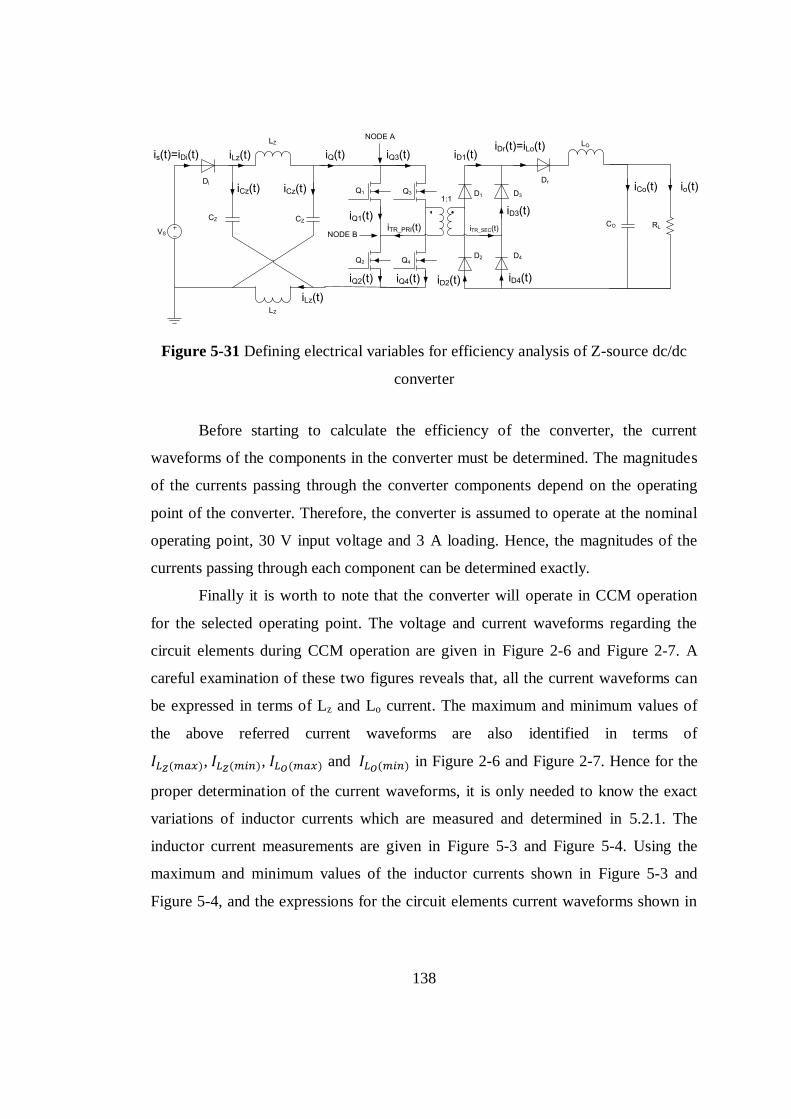
138
Figure 5-31 Defining electrical variables for efficiency analysis of Z-source dc/dc
converter
Before starting to calculate the efficiency of the converter, the current
waveforms of the components in the converter must be determined. The magnitudes
of the currents passing through the converter components depend on the operating
point of the converter. Therefore, the converter is assumed to operate at the nominal
operating point, 30 V input voltage and 3 A loading. Hence, the magnitudes of the
currents passing through each component can be determined exactly.
Finally it is worth to note that the converter will operate in CCM operation
for the selected operating point. The voltage and current waveforms regarding the
circuit elements during CCM operation are given in Figure 2-6 and Figure 2-7. A
careful examination of these two figures reveals that, all the current waveforms can
be expressed in terms of Lz and Lo current. The maximum and minimum values of
the above referred current waveforms are also identified in terms of
, , and in Figure 2-6 and Figure 2-7. Hence for the
proper determination of the current waveforms, it is only needed to know the exact
variations of inductor currents which are measured and determined in 5.2.1. The
inductor current measurements are given in Figure 5-3 and Figure 5-4. Using the
maximum and minimum values of the inductor currents shown in Figure 5-3 and
Figure 5-4, and the expressions for the circuit elements current waveforms shown in
VS
Di
CZ CZ
LZ
LZ
LO
CO RL
Dr
is(t)=iDi(t)
iCz(t) iCz(t)
iLz(t) iQ(t)iDr(t)=iLo(t)
iCo(t) io(t)
iLz(t)
Q3
Q4
1:1D1
D2
Q1
Q2
D3
D4
iQ1(t)
iQ2(t)
iQ3(t)
iQ4(t)
iD1(t)
iD3(t)
iD2(t) iD4(t)
iTR_PRI(t) iTR_SEC(t)
NODE A
NODE B

139
Figure 2-6 and Figure 2-7 it is possible to obtain the current waveforms regarding the
circuit elements of the converter which are shown in Figure 5-32 and Figure 5-33.
Figure 5-32 Determination of current waveform magnitudes regarding the circuit
elements for open-loop control
t
t
t
t
t
t
Duty-Factor
t1=3.38us t2=6.62us t1=3.38us t2=6.62us
TS=10us TS=10us
İLo(t)
İCo(t)
İTR_PRI(t)
İTR_SEC(t)
İD1(t)
İD4(t)
İD2(t)
İD3(t)
ILo(max)=5.3A
ILo(min)=0.68A
ILo(max)=5.3A
ILo(min)=0.68A
ICo(max)=2.31A
ICo(min)=-2.31A
ICo(max)=2.31A
ICo(min)=-2.31
ITR(2)=0.68A
ITR(3)=5.3A
ITR(1)=-0.68A
ITR(0)=-5.3A
ITR(2)=0.68A
ITR(1)=-0.68A
ITR(0)=-5.3A
IDr(min)=0.68A
IDr(max)=5.3A
IDr(min)=0.68A
IDr(max)=5.3A
IDr(min)=0.68A
IDr(max)=5.3A
IDr(min)=0.68A
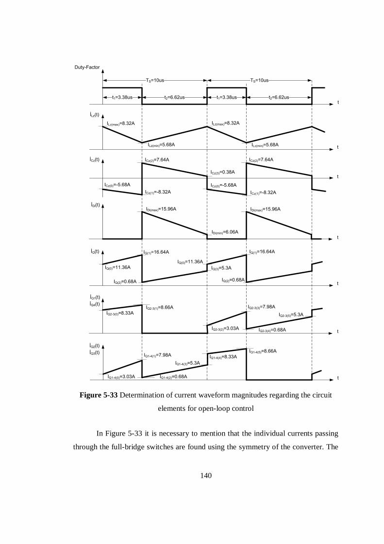
140
Figure 5-33 Determination of current waveform magnitudes regarding the circuit
elements for open-loop control
In Figure 5-33 it is necessary to mention that the individual currents passing
through the full-bridge switches are found using the symmetry of the converter. The
t
t
t
t
t
t
Duty-Factor
t1=3.38us t2=6.62us t1=3.38us t2=6.62us
TS=10us TS=10us
İLz(t)
İCz(t)
İDi(t)
İQ1(t)
İQ4(t)
İQ2(t)
İQ3(t)
ILz(max)=8.32A
ILz(min)=5.68A
ILz(max)=8.32A
ILz(min)=5.68A
ICz(0)=-5.68A
ICz(1)=-8.32A
IQ1-4(2)=0.68A
IQ1-4(3)=5.3A
IQ1-4(5)=8.66A
ICz(2)=7.64A
ICz(3)=0.38A
ICz(0)=-5.68A
ICz(1)=-8.32A
ICz(2)=7.64A
IDi(max)=15.96A
IDi(min)=6.06A
IDi(max)=15.96A
t
İQ(t)
IQ(2)=0.68A
IQ(3)=5.3AIQ(0)=11.36A
IQ(1)=16.64A
IQ(0)=11.36A
IQ(1)=16.64A
IQ(2)=0.68A
IQ1-4(0)=3.03A
IQ1-4(1)=7.98A IQ1-4(4)=8.33A
IQ2-3(1)=8.66A
IQ2-3(0)=8.33A
IQ2-3(2)=3.03A
IQ2-3(3)=7.98A
IQ2-3(4)=0.68A
IQ2-3(5)=5.3A

141
instantaneous is equal to
and is equal to
due to the
symmetry of the converter. This property will be used to determine the exact values
of the current passing through the switches.
Applying Kirchhoff’s current law at ‘NODE A’ yields;
(5.1)
Similarly one can conclude that;
(5.2)
One obtains (5.3) by the application of Kirchhoff’s current law at ‘NODE B’
(5.3)
In a similar way it is also possible to obtain (5.4).
(5.4)
Combining (5.1)-(5.4) the sum of and
is found as;
(5.5)
Since, as mentioned before regarding that
, one obtains;
(5.6)
Using (5.6) each switch current can be determined. The values are shown in
Figure 5-33.
5.4.1 Power Loss Calculation on the Switches (MOSFETs) from the
Experimental Results
The switch power losses are due to two processes. The first one is the on-state
losses. It is also known as the conduction losses, and is due to the on-state

142
voltage drop of the switch during the conduction of current. The second one is the
switching losses, . It is due to the variation of the voltage and current
related to the switch during turn-on and turn-off periods.
In [1] it is mentioned that, the switching loss of a MOSFET can be
approximated as;
(5.7)
The turn on time, ton is the time for the switch to transit from blocking state to
conduction stat and can be found analytically as [20];
The turn off time, toff is the time for the switch to transit from conduction
state to blocking state and can be found analytically as [20];
The definitions of the parameters used in the formulas of ton and toff are given
in Table 5-2.

143
Table 5-2 Definitions of the parameters used in ton and toff formula
Parameter Definition
MOSFET drain-source voltage
MOSFET drain-source current
MOSFET gate-source voltage when
it is ON
MOSFET gate driving resistance
MOSFET threshold voltage
MOSFET transconductance
MOSFET input capacitance
MOSFET reverse transfer
capacitance
In the drive circuit of the MOSFET, is 13.5V due to the darlington
output structure of the driver IC. is set as 15Ω in the driver circuit. In the
converter design, IPB065N15N3+G from INFINEON is used for the full-bridge
MOSFETs. The threshold voltage, of the MOSFET is stated as 3V typically in
its datasheet [24]. The transconductance, is typically 139S. Also from the
datasheet it is known that mosfet input capacitance, is 5.5nF (typically) and
reverse capacitance, is 10pF (typically) for IPB065N15N3+G. The MOSFET
drain-source voltage, is 90 V during the transition from ‘on’ state to ‘off’ state
and from ‘off’ state to ‘on’ state. The current passing through the MOSFET during
turn-on is 3.03 A and 8.66 A during turn-off as seen from Figure 5-33. At this step it
is necessary to clarify one point. The reverse capacitance of a MOSFET changes
dramatically during the plateau region, in which falls. Hence it is usually
preferred to define the reverse capacitance, as (5.8) in order to determine the
turn on time.

144
(5.8)
where , and stand for the gate-drain capacitance, gate-
drain charge and voltage swing seen on the drain-source connection of the MOSFET.
(5.8) must be substituted into ton and toff formula in order to determine turn on and
turn off times properly. is found as 11 nC (typical) from the datasheet. The
voltage swing is 90 V during the operation.
Finally inserting the numerical data into the formulas given for ton and toff,
one obtains the turn-on time as ton=15.92ns and toff=55.57ns. Note that, the effective
switching frequency is 50 kHz for each MOSFET throughout the operation. Hence
switching loss of one MOSFET is;
𝑊
The conduction loss of a MOSFET is defined as;
(5.9)
The on state resistance of the MOSFET is given as 5.2 mΩ (typical) in the
datasheet. The RMS current of the MOSFET can be found analytically using the
current waveform of the MOSFET shown in Figure 5-33. The magnitude of RMS
current passing through the MOSFET is found to be 4.605 A. Hence the conduction
loss in one MOSFET is;
𝑊
Now, the total loss on MOSFET can be found by adding up the switching and
conduction loss.
(5.10)
𝑊 𝑊 𝑊

145
5.4.2 Power Loss Calculation of the Switches (Diodes) from the
Experimental Results
The power losses in diodes are due to the switching and conduction as in the
case of MOSFETs. However, in the prototype converter fast schotky diodes are used
which are known to have no switching loss or very little switching loss that can be
neglected. Hence the diodes have only the conduction loss which is due to the on
state voltage drop of the diodes. The conduction loss of a diode can be calculated as;
(5.11)
The input diode of the converter is selected as 40CTQ150SPbf from
International Rectifier [25]. The forward voltage drop on the diode is 0.71V. The
average current passing through it can be calculated from the current waveform
given in Figure 5-33 as;
(5.12)
Hence the power dissipation on the input diode is;
𝑊 (5.13)
For the rectification diodes, V60120C is used which is again a product of
VISHAY. The forward voltage drop of V60120C is found from the datasheet of the
product as 0.55V [26]. The average current of the rectification diode can be found
from the related current waveform given in Figure 5-32 as;
(5.14)
Hence the power dissipation on the rectification diode is;

146
𝑊 (5.15)
5.4.3 Power Loss Calculation of the Capacitors from the
Experimental Results
The power loss of the capacitor is due to its equivalent series resistance
(ESR) and the ac current passing through it. The power dissipation of a capacitor can
be expressed as;
(5.16)
Note that, the RMS value of the ac current passing through the capacitor must
be taken into consideration in order to determine the power dissipation. In Z-source
dc/dc converter both Z-source network impedance capacitor, and the output filter
capacitor, cause power dissipation. Hence the RMS of both Z-source capacitor
current, and filter capacitor current
must be determined.
For Z-source network capacitor, C1210X105K1RAC (1uF, 100 V ceramic
capacitor), product of AVX, is used [27]. Here twenty many capacitors are connected
in parallel to obtain 20 µF. Recalling that the ceramic capacitors are known to have
the lowest ESR among the capacitor families. Paralleling twenty of them will give a
very low ESR and in return will reduce the total power dissipation. The ESR of one
capacitor is stated as 100mΩ at 100 kHz in the datasheet. Hence paralleling twenty
of them will reduce the ESR to 5mΩ. The RMS of Z-source capacitor current, can
be determined analytically from Figure 5-33 as 5.511 A. Hence the power dissipation
on is;
𝑊 (5.17)
For the output filter capacitor of the converter, A710160 (aluminum
electrolytic type capacitor) from SICSAFCO Company is used [28]. The ESR of
A710160 is 51mΩ at 100 Hz. It is mentioned in the catalog that the ESR at 100 kHz

147
is typically 1.5xESR100Hz. Hence the ESR of the output capacitor can be accepted as
76.5 mΩ The RMS of the output filter capacitor current, is found to be 1.33 A
from Figure 5-33. Hence the power dissipation on is;
𝑊 (5.18)
5.4.4 Power Loss Calculation of the Inductors from the
Experimental Results
The inductor losses are composed of two components. The first is the core
loss which occurs in the inductor core. The second one is the copper loss due to the
windings around the coil former of the inductor core. The copper loss is mainly due
to the average inductor current passing through the inductor. However, the ripple of
the inductor current causes power dissipation also on the ac resistance of the
windings, which is due to the proximity effect [16].
ETD59/31/22 N87 B6639762000X1 cores from EPCOS are used for the Z-
source network inductors. Two AWG16 copper wires are paralleled and 16 turns of
this wire is wounded around the coil former of the core so that 83.3 µ inductance is
obtained. The copper wires are paralleled in order to decrease the dc resistance of the
winding.
The core loss of an inductor is related to the B-H characteristics of the core
material. The flux density B(t) is expressed as the summation of a dc component B
(due to the dc value of magnetizing current) and ac component ∆B (due to the ac
current ripple). The maximum value of B(t) throughout the operation must be lower
than the saturation flux density of the core Bsat. for inductor core is found
as;
(5.19)

148
where , , o and
represent, the number of turns wounded
around core, maximum instantaneous current passing through the Z-source
network inductor, permeability of vacuum and the air gap of core,
respectively [16]. For Lz inductor core air gap is 2mm and the maximum current
passing through it is 8.32 A. The total number of turns, is determined as 16
before and the permeability of the vacuum s known o be π -7. Hence,
inserting the numerical data in (5.19), one obtains =0.0856T. The
saturation flux density of the selected core for Lz is 0.390T. Thus the core will
not saturate throughout the operation.
The amplitude of determines the core loss of inductor.
is found
as;
(5.20)
where is the voltage across the inductor during D.Ts and
is the
effective area in the magnetic cross-section of the core [16]. Recalling (2.3), (2.16)
and (2.18), the voltage across the Z-source inductor, is 60 V during D.Ts. The
effective magnetic cross section of the core is found to be 368 mm2 from the
datasheet [29].
Finally, referring to Figure 5-33, it is obvious that D=0.338 and Ts=10 s.
Thus,
(5.21)
To determine the core loss, “Core Loss vs. AC Field Flux Density Curve”
graph provided by the manufacturer must be used [30]. Using the provided
information in [30], it is found out that the core loss/volume of , is 4kW/m3.

149
The volume of the core, is found to be 51200 mm
3 from datasheet. Hence the
total core loss of , is;
(5.22)
𝑊 𝑊
The windings of the inductor are wound with AWG16 copper wire whose
resistance is 0.0132Ω/m. The effective turn length of the coil former is
106.1mm and 16 turns are wounded. Recalling that two copper wires are paralleled
for the winding, so that dc resistance of the inductor is;
(5.23)
From the dowell’s curve the ratio of ac resistance to dc resistance is found as
13, yielding that [19]. The copper loss of the inductor can be
found as;
(5.24)
where
(5.25)
Using the resistance and current values determined, total copper loss of the Z-
source network inductor is;
𝑊 (5.26)
Hence the total power loss of the Z-source inductor is;
𝑊 (5.27)

150
The same procedure will be applied for the power loss calculation of the
output filter inductor, Lo. ETD54/28/19 N87 B66395G2000X1 core, whose air gap
is 2mm, from EPCOS is used for the output filter inductor [31]. Two AWG16
copper wires are paralleled and 19 turns of wire ( ) is wounded around the
coil former to have an inductance of 50 µH. Referring to Figure 5-32, the maximum
output filter current, is 5.3 A. Applying (5.19) for core, the maximum
flux density, is 0.063T during the operation. The saturation flux density of
core is 0.390T, so that the core will not saturate throughout the operation. The
amplitude of is;
(5.28)
The voltage across the output filter inductor, is -60 V. Since we are
interested in the magnitude of , one can take
as 60 V. The effective
magnetic cross section of core, is found as 280 mm
2 from datasheet [31].
Inserting these numerical value into (5.20) and recalling that D=0.338 and Ts=10 s
for the operation one obtains as;
(5.29)
Referring to the “Core Loss vs. AC Field Flux Density Curve” graph
provided by the manufacturer, the core loss/volume of Lo, is 5kW/m3. The
volume of the core, is found to be 35600 mm
3 from datasheet. Hence the total
core loss of , is;
(5.30)
𝑊 𝑊

151
The windings of the inductor are wound with AWG16 copper wire whose
resistance is 0.0132Ω/m. The effective turn length of the coil former, is 96mm
and 19 turns are wounded [31]. Recalling that two copper wires are paralleled for the
winding, so that dc resistance of the inductor is;
(5.31)
From the dowell’s curve the ratio of ac resistance to dc resistance is found as
13, yielding that [19]. The copper loss of the inductor can be
found as;
(5.32)
where
(5.33)
Using the resistance and current values determined, total copper loss of the
output inductor is;
𝑊 (5.34)
Hence the total power loss of the output inductor is;
𝑊 (5.35)
5.4.5 Power Loss Calculation of the Isolation Transformer from the
Experimenatl Results
The transformer loss is composed of the core loss and the copper loss. For the
isolation transformer OR45530 R from Magnetics Company is used [32]. The

152
primary side and the secondary side of the isolation transformer have 11 turns of
AWG12 wire.
The amplitude of ac flux density change, must be determined in order
to calculate the core loss of the transformer. The amplitude of is given as;
(5.36)
In (5.36), λ represents the volt-seconds applied to the transformer during the
positive portion of the transformer input voltage waveform. Transformer input
voltage waveform is 90 V for a time duration of 6.62µs. Hence the volt-seconds
applied to the transformer is;
In (5.36), stands for primary number of turns, which is 11 and is the
effective magnetic cross sectional are of the transformer core, which is found to be
420mm2 from the “Magnetics Ferrite Cores Catalog”. Hence the amplitude of
is;
(5.37)
The core loss of the transformer can be determined from the “Core Loss vs.
Flux Density” curve given in Magnetics Ferrite Materials Specification Catalog. The
core loss/ volume of the transformer core, is found as 15mw/cm3
[33]. The
volume of the transformer core, is given as 52cm3 in the datasheet. Hence the
core loss of the transformer is calculated as;
(5.38)
𝑊 𝑊
It is now necessary to calculate the copper loss of the transformer. The
effective turn length of the coil former used for the transformer core, is

153
11.38cm. The resistance of an AWG12 wire is 0.00521Ω/m. Hence the dc resistance
of the transformer primary and secondary side is;
(5.39)
From the Dowell’s curve the ratio of ac resistance to dc resistance is found as
7, yielding that [19]. The copper loss of the transformer is only
due to its ac resistance since the average current passing through the transformer over
one switching period is zero. Hence, considering that primary and secondary sides
have equal number of turns, the copper loss of the transformer can be determined as;
(5.40)
Referring to Figure 5-32, the RMS current of the transformer is calculated as
3.28 A, yielding;
𝑊 (5.41)
Hence the total power loss of the isolation transformer is;
𝑊 (5.42)
5.4.6 Comparison of the Measured and Calculated Efficiency of the
Prototype Converter
The power dissipation of each element in Z-source dc/dc converter is
calculated in the previous part. Hence the efficiency of the converter can be
determined by summing up the calculated power dissipations of each element. Note
that the Z-source capacitor and inductor dissipations must be multiplied by 2.
Moreover the switch (MOSFET) and rectification diodes power dissipations are
needed to be multiplied by four due to the converter topology. Hence the total power
dissipation of the converter is;

154
(5.43)
𝑊
For the determination of the measured efficiency, the output voltage and
current of the input power supply of Z-source dc/dc converter is recorded. Note that
the used power supply is calibrated regularly. Under the operating condition, at
which the efficiency analysis is conducted, the output voltage and current of the
supply is 30 V and 6.80 A. The output voltage of the Z-source dc/dc converter is set
to 60 V under full-load, 3 A. Hence the measured efficiency of Z-source dc/dc
converter is;
(5.44)
𝑊
There is slight difference between the measured and calculated power
dissipation. This might be due to ringing phenomena observed on the rectifier diodes.
Ringing phenomena observed during the switching instants might cause addition
power dissipation which is not taken into consideration in the analytical calculation
of efficiency. Moreover, the resistances of the wires wound around the inductor and
transformer cores increase as the temperature of the wires increase. This causes
additional copper loss power dissipation on inductors and transformer. Finally the
theoretical calculation of turn-on and turn-off time does not give the exact value of
the measured turn-on and turn-off times. The theoretical calculation does not take the
package leakage inductance of the MOSFET which slows down the turn-on and turn-
off transitions. Slower turn-on and turn-off transitions will cause larger switching
losses which in turn decrease the efficiency of the converter.

155
CHAPTER 6
CONCLUSION AND FUTURE WORKS
6.1 Conclusion
In this work, the design and implementation of a Z-source full-bridge dc/dc
converter is focused. Although the full-bridge structure is buck derived topology, it is
possible to boost the input voltage using Z-source network impedance between the
source power supply and full-bridge part.
The CCM operation of Z-source dc/dc converter has been analyzed before.
However the DCM-2 operation of the converter was not dealt with before this thesis.
The input-output voltage relationships, the voltage and current waveforms of each
element in the converter structure in DCM-2 operations are provided in Chapter 2
within the scope of this work. The mathematical analysis of the component
waveforms are verified by the simulation results. Furthermore, a prototype circuit is
implemented so as to make a comparison of the theoretical analysis with the practical
results. The inductor, capacitor and switch current and voltage waveforms obtained
by the prototype converter closely match with the simulation results. However there
is slight difference for the rectifier diode voltage and current waveforms. Throughout
the analysis and simulation the components are assumed to be ideal. However, the
capacitor effective in reverse recovery of the rectifier diode and the leakage
inductance of the isolation transformer cause ringing in the rectifier diode voltage
waveform. Despite the ringing phenomena, output voltage and current waveforms

156
obtained during the implementation are satisfactory. Also, some voltage spikes are
observed in voltage waveforms of the switching elements. It is known that the stray
inductances in the prototype converter can cause such voltage spikes. However
spikes do not pose threat for the voltage breakdown of the elements.
For the controller design aspect of the converter, the dynamic model of the
converter is derived for both CCM and DCM-2 operations. The necessary transfer
functions, such as duty factor-to-output voltage and input voltage-to-output
voltage , are derived for both CCM and DCM-2 operations. The derived
transfer functions are verified with the simulation results. In the design process it is
realized that the controller design of the Z-source dc/dc converter is more
challenging relative to other well known converter topologies. The transfer function
of Z-source dc/dc converter contains four poles since it has four energy storing
elements in its structure. In addition the converter’s transfer function contains a right
half plane zero, which causes unexpected responses and slows down the dynamic
response of the converter. In many converter topologies the transfer functions of the
converters have two poles which make it easier to design a controller.
Current mode control is implemented for the prototype converter, such
control has not been considered before and hence reported so far. The output voltage
response does not involve continuous oscillations, but during the transitional period,
it exhibits damped oscillations for a limited time against a step disturbance in input
voltage or output loading. During the experiments conducted on the prototype it is
observed that such damped oscillations in the output voltage exists and lasts at most
100 ms and later the output voltage settles at exactly the desired voltage. The damped
oscillation can be suppressed to some extent by changing the pole-zero locations of
the controller. However, this will worsen the dynamic response of the converter,
settling time and overshoot. Since, no specs are imposed on the dynamic response of
the converter, it is preferred to keep the settling time and overshoot as low as
possible with a trade of a low level damped oscillatory response.

157
6.2 Future Works
In the mathematical analysis, all components in Z-source converter are
assumed to be ideal. The parasitic components, such as capacitor ESRs, diode on
state voltage drops, on state resistances of MOSFETs, leakage inductance of the
transformer and resistance of the inductors can be added to the mathematical analysis
so as to obtain a more realistic model of the converter.
In this work, the input diode current is assumed to be non-zero at all times.
However in DCM-3 operation the input diode current falls to zero. DCM-3 operation
can be analyzed in future research. For this case, it will be really difficult to follow
an analytical approach, since there will be more than three different states of the
converter. Hence, a numerical or time domain simulation based approach can be
adopted to obtain the transfer function of the converter in DCM-3 operation. Detailed
information about these approaches can be found in the literature [21]-[23].
The input diode among the other elements in the converter causes the highest
power dissipation. MOSFET can be used instead of input diode so as to increase the
efficiency of the converter. Furthermore, a Z-source resonant dc/dc converter
topology can be implemented for future research. Thus, the efficiency of the
converter can be increased and the energy storing components of the converter can
be decreased in physical sizes.
Finally, gain scheduling approach can be implemented for the control
purposes of Z-source converter. Since Z-source converter’s transfer function has 4
poles making it harder to design a controller exhibiting the same performance at
every operating point, a family of PI controllers can be designed and implemented
each of which provides satisfactory control for different operating points.
158
REFERENCES
[1]: Ned Mohan, “Power Electronics: Converters, Applications, and Design”, 3rd
edition, Publisher: Wiley 2002-10-10 ISBN 0471226939
[2]: Fuat Onur Bağlan, “Design Of an Eductional Purpose Multifunctional DC/DC
Converter Board”, Master of Science Thesis Submitted to METU, November
2008
[3]: P. Kim, S. Choi and J. Kim, “An Inductorless Asymmetrical ZVS Full Bridge
Converter for Step-up Application wit Wide Input Voltage Range”, IEE Energy
Conversion, Congress and Exposition, ECCE, pp. 1945, Atlanta USA, 12-16
Sept. 2010
[4]: K.B.Park, C.E.Kim,G.W.Moon, and M.J.Yoon, “Voltage Oscillation Reduction
Techniques for Phase-Shift Full-Bridge Converter,” IEEE Transactions on
Industrial Electronics, Oct. 2007
[5]: Guan-Chyun Hsieh and Tuzng-Hang Yang, “Step-Up ZVS Full-Bridge
Converter with Loss Reduction by Forward Energy-Delivered Circuit”, Vehicle
Power and Propulsion Conference, VPPC '08. IEEE, 3-5 Sept. 2008
[6]: Lizhi Zhu, “A Novel Soft-Commutating Isolated Boost Full-Bridge ZVS-PWM
DC–DC Converter for Bidirectional High Power Applications,” IEEE
Transactions, Power Electronics, March 2006

159
[7]: Fang Zheng Peng, Honnyong Cha, Dong-Wook Yoo, “Distributed Impedance
Network (Z-Network) DC-DC Converter” IEEE Transactions on Power
Electronics, Vol. 25, No. 11, November 2010
[8]: Fang Zheng Peng, “Z-Source Inverter,” IEEE Transaction on Industry
Applications, Vol.39, No.2, April 2003
[9]: Fang Zheng Peng, “Z-Source Networks for Power Conversion” Applied Power
Electronics Conference and Exposition, Feb. 2008
[10]: Xu-Peng Fang, “Three-Phase Z-Source AC-AC Converter for Motor Drives”,
Power Electronics and Motion Control Conference, 2006. IPEMC 2006.
CES/IEEE 5th International, Aug. 2006
[11]: Honnyon Cha, Fang Z.Peng and Dongwook Yoo, “Z-source Resonant DC-DC
Converter for Wide Input Voltage and Load Variation”, International Power
Electronics Conference, 2010
[12]: Xupeng Fang, Xingquan Ji, “Bidirectional Power Flow Z-Source DC-DC
Converter”, IEEE Vehicle and Propulsion Conference (VPPC), Sep. 2008
[13]: Ji Zhang, Jing Ge, “Analysis Z-Source DC-DC Converter in Discontinuous
Current Mode”, 2010
[14]: Çağdaş Pekuz, “Z-Source, Full Bridge DC/DC Converter”, Master of Science
Thesis Submitted to METU, December 2010
[15]: Indrek Roasto, Dmitri Vinnikov, “Analysis and Evaluation of PWM and PSM
Shoot-Through Control Methods for Voltage-Fed qZSI Based DC/DC

160
Converters”, 14th International Power Electronics and Motion Control
Conference, EPE-PEMC 2010
[16]: Robert Warren Erickson, Dragan Maksimovic Springer, “The Fundamentals of
Power Electronics”, 2001 ISBN 0-7923-7270-0
[17]: Katsuhiko Ogata, “Modern Control Engineering”, 4th
Edition 2002
[18]: Mustafa Tufan Ayhan, “Design and Implementation of Coupled Inductor Cuk
Converter Operating in Continuous Conduction Mode”, Master of Science
Thesis Submitted to METU, December 2011
[19]: P.L. Dowell, “Effects of Eddy Currents in Transformer Windings,” Proceeding
IEE (UK), Vol.113, No.8, August 1966
[20]: Jess Brown, “Power MOSFET Basics: Understanding Gate Charge and Using it
to Assess Switching Performance” VISHAY AN608, December 2004
[21]: D. Maksimovic, “Automated Small-Signal Analysis of Switching Converters
Using a General-Purpose Time-Domain Simulator”, Applied Power Electronics
Conference, Feb. 1998
[22]: A. Davoudi, “Numerical state-space average-value modeling of PWM DC-DC
converters operating in DCM and CCM”, IEEE Transaction on Power
Electronics, July 2006
[23]: C. Fernandez, “Frequency Response of Switching DC/DC Converters From a
Single Simulation in the Time Domain”, Applied Power Electronics Conference
and Exposition, March 2011
Manufacturer Data

161
[24]: “IPB065N15N3 G Datasheet”, INFINEON, 2010
[25]: “40CTQ150 Datasheet”, INTERNATIONAL RECTIFIERS, 2007
[26]: “V60120C Datasheet”, VISHAY, 2009
[27]: “C1210X105K1RACTU Datasheet”, KEMET, 2006
[28]: “SICSAFCO Catalog pp. 76-77”, SICSAFCO, 2009
[29]: “ETD59/31/22 Datasheet”, EPCOS, 2006
[30]: “SIFERRIT MATERIAL N87 Datasheet”, EPCOS, 2006
[31]: “ETD54/28/19 Datasheet”, EPCOS, 2006
[32]: “MAGNETICS Short Form Catalog pp. 19-20”, MAGNETICS, 2009
[33]: “MAGNETICS Materials-Section-3 pp. 1-5”, MAGNETICS, 2009
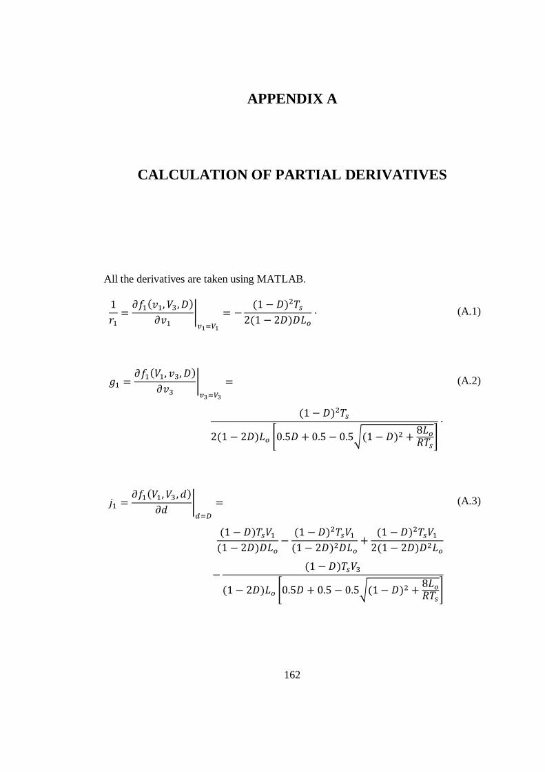
162
APPENDIX A
CALCULATION OF PARTIAL DERIVATIVES
All the derivatives are taken using MATLAB.
(A.1)
(A.2)
(A.3)

163
(A.4)
(A.5)
(A.6)

164
(A.7)
(A.8)

165

166
APPENDIX B
PROTOTYPE CONVERTER CIRCUIT SCHEMATICS
Figure B-1 Sheet 1 of the prototype converter circuit schematics

167
Figure B-2 Sheet 2 of the prototype converter circuit schematics

168
Figure B-3 Sheet 3 of the prototype converter circuit schematics
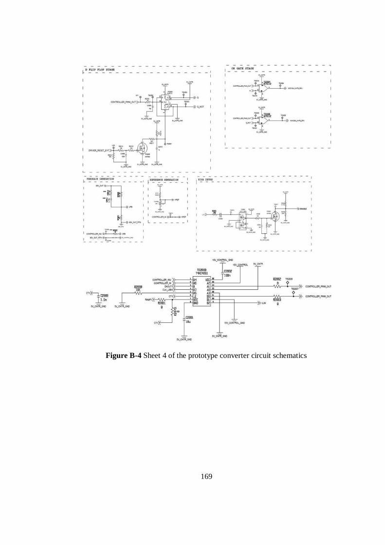
169
Figure B-4 Sheet 4 of the prototype converter circuit schematics

170
APPENDIX C
PROTOTYPE CONVERTER CIRCUIT LAYOUT
Figure C-1 Top side layout of the prototype converter
Figure C-2 Bottom side layout of the prototype converter